Embed Size (px)
Citation preview
Features _äìÉ`çêÉ∆=_`SNPM»=nck Next generation, high-quality, low-cost, mono
headset solution with extremely low-cost eBOM World's longest talk time: up to 18 hours time from
a small 120mAh battery Proximity Pairing (heaset initiated pairing) Advanced Multipoint Programmable Audio Prompts Built-in echo and noise reduction Integrated CSR AuriStream ® low-power codec Support for Secure Simple Pairing Best-in-class Bluetooth radio with 7.5dBm
transmit power and -92dBm receive sensitivity Pin compatible with BlueVox2 QFN Configurable mono headset software HFP v1.5 and HSP v1.1 support Integrated 1.5V and 1.9V linear regulators Integrated switch-mode regulator Integrated 150mA lithium battery charger Integrated high-quality mono codec 48-lead 7 x 7 x 0.9mm, 0.5mm pitch QFN Green (RoHS compliant and no antimony or
halogenated flame retardants) Complete BC6130 low-cost mono headset
solution development kit, includes exampledesign, order code DK-BC-6130-1A
BC6130 Low-cost Mono HeadsetSolution
Fully Qualified Single-chipBluetooth® v2.1 + EDR system
Production Information
BC6130A04
Issue 2
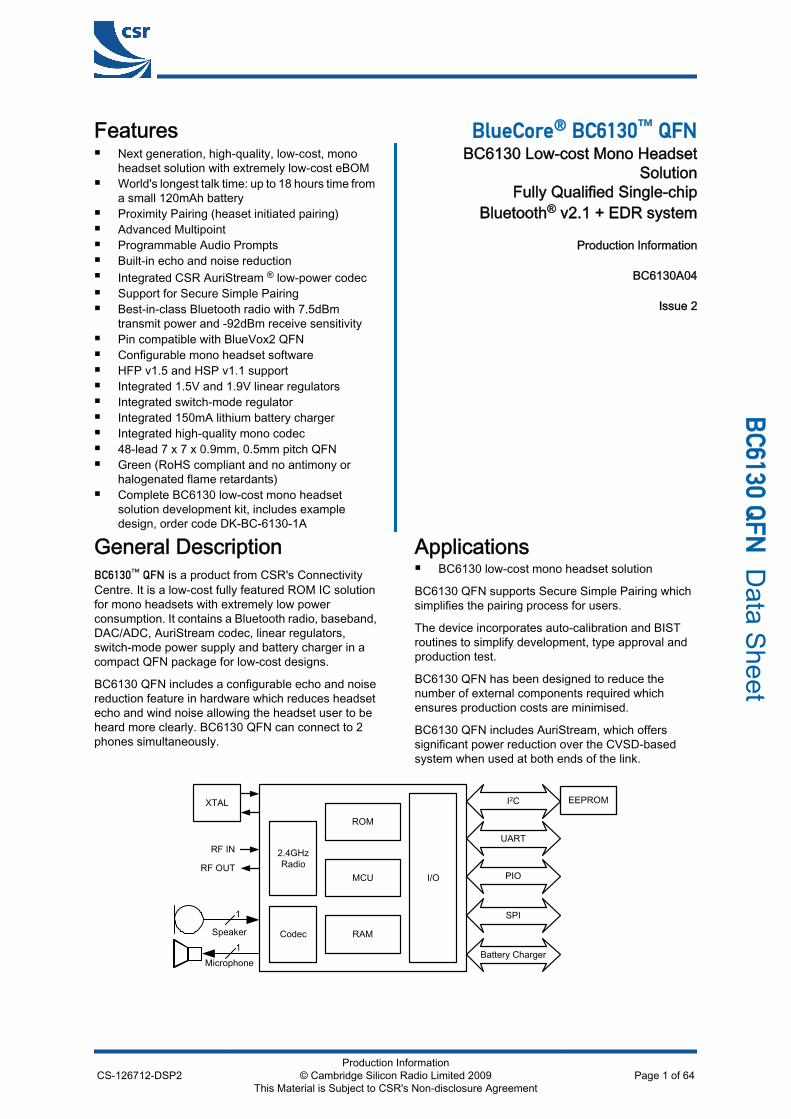
General Description_`SNPM»=nck is a product from CSR's ConnectivityCentre. It is a low-cost fully featured ROM IC solutionfor mono headsets with extremely low powerconsumption. It contains a Bluetooth radio, baseband,DAC/ADC, AuriStream codec, linear regulators,switch-mode power supply and battery charger in acompact QFN package for low-cost designs.
BC6130 QFN includes a configurable echo and noisereduction feature in hardware which reduces headsetecho and wind noise allowing the headset user to beheard more clearly. BC6130 QFN can connect to 2phones simultaneously.
Applications BC6130 low-cost mono headset solution
BC6130 QFN supports Secure Simple Pairing whichsimplifies the pairing process for users.
The device incorporates auto-calibration and BISTroutines to simplify development, type approval andproduction test.
BC6130 QFN has been designed to reduce thenumber of external components required whichensures production costs are minimised.
BC6130 QFN includes AuriStream, which offerssignificant power reduction over the CVSD-basedsystem when used at both ends of the link.
I/O
2.4GHz Radio
XTAL
Microphone
Speaker
RF IN
RF OUT
Codec
1
1
SPI
Battery Charger
PIO
UART
I2C EEPROM
MCU
RAM
ROM
CS-126712-DSP2Production Information
© Cambridge Silicon Radio Limited 2009This Material is Subject to CSR's Non-disclosure Agreement
Page 1 of 64
_`SNPM=n
ck Data Sheet
Document HistoryRevision Date Change Reason1 10 JUN 09 Original publication of this document.2 08 JUL 09 Production Information.
Power consumption figures confirmed.Tape and Reel information updated for clarityIf you have any comments about this document, email [email protected] givingthe number, title and section with your feedback.
Document History
CS-126712-DSP2Production Information
© Cambridge Silicon Radio Limited 2009This Material is Subject to CSR's Non-disclosure Agreement
Page 2 of 64
_`SNPM=n
ck Data Sheet
Status InformationThe status of this Data Sheet is Production Information.
CSR Product Data Sheets progress according to the following format:
Advance Information
Information for designers concerning CSR product in development. All values specified are the target values of thedesign. Minimum and maximum values specified are only given as guidance to the final specification limits and mustnot be considered as the final values.
All detailed specifications including pinouts and electrical specifications may be changed by CSR without notice.
Pre-production Information
Pinout and mechanical dimension specifications finalised. All values specified are the target values of the design.Minimum and maximum values specified are only given as guidance to the final specification limits and must not beconsidered as the final values.
All electrical specifications may be changed by CSR without notice.
Production Information
Final Data Sheet including the guaranteed minimum and maximum limits for the electrical specifications.
Production Data Sheets supersede all previous document versions.
Life Support Policy and Use in Safety-critical Applications
CSR's products are not authorised for use in life-support or safety-critical applications. Use in such applications isdone at the sole discretion of the customer. CSR will not warrant the use of its devices in such applications.
CSR Green Semiconductor Products and RoHS Compliance
BC6130 QFN devices meet the requirements of Directive 2002/95/EC of the European Parliament and of the Councilon the Restriction of Hazardous Substance (RoHS).
BC6130 QFN devices are also free from halogenated or antimony trioxide-based flame retardants and otherhazardous chemicals. For more information, see CSR's Environmental Compliance Statement for CSR GreenSemiconductor Products.
Trademarks, Patents and Licences
Unless otherwise stated, words and logos marked with ™ or ® are trademarks registered or owned by CSR plc or itsaffiliates. Bluetooth® and the Bluetooth logos are trademarks owned by Bluetooth SIG, Inc. and licensed to CSR.Other products, services and names used in this document may have been trademarked by their respective owners.
The publication of this information does not imply that any license is granted under any patent or other rights ownedby CSR plc and/or its affiliates.
CSR reserves the right to make technical changes to its products as part of its development programme.
While every care has been taken to ensure the accuracy of the contents of this document, CSR cannot acceptresponsibility for any errors.
Refer to www.csrsupport.com for compliance and conformance to standards information.
Status Information
CS-126712-DSP2Production Information
© Cambridge Silicon Radio Limited 2009This Material is Subject to CSR's Non-disclosure Agreement
Page 3 of 64
_`SNPM=n
ck Data Sheet
Contents1 Device Details ................................................................................................................................................. 82 Functional Block Diagram .............................................................................................................................. 93 Package Information ..................................................................................................................................... 10
3.1 Pinout Diagram .................................................................................................................................... 103.2 Device Terminal Functions .................................................................................................................. 113.3 Package Dimensions ........................................................................................................................... 143.4 PCB Design and Assembly Considerations ......................................................................................... 153.5 Typical Solder Reflow Profile ............................................................................................................... 15
4 Bluetooth Modem .......................................................................................................................................... 164.1 RF Ports ............................................................................................................................................... 16
4.1.1 RF_N and RF_P ..................................................................................................................... 164.2 RF Receiver ......................................................................................................................................... 16
4.2.1 Low Noise Amplifier ............................................................................................................... 164.2.2 RSSI Analogue to Digital Converter ....................................................................................... 16
4.3 RF Transmitter ..................................................................................................................................... 174.3.1 IQ Modulator .......................................................................................................................... 174.3.2 Power Amplifier ...................................................................................................................... 17
4.4 Bluetooth Radio Synthesiser ............................................................................................................... 174.5 Baseband ............................................................................................................................................. 17
4.5.1 Burst Mode Controller ............................................................................................................ 174.5.2 Physical Layer Hardware Engine ........................................................................................... 17
4.6 AuriStream Codec ............................................................................................................................... 174.7 Basic Rate Modem .............................................................................................................................. 184.8 Enhanced Data Rate Modem .............................................................................................................. 18
5 Clock Generation .......................................................................................................................................... 195.1 Clock Architecture ................................................................................................................................ 195.2 Input Frequencies and PS Key Settings .............................................................................................. 195.3 Crystal Oscillator: XTAL_IN and XTAL_OUT ....................................................................................... 19
5.3.1 Load Capacitance .................................................................................................................. 215.3.2 Frequency Trim ...................................................................................................................... 215.3.3 Transconductance Driver Model ............................................................................................ 225.3.4 Negative Resistance Model ................................................................................................... 225.3.5 Crystal PS Key Settings ......................................................................................................... 22
5.4 External 32kHz Clock .......................................................................................................................... 226 Bluetooth Stack Microcontroller .................................................................................................................... 24
6.1 Programmable I/O (PIO) Parallel Ports ............................................................................................... 247 Memory Interface and Management ............................................................................................................. 25
7.1 Memory Management Unit .................................................................................................................. 257.2 System RAM ........................................................................................................................................ 257.3 Internal ROM ....................................................................................................................................... 25
8 Serial Interfaces ............................................................................................................................................ 268.1 UART Interface .................................................................................................................................... 26
8.1.1 UART Configuration While Reset is Active ............................................................................ 278.2 Programming and Debug Interface ...................................................................................................... 27
8.2.1 Instruction Cycle ..................................................................................................................... 288.2.2 Multi-slave Operation ............................................................................................................. 28
8.3 I2C Interface ......................................................................................................................................... 289 Audio Interface .............................................................................................................................................. 29
9.1 Audio Input and Output ........................................................................................................................ 299.2 Mono Audio Codec Block Diagram ...................................................................................................... 29
Contents
CS-126712-DSP2Production Information
© Cambridge Silicon Radio Limited 2009This Material is Subject to CSR's Non-disclosure Agreement
Page 4 of 64
_`SNPM=n
ck Data Sheet
9.2.1 ADC ........................................................................................................................................ 299.2.2 ADC Digital Gain .................................................................................................................... 299.2.3 ADC Analogue Gain ............................................................................................................... 309.2.4 DAC ........................................................................................................................................ 309.2.5 DAC Digital Gain .................................................................................................................... 319.2.6 DAC Analogue Gain ............................................................................................................... 319.2.7 Microphone Input ................................................................................................................... 319.2.8 Line Input ............................................................................................................................... 349.2.9 Output Stage .......................................................................................................................... 359.2.10 Integrated Digital Filter ........................................................................................................... 369.2.11 Side Tone ............................................................................................................................... 37
10 Power Control and Regulation ...................................................................................................................... 3810.1 Power Sequencing ............................................................................................................................... 3810.2 External Voltage Source ...................................................................................................................... 3810.3 Switch-mode Regulator ....................................................................................................................... 3910.4 High-voltage Linear Regulator ............................................................................................................. 3910.5 Low-voltage Linear Regulator .............................................................................................................. 3910.6 Voltage Regulator Enable Pins ............................................................................................................ 3910.7 Battery Charger ................................................................................................................................... 4010.8 LED Drivers ......................................................................................................................................... 4010.9 Reset, RST# ........................................................................................................................................ 41
10.9.1 Digital Pin States on Reset .................................................................................................... 4210.9.2 Status after Reset .................................................................................................................. 42
11 Example Application Schematic ................................................................................................................... 4312 Electrical Characteristics .............................................................................................................................. 44
12.1 ESD Precautions ................................................................................................................................. 4412.2 Absolute Maximum Ratings ................................................................................................................. 4412.3 Recommended Operating Conditions .................................................................................................. 4412.4 Input/Output Terminal Characteristics ................................................................................................. 45
12.4.1 High-voltage Linear Regulator ............................................................................................... 4512.4.2 Switch-mode Regulator .......................................................................................................... 4612.4.3 Low-voltage Linear Regulator ................................................................................................ 4712.4.4 Battery Charger ...................................................................................................................... 4812.4.5 Reset ...................................................................................................................................... 4912.4.6 Regulator Enable ................................................................................................................... 4912.4.7 Digital Terminals .................................................................................................................... 5012.4.8 LED Driver Pads .................................................................................................................... 5112.4.9 Auxiliary ADC ......................................................................................................................... 5112.4.10 Mono Codec: Analogue to Digital Converter .......................................................................... 5212.4.11 Mono Codec: Digital to Analogue Converter .......................................................................... 5312.4.12 Clocks .................................................................................................................................... 53
13 Power Consumption ..................................................................................................................................... 5414 CSR Green Semiconductor Products and RoHS Compliance ..................................................................... 55
14.1 RoHS Statement .................................................................................................................................. 5514.1.1 List of Restricted Materials ..................................................................................................... 55
15 CSR Bluetooth Software Stack ..................................................................................................................... 5615.1 BC6130 Low-cost Mono Headset Solution Development Kit ............................................................... 5615.2 BC6130 Low-cost Mono Headset Solution Software (BC6130A04) .................................................... 5615.3 Advanced Multipoint Support ............................................................................................................... 5615.4 Programmable Audio Prompts ............................................................................................................. 5715.5 Proximity Pairing .................................................................................................................................. 57
15.5.1 Proximity Pairing Configuration .............................................................................................. 5716 Ordering Information ..................................................................................................................................... 58
16.1 BC6130 Low-cost Mono Headset Solution Development Kit Ordering Information ............................ 58
Contents
CS-126712-DSP2Production Information
© Cambridge Silicon Radio Limited 2009This Material is Subject to CSR's Non-disclosure Agreement
Page 5 of 64
_`SNPM=n
ck Data Sheet
17 Tape and Reel Information ........................................................................................................................... 5917.1 Tape Orientation .................................................................................................................................. 5917.2 Tape Dimensions ................................................................................................................................. 6017.3 Reel Information .................................................................................................................................. 6117.4 Moisture Sensitivity Level .................................................................................................................... 61
18 Document References .................................................................................................................................. 62Terms and Definitions ............................................................................................................................................ 63
List of FiguresFigure 2.1 Functional Block Diagram ................................................................................................................. 9Figure 3.1 Device Pinout .................................................................................................................................. 10Figure 4.1 Simplified Circuit RF_N and RF_P .................................................................................................. 16Figure 4.2 BDR and EDR Packet Structure ..................................................................................................... 18Figure 5.1 Clock Architecture ........................................................................................................................... 19Figure 5.2 Crystal Driver Circuit ....................................................................................................................... 20Figure 5.3 Crystal Equivalent Circuit ................................................................................................................ 20Figure 8.1 Break Signal .................................................................................................................................... 26Figure 8.2 Example EEPROM Connection ...................................................................................................... 28Figure 9.1 Mono Codec Audio Input and Output Stages .................................................................................. 29Figure 9.2 ADC Analogue Amplifier Block Diagram ......................................................................................... 30Figure 9.3 Microphone Biasing ......................................................................................................................... 32Figure 9.4 Differential Input .............................................................................................................................. 35Figure 9.5 Single-ended Input .......................................................................................................................... 35Figure 9.6 Speaker Output ............................................................................................................................... 35Figure 10.1 Voltage Regulator Configuration ..................................................................................................... 38Figure 10.2 LED Equivalent Circuit .................................................................................................................... 41Figure 11.1 Example Application Schematic ...................................................................................................... 43Figure 15.1 Programmable Audio Prompts in External I2C EEPROM ............................................................... 57Figure 17.1 Tape Orientation ............................................................................................................................. 59Figure 17.2 Tape Dimensions ............................................................................................................................ 60Figure 17.3 Reel Dimensions ............................................................................................................................. 61
List of TablesTable 4.1 Data Rate Schemes ......................................................................................................................... 18Table 5.1 Crystal Specification ......................................................................................................................... 20Table 8.1 Possible UART Settings ................................................................................................................... 26Table 8.2 Standard Baud Rates ....................................................................................................................... 27Table 8.3 Instruction Cycle for a SPI Transaction ............................................................................................ 28Table 9.1 ADC Digital Gain Rate Selection ...................................................................................................... 30Table 9.2 DAC Digital Gain Rate Selection ...................................................................................................... 31Table 9.3 DAC Analogue Gain Rate Selection ................................................................................................. 31Table 9.4 Voltage Output Steps ....................................................................................................................... 33Table 9.5 Current Output Steps ....................................................................................................................... 34Table 10.1 BC6130 QFN Voltage Regulator Enable Pins .................................................................................. 40Table 10.2 Pin States on Reset .......................................................................................................................... 42
List of EquationsEquation 5.1 Load Capacitance ........................................................................................................................... 21Equation 5.2 Trim Capacitance ............................................................................................................................ 21Equation 5.3 Frequency Trim ............................................................................................................................... 21
Contents
CS-126712-DSP2Production Information
© Cambridge Silicon Radio Limited 2009This Material is Subject to CSR's Non-disclosure Agreement
Page 6 of 64
_`SNPM=n
ck Data Sheet
Equation 5.4 Pullability ......................................................................................................................................... 21Equation 5.5 Transconductance Required for Oscillation .................................................................................... 22Equation 5.6 Equivalent Negative Resistance ..................................................................................................... 22Equation 8.1 Baud Rate ....................................................................................................................................... 26Equation 9.1 IIR Filter Transfer Function, H(z) ..................................................................................................... 37Equation 9.2 IIR Filter plus DC Blocking Transfer Function, HDC(z) .................................................................... 37Equation 10.1LED Current .................................................................................................................................... 41Equation 10.2LED PAD Voltage ............................................................................................................................ 41
Contents
CS-126712-DSP2Production Information
© Cambridge Silicon Radio Limited 2009This Material is Subject to CSR's Non-disclosure Agreement
Page 7 of 64
_`SNPM=n
ck Data Sheet
1 Device Details
Radio Common TX/RX terminal simplifies external
matching; eliminates external antenna switch BIST minimises production test time Bluetooth v2.1 + EDR specification compliant
Transmitter 7.5dBm RF transmit power with level control from
on-chip 6-bit DAC over a dynamic range >30dB Class 2 and Class 3 support without the need for an
external power amplifier or TX/RX switch
Receiver Receiver sensitivity of -92dBm Integrated channel filters Digital demodulator for improved sensitivity and co-
channel rejection Real-time digitised RSSI available on HCI interface Fast AGC for enhanced dynamic range
Synthesiser Fully integrated synthesiser requires no external
VCO, varactor diode, resonator or loop filter Compatible with crystals 16MHz to 26MHz
Baseband and Software Internal ROM 48KB internal RAM, allows full-speed data transfer,
mixed voice and data, and full piconet operation,including all EDR packet types
Logic for forward error correction, header errorcontrol, access code correlation, CRC,demodulation, encryption bit stream generation,whitening and transmit pulse shaping; supports allmandatory Bluetooth v2.1 + EDR specificationfeatures including eSCO and AFH
Transcoders for A-law, µ-law and linear voice fromhost and A-law, µ-law and CVSD voice over air
AuriStream codec, offers significant powerreduction over the CVSD-based system when usedat both ends of the link
Configurable mono headset ROM software to set-up headset features and UI
Support for HFP v1.5, including three-way calling,and HSP v1.1
Support for Bluetooth v2.1 + EDR specificationSecure Simple Pairing
Proximity Pairing (heaset initiated pairing) Advanced Multipoint support, allowing the headset
to connect to 2 phones or 1 phone and a VoIPdongle
Built-in echo and noise reduction hardware
Auxiliary Features Crystal oscillator with built-in digital trimming Device can run in low power modes from an external
32.768kHz clock signal Power management includes digital shutdown, and
wake up commands with an integrated low-poweroscillator for ultra-low power Park/Sniff/Hold mode
On-chip regulators: 1.5V output from 1.7V to 2.8Vinput and 1.9V output from 2.7V to 5.5V input
On-chip high-efficiency switched-mode regulator;1.5V output from 2.2V to 4.4V input
Power-on-reset cell detects low supply voltage Arbitrary sequencing of power supplies allowed 10-bit ADC Battery charger with programmable current, 20 to
150mA, for lithium ion/polymer battery 2 LED drivers with faders
Audio Codec 16-bit resolution mono codec Integrated amplifiers for driving 16Ω speakers; no
need for external components Support for single-ended speaker termination and
line output Integrated low-noise microphone bias Digital enhancements to add bass cut and side tone Analogue enhancements to support single-ended
speaker drive capability and reference availability
Physical Interfaces Synchronous serial interface for system debugging I²C compatible interface used to communicate with
an external EEPROM which contains all of thedevice configuration (PS Keys)
UART interface with data rates up to 3Mbits/s
Mono Headset Software Complete on-chip part to operate as a Bluetooth
mono headset, including all the protocol layers: HCI RFCOMM Bluetooth profiles
Package Option 48-lead 7 x 7 x 0.9mm, 0.5mm pitch QFN described
in this document
Device Details
CS-126712-DSP2Production Information
© Cambridge Silicon Radio Limited 2009This Material is Subject to CSR's Non-disclosure Agreement
Page 8 of 64
_`SNPM=n
ck Data Sheet
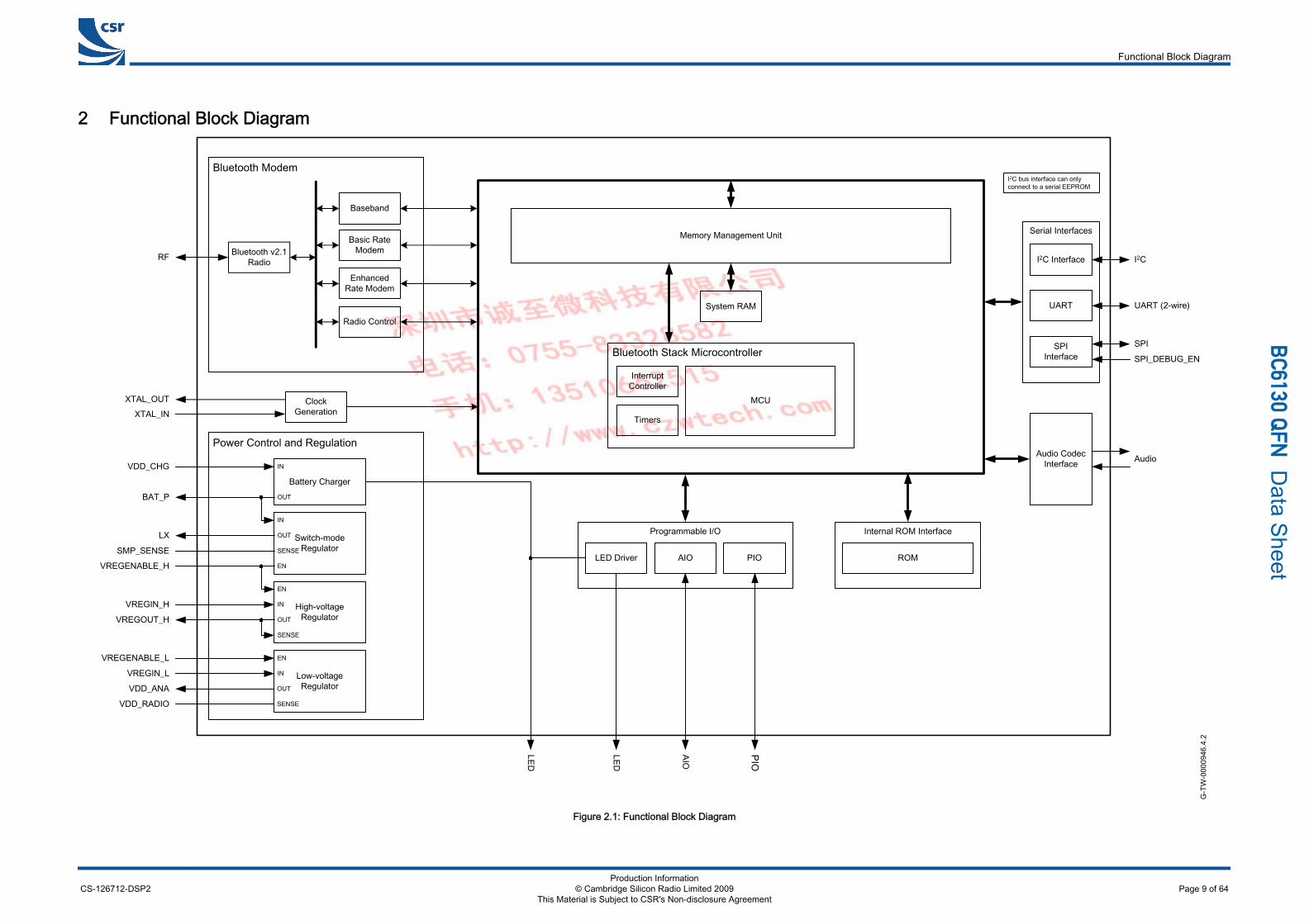
2 Functional Block Diagram
G-T
W-0
0009
46.4
.2
Power Control and Regulation
VDD_CHG
LED
I2C bus interface can only connect to a serial EEPROM
Memory Management Unit
System RAM
Audio Codec Interface Audio
Internal ROM Interface
ROM
Programmable I/O
LED Driver AIO PIO
LED
AIO
PIO
BAT_P
VREGENABLE_H
LX
SMP_SENSE
VREGIN_H
VREGOUT_H
VREGENABLE_L
VREGIN_L
VDD_ANA
VDD_RADIO
Bluetooth Stack Microcontroller
MCU
InterruptController
Timers
Serial Interfaces
UART
I2C Interface I2C
SPIInterface
SPI
RF
Switch-mode Regulator
High-voltage Regulator
Low-voltage Regulator
Battery Charger
IN
OUT
EN
IN
OUT
EN
SENSE
OUT
IN
EN
IN
OUT
SENSE
SENSE
UART (2-wire)
XTAL_OUTXTAL_IN
Bluetooth Modem
Basic Rate Modem
Enhanced Rate Modem
Radio Control
Baseband
Bluetooth v2.1 Radio
Clock Generation
SPI_DEBUG_EN
Figure 2.1: Functional Block Diagram
Functional Block Diagram
CS-126712-DSP2Production Information
© Cambridge Silicon Radio Limited 2009This Material is Subject to CSR's Non-disclosure Agreement
Page 9 of 64
_`SNPM=n
ck Data Sheet
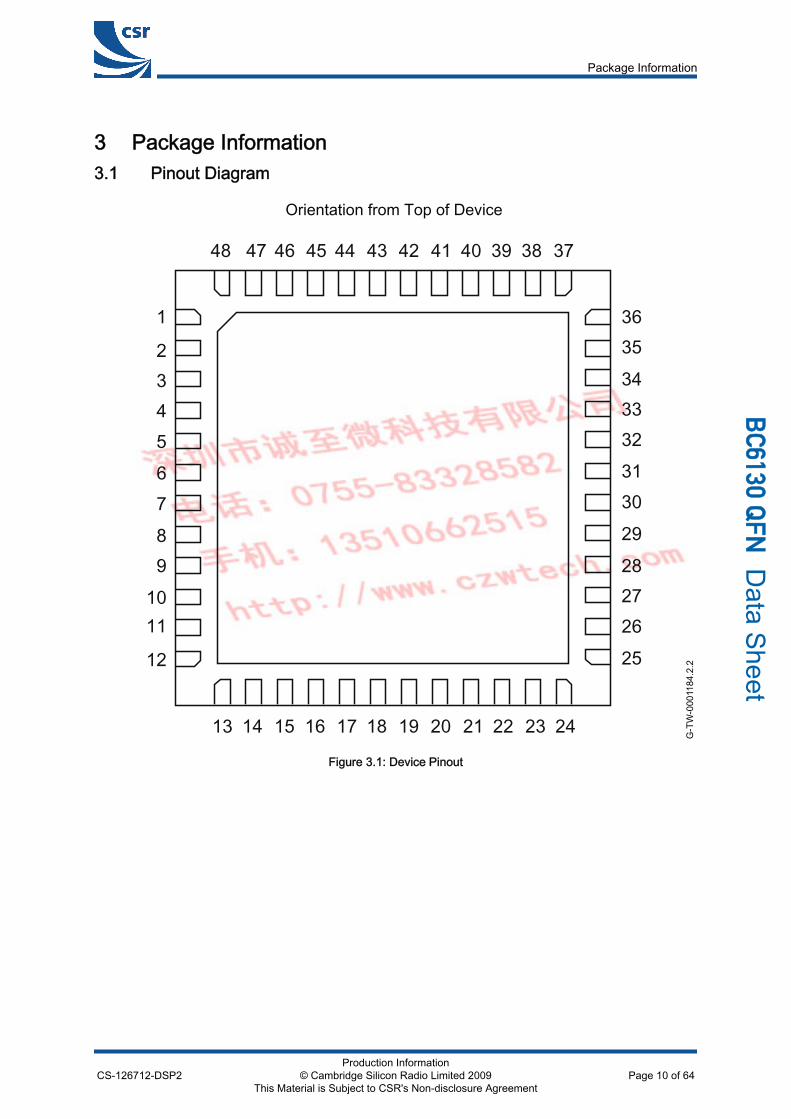
3 Package Information3.1 Pinout Diagram
G-T
W-0
0011
84.2
.225
13
1
37
23456789
1011
12
14 15 16 17 18 19 20 21 22 23 24
2627282930313233343536
3839404142434445464748
Orientation from Top of Device
Figure 3.1: Device Pinout
Package Information
CS-126712-DSP2Production Information
© Cambridge Silicon Radio Limited 2009This Material is Subject to CSR's Non-disclosure Agreement
Page 10 of 64
_`SNPM=n
ck Data Sheet
3.2 Device Terminal Functions
Bluetooth Radio Lead Pad Type Supply Domain Description
RF_N 8 RF VDD_RADIO Transmitter output/switchedreceiver
RF_P 7 RF VDD_RADIO Complement of RF_N
Synthesiser andOscillator Lead Pad Type Supply Domain Description
XTAL_IN 13 Analogue VDD_ANA For crystal or external clock input
XTAL_OUT 14 Analogue VDD_ANA Drive for crystal
LO_REF 15 Analogue VDD_ANA Reference voltage to decouple thesynthesiser
UART Interface Lead Pad Type Supply Domain Description
UART_TX 19 Bidirectional withweak internal pull-up VDD_PADS[0] UART data output, active high
UART_RX 18Bidirectional withweak internal pull-down
VDD_PADS[0] UART data input, active high
SPI Interface Lead Pad Type Supply Domain Description
SPI_MOSI 38 Input, with weakinternal pull-down VDD_PADS[1] SPI data input
SPI_CS# 40Bidirectional withweak internal pull-down
VDD_PADS[1] Chip select for SPI, active low
SPI_CLK 39Bidirectional withweak internal pull-down
VDD_PADS[1] SPI clock
SPI_MISO 41Bidirectional withweak internal pull-down
VDD_PADS[1] SPI data output
SPI_DEBUG_EN 42 Input with stronginternal pull-down VDD_PADS[1]
Enable for debug interface, activehigh. Must be enabled beforeSPI_CS#.
Package Information
CS-126712-DSP2Production Information
© Cambridge Silicon Radio Limited 2009This Material is Subject to CSR's Non-disclosure Agreement
Page 11 of 64
_`SNPM=n
ck Data Sheet
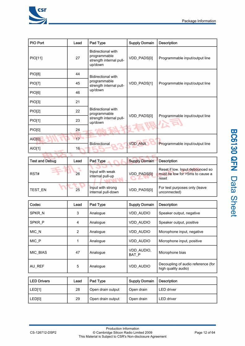
PIO Port Lead Pad Type Supply Domain Description
PIO[11] 27
Bidirectional withprogrammablestrength internal pull-up/down
VDD_PADS[0] Programmable input/output line
PIO[8] 44Bidirectional withprogrammablestrength internal pull-up/down
VDD_PADS[1] Programmable input/output linePIO[7] 45
PIO[6] 46
PIO[3] 21
Bidirectional withprogrammablestrength internal pull-up/down
VDD_PADS[0] Programmable input/output linePIO[2] 22
PIO[1] 23
PIO[0] 24
AIO[0] 17Bidirectional VDD_ANA Programmable input/output line
AIO[1] 16
Test and Debug Lead Pad Type Supply Domain Description
RST# 26 Input with weakinternal pull-up VDD_PADS[0]
Reset if low. Input debounced somust be low for >5ms to cause areset
TEST_EN 25 Input with stronginternal pull-down VDD_PADS[0] For test purposes only (leave
unconnected)
Codec Lead Pad Type Supply Domain Description
SPKR_N 3 Analogue VDD_AUDIO Speaker output, negative
SPKR_P 4 Analogue VDD_AUDIO Speaker output, positive
MIC_N 2 Analogue VDD_AUDIO Microphone input, negative
MIC_P 1 Analogue VDD_AUDIO Microphone input, positive
MIC_BIAS 47 Analogue VDD_AUDIO,BAT_P Microphone bias
AU_REF 5 Analogue VDD_AUDIO Decoupling of audio reference (forhigh quality audio)
LED Drivers Lead Pad Type Supply Domain Description
LED[1] 28 Open drain output Open drain LED driver
LED[0] 29 Open drain output Open drain LED driver
Package Information
CS-126712-DSP2Production Information
© Cambridge Silicon Radio Limited 2009This Material is Subject to CSR's Non-disclosure Agreement
Page 12 of 64
_`SNPM=n
ck Data Sheet
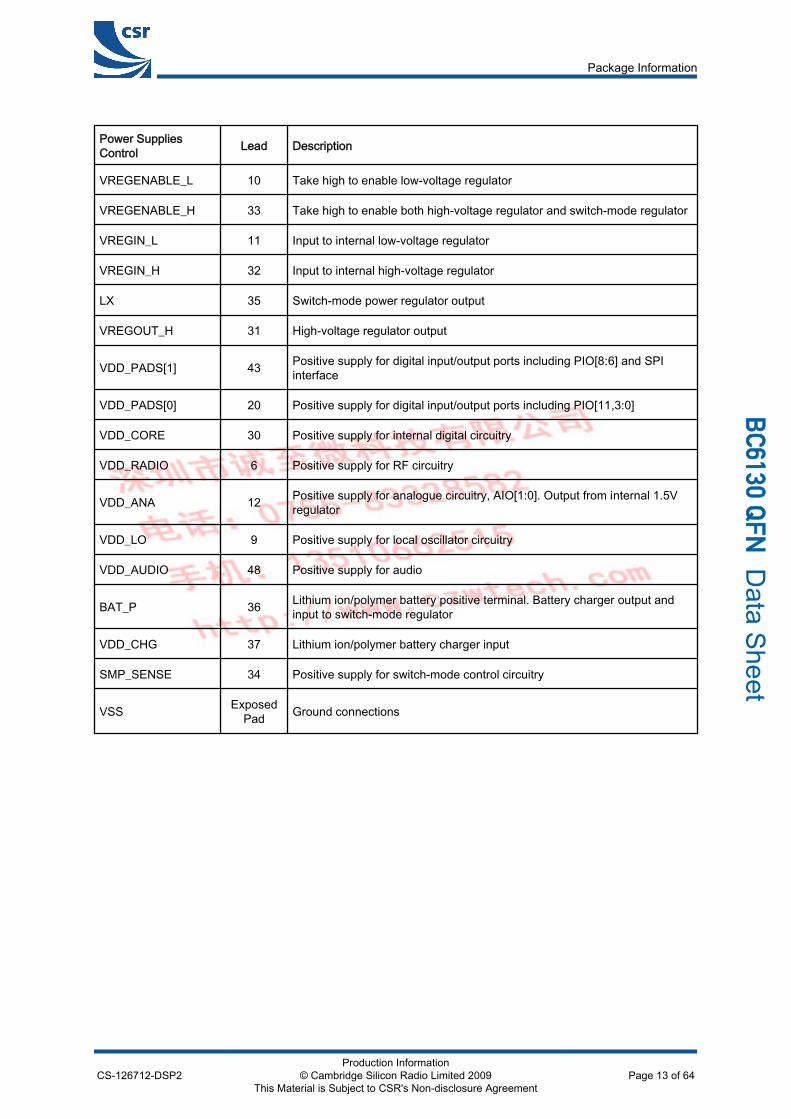
Power SuppliesControl Lead Description
VREGENABLE_L 10 Take high to enable low-voltage regulator
VREGENABLE_H 33 Take high to enable both high-voltage regulator and switch-mode regulator
VREGIN_L 11 Input to internal low-voltage regulator
VREGIN_H 32 Input to internal high-voltage regulator
LX 35 Switch-mode power regulator output
VREGOUT_H 31 High-voltage regulator output
VDD_PADS[1] 43 Positive supply for digital input/output ports including PIO[8:6] and SPIinterface
VDD_PADS[0] 20 Positive supply for digital input/output ports including PIO[11,3:0]
VDD_CORE 30 Positive supply for internal digital circuitry
VDD_RADIO 6 Positive supply for RF circuitry
VDD_ANA 12 Positive supply for analogue circuitry, AIO[1:0]. Output from internal 1.5Vregulator
VDD_LO 9 Positive supply for local oscillator circuitry
VDD_AUDIO 48 Positive supply for audio
BAT_P 36 Lithium ion/polymer battery positive terminal. Battery charger output andinput to switch-mode regulator
VDD_CHG 37 Lithium ion/polymer battery charger input
SMP_SENSE 34 Positive supply for switch-mode control circuitry
VSS ExposedPad Ground connections
Package Information
CS-126712-DSP2Production Information
© Cambridge Silicon Radio Limited 2009This Material is Subject to CSR's Non-disclosure Agreement
Page 13 of 64
_`SNPM=n
ck Data Sheet
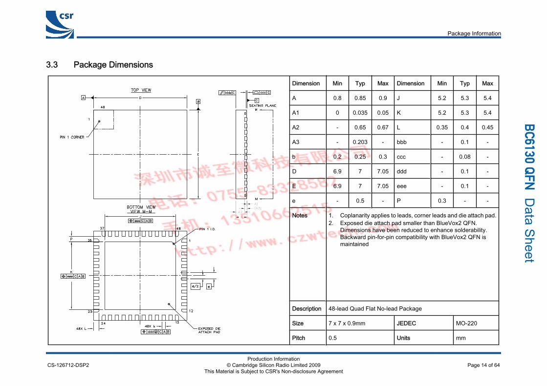
3.3 Package Dimensions
Dimension Min Typ Max Dimension Min Typ Max
A 0.8 0.85 0.9 J 5.2 5.3 5.4
A1 0 0.035 0.05 K 5.2 5.3 5.4
A2 - 0.65 0.67 L 0.35 0.4 0.45
A3 - 0.203 - bbb - 0.1 -
b 0.2 0.25 0.3 ccc - 0.08 -
D 6.9 7 7.05 ddd - 0.1 -
E 6.9 7 7.05 eee - 0.1 -
e - 0.5 - P 0.3 - -
Notes 1. Coplanarity applies to leads, corner leads and die attach pad.2. Exposed die attach pad smaller than BlueVox2 QFN.
Dimensions have been reduced to enhance solderability.Backward pin-for-pin compatibility with BlueVox2 QFN ismaintained
Description 48-lead Quad Flat No-lead Package
Size 7 x 7 x 0.9mm JEDEC MO-220
Pitch 0.5 Units mm
Package Information
CS-126712-DSP2Production Information
© Cambridge Silicon Radio Limited 2009This Material is Subject to CSR's Non-disclosure Agreement
Page 14 of 64
_`SNPM=n
ck Data Sheet
3.4 PCB Design and Assembly ConsiderationsThis section lists recommendations to achieve maximum board-level reliability of the 7 x 7 x 0.9mm QFN 48-leadpackage:
NSMD lands (lands smaller than the solder mask aperture) are preferred, because of the greater accuracyof the metal definition process compared to the solder mask process. With solder mask defined pads, theoverlap of the solder mask on the land creates a step in the solder at the land interface, which can causestress concentration and act as a point for crack initiation.
CSR recommends that the PCB land pattern to be in accordance with IPC standard IPC-7351. Solder paste must be used during the assembly process.
3.5 Typical Solder Reflow ProfileSee Typical Solder Reflow Profile for Lead-free Devices for information.
Package Information
CS-126712-DSP2Production Information
© Cambridge Silicon Radio Limited 2009This Material is Subject to CSR's Non-disclosure Agreement
Page 15 of 64
_`SNPM=n
ck Data Sheet
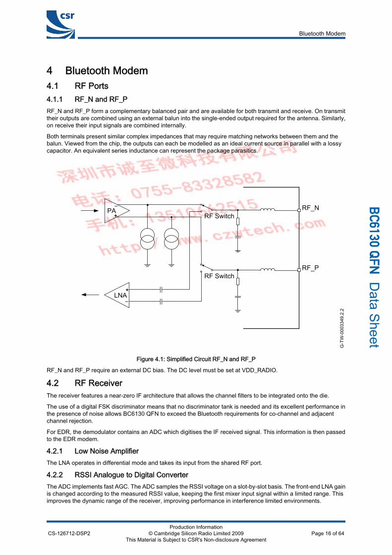
4 Bluetooth Modem4.1 RF Ports4.1.1 RF_N and RF_PRF_N and RF_P form a complementary balanced pair and are available for both transmit and receive. On transmittheir outputs are combined using an external balun into the single-ended output required for the antenna. Similarly,on receive their input signals are combined internally.
Both terminals present similar complex impedances that may require matching networks between them and thebalun. Viewed from the chip, the outputs can each be modelled as an ideal current source in parallel with a lossycapacitor. An equivalent series inductance can represent the package parasitics.
G-T
W-0
0033
49.2
.2
+
_PA
+
_LNA
RF Switch
RF Switch
RF_N
RF_P
Figure 4.1: Simplified Circuit RF_N and RF_P
RF_N and RF_P require an external DC bias. The DC level must be set at VDD_RADIO.
4.2 RF ReceiverThe receiver features a near-zero IF architecture that allows the channel filters to be integrated onto the die.
The use of a digital FSK discriminator means that no discriminator tank is needed and its excellent performance inthe presence of noise allows BC6130 QFN to exceed the Bluetooth requirements for co-channel and adjacentchannel rejection.
For EDR, the demodulator contains an ADC which digitises the IF received signal. This information is then passedto the EDR modem.
4.2.1 Low Noise AmplifierThe LNA operates in differential mode and takes its input from the shared RF port.
4.2.2 RSSI Analogue to Digital ConverterThe ADC implements fast AGC. The ADC samples the RSSI voltage on a slot-by-slot basis. The front-end LNA gainis changed according to the measured RSSI value, keeping the first mixer input signal within a limited range. Thisimproves the dynamic range of the receiver, improving performance in interference limited environments.
Bluetooth Modem
CS-126712-DSP2Production Information
© Cambridge Silicon Radio Limited 2009This Material is Subject to CSR's Non-disclosure Agreement
Page 16 of 64
_`SNPM=n
ck Data Sheet
4.3 RF Transmitter4.3.1 IQ ModulatorThe transmitter features a direct IQ modulator to minimise frequency drift during a transmit timeslot, which resultsin a controlled modulation index. Digital baseband transmit circuitry provides the required spectral shaping.
4.3.2 Power AmplifierThe internal PA has a maximum output power that allows BC6130 QFN to be used in Class 2 and Class 3 radioswithout an external RF PA.
4.4 Bluetooth Radio SynthesiserThe Bluetooth radio synthesiser is fully integrated onto the die with no requirement for an external VCO screeningcan, varactor tuning diodes, LC resonators or loop filter. The synthesiser is guaranteed to lock in sufficient timeacross the guaranteed temperature range to meet the Bluetooth v2.1 + EDR specification.
4.5 Baseband4.5.1 Burst Mode ControllerDuring transmission the BMC constructs a packet from header information previously loaded into memory-mappedregisters by the software and payload data/voice taken from the appropriate ring buffer in the RAM. During reception,the BMC stores the packet header in memory-mapped registers and the payload data in the appropriate ring bufferin RAM. This architecture minimises the intervention required by the processor during transmission and reception.
4.5.2 Physical Layer Hardware EngineDedicated logic performs the following:
Forward error correction Header error control Cyclic redundancy check Encryption Data whitening Access code correlation Audio transcoding
Firmware performs the following voice data translations and operations: A-law/µ-law/linear voice data (from host) A-law/µ-law/CVSD (over the air) Voice interpolation for lost packets Rate mismatch correction
The hardware supports all optional and mandatory features of Bluetooth v2.1 + EDR specification including AFHand eSCO.
4.6 AuriStream CodecThe AuriStream codec is an ADPCM codec and works on the principle of transmitting the difference between theactual value of the signal and a prediction rather than the signal itself. Therefore, the information transmitted isreduced along with the power requirement. The quality of the output depends on the number of bits used to representthe sample.
Note:
The use of the AuriStream codec is as follows: The AuriStream codec is an alternative to standard CVSD It requires CSR devices supporting AuriStream at both ends of the link AuriStream is negotiated when the link is brought up. If AuriStream is not supported on either end, the
system will switch to standard CVSD ensuring full interoperability with any non-AuriStream Bluetoothdevices
The inclusion of the AuriStream codec can greatly enhance audio quality in the wideband mode and results inreduced power consumption compared to a CVSD implementation when used at both ends of the system.
Bluetooth Modem
CS-126712-DSP2Production Information
© Cambridge Silicon Radio Limited 2009This Material is Subject to CSR's Non-disclosure Agreement
Page 17 of 64
_`SNPM=n
ck Data Sheet
AuriStream codec on BC6130 QFN supports only 2 G726 modes of operation which is configured by PSKEY_USR28:1. 4-bit, 8kHz sample rate, 32kbps
Mode 1 gives 30% reduced power in both handset and headset Bluetooth ICs2. 4-bit, 16kHz sample rate, 64kbps
Mode 2 gives wideband voice quality with no power consumption impact compared to standard CVSD
4.7 Basic Rate ModemThe basic rate modem satisfies the basic data rate requirements of the Bluetooth v2.1 + EDR specification. Thebasic rate was the standard data rate available on the Bluetooth v1.2 specification and below, it is based onGFSK modulation scheme.
Including the basic rate modem allows BC6130 QFN compatibility with earlier Bluetooth products.
The basic rate modem uses the RF ports, receiver, transmitter and synthesiser, alongside the baseband componentsdescribed in Section 4.5.
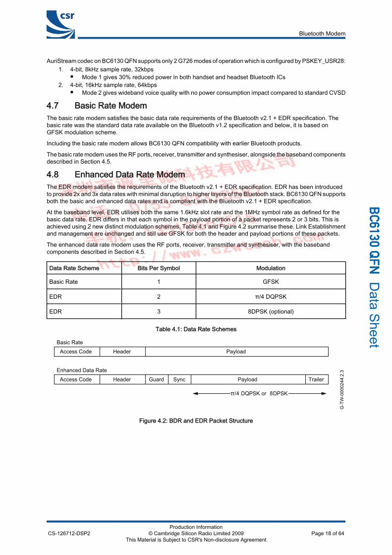
4.8 Enhanced Data Rate ModemThe EDR modem satisfies the requirements of the Bluetooth v2.1 + EDR specification. EDR has been introducedto provide 2x and 3x data rates with minimal disruption to higher layers of the Bluetooth stack. BC6130 QFN supportsboth the basic and enhanced data rates and is compliant with the Bluetooth v2.1 + EDR specification.
At the baseband level, EDR utilises both the same 1.6kHz slot rate and the 1MHz symbol rate as defined for thebasic data rate. EDR differs in that each symbol in the payload portion of a packet represents 2 or 3 bits. This isachieved using 2 new distinct modulation schemes. Table 4.1 and Figure 4.2 summarise these. Link Establishmentand management are unchanged and still use GFSK for both the header and payload portions of these packets.
The enhanced data rate modem uses the RF ports, receiver, transmitter and synthesiser, with the basebandcomponents described in Section 4.5.
Data Rate Scheme Bits Per Symbol Modulation
Basic Rate 1 GFSK
EDR 2 π/4 DQPSK
EDR 3 8DPSK (optional)
Table 4.1: Data Rate Schemes
G-T
W-0
0002
44.2
.3
Access Code
Access Code
Header
Header
Payload
Guard Sync Payload Trailer
Basic Rate
Enhanced Data Rate
/4 DQPSK or 8DPSK
Figure 4.2: BDR and EDR Packet Structure
Bluetooth Modem
CS-126712-DSP2Production Information
© Cambridge Silicon Radio Limited 2009This Material is Subject to CSR's Non-disclosure Agreement
Page 18 of 64
_`SNPM=n
ck Data Sheet
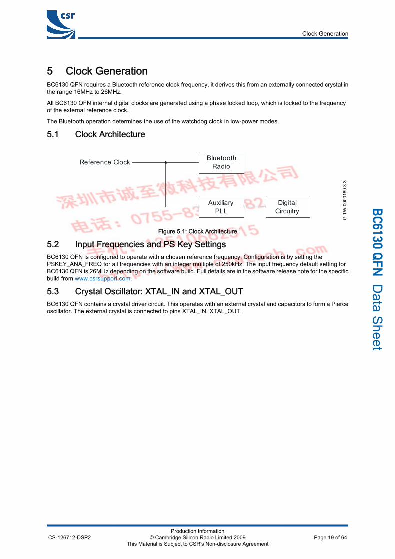
5 Clock GenerationBC6130 QFN requires a Bluetooth reference clock frequency, it derives this from an externally connected crystal inthe range 16MHz to 26MHz.
All BC6130 QFN internal digital clocks are generated using a phase locked loop, which is locked to the frequencyof the external reference clock.
The Bluetooth operation determines the use of the watchdog clock in low-power modes.
5.1 Clock Architecture
G-T
W-0
0001
89.3
.3
Bluetooth Radio
Auxiliary PLL
Digital Circuitry
Reference Clock
Figure 5.1: Clock Architecture
5.2 Input Frequencies and PS Key SettingsBC6130 QFN is configured to operate with a chosen reference frequency. Configuration is by setting thePSKEY_ANA_FREQ for all frequencies with an integer multiple of 250kHz. The input frequency default setting forBC6130 QFN is 26MHz depending on the software build. Full details are in the software release note for the specificbuild from www.csrsupport.com.
5.3 Crystal Oscillator: XTAL_IN and XTAL_OUTBC6130 QFN contains a crystal driver circuit. This operates with an external crystal and capacitors to form a Pierceoscillator. The external crystal is connected to pins XTAL_IN, XTAL_OUT.
Clock Generation
CS-126712-DSP2Production Information
© Cambridge Silicon Radio Limited 2009This Material is Subject to CSR's Non-disclosure Agreement
Page 19 of 64
_`SNPM=n
ck Data Sheet
G-T
W-0
0001
91.3
.2
-
gm
C trim Cint
C t2 C t1
XTAL_OUT
XTAL_IN
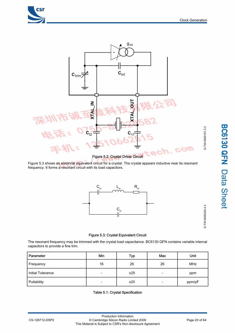
Figure 5.2: Crystal Driver Circuit
Figure 5.3 shows an electrical equivalent circuit for a crystal. The crystal appears inductive near its resonantfrequency. It forms a resonant circuit with its load capacitors.
G-T
W-0
0002
45.4
.4
Lm RmCm
CO
Figure 5.3: Crystal Equivalent Circuit
The resonant frequency may be trimmed with the crystal load capacitance. BC6130 QFN contains variable internalcapacitors to provide a fine trim.
Parameter Min Typ Max Unit
Frequency 16 26 26 MHz
Initial Tolerance - ±25 - ppm
Pullability - ±20 - ppm/pF
Table 5.1: Crystal Specification
Clock Generation
CS-126712-DSP2Production Information
© Cambridge Silicon Radio Limited 2009This Material is Subject to CSR's Non-disclosure Agreement
Page 20 of 64
_`SNPM=n
ck Data Sheet
The BC6130 QFN driver circuit is a transconductance amplifier. A voltage at XTAL_IN generates a current atXTAL_OUT. The value of transconductance is variable and may be set for optimum performance.
5.3.1 Load CapacitanceFor resonance at the correct frequency the crystal should be loaded with its specified load capacitance, which isdefined for the crystal. This is the total capacitance across the crystal viewed from its terminals. BC6130 QFNprovides some of this load with the capacitors Ctrim and Cint. The remainder should be from the external capacitorslabelled Ct1 and Ct2. Ct1 should be three times the value of Ct2 for best noise performance. This maximises the signalswing and slew rate at XTAL_IN (to which all on-chip clocks are referred).
Crystal load capacitance, Cl is calculated with Equation 5.1:
Cl = Cint +(Ct2 + Ctrim) Ct1Ct2 + Ctrim + Ct1
Equation 5.1: Load Capacitance
Note:
Ctrim = 3.4pF nominal (mid-range setting)
Cint = 1.5pF
Cint does not include the crystal internal self capacitance; it is the driver self capacitance.
5.3.2 Frequency TrimBC6130 QFN enables frequency adjustments to be made. This feature is typically used to remove initial tolerancefrequency errors associated with the crystal. Frequency trim is achieved by adjusting the crystal load capacitancewith an on-chip trim capacitor, Ctrim. The value of Ctrim is set by a 6-bit word in the PSKEY_ANA_FTRIM. Its valueis calculated as follows:
Ctrim = 125fF × PSKEY_ANA_FTRIM
Equation 5.2: Trim Capacitance
The Ctrim capacitor is connected between XTAL_IN and ground. When viewed from the crystal terminals, thecombination of the tank capacitors and the trim capacitor presents a load across the terminals of the crystal whichvaries in steps of typically 125fF for each least significant bit increment of PSKEY_ANA_FTRIM.
Equation 5.3 describes the frequency trim.
Δ(Fx)Fx
= pullability × 0.110 × ( Ct1Ct1 + Ct2 + Ctrim )(ppm/LSB)
Equation 5.3: Frequency Trim
Note:
Fx = crystal frequency
Pullability is a crystal parameter with units of ppm/pF
Total trim range is 0 to 63
If not specified, the pullability of a crystal may be calculated from its motional capacitance with Equation 5.4.
( )( ) ( )20II
mXX
CCC 2CFF+
=∂∂
•
Equation 5.4: Pullability
Clock Generation
CS-126712-DSP2Production Information
© Cambridge Silicon Radio Limited 2009This Material is Subject to CSR's Non-disclosure Agreement
Page 21 of 64
_`SNPM=n
ck Data Sheet
Note:
C0 = Crystal self capacitance (shunt capacitance)
Cm = Crystal motional capacitance (series branch capacitance in crystal model), see Figure 5.3
It is a Bluetooth requirement that the frequency is always within ±20ppm. The trim range should be sufficient topull the crystal within ±5ppm of the exact frequency. This leaves a margin of ±15ppm for frequency drift withageing and temperature. A crystal with an ageing and temperature drift specification of better than ±15ppm isrequired.
5.3.3 Transconductance Driver ModelThe crystal and its load capacitors should be viewed as a transimpedance element, whereby a current applied toone terminal generates a voltage at the other. The transconductance amplifier in BC6130 QFN uses the voltage atits input, XTAL_IN, to generate a current at its output, XTAL_OUT. Therefore, the circuit will oscillate if thetransconductance, transimpedance product is greater than unity. For sufficient oscillation amplitude, the productshould be greater than three. The transconductance required for oscillation is defined by the relationship shown inEquation 5.5.
gm > 3(2πFx)2 Rm ((C0 + Cint)(Ct1 + Ct2 + Ctrim) + Ct1 (Ct2 + Ctrim))
Ct1 (Ct2 + Ctrim)
Equation 5.5: Transconductance Required for Oscillation
BC6130 QFN guarantees a transconductance value of at least 2mA/V at maximum drive level.
Note:
More drive strength is required for higher frequency crystals, higher loss crystals (larger Rm) or highercapacitance loading
Optimum drive level is attained when the level at XTAL_IN is approximately 1V pk-pk. The drive level isdetermined by the crystal driver transconductance.
5.3.4 Negative Resistance ModelAn alternative representation of the crystal and its load capacitors is a frequency dependent resistive element. Thedriver amplifier may be considered as a circuit that provides negative resistance. For oscillation, the value of thenegative resistance must be greater than that of the crystal circuit equivalent resistance. Although the BC6130 QFNcrystal driver circuit is based on a transimpedance amplifier, an equivalent negative resistance can be calculatedfor it using Equation 5.6.
Rneg >Ct1(Ct2 + Ctrim)
gm(2πFx)2(C0 + Cint)((Ct1 + Ct2 + Ctrim) + Ct1(Ct2 + Ctrim))2
Equation 5.6: Equivalent Negative Resistance
This formula shows the negative resistance of the BC6130 QFN driver as a function of its drive strength.
The value of the driver negative resistance may be easily measured by placing an additional resistance in serieswith the crystal. The maximum value of this resistor (oscillation occurs) is the equivalent negative resistance of theoscillator.
5.3.5 Crystal PS Key SettingsThe BC6130 QFN firmware automatically controls the drive level on the crystal circuit to achieve optimum inputswing. The PSKEY_XTAL_TARGET_AMPLITUDE is used by the firmware to servo the required amplitude of crystaloscillation. Refer to the software build release note for a detailed description.
BC6130 QFN should be configured to operate with the chosen reference frequency.
5.4 External 32kHz ClockA 32kHz clock can be applied to AIO[0] by setting DEEP_SLEEP_EXTERNAL_CLOCK_SOURCE.
If the external clock is applied to the analogue pad AIO[0], the digital signal should be driven with a maximum 1.5V.
Clock Generation
CS-126712-DSP2Production Information
© Cambridge Silicon Radio Limited 2009This Material is Subject to CSR's Non-disclosure Agreement
Page 22 of 64
_`SNPM=n
ck Data Sheet
Note:
If the 32kHz clock is accurate and stable to within 200ppm, then further power saving features can be enabled.See the relevant software release note for more information.
Clock Generation
CS-126712-DSP2Production Information
© Cambridge Silicon Radio Limited 2009This Material is Subject to CSR's Non-disclosure Agreement
Page 23 of 64
_`SNPM=n
ck Data Sheet
6 Bluetooth Stack MicrocontrollerA 16-bit RISC MCU is used for low power consumption and efficient use of memory.
The MCU, interrupt controller and event timer run the Bluetooth software stack and control the Bluetooth radio andhost interfaces.
6.1 Programmable I/O (PIO) Parallel Ports8 lines of programmable bidirectional I/O are provided.
Note:
PIO[11,3:0] are powered from VDD_PADS[0] and PIO[8:6] are powered from VDD_PADS[1]. AIO[1:0] arepowered from VDD_ANA.
Any of the PIO lines are configurable as button inputs or control outputs. Certain PIOs also have dedicated functionsthat are accessed using appropriate PS Keys. Using PSKEY_CLOCK_REQUEST_ENABLE, PIO[6] or PIO[2] canbe configured as a request line for an external clock source. This is useful in detecting when BC6130 QFN is enteringor leaving deep sleep.
Note:
CSR cannot guarantee that the PIO assignments remain as described. Refer to the relevant software releasenote for the implementation of these PIO lines, as they are firmware build-specific.
BC6130 QFN has 2 general-purpose analogue interface pins, AIO[1:0], used to access internal circuitry and controlsignals. Auxiliary functions available on the analogue interface include a 10-bit ADC. Signals selectable on thisinterface include the band gap reference voltage and a variety of clock signals: 64, 48, 32, 24, 16, 12, 8, 6 and 2MHz(output from AIO[0] only) and the XTAL and XTAL/2 clock frequency (output from AIO[1] and AIO[0]). When usedwith analogue signals the voltage range is constrained by the analogue supply voltage. When configured to driveout digital level signals (clocks) generated from within the analogue part of the device, the output voltage level isdetermined by VDD_ANA.
Bluetooth Stack Microcontroller
CS-126712-DSP2Production Information
© Cambridge Silicon Radio Limited 2009This Material is Subject to CSR's Non-disclosure Agreement
Page 24 of 64
_`SNPM=n
ck Data Sheet
7 Memory Interface and Management7.1 Memory Management UnitThe MMU provides a number of dynamically allocated ring buffers that hold the data that is transferred betweenBC6130 QFN and the air, or the host. The dynamic allocation of memory ensures efficient use of the availableRAM and is performed by a hardware MMU to minimise the overheads on the processor during data/voice transfers.
7.2 System RAM48KB of on-chip RAM supports the RISC MCU and is shared between the ring buffers used to hold voice/data foreach active connection and the general-purpose memory required by the Bluetooth stack.
7.3 Internal ROMInternal ROM is provided for system firmware implementation.
Memory Interface and Management
CS-126712-DSP2Production Information
© Cambridge Silicon Radio Limited 2009This Material is Subject to CSR's Non-disclosure Agreement
Page 25 of 64
_`SNPM=n
ck Data Sheet
8 Serial Interfaces8.1 UART InterfaceBC6130 QFN has a standard UART serial interface that provides a simple communications channel for test anddebug using RS232 protocol.
2 signals implement the UART function, UART_TX and UART_RX. When BC6130 QFN is connected to anotherdigital device, UART_RX and UART_TX transfer data between the 2 devices.
UART configuration parameters, such as baud rate and packet format, are set using BC6130 QFN firmware.
Note:
To communicate with the UART at its maximum data rate using a standard PC, an accelerated serial port adaptercard is required for the PC.
Parameter Possible Values
Baud rate Minimum1200 baud (≤2%Error)
9600 baud (≤1%Error)
Maximum 4Mbaud (≤1%Error)
Flow control None
Parity None, Odd or Even
Number of stop bits 1 or 2
Bits per byte 8
Table 8.1: Possible UART Settings
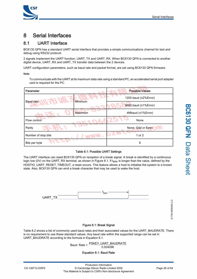
The UART interface can reset BC6130 QFN on reception of a break signal. A break is identified by a continuouslogic low (0V) on the UART_RX terminal, as shown in Figure 8.1. If tBRK is longer than the value, defined by theHOSTIO_UART_RESET_TIMEOUT, a reset occurs. This feature allows a host to initialise the system to a knownstate. Also, BC6130 QFN can emit a break character that may be used to wake the host.
G-T
W-0
0002
50.3
.2 UART_TX
tBRK
Figure 8.1: Break Signal
Table 8.2 shows a list of commonly used baud rates and their associated values for the UART_BAUDRATE. Thereis no requirement to use these standard values. Any baud rate within the supported range can be set inUART_BAUDRATE according to the formula in Equation 8.1.
Baud Rate = PSKEY_UART_BAUDRATE0.004096
Equation 8.1: Baud Rate
Serial Interfaces
CS-126712-DSP2Production Information
© Cambridge Silicon Radio Limited 2009This Material is Subject to CSR's Non-disclosure Agreement
Page 26 of 64
_`SNPM=n
ck Data Sheet
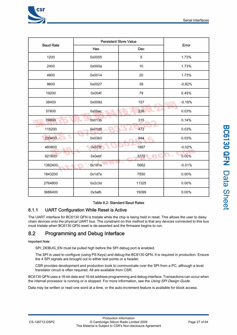
Baud RatePersistent Store Value
ErrorHex Dec
1200 0x0005 5 1.73%
2400 0x000a 10 1.73%
4800 0x0014 20 1.73%
9600 0x0027 39 -0.82%
19200 0x004f 79 0.45%
38400 0x009d 157 -0.18%
57600 0x00ec 236 0.03%
76800 0x013b 315 0.14%
115200 0x01d8 472 0.03%
230400 0x03b0 944 0.03%
460800 0x075f 1887 -0.02%
921600 0x0ebf 3775 0.00%
1382400 0x161e 5662 -0.01%
1843200 0x1d7e 7550 0.00%
2764800 0x2c3d 11325 0.00%
3686400 0x3afb 15099 0.00%
Table 8.2: Standard Baud Rates
8.1.1 UART Configuration While Reset is ActiveThe UART interface for BC6130 QFN is tristate while the chip is being held in reset. This allows the user to daisychain devices onto the physical UART bus. The constraint on this method is that any devices connected to this busmust tristate when BC6130 QFN reset is de-asserted and the firmware begins to run.
8.2 Programming and Debug InterfaceImportant Note:
SPI_DEBUG_EN must be pulled high before the SPI debug port is enabled.
The SPI is used to configure (using PS Keys) and debug the BC6130 QFN. It is required in production. Ensurethe 4 SPI signals are brought out to either test points or a header.
CSR provides development and production tools to communicate over the SPI from a PC, although a leveltranslator circuit is often required. All are available from CSR.
BC6130 QFN uses a 16-bit data and 16-bit address programming and debug interface. Transactions can occur whenthe internal processor is running or is stopped. For more information, see the Using SPI Design Guide.
Data may be written or read one word at a time, or the auto-increment feature is available for block access.
Serial Interfaces
CS-126712-DSP2Production Information
© Cambridge Silicon Radio Limited 2009This Material is Subject to CSR's Non-disclosure Agreement
Page 27 of 64
_`SNPM=n
ck Data Sheet
8.2.1 Instruction CycleThe BC6130 QFN is the slave and receives commands on SPI_MOSI and outputs data on SPI_MISO. Table 8.3shows the instruction cycle for a SPI transaction.
1 Reset the SPI interface Hold SPI_CS# high for two SPI_CLK cycles
2 Write the command word Take SPI_CS# low and clock in the 8-bit command
3 Write the address Clock in the 16-bit address word
4 Write or read data words Clock in or out 16-bit data word(s)
5 Termination Take SPI_CS# high
Table 8.3: Instruction Cycle for a SPI Transaction
With the exception of reset, SPI_CS# must be held low during the transaction. Data on SPI_MOSI is clocked intothe BC6130 QFN on the rising edge of the clock line SPI_CLK. When reading, BC6130 QFN replies to the masteron SPI_MISO with the data changing on the falling edge of the SPI_CLK. The master provides the clock on SPI_CLK.The transaction is terminated by taking SPI_CS# high.
Sending a command word and the address of a register for every time it is to be read or written is a significantoverhead, especially when large amounts of data are to be transferred. To overcome this BC6130 QFN offersincreased data transfer efficiency via an auto increment operation. To invoke auto increment, SPI_CS# is kept low,which auto increments the address, while providing an extra 16 clock cycles for each extra word to be written orread.
8.2.2 Multi-slave OperationBC6130 QFN should not be connected in a multi-slave arrangement by simple parallel connection of slave MISOlines. When BC6130 QFN is deselected (SPI_CS# = 1), the SPI_MISO line does not float. Instead, BC6130 QFNoutputs 0 if the processor is running or 1 if it is stopped.
8.3 I2C InterfacePIO[8:6] is available to form a master I²C interface. The interface is formed using software to drive these lines.
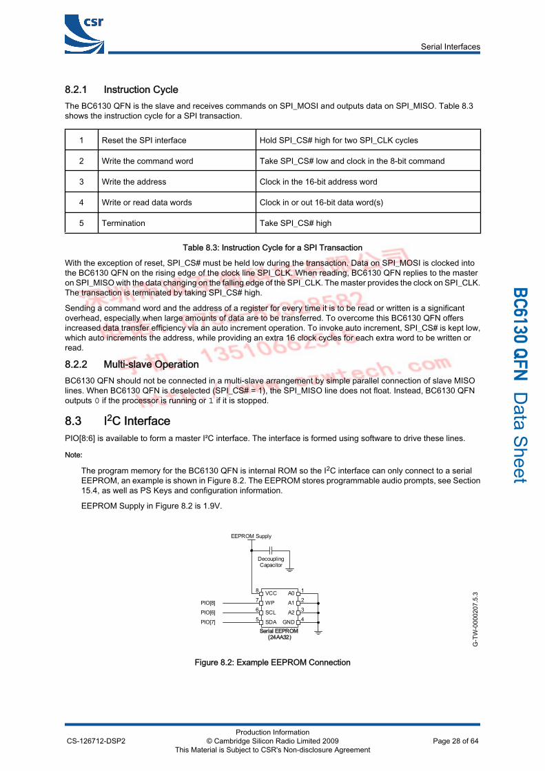
Note:
The program memory for the BC6130 QFN is internal ROM so the I2C interface can only connect to a serialEEPROM, an example is shown in Figure 8.2. The EEPROM stores programmable audio prompts, see Section15.4, as well as PS Keys and configuration information.
EEPROM Supply in Figure 8.2 is 1.9V.
G-T
W-0
0002
07.5
.3
Serial EEPROM(24AA32)
4
3
2
1
5
6
7
8
PIO[8]
PIO[7]
PIO[6]
VCC
WP
SCL
SDA
A0
A1
A2
GND
DecouplingCapacitor
EEPROM Supply
Figure 8.2: Example EEPROM Connection
Serial Interfaces
CS-126712-DSP2Production Information
© Cambridge Silicon Radio Limited 2009This Material is Subject to CSR's Non-disclosure Agreement
Page 28 of 64
_`SNPM=n
ck Data Sheet
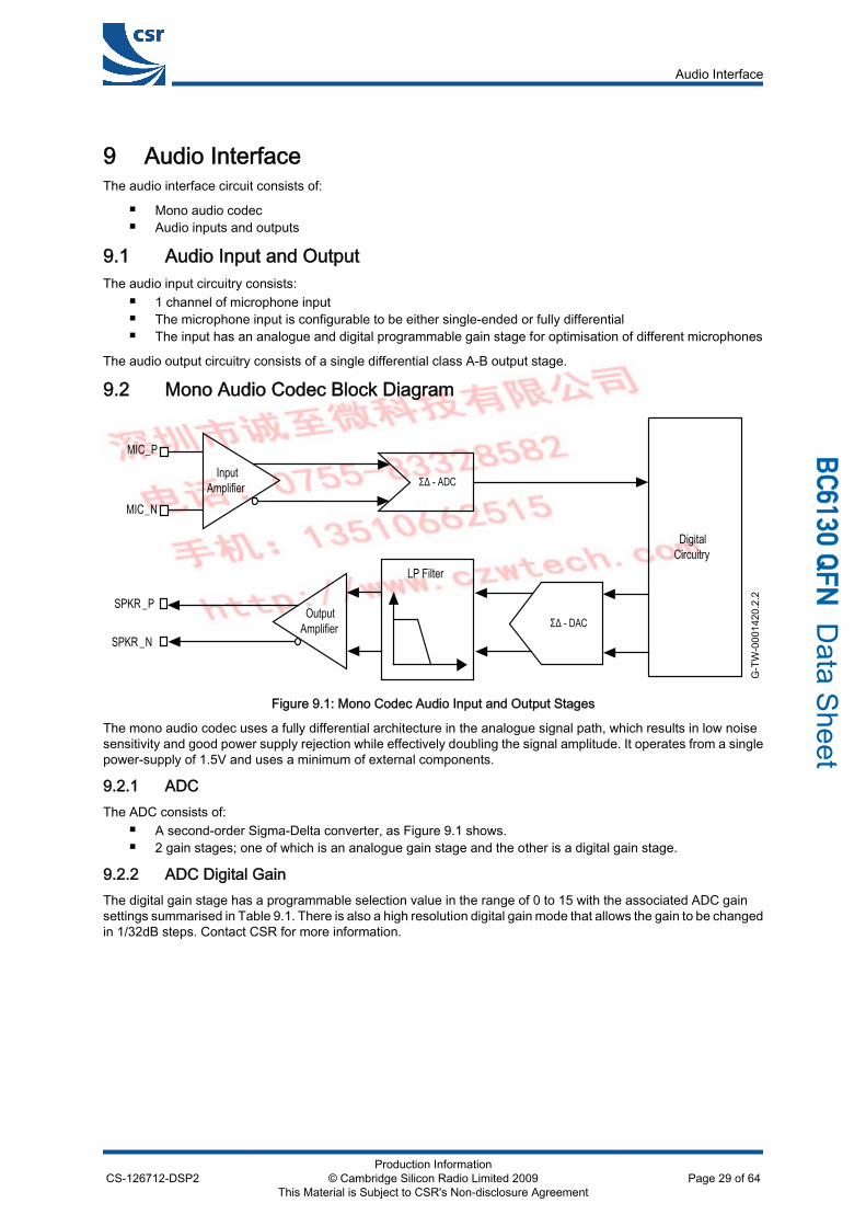
9 Audio InterfaceThe audio interface circuit consists of:
Mono audio codec Audio inputs and outputs
9.1 Audio Input and OutputThe audio input circuitry consists:
1 channel of microphone input The microphone input is configurable to be either single-ended or fully differential The input has an analogue and digital programmable gain stage for optimisation of different microphones
The audio output circuitry consists of a single differential class A-B output stage.
9.2 Mono Audio Codec Block Diagram
G-T
W-0
0014
20.2
.2
MIC_N
MIC_P
SPKR _P
SPKR _N
DigitalCircuitry
Output Amplifier
Input Amplifier
LP Filter
ΣΔ - ADC
ΣΔ - DAC
Figure 9.1: Mono Codec Audio Input and Output Stages
The mono audio codec uses a fully differential architecture in the analogue signal path, which results in low noisesensitivity and good power supply rejection while effectively doubling the signal amplitude. It operates from a singlepower-supply of 1.5V and uses a minimum of external components.
9.2.1 ADCThe ADC consists of:
A second-order Sigma-Delta converter, as Figure 9.1 shows. 2 gain stages; one of which is an analogue gain stage and the other is a digital gain stage.
9.2.2 ADC Digital GainThe digital gain stage has a programmable selection value in the range of 0 to 15 with the associated ADC gainsettings summarised in Table 9.1. There is also a high resolution digital gain mode that allows the gain to be changedin 1/32dB steps. Contact CSR for more information.
Audio Interface
CS-126712-DSP2Production Information
© Cambridge Silicon Radio Limited 2009This Material is Subject to CSR's Non-disclosure Agreement
Page 29 of 64
_`SNPM=n
ck Data Sheet
Gain Selection Value ADC Digital Gain Setting(dB) Gain Selection Value ADC Digital Gain Setting
(dB)
0 0 8 -24
1 3.5 9 -20.5
2 6 10 -18
3 9.5 11 -14.5
4 12 12 -12
5 15.5 13 -8.5
6 18 14 -6
7 21.5 15 -2.5
Table 9.1: ADC Digital Gain Rate Selection
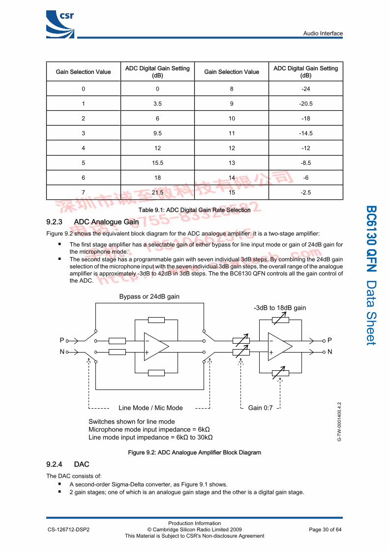
9.2.3 ADC Analogue GainFigure 9.2 shows the equivalent block diagram for the ADC analogue amplifier. It is a two-stage amplifier:
The first stage amplifier has a selectable gain of either bypass for line input mode or gain of 24dB gain forthe microphone mode.
The second stage has a programmable gain with seven individual 3dB steps. By combining the 24dB gainselection of the microphone input with the seven individual 3dB gain steps, the overall range of the analogueamplifier is approximately -3dB to 42dB in 3dB steps. The the BC6130 QFN controls all the gain control ofthe ADC.
G-T
W-0
0014
00.4
.2
Bypass or 24dB gain
Line Mode / Mic Mode
Switches shown for line modeMicrophone mode input impedance = 6kΩLine mode input impedance = 6kΩ to 30kΩ
Gain 0:7
-3dB to 18dB gain
PN
PN
Figure 9.2: ADC Analogue Amplifier Block Diagram
9.2.4 DACThe DAC consists of:
A second-order Sigma-Delta converter, as Figure 9.1 shows. 2 gain stages; one of which is an analogue gain stage and the other is a digital gain stage.
Audio Interface
CS-126712-DSP2Production Information
© Cambridge Silicon Radio Limited 2009This Material is Subject to CSR's Non-disclosure Agreement
Page 30 of 64
_`SNPM=n
ck Data Sheet
9.2.5 DAC Digital GainThe digital gain stage has a programmable selection value in the range of 0 to 15 with associated DAC gain settings,summarised in Table 9.2. There is also a high resolution digital gain mode that allows the gain to be changed in1/32dB steps. Contact CSR for more information.
The overall gain control of the DAC is controlled by the BC6130 QFN. Its setting is a combined function of the digitaland analogue amplifier settings.
Digital Gain SelectionValue
DAC Digital Gain Setting(dB)
Digital Gain SelectionValue
DAC Digital Gain Setting(dB)
0 0 8 -24
1 3.5 9 -20.5
2 6 10 -18
3 9.5 11 -14.5
4 12 12 -12
5 15.5 13 -8.5
6 18 14 -6
7 21.5 15 -2.5
Table 9.2: DAC Digital Gain Rate Selection
9.2.6 DAC Analogue GainAs Table 9.3 shows the DAC analogue gain stage consists of 8 gain selection values that represent seven 3dB steps.
The the BC6130 QFN controls the overall gain control of the DAC. Its setting is a combined function of the digitaland analogue amplifier settings.
Analogue Gain SelectionValue
DAC Analogue GainSetting (dB)
Analogue Gain SelectionValue
DAC Analogue GainSetting (dB)
7 3 3 -9
6 0 2 -12
5 -3 1 -15
4 -6 0 -18
Table 9.3: DAC Analogue Gain Rate Selection
9.2.7 Microphone InputFigure 9.3 shows recommended biasing for each microphone. The microphone bias, MIC_BIAS, derives its powerfrom the BAT_P and requires a 1µF capacitor on its output.
Audio Interface
CS-126712-DSP2Production Information
© Cambridge Silicon Radio Limited 2009This Material is Subject to CSR's Non-disclosure Agreement
Page 31 of 64
_`SNPM=n
ck Data Sheet
G-T
W-0
0011
89.2
.2
R2
C2R1
C1
Microphone Bias
C3
C4
MIC_P
MIC_N
MIC1+
Input Amplifier
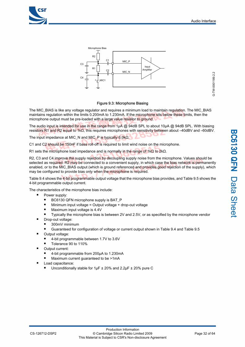
Figure 9.3: Microphone Biasing
The MIC_BIAS is like any voltage regulator and requires a minimum load to maintain regulation. The MIC_BIASmaintains regulation within the limits 0.200mA to 1.230mA. If the microphone sits below these limits, then themicrophone output must be pre-loaded with a large value resistor to ground.
The audio input is intended for use in the range from 1μA @ 94dB SPL to about 10μA @ 94dB SPL. With biasingresistors R1 and R2 equal to 1kΩ, this requires microphones with sensitivity between about –40dBV and –60dBV.
The input impedance at MIC_N and MIC_P is typically 6.0kΩ.
C1 and C2 should be 150nF if bass roll-off is required to limit wind noise on the microphone.
R1 sets the microphone load impedance and is normally in the range of 1kΩ to 2kΩ.
R2, C3 and C4 improve the supply rejection by decoupling supply noise from the microphone. Values should beselected as required. R2 may be connected to a convenient supply, in which case the bias network is permanentlyenabled, or to the MIC_BIAS output (which is ground referenced and provides good rejection of the supply), whichmay be configured to provide bias only when the microphone is required.
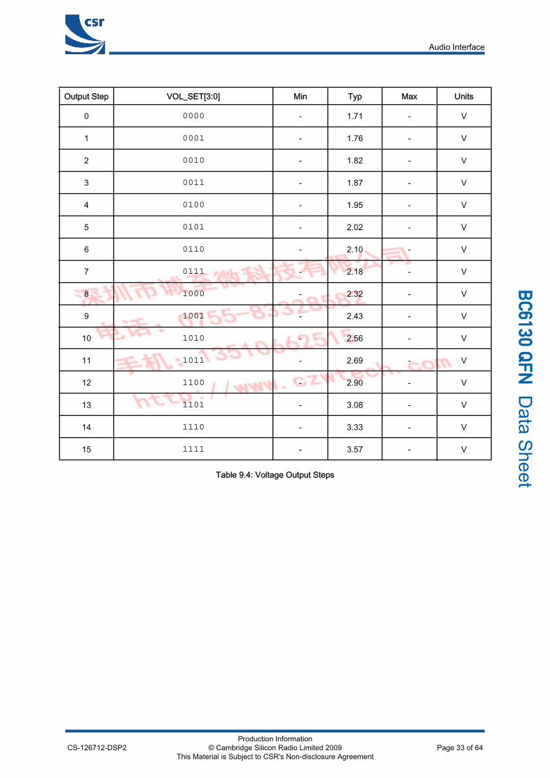
Table 9.4 shows the 4-bit programmable output voltage that the microphone bias provides, and Table 9.5 shows the4-bit programmable output current.
The characteristics of the microphone bias include: Power supply:
BC6130 QFN microphone supply is BAT_P Minimum input voltage = Output voltage + drop-out voltage Maximum input voltage is 4.4V Typically the microphone bias is between 2V and 2.5V, or as specified by the microphone vendor
Drop-out voltage: 300mV minimum Guaranteed for configuration of voltage or current output shown in Table 9.4 and Table 9.5
Output voltage: 4-bit programmable between 1.7V to 3.6V Tolerance 90 to 110%
Output current: 4-bit programmable from 200µA to 1.230mA Maximum current guaranteed to be >1mA
Load capacitance: Unconditionally stable for 1µF ± 20% and 2.2µF ± 20% pure C
Audio Interface
CS-126712-DSP2Production Information
© Cambridge Silicon Radio Limited 2009This Material is Subject to CSR's Non-disclosure Agreement
Page 32 of 64
_`SNPM=n
ck Data Sheet
Output Step VOL_SET[3:0] Min Typ Max Units
0 0000 - 1.71 - V
1 0001 - 1.76 - V
2 0010 - 1.82 - V
3 0011 - 1.87 - V
4 0100 - 1.95 - V
5 0101 - 2.02 - V
6 0110 - 2.10 - V
7 0111 - 2.18 - V
8 1000 - 2.32 - V
9 1001 - 2.43 - V
10 1010 - 2.56 - V
11 1011 - 2.69 - V
12 1100 - 2.90 - V
13 1101 - 3.08 - V
14 1110 - 3.33 - V
15 1111 - 3.57 - V
Table 9.4: Voltage Output Steps
Audio Interface
CS-126712-DSP2Production Information
© Cambridge Silicon Radio Limited 2009This Material is Subject to CSR's Non-disclosure Agreement
Page 33 of 64
_`SNPM=n
ck Data Sheet
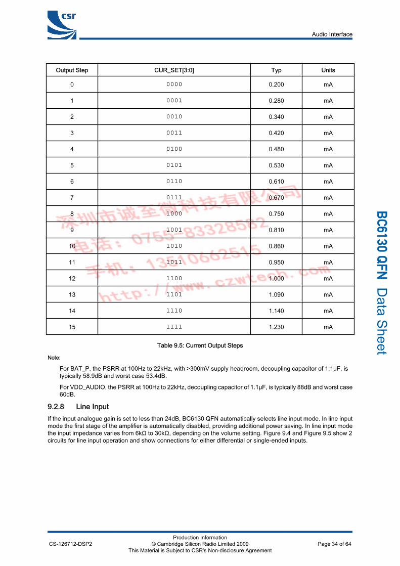
Output Step CUR_SET[3:0] Typ Units
0 0000 0.200 mA
1 0001 0.280 mA
2 0010 0.340 mA
3 0011 0.420 mA
4 0100 0.480 mA
5 0101 0.530 mA
6 0110 0.610 mA
7 0111 0.670 mA
8 1000 0.750 mA
9 1001 0.810 mA
10 1010 0.860 mA
11 1011 0.950 mA
12 1100 1.000 mA
13 1101 1.090 mA
14 1110 1.140 mA
15 1111 1.230 mA
Table 9.5: Current Output Steps
Note:
For BAT_P, the PSRR at 100Hz to 22kHz, with >300mV supply headroom, decoupling capacitor of 1.1μF, istypically 58.9dB and worst case 53.4dB.
For VDD_AUDIO, the PSRR at 100Hz to 22kHz, decoupling capacitor of 1.1μF, is typically 88dB and worst case60dB.
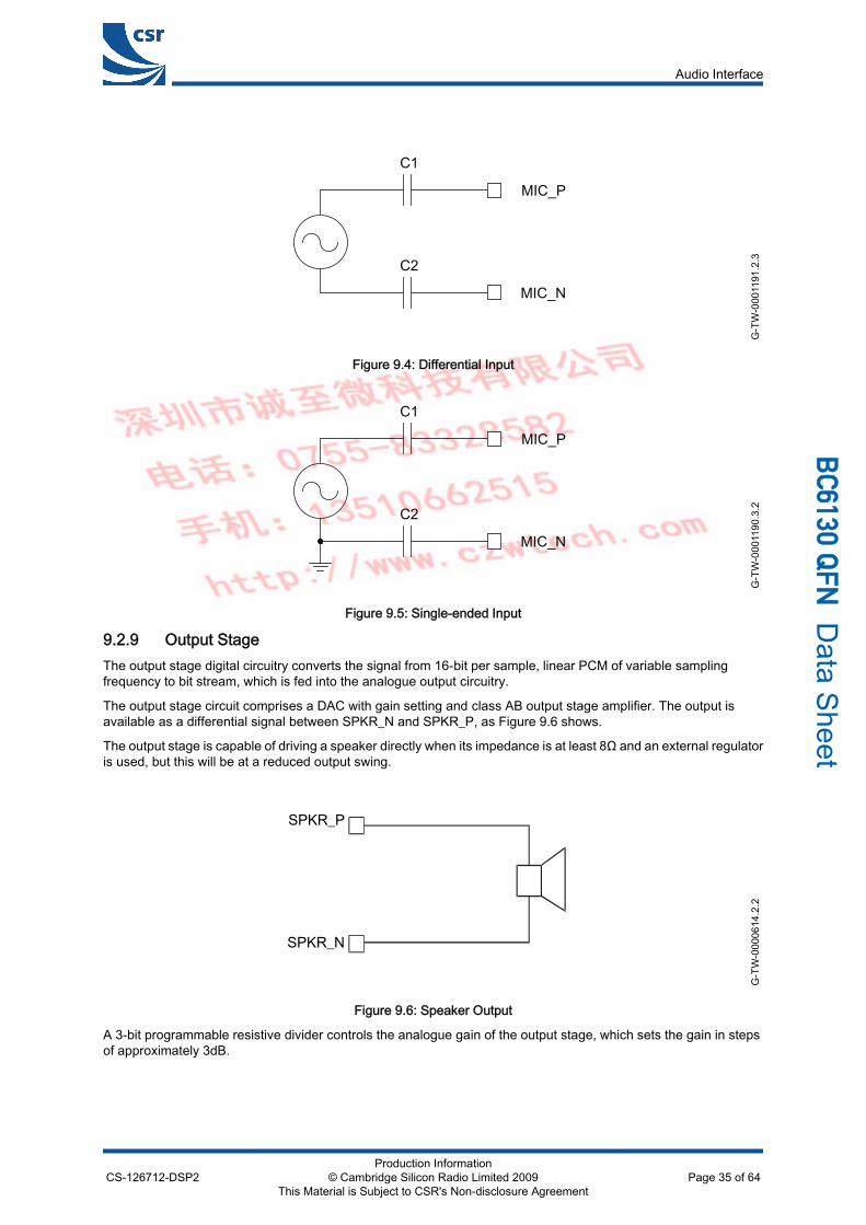
9.2.8 Line InputIf the input analogue gain is set to less than 24dB, BC6130 QFN automatically selects line input mode. In line inputmode the first stage of the amplifier is automatically disabled, providing additional power saving. In line input modethe input impedance varies from 6kΩ to 30kΩ, depending on the volume setting. Figure 9.4 and Figure 9.5 show 2circuits for line input operation and show connections for either differential or single-ended inputs.
Audio Interface
CS-126712-DSP2Production Information
© Cambridge Silicon Radio Limited 2009This Material is Subject to CSR's Non-disclosure Agreement
Page 34 of 64
_`SNPM=n
ck Data Sheet
G-T
W-0
0011
91.2
.3
C1
C2
MIC_P
MIC_N
Figure 9.4: Differential Input
G-T
W-0
0011
90.3
.2
C1
C2
MIC_P
MIC_N
Figure 9.5: Single-ended Input
9.2.9 Output StageThe output stage digital circuitry converts the signal from 16-bit per sample, linear PCM of variable samplingfrequency to bit stream, which is fed into the analogue output circuitry.
The output stage circuit comprises a DAC with gain setting and class AB output stage amplifier. The output isavailable as a differential signal between SPKR_N and SPKR_P, as Figure 9.6 shows.
The output stage is capable of driving a speaker directly when its impedance is at least 8Ω and an external regulatoris used, but this will be at a reduced output swing.
G-T
W-0
0006
14.2
.2
SPKR_P
SPKR_N
Figure 9.6: Speaker Output
A 3-bit programmable resistive divider controls the analogue gain of the output stage, which sets the gain in stepsof approximately 3dB.
Audio Interface
CS-126712-DSP2Production Information
© Cambridge Silicon Radio Limited 2009This Material is Subject to CSR's Non-disclosure Agreement
Page 35 of 64
_`SNPM=n
ck Data Sheet
9.2.10 Integrated Digital FilterBC6130 QFN has a programmable digital filter integrated into the ADC channel of the codec. The filter is a 2 stage,second order IIR and is used for functions such as custom wind noise rejection. The filter also has optional DCblocking.
The filter has 10 configuration words used as follows: 1 for gain value 8 for coefficient values 1 for enabling and disabling the DC blocking
The gain and coefficients are all 12-bit 2's complement signed integer with the format XX.XXXXXXXXXX
Note:
The position of the binary point is between bit[10] and bit[9], where bit[11] is the most significant bit.
For example:
01.1111111111 = most positive number, close to 2
01.0000000000 = 1
00.0000000000 = 0
11.0000000000 = -1
10.0000000000 = -2, most negative number
Equation 9.1 shows the equation for the IIR filter. Equation 9.2 shows the equation for when the DC blocking isenabled.
The filter can be configured, enabled and disabled from the VM via the CodecSetIIRFilterA andCodecSetIIRFilterB traps. This requires firmware support. The configuration function takes 10 variables inthe order shown below:
0 : Gain
1 : b01
2 : b02
3 : a01
4 : a02
5 : b11
6 : b12
7 : a11
8 : a12
9 : DC Block (1 = enable, 0 = disable)
Audio Interface
CS-126712-DSP2Production Information
© Cambridge Silicon Radio Limited 2009This Material is Subject to CSR's Non-disclosure Agreement
Page 36 of 64
_`SNPM=n
ck Data Sheet
Filter, H(z) = Gain ×( 1 + b01 z−1 + b02 z−2 )
( 1 + a01 z−1 + a02 z−2 )×
( 1 + b11 z−1 + b12 z−2 )
( 1 + a11 z−1 + a12 z−2 )
Equation 9.1: IIR Filter Transfer Function, H(z)
Filter with DC Blocking, HDC (z) = H(z) × ( 1 − z−1 )
Equation 9.2: IIR Filter plus DC Blocking Transfer Function, HDC(z)
9.2.10.1 Integrated Digital Filter ConfigurationThe behaviour of the integrated digital IIR filter described in Section 9.2.10, is configurable through 12 values storedin the PSKEY_USR29:
10-words for the IIR filter parameters in Section 9.2.10 1-word for the audio energy estimation threshold 1-word for the gain to be applied when the audio energy estimation is above the threshold
Adjusting these values configures the IIR filter for different functions: Echo reduction, see Section 9.2.10.2 Noise reduction (wind noise filter), see Section 9.2.10.3
Note:
The IIR filter is switched off at initialisation.
9.2.10.2 Echo ReductionThe echo reduction feature on BC6130 QFN uses the integrated digital IIR filter in Section 9.2.10.
In order to implement the echo reduction feature the energy estimation of the SCO connections is constantlymonitored. When the energy estimation goes above a given threshold, the IIR filter is switched on. When the energyestimation goes below a given threshold, the IIR filter is switched off. Additionally, the echo reduction gain is appliedto the filter.
9.2.10.3 Noise ReductionThe noise reduction feature on BC6130 QFN uses the integrated digital IIR filter in Section 9.2.10 to create a windnoise filter.
The wind noise filter is basically a high-pass filter that is always on. To achieve this: The filter threshold is set to 0 The filter echo reduction gain is set to 0 The filter coefficients are left at their default values
However, it is possible to calculate values for a custom configuration using the filter equation, see Equation 9.1 andEquation 9.2.
9.2.11 Side ToneIn some applications it is necessary to implement side tone. This involves feeding an attenuated version of themicrophone signal to the earpiece. The BC6130 QFN codec contains side tone circuitry to do this. The side tonehardware is configured through the following PS Keys:
PSKEY_SIDE_TONE_ENABLE PSKEY_SIDE_TONE_GAIN PSKEY_SIDE_TONE_AFTER_ADC PSKEY_SIDE_TONE_AFTER_DAC
Audio Interface
CS-126712-DSP2Production Information
© Cambridge Silicon Radio Limited 2009This Material is Subject to CSR's Non-disclosure Agreement
Page 37 of 64
_`SNPM=n
ck Data Sheet

10 Power Control and RegulationBC6130 QFN contains 3 regulators:
A switch-mode regulator, used to generate a 1.5V rail A low-voltage regulator which can generate an optional 1.5V rail A high-voltage linear regulator used to generate a 1.9V rail for powering the EEPROM
Various configurations for power control and regulation with BC6130 QFN are available, but a typical configurationis shown in Figure 10.1. This configuration has the switch-mode regulator generating a 1.5V supply rail, and thehigh-voltage linear regulator creating a 1.9V supply rail.
G-T
W-0
0009
52.4
.2
VREGENABLE_L
VREGIN_L
VREGIN_H
VREGOUT_H
VREGENABLE_H
VSSBAT_P
VDD_CHG
SMP_SENSE
VDD_ANA
LX
High-voltage Linear Regulator
OUT
IN
EN
SENSE
Switch-mode Regulator
SENSEEN
LX
Battery Charger
OUT
IN
1.9 V Rail
VDD_RADIO
VDD_LO
VDD_CORE
VDD_AUDIO
1.5 V Rail
VDD_PADS[1:0]
Battery Supply
Figure 10.1: Voltage Regulator Configuration
10.1 Power SequencingThe 1.5V supply rails are VDD_ANA, VDD_AUDIO, VDD_CORE, VDD_LO and VDD_RADIO. CSR recommendsthat these supply rails are all powered at the same time.
The digital I/O supply rails are VDD_PADS[1:0].
The sequence of powering the 1.5V supply rails relative to the digital I/O supply rails is not important. If the digitalI/O supply rails are powered before the 1.5V supply rails, all digital I/Os will have a weak pull-down irrespective ofthe reset state.
VDD_ANA, VDD_AUDIO, VDD_LO and VDD_RADIO can connect directly to a 1.5V supply.
A simple RC filter is recommended for VDD_CORE to reduce transients fed back onto the power supply rails.
The digital I/O supply rails are connected either together or independently to an appropriate voltage rail. Decouplingof the digital I/O supply rails is recommended.
10.2 External Voltage SourceIf any of the supply rails for BC6130 QFN are supplied from an external voltage source, rather than one of the internalvoltage regulators, CSR recommends that VDD_AUDIO, VDD_LO and VDD_RADIO should have less than 10mVrms noise levels between 0 and 10MHz. Also avoid single tone frequencies.
Power Control and Regulation
CS-126712-DSP2Production Information
© Cambridge Silicon Radio Limited 2009This Material is Subject to CSR's Non-disclosure Agreement
Page 38 of 64
_`SNPM=n
ck Data Sheet
The transient response of any external regulator used should match or be better than the internal regulator availableon BC6130 QFN. For more information, refer to regulator characteristics in Section 12. It is essential that the powerrail recovers quickly at the start of a packet, where the power consumption jumps to high levels.
10.3 Switch-mode RegulatorCSR recommends the on-chip switch-mode regulator to power the 1.5V supply rail.
An external LC filter circuit of a low-resistance series inductor, L1 (22µH), followed by a low ESR shunt capacitor,C1 (4.7µF), is required between the LX terminal and the 1.5V supply rail. A connection between the 1.5V supply railand the SMP_SENSE pin is required.
A 2.2µF decoupling capacitor is required between BAT_P and VSS.
To maintain high-efficiency power conversion and low supply ripple, it is essential that the series resistance of tracksbetween the BAT_P and VSS terminals, the filter and decoupling components, and the external voltage source areminimised.
The switch-mode regulator is enabled by either: VREGENABLE_H pin BC6130 QFN device firmware BC6130 QFN battery charger
The switch-mode regulator switches into a low-power pulse skipping mode when the device is sent into deep sleepmode, or in reset.
When the switch-mode regulator is not required the terminals BAT_P and LX must be grounded or left unconnected.
10.4 High-voltage Linear RegulatorThe 1.9V high-voltage linear regulator provides power for an external EEPROM. The external EEPROM storesPS Key and configuration information, see Section 8.3. CSR does not recommend using the high-voltage linearregulator to power any additional circuitry.
A smoothing circuit using a low ESR 2.2µF capacitor and a 2.2Ω resistor to ground, should be connected to theoutput of the high-voltage linear regulator, VREGOUT_H. Alternatively use a 2.2µF capacitor with an ESR of at least2Ω.
The high-voltage linear regulator is enabled by either: VREGENABLE_H pin BC6130 QFN device firmware BC6130 QFN battery charger
The regulator is switched into a low-power mode when the device is in deep sleep mode, or in reset.
10.5 Low-voltage Linear RegulatorThe low-voltage linear regulator is available to power a 1.5V supply rail. Its output is connected internally toVDD_ANA, and can be connected externally to the other 1.5V power inputs.
If the low-voltage linear regulator is used, connect a smoothing circuit using a low ESR 2.2µF capacitor and a2.2Ω resistor to ground to the output of the low-voltage linear regulator, VDD_ANA. Alternatively use a 2.2µFcapacitor with an ESR of at least 2Ω.
The low-voltage linear regulator is enabled by either: VREGENABLE_L pin BC6130 QFN device firmware BC6130 QFN battery charger
The low-voltage linear regulator switches into a low power mode when the device is in deep sleep mode, or in reset.
When the low-voltage linear regulator is not used, either leave the terminal VREGIN_L unconnected, or tie it toVDD_ANA.
10.6 Voltage Regulator Enable PinsThe voltage regulator enable pins, VREGENABLE_H and VREGENABLE_L, are used to enable the BC6130 QFNdevice if the on-chip regulators are being used. Table 10.1 shows the enable pin responsible for each voltageregulator.
Power Control and Regulation
CS-126712-DSP2Production Information
© Cambridge Silicon Radio Limited 2009This Material is Subject to CSR's Non-disclosure Agreement
Page 39 of 64
_`SNPM=n
ck Data Sheet
Enable Pin Regulator
VREGENABLE_H High-voltage Linear Regulator and Switch-mode Regulator
VREGENABLE_L Low-voltage Linear Regulator
Table 10.1: BC6130 QFN Voltage Regulator Enable Pins
The voltage regulator enable pins are active high, with weak pull-downs.
BC6130 QFN boots-up when the voltage regulator enable pins are pulled high, enabling the appropriate regulators.The firmware then latches the regulators on and the voltage regulator enable pins may then be released.
The status of the VREGENABLE_H pin is available to firmware through an internal connection. VREGENABLE_Halso works as an input line.
10.7 Battery ChargerThe battery charger is a constant current / constant voltage charger circuit, and is suitable for lithium ion/polymerbatteries only. It shares a connection to the battery terminal, BAT_P, with the switch-mode regulator. However it maybe used in conjunction with either of the high-voltage regulators on the device.
The constant current level can be varied to allow charging of different capacity batteries.
The charger enters various states of operation as it charges a battery, as listed below. A full operational descriptionis in BlueCore5 Charger Description and Calibration Procedure Application Note:
Off : entered when charger disconnected. Trickle charge: entered when battery is below 2.9V. The battery is charged at a nominal 4.5mA. This mode
is for the safe charge of deeply discharged cells. Fast charge constant current: entered when battery is above 2.9V. The charger enters the main fast charge
mode. This mode charges the battery at the selected constant current, Ichgset. Fast charge constant voltage: entered when battery has reached a selected voltage, Vfloat. The charger
switches mode to maintain the cell voltage at the Vfloat voltage by adjusting the charge current. Standby: this is the state when the battery is fully charged and no charging takes place. The battery voltage
is continuously monitored and if it drops by more than 150mV below the Vfloat voltage the charger will re-enter the fast charge constant current mode to keep the battery fully charged.
When a voltage is applied to the charger input terminal VDD_CHG, and the battery is not fully charged, the chargeroperates and an LED connected to the terminal LED[0] illuminates. By default, until the firmware is running, theLED pulses at a low-duty cycle to minimise current consumption.
The battery charger circuitry auto-detects the presence of a power source, allowing the firmware to detect, using aninternal status bit, when the charger is powered. Therefore when the charger supply is not connected to VDD_CHG,the terminal must be left open-circuit. The VDD_CHG pin when not connected must be allowed to float and not pulledto a power rail. When the battery charger is not enabled this pin may float to a low undefined voltage. Any DCconnection increases current consumption of the device. Capacitive components may be connected such as diodes,FETs and ESD protection.
The battery charger is designed to operate with a permanently connected battery. If the application enables thecharger input to be connected while the battery is disconnected, then the BAT_P pin voltage may become unstable.This in turn may cause damage to the internal switch-mode regulator. Connecting a 470µF capacitor to BAT_P limitsthese oscillations so preventing damage.
10.8 LED DriversBC6130 QFN includes 2 pads dedicated to driving LED indicators. Both terminals can be controlled by firmware,while LED[0] can also be set by the battery charger.
The terminals are open-drain outputs, so the LED must be connected from a positive supply rail to the pad in serieswith a current limiting resistor.
CSR recommends that the LED pad, LED[0] or LED[1] pins, operate with a pad voltage below 0.5V. In this case,the pad is like a resistor, RON. The resistance together with the external series resistor sets the current, ILED, in theLED. The current is also dependent on the external voltage, VDD, as Figure 10.2 shows.
Power Control and Regulation
CS-126712-DSP2Production Information
© Cambridge Silicon Radio Limited 2009This Material is Subject to CSR's Non-disclosure Agreement
Page 40 of 64
_`SNPM=n
ck Data Sheet
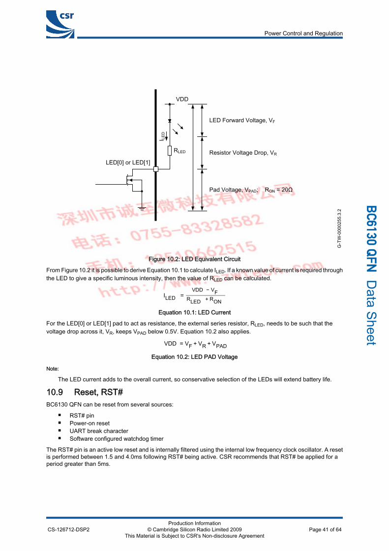
G-T
W-0
0002
55.3
.2
LED Forward Voltage, VF
Pad Voltage, VPAD; RON = 20Ω
RLED
LED[0] or LED[1]Resistor Voltage Drop, VR
VDD
I LED
Figure 10.2: LED Equivalent Circuit
From Figure 10.2 it is possible to derive Equation 10.1 to calculate ILED. If a known value of current is required throughthe LED to give a specific luminous intensity, then the value of RLED can be calculated.
ILED =VDD − VF
RLED + RON
Equation 10.1: LED Current
For the LED[0] or LED[1] pad to act as resistance, the external series resistor, RLED, needs to be such that thevoltage drop across it, VR, keeps VPAD below 0.5V. Equation 10.2 also applies.
VDD = VF + VR + VPAD
Equation 10.2: LED PAD Voltage
Note:
The LED current adds to the overall current, so conservative selection of the LEDs will extend battery life.
10.9 Reset, RST#BC6130 QFN can be reset from several sources:
RST# pin Power-on reset UART break character Software configured watchdog timer
The RST# pin is an active low reset and is internally filtered using the internal low frequency clock oscillator. A resetis performed between 1.5 and 4.0ms following RST# being active. CSR recommends that RST# be applied for aperiod greater than 5ms.
Power Control and Regulation
CS-126712-DSP2Production Information
© Cambridge Silicon Radio Limited 2009This Material is Subject to CSR's Non-disclosure Agreement
Page 41 of 64
_`SNPM=n
ck Data Sheet
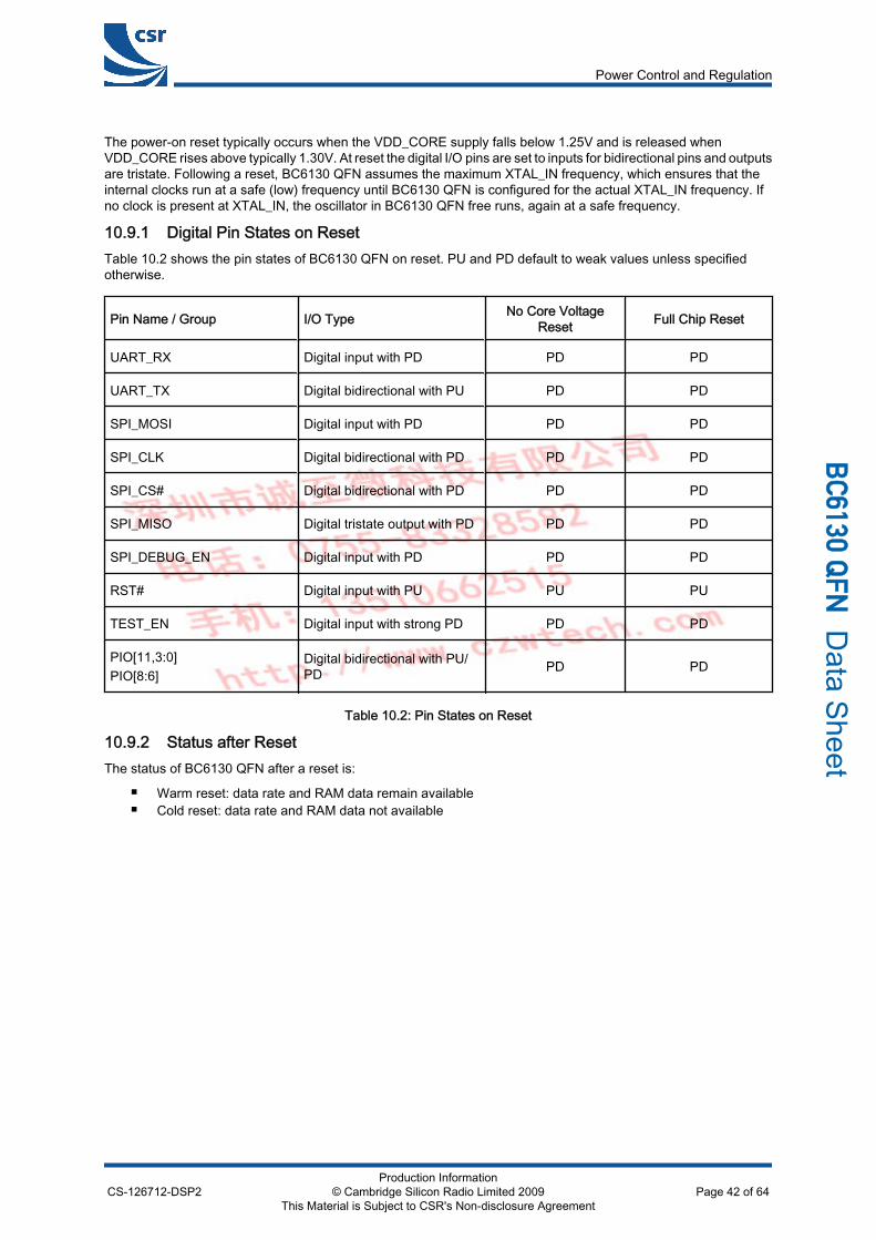
The power-on reset typically occurs when the VDD_CORE supply falls below 1.25V and is released whenVDD_CORE rises above typically 1.30V. At reset the digital I/O pins are set to inputs for bidirectional pins and outputsare tristate. Following a reset, BC6130 QFN assumes the maximum XTAL_IN frequency, which ensures that theinternal clocks run at a safe (low) frequency until BC6130 QFN is configured for the actual XTAL_IN frequency. Ifno clock is present at XTAL_IN, the oscillator in BC6130 QFN free runs, again at a safe frequency.
10.9.1 Digital Pin States on ResetTable 10.2 shows the pin states of BC6130 QFN on reset. PU and PD default to weak values unless specifiedotherwise.
Pin Name / Group I/O Type No Core VoltageReset Full Chip Reset
UART_RX Digital input with PD PD PD
UART_TX Digital bidirectional with PU PD PD
SPI_MOSI Digital input with PD PD PD
SPI_CLK Digital bidirectional with PD PD PD
SPI_CS# Digital bidirectional with PD PD PD
SPI_MISO Digital tristate output with PD PD PD
SPI_DEBUG_EN Digital input with PD PD PD
RST# Digital input with PU PU PU
TEST_EN Digital input with strong PD PD PD
PIO[11,3:0]PIO[8:6]
Digital bidirectional with PU/PD PD PD
Table 10.2: Pin States on Reset
10.9.2 Status after ResetThe status of BC6130 QFN after a reset is:
Warm reset: data rate and RAM data remain available Cold reset: data rate and RAM data not available
Power Control and Regulation
CS-126712-DSP2Production Information
© Cambridge Silicon Radio Limited 2009This Material is Subject to CSR's Non-disclosure Agreement
Page 42 of 64
_`SNPM=n
ck Data Sheet
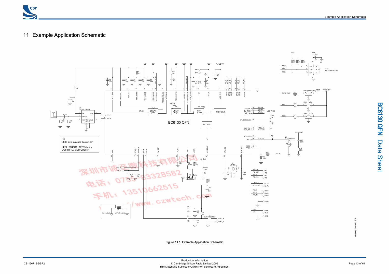
11 Example Application Schematic
G-T
W-0
0043
22.2
.2
15nL1
22nC2
2u2C4
15pC3
2R2R1
1V5
47nC5
100nC6
1V9
22uL2
4u7C7
1V5
1V5
GND
10u
C8
VBAT
BAT-
BAT+
V_CHARGE
4u7C9
10n
C19
4K7R6
4K7R7
4K7R8
PIO_6
PIO_7
PIO_8
1V9 1V9
VSS
4
SDA5
VCC
8
SCL6
WP7 nc 3nc 2nc 1
U31V9
18pC11
26MHz
1 3
24
XT1
6p8C10
10k
R11
10k
R10PIO_1
PIO_2
VDD_PADS
10k
R9PWR/HOLD
1 2
3
SW2 [VOL+]
1 2
3
SW3 [VOL-]
VBAT
1 2
3
SW1 [PWR/HOOK]
VBAT
510RR3
820RR2
LD1
22nC13
47nC14
MIC_BIAS
2u2
C12SPK_N
SPK_P
MIC_N
MIC_P150n
C15
150n
C16
2k2R4
15pC22
PIO
_6PI
O_7
PIO
_8
PIO
_1PI
O_2
PIO
_0
PIO
_3
PIO
_11
PS_CLKPS_OUTPS_INPS_CSB
UART_TXUART_RX
RESETB
0R
C101
NFL101
8n2L102
PCPOPIPS
PS_CLKPS_OUTPS_INPS_CSB
UART_TXUART_RX
U_TxU_Rx
PIO_0 PIO0PIO_3 PIO3PIO_11 PIO11
V_CHARGE
RST
NTA4001NT1G
s
d
g
Q1
220kR12
220nC20
Connect all at STAR point to
NF0201
R999
DBF81F104-CSR
UNBAL1
NC3
DC2
GN
D5
GN
D8
GN
D7
BAL 6
BAL 4
U2
GND2
PWR
/HO
LD
2R2R19
2u2C21
VBAT
VDD_PADS
NFR20
NFR21
0402
100kTH1 100k
R22 PIO_3
1V51V91V9
1V5
Blue
Red
VDD
_PAD
S
15pC17
15pC18
ST MicroM24C32-FMB, UFDFPN8
15pC23
15pC1
BLM15HB221SN1L3
U20805 size matched balun-filter
LFB212G45BA1A220/MurataDBF81F107-CSR/SOSHIN
2u2
C24
1KR5
VDD
_PAD
S[1]
43
SPI_DEBUG_EN 42
AIO[0] 17
SMP_
SEN
SE34
RST# 26
VDD
_PAD
S[0]
20
PIO
[11]
27
PIO
[3]
21PI
O[2
]22
SPI_MISO 41
AIO[1] 16
SPI_CLK 39
SPI_MOSI 38SPI_CS# 40
PIO
[0]
24PI
O[1
]23
PIO
[6]
46
AU_R
EF5
UART_TX 19UART_RX 18
BAT_
P36
VREG
OU
T_H
31
SPKR
_P4
RF_P7
RF_N8
TEST_EN 25
SPKR
_N3
VDD
_LO
9
VDD
_RAD
IO6
LED
[1]
28
VDD
_AN
A12
XTAL
_IN
13
BC6130 QFN
VREG
IN_H
32
VREG
IN_L
11VR
EGEN
ABLE
_L10
LO_R
EF15
VDD
_CO
RE
30
VSS
49
VDD
_AU
DIO
48
LED
[0]
29
(Low)LINEAR
LX35
MIC
_P1
MIC
_N2
VDD
_CH
G37
PIO
[7]
45PI
O[8
]44
XTAL
_OU
T14
VREG
ENAB
LE_H
33
MIC
_BIA
S47
MIC BIAS
(1V5) CHARGERLINEAR(High)
(1V9)
SMP(Low)
(1V5)
U1
Figure 11.1: Example Application Schematic
Example Application Schematic
CS-126712-DSP2Production Information
© Cambridge Silicon Radio Limited 2009This Material is Subject to CSR's Non-disclosure Agreement
Page 43 of 64
_`SNPM=n
ck Data Sheet
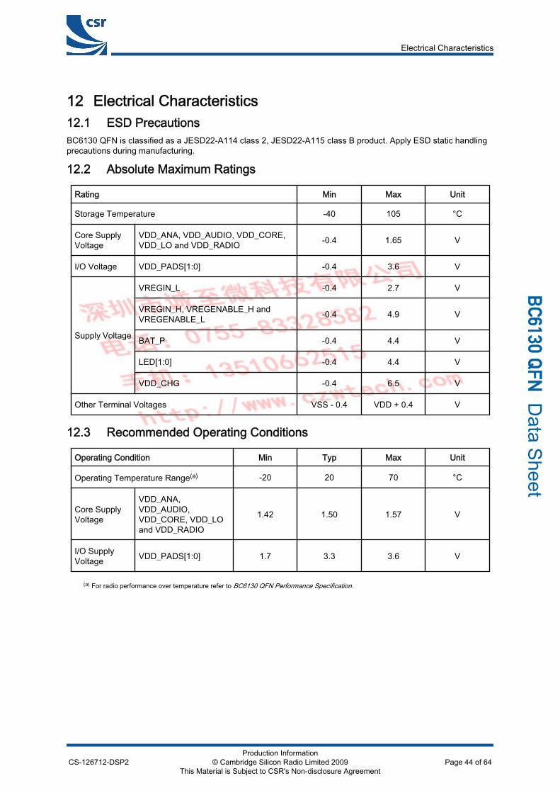
12 Electrical Characteristics12.1 ESD PrecautionsBC6130 QFN is classified as a JESD22-A114 class 2, JESD22-A115 class B product. Apply ESD static handlingprecautions during manufacturing.
12.2 Absolute Maximum Ratings
Rating Min Max Unit
Storage Temperature -40 105 °C
Core SupplyVoltage
VDD_ANA, VDD_AUDIO, VDD_CORE,VDD_LO and VDD_RADIO -0.4 1.65 V
I/O Voltage VDD_PADS[1:0] -0.4 3.6 V
Supply Voltage
VREGIN_L -0.4 2.7 V
VREGIN_H, VREGENABLE_H andVREGENABLE_L -0.4 4.9 V
BAT_P -0.4 4.4 V
LED[1:0] -0.4 4.4 V
VDD_CHG -0.4 6.5 V
Other Terminal Voltages VSS - 0.4 VDD + 0.4 V
12.3 Recommended Operating Conditions
Operating Condition Min Typ Max Unit
Operating Temperature Range(a) -20 20 70 °C
Core SupplyVoltage
VDD_ANA,VDD_AUDIO,VDD_CORE, VDD_LOand VDD_RADIO
1.42 1.50 1.57 V
I/O SupplyVoltage VDD_PADS[1:0] 1.7 3.3 3.6 V
(a) For radio performance over temperature refer to BC6130 QFN Performance Specification.
Electrical Characteristics
CS-126712-DSP2Production Information
© Cambridge Silicon Radio Limited 2009This Material is Subject to CSR's Non-disclosure Agreement
Page 44 of 64
_`SNPM=n
ck Data Sheet
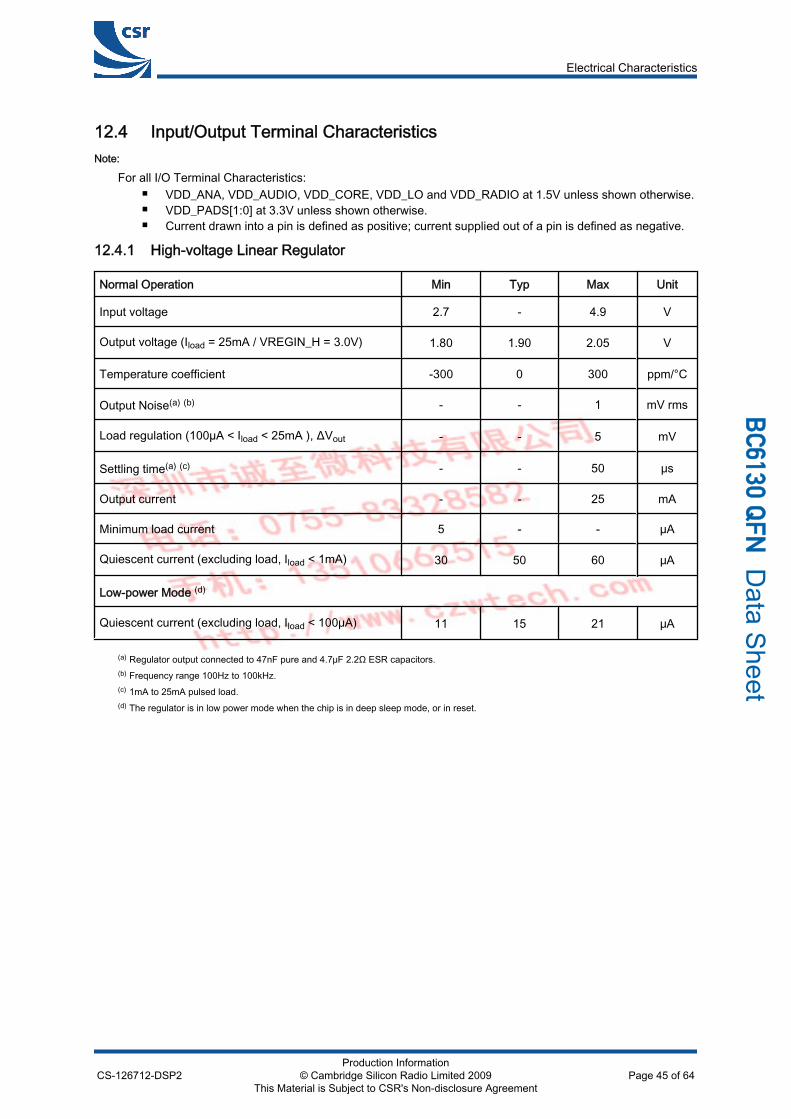
12.4 Input/Output Terminal CharacteristicsNote:
For all I/O Terminal Characteristics: VDD_ANA, VDD_AUDIO, VDD_CORE, VDD_LO and VDD_RADIO at 1.5V unless shown otherwise. VDD_PADS[1:0] at 3.3V unless shown otherwise. Current drawn into a pin is defined as positive; current supplied out of a pin is defined as negative.
12.4.1 High-voltage Linear Regulator
Normal Operation Min Typ Max Unit
Input voltage 2.7 - 4.9 V
Output voltage (Iload = 25mA / VREGIN_H = 3.0V) 1.80 1.90 2.05 V
Temperature coefficient -300 0 300 ppm/°C
Output Noise(a) (b) - - 1 mV rms
Load regulation (100µA < Iload < 25mA ), ΔVout - - 5 mV
Settling time(a) (c) - - 50 μs
Output current - - 25 mA
Minimum load current 5 - - µA
Quiescent current (excluding load, Iload < 1mA) 30 50 60 μA
Low-power Mode (d)
Quiescent current (excluding load, Iload < 100μA) 11 15 21 μA
(a) Regulator output connected to 47nF pure and 4.7μF 2.2Ω ESR capacitors.(b) Frequency range 100Hz to 100kHz.(c) 1mA to 25mA pulsed load.(d) The regulator is in low power mode when the chip is in deep sleep mode, or in reset.
Electrical Characteristics
CS-126712-DSP2Production Information
© Cambridge Silicon Radio Limited 2009This Material is Subject to CSR's Non-disclosure Agreement
Page 45 of 64
_`SNPM=n
ck Data Sheet
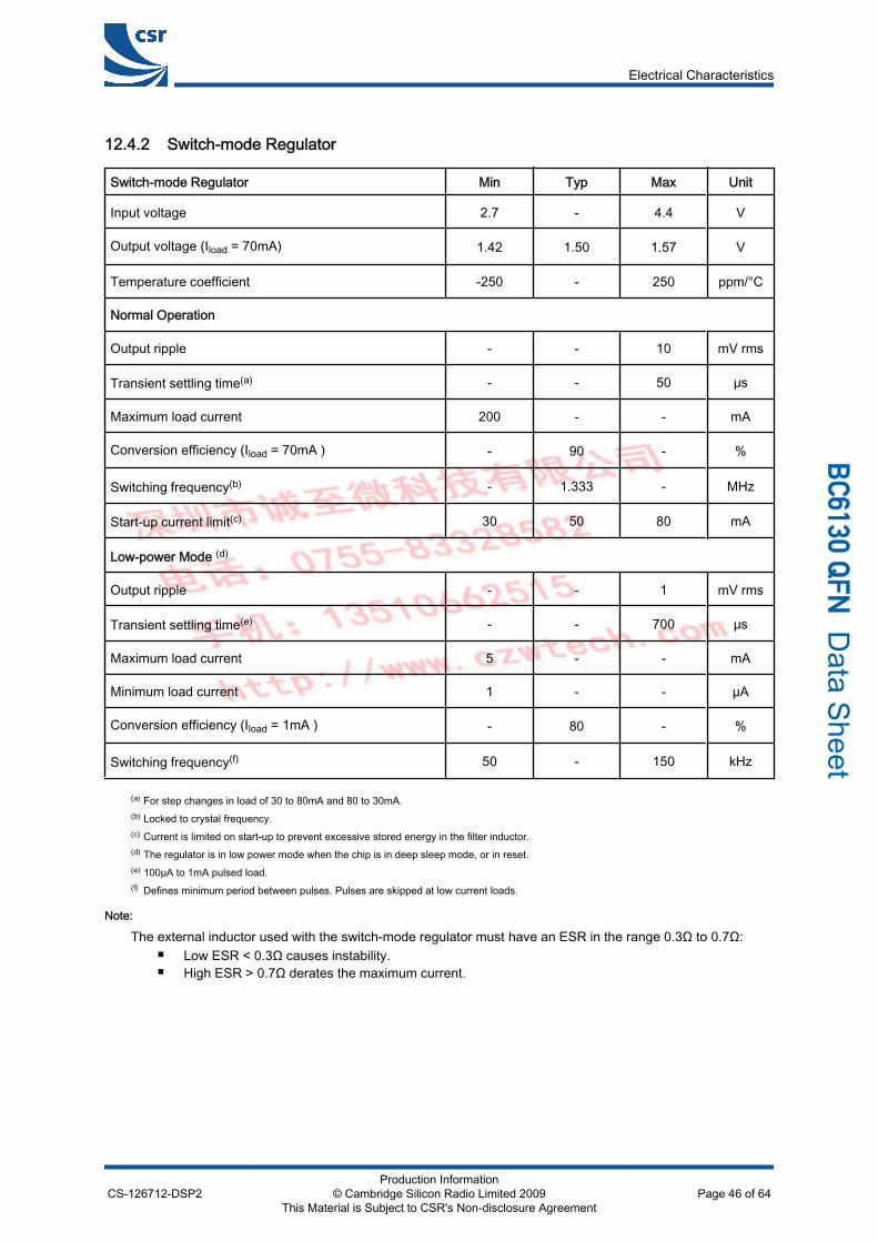
12.4.2 Switch-mode Regulator
Switch-mode Regulator Min Typ Max Unit
Input voltage 2.7 - 4.4 V
Output voltage (Iload = 70mA) 1.42 1.50 1.57 V
Temperature coefficient -250 - 250 ppm/°C
Normal Operation
Output ripple - - 10 mV rms
Transient settling time(a) - - 50 μs
Maximum load current 200 - - mA
Conversion efficiency (Iload = 70mA ) - 90 - %
Switching frequency(b) - 1.333 - MHz
Start-up current limit(c) 30 50 80 mA
Low-power Mode (d)
Output ripple - - 1 mV rms
Transient settling time(e) - - 700 μs
Maximum load current 5 - - mA
Minimum load current 1 - - µA
Conversion efficiency (Iload = 1mA ) - 80 - %
Switching frequency(f) 50 - 150 kHz
(a) For step changes in load of 30 to 80mA and 80 to 30mA.(b) Locked to crystal frequency.(c) Current is limited on start-up to prevent excessive stored energy in the filter inductor.(d) The regulator is in low power mode when the chip is in deep sleep mode, or in reset.(e) 100μA to 1mA pulsed load.(f) Defines minimum period between pulses. Pulses are skipped at low current loads.
Note:
The external inductor used with the switch-mode regulator must have an ESR in the range 0.3Ω to 0.7Ω: Low ESR < 0.3Ω causes instability. High ESR > 0.7Ω derates the maximum current.
Electrical Characteristics
CS-126712-DSP2Production Information
© Cambridge Silicon Radio Limited 2009This Material is Subject to CSR's Non-disclosure Agreement
Page 46 of 64
_`SNPM=n
ck Data Sheet
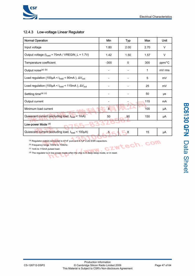
12.4.3 Low-voltage Linear Regulator
Normal Operation Min Typ Max Unit
Input voltage 1.80 2.00 2.70 V
Output voltage (Iload = 70mA / VREGIN_L = 1.7V) 1.42 1.50 1.57 V
Temperature coefficient -300 0 300 ppm/°C
Output noise(a) (b) - - 1 mV rms
Load regulation (100µA < Iload < 90mA ), ΔVout - - 5 mV
Load regulation (100µA < Iload < 115mA ), ΔVout - - 25 mV
Settling time(a) (c) - - 50 μs
Output current - - 115 mA
Minimum load current 5 - 100 µA
Quiescent current (excluding load, Iload < 1mA) 50 90 150 μA
Low-power Mode (d)
Quiescent current (excluding load, Iload < 100μA) 5 8 15 μA
(a) Regulator output connected to 47nF pure and 4.7μF 2.2Ω ESR capacitors.(b) Frequency range 100Hz to 100kHz.(c) 1mA to 115mA pulsed load.(d) The regulator is in low power mode when the chip is in deep sleep mode, or in reset.
Electrical Characteristics
CS-126712-DSP2Production Information
© Cambridge Silicon Radio Limited 2009This Material is Subject to CSR's Non-disclosure Agreement
Page 47 of 64
_`SNPM=n
ck Data Sheet
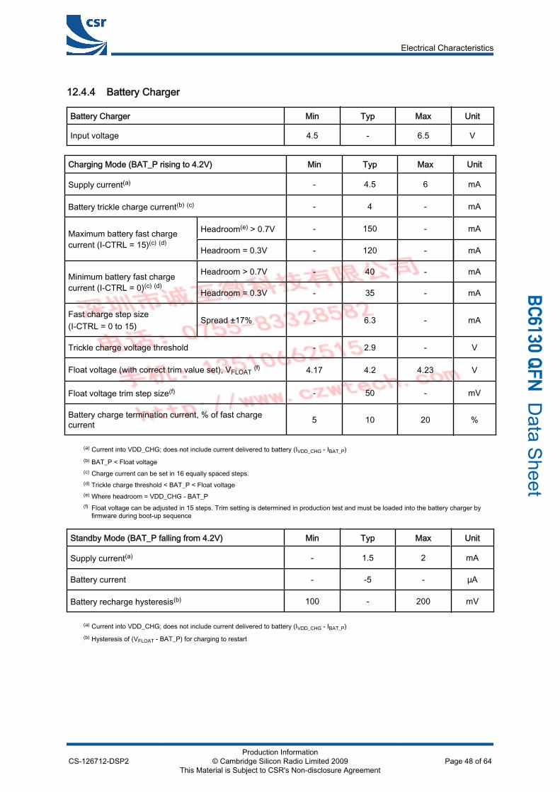
12.4.4 Battery Charger
Battery Charger Min Typ Max Unit
Input voltage 4.5 - 6.5 V
Charging Mode (BAT_P rising to 4.2V) Min Typ Max Unit
Supply current(a) - 4.5 6 mA
Battery trickle charge current(b) (c) - 4 - mA
Maximum battery fast chargecurrent (I-CTRL = 15)(c) (d)
Headroom(e) > 0.7V 150- - mA
mAHeadroom = 0.3V - 120 -
Minimum battery fast chargecurrent (I-CTRL = 0)(c) (d)
mAHeadroom > 0.7V - 40 -
mAHeadroom = 0.3V - 35 -
Fast charge step size(I-CTRL = 0 to 15)
Spread ±17% - 6.3 - mA
Trickle charge voltage threshold - 2.9 - V
Float voltage (with correct trim value set), VFLOAT (f) 4.17 4.2 4.23 V
Float voltage trim step size(f) - 50 - mV
Battery charge termination current, % of fast chargecurrent 5 10 20 %
(a) Current into VDD_CHG; does not include current delivered to battery (IVDD_CHG - IBAT_P)(b) BAT_P < Float voltage(c) Charge current can be set in 16 equally spaced steps.(d) Trickle charge threshold < BAT_P < Float voltage(e) Where headroom = VDD_CHG - BAT_P(f) Float voltage can be adjusted in 15 steps. Trim setting is determined in production test and must be loaded into the battery charger by
firmware during boot-up sequence
Standby Mode (BAT_P falling from 4.2V) Min Typ Max Unit
Supply current(a) - 1.5 2 mA
Battery current - -5 - μA
Battery recharge hysteresis(b) 100 - 200 mV
(a) Current into VDD_CHG; does not include current delivered to battery (IVDD_CHG - IBAT_P)(b) Hysteresis of (VFLOAT - BAT_P) for charging to restart
Electrical Characteristics
CS-126712-DSP2Production Information
© Cambridge Silicon Radio Limited 2009This Material is Subject to CSR's Non-disclosure Agreement
Page 48 of 64
_`SNPM=n
ck Data Sheet
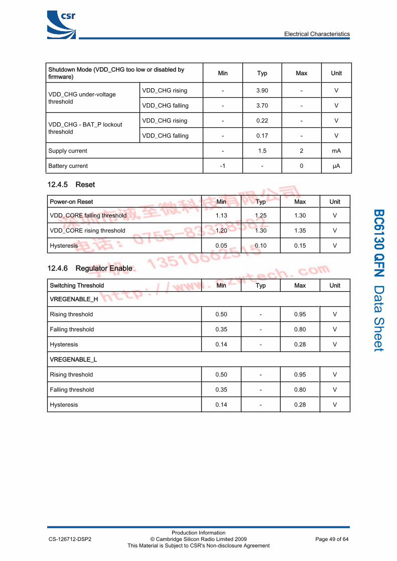
Shutdown Mode (VDD_CHG too low or disabled byfirmware) Min Typ Max Unit
VDD_CHG under-voltagethreshold
VDD_CHG rising - 3.90 - V
VDD_CHG falling - 3.70 - V
VDD_CHG - BAT_P lockoutthreshold
VDD_CHG rising - 0.22 - V
VDD_CHG falling - 0.17 - V
Supply current - 1.5 2 mA
Battery current -1 - 0 μA
12.4.5 Reset
Power-on Reset Min Typ Max Unit
VDD_CORE falling threshold 1.13 1.25 1.30 V
VDD_CORE rising threshold 1.20 1.30 1.35 V
Hysteresis 0.05 0.10 0.15 V
12.4.6 Regulator Enable
Switching Threshold Min Typ Max Unit
VREGENABLE_H
Rising threshold 0.50 - 0.95 V
Falling threshold 0.35 - 0.80 V
Hysteresis 0.14 - 0.28 V
VREGENABLE_L
Rising threshold 0.50 - 0.95 V
Falling threshold 0.35 - 0.80 V
Hysteresis 0.14 - 0.28 V
Electrical Characteristics
CS-126712-DSP2Production Information
© Cambridge Silicon Radio Limited 2009This Material is Subject to CSR's Non-disclosure Agreement
Page 49 of 64
_`SNPM=n
ck Data Sheet

12.4.7 Digital Terminals
Supply Voltage Levels Min Typ Max Unit
VDDPRE 1.4Pre-driver supply voltage 1.5 1.6 V
VDD I/O supplyvoltage (post-driver)
3.0Full spec. 3.3 3.6 V
1.7Reduced spec. - 3.0 V
Input Voltage Levels Min Typ Max Unit
VIL input logic level low -0.3 - 0.25 x VDD V
VIH input logic level high 0.625 x VDD - VDD + 0.3 V
VSCHMITT Schmitt voltage 0.25 x VDD - 0.625 x VDD V
Output Voltage Levels Min Typ Max Unit
VOL output logic level low, lOL = 4.0mA 0 - 0.125 V
VOH output logic level high, lOH = -4.0mA 0.75 x VDD - VDD V
Input and Tristate Currents Min Typ Max Unit
Ii input leakage current at Vin = VDD or 0V -100 0 100 nA
Ioz tristate output leakage current at Vo = VDD or 0V -100 0 100 nA
With strong pull-up -100 -40 -10 μA
With strong pull-down 10 40 100 μA
With weak pull-up -5 -1.0 -0.2 μA
With weak pull-down -0.2 1.0 5.0 μA
CI input capacitance 1.0 - 5.0 pF
Resistive Strength Min Typ Max Unit
Rpuw weak pull-up strength at VDD - 0.2V 0.5 - 2 MΩ
Rpdw weak pull-down strength at 0.2V 0.5 - 2 MΩ
Rpus strong pull-up strength at VDD - 0.2V 10 - 50 kΩ
Rpds strong pull-down strength at 0.2V 10 - 50 kΩ
Electrical Characteristics
CS-126712-DSP2Production Information
© Cambridge Silicon Radio Limited 2009This Material is Subject to CSR's Non-disclosure Agreement
Page 50 of 64
_`SNPM=n
ck Data Sheet
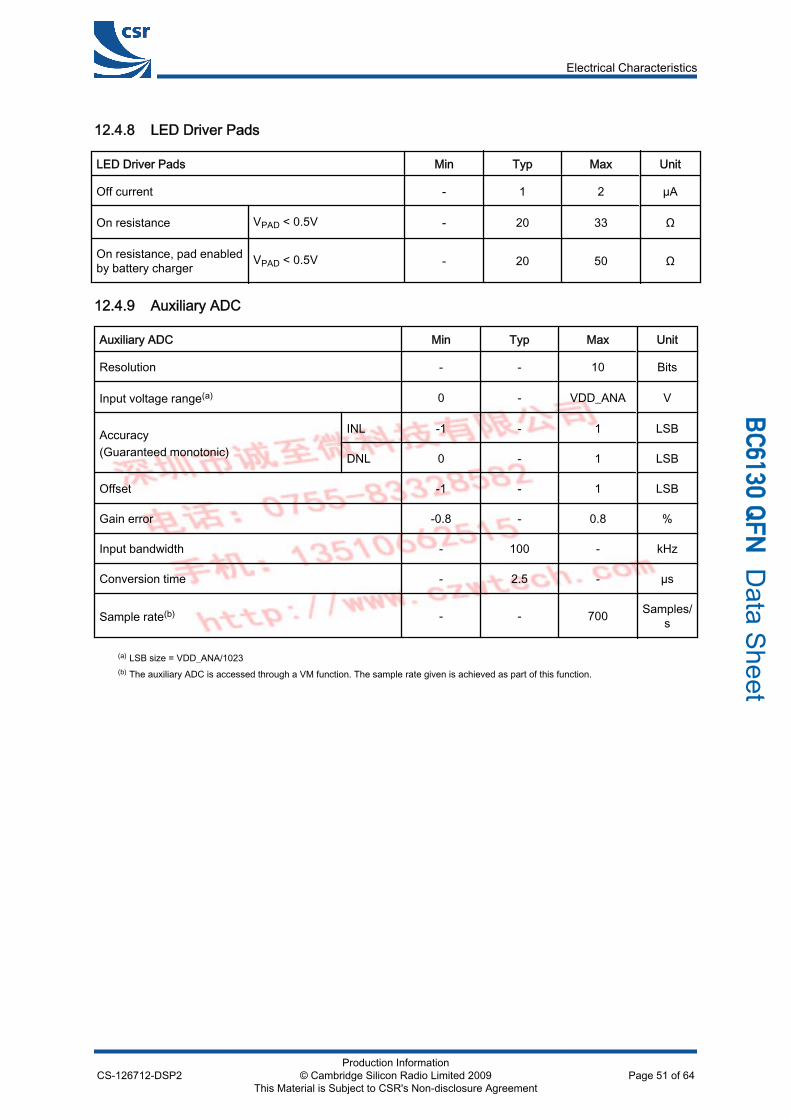
12.4.8 LED Driver Pads
LED Driver Pads Min Typ Max Unit
Off current - 1 2 µA
On resistance VPAD < 0.5V - 20 33 Ω
On resistance, pad enabledby battery charger VPAD < 0.5V - 20 50 Ω
12.4.9 Auxiliary ADC
Auxiliary ADC Min Typ Max Unit
Resolution - - 10 Bits
Input voltage range(a) 0 - VDD_ANA V
Accuracy(Guaranteed monotonic)
INL -1 - 1 LSB
DNL 0 - 1 LSB
Offset -1 - 1 LSB
Gain error -0.8 - 0.8 %
Input bandwidth - 100 - kHz
Conversion time - 2.5 - µs
Sample rate(b) - - 700 Samples/s
(a) LSB size = VDD_ANA/1023(b) The auxiliary ADC is accessed through a VM function. The sample rate given is achieved as part of this function.
Electrical Characteristics
CS-126712-DSP2Production Information
© Cambridge Silicon Radio Limited 2009This Material is Subject to CSR's Non-disclosure Agreement
Page 51 of 64
_`SNPM=n
ck Data Sheet
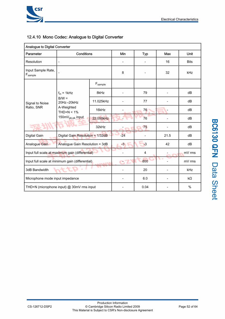
12.4.10 Mono Codec: Analogue to Digital Converter
Analogue to Digital Converter
Parameter Conditions Min Typ Max Unit
Resolution - - - 16 Bits
Input Sample Rate,Fsample
- 8 - 32 kHz
Signal to NoiseRatio, SNR
fin = 1kHzB/W =20Hz→20kHzA-WeightedTHD+N < 1%150mVpk-pk input
Fsample
-8kHz 79 - dB
dB11.025kHz - 77 -
dB16kHz - 76 -
dB22.050kHz - 76 -
dB32kHz - 75 -
Digital Gain Digital Gain Resolution = 1/32dB dB-24 - 21.5
Analogue Gain Analogue Gain Resolution = 3dB dB-3 -3 42
Input full scale at maximum gain (differential) - 4 - mV rms
Input full scale at minimum gain (differential) mV rms- 800 -
3dB Bandwidth kHz- 20 -
Microphone mode input impedance kΩ- 6.0 -
THD+N (microphone input) @ 30mV rms input %- 0.04 -
Electrical Characteristics
CS-126712-DSP2Production Information
© Cambridge Silicon Radio Limited 2009This Material is Subject to CSR's Non-disclosure Agreement
Page 52 of 64
_`SNPM=n
ck Data Sheet
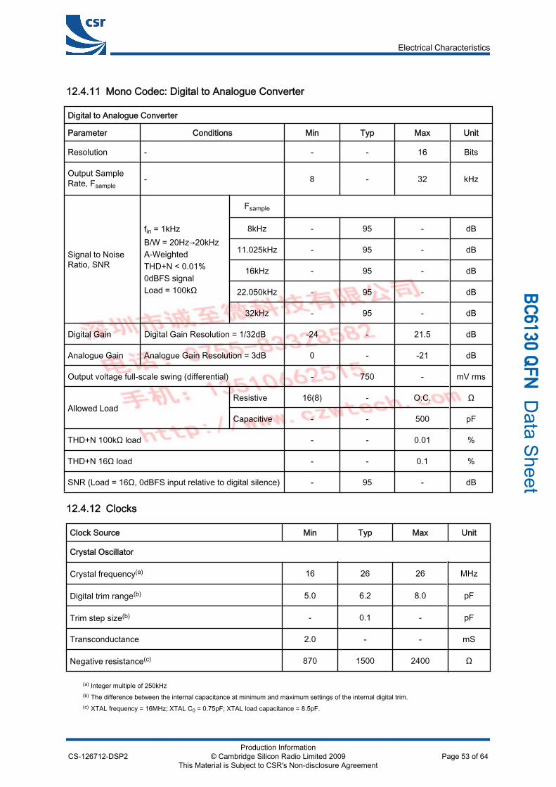
12.4.11 Mono Codec: Digital to Analogue Converter
Digital to Analogue Converter
Parameter Conditions Min Typ Max Unit
Resolution - - - 16 Bits
Output SampleRate, Fsample
- 8 - 32 kHz
Signal to NoiseRatio, SNR
fin = 1kHzB/W = 20Hz→20kHzA-WeightedTHD+N < 0.01%0dBFS signalLoad = 100kΩ
Fsample
8kHz - 95 - dB
11.025kHz - 95 - dB
16kHz - 95 - dB
22.050kHz - 95 - dB
32kHz - 95 - dB
Digital Gain Digital Gain Resolution = 1/32dB -24 - 21.5 dB
Analogue Gain Analogue Gain Resolution = 3dB 0 - -21 dB
Output voltage full-scale swing (differential) - 750 - mV rms
Allowed LoadResistive 16(8) - O.C. Ω
Capacitive - - 500 pF
THD+N 100kΩ load - - 0.01 %
THD+N 16Ω load - - 0.1 %
SNR (Load = 16Ω, 0dBFS input relative to digital silence) - 95 - dB
12.4.12 Clocks
Clock Source Min Typ Max Unit
Crystal Oscillator
Crystal frequency(a) 16 26 26 MHz
Digital trim range(b) 5.0 6.2 8.0 pF
Trim step size(b) - 0.1 - pF
Transconductance 2.0 - - mS
Negative resistance(c) 870 1500 2400 Ω
(a) Integer multiple of 250kHz(b) The difference between the internal capacitance at minimum and maximum settings of the internal digital trim.(c) XTAL frequency = 16MHz; XTAL C0 = 0.75pF; XTAL load capacitance = 8.5pF.
Electrical Characteristics
CS-126712-DSP2Production Information
© Cambridge Silicon Radio Limited 2009This Material is Subject to CSR's Non-disclosure Agreement
Page 53 of 64
_`SNPM=n
ck Data Sheet
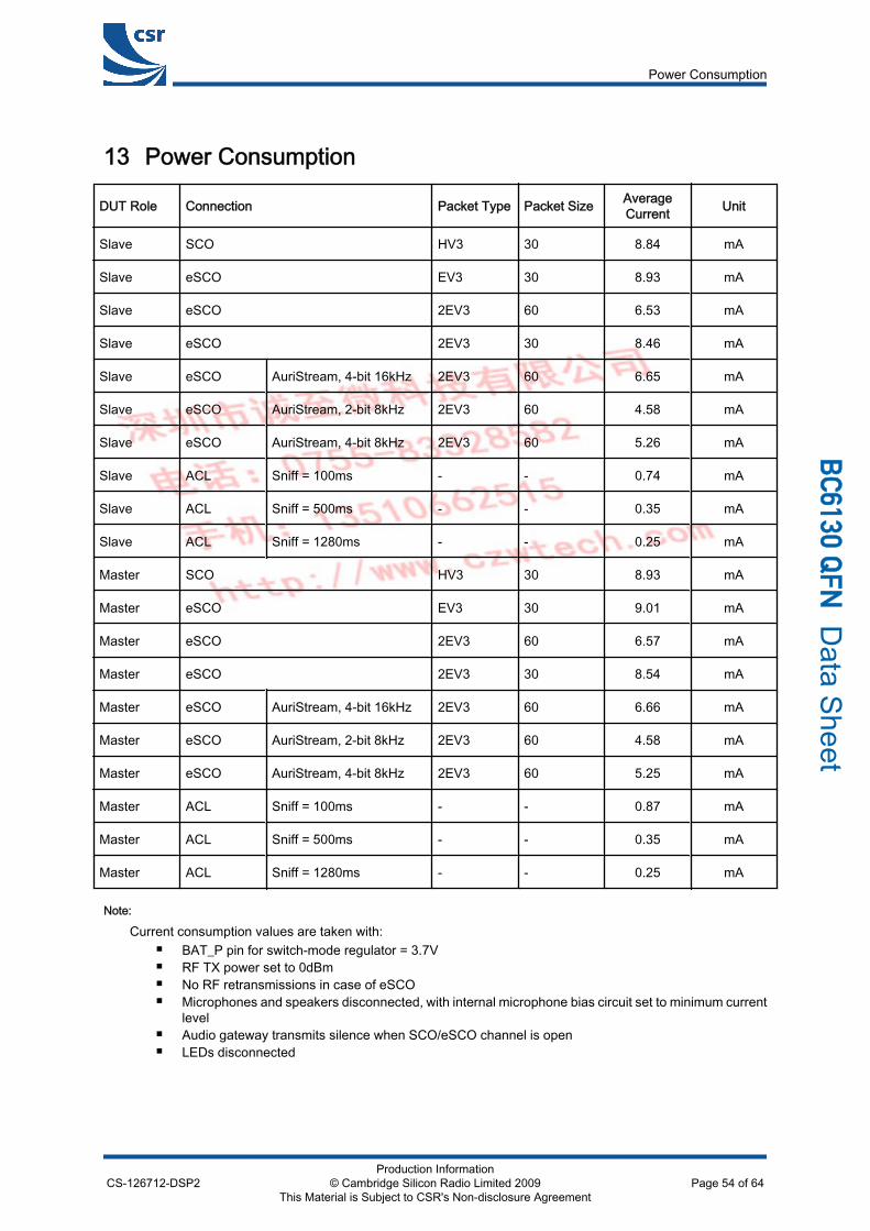
13 Power Consumption
DUT Role Connection Packet Type Packet Size AverageCurrent Unit
Slave SCO HV3 30 8.84 mA
Slave eSCO EV3 30 8.93 mA
Slave eSCO 2EV3 60 6.53 mA
Slave eSCO 2EV3 30 8.46 mA
Slave eSCO AuriStream, 4-bit 16kHz 2EV3 60 6.65 mA
Slave eSCO AuriStream, 2-bit 8kHz 2EV3 60 4.58 mA
Slave eSCO AuriStream, 4-bit 8kHz 2EV3 60 5.26 mA
Slave ACL Sniff = 100ms - - 0.74 mA
Slave ACL Sniff = 500ms - - 0.35 mA
Slave ACL Sniff = 1280ms - - 0.25 mA
Master SCO HV3 30 8.93 mA
Master eSCO EV3 30 9.01 mA
Master eSCO 2EV3 60 6.57 mA
Master eSCO 2EV3 30 8.54 mA
Master eSCO AuriStream, 4-bit 16kHz 2EV3 60 6.66 mA
Master eSCO AuriStream, 2-bit 8kHz 2EV3 60 4.58 mA
Master eSCO AuriStream, 4-bit 8kHz 2EV3 60 5.25 mA
Master ACL Sniff = 100ms - - 0.87 mA
Master ACL Sniff = 500ms - - 0.35 mA
Master ACL Sniff = 1280ms - - 0.25 mA
Note:
Current consumption values are taken with: BAT_P pin for switch-mode regulator = 3.7V RF TX power set to 0dBm No RF retransmissions in case of eSCO Microphones and speakers disconnected, with internal microphone bias circuit set to minimum current
level Audio gateway transmits silence when SCO/eSCO channel is open LEDs disconnected
Power Consumption
CS-126712-DSP2Production Information
© Cambridge Silicon Radio Limited 2009This Material is Subject to CSR's Non-disclosure Agreement
Page 54 of 64
_`SNPM=n
ck Data Sheet
14 CSR Green Semiconductor Products and RoHS Compliance14.1 RoHS StatementBC6130 QFN where explicitly stated in this Data Sheet meets the requirements of Directive 2002/95/EC of theEuropean Parliament and of the Council on the Restriction of Hazardous Substance (RoHS).
14.1.1 List of Restricted MaterialsBC6130 QFN is compliant with RoHS in relation to the following substances:
Cadmium Lead Mercury Hexavalent chromium Polybrominated Biphenyl Polybrominated Diphenyl Ether
In addition, the following substances are not intentionally added to BC6130 QFN devices:
Halogenated flame retardant Antimony (Sb) and Compounds, including Antimony Trioxide flame retardant Polybrominated Diphenyl and Biphenyl Oxides Tetrabromobisphenol-A bis (2,3-dibromopropylether) Asbestos or Asbestos compounds Azo compounds Organic tin compounds Mirex Polychlorinated napthelenes Polychlorinated terphenyls Polychlorinated biphenyls Polychlorinated/Short chain chlorinated paraffins Polyvinyl Chloride (PVC) and PVC blends Formaldehyde Arsenic and compounds (except as a semiconductor dopant) Beryllium and its compounds Ethylene Glycol Monomethyl Ether or its acetate Ethylene Glycol Monoethyl Ether or its acetate Halogenated dioxins and furans Persistent Organic Pollutants (POP), including Perfluorooctane sulphonates Red phosphorous Ozone Depleting Chemicals (Class I and II): Chlorofluorocarbons (CFC) and Halons Radioactive substances
For further information, see CSR's Environmental Compliance Statement for CSR Green Semiconductor Products.
CSR Green Semiconductor Products and RoHS Compliance
CS-126712-DSP2Production Information
© Cambridge Silicon Radio Limited 2009This Material is Subject to CSR's Non-disclosure Agreement
Page 55 of 64
_`SNPM=n
ck Data Sheet
15 CSR Bluetooth Software StackBC6130 QFN is supplied with Bluetooth v2.1 + EDR specification compliant stack firmware, which runs on the internalRISC MCU.
The BC6130 QFN software architecture allows Bluetooth processing and the application program to be run on theinternal RISC MCU. The upper layers of the Bluetooth stack, above the HCI, are run on-chip.
15.1 BC6130 Low-cost Mono Headset Solution Development KitCSR’s BC6130 low-cost mono headset solution development kit for BC6130 QFN, order code DK-BC-6130-1A,includes a headset demonstrator board, form-factor representative example design, music and voice dongle andnecessary interface adapters and cables. In conjunction with the BlueVox Configurator tool and other supportingutilities the development kit provides the best environment for designing a mono headset solution with BC6130 QFN.
15.2 BC6130 Low-cost Mono Headset Solution Software (BC6130A04) The CSR mono headset ROM software supports HFP v1.5 and HSP v1.1. Advanced features in these
specifications are supported, including three-way calling. Bluetooth v2.1 + EDR specification is supported in the ROM software including Secure Simple Pairing,
greatly simplifying the pairing process. Proximity Pairing (headset initiated pairing) for greatly simplifying the out-of-box pairing process, for more
information see Section 15.5. For connection to more than one mobile phone Advanced Multipoint is supported. This allows a user to
take calls from a work and personal phone or a work phone and a VoIP dongle for Skype users. This issupported with a minimal impact on power consumption and can be easily configured.
The BC6130 low-cost mono headset solution includes noise reduction hardware controlled by the on-chipMCU. This improves the clarity of the speech in noisy environments.
Most of the CSR mono headset ROM software features can be configured on the BC6130 QFN using theBlueVox Configurator tool available from www.csrsupport.com/MonoHeadsetSolutions . The tool can beused to read and write headset configurations directly to the EEPROM or alternatively to a PSR file.Configurable headset features include: Bluetooth v2.1 + EDR specification features Reconnection policies, e.g. reconnect on power on Audio features, including default volumes Button events: configuring button presses and durations for certain events, e.g. double press on
PIO[1] for Last Number redial LED indications for states, e.g. headset connected, and events, e.g. power on Indication tones for events and ringtones HFP v1.5 supported features Battery divider ratios and thresholds, e.g. thresholds for battery low indication, full battery etc. Advanced Multipoint settings
The BC6130 low-cost mono headset solution includes the AuriStream, CSR's proprietary ADPCM codecwhich can be configured for low power consumption or improved audio quality
The BC6130 low-cost mono headset solution has undergone extensive interoperability testing to ensurethat it works with the majority of phones on the market
15.3 Advanced Multipoint SupportAdvanced Multipoint allows the connection of 2 devices to BC6130 QFN at the same time. For example, this couldbe either 2 phones connected to a BC6130 QFN headset, or a phone and a VoIP dongle connected to a headset.
The BC6130 low-cost mono headset solution: Supports a maximum of 2 connections (either HFP or HSP) Allows multiple calls to be handled from both devices at the same time During a call from 1 device, all headset buttons work as in the standard use case with one device connected During multiple calls (1 on each device), all headset buttons work as in the standard use case for a single
AG with multiple calls in progress (three-way calling) This implementation is easy to use with negligible effect on power consumption
CSR Bluetooth Software Stack
CS-126712-DSP2Production Information
© Cambridge Silicon Radio Limited 2009This Material is Subject to CSR's Non-disclosure Agreement
Page 56 of 64
_`SNPM=n
ck Data Sheet
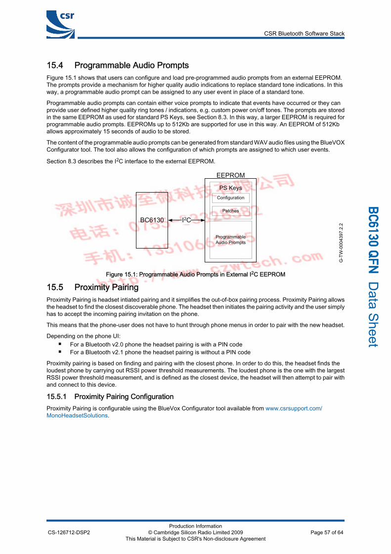
15.4 Programmable Audio PromptsFigure 15.1 shows that users can configure and load pre-programmed audio prompts from an external EEPROM.The prompts provide a mechanism for higher quality audio indications to replace standard tone indications. In thisway, a programmable audio prompt can be assigned to any user event in place of a standard tone.
Programmable audio prompts can contain either voice prompts to indicate that events have occurred or they canprovide user defined higher quality ring tones / indications, e.g. custom power on/off tones. The prompts are storedin the same EEPROM as used for standard PS Keys, see Section 8.3. In this way, a larger EEPROM is required forprogrammable audio prompts. EEPROMs up to 512Kb are supported for use in this way. An EEPROM of 512Kballows approximately 15 seconds of audio to be stored.
The content of the programmable audio prompts can be generated from standard WAV audio files using the BlueVOXConfigurator tool. The tool also allows the configuration of which prompts are assigned to which user events.
Section 8.3 describes the I2C interface to the external EEPROM.
G-T
W-0
0043
97.2
.2
BC6130
EEPROM
I2C
PS Keys
Programmable Audio Prompts
Patches
Configuration
Figure 15.1: Programmable Audio Prompts in External I2C EEPROM
15.5 Proximity PairingProximity Pairing is headset intiated pairing and it simplifies the out-of-box pairing process. Proximity Pairing allowsthe headset to find the closest discoverable phone. The headset then initiates the pairing activity and the user simplyhas to accept the incoming pairing invitation on the phone.
This means that the phone-user does not have to hunt through phone menus in order to pair with the new headset.
Depending on the phone UI: For a Bluetooth v2.0 phone the headset pairing is with a PIN code For a Bluetooth v2.1 phone the headset pairing is without a PIN code
Proximity pairing is based on finding and pairing with the closest phone. In order to do this, the headset finds theloudest phone by carrying out RSSI power threshold measurements. The loudest phone is the one with the largestRSSI power threshold measurement, and is defined as the closest device, the headset will then attempt to pair withand connect to this device.
15.5.1 Proximity Pairing ConfigurationProximity Pairing is configurable using the BlueVox Configurator tool available from www.csrsupport.com/MonoHeadsetSolutions.
CSR Bluetooth Software Stack
CS-126712-DSP2Production Information
© Cambridge Silicon Radio Limited 2009This Material is Subject to CSR's Non-disclosure Agreement
Page 57 of 64
_`SNPM=n
ck Data Sheet
16 Ordering Information
DevicePackage
Order NumberType Size Shipment
Method
BC6130 Low-costMono HeadsetSolution
QFN 48-lead(Pb free)
7 x 7 x 0.9mm,0.5mm pitch
Tape and reel BC6130A04-IQQB-R
Note:
BC6130 QFN is a ROM-based device where the product code has the form BC6130Axx. Axx is the specificROM-variant, A04 is the ROM-variant for BC6130 Low-cost Mono Headset Solution.
Minimum order quantity is 2kpcs taped and reeled.
Supply chain: CSR's manufacturing policy is to multisource volume products. For further details, contact yourlocal sales account manager or representative.
To contact a CSR representative, email [email protected] or go to www.csr.com/contacts.
16.1 BC6130 Low-cost Mono Headset Solution Development Kit OrderingInformation
Description Order Number
BC6130 Low-cost Mono Headset Solution Development Kit, includingheadset example design DK-BC-6130-1A
Ordering Information
CS-126712-DSP2Production Information
© Cambridge Silicon Radio Limited 2009This Material is Subject to CSR's Non-disclosure Agreement
Page 58 of 64
_`SNPM=n
ck Data Sheet
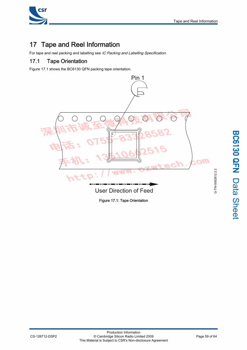
17 Tape and Reel InformationFor tape and reel packing and labelling see IC Packing and Labelling Specification.
17.1 Tape OrientationFigure 17.1 shows the BC6130 QFN packing tape orientation.
G-T
W-0
0028
12.2
.2
User Direction of Feed
Pin 1
Figure 17.1: Tape Orientation
Tape and Reel Information
CS-126712-DSP2Production Information
© Cambridge Silicon Radio Limited 2009This Material is Subject to CSR's Non-disclosure Agreement
Page 59 of 64
_`SNPM=n
ck Data Sheet
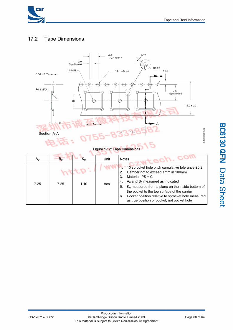
17.2 Tape Dimensions
G-T
W-0
0028
11.3
.2
4.0See Note 1
12.0
0.25
R0.25
Bo
AoKo
1.75
2.0See Note 6
0.30 ± 0.05 A
A
Section A-A
7.5See Note 6
R0.3 MAX
±
Figure 17.2: Tape Dimensions
A0 B0 K0 Unit Notes
7.25 7.25 1.10 mm
1. 10 sprocket hole pitch cumulative tolerance ±0.22. Camber not to exceed 1mm in 100mm3. Material: PS + C4. A0 and B0 measured as indicated5. K0 measured from a plane on the inside bottom of
the pocket to the top surface of the carrier6. Pocket position relative to sprocket hole measured
as true position of pocket, not pocket hole
Tape and Reel Information
CS-126712-DSP2Production Information
© Cambridge Silicon Radio Limited 2009This Material is Subject to CSR's Non-disclosure Agreement
Page 60 of 64
_`SNPM=n
ck Data Sheet
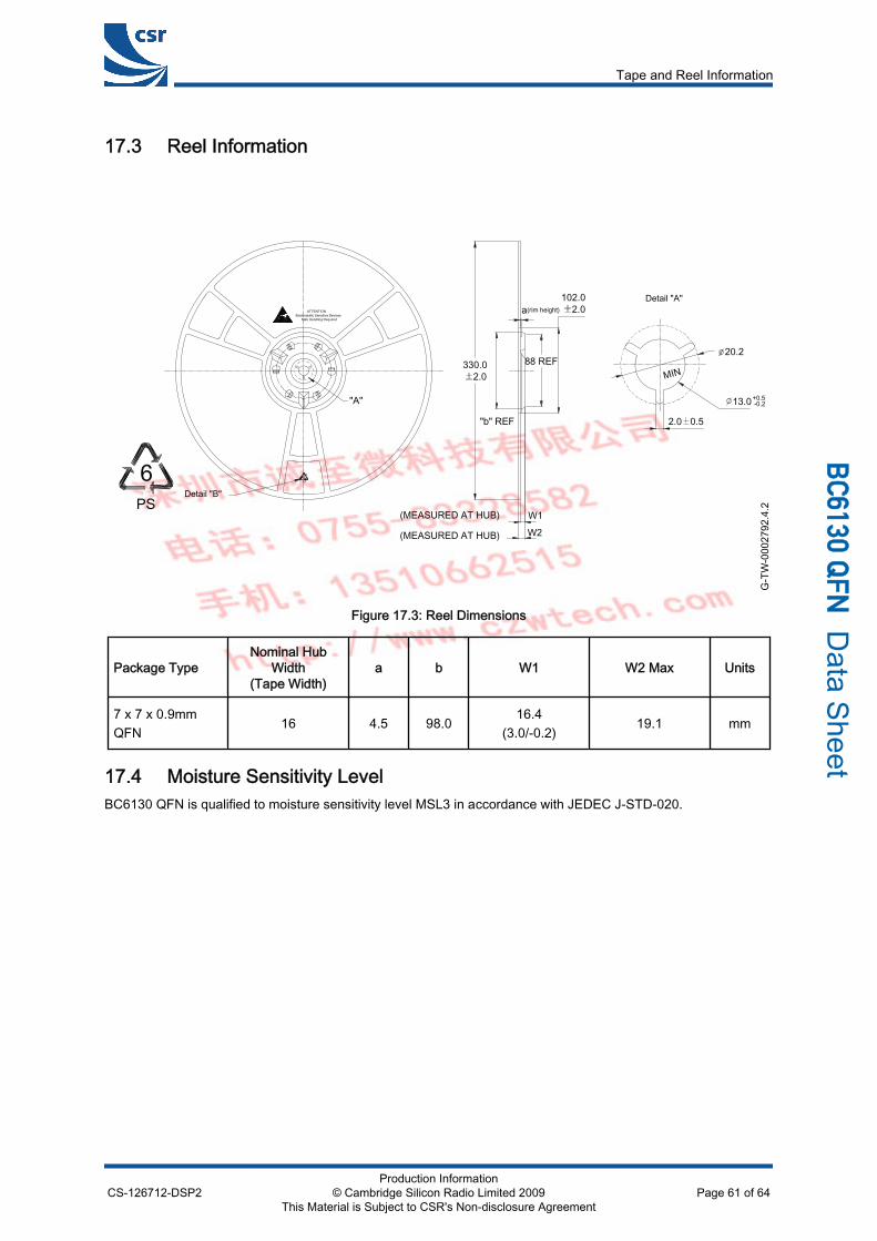
17.3 Reel Information
G-T
W-0
0027
92.4
.2
102.02.0
330.02.0
W1(MEASURED AT HUB)
(MEASURED AT HUB)
"A"
ATTENTIONElectrostatic Sensitive Devices Safe Handling Required
W2
20.2
MIN
2.0 0.5
13.0+0.5-0.2
Detail "A"
Detail "B"
6 PS
PS
6
a(rim height)
88 REF
"b" REF
Figure 17.3: Reel Dimensions
Package TypeNominal Hub
Width(Tape Width)
a b W1 W2 Max Units
7 x 7 x 0.9mmQFN
16 4.5 98.016.4
(3.0/-0.2)19.1 mm
17.4 Moisture Sensitivity LevelBC6130 QFN is qualified to moisture sensitivity level MSL3 in accordance with JEDEC J-STD-020.
Tape and Reel Information
CS-126712-DSP2Production Information
© Cambridge Silicon Radio Limited 2009This Material is Subject to CSR's Non-disclosure Agreement
Page 61 of 64
_`SNPM=n
ck Data Sheet
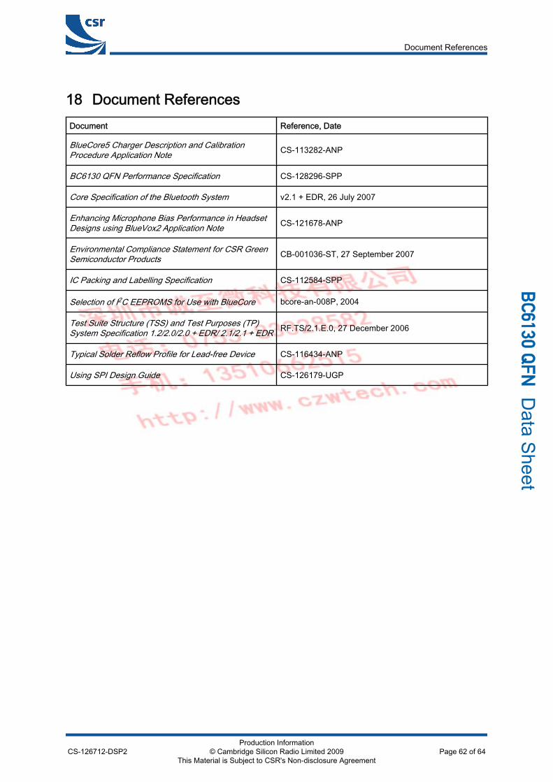
18 Document ReferencesDocument Reference, Date
BlueCore5 Charger Description and CalibrationProcedure Application Note CS-113282-ANP
BC6130 QFN Performance Specification CS-128296-SPP
Core Specification of the Bluetooth System v2.1 + EDR, 26 July 2007
Enhancing Microphone Bias Performance in HeadsetDesigns using BlueVox2 Application Note CS-121678-ANP
Environmental Compliance Statement for CSR GreenSemiconductor Products CB-001036-ST, 27 September 2007
IC Packing and Labelling Specification CS-112584-SPP
Selection of I2C EEPROMS for Use with BlueCore bcore-an-008P, 2004
Test Suite Structure (TSS) and Test Purposes (TP)System Specification 1.2/2.0/2.0 + EDR/ 2.1/2.1 + EDR RF.TS/2.1.E.0, 27 December 2006
Typical Solder Reflow Profile for Lead-free Device CS-116434-ANP
Using SPI Design Guide CS-126179-UGP
Document References
CS-126712-DSP2Production Information
© Cambridge Silicon Radio Limited 2009This Material is Subject to CSR's Non-disclosure Agreement
Page 62 of 64
_`SNPM=n
ck Data Sheet
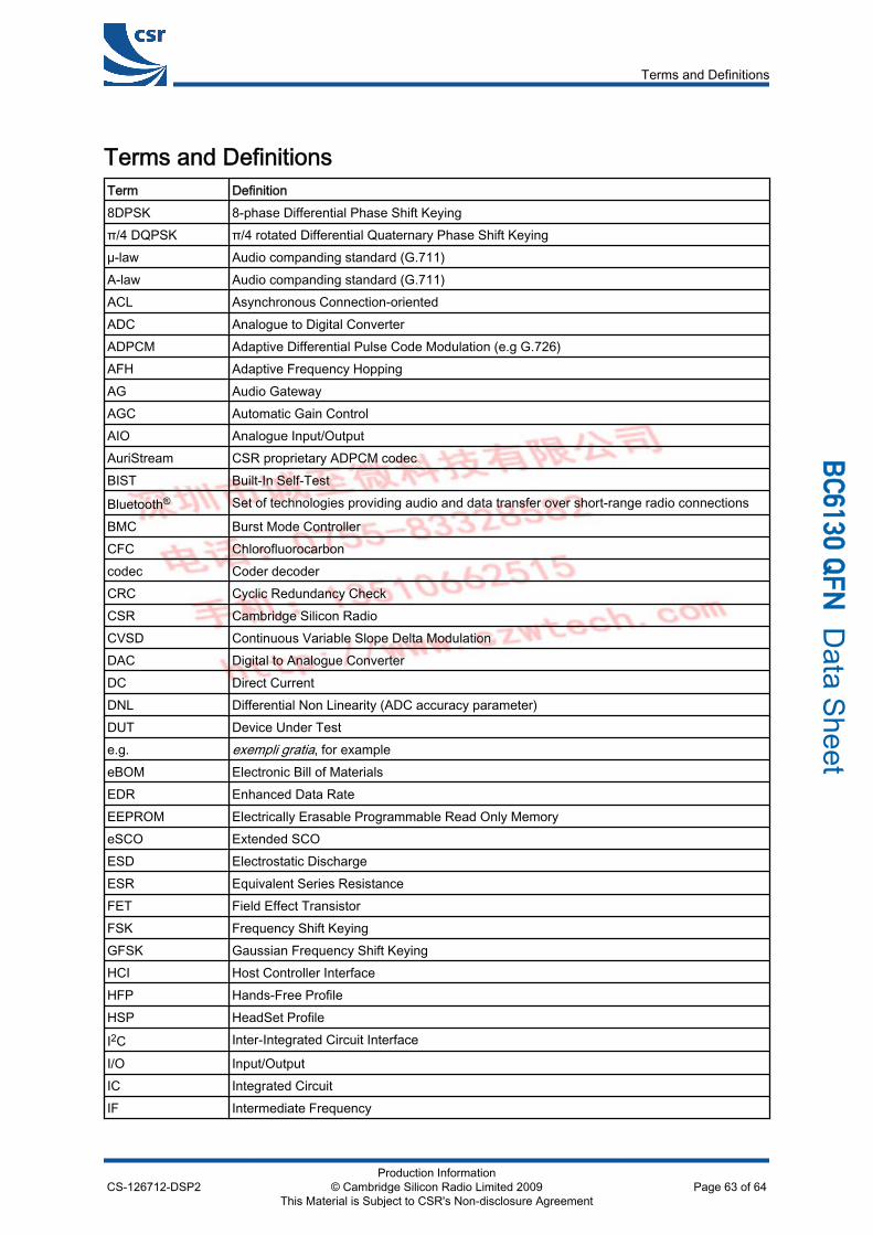
Terms and DefinitionsTerm Definition8DPSK 8-phase Differential Phase Shift Keyingπ/4 DQPSK π/4 rotated Differential Quaternary Phase Shift Keyingµ-law Audio companding standard (G.711)A-law Audio companding standard (G.711)ACL Asynchronous Connection-orientedADC Analogue to Digital ConverterADPCM Adaptive Differential Pulse Code Modulation (e.g G.726)AFH Adaptive Frequency HoppingAG Audio GatewayAGC Automatic Gain ControlAIO Analogue Input/OutputAuriStream CSR proprietary ADPCM codecBIST Built-In Self-Test
Bluetooth® Set of technologies providing audio and data transfer over short-range radio connections
BMC Burst Mode ControllerCFC Chlorofluorocarboncodec Coder decoderCRC Cyclic Redundancy CheckCSR Cambridge Silicon RadioCVSD Continuous Variable Slope Delta ModulationDAC Digital to Analogue ConverterDC Direct CurrentDNL Differential Non Linearity (ADC accuracy parameter)DUT Device Under Teste.g. exempli gratia, for exampleeBOM Electronic Bill of MaterialsEDR Enhanced Data RateEEPROM Electrically Erasable Programmable Read Only MemoryeSCO Extended SCOESD Electrostatic DischargeESR Equivalent Series ResistanceFET Field Effect TransistorFSK Frequency Shift KeyingGFSK Gaussian Frequency Shift KeyingHCI Host Controller InterfaceHFP Hands-Free ProfileHSP HeadSet Profile
I2C Inter-Integrated Circuit Interface
I/O Input/OutputIC Integrated CircuitIF Intermediate Frequency
Terms and Definitions
CS-126712-DSP2Production Information
© Cambridge Silicon Radio Limited 2009This Material is Subject to CSR's Non-disclosure Agreement
Page 63 of 64
_`SNPM=n
ck Data Sheet
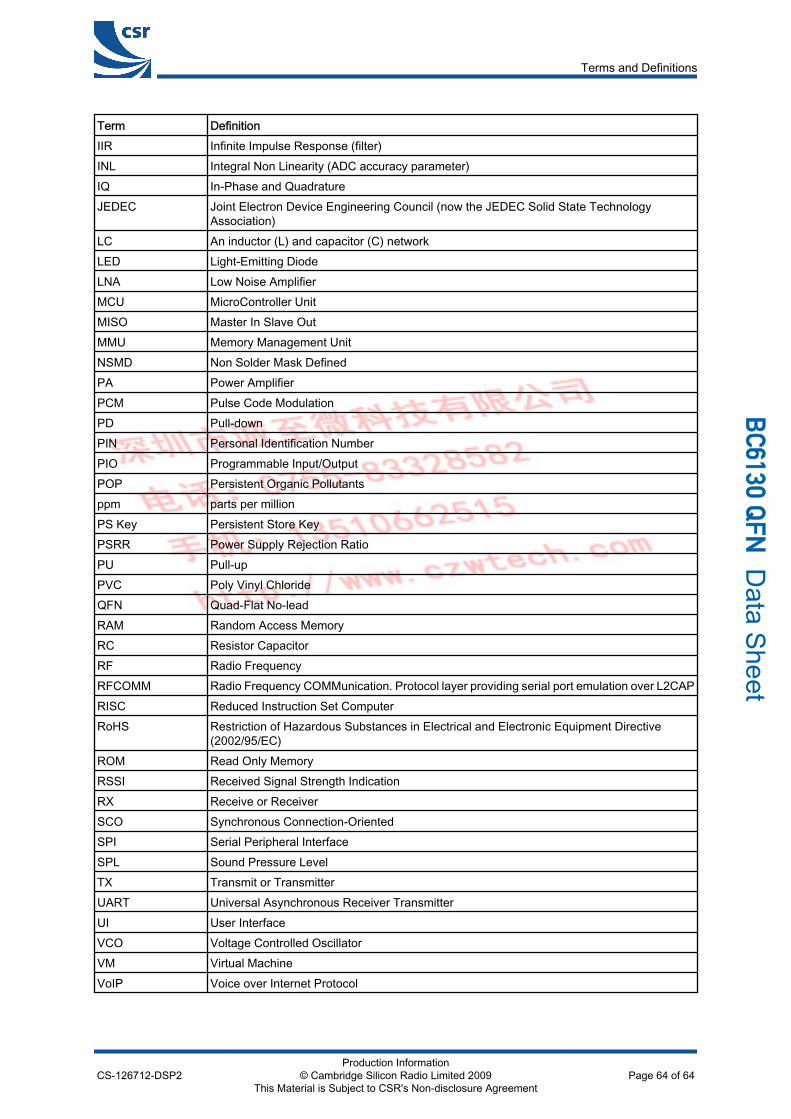
Term DefinitionIIR Infinite Impulse Response (filter)INL Integral Non Linearity (ADC accuracy parameter)IQ In-Phase and QuadratureJEDEC Joint Electron Device Engineering Council (now the JEDEC Solid State Technology
Association)LC An inductor (L) and capacitor (C) networkLED Light-Emitting DiodeLNA Low Noise AmplifierMCU MicroController UnitMISO Master In Slave OutMMU Memory Management UnitNSMD Non Solder Mask DefinedPA Power AmplifierPCM Pulse Code ModulationPD Pull-downPIN Personal Identification NumberPIO Programmable Input/OutputPOP Persistent Organic Pollutantsppm parts per millionPS Key Persistent Store KeyPSRR Power Supply Rejection RatioPU Pull-upPVC Poly Vinyl ChlorideQFN Quad-Flat No-leadRAM Random Access MemoryRC Resistor CapacitorRF Radio FrequencyRFCOMM Radio Frequency COMMunication. Protocol layer providing serial port emulation over L2CAPRISC Reduced Instruction Set ComputerRoHS Restriction of Hazardous Substances in Electrical and Electronic Equipment Directive
(2002/95/EC)ROM Read Only MemoryRSSI Received Signal Strength IndicationRX Receive or ReceiverSCO Synchronous Connection-OrientedSPI Serial Peripheral InterfaceSPL Sound Pressure LevelTX Transmit or TransmitterUART Universal Asynchronous Receiver TransmitterUI User InterfaceVCO Voltage Controlled OscillatorVM Virtual MachineVoIP Voice over Internet Protocol
Terms and Definitions
CS-126712-DSP2Production Information
© Cambridge Silicon Radio Limited 2009This Material is Subject to CSR's Non-disclosure Agreement
Page 64 of 64
_`SNPM=n
ck Data Sheet