Embed Size (px)
Citation preview

Software-Based Online Detection of Hardware Defects:Mechanisms, Architectural Support, and Evaluation
Kypros Constantinides‡ Onur Mutlu† Todd Austin‡ Valeria Bertacco‡
‡Advanced Computer Architecture Lab †Computer Architecture GroupUniversity of Michigan Microsoft Research
Ann Arbor, MI Redmond, WA{kypros, austin, valeria}@umich.edu [email protected]
AbstractAs silicon process technology scales deeper into the nanometerregime, hardware defects are becoming more common. Such de-fects are bound to hinder the correct operation of future processorsystems, unless new online techniques become available to detectand to tolerate them while preserving the integrity of softwareapplications running on the system.
This paper proposes a new, software-based, defect detectionand diagnosis technique. We introduce a novel set of instruc-tions, called Access-Control Extension (ACE), that can accessand control the microprocessor’s internal state. Special firmwareperiodically suspends microprocessor execution and uses the ACEinstructions to run directed tests on the hardware. When a hard-ware defect is present, these tests can diagnose and locate it,and then activate system repair through resource reconfigura-tion. The software nature of our framework makes it flexible:testing techniques can be modified/upgraded in the field to tradeoff performance with reliability without requiring any change tothe hardware.
We evaluated our technique on a commercial chip-multiprocessorbased on Sun’s Niagara and found that it can provide very highcoverage, with 99.22% of all silicon defects detected. Moreover,our results show that the average performance overhead of software-based testing is only 5.5%. Based on a detailed RTL-level imple-mentation of our technique, we find its area overhead to be quitemodest, with only a 5.8% increase in total chip area.
1. IntroductionThe impressive growth of the semiconductor industry over
the last few decades is fueled by continuous silicon scaling,which offers smaller, faster, and cheaper transistors witheach new technology generation. However, challenges in pro-ducing reliable components in these extremely dense tech-nologies are growing, with many device experts warning thatcontinued scaling will inevitably lead to future generationsof silicon technology being much less reliable than presentones [3, 32]. Processors manufactured in future technologieswill likely experience failures in the field due to silicon de-fects occurring during system operation. In the absence ofany viable alternative technology, the success of the semi-conductor industry in the future will depend on the creationof cost-effective mechanisms to tolerate silicon defects in thefield (i.e., during operation).
The Challenge - Tolerating Hardware Defects: Totolerate permanent hardware faults (i.e., silicon defects) en-countered during operation, a reliable system requires theinclusion of three critical capabilities: 1) mechanisms fordetection and diagnosis of defects, 2) recovery techniques torestore correct system state after a fault is detected, and3) repair mechanisms to restore correct system functional-ity for future computation. Fortunately, research in chip-
multiprocessor (CMP) architectures already provides for thelatter two requirements. Researchers have pursued the de-velopment of global checkpoint and recovery mechanisms,examples of these include SafetyNet [31] and ReVive [22,19]. These low-cost checkpointing mechanisms provide thecapabilities necessary to implement system recovery.
Additionally, the highly redundant nature of future CMPswill allow low-cost repair through the disabling of defectiveprocessing elements [27]. With a sufficient number of pro-cessing resources, the performance of a future parallel sys-tem will gracefully degrade as manifested defects increase.Moreover, the performance impact of each degradation stepis expected to decrease substantially as future CMP systemsscale to larger numbers of processing elements.
Given the existence of low-cost mechanisms for system re-covery and repair, the remaining major challenge in the de-sign of a defect-tolerant CMP is the development of low-costdefect detection techniques. Existing online hardware-baseddefect detection and diagnosis techniques can be classifiedinto two broad categories 1) continuous: those that continu-ously check for execution errors and 2) periodic: those thatperiodically check the processor’s logic.
Existing Defect Tolerance Techniques and theirShortcomings: Examples of continuous techniques are DualModular Redundancy (DMR) [29] and DIVA [2]. Thesetechniques detect silicon defects by validating the executionthrough independent redundant computation. However, in-dependent redundant computation requires significant hard-ware cost in terms of silicon area (100% extra hardware inthe case of DMR). Furthermore, continuous checking con-sumes significant energy and requires part of the maximumpower envelope to be dedicated to it. In contrast, periodic
techniques check periodically the integrity of the hardwarewithout requiring redundant execution [28]. These tech-niques rely on checkpointing and recovery mechanisms thatprovide computational epochs and a substrate for specu-lative unchecked execution. At the end of each computa-tional epoch, the hardware is checked by on-chip testers. Ifthe hardware tests succeed, the results produced during theepoch are committed and execution proceeds to the nextcomputational epoch. Otherwise, the system is deemed de-fective and system repair and recovery are required.
The on-chip testers employed by periodic defect tolerancetechniques rely on the same Built-In-Self-Test (BIST) tech-niques that are used predominantly during manufacturingtesting [6]. BIST techniques use specialized circuitry to gen-erate test patterns and to validate the responses generatedby the hardware. There are two main ways to generate test

patterns on chip: (1) by using pseudo-random test patterngenerators, (2) by storing on-chip previously generated testvectors that are based on a specific fault model. Unfortu-nately, both of these approaches have significant drawbacks.The first approach does not follow any specific testing strat-egy (targeted fault model) and therefore requires extendedtesting times to achieve good fault coverage [6]. The sec-ond approach, not only requires significant hardware over-head [7] to store the test patterns on chip, but also bindsa specific testing approach (i.e., fault model) into silicon.On the other hand, as the nature of wearout-related silicondefects and the techniques to detect them are under con-tinuous exploration [10], binding specific testing approachesinto silicon might be premature and therefore undesirable.
As of today, hardware-based defect tolerance techniqueshave one or both of the following two major disadvantages:
1. Cost: They require significant additional hardware toimplement a specific testing strategy,
2. Inflexibility: They bind specific test patterns and a spe-cific testing approach (e.g., based on a specific fault model)into silicon. Thus, it is impossible to change the testingstrategy and test patterns after the processor is deployedin the field. Flexible defect tolerance solutions that can bemodified, upgraded, and tuned in the field are very desir-able.
Motivation and Basic Idea: Our goal in this paperis to develop a low-cost, flexible defect tolerance techniquethat can be modified and upgraded in the field. To thisend, we propose to implement hardware defect detection and
diagnosis in software. In our approach, the hardware pro-vides the necessary substrate to facilitate testing and thesoftware makes use of this substrate to perform the testing.We introduce specialized Access-Control Extension (ACE)instructions that are capable of accessing and controllingvirtually any portion of the microprocessor’s internal state.Special firmware periodically suspends microprocessor exe-cution and uses the ACE instructions to run directed testson the hardware and detect if any component has becomedefective. To provide faster and more flexible software accessto different microarchitectural components at low hardwareoverhead, our scheme leverages the pre-existing scan-chaininfrastructure [12] that is conventionally integrated in mi-croprocessor designs today and used during manufacturingtesting.
Figure 1 shows how the ACE framework fits in the hard-ware/software stack below the operating system layer. Ourapproach provides particularly wide coverage, as it not onlytests the internal processor control and instruction sequenc-ing mechanisms through software functional testing, but itcan also check all datapaths, routers, interconnect and mi-croarchitectural components by issuing ACE instruction testsequences. We provide a complete defect tolerance solutionby incorporating our defect detection and diagnosis tech-nique in a coarse-grained checkpointing and recovery envi-ronment. If an ACE test sequence detects that the under-lying hardware is defective, the system disables the defec-tive component and restores correct program state by rollingback to the last known correct checkpoint.
1.1 ContributionsWith this work we propose a novel software-based tech-
nique for online detection of hardware defects. We achievethis through the following contributions:
Processor StateACE Hardware
Har
dwar
e
ACE ExtensionACE Firmware
Operating SystemApplications
Softw
are
ISA
Processor StateProcessorH
ardw
are
Figure 1: The ACE framework fits in the hard-ware/software stack below the operating system.
• We provide architectural support to the software layerthat enables it to probe and control the underlyingmicroarchitectural state with a high degree of accessi-bility and observability by introducing Access-ControlExtension (ACE) instructions.
• We propose the use of testing firmware that periodi-cally suspends normal system operation and uses theACE instructions to check the integrity of the under-lying hardware.
• We show that the flexibility of software-based defectdetection allows the testing techniques to be modi-fied/upgraded in the field without requiring any hard-ware changes. We also show that our technique canbe used in a flexible way to trade-off performance withreliability (i.e., defect coverage).
• We propose a complete defect-tolerance solution thathas low hardware cost and performance overhead byincorporating our software-based defect detection anddiagnosis technique within a checkpointing and recov-ery environment.
• We extensively evaluate the effectiveness, performanceoverhead, and area overhead of our technique on acommercial CMP based on Sun’s Niagara [33]. Usingcommercial ATPG tools and a detailed RTL imple-mentation of the hardware support required for ourtechnique, we show that our technique can providedefect tolerance for 99.2% of the chip area, requiringonly 5.8% area overhead. Through cycle-accurate sim-ulation of SPEC CPU2000 benchmarks, we show thatthe average performance overhead of our technique isonly 5.5%.
2. Software-Based DefectDetection and Diagnosis
A key challenge in implementing a software-based defectdetection and diagnosis technique is the development of ef-fective software routines to check the underlying hardware.Commonly, software routines for this task suffer from theinherent inability of the software layer to observe and con-trol the underlying hardware, resulting in either excessivelylong test sequences or poor defect coverage. Current micro-processor designs allow only minimal access to their internalstate by the software layer; often all that software can accessconsists of the register file and a few control registers (suchas the program counter (PC), status registers, etc.). Al-though this separation provides protection from malicioussoftware, it also largely limits the degree to which stockhardware can utilize software to test for silicon defects.
1D
2DC1
C2
LatchPH1
1DC1
CLK
D LatchPH2
UPDATE Q
SystemFlip-Flop
C1
C21D
2D
LatchLA
C11D
LatchLB SCAN_OUT
ScanPortion
CAPTURE
SCAN_CLK
SCAN_IN (from previous
scan latch) (to next latchin scan chain)
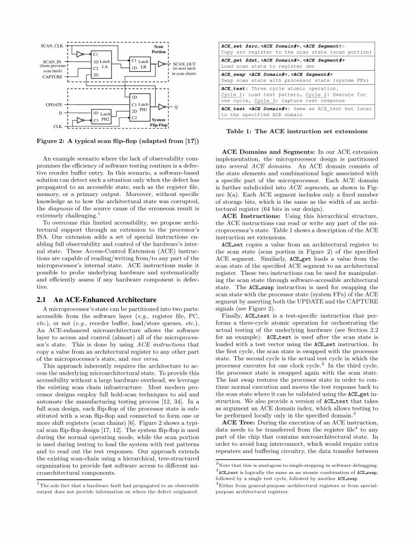
Figure 2: A typical scan flip-flop (adapted from [17])
An example scenario where the lack of observability com-promises the efficiency of software testing routines is a defec-tive reorder buffer entry. In this scenario, a software-basedsolution can detect such a situation only when the defect haspropagated to an accessible state, such as the register file,memory, or a primary output. Moreover, without specificknowledge as to how the architectural state was corrupted,the diagnosis of the source cause of the erroneous result isextremely challenging.1
To overcome this limited accessibility, we propose archi-tectural support through an extension to the processor’sISA. Our extension adds a set of special instructions en-abling full observability and control of the hardware’s inter-nal state. These Access-Control Extension (ACE) instruc-tions are capable of reading/writing from/to any part of themicroprocessor’s internal state. ACE instructions make itpossible to probe underlying hardware and systematicallyand efficiently assess if any hardware component is defec-tive.
2.1 An ACE-Enhanced ArchitectureA microprocessor’s state can be partitioned into two parts:
accessible from the software layer (e.g., register file, PC,etc.), or not (e.g., reorder buffer, load/store queues, etc.).An ACE-enhanced microarchitecture allows the softwarelayer to access and control (almost) all of the microproces-sor’s state. This is done by using ACE instructions thatcopy a value from an architectural register to any other partof the microprocessor’s state, and vice versa.
This approach inherently requires the architecture to ac-cess the underlying microarchitectural state. To provide thisaccessibility without a large hardware overhead, we leveragethe existing scan chain infrastructure. Most modern pro-cessor designs employ full hold-scan techniques to aid andautomate the manufacturing testing process [12, 34]. In afull scan design, each flip-flop of the processor state is sub-stituted with a scan flip-flop and connected to form one ormore shift registers (scan chains) [6]. Figure 2 shows a typi-cal scan flip-flop design [17, 12]. The system flip-flop is usedduring the normal operating mode, while the scan portionis used during testing to load the system with test patternsand to read out the test responses. Our approach extendsthe existing scan-chain using a hierarchical, tree-structuredorganization to provide fast software access to different mi-croarchitectural components.
1The sole fact that a hardware fault had propagated to an observable
output does not provide information on where the defect originated.
ACE_set $src,<ACE Domain#>,<ACE Segment#> Copy src register to the scan state (scan portion)
ACE_get $dst,<ACE Domain#>,<ACE Segment#>Load scan state to register dst
ACE_swap <ACE Domain#>,<ACE Segment#>Swap scan state with processor state (system FFs)
ACE_test: Three cycle atomic operation.Cycle 1: Load test pattern, Cycle 2: Execute for one cycle, Cycle 3: Capture test response
ACE_test <ACE Domain#>: Same as ACE_test but local to the specified ACE domain
Table 1: The ACE instruction set extensions
ACE Domains and Segments: In our ACE extensionimplementation, the microprocessor design is partitionedinto several ACE domains. An ACE domain consists ofthe state elements and combinational logic associated witha specific part of the microprocessor. Each ACE domainis further subdivided into ACE segments, as shown in Fig-ure 3(a). Each ACE segment includes only a fixed numberof storage bits, which is the same as the width of an archi-tectural register (64 bits in our design).
ACE Instructions: Using this hierarchical structure,the ACE instructions can read or write any part of the mi-croprocessor’s state. Table 1 shows a description of the ACEinstruction set extensions.ACE set copies a value from an architectural register to
the scan state (scan portion in Figure 2) of the specifiedACE segment. Similarly, ACE get loads a value from thescan state of the specified ACE segment to an architecturalregister. These two instructions can be used for manipulat-ing the scan state through software-accessible architecturalstate. The ACE swap instruction is used for swapping thescan state with the processor state (system FFs) of the ACEsegment by asserting both the UPDATE and the CAPTUREsignals (see Figure 2).
Finally, ACE test is a test-specific instruction that per-forms a three-cycle atomic operation for orchestrating theactual testing of the underlying hardware (see Section 2.2for an example). ACE test is used after the scan state isloaded with a test vector using the ACE set instruction. Inthe first cycle, the scan state is swapped with the processorstate. The second cycle is the actual test cycle in which theprocessor executes for one clock cycle.2 In the third cycle,the processor state is swapped again with the scan state.The last swap restores the processor state in order to con-tinue normal execution and moves the test response back tothe scan state where it can be validated using the ACE get in-struction. We also provide a version of ACE test that takesas argument an ACE domain index, which allows testing tobe performed locally only in the specified domain.3
ACE Tree: During the execution of an ACE instruction,data needs to be transferred from the register file4 to anypart of the chip that contains microarchitectural state. Inorder to avoid long interconnect, which would require extrarepeaters and buffering circuitry, the data transfer between
2Note that this is analogous to single-stepping in software debugging.
3ACE test is logically the same as an atomic combination of ACE swap,
followed by a single test cycle, followed by another ACE swap.4Either from general-purpose architectural registers or from special-
purpose architectural registers.
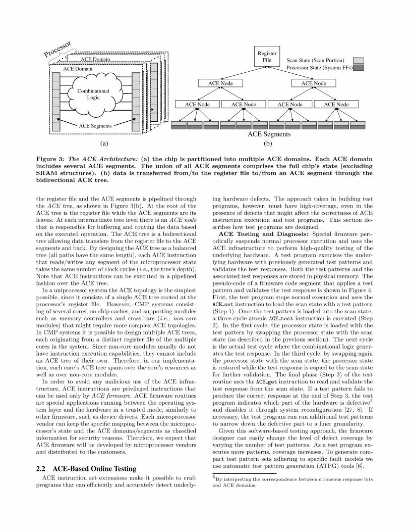
(a) (b)
Combinational Logic
ACE Segments
ACE Domain
Combinational Logic
ACE Segments
ACE Domain
Combinational Logic
ACE Segments
ACE Domain
Combinational Logic
ACE Segments
ACE Domain
Combinational Logic
ACE Segments
ACE Domain
Combinational Logic
ACE Segments
ACE Domain
RegisterFile
ACE Node
ACE Node ACE Node ACE Node ACE Node
ACE Node
ACE Segments
Scan State (Scan Portion)Processor State (System FFs)
Figure 3: The ACE Architecture: (a) the chip is partitioned into multiple ACE domains. Each ACE domainincludes several ACE segments. The union of all ACE segments comprises the full chip’s state (excludingSRAM structures). (b) data is transferred from/to the register file to/from an ACE segment through thebidirectional ACE tree.
the register file and the ACE segments is pipelined throughthe ACE tree, as shown in Figure 3(b). At the root of theACE tree is the register file while the ACE segments are itsleaves. At each intermediate tree level there is an ACE node
that is responsible for buffering and routing the data basedon the executed operation. The ACE tree is a bidirectionaltree allowing data transfers from the register file to the ACEsegments and back. By designing the ACE tree as a balancedtree (all paths have the same length), each ACE instructionthat reads/writes any segment of the microprocessor statetakes the same number of clock cycles (i.e., the tree’s depth).Note that ACE instructions can be executed in a pipelinedfashion over the ACE tree.
In a uniprocessor system the ACE topology is the simplestpossible, since it consists of a single ACE tree rooted at theprocessor’s register file. However, CMP systems consist-ing of several cores, on-chip caches, and supporting modulessuch as memory controllers and cross-bars (i.e., non-core
modules) that might require more complex ACE topologies.In CMP systems it is possible to design multiple ACE trees,each originating from a distinct register file of the multiplecores in the system. Since non-core modules usually do nothave instruction execution capabilities, they cannot includean ACE tree of their own. Therefore, in our implementa-tion, each core’s ACE tree spans over the core’s resources aswell as over non-core modules.
In order to avoid any malicious use of the ACE infras-tructure, ACE instructions are privileged instructions thatcan be used only by ACE firmware. ACE firmware routinesare special applications running between the operating sys-tem layer and the hardware in a trusted mode, similarly toother firmware, such as device drivers. Each microprocessorvendor can keep the specific mapping between the micropro-cessor’s state and the ACE domains/segments as classifiedinformation for security reasons. Therefore, we expect thatACE firmware will be developed by microprocessor vendorsand distributed to the customers.
2.2 ACE-Based Online TestingACE instruction set extensions make it possible to craft
programs that can efficiently and accurately detect underly-
ing hardware defects. The approach taken in building testprograms, however, must have high-coverage, even in thepresence of defects that might affect the correctness of ACEinstruction execution and test programs. This section de-scribes how test programs are designed.
ACE Testing and Diagnosis: Special firmware peri-odically suspends normal processor execution and uses theACE infrastructure to perform high-quality testing of theunderlying hardware. A test program exercises the under-lying hardware with previously generated test patterns andvalidates the test responses. Both the test patterns and theassociated test responses are stored in physical memory. Thepseudo-code of a firmware code segment that applies a testpattern and validates the test response is shown in Figure 4.First, the test program stops normal execution and uses theACE set instruction to load the scan state with a test pattern(Step 1). Once the test pattern is loaded into the scan state,a three-cycle atomic ACE test instruction is executed (Step2). In the first cycle, the processor state is loaded with thetest pattern by swapping the processor state with the scanstate (as described in the previous section). The next cycleis the actual test cycle where the combinational logic gener-ates the test response. In the third cycle, by swapping againthe processor state with the scan state, the processor stateis restored while the test response is copied to the scan statefor further validation. The final phase (Step 3) of the testroutine uses the ACE get instruction to read and validate thetest response from the scan state. If a test pattern fails toproduce the correct response at the end of Step 3, the testprogram indicates which part of the hardware is defective5
and disables it through system reconfiguration [27, 8]. Ifnecessary, the test program can run additional test patternsto narrow down the defective part to a finer granularity.
Given this software-based testing approach, the firmwaredesigner can easily change the level of defect coverage byvarying the number of test patterns. As a test program ex-ecutes more patterns, coverage increases. To generate com-pact test pattern sets adhering to specific fault models weuse automatic test pattern generation (ATPG) tools [6].
5By interpreting the correspondence between erroneous response bits
and ACE domains.

Step 1: Test Pattern Loading
// load test pattern to scan statefor(i=0;i<#_of_ACE_Domains;i++){for(j=0;j<#_of_ACE_Segments;j++){load $r1,pattern_mem_locACE_set $r1, i, jpattern_mem_loc++
}
Step 2: Testing
// Three cycle operation// 1)load test pattern // to processor state// 2)execute for one cycle// 3)capture test response &// restore processor stateACE_test
Step 3: Test Response Validation
// validate test responsefor(i=0;i<#_of_ACE_Domains;i++){for(j=0;j<#_of_ACE_Segments;j++){load $r1,test_resp_mem_locACE_get $r2, i, jif ($r1!=$r2) then ERROR elsetest_resp_mem_loc++
}
Figure 4: ACE firmware: Pseudo-code for 1) loading a test pattern, 2) testing, and 3) validating the response.
Basic Core Functional Testing: When performingACE-based testing, there is one initial challenge to over-come: ACE-based testing firmware relies on the correctnessof a set of basic core functionalities which load test patterns,execute ACE instructions, and validate the test response. Ifthe core has a defect that prevents the correct execution ofthe ACE firmware, then ACE testing cannot be performedreliably. To bypass this problem, we craft specific programsto test the basic functionalities of a core before running anyACE testing firmware. If these programs do not report suc-cess in a timely manner to an independent auditor (e.g., theoperating system running on the other cores), then we as-sume that an irrecoverable defect has occurred on the coreand we permanently disable it. If the basic core functionali-ties are found to be intact, finer-grained ACE-based testingcan begin. Although these basic functionality tests do notprovide high-quality testing coverage, they provide enoughcoverage to determine if the core can execute the targetedACE testing firmware with a very high probability. A sim-ilar technique employing software-based functional testingwas used for the manufacturing testing of Pentium 4 [21].
Testing Frequency: Device experts suggest that themajority of wearout-related defects manifest themselves asprogressively slow devices before eventually leading to a per-manent breakdown [3, 13]. Therefore, the initial observablesymptoms of most wearout-related defects are timing vio-lations. To detect such wearout-related defects early, weemploy a test clock frequency that is slightly faster thanthe operating frequency. We extend the existing dynamicvoltage/frequency scaling mechanisms employed in modernprocessors [15] to support a frequency that is slightly higherthan the fastest used during normal operation.6
2.3 ACE Testing in a Checkpointingand Recovery Environment
We incorporate the ACE testing framework within a mul-tiprocessor checkpointing and recovery mechanism (e.g.,SafetyNet [31] or ReVive [22]) to provide support for system-level recovery. When a defect is detected, the system stateis recovered to the last checkpoint (i.e., correct state) afterthe system is repaired.
In a checkpoint/recovery system, the release of a check-point is an irreversible action. Therefore, the system mustexecute the ACE testing firmware at the end of each check-point interval to test the integrity of the whole chip. Acheckpoint is released only if ACE testing finds no defects.With this policy, the performance overhead induced by run-
6The safeguard margins used in modern microprocessors (to tolerate
process variation) allow the use of a slightly faster testing frequency
with a negligible number of false positives [9].
ning the ACE testing firmware depends directly on thelength of the checkpoint interval, that is, longer intervalslead to lower performance overhead. We explore the trade-off between checkpoint interval size and ACE testing perfor-mance overhead in Section 4.5.
To achieve long checkpoint intervals, I/O operations needto be handled carefully. I/O operations such as filesys-tem/monitor writes or network packet transmissions are ir-reversible actions and can force an early checkpoint termi-nation. To avoid premature terminations, we buffer I/Ooperations as proposed in [19]. Alternatively, the operatingsystem can be modified to allow speculative I/O operationsas described in [20], an option we have not explored.
2.4 Flexibility of ACE TestingThe software nature of ACE-based testing inherently pro-
vides a more flexible solution than hardwired solutions. Themajor advantages offered by this flexibility are:
Dynamic tuning of the performance-reliabilitytrade-off: The software nature of ACE testing providesthe ability to dynamically trade-off performance with reli-ability (defect coverage). For example, when the system isrunning a critical application demanding high system reli-ability, ACE testing firmware can be run more frequentlywith higher quality and higher coverage targets (i.e., useof different fault models and more test patterns). On theother hand, when running a performance critical applica-tion with relatively low reliability requirements (e.g., mpegdecompression), the ACE testing frequency can be reduced.
Utilization-oriented testing: ACE testing allows thesystem to selectively test only those resources utilized by therunning applications. For example, if the system is runninginteger-intensive applications, there might be no need to testunutilized FPU resources.
Upgradability: Both fault models and ATPG tools areactive research areas. Researchers continuously improve thequality and coverage of the generated test patterns. There-fore, during the lifetime of a processor, numerous advanceswill improve the quality and test coverage of the ATPG pat-terns. The software nature of ACE testing allows processorvendors to periodically issue ACE firmware updates that canincorporate these advances, and thus improve the defect de-tection quality during the processor’s lifetime.
Adaptability: ACE testing allows vendors to adapt thetesting method based on in-the-field analysis of likely defectscenarios. For example, if a vendor observes that the failureof a specific processor is usually originating from a partic-ular module, they can adapt the ACE testing firmware toprioritize efforts on that particular module.

�������
����
�������
�����
�������
�����
�������
�����
����
�����
����
������
����
������
����
������
����
������
����
������
����
������
����
������
������
����
������
�����
������
�����
������
�����
��� �������
����
�� �
!��
����"##
����
����"##
���������"##
�����
����"##
�����
���$
��%�&�
���$
��%��&�
'�
�� (��
)��
�����
������
������
������
Modules covered by ACEModules not covered by ACE
Figure 5: ACE coverage of the OpenSPARC T1
processor: Modules that are dominated by SRAMstructures, such as on-chip caches, are not coveredby ACE testing since they are already protected byECC.
3. Experimental MethodologyTo evaluate our software-based defect detection technique
we used the OpenSPARC T1 architecture, the open sourceversion of the commercial UltraSPARC T1 (Niagara) pro-cessor from Sun [33], as our experimental testbed.
The OpenSPARC T1 processor implements the 64-bitSPARC V9 architecture and targets commercial applicationssuch as application servers and database servers. It containseight SPARC processor cores, each with full hardware sup-port for four threads. The eight cores are connected througha crossbar to a unified L2 cache (3MB). The chip also in-cludes four memory controllers and a shared FPU unit [33].
First, using the processor’s RTL code, we divided the pro-cessor into ACE domains. We made this partition based onfunctionality, where each domain comprises a basic function-ality module in the RTL code. When dividing the processorinto ACE domains we excluded modules that are dominatedby SRAM structures (such as caches) because such modulesare already protected with error-coding techniques such asECC. Figure 5 shows the processor modules covered by theACE framework (note that the L1 caches within each coreare also excluded). Overall, our RTL implementation of theACE framework consists of 79 ACE domains, each domainincluding on average 45 64-bit ACE segments. The wholechip comprises roughly 235K ACE-accessible bits.
Next, we used the Synopsys Design Compiler to synthesizeeach ACE domain using the Artisan IBM 0.13um standardcell library. We used the Synopsys TetraMAX ATPG toolto generate the test patterns. TetraMAX takes as inputthe gate-level synthesized design, a fault model, and a testcoverage target and tries to generate the minimum set oftest patterns that meet the test coverage target.
Fault Models: In our studies we explored several single-fault models: stuck-at, N-detect and path-delay. The stuck-at fault model is the industry standard model for test pat-tern generation. It assumes that a circuit defect behaves as anode stuck at 0 or 1. However, previous research has shownthat the test pattern sets generated using the N-detect faultmodel are more effective for both timing and hard failures,
and present higher correlation to actual circuit defects [16,10]. In the N-detect test pattern sets, each single stuck-at fault is detected by at least N different test patterns.As expected, the benefit of more effective testing by usingthe N-detect model comes with the overhead of larger testpattern set sizes and longer testing times. To provide theflexibility of dynamically trading off between reliability andperformance, we generate test pattern sets using both faultmodels.
In addition to the stuck-at and N-detect fault models, wealso generate test pattern sets using the path-delay faultmodel [6]. This fault model tests the design for delay faultsthat can cause timing violations. The test patterns gener-ated using the path-delay fault model exercise the circuit’spaths at-speed to detect whether a path is too slow due tomanufacturing defects, wearout-related defects, or processvariation.
Benchmarks: We used a set of benchmarks from theSPEC CPU2000 suite to evaluate the performance over-head and memory logging requirements of ACE testing. Allbenchmarks were run with the reference input set.
Microarchitectural Simulation: To evaluate the per-formance overhead of ACE testing, we modified the SESCsimulator [25] to simulate a SPARC core enhanced with theACE framework. The simulated SPARC core is a 6-stage,in-order core (with 16KB IL1 and 8KB DL1 caches) runningat 1GHz [33].7 For each simulation run, we skipped the firstbillion instructions and then performed cycle-accurate sim-ulation for different checkpoint interval lengths (10M, 100Mand 1B dynamic instructions). To obtain the number ofclock cycles needed for ACE testing, we simulated a processthat was emulating the ACE testing functionality.
Experiments to Determine Memory Logging Re-quirements: To evaluate the memory logging storage re-quirements of coarse-grained checkpointing, we used the Pinx86 binary instrumentation tool [14]. We wrote a Pin toolthat measures the storage needed to buffer the cache lineswritten back from the L2 cache to main memory duringa checkpoint interval, based on the ReVive checkpointingscheme [22]. Note that only the first L2 writeback to amemory address during the checkpoint interval causes theold value of the cache line to be logged in the buffer. 64bytes (same as our cache line size) are logged for each L2writeback. Benchmarks were run to completion for theseexperiments.
RTL Implementation: We implemented the ACE treestructure in RTL using Verilog in order to obtain a de-tailed and accurate estimate of the area overhead of theACE framework. We synthesized our design of the ACEtree using the same tools, cell library and methodology thatwe used for synthesizing the OpenSPARC T1 modules, asdescribed earlier in this section.
4. Experimental Evaluation4.1 Basic Core Functional Testing
Before running the ACE testing firmware, we first run asoftware functional test to check the core for defects thatwould prevent the correct execution of the testing firmware.If this test does not report success in a timely manner to anindependent auditor (i.e., the OS running on other cores),
7SESC provides a configuration file for the OpenSPARC T1 proces-
sor, which we used in our experiments.

Memory Error (6.49%)
Illegal Execution (1.40%)
Early Termination
(0.49%)
Execution Timeout (1.57%)
Control Flow Assertion (7.45%)
Register Access
Assertion (23.36%)
Incorrect Execution Assertion (21.38%)
Undetected Faults
(37.86%)
Control Flow Assertion Incorrect execution during the control flow test.
Register Access Assertion Incorrect execution during the register access test.
Incorrect Execution Assertion The final result of the test is incorrect.
Early Termination The execution terminated without executing all the instructions (wrong control flow)
Execution Timeout The test executed for more than the required clock cycles (wrong control flow, e.g., infinite loop)
Illegal Execution The test executed an illegal instruction (e.g., aninstruction with an invalid opcode)
Memory Error Memory request for an invalid memory address
Undetected Fault The test executed correctly
Figure 6: Fault coverage of basic core functional testing: The pie chart on the right shows the distributionof the outcomes of a fault injection campaign on a 5-stage in-order core running the purely software-basedpreliminary functional tests.
the test is repeated to verify that the failing cause was nottransient. If the test fails again then an irrecoverable coredefect is assumed, the core is disabled, and the targeted testsare canceled.
The software functional test we used to check the core con-sists of three self-validating phases. The first phase runs abasic control flow check where 64 basic blocks are executedin a non-sequential control flow and each of the 64 basicblocks sets the value of a bit in a 64-bit architectural regis-ter. At the end of the phase, a control flow assertion checksthe value of the register to determine whether or not theexecution was correct. The second phase checks the core’scapability to access the register file. This phase consists ofa sequence of data-dependent ALU instructions that even-tually read and write all architectural registers. At the endof this phase, the final result of this chain of computation ischecked by an assertion. The final phase of the basic coretest consists of a sequence of dependent instructions thatuses each of the instructions in the ISA at least once. Thefinal result of the functional test is checked by an assertionthat validates the last generated value. The total size of thesoftware functional test is about 700 dynamic instructions.
To evaluate the effectiveness of the basic core test, we per-formed a stuck-at fault injection campaign on the gate-levelnetlist of a synthesized 5-stage in-order core (similar to theSPARC core with the exception of multithreading support).Figure 6 shows the distribution of the outcomes of the faultinjection campaign. Overall, basic core test successfully de-tected 62.14% of the injected faults. The remaining 37.86%of the injected faults lied in parts of the core’s logic that donot affect the core’s capability of executing simple programssuch as the basic core test and the ACE testing firmware.ACE testing firmware will subsequently test these untestedareas of the design to provide full core coverage.
These results also demonstrate that software-based func-tional tests that, unlike the ACE testing firmware, do nothave access/control on the core’s internal state, are inade-quate to provide a high-quality, high-coverage test of theunderlying hardware. Similar software functional testingtechniques were used for the manufacturing testing of theIntel Pentium 4 [21]. The coverage of these tests as reportedin [21] is in the range of 70% which corroborates the resultswe observed from our fault-injection campaign on a simplerNiagara-based core.
4.2 ACE Testing Latency and CoverageAn important metric for measuring the efficiency of our
technique is how long it takes to fully check the underly-ing hardware for defects. The latency of testing an ACEdomain depends on (1) the number of ACE segments it con-sists of and (2) the number of test patterns that need tobe applied. In this experiment, we generate test patternsfor each individual ACE domain in the design using threedifferent fault models (stuck-at, path-delay and N-detect)and the methodology described in Section 3. Table 2 liststhe number of test instructions needed to test each of themajor modules in the design (based on the ACE firmwarecode shown in Figure 4).
For the stuck-at fault model, the most demanding mod-ule is the SPARC core, requiring about 150K dynamic testinstructions to complete the test. Modules dominated bycombinational logic, such as the SPARC core, the DRAMcontroller, the FPU, and the I/O bridge are more demand-ing in terms of test instructions. On the other hand, theCPU-cache crossbar that consists mainly of buffer queuesand interconnect requires much fewer instructions to com-plete the tests.
For the path-delay fault model, we generate test patternsets for the critical paths that are within 5% of the clock pe-riod. The required number of test instructions to completethe path-delay tests is usually less than or similar to thatrequired by the stuck-at model. Note that, with these path-delay test patterns, a defective device can cause undetectedtiming violations only if it is not in any of the selected crit-ical paths and it causes extra delays greater than 5% of theclock period. We believe that this probability is extremelylow, however, stricter path selection strategies can providehigher coverage if deemed necessary (with a higher testinglatency). In our design we found that our path selectionstrategy does not lead to a large number of selected paths.However, in designs where delays of the majority of pathsare within 5% of the clock period, more sophisticated pathselection strategies can keep the number of selected pathslow while maintaining high test coverage [18].
For the N-detect fault model, the number of test instruc-tions is significantly more than that needed for the stuck-atmodel. This is because many more test patterns are neededto satisfy the N-detect requirement. For values of N higherthan four, we observed that the number of test patterns gen-

Module Area (mm2) ACE Accessible Bits
Stuck-at Test Insts
Test Coverage (%)
Path-Delay Test Insts
N-detect Test Insts N = 2 N = 4
SPARC CPU Core (sparc) 8x17=136 8x19772=158176 152370 100.00 110985 234900 434382 CPU-Cache Crossbar (ccx) 14.0 27645 67788 100.00 10122 117648 200664 Floating Point Unit (fpu) 4.6 4620 88530 99.95 31374 126222 212160 e-Fuse Cluster (efc) 0.2 292 11460 94.70 4305 33000 68160 Clock and Test Unit (ctu) 2.3 4205 68904 92.88 10626 126720 240768 I/O Bridge (iobdg) 4.9 10775 110274 100.00 31479 171528 316194 DRAM controller (dram_ctl) 2x6.95=13.9 2x14201=28402 122760 91.44 126238 204312 365364 Total 175.9 234115 99.22 �
�
�
�
�
�
�
�
�
�
�
�
�
�
�
�
�
�
�
�
�
�
�
�
�
�
�
�
�
�
�
�
�
�
�
�
�
�
Table 2: Number of test instructions needed to test each of the major modules in the design.�
Module Cores [0,1] Test Insts Cores [2,4] Test Insts Cores [3,5] Test Insts Cores [6,7] Test Insts Stuck-at Path-delay Stuck-at Path-delay Stuck-at Path-delay Stuck-at Path-delay
1 x SPARC CPU Core 152370 110985 152370 110985 152370 110985 152370 110985 1/8 x CPU-Cache Crossbar 8474 1265 8474 1265 8474 1265 8474 1265 1/2 x Floating Point Unit 44265 15687 1/2 x e-Fuse Cluster 5730 2153 1/2 x Clock and Test Unit 34452 5313 1/2 x I/O Bridge 55137 15740 1/2 x DRAM controller (pair) 61380 63119 61380 63119 Total 195296 117563 277361 191109 227954 177522 205109 127937 Stuck-at + Path-delay total 312859 468470 405476 333046
�
�
�
�
�
Table 3: Number of test instructions needed by each core pair in full-chip distributed testing: The testingprocess is distributed over the chip’s eight SPARC cores. Each core is assigned to test its resources and someparts of the surrounding non-core modules as shown in this table.
erated increases almost linearly with N, an observation thatis aligned with previous studies [16, 10].
Full Test Coverage: The overall chip test coverage forthe stuck-at fault model is 99.22% (shown in Table 2). Theonly modules that exhibit test coverage lower than 99.9% arethe e-Fuse cluster, the clock and test unit, and the DRAMcontrollers, which exhibit the lowest test coverage at 91.44%.The relatively low test coverage in these modules is due toATPG untestability of some portions of the combinationallogic. In other words, no test patterns exist that can seta combinational node to a specific value (lack of controlla-bility), or propagate a combinational node’s value to an ob-servable node (lack of observability). If necessary, a designercan eliminate this shortcoming by adding dummy intermedi-ate state elements in the circuit to enable controllability andobservability of the ATPG untestable nodes. The test cov-erage for the two considered N-detect fault models is slightlyless than that of the stuck-at model, at 98.88% and 98.65%,respectively (not shown in Table 2 for simplicity).
4.3 Full-Chip Distributed TestingIn the OpenSPARC T1 architecture, the hardware test-
ing process can be distributed over the chip’s eight SPARCcores. Each core has an ACE tree that spans over the core’sresources and over parts of the surrounding non-core mod-ules (e.g., the CPU-cache crossbar, the DRAM controllersetc.). Therefore, each core is assigned to test its resourcesand some parts of the surrounding non-core modules.
We distributed the testing responsibilities of the non-coremodules to the eight SPARC cores based on the physicallocation of the modules on the chip (shown in Figure 5).Table 3 shows the resulting distribution. For example, eachof the cores zero and one are responsible for testing a fullSPARC core, one eighth of the CPU-cache crossbar and onehalf of the clock and test unit. Therefore, cores zero and
one need 195K dynamic test instructions to test for stuck-at faults and 117K instructions to test for path-delay faultsin the parts of the chip they are responsible for. Note thatthe ACE tree of a core is designed such that it covers all thenon-core areas that the core is responsible for testing.
The most heavily loaded pair of cores are cores two andfour. Each of these two cores is responsible for testing itsown resources, one eighth of the CPU-cache crossbar, onehalf of the DRAM controller and one half of the I/O bridge,for a total of 468K dynamic test instructions (for both stuck-at and path-delay testing). The overall latency required tocomplete the testing of the entire chip is driven by these468K dynamic test instructions, since all the other coreshave shorter test sequences and will therefore complete theirtests sooner.
4.4 Memory Logging Requirements ofCoarse-grained Checkpointing
The performance overhead induced by running the ACEtesting firmware depends on the testing firmware’s execu-tion time and execution frequency. When ACE testing iscoupled with a checkpointing and recovery mechanism, inorder to reduce its execution frequency, and therefore itsperformance overhead, coarse-grained checkpointing inter-vals are required.
Figure 7 explores the memory logging storage require-ments for such coarse-grained checkpointing intervals on theexamined SPEC CPU2000 benchmarks. The memory logsize requirements are shown for a system with a 2MB L2data cache (recall that memory logging is performed onlyfor the first L2 writeback of a cacheline to main memory in acheckpoint interval [22]). For each benchmark, we show theaverage and maximum required memory log size for intervalsof 10 million, 100 million and 1 billion executed instructions.The maximum metric keeps track of the maximum memory

1.0E+00
1.0E+01
1.0E+02
1.0E+03
1.0E+04
1.0E+05
1.0E+06
1.0E+07
1.0E+08
1.0E+09
10M
100M 1B
10M
100M 1B
10M
100M 1B
10M
100M 1B
10M
100M 1B
10M
100M 1B
10M
100M 1B
10M
100M 1B
10M
100M 1B
10M
100M 1B
10M
100M 1B
10M
100M 1B
10M
100M 1B
ammp apsi art equake mesa mgrid sixtrack swim bzip2 gcc gzip mcf parser
Mem
ory
Log S
ize (B
ytes
)
Checkpoint Interval (Instructions) - Benchmarks
MaximumAverage
Figure 7: Memory logging storage requirements: Average and maximum memory log size requirements forcheckpoint intervals of 10 million, 100 million and 1 billion executed instructions.
0
5
10
15
20
25
30
35
sasa
+pd
n2+p
dn4
+pd sa
sa+p
dn2
+pd
n4+p
d sasa
+pd
n2+p
dn4
+pd sa
sa+p
dn2
+pd
n4+p
d sasa
+pd
n2+p
dn4
+pd sa
sa+p
dn2
+pd
n4+p
d sasa
+pd
n2+p
dn4
+pd sa
sa+p
dn2
+pd
n4+p
d sasa
+pd
n2+p
dn4
+pd sa
sa+p
dn2
+pd
n4+p
d sasa
+pd
n2+p
dn4
+pd sa
sa+p
dn2
+pd
n4+p
d sasa
+pd
n2+p
dn4
+pd
ammp art bzip2 crafty equake gcc gzip mcf mesa parser twolf vpr Average
Perf
orm
ance
Ove
rhea
d (%
) sa - Stuck-atpd - Path Delayn2 - N-Detect (N=2)n4 - N-Detect (N=4)
Figure 8: Performance overhead of ACE testing for a 100M instructions checkpoint interval.
log size required in any of the checkpoint intervals duringthe benchmark’s execution, while the average metric aver-ages the memory log size requirement over all the checkpointintervals (note that the benchmarks were ran to completionwith the reference inputs).
We observe that when considering checkpoint intervalsthat are in the order of 100 million executed instructions,the average memory log size requirements are in the rangeof a few kilobytes to 10MB. The most demanding bench-mark is swim: on average it requires 1.8MB, 10MB and91.4MB respectively for checkpoint intervals of 10M, 100Mand 1B instructions. Since the memory log will be main-tained at the system’s physical memory, the results of thisexperiment suggest that checkpoint intervals of hundredsof millions of executed instructions are sustainable with in-significant memory storage overhead.8
4.5 Performance Overhead of ACE TestingFigure 8 shows the performance overhead of ACE testing
when the checkpoint interval is set to 100M instructions.At the end of each checkpoint interval, normal execution issuspended and ACE testing is performed. In these exper-
8Note that most current systems are equipped with at least 2GB of
physical memory.
iments, the ACE testing firmware executes until it reachesthe maximum test coverage. The four bars show the perfor-mance overhead when the fault model used in ACE testing isi) stuck-at, ii) stuck-at and path-delay, iii) N-detect (N=2)and path-delay, and iv) N-detect (N=4) and path-delay.
The minimum average performance overhead of ACE test-ing is 5.5% and is observed when only the industry-standardstuck-at fault model is used. When the stuck-at fault modelis combined with the path-delay fault model to achievehigher testing quality, the average performance overhead in-creases to 9.8%. When test pattern sets are generated usingthe N-detect fault model, the average performance overheadis 15.2% and 25.4%, for N=2 and N=4 respectively.
Table 4 shows the trade-off between memory logging stor-age requirements and performance overhead for checkpointintervals of 10M, 100M and 1B dynamic instructions. Bothlog size and performance overhead are averaged over all eval-uated benchmarks. As the checkpoint interval size increases,the required log size increases, but the performance overheadof ACE testing decreases. We conclude that checkpoint in-
tervals in the order of hundreds of millions of instructions
are sustainable with reasonable storage overhead, while pro-
viding an efficient substrate to perform ACE testing with low
performance overhead.
(a) (b)
0
1
2
3
4
5
6
88 89 90 91 92 93 94 95 96 97 98 99 100
Perf
orm
ance
Ove
rhea
d (%
)
Test Coverage (%)
cores-[0,1]
cores-[2,4]cores-[3,5]
cores-[6,7]cores-[6,7]
020000400006000080000
100000120000140000160000
88 89 90 91 92 93 94 95 96 97 98 99 100
Test
Inst
ruct
ions
Test Coverage (%)
sparcdram_ctl
ctuccx
iobdg
fpu
efc
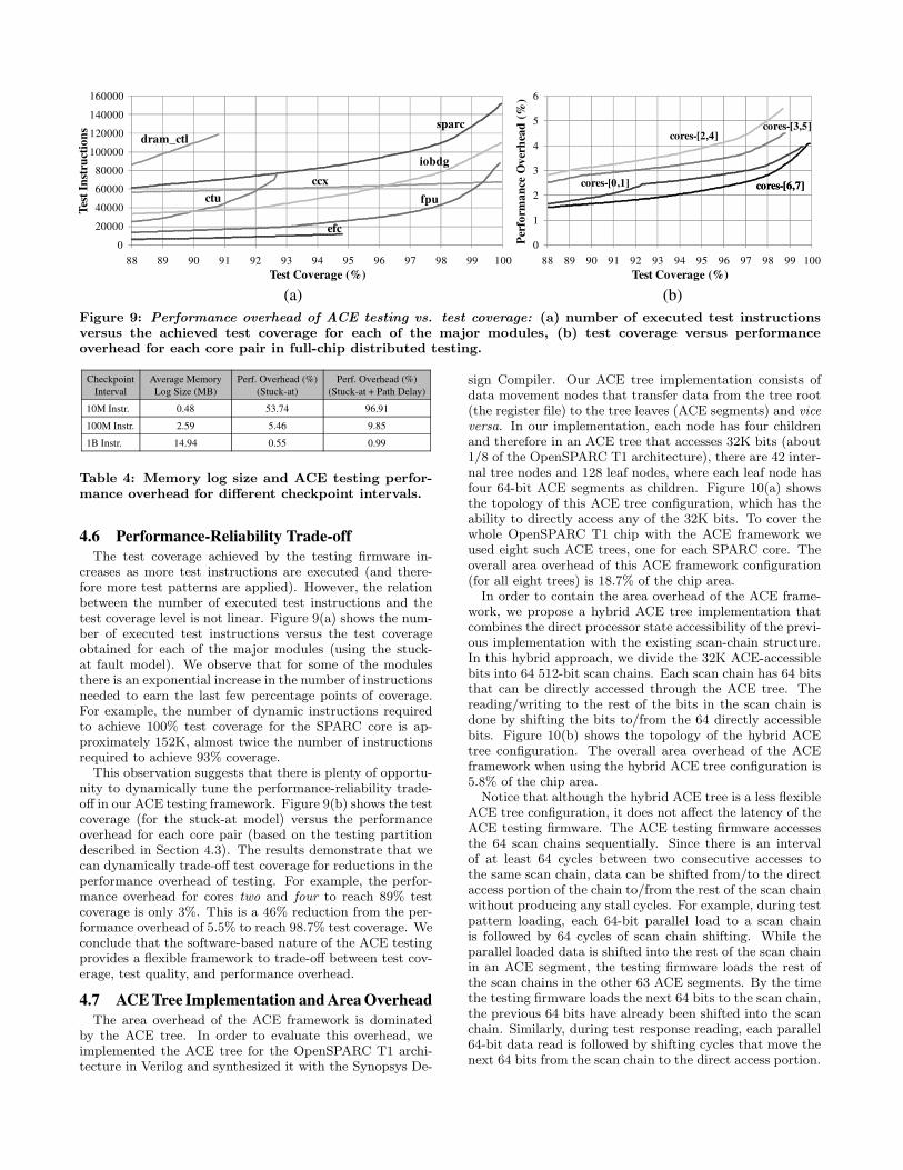
Figure 9: Performance overhead of ACE testing vs. test coverage: (a) number of executed test instructionsversus the achieved test coverage for each of the major modules, (b) test coverage versus performanceoverhead for each core pair in full-chip distributed testing.
Checkpoint Interval
Average Memory Log Size (MB)
Perf. Overhead (%) (Stuck-at)
Perf. Overhead (%) (Stuck-at + Path Delay)
10M Instr. 0.48 53.74 96.91100M Instr. 2.59 5.46 9.851B Instr. 14.94 0.55 0.99
Table 4: Memory log size and ACE testing perfor-mance overhead for different checkpoint intervals.
4.6 Performance-Reliability Trade-offThe test coverage achieved by the testing firmware in-
creases as more test instructions are executed (and there-fore more test patterns are applied). However, the relationbetween the number of executed test instructions and thetest coverage level is not linear. Figure 9(a) shows the num-ber of executed test instructions versus the test coverageobtained for each of the major modules (using the stuck-at fault model). We observe that for some of the modulesthere is an exponential increase in the number of instructionsneeded to earn the last few percentage points of coverage.For example, the number of dynamic instructions requiredto achieve 100% test coverage for the SPARC core is ap-proximately 152K, almost twice the number of instructionsrequired to achieve 93% coverage.
This observation suggests that there is plenty of opportu-nity to dynamically tune the performance-reliability trade-off in our ACE testing framework. Figure 9(b) shows the testcoverage (for the stuck-at model) versus the performanceoverhead for each core pair (based on the testing partitiondescribed in Section 4.3). The results demonstrate that wecan dynamically trade-off test coverage for reductions in theperformance overhead of testing. For example, the perfor-mance overhead for cores two and four to reach 89% testcoverage is only 3%. This is a 46% reduction from the per-formance overhead of 5.5% to reach 98.7% test coverage. Weconclude that the software-based nature of the ACE testingprovides a flexible framework to trade-off between test cov-erage, test quality, and performance overhead.
4.7 ACE Tree Implementation and Area OverheadThe area overhead of the ACE framework is dominated
by the ACE tree. In order to evaluate this overhead, weimplemented the ACE tree for the OpenSPARC T1 archi-tecture in Verilog and synthesized it with the Synopsys De-
sign Compiler. Our ACE tree implementation consists ofdata movement nodes that transfer data from the tree root(the register file) to the tree leaves (ACE segments) and vice
versa. In our implementation, each node has four childrenand therefore in an ACE tree that accesses 32K bits (about1/8 of the OpenSPARC T1 architecture), there are 42 inter-nal tree nodes and 128 leaf nodes, where each leaf node hasfour 64-bit ACE segments as children. Figure 10(a) showsthe topology of this ACE tree configuration, which has theability to directly access any of the 32K bits. To cover thewhole OpenSPARC T1 chip with the ACE framework weused eight such ACE trees, one for each SPARC core. Theoverall area overhead of this ACE framework configuration(for all eight trees) is 18.7% of the chip area.
In order to contain the area overhead of the ACE frame-work, we propose a hybrid ACE tree implementation thatcombines the direct processor state accessibility of the previ-ous implementation with the existing scan-chain structure.In this hybrid approach, we divide the 32K ACE-accessiblebits into 64 512-bit scan chains. Each scan chain has 64 bitsthat can be directly accessed through the ACE tree. Thereading/writing to the rest of the bits in the scan chain isdone by shifting the bits to/from the 64 directly accessiblebits. Figure 10(b) shows the topology of the hybrid ACEtree configuration. The overall area overhead of the ACEframework when using the hybrid ACE tree configuration is5.8% of the chip area.
Notice that although the hybrid ACE tree is a less flexibleACE tree configuration, it does not affect the latency of theACE testing firmware. The ACE testing firmware accessesthe 64 scan chains sequentially. Since there is an intervalof at least 64 cycles between two consecutive accesses tothe same scan chain, data can be shifted from/to the directaccess portion of the chain to/from the rest of the scan chainwithout producing any stall cycles. For example, during testpattern loading, each 64-bit parallel load to a scan chainis followed by 64 cycles of scan chain shifting. While theparallel loaded data is shifted into the rest of the scan chainin an ACE segment, the testing firmware loads the rest ofthe scan chains in the other 63 ACE segments. By the timethe testing firmware loads the next 64 bits to the scan chain,the previous 64 bits have already been shifted into the scanchain. Similarly, during test response reading, each parallel64-bit data read is followed by shifting cycles that move thenext 64 bits from the scan chain to the direct access portion.

(a) (b)
. . .. . .
. . .
Register FileLevel 0
ACE Root
ACE Leaf
64-bit ACE Segment
Level 2 16 ACE nodes
Level 1 4 ACE nodes
32K-bit 3-Level Hybrid ACE Tree with 64 scan chains
448-bit Scan Chain
ACE Node
. . .
Register File
ACE Node
Level 0 ACE RootLevel 1
2 ACE nodes
ACE Leaf
. . .
64-bit ACE Segment
Level 4 128 ACE nodes
Level 2 8 ACE nodes
Level 3 32 ACE nodes
32K-bit 5-Level Direct Access ACE Tree
Figure 10: ACE tree implementation: (a) the topology of a direct-access ACE tree. (b) the topology of ahybrid (partial direct-access, partial scan-chain) ACE tree.
5. Related WorkHardware-based Reliability Techniques: The previ-
ous work most closely related to ours is [28]. [28] proposeda hardware-based technique that utilizes microarchitecturalcheckpointing to create epochs of execution, during whichon-chip distributed BIST-like testers validate the integrityof the underlying hardware. To lower silicon cost, the testerswere customized to the tested modules. However, this leadsto increased design complexity because a specialized testerneeds to be designed for each module.
A traditional defect detection technique that is predom-inantly used for manufacturing testing is logic BIST [6].Logic BIST incorporates pseudo-random pattern generationand response validation circuitry on the chip. Although on-chip pseudo-random pattern generation removes any needfor pattern storage, such designs require a large number ofrandom patterns and often provide lower fault coverage thanATPG patterns [6].
Our work improves on these previous works due to the fol-lowing major reasons: 1) it effectively removes the need foron-chip test pattern generation and validation circuitry andmoves this functionality to software, 2) it is not hardwiredin the design and therefore has ample flexibility to be modi-fied/upgraded in the field (as described in Section 2.4), 3) ithas higher test coverage and shorter testing time because ituses ATPG instead of pseudo-randomly generated patterns;and compared to [28] 4) it can be uniformly applied to anymicroprocessor module with low design complexity becauseit does not require module-specific customizations, and 5)it provides wider coverage across the whole chip, includingnon-core modules.
Previous works proposed the creation of external circuitryfabricated from reliable devices to periodically test the hard-ware design and to reconfigure faulty parts [1, 11]. In con-trast to these works, we propose that the periodic tests beperformed by software instead (assisted by ISA extensions)in order to minimize the area cost of testing and to allowmore flexibility and adaptability.
Numerous other previous works proposed hardware-baseddefect tolerance techniques, such as [2, 4, 5]. However, theseworks focused on providing hardware-based reliability solu-tions that are limited to processing cores in uniprocessor sys-tems and do not address the testability of non-core modulesthat are abundant especially in chip-multiprocessor designs.
More recently, Smolens et al. [30] proposed a detectiontechnique for emerging wearout defects that periodically
runs functional tests that check the hardware under reducedfrequency guardbands. Their technique leverages the exist-ing scan chain hardware for generating hashed signaturesof the processor’s microarchitectural state summarizing thehardware’s response to periodic functional tests. This tech-nique allows the software to observe a signature of the mi-croarchitectural state, but it does not allow the software todirectly control (i.e., modify) the microarchitectural state.In contrast, our approach provides the software with directand fast access and control of the scan state using the ACEinfrastructure. This direct access and control capability al-lows the software to run online directed hardware tests onany part of the microarchitectural state using high-qualitytest vectors (as opposed to functional tests that do not di-rectly control the microarchitectural state and do not adhereto any fault model). Furthermore, the proposed direct fastaccess to the scan state enables the validation of each test re-sponse separately (instead of hashing and validating all thetest responses together), thereby providing finer-grained de-fect diagnosis capabilities and higher flexibility for dynamictuning between performance overhead (i.e., test length) andtest coverage.
Software-based Reliability Techniques: To ourknowledge, this is the first work that proposes a software-based technique for online hardware defect detection anddiagnosis. Only one previous work we are aware of [21] em-ployed purely software-based functional testing techniquesduring the manufacturing testing of the Intel Pentium 4 pro-cessor (see Section 2.2 for a discussion of this work). In ourapproach, we use a similar functional testing technique (our“basic core functional test” program) to check the basic corefunctionality before running the ACE firmware to performdirected, high-quality testing.
There are numerous previous works, such as [24, 26], thatproposed the use of software-based techniques for online de-tection of soft errors. However, none of them addresses theproblem of online defect detection.
Checkpointing Mechanisms: There is also a largebody of work proposing various versions of checkpointingand recovery techniques [31, 22, 19]. Both SafetyNet [31]and ReVive [22] provide general-purpose checkpointing andrecovery mechanisms for shared memory multiprocessors.Our defect detection and diagnosis technique is closely cou-pled with such techniques in providing a substrate of coarse-grained checkpoint intervals that enable efficient ACE test-ing with low performance overhead.

6. Summary & ConclusionsWe introduced a novel, flexible software-based technique,
ISA extensions, and microarchitecture support to detect anddiagnose hardware defects during online operation of a chip-multiprocessor. Our technique uses the Access-Control Ex-tension (ACE) framework that allows special ISA instruc-tions to access and control virtually any part of the proces-sor’s internal state. Based on this framework, we proposedthe use of special firmware that periodically suspends theprocessor’s execution and performs high-quality testing ofthe underlying hardware to detect defects.
Using a commercial ATPG tool and three different faultmodels, we experimentally evaluated our ACE testing tech-nique on a commercial chip-multiprocessor design based onSun’s Niagara. Our experimental results showed that ACEtesting is capable of performing high-quality hardware test-ing for 99.22% of the chip area, while itself requiring an areaoverhead of only 5.8% of the chip area based on our detailedRTL-level implementation.
We demonstrated how ACE testing can be coupled seam-lessly with a coarse-grained checkpointing and recoverymechanism to provide a complete defect tolerance solution.Our evaluation shows that, with coarse-grained checkpointintervals, the average performance overhead of ACE testingis only 5.5%. Our results also show that the software-basednature of ACE testing provides ample flexibility to dynam-ically tune the performance-reliability trade-off at runtimebased on system requirements.
7. Future DirectionsLooking forward, we believe that the ACE framework is a
very general framework that can be helpful in several otherapplications to amortize its cost. Here, we briefly list twoof the possible applications of the ACE framework we arecurrently investigating:
Post-silicon Debugging: With device scaling enter-ing the nanometer regime, traditional techniques used forpost-silicon debugging are becoming less viable. Recentlyproposed solutions have considerable area overheads andstill do not provide complete accessibility to the processor’sstate [23]. We believe the ACE framework can be an attrac-tive low-overhead framework that provides the post-silicondebug engineers with full accessibility and controllability ofthe processor’s internal state at runtime.
Manufacturing Testing: Today, the processor manu-facturing testing process uses automatic test equipment andscan chains for testing the manufactured parts. However,the testers are costly, and they have a limited number ofchannels designed to drive the scan chains and the patternloading speed is limited by the maximum scan frequency.We believe that the use of the ACE infrastructure for ap-plying test patterns to the design under test can improveboth the speed and the cost of the manufacturing testingprocess.
Acknowledgments: This work was supported by grantsfrom NSF, SRC and GSRC.
References[1] R. Alverson, D. Callahan, D. Cummings, B. Koblenz,
A. Porterfield, and B. Smith. The Tera computer system. InICS-4, pages 1–6, June 1990.
[2] T. M. Austin. DIVA: A reliable substrate for deep submicronmicroarchitecture design. In MICRO-32, pages 196–207, 1999.
[3] S. Borkar, T. Karnik, and V. De. Design and reliabilitychallenges in nanometer technologies. In DAC-41, 2004.
[4] F. A. Bower, P. G. Shealy, S. Ozev, and D. J. Sorin. Toleratinghard faults in microprocessor array structures. In DSN, 2004.
[5] F. A. Bower, D. J. Sorin, and S. Ozev. A mechanism for onlinediagnosis of hard faults in microprocessors. In MICRO, 2005.
[6] M. L. Bushnell and V. D. Agrawal. Essentials of ElectronicTesting for Digital, Memory and Mixed-Signal VLSI Circuits.Kluwer Academic Publishers, Boston, 2000.
[7] K. Constantinides, J. Blome, S. Plaza, B. Zhang, V. Bertacco,S. Mahlke, T. Austin, and M. Orshansky. BulletProof: Adefect-tolerant CMP switch architecture. In HPCA-12, 2006.
[8] W. J. Dally et al. The reliable router: A reliable andhigh-performance communication substrate for parallelcomputers. In PCRCW, pages 241–255, 1994.
[9] D. Ernst et al. Razor: A low-power pipeline based oncircuit-level timing speculation. In MICRO-36, 2003.
[10] R. Guo, S. Mitra, E. Amyeen, J. Lee, S. Sivaraj, andS. Venkataraman. Evaluation of test metrics: Stuck-at, bridgecoverage estimate and gate exhaustive. In VTS, 2006.
[11] J. R. Heath et al. A defect-tolerant computer architecture:Opportunities for nanotechnology. Science, 280(5370), 1998.
[12] R. Kuppuswamy et al. Full hold-scan systems inmicroprocessors: Cost/benefit analysis. Intel TechnologyJournal (ITJ), 8(1):63–72, Feb. 2004.
[13] Y.-H. Lee et al. Prediction of logic product failure due tothin-gate oxide breakdown. In IRPS-44, 2006.
[14] C.-K. Luk et al. Pin: Building customized program analysistools with dynamic instrumentation. In PLDI, 2005.
[15] G. Magklis et al. Profile-based dynamic voltage and frequencyscaling for a multiple clock domain microprocessor. InISCA-30, June 2003.
[16] E. J. McCluskey and C.-W. Tseng. Stuck-fault tests vs. actualdefects. In ITC, pages 336–343, Oct. 2000.
[17] S. Mitra, N. Seifert, M. Zhang, Q. Shi, and K. S. Kim. Robustsystem design with built-in soft-error resilience. Computer,38(2):43–52, Feb. 2005.
[18] A. Murakami et al. Selection of potentially testable path delayfaults for test generation. In ITC, pages 376–384, Oct. 2000.
[19] J. Nakano, P. Montesinos, K. Gharachorloo, and J. Torrellas.ReViveI/O: Efficient handling of I/O in highly-availablerollback-recovery servers. In HPCA-12, 2006.
[20] E. B. Nightingale, P. M. Chen, and J. Flinn. Speculativeexecution in a distributed file system. ACM Transactions onComputer Systems, 24(4):361–392, 2006.
[21] P. Parvathala, K. Maneparambil, and W. Lindsay. FRITS - Amicroprocessor functional BIST method. In ITC, 2002.
[22] M. Prvulovic, Z. Zhang, and J. Torrellas. ReVive: Cost-effectivearchitectural support for rollback recovery in shared-memorymultiprocessors. In ISCA-29, pages 111–122, May 25–29 2002.
[23] B. R. Quinton and S. J. E. Wilton. Post-silicon debug usingprogrammable logic cores. In FPT, pages 241–248, 2005.
[24] G. A. Reis, J. Chang, N. Vachharajani, R. Rangan, and D. I.August. SWIFT: Software implemented fault tolerance. InCGO-3, pages 243–254, 2005.
[25] J. Renau, B. Fraguela, J. Tuck, W. Liu, M. Privulovic, L. Ceze,S. Sarangi, P. Sack, K. Stauss, and P. Montesinos. SESCSimulator. http://sesc.sourceforge.net, 2002.
[26] P. P. Shirvani, N. Saxena, and E. J. Mccluskey.Software-implemented EDAC protection against SEUs. IEEETransactions on Reliability, 49:273–284, 2000.
[27] P. Shivakumar, S. W. Keckler, C. R. Moore, and D. Burger.Exploiting microarchitectural redundancy for defect tolerance.In ICCD, 2003.
[28] S. Shyam, K. Constantinides, S. Phadke, V. Bertacco, andT. Austin. Ultra low-cost defect protection for microprocessorpipelines. In ASPLOS-12, pages 73–82, 2006.
[29] D. P. Siewiorek and R. S. Swarz. Reliable computer systems:Design and evaluation, 3rd edition. AK Peters, Ltd, 1998.
[30] J. C. Smolens, B. T. Gold, J. C. Hoe, B. Falsafi, and K. Mai.Detecting emerging wearout faults. In SELSE-3, 2007.
[31] D. J. Sorin et al. SafetyNet: Improving the availability ofshared memory multiprocessors with globalcheckpoint/recovery. In ISCA-29, 2002.
[32] J. Srinivasan, S. V. Adve, P. Bose, and J. A. Rivers. Theimpact of technology scaling on lifetime reliability. In DSN-34,pages 177–186, 2004.
[33] Sun Microsystems Inc. OpenSPARC T1 MicroarchitectureSpecification. August 2006.
[34] T. J. Wood. The test and debug features of the AMD-K7microprocessor. In ITC, pages 130–136, 1999.