Embed Size (px)
Citation preview
1
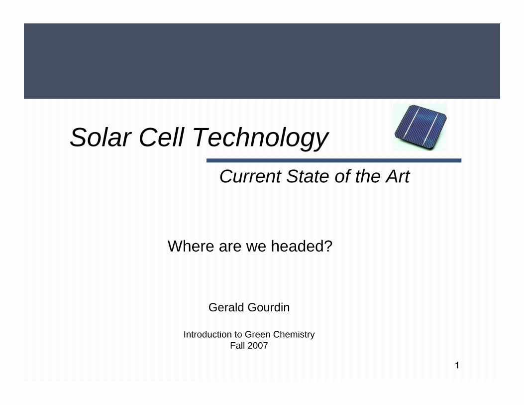
Solar Cell TechnologyCurrent State of the Art
Gerald Gourdin
Introduction to Green ChemistryFall 2007
Where are we headed?
Nov-21-07 2
1839: Photovoltaic effect was first recognized by French physicistAlexandre-Edmond Becquerel.
1883: First solar cell was built by Charles Fritts, who coated thesemiconductor selenium with an extremely thin layer of gold to form thejunctions (1% efficient).
1946: Russell Ohl patented the modern solar cell 1954: Modern age of solar power technology arrives - Bell Laboratories,
experimenting with semiconductors, accidentally found that silicon dopedwith certain impurities was very sensitive to light.
The solar cell or photovoltaic cell fulfills two fundamental functions: Photogeneration of charge carriers (electrons and holes) in a light-absorbing
material Separation of the charge carriers to a conductive contact to transmit electricity
Introduction
Nov-21-07 3
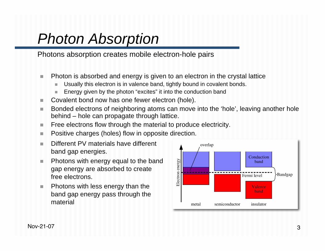
Photon is absorbed and energy is given to an electron in the crystal lattice Usually this electron is in valence band, tightly bound in covalent bonds. Energy given by the photon “excites” it into the conduction band
Covalent bond now has one fewer electron (hole). Bonded electrons of neighboring atoms can move into the ‘hole’, leaving another hole
behind – hole can propagate through lattice. Free electrons flow through the material to produce electricity. Positive charges (holes) flow in opposite direction.
Photon Absorption
Different PV materials have differentband gap energies.
Photons with energy equal to the bandgap energy are absorbed to createfree electrons.
Photons with less energy than theband gap energy pass through thematerial
Photons absorption creates mobile electron-hole pairs
Nov-21-07 4
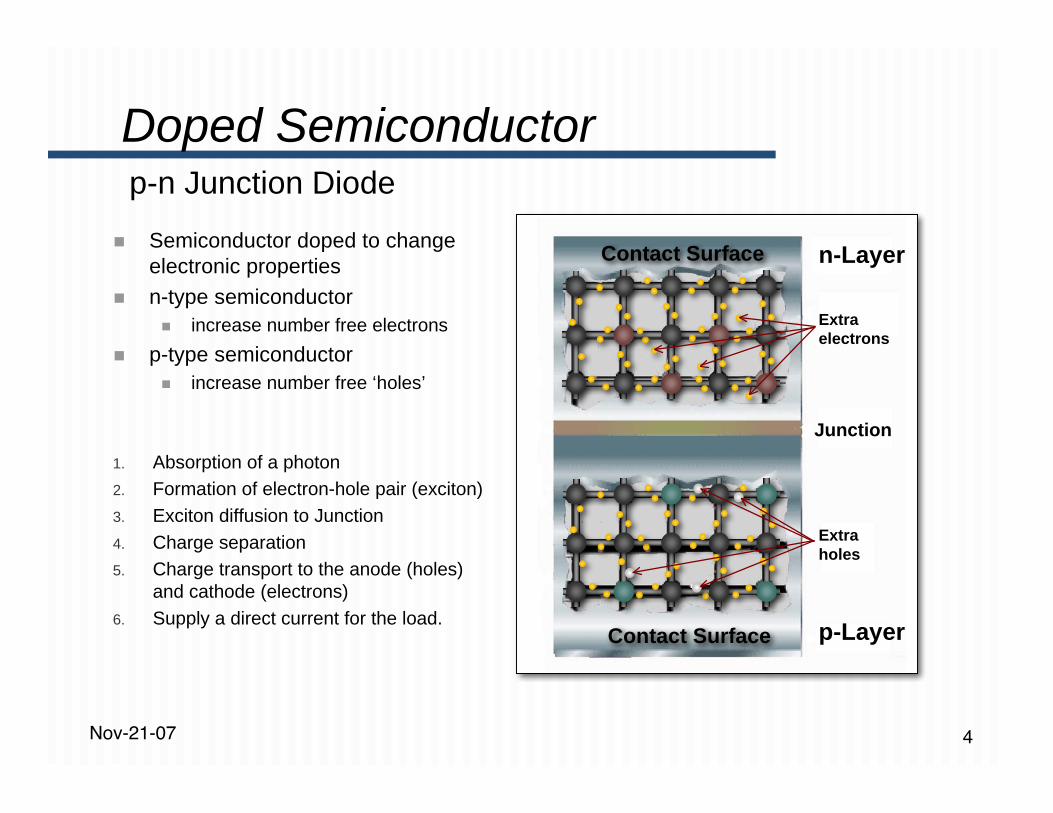
Doped Semiconductor
Extra electrons
Extra holes
n-Layer
p-Layer
Junction
Contact Surface
Contact Surface
1. Absorption of a photon2. Formation of electron-hole pair (exciton)3. Exciton diffusion to Junction4. Charge separation5. Charge transport to the anode (holes)
and cathode (electrons)6. Supply a direct current for the load.
Semiconductor doped to changeelectronic properties
n-type semiconductor increase number free electrons
p-type semiconductor increase number free ‘holes’
p-n Junction Diode
Nov-21-07 5
Electricity Generation
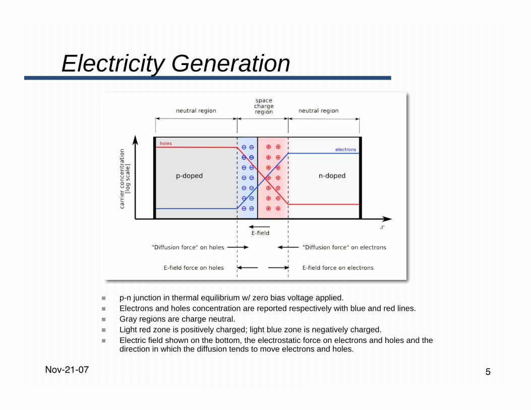
p-n junction in thermal equilibrium w/ zero bias voltage applied. Electrons and holes concentration are reported respectively with blue and red lines. Gray regions are charge neutral. Light red zone is positively charged; light blue zone is negatively charged. Electric field shown on the bottom, the electrostatic force on electrons and holes and the
direction in which the diffusion tends to move electrons and holes.
Nov-21-07 6
Homojunction Device Single material altered so that one side is p-type and the other side
is n-type. p-n junction is located so that the maximum amount of light is
absorbed near it. Heterojunction Device
Junction is formed by contacting two different semiconductor. Top layer - high bandgap selected for its transparency to light. Bottom layer - low bandgap that readily absorbs light.
p-i-n and n-i-p Devices A three-layer sandwich is created, Contains a middle intrinsic layer between n-type layer and p-type
layer. Light generates free electrons and holes in the intrinsic region.
Cell Structures
Nov-21-07 7
First Generation Single crystal silicon wafers (c-Si)
Second Generation Amorphous silicon (a-Si) Polycrystalline silicon (poly-Si) Cadmium telluride (CdTe) Copper indium gallium diselenide (CIGS) alloy
Third Generation Nanocrystal solar cells Photoelectrochemical (PEC) cells
• Gräetzel cells Polymer solar cells Dye sensitized solar cell (DSSC)
Fourth Generation Hybrid - inorganic crystals within a polymer matrix
Overview
Nov-21-07 8
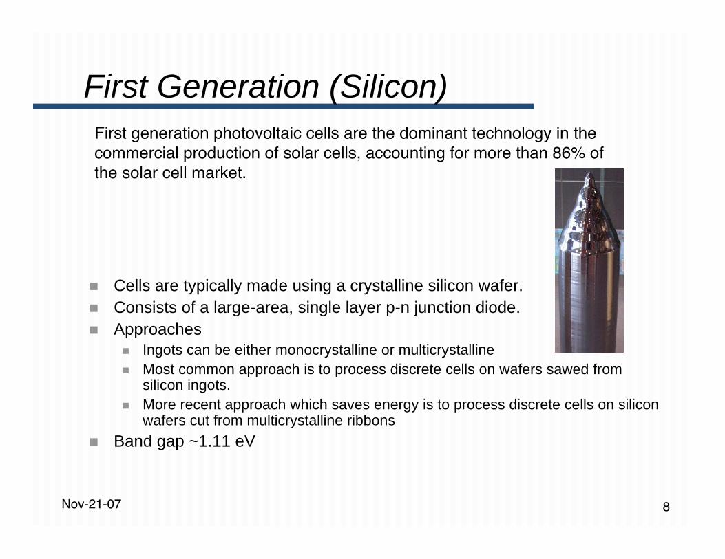
Cells are typically made using a crystalline silicon wafer. Consists of a large-area, single layer p-n junction diode. Approaches
Ingots can be either monocrystalline or multicrystalline Most common approach is to process discrete cells on wafers sawed from
silicon ingots. More recent approach which saves energy is to process discrete cells on silicon
wafers cut from multicrystalline ribbons Band gap ~1.11 eV
First Generation (Silicon)First generation photovoltaic cells are the dominant technology in thecommercial production of solar cells, accounting for more than 86% ofthe solar cell market.
Nov-21-07 9
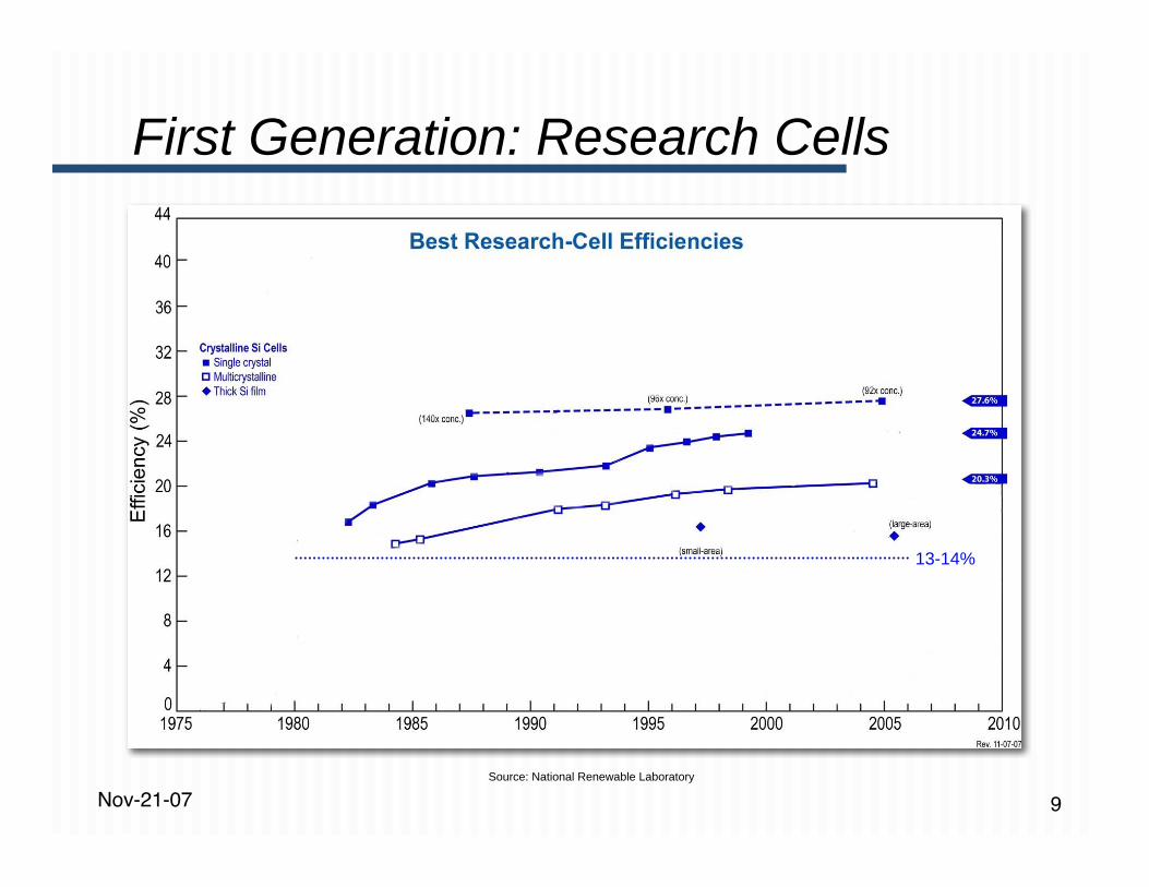
First Generation: Research Cells
13-14%
Source: National Renewable Laboratory
Nov-21-07 10
Advantages Broad spectral absorption range High carrier mobilities
Disadvantages Requires expensive manufacturing technologies Growing and sawing of ingots is a highly energy intensive process Fairly easy for an electron generated in another molecule to hit a hole left
behind in a previous photoexcitation. Much of the energy of higher energy photons, at the blue and violet end of the
spectrum, is wasted as heat
First Generation: Evaluation
Nov-21-07 11
Based on the use of thin-film deposits of semiconductors. Using of thin-films reduces mass of material required for cell design. Contributes greatly to reduced costs for thin film solar cells. Several technologies/semiconductor materials currently under investigation or
in mass production Deposition of thin layers of non-crystalline-silicon materials on inexpensive
substrates using PECVD. Devices initially designed to be high-efficiency, multiple junction photovoltaic
cells.
Second Generation: OverviewThin-film Technology
Nov-21-07 12
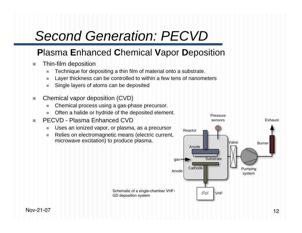
Thin-film deposition Technique for depositing a thin film of material onto a substrate. Layer thickness can be controlled to within a few tens of nanometers Single layers of atoms can be deposited
Second Generation: PECVDPlasma Enhanced Chemical Vapor Deposition
Pumpingsystem
Valve
Pressuresensors
Reactor
Burner
VHF
Exhaust
gas
CathodeAnode
Anode
Substrate
Schematic of a single-chamber VHF-GD deposition system
Chemical vapor deposition (CVD) Chemical process using a gas-phase precursor. Often a halide or hydride of the deposited element.
PECVD - Plasma Enhanced CVD Uses an ionized vapor, or plasma, as a precursor Relies on electromagnetic means (electric current,
microwave excitation) to produce plasma.
Nov-21-07 13
Amorphous silicon cells deposited on stainless-steel ribbon Can be deposited over large areas by plasma-enhanced chemical vapor deposition Can be doped in a fashion similar to c-Si, to form p- or n-type layers Used to produce large-area photovoltaic solar cells Band gap ~ 1.7 eV
Polycrystalline silicon Consists solely of crystalline silicon grains (1mm), separated by grain boundaries Main advantage over amorphous Si: mobility of the charge carriers can be orders of
magnitude larger Material shows greater stability under electric field and light-induced stress. Band gap ~ 1.1 eV
Cadmium telluride (CdTe) cells deposited on glass Crystalline compound formed from cadmium and tellurium with a zinc blende (cubic) crystal
structure (space group F43m) Usually sandwiched with cadmium sulfide (CdS) to form a p-n junction photovoltaic solar
cell. Cheaper than silicon, especially in thin-film solar cell technology - not as efficient Band gap ~ 1.58 eV
Copper indium gallium diselenide (CIGS) alloy cells Deposited on either glass or stainless steel substrates More complex heterojunction model Band gap ~ 1.38 eV
Second Generation: Types
Nov-21-07 14
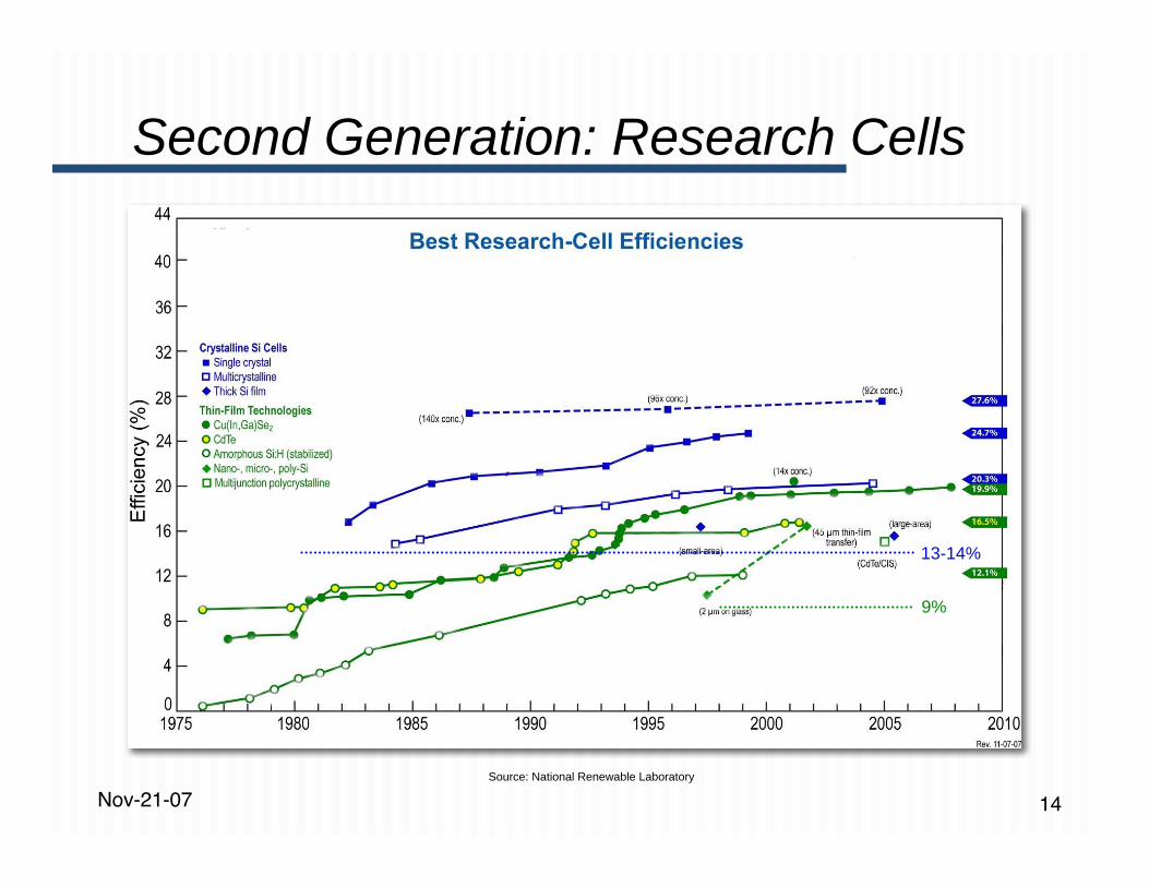
Second Generation: Research Cells
Source: National Renewable Laboratory
9%
13-14%
Nov-21-07 15
Advantages Lower manufacturing costs Lower cost per watt can be achieved Reduced mass Less support is needed when placing panels on rooftops Allows fitting panels on light or flexible materials, even textiles.
Disadvantages Typically, the efficiencies of thin-film solar cells are lower compared
with silicon (wafer-based) solar cells Amorphous silicon is not stable Increased toxicity
Second Generation: Evaluation
Nov-21-07 16
Very different from the previous semiconductor devices Do not rely on a traditional p-n junction to separate
photogenerated charge carriers. Devices include:
Nanocrystal solar cells Photoelectrochemical cells
• Gräetzel Cell Dye-sensitized hybrid solar cells Polymer solar cells
Third Generation: OverviewDifferent Semiconductor Technology
Nov-21-07 17
Third Generation: TypesNanocrystal solar cells
Solar cells based on a silicon substrate with a coating of nanocrystals Silicon substrate has small grains of nanocrystals, or quantum dots
• Lead selenide (PbSe) semiconductor• Cadmium telluride (CdTe) semiconductor
Quantum dot is a semiconductor nanostructure• Confines the motion of conduction band electrons, valence band holes, or
excitons in all three spatial directions. Thin film of nanocrystals is obtained by a process known as “spin-
coating” Excess amount of solution placed onto a substrate then rotated very
quickly Higher current potential for solar cells
Nov-21-07 18
Third Generation: TypesPhotoelectrochemical (PEC) cells
Separate the two functions provided by silicon in a traditional celldesign
Consists of a semiconducting photoanode and a metal cathodeimmersed in an electrolyte. K3 Fe(CN)6/K4 Fe(CN)6
Iodide/Triiodide Fe(CN)6
4-/Fe(CN)63-
Sulphide salt/sulphur Charge separation not solely provided by the semiconductor, but
works in concert with the electrolyte. Gräetzel cells
Dye-sensitized PEC cells Semiconductor solely used for charge separation, Photoelectrons provided from separate photosensitive dye Overall peak power production represents a conversion efficiency of about 11%
Nov-21-07 19
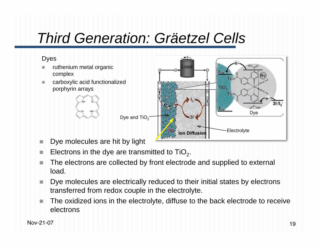
Dye molecules are hit by light Electrons in the dye are transmitted to TiO2. The electrons are collected by front electrode and supplied to external
load. Dye molecules are electrically reduced to their initial states by electrons
transferred from redox couple in the electrolyte. The oxidized ions in the electrolyte, diffuse to the back electrode to receive
electrons
Third Generation: Gräetzel CellsDyes ruthenium metal organic
complex carboxylic acid functionalized
porphyrin arrays
Dye and TiO2
Electrolyte
Load
Nov-21-07 20
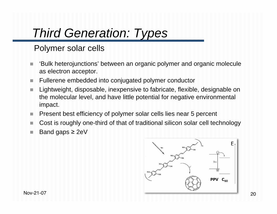
Third Generation: TypesPolymer solar cells
‘Bulk heterojunctions’ between an organic polymer and organic moleculeas electron acceptor.
Fullerene embedded into conjugated polymer conductor Lightweight, disposable, inexpensive to fabricate, flexible, designable on
the molecular level, and have little potential for negative environmentalimpact.
Present best efficiency of polymer solar cells lies near 5 percent Cost is roughly one-third of that of traditional silicon solar cell technology Band gaps ≥ 2eV
Nov-21-07 21
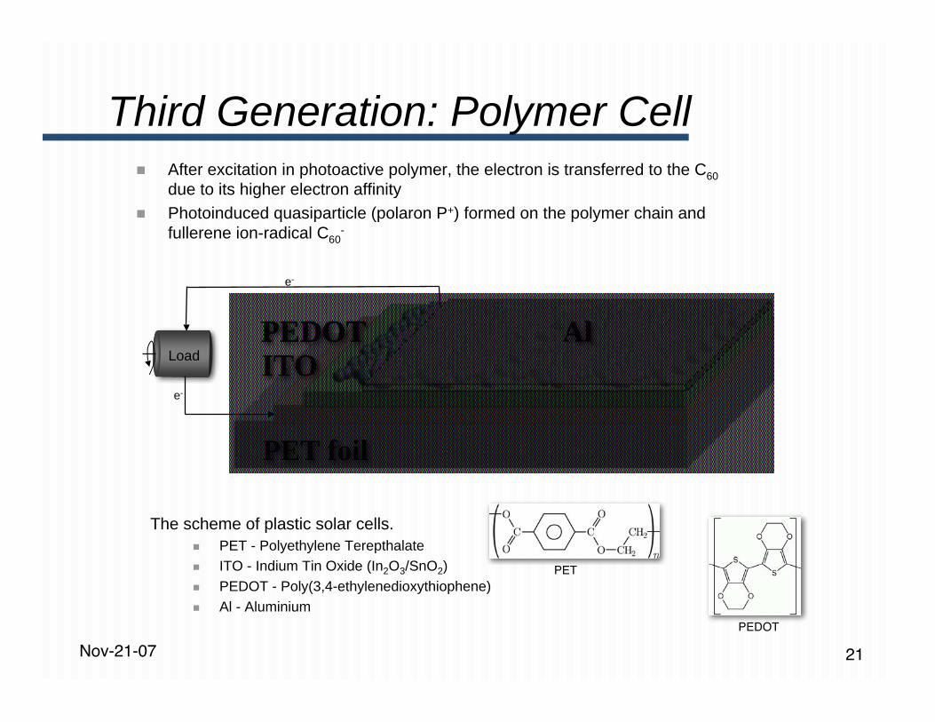
Third Generation: Polymer Cell After excitation in photoactive polymer, the electron is transferred to the C60
due to its higher electron affinity Photoinduced quasiparticle (polaron P+) formed on the polymer chain and
fullerene ion-radical C60-
The scheme of plastic solar cells. PET - Polyethylene Terepthalate ITO - Indium Tin Oxide (In2O3/SnO2) PEDOT - Poly(3,4-ethylenedioxythiophene) Al - Aluminium
PEDOT
PET
PEDOTITO
PET foil
Load
e-
e-
Al
Nov-21-07 22
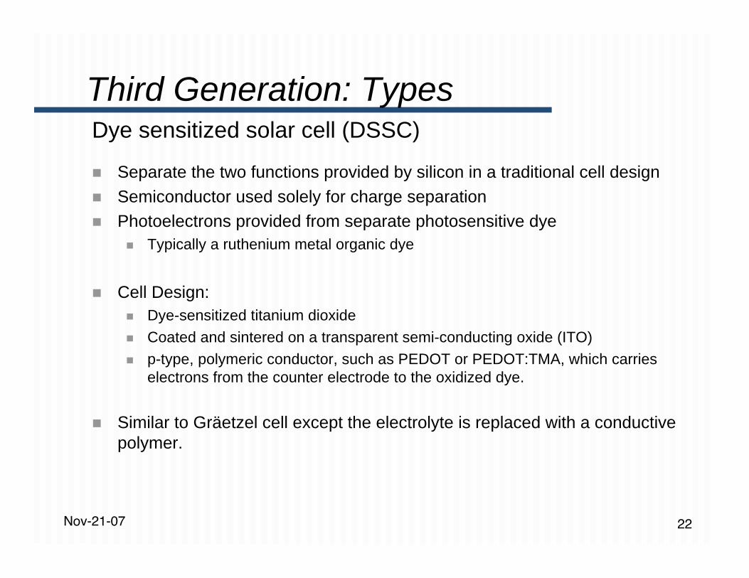
Separate the two functions provided by silicon in a traditional cell design Semiconductor used solely for charge separation Photoelectrons provided from separate photosensitive dye
Typically a ruthenium metal organic dye
Cell Design: Dye-sensitized titanium dioxide Coated and sintered on a transparent semi-conducting oxide (ITO) p-type, polymeric conductor, such as PEDOT or PEDOT:TMA, which carries
electrons from the counter electrode to the oxidized dye.
Similar to Gräetzel cell except the electrolyte is replaced with a conductivepolymer.
Third Generation: TypesDye sensitized solar cell (DSSC)
Nov-21-07 23
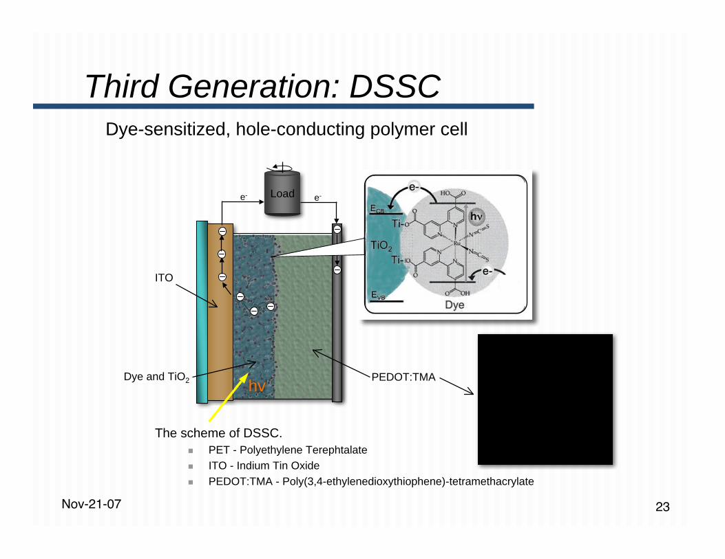
Third Generation: DSSCDye-sensitized, hole-conducting polymer cell
The scheme of DSSC. PET - Polyethylene Terephtalate ITO - Indium Tin Oxide PEDOT:TMA - Poly(3,4-ethylenedioxythiophene)-tetramethacrylate
Load
ITO
Dye and TiO2 PEDOT:TMA
e- e-
hv
Nov-21-07 24
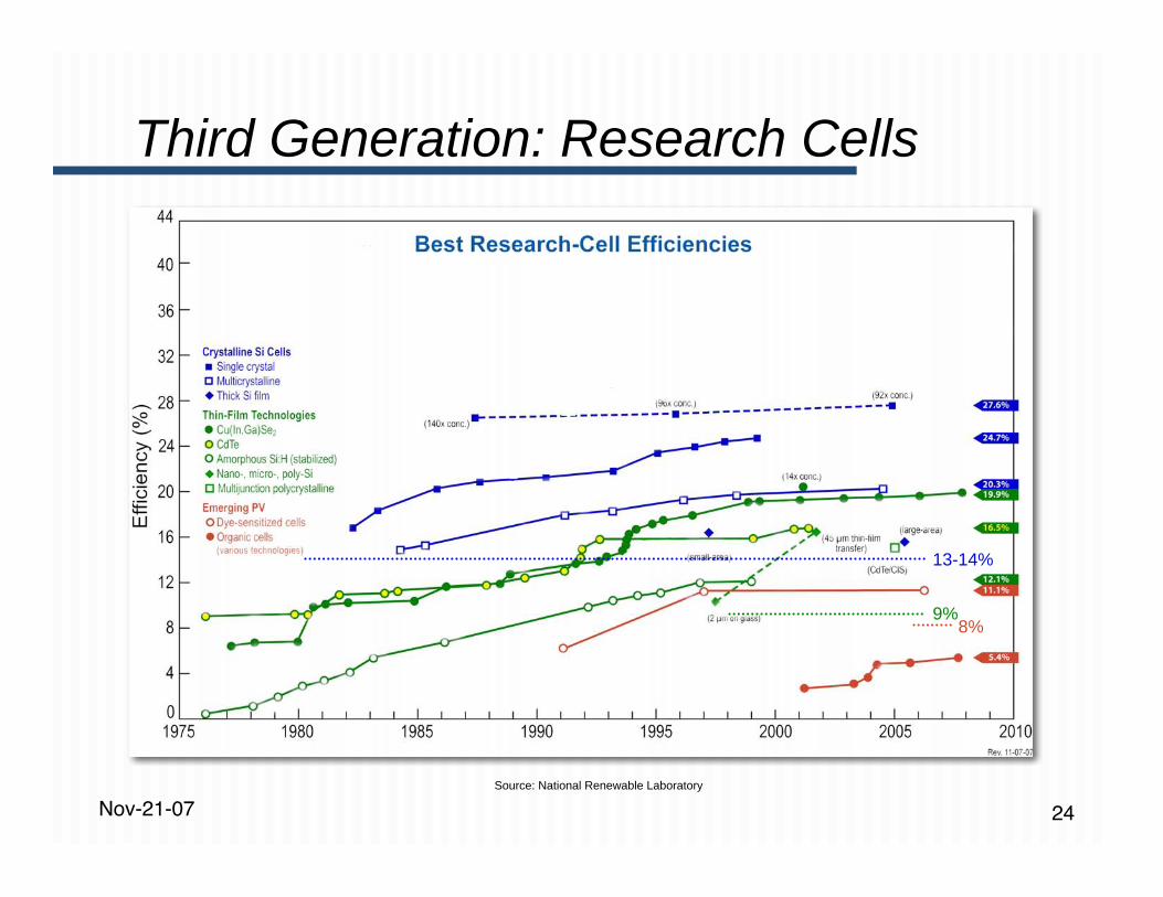
Third Generation: Research Cells
Source: National Renewable Laboratory
8%
13-14%
9%
Nov-21-07 25
Advantages Low-energy, high-throughput processing technologies Polymer cells - solution processable, chemically synthesized Polymer cells - low materials cost Gräetzel cells - attractive replacement for existing technologies in “low
density” applications like rooftop solar collectors Gräetzel cells - Work even in low-light conditions DSSC - potentially rechargeable => upgradeable?
Disadvantages Efficiencies are lower compared with silicon (wafer-based) solar cells Polymer solar cells:
• Degradation effects: efficiency is decreased over time due to environmentaleffects.
• High band gap PEC cells suffer from degradation of the electrodes from the electrolyte
Third Generation: Evaluation
Nov-21-07 26
Hybrid - nanocrystal/polymer cell
Fourth Generation
Composite photovoltaic technologycombining elements of the solid
state and organic PV cells
Nov-21-07 27
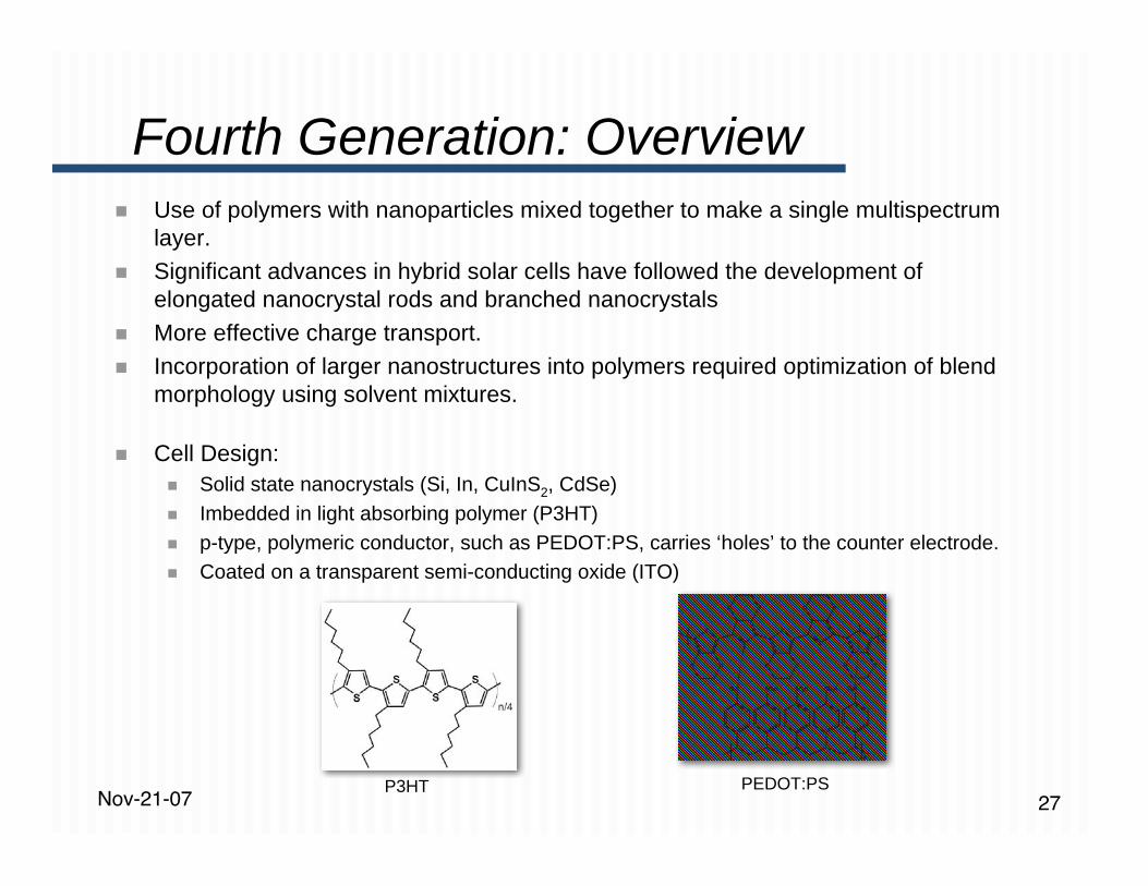
Use of polymers with nanoparticles mixed together to make a single multispectrumlayer.
Significant advances in hybrid solar cells have followed the development ofelongated nanocrystal rods and branched nanocrystals
More effective charge transport. Incorporation of larger nanostructures into polymers required optimization of blend
morphology using solvent mixtures.
Fourth Generation: Overview
P3HT PEDOT:PS
Cell Design: Solid state nanocrystals (Si, In, CuInS2, CdSe) Imbedded in light absorbing polymer (P3HT) p-type, polymeric conductor, such as PEDOT:PS, carries ‘holes’ to the counter electrode. Coated on a transparent semi-conducting oxide (ITO)
Nov-21-07 28
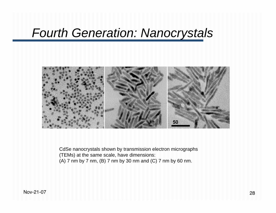
Fourth Generation: Nanocrystals
CdSe nanocrystals shown by transmission electron micrographs(TEMs) at the same scale, have dimensions:(A) 7 nm by 7 nm, (B) 7 nm by 30 nm and (C) 7 nm by 60 nm.
Nov-21-07 29
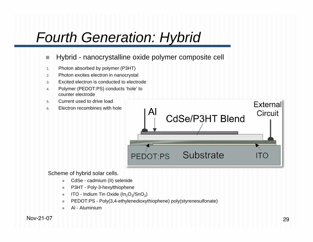
Hybrid - nanocrystalline oxide polymer composite cell
Fourth Generation: Hybrid
Scheme of hybrid solar cells. CdSe - cadmium (II) selenide P3HT - Poly-3-hexylthiophene ITO - Indium Tin Oxide (In2O3/SnO2) PEDOT:PS - Poly(3,4-ethylenedioxythiophene) poly(styrenesulfonate) Al - Aluminium
1. Photon absorbed by polymer (P3HT)2. Photon excites electron in nanocrystal3. Excited electron is conducted to electrode4. Polymer (PEDOT:PS) conducts ‘hole’ to
counter electrode5. Current used to drive load6. Electron recombines with hole
Nov-21-07 30
Thin multi spectrum layers can be stacked to make multispectrum solarcells. Layer that converts different types of light is first Another layer for the light that passes Lastly is an infra-red spectrum layer for the cell Converting some of the heat for an overall solar cell composite More efficient and cheaper Based on polymer solar cell and multi junction technology
Future advances will rely on new nanocrystals, such as cadmium telluridetetrapods. potential to enhance light absorption and further improve charge transport.
Gains can be made by incorporating application-specific organiccomponents, including electroactive surfactants which control the physicaland electronic interactions between nanocrystals and polymer.
Fourth Generation: Future
Nov-21-07 31
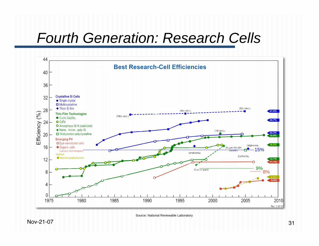
Fourth Generation: Research Cells
15%Hybrid
Nanocrytal/polymer
6.0%
Source: National Renewable Laboratory
9%8%
Nov-21-07 32
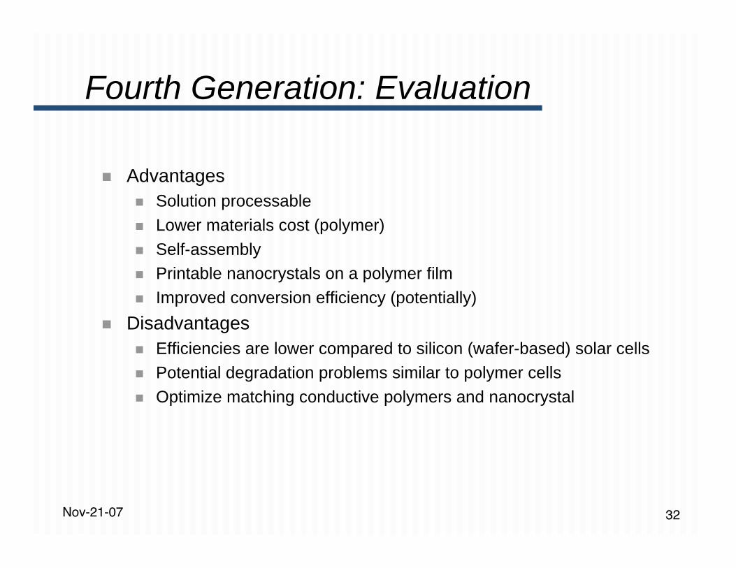
Advantages Solution processable Lower materials cost (polymer) Self-assembly Printable nanocrystals on a polymer film Improved conversion efficiency (potentially)
Disadvantages Efficiencies are lower compared to silicon (wafer-based) solar cells Potential degradation problems similar to polymer cells Optimize matching conductive polymers and nanocrystal
Fourth Generation: Evaluation
Nov-21-07 33
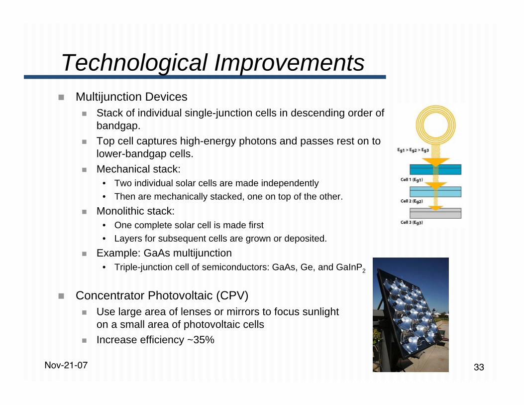
Multijunction Devices Stack of individual single-junction cells in descending order of
bandgap. Top cell captures high-energy photons and passes rest on to
lower-bandgap cells. Mechanical stack:
• Two individual solar cells are made independently• Then are mechanically stacked, one on top of the other.
Monolithic stack:• One complete solar cell is made first• Layers for subsequent cells are grown or deposited.
Example: GaAs multijunction• Triple-junction cell of semiconductors: GaAs, Ge, and GaInP2
Technological Improvements
Concentrator Photovoltaic (CPV) Use large area of lenses or mirrors to focus sunlight
on a small area of photovoltaic cells Increase efficiency ~35%
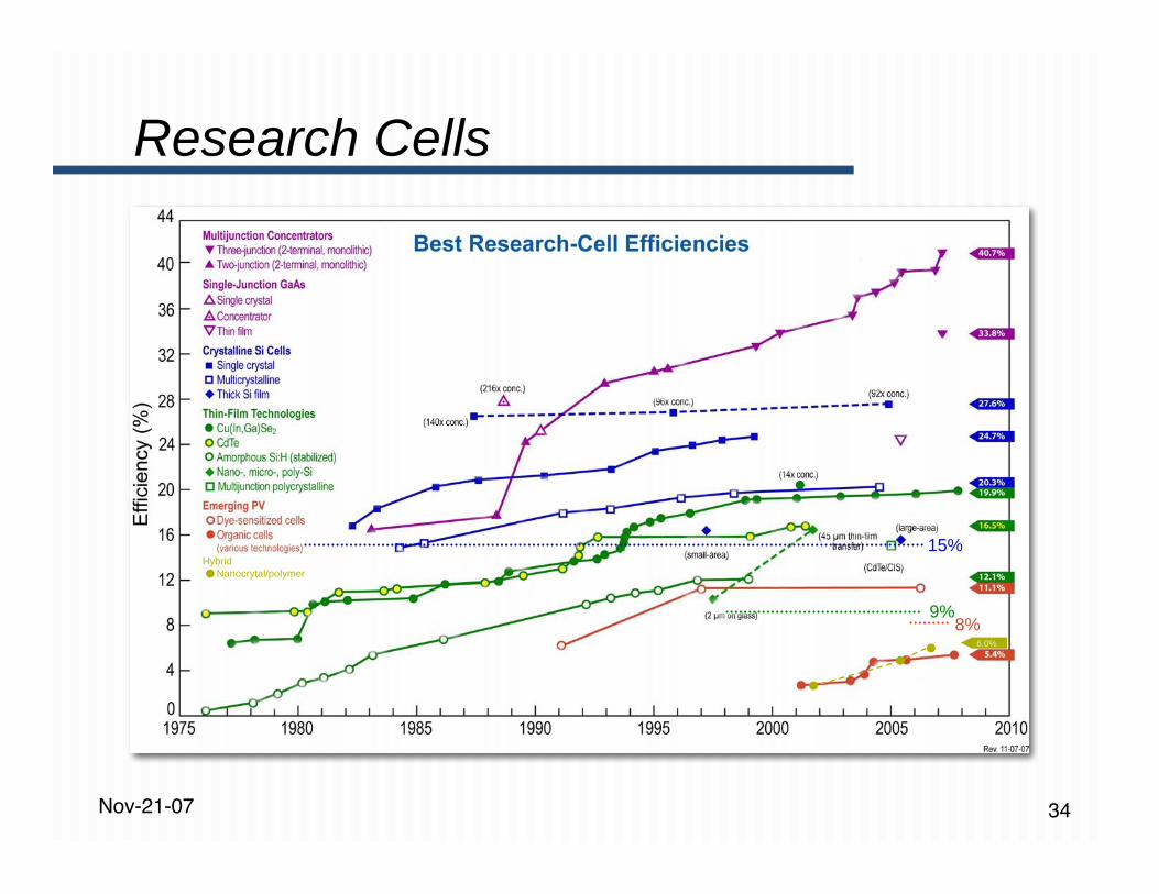
Nov-21-07 34
Research Cells
15%Hybrid
Nanocrytal/polymer
6.0%
9%8%
Nov-21-07 35
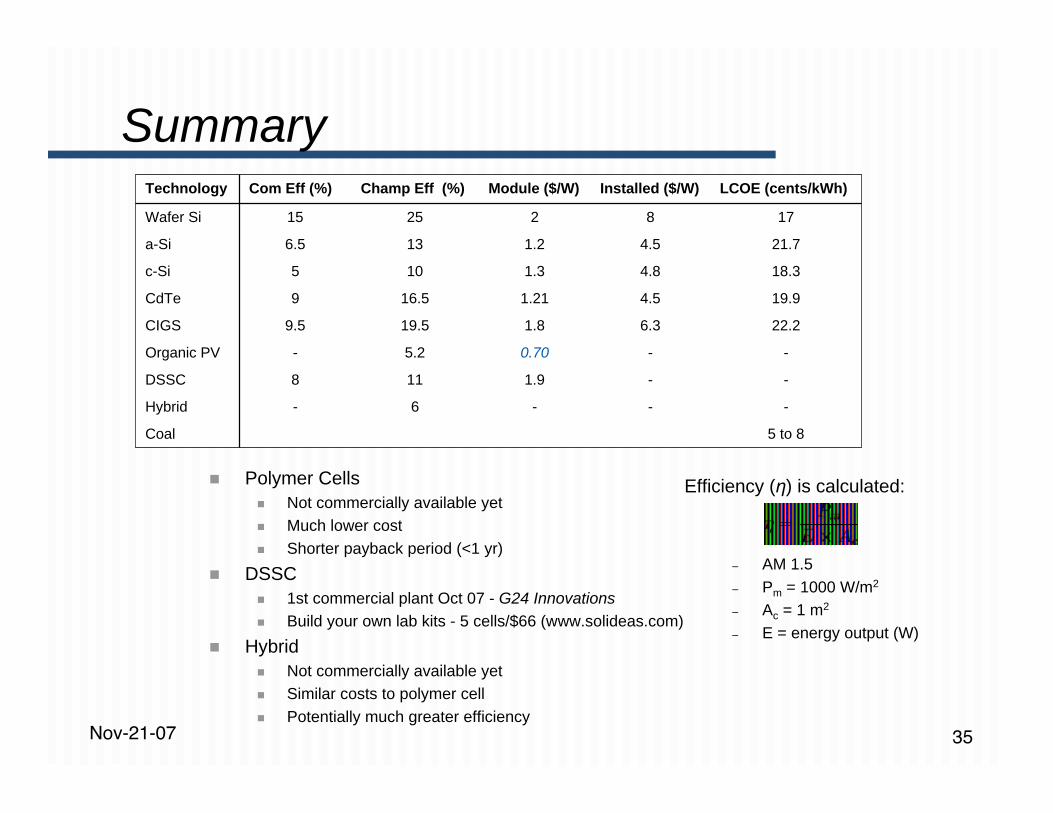
Summary
Polymer Cells Not commercially available yet Much lower cost Shorter payback period (<1 yr)
DSSC 1st commercial plant Oct 07 - G24 Innovations Build your own lab kits - 5 cells/$66 (www.solideas.com)
Hybrid Not commercially available yet Similar costs to polymer cell Potentially much greater efficiency
5 to 8Coal
---6-Hybrid
--1.9118DSSC
--0.705.2-Organic PV
22.26.31.819.59.5CIGS
19.94.51.2116.59CdTe
18.34.81.3105c-Si
21.74.51.2136.5a-Si
17822515Wafer Si
LCOE (cents/kWh)Installed ($/W)Module ($/W)Champ Eff (%)Com Eff (%)Technology
Efficiency (η) is calculated:
– AM 1.5– Pm = 1000 W/m2
– Ac = 1 m2
– E = energy output (W)
Nov-21-07 36
References1. Efficient Titanium Oxide/Conjugated Polymer Photovoltaics for Solar Energy Conversion. Advanced Materials, 2000. 12(22): p. 4.2. Alivisatos, A.P., Hybrid Nanorod-Polymer Solar Cell, in Subcontractor Report, NREL, Editor. 2002, National Renewable Energy
Laboratory: Golden, CO. p. 13.3. Arici, E., N.S. Sariciftci, and D. Meissner, Advanced Functional Materials, 2003. 13(2): p. 7.4. Baumann, A., et al., Photovoltaic Technology Review. 2004, University of California at Berkeley: Berkeley, CA. p. 40.5. C. J. Brabec, N.S.S.J.C.H., Plastic Solar Cells. Advanced Functional Materials, 2001. 11(1): p. 15-26.6. Campbell, W., Harvesting the Sun with Synthetic Porphyrin Dyes Massey University: Auckland, New Zealand.7. Capper, P. and Inspec, Properties of narrow gap cadmium-based compounds. EMIS datareviews series, no. 10. 1994, London:
INSPEC, the Institution of Electrical Engineers.8. Cravino, A. and N.S. Sariciftci, Double-cable polymers for fullerene based organic optoelectronic applications. Journal of Materials
Chemistry, 2002. 12: p. 12.9. Energy, U.S.D.o. Photovoltaics. Solar Energy Technologies Program 2006 04/13/2006 [cited 2007 November 8]; Available from:
http://www1.eere.energy.gov/solar/photovoltaics.html.10. Feitknecht, L.A., Microcrystalline Silicon Solar Cells In The N-I-P Configuration: Optimisations On Light Scattering Back-Reflectors, in
Institut de Microtechnique. 2003, Universit ́e de Neuchˆatel.11. Gasman, L. Thin-film and Organic PV on the Rise. 2006 2006 [cited 2007 11/9/07]; Available from:
http://www.renewableenergyaccess.com/rea/news/story?id=44634.12. Gebeyehua, D., et al., Synthetic Metals 2001. 125(3): p. 8.13. Ginley, D., National Solar Technology Roadmap: Organic PV in National Solar Technology Roadmap. 2007, National Renewable
Energy Laboratory: Golden, CO. p. 5.14. Gratzel, M., J. of Sol-Gel Sci. and Tech., 2001. 22: p. 7.15. Halme, J., Dye-sensitized nanostructured and organic photovoltaic cells: technical review and preliminary tests, in Department of
Engineering Physics and Mathematics. 2002, Helsinki University of Technology. p. 115.16. Hoppe, H. and N.S. Sariciftci, Organic solar cells: An overview. Journal of Materials Research, 2004. 19(7): p. 22.17. Hoppe, H. and N. Serdar Sariciftci, Organic solar cells: An overview J. Mater. Res, 2004. 19(7): p. 1924-1945.18. Keyes, B., National Solar Technology Roadmap: Film-Silicon PV in National Solar Technology Roadmap. 2007, National Renewable
Energy Laboratory: Golden, CO. p. 7.
Nov-21-07 37
References (cont)19. Laboratory, N.R.E. [cited; Available from: www.nrel.gov.20. Licht, S., A Description of Energy Conversion in Photoelectrochemical Solar Cells. Nature, 1987. 300(12): p. 148-151.21. Licht, S. and D. Peramunage, Efficient Photoelectrochemical Solar Cells from Electrolyte Modification. Nature, 1990. 345(24): p. 330-
33.22. Lorenzo, E., Solar electricity engineering of photovoltaic systems. 1994, Sevilla, Spain: PROGENSA.23. Luque, A. and S. Hegedus, Handbook of photovoltaic science and engineering. 2003, Hoboken, NJ: Wiley.24. Matson, R., National Solar Technology Roadmap: Sensitized Solar Cells, in National Solar Technology Roadmap. 2007, National
Renewable Energy Laboratory: Golden, CO. p. 6.25. Mozer, A.J. and N.S. Sariciftci, Conjugated polymer photovoltaic devices and materials. Comptes Rendus Chimie 2006. 9(5-6): p. 568-
577.26. Noufi, R. and K. Zweibel, High Efficiency CdTe and CIGS Thin Film Solar Cells: Highlights of the Technologies Challenges, in 006
IEEE 4th World Conference on Photovoltaic Energy Conversion (WCPEC-4). 2006: Waikoloa, Hawaii.27. Sopori, B., National Solar Technology Roadmap: Wafer-Silicon PV in National Solar Technology Roadmap. 2007, National Renewable
Energy Laboratory: Golden, CO. p. 6.28. Tennakone, K., et al., An efficient dye-sensitized photoelectrochemical solar cell made from oxides of tin and zinc. Chemical
Communications, 1998: p. 2.29. Tongpoola, R., et al., Dye-SensitizedSolarCell (DSSC), National Metal and Materials Technology Center (MTEC): Klongluang,
Pathumthani, 12120, Thailand. p. 1.30. Ullal, H., National Solar Technology Roadmap: CdTe PV in National Solar Technology Roadmap. 2007, National Renewable Energy
Laboratory: Golden, CO. p. 6.31. von Roedern, B., National Solar Technology Roadmap: CIGS PV in National Solar Technology Roadmap. 2007, National Renewable
Energy Laboratory: Golden, CO. p. 6.32. Watt, A.R., et al., Lead sulfide nanocrystal: conducting polymer solar cells. J. Phys. D: Appl. Phys, 2005. 38: p. 2006-2012.33. Wikipedia. Solar Cell. 2007 6 November 2007 [cited 2007 November 8]; Available from: http://en.wikipedia.org/wiki/Solar_cell.34. Wormser, P. and R. Gaudiana, Polymer Photovoltaics –Challenges and Opportunities, in NCPV and Solar Program Review Meeting
2003. 2003, NREL/CD.

Nov-21-07 38
The End
Thank you!


![Green Chem- Scrap Tires[1]alpha.chem.umb.edu/chemistry/ch471/documents/GreenChem-Scrap… · Disposal Scrap tires represents one of the most difficult recycling problems ever encountered](https://img.pdfslide.net/doc/110x75/5ae616597f8b9a29048d1317/green-chem-scrap-tires1alphachemumbeduchemistrych471documentsgreenchem-scrapdisposal.jpg)