Embed Size (px)
Citation preview


A GSM Band Low-Power LNA
1. LNA Schematic
Fig1.1 Schematic of the Designed LNA

2. Design Summary
Specification Required Simulation Results
Peak S21 (Gain) > 10dB >11 dB
3dB Bandwidth > 200MHz (<300MHz) 574 M
Center Frequency 900MHz 893.5 MHz
Noise Figure < 1.7dB (800-1000MHz) 1.275dB (800MHz)
1.566dB (1000MHz)
S11 < -10dB (800-1000MHz) -10.45dB (800MHz)
-25.56dB (917.6MHz)
-14.26dB (1000MHz)
P1dB >-30dBm (input referred) -3.68dBm
IIP3 >-15dBm (input referred) 7.586dBm
Power Consumption <4mW (total) 3.846mW

3. Simulation Results
Fig1.2 Simulation Result for S21
Fig1.3 Simulation Result for S11

Fig1.4 Simulation Result for Noise Figure
Fig1.5 Simulation Result for P1dB

Fig1.6 Simulation Result for IIP3 (Start point = -10dBm)
Fig1.6 Simulation Result for IIP3 (Start point = -28dBm)

- 1 -
CAD II: Low-oise Amplifier Design
I. Device parameter summary
Inductors
Locations Value Outer diameter # of Turns
gate inductance 16.407 nH 1.64 mm 2
source degen. 2.498 nH 410 um 2
load inductance 171.22 nH 10 mm 2
Capacitor (for CGS compensation)
Location Value X dimension Y dimension
Cgs compensation 16.407 nH 1.64 mm 2
MOSFET
Location Width Length #r of fingers
Input 200 um 0.14 um 1
II. Simulation Results
Parameters Result
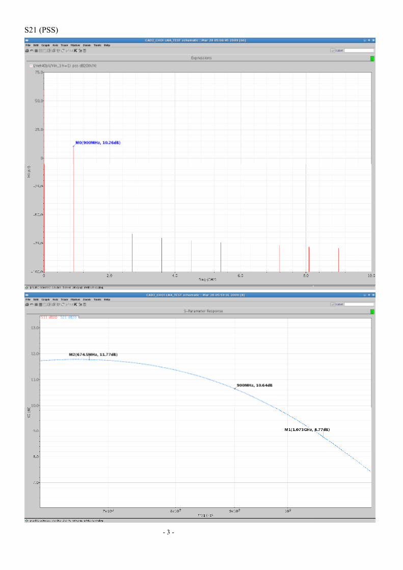
Peak S21 (Gain) 10. 26 dB
3 dB BW 797 MHz
Center Freq. 674.5 MHz
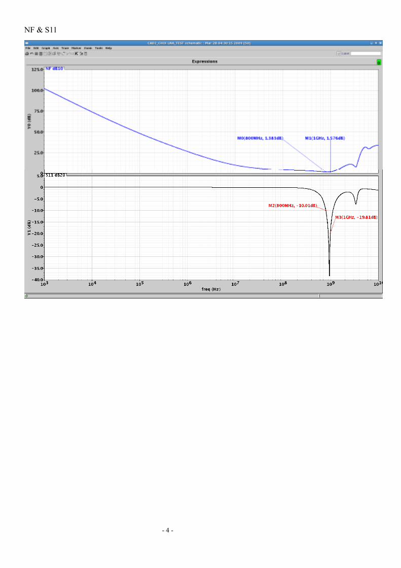
S11 -10.01 dB
Noise Figure < 1.576 dB
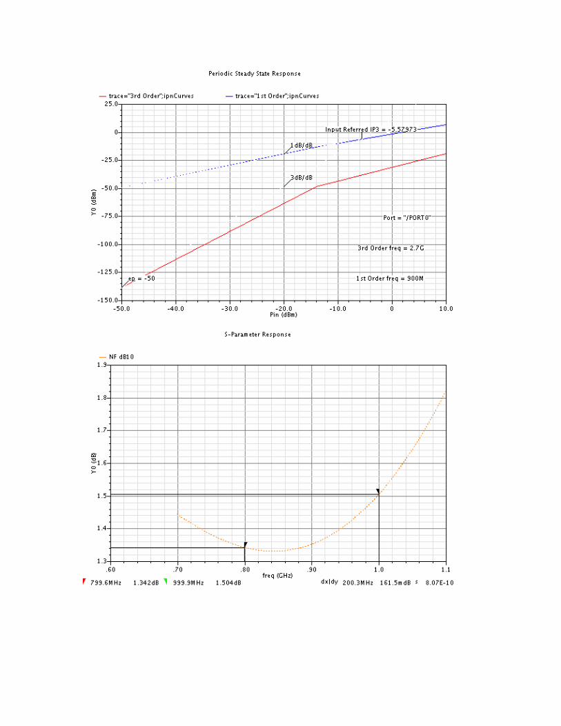
P1 dB - 12.79 dBm
IIP3 - 7.52 dB
Power Consumption 3.66 mW

- 2 -
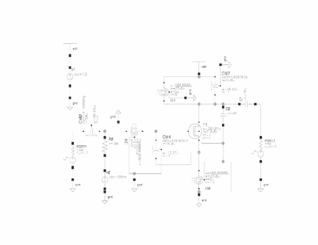
Schematic
- 3 -
S21 (PSS)
- 4 -
NF & S11

- 5 -
P1dB

- 6 -
IIP3

Figure 1. NF, S11, S21

Figure2. 1dB Compression point.

Figure 3. 3dB Compression point.

Specification Desired Achieved
Peak S21 Gain >10dB 15dB
3dB Bandwidth 200MHz ‐ 300MHz 500MHz to 1.028GHz
Center Frequency 900MHz
763MHz (for peak Gain) ~900MHz (for
NF) Noise Figure <1.7dB 1.25dB ‐ 1.31dB S11 <‐10dB ‐10.2dB P1dB >‐30dB ‐8.04dB IIP3 >‐15dB ‐1.113dB Power Consumption < 4mW 3.8mW
Table 1. Desired vs. Achieved values

EECS 522 CAD2 1. Schematic of the LNA
c
Vbias
c
Output port
= 325 mV
Input port
W/L = 510µm
320nm
W/L = 510µm
320nm
1µF
50fF
17pF60µm x 60.59µm
10KΩ
12pF50µm x 49.99µm
Vdd = 1.2V
946 pHturns = 1
Dimention = 390µm
1.63 nHturns = 1.5
Dimention = 380µm
20.15 nHturns = 2.5
Dimention = 1340µm

2. Summary Table
Specification LNA Design
Peak S21 > 10 dB 12.4 dB
3dB Bandwidth 200 MHz ~ 300 MHz 242 MHz
Center Frequency 900 MHz 880 MHz
Noise Figure < 1.7 dB from 800 MHz to 1 GHz < 1.69 dB (in band)
S11 < ‐10 dB from 800 MHz to 1 GHz < ‐10.03 dB (in band)
P1dB > ‐30 dBm ‐1.57 dBm
IIP3 > ‐15 dBm 8.15 dBm
Power < 4 mW 3.924 mW
Path: /afs/umich.edu/user/k/k/kkhuang/eecs522/CAD/CAD_LNA
3. Plots of S11 S21 P1dB IIP3 and Noise Figure


EECS522 CAD 2Submitted March 28, 2009
TABLE OF MEASURED VALUES AND SPECIFICATIONS
Specification Required This LNA
Peak S21 (Gain) > 10 dB 13.99 dB3dB Bandwidth 200 MHz < BW <300 MHz 299.5 MHz
Center Frequency 900 MHz 895.7 MHzNoise Figure < 1.7 dB between 800 MHz and 1 GHz 1.682 dB max
S11 < -10 dB between 800 MHz and 1 GHz -10.32 dB maxP1dB > -30 dBm (input feferred) -7.15861 dBIIP3 > -15 dBm (input referred) 14 dBm
Power Consumption < 4mW (including bias circuits) 3.972 mW*
* 3.31 mA is drawn from the 1.2 V supply by the transistors, the bias resistor contribution is negligible (~5 pW)
Attached (in order):– Illustration of the schematic– Plots
– S11– S21– P1dB– IIP3– Noise Figure


Specification Goal Simulation Results S21(Gain) >10 dB >13 dB
3db Bandwidth 200 MHz < BW <300 MHz 283 MHz
Center Frequency 900 MHz 900 MHz
Noise Figure <1.7 dB between 800MHz & 1GHz
<1.6 dB between 800MHz & 1GHz
S11 <-10 dB between 800 MHz & 1 GHz
<-10 dB between 800 MHz & 1 GHz
P1dB >-30 dBm input referred -8.3 dBm
IIP3 >-15 dBm input referred -4.4 dBm
Power Consumption <4mW 3.87 mW


Schematic
The bias voltage was set to 0.370 VDC.

Summary Peak S21 3dB BW IIP3 1 dB
Compression Power
Design 13.548 dB 225.4 MHz -5.58 -5.75 dBm 3.953 mW Goal > 10 dB 200 MHz
< BW < 300 MHz
> -15 dBm >-30 dBm < 4 mW
Frequency S21 NF S11 800 MHz 12.211 dB 1.3421 dB -10.982 dB 900 MHz 13.518 dB 1.3518 dB -29.761 dB 1 GHz 12.785 dB 1.5043 dB -11.326 dB Plots


CAD #2 Dan Prince
EECS 522
3/27/09
Table 1 - Specification List
Specification Target Value Actual Value
Lower Corner
Actual Value
900MHz
Actual Value
Upper Corner
Peak S21 > 10dB 13.05 dB 13.66 dB 12.79 dB
3dB BW 200MHz < BW < 300MHz N/A 450 MHz N/A
Center Frequency 900MHz N/A 900 MHz N/A
Noise Figure <1.7dB between 800MHz
and 1GHz
1.343 dB 1.343 dB 1.675 dB
S11 <10dB between 800MHz
and 1GHz
-10.62 dB -22.32 dB -10.14 dB
P1dB > -30dBm N/A -4.63 dBm N/A
IIP3 > -15dBm N/A -4.23 dBm N/A
Power Consumption < 4mW N/A 3.994 mW N/A
Table 2 - Component List
Component Parameters
Capacitance Length Width
CM2 Capacitor 830.6277fF 8.5um 11.05um
CM1 Capacitor 4.999709fF 8.5um 81.71um
Inductance Outer Dimension n turns
I3 Inductor 28.043nH 400um 8
I4 Inductor 1.609nH 150um 3
I5 Inductor 4.673nH 300um 3
Width Length # fingers
T1 NFET 200um 150nm 8
T6 NFET 200um 150nm 8
CAD #2 Dan Prince
EECS 522
3/27/09

CAD #2 Dan Prince
EECS 522
3/27/09

CAD #2 Dan Prince
EECS 522
3/27/09


figure 4 designed circuit

figure 5 s parameter analysis results ( s11)

figure 6 s parameter analysis results ( s21)

figure 7 s parameter analysis results (Noise Factor)

figure 6 1 dB compression point

figure 7 IIP3 Point (it is -3.9 dBm, red line is 3th harmonic blue is fundamental)

3‐27‐09
EECS 522 CAD 2
EECS 522 CAD Assignment #2
Figure 1. Schematic of 900 MHz LNA Including Given Components
Device Values and Sizes: Given Devices: RS = 50 Ω Rbias = 10 k Ω CC = 12 pF CL = 50 fF VDD = 1.2 V Vbias = 397 mV

Inductors:
Inductance Outer
Diameter Metal Width
Number of Turns
LG 23.075 nH 470 µm 11 µm 7.5 LS 1.025 nH 400 µm 10 µm 1
LD 2.266 nH 290 µm 15 µm 2.5 Capacitors:
Capacitance X‐Dimension Y‐Dimension CX 709.6945 fF 50 µm 6.75 µm
CD 11.60083 pF 200 µm 28.12 µm Transistors:
Width of Single
Finger Width of All Fingers Length
Number of Fingers
M1 15.21 µm 380.25 µm 160 nm 25
M2 15.21 µm 380.25 µm 160 nm 25 Summary Table:

Plots:
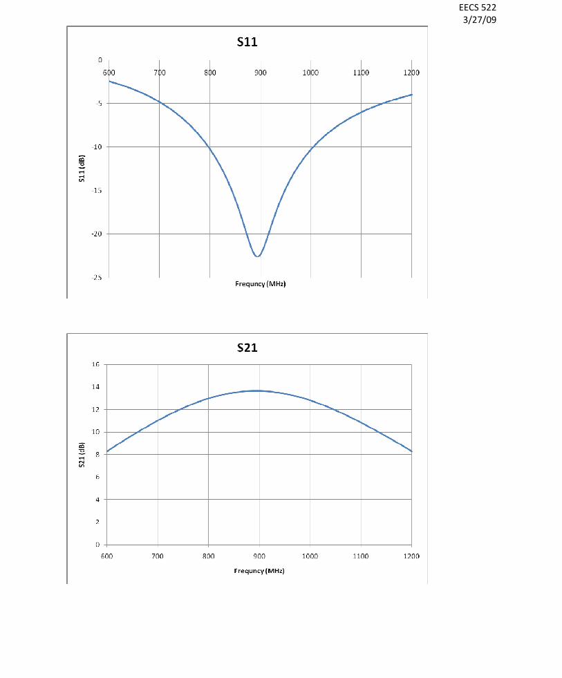
Figure 2. Plot of S11
Figure 3. Plot of S21

Figure 4. Plot of P1dB
Figure 5. Plot of IIP3

Figure 6. Plot of Noise Figure


![N VG [ U{FZJ VG]EJLV[ KLV[P - Gujarat · N VG [ U{FZJ VG]EJLV[ KLV[P - Gujarat ... s], - - - - 5](https://img.pdfslide.net/doc/110x75/5e13200df3ca9032df67634a/n-vg-ufzj-vgejlv-klvp-gujarat-n-vg-ufzj-vgejlv-klvp-gujarat-.jpg)