Embed Size (px)
Citation preview

This content has been downloaded from IOPscience. Please scroll down to see the full text.
Download details:
IP Address: 136.152.142.36
This content was downloaded on 15/02/2017 at 22:19
Please note that terms and conditions apply.
Solution-processed image sensors on flexible substrates
View the table of contents for this issue, or go to the journal homepage for more
2016 Flex. Print. Electron. 1 043001
(http://iopscience.iop.org/2058-8585/1/4/043001)
Home Search Collections Journals About Contact us My IOPscience
You may also be interested in:
Challenges of small-pixel infrared detectors: a review
A Rogalski, P Martyniuk and M Kopytko
Copper(I) thiocyanate (CuSCN) as a hole-transport material for large-area opto/electronics
Nilushi Wijeyasinghe and Thomas D Anthopoulos
HgCdTe infrared detector material
A Rogalski
Semiconductor ultraviolet photodetectors based on ZnO and MgxZn1xO
Yaonan Hou, Zengxia Mei and Xiaolong Du
Electronic and optoelectronic materials and devices inspired by nature
P Meredith, C J Bettinger, M Irimia-Vladu et al.
Quantum dot optoelectronic devices: lasers, photodetectors and solar cells
Jiang Wu, Siming Chen, Alwyn Seeds et al.
Photonics and optoelectronics of two-dimensional materials beyond graphene
Joice Sophia Ponraj, Zai-Quan Xu, Sathish Chander Dhanabalan et al.
One dimensional Si/Ge nanowires and their heterostructures for multifunctional applications—a
review
Samit K Ray, Ajit K Katiyar and Arup K Raychaudhuri
Polymer–fullerene bulk heterojunction solar cells
Carsten Deibel and Vladimir Dyakonov
Flex. Print. Electron 1 (2016) 043001 doi:10.1088/2058-8585/1/4/043001
TOPICAL REVIEW
Solution-processed image sensors on flexible substrates
Adrien Pierre1 andAnaClaudiaAriasDepartment of Electrical Engineering andComputer Sciences, University of California, Berkeley, Berkeley, CA 94720,USA1 Author towhomany correspondence should be addressed.
E-mail: [email protected]
Keywords: image sensor, organic, photodiode, phototransistor, flexible, printing, solution-processed
AbstractImage sensors are ubiquitous and used in awide variety of applications ranging from consumerproducts to healthcare and industrial applications. The signal-to-noise ratio (SNR) of an imageincreases with larger pixels, which is costly to scale using silicon andwafer-basedmicrofabrication. Onthe other hand, the performance of solution-processed photodetectors and transistors is advancingconsiderably. The printability of these devices on plastic substrates can enable low-cost scaling oflarge-pixel, high SNR image sensors. In addition, theflexibility of the substrates can enable newimaging systems never possible with the rigidity of conventional sensors. In this workwe review theprogressmade towards solution-processed image sensors on flexible substrates. The fundamentaloperation of image sensors using intra-pixel charge integration isfirst explained to introduce thefigures ofmerit for these systems. The physics, figures ofmerit, and state of the art for solution-processed photodiodes and phototransistors is also overviewed. A literature survey is done onsolution-processed passive and active pixel image sensors with emphasis on active-switching for intra-pixel charge integration. Finally, optics compliant with large area andflexible image sensors arereviewed.
1. Introduction
The mass production of image sensors has revolutio-nized the landscape of media broadcasting, surveil-lance, medicine andmany other domains that benefitsfrom captured photographs or videos. This prolifera-tion of image sensors was strongly attributed toMoore’s law, which continuously scaled down transis-tor size in order to increase the device speed but also todecrease the cost per device since more chips andsensors can be packed into one silicon wafer [1, 2].Consequently, for a fixed number of pixels, the costper image sensor decreased by shrinking the pixeldimensions. Furthermore, advances in silicon micro-fabrication technology enabled high performancetransistors to be embedded in each pixel for amplifyingthe photo-accumulated charge. Despite suchadvances, the signal-to-noise ratio (SNR) and dynamicrange (range of photographable light intensities) ofimage sensors with small pixels becomes limited by thequantized nature of light, known as shot noise [3–5].For this reason high performance image sensors havelarger pixels on the order of tens of micrometers in
dimension, while inexpensive and low performanceimagers have pixel dimensions of approximately 1micrometer [3, 4].
It becomes clear that alternatives to silicon wafer-based microfabrication technology are necessary inorder to circumvent the trade-off between pixel size,which is correlated to performance, and cost. Proces-sing techniques that scale favorably with area, such asprinting, can leverage the superior performance of largepixels without increasing the cost. This is because sen-sor size is no longer limited by the area of a siliconwafer, but can be deposited on inexpensive substrates ina continuous roll-to-roll fashion [6, 7]. The most pre-valent of these materials are solution processableorganic compounds, Perovskites and inorganic nano-materials that have highly tunable absorption spec-trums and high absorption coefficients. This is in strongcontrast to the poor absorption coefficient of silicon,which can only be improved upon in conventionalmicrofabrication with the costly epitaxial deposition ofa handful of materials. Furthermore, the ability todeposit functional materials on a variety of flexible anddeformable substrates can make conformal substrates
RECEIVED
18August 2016
ACCEPTED FOR PUBLICATION
20 September 2016
PUBLISHED
9November 2016
© 2016 IOPPublishing Ltd

which not only relax the requirements of the optics tofocus the light, but also enable newmethods of imagingnever possible with planar sensors [8]. A significantamount of emerging literature can be found on solutionprocessable and flexible image sensors with a wide vari-ety of pixel architectures and operational modes. Assuch, it is important to assess the progress and short-comings of this young field while emphasizing thefigures of merit and most optimal way of designingdevices and systems for image sensing.
2. Fundamental operation principles ofimage sensors
Image sensors are complex systems, composed ofmultiple types of devices such as the photodetectors andtransistors in each pixel of the array along with thedrivers and readout circuitry outside the sensor area.While printing large area and flexible image sensors canenable features and performance never possible withplanar and compact versions, it is important assess newsystems by the same figures of merit used in conven-tional image sensors [3, 4]. Figure 1(a) shows the path ofthe light-induced photocurrent signal from the photo-detector element in the pixel (black square), throughthe pixel circuitry (red square) andfinally to the readoutcircuitry at the exterior of the array. Almost allcommercialized image sensors employ an active-switching pixel architecture to enable charge integra-tion [1, 3, 4] as illustrated in step 1 offigure 1(a). Placinga capacitor in series with the photocurrent source of thedetector enables integration of the signal during for aperiod of time. The integration period ends when asignal from the row line triggers the pixel to dischargethe photogenerated charge onto the column line in step2. A passive pixel architecture directly transfers thephotogenerated charge from the pixel to the column,giving it a charge output gain (labeled G in figure 1(a))of unity. Conversely, an active pixel utilizes multipletransistors to amplify the charge output from the pixelonto the column. Step 3 shows the injected charge isfinally fed into the readout circuit at the base of thecolumn to translate the photogenerated signal into avoltage so that it can be read by analog to digitalconverters. This conversion can be done by reading thevoltage drop across a passive load such as a resistor, theoutput of a charge amplifier or the output of atransimpedance amplifier. The base of each column isequipped with readout circuitry in order to parallelizethe readout process as each row is scanned.
The intra-pixel charge integration enabled byactive-switching in step 1 offers a far higher SNR com-pared to looking at the instantaneous photocurrent ofeach pixel as it is scanned. Reading out the instanta-neous photocurrent from each pixel means that thesampling period from each row must be very short inorder to scan the array at an appreciable frame rate. On
the other hand, figure 1(b) shows photocurrent can beintegrated in the pixel while it is switched off duringmost of the frame period (step 1), then dischargedquickly into the column line for reading out the charge(steps 2 and 3). This simultaneous charge integration(image capturing) and discharging of pixels in an arrayis known as rolling shutter operation. Global shutteroperation on the other hand, as illustrated infigure 1(c), simultaneously integrates charge over thewhole array for a period of time to prevent motionartifacts, holds the charge, then discharges it row byrow. Intra-pixel integration using either of theseschemes allows for the strength of the signal toincrease linearly with time. The noise of the photo-current and dark current of a photodetector must alsobe taken into account, which can be modeled as a sta-tistical Poisson process [3, 5]. The noise of a currentsource is the standard deviation of integrated chargeduring a certain time period. In a Poisson process, thestandard deviation and noise is the square root of theintegrated charge, which is known as the shot noise ofa device. Equation (1) illustrates the most importantfigure of merit for measuring sensitivity of an imagesensor, signal to noise ratio (SNR) as a function ofphotocurrent (IPhoto), dark current (IDark), fixed read-out noise (NRO) from steps 2 and 3 and integrationtime (T, which is very close to the frame period). Thephotocurrent and dark current are then decomposedinto photocurrent density ( JPhoto) and dark currentdensity ( JDark) multiplied by the photosensitive areaper pixel (A) to demonstrate how scaling photoactivearea affects SNR. The equation is further simplified toshow the case for short and long integration timeswhere the shot noise from the photodetector elementis negligible and significantly larger compared to thereadout noise, respectively. In both cases it is desirableto have a lower dark current density, larger photo-active area and longer integration time for a fixed lightflux (i.e. constant JPhoto). The benefit of large area pix-els is especially predominant for shorter integrationtimes because small pixels easily result in readoutnoise dominating over shot noise [3]. As a result of thistrend it is important to create image sensors with largepixel photoactive areas to obtain high performance athigher frame rates. Solution processable materials areadvantageous in this regard since they can leverageperformance and cost by significantly reducing theprocessing cost per unit area of image sensors.
( )
( )
( )( )
= =+ +
=+ +
+
I T
N I I T
J AT
N J J AT
J AT
N
J AT
J J
SNRSignal
Noise
.
1
T T
Photo
RO2
Photo Dark
Photo
RO2
Photo Dark
short Photo
RO
long Photo
Photo Dark
2
Flex. Print. Electron 1 (2016) 043001 APierre andACArias

Another important figure of merit of an image
sensor is dynamic range. It is defined as the difference
between the lowest detectable signal (as limited by
noise) and the highest. Figure 2 shows the limiting fac-
tors for the lower (noise floor) and upper end (satur-ation) of the dynamic range as the photogenerated
charge passes through the three steps shown in
figure 1(a); charge photogeneration from the photo-
detector, pixel signal discharge, and readout from
external circuitry. The photodetector is the element
that generates the light signal. The upper bound on the
signal from a photodetector is limited by effective ser-
ies resistance, which can be in the form of either an
actual resistance or significant charge recombination.
However, these effects typically occur above sun light
irradiance, well beyond the range of irradiance used in
photography or video. The lower bound is limited by
the noise of the detector, whether from the shot noise
Figure 1. (a) Schematic view of an image sensor depicting theflowof photogenerated charge from charge integration in the pixel (step1), to discharging in the column for either passive or active pixels (step 2), andfinally readout from external circuits sensing voltage,charge, or current (step 3). (b)Rolling shutter addressing and readout scheme. (c)Global shutter addressing and readout scheme.
3
Flex. Print. Electron 1 (2016) 043001 APierre andACArias
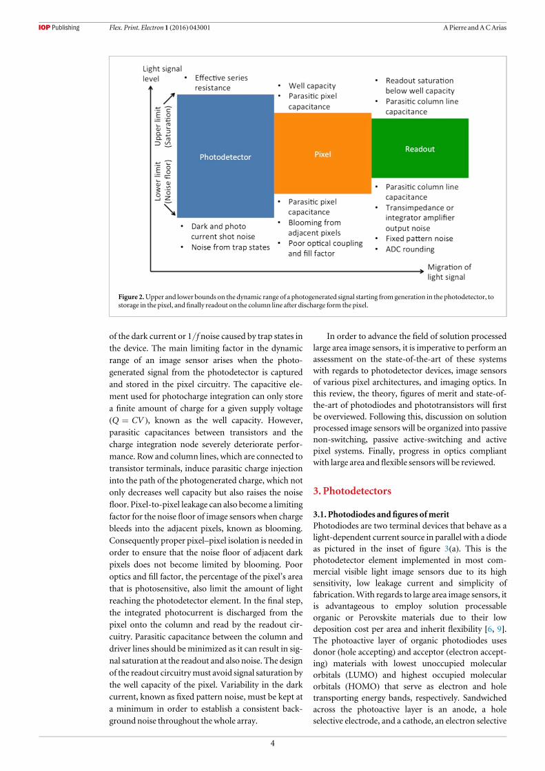
of the dark current or 1/f noise caused by trap states inthe device. The main limiting factor in the dynamicrange of an image sensor arises when the photo-
generated signal from the photodetector is capturedand stored in the pixel circuitry. The capacitive ele-ment used for photocharge integration can only store
a finite amount of charge for a given supply voltage(Q=CV ), known as the well capacity. However,
parasitic capacitances between transistors and thecharge integration node severely deteriorate perfor-mance. Row and column lines, which are connected to
transistor terminals, induce parasitic charge injectioninto the path of the photogenerated charge, which notonly decreases well capacity but also raises the noise
floor. Pixel-to-pixel leakage can also become a limitingfactor for the noise floor of image sensors when chargebleeds into the adjacent pixels, known as blooming.
Consequently proper pixel–pixel isolation is needed inorder to ensure that the noise floor of adjacent darkpixels does not become limited by blooming. Poor
optics and fill factor, the percentage of the pixel’s areathat is photosensitive, also limit the amount of light
reaching the photodetector element. In the final step,the integrated photocurrent is discharged from thepixel onto the column and read by the readout cir-
cuitry. Parasitic capacitance between the column anddriver lines should beminimized as it can result in sig-nal saturation at the readout and also noise. The design
of the readout circuitrymust avoid signal saturation bythe well capacity of the pixel. Variability in the darkcurrent, known as fixed pattern noise, must be kept at
a minimum in order to establish a consistent back-ground noise throughout thewhole array.
In order to advance the field of solution processedlarge area image sensors, it is imperative to perform anassessment on the state-of-the-art of these systemswith regards to photodetector devices, image sensorsof various pixel architectures, and imaging optics. Inthis review, the theory, figures of merit and state-of-the-art of photodiodes and phototransistors will firstbe overviewed. Following this, discussion on solutionprocessed image sensors will be organized into passivenon-switching, passive active-switching and activepixel systems. Finally, progress in optics compliantwith large area andflexible sensors will be reviewed.
3. Photodetectors
3.1. Photodiodes andfigures ofmeritPhotodiodes are two terminal devices that behave as alight-dependent current source in parallel with a diodeas pictured in the inset of figure 3(a). This is thephotodetector element implemented in most com-mercial visible light image sensors due to its highsensitivity, low leakage current and simplicity offabrication.With regards to large area image sensors, itis advantageous to employ solution processableorganic or Perovskite materials due to their lowdeposition cost per area and inherit flexibility [6, 9].The photoactive layer of organic photodiodes usesdonor (hole accepting) and acceptor (electron accept-ing) materials with lowest unoccupied molecularorbitals (LUMO) and highest occupied molecularorbitals (HOMO) that serve as electron and holetransporting energy bands, respectively. Sandwichedacross the photoactive layer is an anode, a holeselective electrode, and a cathode, an electron selective
Figure 2.Upper and lower bounds on the dynamic range of a photogenerated signal starting fromgeneration in the photodetector, tostorage in the pixel, and finally readout on the column line after discharge form the pixel.
4
Flex. Print. Electron 1 (2016) 043001 APierre andACArias

electrode. As shown in step 1 of figure 3(a), the lowdielectric constant of organic materials causes photo-excited electron–hole pairs to become colombicallybound, which is known as an exciton. It’s only whenthis exciton diffuses towards a donor–acceptor inter-face as shown in step 2 that the higher electron affinity(lower LUMO) of the acceptor material and lowerionization potential (higher HOMO) of the donormaterial causes the exciton to dissociate into a freeelectron and hole in the acceptor and donor, respec-tively. Most organic photodiodes use a bulk hetero-junction (BHJ) active layer, which is the mixture ofdonor and acceptor materials in order to increasesurface area across which excitons may be dissociated.The free electrons and holes are then transportedthrough the acceptor and donor and collected at thecathode and anode, respectively, ideally withoutrecombination. Perovskite materials are usually notcomposed of a donor or acceptor components as thedielectric constant for these materials is significantlyhigher than organics, which permits excitons to freelydissociate into free carriers via thermal energy [10].
The figures ofmerit used to assess photodiode per-formance also have a direct impact on image sensorperformance. External quantum efficiency (EQE) isdefined as the ratio of the rate of extracted photo-generated electrons from a device over the rate of inci-dent photons radiated on the photoactive area. EQE istypically expressed as a function of incident lightwavelength as shown in figure 3(b). Alternatively, EQE
can be equivalently expressed as the output current perwatt of irradiance, this is known as responsivity (R).Current density versus bias voltage characteristics arealso instrumental for assessing proper device in darkand illuminated conditions as shown in figure 3(c).Photodiodes are reversed biased (VBias<0 V) to cre-ate a larger electric field in the device to extract carriersbefore recombination. Additionally, reverse biasingthe photodiode results in lower injection current indark conditions (known as dark current) compared tothe photovoltaic biasing regime (VBias>0 V). Anideal photodiode should have a high differencebetween light and dark current at a reverse bias inorder to enable the highest SNR. In terms of deviceperformance, the EQE should be high to create a largelight current and the leakage across the diode shouldbe minimal to minimize dark current. A photodiodethat maintains a high SNR at large reverse bias trans-lates into a larger well capacity since the capacitance ofthe diode itself is used to store charge (more details inthe section on passive active-switching image sensors).Observing current density as a function of light inten-sity enables the determination of dynamic range,which is the range of irradiance over which the photo-diode exhibits a measurable change in photocurrent.This figure of merit can either be expressed as the ratiobetween the highest and lowest light intensity or thatratio in decibel format [3] as shown in equation (2)and illustrated infigure 3(d)
Figure 3. (a)Band diagramof an organic photodiode depicting charge generation and collection and the equivalent circuit. (b)Qualitative depiction of external quantum efficiency (EQE) and responsivity (R) for a photodetector. (c)Typical photodiode current–voltage characteristics in dark and under illumination. (d) Illustration of dynamic range for a photodetector.
5
Flex. Print. Electron 1 (2016) 043001 APierre andACArias

( ) ( )=⎛⎝⎜
⎞⎠⎟
I
IDynamic range dB 20 log . 210
upper
lower
A linear dynamic range response (constant EQEacross a wide range of irradiance) is usually desired forphotodiodes. However, sublinear responses are oftenseen in disordered materials such as organics andnanomaterials [11–13]. While these responses maynot be ideal for certain radiometric applications, theycan be advantageous for improving the dynamic rangeof an imaging system [3] as will be later discussed inthe section on passive active-switching image sensors.The dynamic range of photodiodes is typically limitedby the noise of dark current at low irradiances. Thedark current noise in its simplest form is expressed asthe shot noise of the current flow, which behavesaccording to Poisson statistics. The noise, or standarddeviation, of a Poisson process is defined as the squareroot of the flux of electrons per second. In addition,the equivalent shunt resistance of the photodiode at 0V bias, Rshunt, induces thermal noise. Excessive trapstates within the band gap of the photodiode can leadto 1/f noise on top of shot and thermal noise.Equation (3) shows how dark current and charge trap-ping affect the noise spectral density (S) of a photo-diode with q, kB and T denoting elementary electroncharge, Boltzmann’s constant and temperature,respectively
( )( )
= + +
= + +
⎛⎝⎜
⎞⎠⎟S N N N
qIk T
RN
A
Hz
24
. 3shot2
shunt2
trap2
darkB
shunttrap2
Two equivalent figures ofmerit used to express theperformance of a photodiode at low irradiances arenoise equivalent power (NEP) and specific detectivity(D*). NEP is the theoretical lowest measurable irra-diance (SNR=1) for a 1 Hz integration bandwidth(or equivalently half second integration time accord-ing to Nyquist-Shannon sampling theory [5]).Figure 3(d) qualitatively shows that the NEPmarks thelowest point on the dynamic range. NEP can be quan-tified by equation (4), which is the noise spectral den-sity divided by the responsivity of the photodiode.Specific detectivity is defined by equation (5) and isinversely proportional to NEP and normalized to area(A) since µ µS I A . This area normalization isimportant in order to allow a fair comparison betweenvarious photodiodes since, as previously discussed,SNR increases with area
( )=⎛⎝⎜
⎞⎠⎟
S
RNEP
W
Hz, 4
( ) ( )*⋅
=⎛⎝⎜
⎞⎠⎟D
Acm Hz
WJones
NEP. 5
The frequency response of a photodiode is a figureof merit applicable to image sensors. Typically this ischaracterized by the cutoff frequency ( f3dB), which is
the frequency at which the peak output current from asine-modulated light source is lowered by 3 dB fromlower frequencies. A high cutoff frequency is indica-tive of fast charge extraction from the device, whichminimizes image lag in image sensors [4, 14].
There have been many developments in the litera-ture on solution processed photodiodes, which typi-cally attain EQEs and dark currents anywhere from20% to 60% and 10–1000 nA cm−2, respectively[11, 15]. More recently, many studies have beenaggressively investigating new physical mechanisms tocreate low noise, high frequency, spectrum selectiveand fully printable photodiodes.
Much of the prior art from the organic and Per-ovskite solar cell community on the effect of activelayer film thickness, solvent composition and donor–acceptor ratio on morphology [16–19] and devicephysics [13] was used to obtain similar EQEs in solu-tion processed photodiodes. However, reverse biasdark current and frequency response was rarely inves-tigated in the context of photovoltaics and has beenoptimized for photodiodes in several ways. Increasingthe thickness of the active layer beyond a micrometercan significantly drop the dark current to values below1 nA cm−2 without a significant compromise in cutofffrequency [14, 20]. Reduced dark current alsoachieved when hole and electron blocking layers at thecathode and anode, respectively, are used to improvecharge selectivity at the electrodes [11, 15]. Thisbecomes especially important in low band gap systemswhere Schottky barrier at the electrodes is lower [21].It has been shown that organic interlayers in Per-ovskite photodiode to decrease the dark current tobetween 1 and 10 nA cm−2 under reverse bias whilemaintaining response times of approximately amicro-second [22, 23] as shown in figure 4(a). Subsequentpower spectrum measurements revealed the noisespectral density of these devices is indeed very close tothe shot noise theoretical limit, which is believed to bethe result of surface defect passivation from the inter-layers [22]. Interface engineering is important whenoptimizing frequency response. Arca et al have shownthat frequency response in BHJ organic photodiodesdeteriorates significantly at low irradiances as a resultof carrier trapping at interfaces, which can be amelio-rated by choosing a suitable interlayer [24].
The absorption spectrum of a photodiode can bemade broader to image at longer wavelengths. Con-ventional organic or Perovskite photovoltaic materialsshow a broad absorption with cutoff wavelengths typi-cally around 900 nm. This is because the optimal bandgap for power conversion efficiency is 1.34 eV (∼925nm) according to the Schockley-Queisser limit [25].Gong et al took the first step to synthesizing custom-made polymers for very broadband photodiodes witha spectral response form 300 to 1450 nm [26]. A laterstudy synthesized a polymer with a low cutoff wave-length of 1000 nm for photodiode use [27]. By using asuperior electron-blocking layer, the dark current was
6
Flex. Print. Electron 1 (2016) 043001 APierre andACArias

reduced to a few nA cm–2 while maintaining an f3dB of400 kHz. Quantum dots, which can have low bandgaps, can also be embedded in photodiodes to extendthe responsivity of the device to wavelengths as long as1800 nm [28].
Conversely, it is also possible to narrow the spec-tral response of photodiodes. The drive for color filter-less image sensors has led to the development of mate-rials with narrow absorption bands in the red, greenand blue regions [29–31]. Meredith et al have showthat even broadband materials can be used to createnarrow spectral selectivity by significantly increasingthe active layer thickness [20]. Figure 4(b) shows thatthe lower extinction coefficients of wavelengths nearthe absorption cutoff penetrate further and more uni-formly into the device where electrons are more likelyto be extracted at the cathode. However, the highabsorption well below the cutoff wavelength results ina significant amount of recombination at the front ofthe device as a consequence of space charge accumula-tion of electrons.
The majority of literature on solution-processedphotodiodes utilizes spin coated active layers withvacuum-deposited electrodes on rigid substrates.While synthesizing soluble functional materials is apre-requisite to creating printable devices, it is
important to create printed devices since the printingprocess can present challenges or new opportunitiesnever realized with conventional microfabrication[6, 7]. The discovery of solution-processable workfunction reducing interlayers such as poly-ethylenimine ethoxylated (PEIE) [32] and conjugatedpolyfluorene electrolytes [33] opened many possibi-lities in printed electronics as soluble low work func-tion conductors are not available. Caironi et al initiallyreported fully solution processed photodiodes usinginkjet printing and PEIE to reduce the work functionof the silver or PEDOT:PSS cathode [34, 35]. Organicphotodiodes printed using a combination of bladecoating and screen printing reported by Pierre et alshowedmean dark currents as low as 150 pA cm−2 andspecific detectivities as high as 3.4×10¹³ [36]. Asshown in figure 4(c), these devices displayed high spe-cific detectivity under a large applied electric field incomparison to other devices [37–41], which is impor-tant for maximizing well capacity in image sensors aswill be discussed in the section of passive active-switching image sensors. The bias stability of thesedevices is shown in figure 4(c), which is an importantconsideration in imaging systems as photodiodes arebiased continuously. More information on printing
Figure 4. (a)Organic blocking layers in a Perovskite photodiode and its dynamic response. (b) Filterless organic photodiodes enabledthrough thick active layers and the resulting EQE spectrum. Reprintedwith permission fromMacmillan Publishers Ltd:Nat.Commun. [20], copyright 2015. (c)Detectivity as a function of applied field across the device for various photodiodes cited in thisreview alongwith the bias stress stability of an organic photodiode. (a) and (c)Reprintedwith permission from [22] and [36],respectively. Copyright 2015 JohnWiley and Sons.
7
Flex. Print. Electron 1 (2016) 043001 APierre andACArias

techniques for solution processable electronics can befound in a review byKrebs [7].
3.2. Phototransistors andfigures ofmeritPhototransistors can also be used as the photodetectorelement in image sensors. This device has threeterminals, unlike two-terminal photodiodes, andbehaves like a regular thin film transistor (TFT) in thedark. Such devices consist of a conductive channelwith unipolar source and drain electrodes on eitherside with the conductivity of the channel controlled bya gate terminal. However, the TFT behavior of thesedevices changes upon light exposure for a couple ofreasons.
Phototransistors can operate as a photoconductoras shown in figure 5(a) for a p-type device (hole trans-porting). The transverse field created by the gate elec-trode assists the spatial segregation of photogeneratedelectron–hole pairs. However, since both source anddrain contacts are hole-selective, the photogeneratedelectron stays in the channel while the photogeneratedhole is extracted at the drain. The accumulation ofelectrons in the channel results in a shift in thresholdvoltage, causing more holes to be injected in order toneutralize the electrons [11, 42]. New holes will beinjected into the channel at the source electrode until arecombination event occurs between an injected holeand the photogenerated electron. If the transit time ofa hole across the device (τtransit) is less than the lifetimeof the electron (τlifetime), then multiple holes can beinjected into the channel of the phototransistor for asingle photogenerated electron–hole pair. This
phenomenon, known as photoconductive gain (G),can result in EQEs well over 100% as denoted byequation (6) [11, 42, 43]
( )t t=G . 6lifetime transit/
The response time of phototransistors in the pho-toconductive regime is usually limited by the lifetimeof the minority carrier and not the comparatively fasttransit time of the majority carrier. Consequently,devices that exhibit high photoconductive gain cannotoperate as quickly as a photodiode with the same tran-sit time. Photoconductive gain decreases with increas-ing irradiance for a couple of reasons. The first is thatelectrons generated at low irradiances fill deeper trapstates that have longer recombination lifetimes, withhigher irradiances resulting in electrons filling shal-lower trap states that have shorter lifetimes [44]. Thesecond reason is that the shift in threshold voltage isproportional to the logarithm of the irradiance[11, 45], resulting in decreased sensitivity at higherlight intensities.
Phototransistors can also operate in a charge-trap-ping regime in which photogenerated electrons (in ahole-transporting device) become lodged in deep trapstates in the channel of the device as shown infigure 5(b). This trapping results in a shift in thethreshold voltage of the phototransistor during nor-mal transistor bias sweeps, even after the illuminationhas stopped. The lifetime of these trap states may evenbe as long as days [46]. These electrons can be de-trap-ped through a large gate bias, effectively resetting thephototransistor. For this reason, phototransistors
Figure 5. (a)Hole (red) and electron (yellow)movement in a hole-transporting phototransistor with photoconductive gain and thedynamic response shown to the right. (b)Charge carriermovement in the same phototransistor but operating in a long-term charge-trapping regime.
8
Flex. Print. Electron 1 (2016) 043001 APierre andACArias

operating in charge-trapping mode with exceptionallylong trap state lifetimes are sometimes referred to asmemory devices [46]. Phototransistors often operatein a combination of both the photoconductive gainand charge-trapping regime since both of thesemechanisms involve the lifetime of minority carriersbut at different time scales.
Responsivity is frequently used as a figure of meritfor phototransistors. Yuan et al have closely examinedthe behavior of C8-BTBT phototransistors, whichprovide the highest photoconductive gain seen in lit-erature to the best of our knowledge [47]. One keyobservation is that the photoconductive gain is sig-nificantly higher in phototransistor than in a thin filmphotoconductor of the same device geometry. Thisdifference in gain is speculated as a result of the trans-verse field induced by the gate segregating electronsand holes, thus reducing the probability of recombina-tion. The very long recombination lifetime of elec-trons in C8-BTBT (∼seconds) and high mobility of 20cm2 V s−1 results in a responsivity over 105 A W−1.The low defect density of the highly crystalline semi-conductor also resulted in noise spectral density onpar with the theoretical shot noise limit. However, thelong electron lifetimemeans that the device takes hun-dreds of seconds to turn off unless a large gate pulse isapplied. Yan et al have achieved high gain throughembedding wide band gap metal oxide nanoparticlesin an organic semiconductor [48]. The gain obtained isat most an order of magnitude lower than Yuan et al’s,but the turnoff timewas over 102 times faster.
Photoconductive gain mechanisms can also beimplemented in a photodiode architecture usingembedded nanoparticles. Guo et al initially demon-strated this concept by creating P3HT photodiodeswith a sparse concentration of isolated ZnO nano-particles [40]. Electron trapping in the ZnOunder illu-mination creates photoconductive gain. Additionally,electron trapping near the anode causes significantband bending which results in trap-assisted hole injec-tion to create higher gain as shown in figure 6(a). Theshort travel distance of the carriers in a photodiodestructure also decreases recombination lifetimes tounder 1 ms while retaining a responsivity of over 1000A W−1. It was shown in a later study that a trade-offexists between photoconductive gain and cut-off fre-quency in photodiodes [49]. Low nanoparticle con-centrations led to high gain due to the good isolationof small nanoparticle clusters but significantly longerde-trapping times, whereas high nanoparticle con-centrations led to a more continuous network whichdid not promote good charge trapping but sig-nificantly decreased de-trapping times. Similar reportswere shown for Perovskite [50] and organic [51] andhybrid [52, 53] photodetectors.
While conventional high-performance solutionprocessable TFT semiconductors can be used as
phototransistors, the wide band gap and low absorp-tion coefficient of these materials limits their perfor-mance outside the UV spectrum. Several strategieshave been shown in the literature to address the pooroptical properties of conventional TFTs. The firststrategy is to employ the same BHJ active layermorph-ology frequently used inOPDs in phototransistors. Xuet al have reported a BHJ phototransistor with a cutoffwavelength of 900 nm and high responsivity of over105 A W−1 at light intensities below 100 nW cm−2
[44]. The hole mobility of their devices (0.3 cm2 Vs−1)is significantly higher than that of conventional BHJOPDs (<10−4 cm2 V s−1) [11], which enables aresponse time of ∼40 ms. A similar concept was latershown by Han et al demonstrated a BHJ photo-transistor with a low cutoff wavelength of 1000 nm asshown in figure 6(b) [54]. Another alternative toimprove the optical properties of phototransistors is touse Perovskite materials, which typically show similaroptical properties and improved charge carrier mobi-lity in comparison to organics. Li et al have demon-strated a Perovskite ambipolar transistor with aresponsivity of over 102 down to 800 nm [55]. Thehigh charge carrier mobility of over 1 cm2 V s−1
enabled very fast response times of under 7 μs. Ahybrid device scheme can also be used to leverage theelectronic or photonic properties of each layer. Forinstance, Rim et al deposited a BHJ on top of a highmobility indium gallium zinc oxide TFT to form aphototransistor [56]. A specific detectivity over 1012
Jones was demonstrated for their devices, with mini-mal persistence of photocurrent and at least 7 ordersofmagnitude linear dynamic range.
In addition to the channel of phototransistors,other layers of the device such as the electrodes andgate dielectric are printable. All-printed photo-transistors on a flexible polyimide substrate demon-strated by Kim et al highlight several commonlyused printing techniques as shown in figure 6(c)[57]. Inkjet printing was used to directly pattern thephotoactive material and gate electrode with thegate dielectric uniformly bar coated in between.Reverse offset printing defined the channel geo-metry of W/L=1000 μm/20 μm. This highthroughput printing technique can even createchannel lengths below 1 μm [58]. Self-assemblyprocesses can also achieve sub micron channellengths. Wang et al utilized inkjet printing of solu-bilizing solvents on ultrathin PMMA (a photoresist)to create thick coffee-ring induced ridges [59]. Sub-sequent deposition of metal and removal of thePMMA defines channel lengths of 700 nm, whichgreatly enhanced the responsivity of longer channeldevices since the transit time of injected holes isshorter. A high responsivity of 106 A W−1 with anaverage TFT mobility of 1.2 cm2 V s−1 wasreported.
9
Flex. Print. Electron 1 (2016) 043001 APierre andACArias

4. Passive pixel image sensorswithoutactive-switching
4.1. TheoryPassive pixel sensors transfer the raw photogeneratedsignal from the photodetector element directly to thecolumn line. This direct transfer of the photogener-ated signalmeans that no amplification (gain of unity)of the signal occurs within the pixel as shown infigure 1(a). A passive pixel can use active-switching tointegrate photogenerated charge during the frameperiod as previously discussed in the fundamentalprinciples of image sensors. However, a passive pixelcan also simply consist of a photodetector directlyaddressed by the row and read out instantaneously bythe column line, rather than integrated, as symbolizedfor both a photodiode and phototransistor infigures 7(a) and (b), respectively. The inherit dis-advantage of this design is that the SNR of a non-integrated pixel is significantly lower compared to anintegrating one as mentioned previously in thefundamentals of image sensors. This compromise inthe quality of the signal means that the array can onlybe scanned at impractically slow frame rates. Despitethis disadvantage, constructing passive non-switch-ing image sensors is still a valuable step in
demonstrating the scalability, functional deviceyield, uniformity and performance of photodetectorelements.
Figure 6. (a) Interfacial trapping of photogenerated carriers used to inject charge from an electrode as a gainmechanism. Reprintedwith permission fromMacmillan Publishers Ltd:NatureNanotechnology [40], copyright 2012. (b)Broadband bulk heterojunctionphototransistor. Reprinted by permission fromMacmillan Publishers Ltd: Sci Rep. [54], copyright 2015. (c) Fabrication steps for anall-printed phototransistor. Reprinted from [57], copyright 2014, with permission fromElsevier.
Figure 7. (a)Photodiode and (b) phototransistor-basedpassive pixel architecture for image sensors not using intra-pixel charge integration.
10
Flex. Print. Electron 1 (2016) 043001 APierre andACArias

4.2. Case studiesSolution processable semiconducting polymers revo-lutionized the research field of photovoltaics byenabling the possibility of low-cost, large-area andflexible solar modules [60]. As such, the optimizationof the materials to create high performance solar cellsalso enabled the development of arrays of photodiodes(pixel architecture of figure 7(a)) used as imagesensors. Yu et al were the first to demonstrate thecapability of such solution processed solar cells to actas photodiodes in an image sensor by downscaling theelectrode spacing between each solar cell and increas-ing the total pixel count along a linear array as shownin figure 8(a) as summarized in table 1 [61]. Poly(3-octylthiphene) (P3OT)was used as the donor polymerdue to its absorption over the whole visible spectrum,which was difficult with the wider band gap polymerscommonly used at the time of publication [60]. Thesedevices showed good photodiode behavior (<10 nAcm−2 dark current and 45% EQE at −10 V bias) andsufficiently high uniformity over the 102 pixels in thelinear array to be used as an image scanner. Addition-ally, the high resistivity and high absorptivity oforganicmaterials enabled thin device active layers withnegligible crosstalk between pixels even for an un-patterned active layer. A later account by Xu et al tookadvantage of the mechanical robustness of organic
systems by implementing the same array architectureon a deformable plastic substrate [62]. This wasmotivated by the idea that conformable image sensorscouldminimize the amount of optics that are requiredto focus the image plane on conventional planar imagesensors. Metal grid lines were deposited on thesubstrate by direct pattern transfer of thermallyevaporated gold or silver from a deformedPDMSmold.
Flexible phototransistor arrays have also beenimplemented in a non-switching passive pixel archi-tecture as shown in figure 7(b). Saito et al utilized thephotosensitivity of a conventional pentacene transis-tor to form a photodetector array with a microlensarray on flexible substrate [63]. However, the poorabsorption and responsivity of pentacene to lightrequires high irradiances (>2 mW cm−2) in order tomeasure an appreciable change in on-current. How-ever, Chu et al have recently shown that the choice ofgate dielectric can tune the charge trapping propertiesof DNTT phototransistors to significantly improveimaging performance [64]. Using polylactide (PLA)as the gate dielectric significantly lowers mobilityin the dark, but significantly increases it when photo-generated charges are trapped along with a positiveshift in threshold voltage. This also results in a sig-nificantly faster response time of only 50 ms, which
Figure 8. (a)Reproduced color image scanned by a linear array of organic photodiodes. Reprintedwith permission from [61].Copyright 1998 JohnWiley and Sons. (b)An array of phototransistors based on charge transfer to a semiconductor from a light-absorbing dye. Reprintedwith permission from [65]. Copyright 2016AmericanChemical Society. (c) Light-programmable organicphototransistormemory devices and an imaging array. Reprinted by permission fromMacmillan Publishers Ltd: Sci Rep. [46],copyright 2013.
11
Flex. Print. Electron 1 (2016) 043001 APierre andACArias

Table 1.Properties of solution-processed non-charge-integrating passive pixel image sensors.
Type of photodetector Imagemeasurement Pixel device processing andmaterials Lowest imaged irradiance (μWcm−2)@λ Bending radius (mm) Reference
Photodiode Photodiode current Soluble organic ∼1× 10⁻³ Rigid substrate [61]Photodiode current Evaporated organic 2@633 nm 10 (curved but notflexible) [62]
Phototransistor Channel current fromΔ in conductance Evaporated organic 2× 10³ 20 [63]Channel current fromΔ in conductance andVT Evaporated organic 20@450 nm Flexible but notmeasured [64]Channel current fromΔ in conductance Soluble light absorber on evaporated organic 1.2@450 nm 1 [65]
Memory Photodiode current (after light exposure) Evaporated resistive switchmemory on soluble organic 1.5 Flexible but notmeasured [66]Channel current fromΔ inVT (after light exposure) Evaporated organic on soluble organic 40 Flexible but notmeasured [46]
Inorganic Photoconductive current Blade coated Perovskite 30@550 nm 5 [67]Photodiode current Sputtered ferroelectric 1×10⁵@658 nm 32 [69]Channel current fromΔ in conductance CVD/sol-gel nanowires ∼100 Rigid substrate [70]
12
Flex.Print.E
lectron1(2016)043001
APierre
andACArias

may be practical at video frame rates. The absorptionspectrum of the aforementioned phototransistorimage sensors is often limited to blue and UV wave-lengths as a result of the large band gap of high perfor-mance organic semiconductors such as pentacene andDNTT. Liu et al have demonstrated that the responsiv-ity of conventional phototransistors can be sig-nificantly enhanced by inserting a strong absorbinglayer on top of a high mobility semiconductor asdepicted in figure 8(b) [65]. A ruthenium complexwith a broad absorption spectrum is used to enhancethe responsivity of the phototransistors by a factor ofalmost 103 in the off-regime with a drop inmobility byonly a factor of 2 in the on-regime. This enables thecapture of images at a relatively low light irradiance of1.5μWcm−2.
Memory devices can also be used as passive pixelimage sensors. These devices enable global shutterarray operation, which is the simultaneous capture oflight information on all pixels across an array, asshown in figure 1(c). Global shutter reduces motionartifacts seen in a rolling shutter sequence illustrated infigure 1(b) since row addressing during image captureis not necessary. Nau et al have demonstrated a passivepixel array consisting of pixels with an organic non-volatile resistive switch in series with an organic pho-todiode [66]. A sufficiently large voltage pulse is sup-plied across the pixel during illumination. The voltagedrop across the photodiode decreases with increasingillumination (due to its higher photoconductivity),which increases the voltage across the resistive switch-ing element beyond a threshold voltage that then trig-gers a change in resistance. The irradiance that thepixel sensed can then be readout at a later time byexamining the resistance of the pixel at a small bias,and reset by applying a large bias for the next image.Charge trapping can also be used within a device tocreate long-term storage memory devices. Zhang et alhave shown that inserting an electron acceptor at thesemiconductor-dielectric interface of a photo-transistor enables long-term storage of photo-generated electrons [46]. The electrons areaccumulated at the interface with a positive gate bias asshown in figure 8(c). This accumulation results in apositive threshold voltage shift with increasing lightintensity, which can be sensed at low gate voltages andreset at high negative biases. Optimization of the elec-tron accepting layer led to long charge retention, withthe sensed current only decreasing by 8% after 20 000s, and high performance transistor properties withmobility over 2 cm2 V s−1 and on-off ratios of5×106. Such high performance transistor and pho-todetector properties in a single device could alsoenable active pixel circuits.
While organic materials have long been the choiceof solution processable and flexible systems, photo-diode image sensor arrays have recently been demon-strated with novel photoactive materials. Perovskiteshave been shown to form high performance
photoconductor image sensors through blade coatingby Deng et al [67]. Not only is the material stable forweeks in air, it is extremely resilient to strain with noobservable change in current–voltage behavior after10 0000 bending cycles. Ferroelectrics are a class ofmaterials that have been extensively studied for appli-cations of memory in microelectronics [68] but canalso be used as large area image sensors as demon-strated by Chin et al [69]. Their initial results showphotodiodes constructed on flexible steel foil with lowdark currents. Solution processable II–VI semi-conductor nanowires have also been processed into apassive image sensor from sol-gel by Liu et al [70].Their phototransistors have mobilities ranging from 4to 28 cm2 V s−1 depending on the S:Se ratio, whichalso adjusts the band gap. Using these tunable bandgaps, they were able to fabricate a multicolor imagerwithout the need of optical filters.
5. Passive pixel image sensors capable ofactive-switching for charge integration
5.1. TheoryPassive image sensors can be implemented with anactive-switching backplane that enables integratingphotogenerated charge during the period of a frame.As previously mentioned, integration of photogener-ated charge significantly improves the SNR of the lightsignal from a pixel compared to direct currentsampling at a given frame rate. Figure 9(a) illustratesthe array layout and pixel architecture for an active-switching passive pixel sensor, a transistor in serieswith a photodiode (1 T), and charge amplifier on eachcolumn to sample the integrated charge. The pixelcircuit with all relevant capacitances is shown infigure 9(a) as well. The intrinsic capacitance of thephotodiode (CPD) is used as the integrating capacitor.Photodiodes are ideal for 1 T pixels since the largesurface area and short spacing of the electrodesprovides the large capacitance needed to maximizewell capacity.
The ideal operation of a 1 T pixel is illustrated infigure 9(b). When the TFT is on, the voltage of thephotodiode anode (VPD) is set to zero while the cath-ode is biased at a positive voltage (making the devicereverse biased). After the TFT is closed, VPD increasesas CPD accumulates photogenerated charge during theframe period. Opening the TFT discharges the accu-mulated photogenerated charge and resets the photo-diode back to its original reverse bias for the nextframe. The ideal discharge rate is governed by a timeconstant R C ,on PD where Ron is the resistance of theTFT in the linear regime. The transistor typicallyremains open for several time constants in order todischarge as many carriers as possible to minimizeimage lag. The off-state resistance of the TFT, R ,off
must also be high to ensure that R Coff PD is much
13
Flex. Print. Electron 1 (2016) 043001 APierre andACArias

greater than the frame period to minimize dischargeduring the integration.
Parasitic capacitances substantially affect the per-formance of image sensors by inducing parasiticcharge injection that creates readout noise and lowerdischarge rates. The drain-source capacitance is extre-mely small in TFTs and thus has a negligible effect onpixel performance. Additionally, minimal parasiticcharge injection occurs from bias-column line capaci-tances since the column line is grounded and the biasvoltage is constant. However, the gate-drain capaci-tance (CGD) slows the switching speed of the transistorand induces parasitic charge transfer onto the photo-diode [4]. The time constant of the discharge changesto ( )+R C C ,ON PD GD and VPD decreases by
DC V CGD G PD/ when the pixel enters integration mode(TFT off) as shown in figure 9(b), which limits wellcapacity. Gate-source (CGS) capacitance results fromoverlapping gate and source electrodes and also fromintersecting row and column lines. Since the columnline is connected to virtual ground from the chargeintegrator a parasitic charge of DC VGS G is injectedonto the column line when the TFT is turned on. Itshould be noted that the mean value of the charge onthe column line during sampling time is the same for
both the ideal and parasiticmodel shown in figure 9(b)since VG returns to the same value as at the start of theframe period. Despite the reset of the voltages, para-sitic charge injection still induces noise that increaseswith CGD and CGS according to equation (7). This willlimit the SNR from the sensor in form of readout noisepreviously shown in equation (1)
( ) ( )= +Q K T C C . 7parasitic noise B GS GD
Additional considerations need to be taken intoaccount when implementing disordered materials in a1 T image sensor architecture. Many organic, Per-ovskite and other disordered semiconductors exhibitdecreased responsivity with increased irradiance ordecreased applied bias. This nonlinear responsivityprevents early saturation under bright light and lessphotogenerated charge is added as well capacity isapproached (since the photodiode voltage drop is lowat well capacity). These effects can increase thedynamic range of a 1 T image sensor at a given framerate. On the other hand disordered materials trap asignificant amount of charge in slow-releasing deepstates, leading to image lag effects between frames [4].Bias stress, which is the gradual accumulation of trap-ped charge causing a drift in threshold voltage, is a
Figure 9. (a) 1Tpixel architecture, a charge-integrating passive pixel, showing the integrating capacitor of the photodiode (CPD) andparasitic capacitances. (b)Drive voltage (VG), photodiode node voltage (VPD), and charge on the column line (QC) during pixeloperationwith parasitic effects.
14
Flex. Print. Electron 1 (2016) 043001 APierre andACArias

concern in TFTs during prolonged use. While dis-ordered TFTs with many trap states are used in large-area applications, it has been shown that low dutycycle operation of TFTs similar to the operation ofsuch devices in a 1 T image sensor significantly reducesbias stress as the short turn-on time prevents carriersfrom being lodged in deep trap states [71]. Moredetails on passive pixel image sensor design andoptimization using disordered materials can be foundin literature on large-area amorphous silicon x-raysensors [4].
5.2. Case studiesMany of the reported of 1 T image sensors in theliterature onlymeasure performance inDCmode [72–76] despite the fact this architecture enables chargeintegration within a pixel, making it practical tocapture images at video frame rates. Despite thisdrawback, the literature on solution processable,flexible and large area 1 T image sensors and pixelsshows tremendous efforts in the heterogeneous inte-gration of high performance photodiodes and TFTs assummarized in table 2.
Horizontal (side-by-side) integration of the pat-terned photodiode and TFT is the simplest designfrom a fabrication layout perspective. However, hor-izontal integration of these two devices means thatphotodiode active area must be sacrificed to accom-modate the TFT. This presents a reduction in fill fac-tor, the fraction of an image sensor’s surface area thatis photosensitive. Nausieda et al created a 1 T pixelusing thermally evaporated pentacene TFTs and aninkjet printed photoconductor on inter-digitated elec-trodes [75]. One of the major tradeoffs for the hor-izontal integration was patterning the pentacene byetching to make room for the photoconductor, whichdecreased the on-off ratio and mobility by an order ofmagnitude. Photoconductors can replace photodiodesin 1 T pixels provided the devices have a low dark cur-rent and sufficiently high capacitance to maximizewell capacity. Renshaw et al and Tong et al have shownmonolithic integration of thermally evaporated TFTsand photodiodes on lithographically-patterned elec-trodes as depicted in figure 10(a) [77, 78]. A dischargetime constant of 400 μs was achieved with a TFTmobility of 0.1 cm2 V s−1 and pixels were able to senselight levels as low 250 nW cm−2 at DC [78]. Mal-inowski et al [76] used the same pixel design and deviceactive materials (SubPc/C60 for the photodiode andpentacene for the TFTs) as the aforementioned pub-lications [77, 78] to create a large area 32×32 pixelimage sensor. Image sensors with 200 μm and 1 mmpixel pitch showed similar EQE but lower dark currentdensity for the larger pixels.
Solution-processable organic photodiodes sim-plify the fabrication process of image sensors since sev-eral steps of vacuum deposition can be replaced withprinting or spin coating. Additionally, solution-
processed photodiodes achieve comparable or evenbetter photodiode performance in comparison to theirthermally evaporated counterparts [11]. For instance,Takahashi et al constructed a horizontally integrated 1T image sensor by spin coating a BHJ photoactive layerover an array of carbon nanotube TFTs for x-ray sen-sing [73]. Openings between the TFTs defined thephotoactive area as shown in figure 10(b), a scintillatorwas placed in front of the array to down-convert x-raysto green light. Low light intensities approaching 1 μWcm−2 weremeasured inDC, with negligible changes inperformance down to a very small bending radius of 2mm (such flexibility is made possible by a thin poly-imide substrate of 24 μm). The high mobility of theTFTs (17 cm2 V s−1 average) enables a turn on time ofapproximately 1 ms, however the integration of pho-togenerated charge was not assessed. Gelinck et alassessed the performance of image sensors of a similardesign to Takahashi et al but with organic TFTs incharge integration mode on a flexible substrate [79].TFTs were processed from a pentacene precursor andpatterned with plasma etching, resulting in deviceyields over 99%, an average mobility of 0.2 cm2 V s−1
and negligible crosstalk. This enabled images to becaptured at 6.7 Hz at a low light intensity of 1.1 μWcm−2. The absorption spectra of the photodiode canalso be tuned to suit a wavelength outside the sensitiv-ity of conventional materials. Rauch et al demon-strated that PbS quantum dots embedded in a P3HT:PC60BM BHJ photodiodes with amorphous siliconTFTs enabled video capture at 5 frames per second at awavelength of 1310 nm [28]. This wavelength is welloutside the absorption spectrum of organic semi-conductors and silicon. Similar to Rauch et al, Baierlet al also demonstrated that the cutoff wavelength ofP3HT:PCBM can be increased to 900 nm by dopingthe active layer with Squaraine [80].
Vertical integration of the TFT and photodiode,with the photodiode active area not covered by theTFT, is the most ideal pixel design since this enablesthe highest possible fill factor. One method of manu-facturing an image sensor of this architecture is by fab-ricating the photodiodes and TFTs on separatesubstrates then laminating them together with elec-trical connections through vias as shown by Someyaet al [72]. This enabled the fabrication of a conform-able sheet scanner with the photodiode size scalabledown to 50 μm. Additionally, laminating these sheetsback-to-back could improve mechanical reliabilitysince this places the stress neutral plane where thephotodiodes and TFTs are located. Alternatively, ver-tical integration can be achieved by directly fabricatingone device on top of another in such a way that thephotodiode area is not obstructed. Ng et al deposited aBHJ photoactive layer on top of an amorphous siliconTFT array (mobility 0.8 cm2 V s−1) followed by a layerof ITO to form a top-illuminated x-ray sensor [14].The photodiodes, which have dark currents less than 1nA cm−2 and an EQE of 35%, have a large fill factor of
15
Flex. Print. Electron 1 (2016) 043001 APierre andACArias

Table 2.Properties of solution-processed passive pixel image sensors capable of intra-pixel charge integration.
Pixel architecture Pixel device processing Frame rate (Hz)@ light conditions Lowest imaged irradiance (μWcm−2)@λ Bending radius (mm) Reference
1 T:Horiz integwith patterned photodetector Evaporated TFT, inkjet photoconductor DC@1mWcm−2 1× 10²@ 530 nm Rigid substrate [75]Evaporated TFT, evaporated photodiode 60ms light pulse decay (single pixel) 0.25@578 nm (DC) Rigid substrate [77]Evaporated TFT, evaporated photodiode 400μs readout (single pixel) 12.5@580 nm (DC) Rigid substrate [78]Evaporated TFT, evaporated photodiode DC@130μWcm−2@ 532 nm 3@532 nm Flexible but notmeasured [76]
1T:Horiz integwith blanket deposited photodetector Soluble TFT, soluble photodiode DC@100μWcm−2@ 535 nm 2.5@535 nm (DC) 2 [73]Soluble TFT, soluble photodiode 6.7@∼1μWcm−2 1.1@550 nm Flexible but notmeasured [79]a-Si TFT, soluble photodiode 5@ 1.6mWcm−2@ 1,310 nm 0.6@1,150 nm (DC) Rigid substrate [28]
1T: Vertical integration Evaporated TFT, evaporated photodiode DC@80mWcm−2@white light 4× 10⁴@white light Flexible but notmeasured [72]a-Si TFT, soluble photodiode 10 Theoretical NEPof 30 pWcm−2 25 [14]Evaporated TFT, soluble photodiode DC (single pixel) 5× 10⁴@white light Flexible but notmeasured [74]CMOS transistor, soluble photodiode 100@ 535 and 850 nm 70@535 nm Rigid substrate [80, 81]
Phototransistor Channel current fromΔ inVT 1@NA NA Flexible but notmeasured [85]
16
Flex.Print.E
lectron1(2016)043001
APierre
andACArias

76% over the whole array of 180×180 pixels with apitch of 340 μm. Additionally, the symmetry of elec-tron and hole mobility limits the build-up of spacecharge near one of the electrodes. This build-upwouldhave significantly reduced the internal electric field inthe rest of the device, slowing charge extraction fromthe photodiode. This symmetry in mobility enables atheoretical maximum video rate of 500 Hz for the fullarray (even though 10 Hz was used for the actualimage). Additionally, this array was fabricated on apolyethylene naphthalate substrate with processingtemperatures below 150 °C and demonstrated a 2.5cm bending radius before performance degradation.Alternatively, the TFT can be deposited on top of a
bottom-illuminated OPD as demonstrated by Jeonget al [74]. The aluminum cathode shields the TFT fromthe light, avoiding any undesired phototransistoreffects. A 1mm thick PDMS layer was placed betweenthe OPD and TFT in order to electrically isolate themand chemically protect the OPD during fabrication ofthe TFT. While the charge integrating performance ofthis pixel was not investigated, the pixel responsivityshowed negligible drift during 5 min of operation.Vertical integration of active-switching passive imagesensors has also been demonstrated on organic-CMOS hybrids by Baierl et al [80, 81]. Top-illumi-nated OPDs were created by spray coating P3HT:PCBM then highly conductive PEDOT:PSS on top of
Figure 10. (a)Monolithic integration of an organic thinfilm transistor (TFT) and organic photodiode (OPD) to form a 1T pixel alongwith the dynamic response. Reprinted from [78], copyright 2011, with permission fromElsevier. (b) Flexible organic photodiode-carbon nanotube TFT 1T image sensor. Reprintedwith permission from [73]. Copyright 2013AmericanChemical Society. (c)Top-illuminated spray-coated organic photodiodes on top of a CMOS chip to form ahybrid image sensor. Reprinted by permission fromMacmillan Publishers Ltd:Nat. Commun. [80], copyright 2012.
17
Flex. Print. Electron 1 (2016) 043001 APierre andACArias

an aluminum electrode on theCMOS chip as shown infigure 10(c), with a mean EQE above 40% underreverse bias and negligible crosstalk between pixels(0.26%). A detailed noise analysis confirmed thatflicker noise (also known as 1/f noise) is the dominantsource of noise as a result of charge trapping and de-trapping. However, it remains unclear as to whetherthis noise is primarily the result of traps in the transis-tor or OPD. Finally, vertical integration can beachieved by fabricating transistors transparent to thespectrum of interest. This design concept is well exe-cuted with metal oxide transistors due to their largeband gap [82]. Sakai et al demonstrate that it is possibleto create an image sensor using a transparentInGaZnO TFT and an organic photoconductor in a 1T pixel design [83]. While all the layers were vacuumdeposited in this report, prior art on transparent metaloxide TFTs [82, 84] suggests that it is possible to createprinted versions of these devices.
Phototransistors can also behave as charge inte-grating pixels. Milvich et al have demonstrated thatconventional DNTT transistor arrays can be used asphototransistors without modification of the devicestructure [85]. Light is detected by observing the shiftin threshold voltage while a large positive voltage isapplied to the gate to integrate trapped electrons. Theshift in threshold voltage increases with integrationtime but eventually saturates for long integration peri-ods. Additionally, the rate of threshold voltage shift isinversely proportional to channel length resultingfrom the fact holes are extracted more quickly in shortchannel devices, decreasing the risk of recombinationwith electrons. However, the deep trap states of theelectrons causes slow refresh rates of atmost 1Hz.
6. Active pixel image sensors
6.1. TheoryAn active pixel architecture, which is used in mostcommercial image sensors [3], provides both active-switching for charge integration and intra-pixel ampli-fication. A general understanding of circuits is impor-tant in order to understand the amplificationmechanisms. An active pixel typically consists of aphotodetector element connected to a transistor in asource follower (also known as common-drain) con-figuration as shown in figure 11. Photodiodes areconventionally used in active pixel architectures due totheir large photoactive area and high internal capaci-tance, which maximizes the well capacity of the pixel.Despite this conventionalism, the photogeneratedsignal source is simply labeled as a photocurrentsource, IPhoto, in figure 11 since phototransistors andphotoconductors have recently been shown in activepixels [86–90]. VPhoto changes as charge from thephotodetector element is accumulated at this nodeaccording to equation (8), where Qphotogenerated is theamount of photogenerated charge and Cphoto and CG,
SF are the photodetector and the source followertransistor’s (TSF) gate capacitance, respectively
( )=+
VQ
C C. 8Photo
photogenerated
Photo G,SF
A row-select transistor, TRow, opens access fromthe source follower to the column line. Vphoto, whichlies at the gate of the source follower transistor, is thendirectly transferred to the column line because thevoltage gain of a source following amplifier is≈1. Thesource following amplification works provided thatthe bias resistance at the base of the column, R, ismuch greater that the transistor channel on-resist-ance. Even though there is no voltage amplification,the source follower supplies an abundant amount ofcurrent to counteract the effect of parasitic capaci-tances along the column line, CBus, with the assistanceof a bias current source on the column line, ICol Bias.The charge amplification from the source follower topreserve Vphoto on the column line gives meaning tothe term ‘active’ in active pixel. Additionally, a resettransistor, TReset, is needed to discharge the integratedphotogenerated charge after reading the voltage out-put from a row of pixels. This reset operation operatesthe same way as the 1 T pixel discussed in the previoussection. These three transistors comprise the three-transistor pixel (3 T), the building block of all activepixel architectures [3]. The fundamental disadvantage
Figure 11.Active pixel architecture of a 3 T image sensor,comprised of reset, source follower, and row-select transis-tors. The equivalent circuit of the photodetector is shown, asis the bias current source for voltage readout on the columnline.
18
Flex. Print. Electron 1 (2016) 043001 APierre andACArias

of the 3 T architecture is the rolling shutter effectbecause the integration of photogenerated charge can-not be paused in the pixel. More advanced pixel archi-tectures (4, 5 and 6 T) employ a transfer gate, whichenable a global shutter since charge is simultaneouslytransferred to the source follower gate node for all pix-els in the array and holds that value during pixel read-out [3]. More detail on active pixel architectures andoperation may be found in literature published byHolst et al [3].
6.2. Case studiesThe active pixel sensor just discussed with a photo-diode element is the most common pixel architecture,yet little of it has been demonstrated in the literaturefor solution-processed image sensors as seen fromtable 3. Tedde et al have shown a hybrid system byblade coating P3HT:PCBM on top of an amorphoussilicon TFT active pixel array [91]. Not only couldprinting the photodiode layer reduce cost, it also canbe used to create a vertical pixel structure demon-strated by Ng et al [14] that increases pixel density andmaximizes fill factor. While the pixel architecture isidentical to that shown in figure 11 a charge amplifierwas placed at the base of each column in order todirectly integrate the current coming from the pixel.This approach increases the complexity of the outputelectronics since the voltage is not simply sampled onthe column line. However, the pixel transistorsamplify the photogenerated charge to the columnwhere it is readout by charge amplifiers. This amplifi-cation is proportional to the transconductance of thesource-following transistor in the pixel. It was foundthat larger channel widths translate into higher gainwith a maximum charge gain of 9.2. The increase ingain decreases the NEP from 6 μW cm−2 for thecontrol active-switching passive pixel sensor to 1 μWcm−2 for the active pixel sensor.
Active pixel architectures may also be constructedwith photoconductive elements. The active pixelarchitecture pictured in figure 12(a) from Wang et alplaces an organic light-dependent resistor and a light-insensitive resistor in a voltage divider configurationwith the output connected to the gate of a pentaceneTFT [87]. The TFT is operated as a transconductanceamplifier, with the signal from the pixel read out as thecurrent passing through the TFT. A reset transistor isunnecessary since this image sensor does not operatein a charge-integrating mode. The output of the volt-age divider is just below the onset voltage of the TFTunder dark conditions and passes the threshold volt-age of the TFT under high irradiances. This placementof output voltage from the voltage divider results in alarge dynamic range of pixel current since the TFT isbiased through the subthreshold regime. As a con-sequence irradiances as low as 2μWcm−2 aremeasur-able. The transconductance gain of the TFT results in ahigh amplification of the current passing through the
light-dependent resistor of well over 104 over a widerange of irradiances. Finally, these devices displayextreme mechanical durability down to a bendingradius of tens of micrometers when transferred to a 10μmthick PET substrate.
Phototransistor-based voltage divider active pixelshave also been shown [86, 88, 89] to operate analogousto the design shown byWang et al [87]. The increasingamount of literature on the high photoconductive gainin phototransistors makes them a good candidate forachieving high SNR. Additionally, the ability to set thechannel resistance of the transistors to match that ofthe phototransistor enables a larger dynamic range.Phototransistors are also easier to integrate in activepixel architectures than photodiodes due to the similardevice design and geometry as the conventional tran-sistors used for amplification. Kim et al created ahybrid non-integrating active pixel consisting of metaloxide TFTs for amplification and a spin-coatedorganic phototransistor as shown in figure 12(b)[88, 89]. Exposing deepUV light through a photomaskwas used to active the metal oxide TFTs and isolate theorganic phototransistor. The phototransistor, which isbased on diF-TESADT, exhibits a specific detectivityof≈1012 Jones. This phototransistor was connected inseries with a low transconductance TFT (low channelwidth-length ratio) to form a voltage divider with theoutput going to the gate of a high transconductanceTFT. This circuit design led to a high current gain of≈100, effectively boosted the theoretical specificdetectivity of the pixel from≈1012 Jones of the photo-detector to a high value of ≈1014 Jones. However,future studies will need to be undertaken to determinehow noise from the TFTs may limit this detectivity[92]. The array also displayed extreme mechanicalrobustness as it was fabricated on a 3 μm thick poly-imide substrate, showing no degradation in perfor-mancewhen bent down to a 1mm radius. Zhiyong et alpreviously displayed phototransistor-based active pix-els using the same pixel architecture as Kim et al butusing inorganic semiconducting nanowires [86]. Thephototransistor is a single CdSe nanowire, with a cur-rent output∼1 nA at 10mW cm−2. A current amplifi-cation of over 3×10⁵ is achieved by placing a highresistance transistor, consisting of several Ge/Si core/shell nanowires, and the CdSe phototransistor in avoltage divider configuration with the output leadingto a high transconductance transistor consisting ofmany thousands of Ge/Si core/shell nanowires.Whilethe semiconductors were not deposited from solutionnor was the substrate flexible, advances since the timeof publication on solubilizing inorganic nanowiresand printing them could enable a printable and flex-ible version of this image sensor [70, 93].
Solution processable materials can also be inte-grated in an active pixel architecture onCMOS and arealready finding their way to the market. For instance,numerous recent reports from Panasonic, a large pro-ducer of image sensors and cameras, reported the
19
Flex. Print. Electron 1 (2016) 043001 APierre andACArias

Table 3.Properties of solution-processed active pixel image sensors.
Pixel architecture Pixel device processing Pixel gain (type) Frame rate (Hz)@ light conditions
Lowest imaged Irradiance (μWcm−2)@λ
(if known) Bending radius (mm) Reference
3 T: Photodiode a-Si TFT, blade coated photodiode 9.2 (charge) 100@10μWcm−2@ 522 nm (singlepixel)
1@522 nm Rigid substrate [91]
1T: Voltage divider Evaporated TFT, photoconductor & light-dependent
resistor
2× 10⁵ (current) [email protected]−2@white light 2@white light 5×10⁻³ [87]
3T: Voltage divider Soluble TFTs, soluble phototransistor 100 (current) [email protected]−2@white light 170 1 [88, 89]CVD+contact printed TFTs&phototransistor 3× 10⁵ (current) [email protected]−2 white light 400@white light Rigid substrate [86]
Beyond 3T CMOS transistors, organic photoconductor NA 60@123 dBdynamic range NA Rigid substrate [90]CMOS transistors, organic photoconductor NA [email protected] dBdynamic range (global
shutter)NA Rigid substrate [94]
20
Flex.Print.E
lectron1(2016)043001
APierre
andACArias

integration of organic photoconductive films [90, 94].Nishimura et al integrated an organic photo-conductive film on top of a CMOS active pixel archi-tecture similar to the 3 T design but with an extratransistor to form a feedback loop from the columnamplifier in order to minimize noise [90]. Each pixelalso consists of two sub-pixels, one large-area highsensitivity pixel and another small-area high satur-ation pixel for sensing high irradiances. These combi-nation of these two sub-pixels enables the imagesensor to produce high quality images with a widedynamic range of over 120 dB on a simultaneousphoto capture as shown in figure 12(c). Shishido et alformed an organic photoconductor with a commonITO electrode for all pixels on top of their CMOSarray, with each pixel consisting of the basic 3 T archi-tecture plus a photogenerated charge storage capacitorand feedback transistors similar to Nishimura et al tominimize noise [94]. Photogeneration of charge iscontrolled by the bias on the ITO electrode, which
enabled a global shutter for the image sensor. Solubleinorganic materials are also finding their way intoimage sensors. InVisage Technologies is a companycreating solution-processed quantum dot films on topof CMOS based on prior art in quantum dot photo-detectors [95]. The company claims that the decreas-ing responsivity of these detectors with increasingirradiance causes these pixels to reachwell capacity at ahigher irradiance, which enables a wider dynamicrange [96].
7.Optics for large area andflexible arrays
The impact of printed, large area and deformableimage sensors is not limited to the sensor itself, butalso affects the whole camera system. The modularnature of hybrid material system image sensors andtheir ability to conform to certain shapes presentsmany opportunities to improve and simplify the opticsof cameras.
Figure 12. (a)Active pixels using light-sensitive resistive voltage dividers tomodulate the conductance of an organic thin filmtransistor are implemented as image sensors. Reprint with permission from [87]. Copyright 2015 JohnWiley and Sons. (b) Integrationofmetal oxide thinfilm transistors and organic phototransistors to form active pixel image sensors. Reprintedwith permission from[88]. Copyright 2016 JohnWiley and Sons. (c)Hybrid organic photodetector-CMOS transistor image sensorswith high dynamicrange. © 2016 IEEE. Reprinted, with permission from [90].
21
Flex. Print. Electron 1 (2016) 043001 APierre andACArias

Color filters are essential in image sensors toobtain images in color. The most common filterdesign is the Bayer filter shown in figure 13(a) [3, 12],which is a periodic array of color filters with its unitcell (denoted by white dashed lines) consisting of onered (R), one blue (B) and two green (G) light-sensitivepixels. Two G filters are used in the Bayer unit cellsince the photopic response of the human eye is mostsensitive to green light. Four pixels are interpolated atthe corner of each pixel to determine the color asshown infigure 13(a). However, the orthogonal natureof printing and vacuum-deposition techniques allowsfor highly modular pixel designs not possible or tootedious in silicon processing. Pixels with differentRGB filters or different photodetector spectral sensi-tivity can be vertically stacked with these new materialsystems, which increases the areal efficiency of the sen-sor. Researchers at NHK science and technicalresearch laboratories have pioneered this concept fororganic photodiode and ZnO TFTs [29–31]. Their
initial study focused on formulating organic photo-diode small molecules with absorption selectivity inthe R, G and B regions [29]. These photodiodes hadtransparent electrodes on both sides so that they couldbe vertically stacked. The incident light passedthrough B, G, and R-selective photodiodes in thatorder since the shorter-wavelength photodiodes alsoact as optical filters for the longer-wavelength photo-diodes below. Finally, active-switching passive pixelimage sensors composed of R, G or B-selective photo-diodes and ZnO TFTs were fabricated on separateglass substrates and vertically stacked in the sameorder as the photodiodes as pictured in figure 13(b)[30, 31]. Videos were captured at a frame rate of 30 Hzwith no noticeable image lag for a 128(columns)×95(rows) array with 100 μm pitch. Lim et al from Sam-sung Electronics have shown that it is possible todeposit a G-selective OPD on top of a R andB-selective silicon photodiodes on aCMOS image sen-sor [97]. This sensor design preserves the 2:1:1 G:R:B
Figure 13. (a)TheBayer filter pattern, which ismost common in commercial image sensors. (b)Vertically-stacked blue-, green-, andred-sensitive pixels in a pixel that are used to form an image sensor. Reprintedwith permission from [31]. Copyright 2011The JapanSociety of Applied Physics. (c)Adeformable passive pixel image sensor that can conform to the focal surface of a lens. Reprintedwithpermission from [99]. Copyright 2011National Academy of Sciences of theUnited States of America. (d)Microlens array for thinplanar imaging optics. Reprintedwith permission from [102]. Copyright 2014 Society of PhotoOptical Instrumentation Engineers.
22
Flex. Print. Electron 1 (2016) 043001 APierre andACArias

ratio of the original Bayer filter pattern that is optimalfor photopic vision sensitivity while minimizing thearea of the Bayer unit cell by a factor of two since agreen pixel is stacked over a R andBpixel.
The mechanical flexibility of image sensors notonly enables mechanically-robust sensors, but also aparadigm shift in camera optics. Biological vision sys-tems, whether the single-aperture eyes of humans orcompound eyes of insects, have the photoreceptorsplaced along a curved focal surface onwhich the imageis captured [8]. Having a conformal imaging surfaceconsiderably simplifies the optics for animal visionsince light only needs to travel through one lens toform a focal surface. On the other hand, conventionalcameras are comprised of many compound lenses inorder to make a planar focal plane. Imaging systemswith a large N (N=lens focal length/entrance pupildiameter), also known as the f-number, do not requireasmany lenses to planarize the imaging plane since theincident light is more perpendicular to the imagingsurface, which also results in a large depth of field.However large N systems reduce the amount of lightentering the camera and are bulky since the focallength of the lens can be upwards of tens times theentrance pupil diameter. Small N systems are morecompact and let in more light, however the incidentlight at the edges of the sensor arrives at low angles,which greatly reduces the depth of field. Increasing thedepth of field for low N cameras requires more opticsin order to planarize the focal surface. Single-aperturecamera lenses become evenmore complex and expen-sive when a larger sensor is needed for increased lightsensitivity. These issues have been addressed by creat-ing single lens single aperture cameras with a stretch-able hemispherical image sensor [98, 99]. Thesesensors were fabricated by first creating a passive arrayof silicon photodiodes with compressible inter-connects on a silicon wafer then transferring it to aPDMS membrane as shown by Ko et al [98]. Theradius of curvature of the image sensor is proportionalto the pressure behind the membrane. Jung et aldemonstrated that curving the image sensor to closelymatch the focal surface created by the lens significantlyimproves the quality of the image by ensuring afocused image across the sensor as shown infigure 13(c) [99].
While flexible image sensors can reduce the com-plexity of optics down to single lens imaging systems,single-aperture cameras can become expensive andbulky with increasing entrance pupil diameter. This isespecially a concern when implementing large-areaimage sensors in order to improve image quality whileminimizing size and cost. Numerous reports in the lit-erature address this issue through the use of microlensarrays to create bio-inspired compound eye systems[8, 100–104]. Brückner et al fabricated microlens sys-tems designed to be directly integrated on top of animage sensor that reduces the focal length of the sys-tem by at least 50% [100–102]. As illustrated in
figure 13(d), each of thesemicrolenses captures a smallportion of the image that partially overlaps with adja-cent microlenses, and the final image is formed bystitching these sub-images together. While this imagesegmentation means there exists some dead spacebetween the images of eachmicrolens, this issuewouldbe little concern for printed large-area sensors com-pared to the high processing cost per area of silicon [6].Microlens arrays have also been combined withdeformable hemispherical lenses [103, 104]. Using amicrolens array on the deformable image sensorsresulted in a wide field of view (160°) and nearly infi-nite depth of field for a compact imaging system ofonly 1.5 cm lateral dimension and at most 7 mm inheight [104].
8.Outlook onprinted andflexible imagesensors
Much progress has been demonstrated for solution-processed flexible image sensors. Solution-processedphotodetectors have specific detectivities competitivewith photodiodes in CMOS image sensors and canoperate at sufficiently fast speeds for image sensing[11, 15]. Additionally, the extreme flexibility (bendingradius on the order of mm) of these devices fabricatedon thin substrates [47, 65, 73, 87, 88] can enable a widevariety of new imaging techniques. Solution-processedTFT performance in recent years has also surpassedthat of amorphous silicon, which is used in large areaactive-matrix displays and x-ray image sensors.
A few relatively untouched concepts in literatureon flexible and solution-processed image sensorsinclude driver-readout circuits and charge-coupleddevice (CCD) image sensors. Many advances havebeenmade inmonolithic fully printed and flexible cir-cuits, with sensors and digital circuitry manufacturedon the same substrate operating in the kHz regime[105, 106]. Printed high gain analog amplifiers havebeen shown to operate with several millisecond delaywith a gain of 50 [107]. However, the amplifierrequirements are quite stringent for image sensors asthese devices must have very low parasitic input cur-rent as to not affect low lightmeasurements, operate athigh frequencies to scan thousands of rows per sec-ond, and be compact enough to fit within the width ofeach column of the imaging array. While a monolithicimaging system is ideal, external circuitry does notbenefit from large area scaling and flexibility as theimage sensor, which makes heterogeneous integrationwith CMOS drivers and readout circuitry more prac-tical given the state-of-the-art. However, recentadvances in printed high frequency transistors[108, 109] could enable printed high gain and high fre-quency operational amplifiers needed for amonolithicsystem. Another untouched concept in the literatureon solution-processed image sensors is the use of CCDimage sensors. These sensors are arrays of transistor
23
Flex. Print. Electron 1 (2016) 043001 APierre andACArias

gates that accumulate photogenerated charge at thesemiconductor-dielectric interface then laterallytransfer them out of the array through successive pul-sing of adjacent gates (seeHolst et al formore informa-tion [3]). These imaging arrays have a simpler designthan the heterogeneous photodetector-transistorarchitectures reported in this review, and preliminaryresults have shown 40% charge transfer efficiencybetween adjacent pixels [110]. High mobility photo-transistors could be implemented in CCD image sen-sors with changes in lateral device architecture.
There are a number of ways to improve upon whathas been demonstrated in state-of-the-art image sen-sors. It is important for future work to assess thecharge integration performance of pixels as this is themost dominant and highest performance mode ofoperation. With regards to processing, the advantagesof large area electronics are fully leveraged when print-ing is used to deposit as many of the layers as possible.All previous work on image sensors used litho-graphically patterned TFT and photodiodes electro-des. However, the performance of all-printedphotodiodes [34, 36] and TFTs [58, 106, 109, 111] iscomparable to that seen in the devices of the imagesensors presented here and can be implemented tocreate all-printed imaging systems. In terms of appli-cations, many large-area imaging systems in literatureare designed for x-ray imaging systems [14, 73, 76, 79]because the absence of optics in these sensors makes iteasier to push to market. It will be essential for futurework on printable large-area image sensors to imple-ment the aforementioned novel optics for flexible andlarge-area systems to create commercializable highperformance cameras ready for conventionalphotography.
Acknowledgments
This work was supported in part by Systems onNanoscale Information fabriCs (SONIC), one of thesix SRC STARnet Centers, sponsored by MARCO andDARPA. This workwas also supported by theNationalScience Foundation Graduate Fellowship ResearchProgramunderGrantNo.DGE-1106400.
References
[1] HuC2010Modern Semiconductor Devices for IntegratedCircuits (EnglewoodCliffs, NJ: Prentice-Hall) ISBN:0136085253
[2] Taur Y andNing TH2013 Fundamentals ofModernVLSIDevices (Cambridge: CambridgeUniversity Press) ISBN:0521550564
[3] Holst GC and LomheimTS 2007CMOS/CCDSensors andCamera Systems (FL,USA: JCDPublishing) ISBN:0819486531
[4] Street RA2000Technology andApplications of AmorphousSilicon (NewYork: Springer) ISBN: 3540657142
[5] Saleh BE, TeichMCand SalehB E 1991 Fundamentals ofPhotonics (NewYork:Wiley) ISBN: 0471358320
[6] Arias AC,MacKenzie JD,McCulloch I, Rivnay J and Salleo A2010Materials and applications for large area electronics:solution-based approachesChem. Rev. 110 3–24
[7] Krebs FC 2009 Fabrication and processing of polymer solarcells: a review of printing and coating techniques Sol. EnergyMater. Sol. Cells 93 394–412
[8] Herault J, Cristobal G, Perrinet L andKeilM S 2015Biologically Inspired Computer Vision: Fundamentals andApplications (NewYork:Wiley) (doi:10.1002/9783527680863)
[9] Krebs FC, Gevorgyan SA andAlstrup J 2009A roll-to-rollprocess to flexible polymer solar cells: model studies,manufacture and operational stability studies J.Mater. Chem.19 5442–51
[10] Miyata A et al 2015Directmeasurement of the excitonbinding energy and effectivemasses for charge carriers inorganic-inorganic tri-halide perovskitesNat. Phys. 11 582–7
[11] BaegK-J, BindaM,Natali D, CaironiM andNohY-Y 2013Organic light detectors: photodiodes and phototransistorsAdv.Mater. 25 4267–95
[12] Jansen-vanVuuren RD,ArminA, PandeyAK, Burn P L andMeredith P 2016Organic photodiodes: the future of full colordetection and image sensingAdv.Mater.n/a–n/a(doi:10.1002/adma.201505405)
[13] BlomPWM,Mihailetchi VD, Koster L J A andMarkovDE2007Device physics of polymer: fullerene bulkheterojunction solar cellsAdv.Mater. 19 1551–66
[14] NgTN,WongWS,ChabinycML, Sambandan S andStreet RA2008Flexible image sensor arraywith bulkheterojunctionorganic photodiodeAppl. Phys. Lett. 92213303
[15] Giuseppina P, AndreaG,Marco S,DarioN andMario C 2015Printed photodetectors Semicond. Sci. Technol. 30 104006
[16] Chen LM,HongZR, Li G andYang Y 2009Recent progressin polymer solar cells: manipulation of polymer: fullerenemorphology and the formation of efficient inverted polymersolar cellsAdv.Mater. 21 1434–49
[17] HeZC, ZhongCM, Su S J, XuM,WuHB andCaoY 2012Enhanced power-conversion efficiency in polymer solar cellsusing an inverted device structureNat. Photon. 6 591–5
[18] Park SH et al 2009 Bulk heterojunction solar cells withinternal quantum efficiency approaching 100%Nat. Photon.3 297–303
[19] Bartelt J A et al 2014Controlling solution-phase polymeraggregationwithmolecular weight and solvent additives tooptimize polymer-fullerene bulk heterojunction solar cellsAdv. EnergyMater. 4 1301733
[20] ArminA, Jansen-vanVuuren RD,Kopidakis N, Burn P L andMeredith P 2015Narrowband light detection via internalquantum efficiencymanipulation of organic photodiodesNat. Commun. 6 6343
[21] BindaM, Iacchetti A,Natali D, Beverina L, SassiM andSampietroM2011High detectivity squaraine-based nearinfrared photodetector with nA cm–2 dark currentAppl. Phys.Lett. 98 073303
[22] FangY andHuang J 2015Resolvingweak light of sub-picowatt per square centimeter by hybrid perovskitephotodetectors enabled by noise reductionAdv.Mater. 272804–10
[23] LinQ, ArminA, LyonsDM, Burn P L andMeredith P 2015Lownoise, IR-blind organohalide perovskite photodiodes forvisible light detection and imagingAdv.Mater. 27 2060–4
[24] Arca F, Tedde S F, SramekM,Rauh J, Lugli P andHaydenO2013 Interface trap states in organic photodiodes Sci. Rep.3 1324
[25] ShockleyWandQueisserH J 1961Detailed balance limit ofefficiency of p–n junction solar cells J. Appl. Phys. 32 510–9
[26] GongX et al 2009High-detectivity polymer photodetectorswith spectral response from300 nm to 1450 nm Science 3251665–7
[27] ZhouX, YangD andMaD2015 Extremely low dark current,high responsivity, all-polymer photodetectors with spectralresponse from300 nm to 1000 nmAdv.Opt.Mater. 3 1570–6
24
Flex. Print. Electron 1 (2016) 043001 APierre andACArias

[28] RauchT et al 2009Near-infrared imagingwith quantum-dot-sensitized organic photodiodesNat. Photon. 3 332–6
[29] SeoH, Aihara S,Watabe T,OhtakeH,KubotaMandEgamiN 2007Color sensorswith three vertically stackedorganic photodetectors Jpn J Appl Phys. 46 L1240
[30] Aihara S et al 2009 Stacked image sensorwith green-and red-sensitive organic photoconductive films applying zinc oxidethin-film transistors to a signal readout circuit IEEETrans.ElectronDevices 56 2570–6
[31] SeoH et al 2011A 128× 96 pixel stack-type color imagesensor: stack of individual blue-, green-, and red-sensitiveorganic photoconductive films integratedwith a ZnO thinfilm transistor readout circuit Jpn. J. Appl. Phys. 50 024103
[32] ZhouYH et al 2012Auniversalmethod to produce low-workfunction electrodes for organic electronics Science 336 327–32
[33] Huang F,WuH,WangD, YangWandCaoY 2004Novelelectroluminescent conjugated polyelectrolytes based onpolyfluoreneChem.Mater. 16 708–16
[34] AzzellinoG, Grimoldi A, BindaM,CaironiM,Natali D andSampietroM2013 Fully inkjet-printed organicphotodetectors with high quantum yieldAdv.Mater. 256829–33
[35] PaceG et al 2014All-organic and fully-printedsemitransparent photodetectors based on narrow bandgapconjugatedmoleculesAdv.Mater. 26 6773–7
[36] Pierre A, Deckman I, Lechêne PB andArias AC 2015Highdetectivity all-printed organic photodiodesAdv.Mater. 276411–7
[37] Lavery L L,WhitingG L andArias AC2011All ink-jet printedpolyfluorene photosensor for high illuminance detectionOrg. Electron. 12 682–5
[38] Lochner CM,KhanY, Pierre A andArias AC 2014All-organic optoelectronic sensor for pulse oximetryNat.Commun. 5 5745
[39] ArminA,HambschM,Kim IK, Burn P L,Meredith P andNamdas EB 2014Thick junction broadband organicphotodiodes Laser Photon. Rev. 8 924–32
[40] Guo F et al 2012Ananocomposite ultraviolet photodetectorbased on interfacial trap-controlled charge injectionNat.Nano. 7 798–802
[41] Falco A, Zaidi AM, Lugli P andAbdellah A 2015 Spraydeposition of polyethylenimine thinfilms for the fabricationof fully-sprayed organic photodiodesOrg. Electron. 23 186–92
[42] HamiltonMC,Martin S andKanicki J 2004Thin-filmorganic polymer phototransistors IEEE Trans. ElectronDevices 51 877–85
[43] Bube RH1992Photoelectric Properties of Semiconductors(Cambridge: CambridgeUniversity Press) ISBN: 0521406811
[44] XuH et al 2013Ahigh-sensitivity near-infraredphototransistor based on an organic bulk heterojunctionNanoscale 5 11850–5
[45] Takanashi Y, Takahata K andMuramotoY 1999Characteristics of InAlAs/InGaAs high-electron-mobilitytransistors under illuminationwithmodulated light IEEETrans. ElectronDevices 46 2271–7
[46] Zhang L et al 2013 Large-area, flexible imaging arraysconstructed by light-charge organicmemories Sci Rep-Uk3 1080
[47] YuanY andHuang J 2016Ultrahigh gain, lownoise,ultraviolet photodetectors with highly aligned organiccrystalsAdv.Opt.Mater. 4 264–70
[48] Yan F, Li J andMok SM2009Highly photosensitive thin filmtransistors based on a composite of poly(3-hexylthiophene)and titania nanoparticles J. Appl. Phys. 106 074501
[49] Li L et al 2015Achieving EQEof 16,700% in P3HT:PC71BMbased photodetectors by trap-assisted photomultiplicationSci. Rep. 5 9181
[50] DongR et al 2015High-gain and low-driving-voltagephotodetectors based on organolead triiodide perovskitesAdv.Mater. 27 1912–8
[51] HammondWTandXue J 2010Organic heterojunctionphotodiodes exhibiting low voltage, imaging-speedphotocurrent gainAppl. Phys. Lett. 97 073302
[52] DongR et al 2014Anultraviolet-to-NIR broad spectralnanocomposite photodetector with gainAdv.Opt.Mater. 2549–54
[53] Shen L, Fang Y,WeiH, YuanY andHuang J 2016Ahighlysensitive narrowband nanocomposite photodetector withgainAdv.Mater. 28 2043–8
[54] HanH et al 2015 Broadband all-polymer phototransistorswith nanostructured bulk heterojunction layers ofNIR-sensing n-type and visible light-sensing p-typePolym. Sci.Rep.-Uk 5 16547
[55] Li F et al 2015Ambipolar solution-processed hybridperovskite phototransistorsNat. Commun. 6 8238
[56] RimYS et al 2015Ultrahigh and broad spectralphotodetectivity of an organic–inorganic hybridphototransistor for flexible electronicsAdv.Mater. 276885–91
[57] KimM et al 2014 Flexible organic phototransistors based on acombination of printingmethodsOrg. Electron. 15 2677–84
[58] FukudaK et al 2015Reverse-offset printing optimized forscalable organic thin-film transistors with submicrometerchannel lengthsAdv. Electron.Mater. 1 n/a–n/a
[59] WangH et al 2014 Inkjet printing short-channel polymertransistors with high-performance and ultrahighphotoresponsivityAdv.Mater. 26 4683–9
[60] GranstromM, PetritschK, Arias AC, LuxA,AnderssonMRand FriendRH1998 Laminated fabricationof polymeric photovoltaic diodesNature 395 257–60
[61] YuG,Wang J,McElvain J andHeeger A J 1998 Large-area,full-color image sensorsmadewith semiconducting polymersAdv.Mater. 10 1431–4
[62] XuX,DavancoM,QiX and Forrest S 2008Direct transferpatterning on three dimensionally deformed surfaces atmicrometer resolutions and its application to hemisphericalfocal plane detector arraysOrg. Electron. 9 1122–7
[63] SaitoH,HoshinoK,MatsumotoK and Shimoyama I (ed)2005Compound eye shaped flexible organic image sensorwith a tunable visual field 2005 18th IEEE Int. Conf. on IEEEMicro ElectroMechanical Systems, 2005MEMS (Piscataway,NJ: IEEE) (doi:10.1109/MEMSYS.2005.1453876)
[64] ChuY et al 2016 Photosensitive and flexible organic field-effect transistors based on interface trapping effect and theirapplication in 2D imaging arrayAdv. Sci. 3 1500435
[65] LiuX, Lee EK,KimDY, YuH andOh JH2016 Flexibleorganic phototransistor arraywith enhanced responsivity viametal-ligand charge transferACSAppl.Mater. Interfaces 87291–9
[66] Nau S,Wolf C, Sax S and List‐Kratochvil E J 2015Organicnon-volatile resistive photo-switches for flexible imagedetector arraysAdv.Mater. 27 1048–52
[67] DengW et al 2016Aligned single-crystalline perovskitemicrowire arrays for high-performance flexible imagesensors with long-term stabilityAdv.Mater. 28 2201–8
[68] James S, Arujo P andCarlos A 1989 FerroelectricmemoriesScience 246 1400–5
[69] ChinH-A et al 2016Aflexible barium strontium titanatephotodetector array ExtremeMech. Lett. (doi:10.1016/j.eml.2016.02.015)
[70] LiuX et al 2014 Scalable integration of indium zinc oxide/photosensitive-nanowire composite thin-film transistors fortransparentmulticolor photodetectors arrayAdv.Mater. 262919–24
[71] Street R, ChabinycM, Endicott F andOngB 2006 Extendedtime bias stress effects in polymer transistors J. Appl. Phys.100 114518
[72] Someya T et al 2005 Integration of organic FETswith organicphotodiodes for a large area,flexible, and lightweight sheetimage scanners IEEETrans. ElectronDevices 52 2502–11
[73] Takahashi T et al 2013Carbon nanotube active-matrixbackplanes formechanically flexible visible light and x-rayimagersNano Lett. 13 5425–30
[74] Jeong SW, Jeong JW,Chang S, Kang SY, ChoK I and JuBK2010The vertically stacked organic sensor-transistor on aflexible substrateAppl. Phys. Lett. 97 253309
25
Flex. Print. Electron 1 (2016) 043001 APierre andACArias

[75] Nausieda I, KyungbumR,Kymissis I, AkinwandeA,Bulovic V and Sodini CG2008An organic active-matriximager IEEETrans. ElectronDevices 55 527–32
[76] Malinowski P E et al 2013 Fully organic integrated arrays onflexible substrates for x-ray imagingConf. Proc. Int. ImageSensor Society (IISW) (Snowbird, June 13th 2013)
[77] RenshawCK, XuX and Forrest S R 2010Amonolithicallyintegrated organic photodetector and thinfilm transistorOrg.Electron. 11 175–8
[78] TongX and Forrest S 2011An integrated organic passive pixelsensorOrg. Electron. 12 1822–5
[79] GelinckGH et al 2013X-ray imager using solution processedorganic transistor arrays and bulk heterojunctionphotodiodes on thin,flexible plastic substrateOrg. Electron.14 2602–9
[80] BaierlD et al2012AhybridCMOS-imagerwith a solution-processable polymer as photoactive layerNat. Commun.3 1175
[81] Baierl D (ed) 2011Towards a hybridCMOS-imager withorganic semiconductors as photoactive layer 2011 7th Conf.on PhDResearch inMicroelectronics and Electronics (PRIME)(Piscataway,NJ: IEEE) (doi:10.1109/PRIME.2011.5966224)
[82] Jang J, Kitsomboonloha R, Swisher S L, Park E S, KangH andSubramanianV 2013Transparent high-performance thinfilm transistors from solution-processed SnO2/ZrO2 gel-likeprecursorsAdv.Mater. 25 1042–7
[83] Sakai T et al 2011A128× 96 pixel, 50μmpixel pitchtransparent readout circuit using amorphous In–Ga–Zn–Othin-film transistor arraywith indium–tin oxide electrodesfor an organic image sensor Japan. J. Appl. Phys. 51 010202
[84] ScheidelerW J, Jang J, KarimMAU,Kitsomboonloha R,Zeumault A and SubramanianV 2015Gravure-printed sol–gels onflexible glass: a scalable route to additively patternedtransparent conductorsACSAppl.Mater. Interfaces 712679–87
[85] Milvich J et al 2015 Flexible low-voltage organicphototransistors based on air-stable dinaphtho [2, 3-b: 2′, 3′-f] thieno [3, 2-b] thiophene (DNTT)Org. Electron. 20 63–8
[86] FanZ,Ho JC, JacobsonZA, RazaviH and Javey A 2008Large-scale, heterogeneous integration of nanowire arrays forimage sensor circuitry Proc. Natl Acad. Sci. 105 11066–70
[87] WangH, LiuH, ZhaoQ,ChengC,HuWand Liu Y 2015Three-component integrated ultrathin organic photosensorsfor plastic optoelectronicsAdv.Mater. 28 624–30
[88] Kim J et al 2016Ultrahigh detective heterogeneousphotosensor arrayswith in-pixel signal boosting capabilityfor large-area and skin-compatible electronicsAdv.Mater. 283078–86
[89] Kim J, KimK,KimY and Park S 2016Monolithic integrationand design of solution-processedmetal-oxide circuitry inorganic photosensor arrays IEEE ElectronDevice Lett. 37671–3
[90] NishimuraK (ed) 2016An over 120 dB simultaneous-capturewide-dynamic-range 1.6e? Ultra-low-reset-noise organic-photoconductive-filmCMOS image sensor IEEEInternational Solid-State Circuits Conference (ISSCC) (31January–4 February 2016) (doi:10.1109/ISSCC.2016.7417931)
[91] Tedde S, Zaus E, Fürst J, Henseler D and Lugli P 2007Activepixel concept combinedwith organic photodiode for imagingdevices IEEE ElectronDevice Lett. 28 893–5
[92] KangH, Jagannathan L and SubramanianV 2011Measurement, analysis, andmodeling of 1/fnoise inpentacene thinfilm transistorsAppl. Phys. Lett. 99 062106
[93] FanZY et al 2009Toward the development of printablenanowire electronics and sensorsAdv.Mater. 21 3730–43
[94] Shishido S (ed) 2016 210ke? Saturation signal 3μm-pixelvariable-sensitivity global-shutter organic photoconductiveimage sensor formotion capture IEEE Int. Solid-State CircuitsConf. (ISSCC) (31 January–4 February 2016) (doi:10.1109/ISSCC.2016.7417932)
[95] Konstantatos G et al 2006Ultrasensitive solution-castquantumdot photodetectorsNature 442 180–3
[96] [cited 2016 6/22/2016]. Available from: http://invisage.com/quantumcinema/
[97] Lim S-J et al 2015Organic-on-silicon complementarymetal-oxide-semiconductor colour image sensors Sci. Rep.-Uk5 7708
[98] KoHC et al 2008Ahemispherical electronic eye camerabased on compressible silicon optoelectronicsNature 454748–53
[99] Jung I et al 2011Dynamically tunable hemisphericalelectronic eye camera systemwith adjustable zoom capabilityProc. Natl Acad. Sci. 108 1788–93
[100] Brückner A,Duparré J, Leitel R,Dannberg P, Bräuer A andTünnermannA 2010Thinwafer-level camera lenses inspiredby insect compound eyesOpt. Express 18 24379–94
[101] Brückner A, Leitel R,Oberdörster A, Dannberg P,Wippermann F andBräuer A 2011Multi-aperture optics forwafer-level cameras J.Micro/Nanolithogr.MEMSMOEMS 10043010
[102] Brückner A,Oberdörster A,Dunkel J, ReimannA,MüllerM andWippermann F (ed) 2014Ultra-thinwafer-level camerawith 720p resolution usingmicro-optics SPIEOptical Engineering+Applications (International Society forOptics and Photonics) (doi:10.1117/12.2061006)
[103] SunH,Deng S, Cui X and LuM2014 Fabrication ofmicrolens arrays with varied focal lengths on curved surfacesusing an electrostatic deformed template J.Micromech.Microeng. 24 065008
[104] SongYM et al 2013Digital cameraswith designs inspired bythe arthropod eyeNature 497 95–9
[105] Peng B, RenX,WangZ,WangX, Roberts RC andChan PKL2014High performance organic transistor active-matrixdriver developed on paper substrate Sci. Rep.-Uk 4 6430
[106] FukudaK et al 2014 Fully-printed high-performance organicthin-film transistors and circuitry on one-micron-thickpolymer filmsNat. Commun. 5 4147
[107] MaiellaroG et al 2013High-gain operationaltransconductance amplifiers in a printed complementaryorganic TFT technology on flexible foil IEEETrans. CircuitsSyst. I 60 3117–25
[108] KangH et al 2014Megahertz-class printed highmobilityorganic thin-film transistors and inverters on plastic usingattoliter-scale high-speed gravure-printed sub-5μmgateelectrodesOrg. Electron. 15 3639–47
[109] Kitsomboonloha R, KangH,GrauG, ScheidelerW andSubramanianV 2015MHz-range fully printed high-performance thin-film transistors by using high-resolutiongravure-printed linesAdv. Electron.Mater. 1 1500155
[110] WatsonCP andTaylorDM2011Demonstration ofinterfacial charge transfer in an organic charge injectiondeviceAppl. Phys. Lett. 99 223304
[111] Pierre A, SadeghiM, PayneMM, Facchetti A,Anthony J E andArias AC 2014All-printedflexible organictransistors enabled by surface tension-guided blade coatingAdv.Mater. 26 5722–7
26
Flex. Print. Electron 1 (2016) 043001 APierre andACArias