Embed Size (px)
Citation preview

Some notes and drawings on diodes and bipolar junction transistors (BJT)
Lecture 3 – ES 330
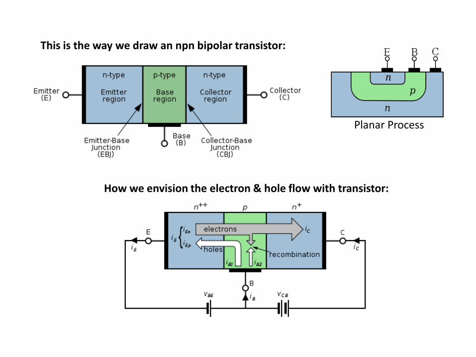
This is the way we draw an npn bipolar transistor:
How we envision the electron & hole flow with transistor:
Planar Process

Fairchild 1959 Discrete BJTs Collector contact made from the back
of die.
3-terminal TO-18
Designed by Gordon Moore

A bipolar junction transistor cross-section in a planar integrated circuit
Integrated BJTs
Collector contact made adjacent topside contact.

µA709 operational amplifier Fairchild Semiconductor – 1965
Designed by Robert Widlar
Output
In put
In put
First commercial Op Amp to became an
industry standard.

VBE
IC
IE
1BE
BE
gr
E
1( I =1 mA. = m )
26
1
EBE
TH
BE
BE
Ig
V
rg
For
NPN
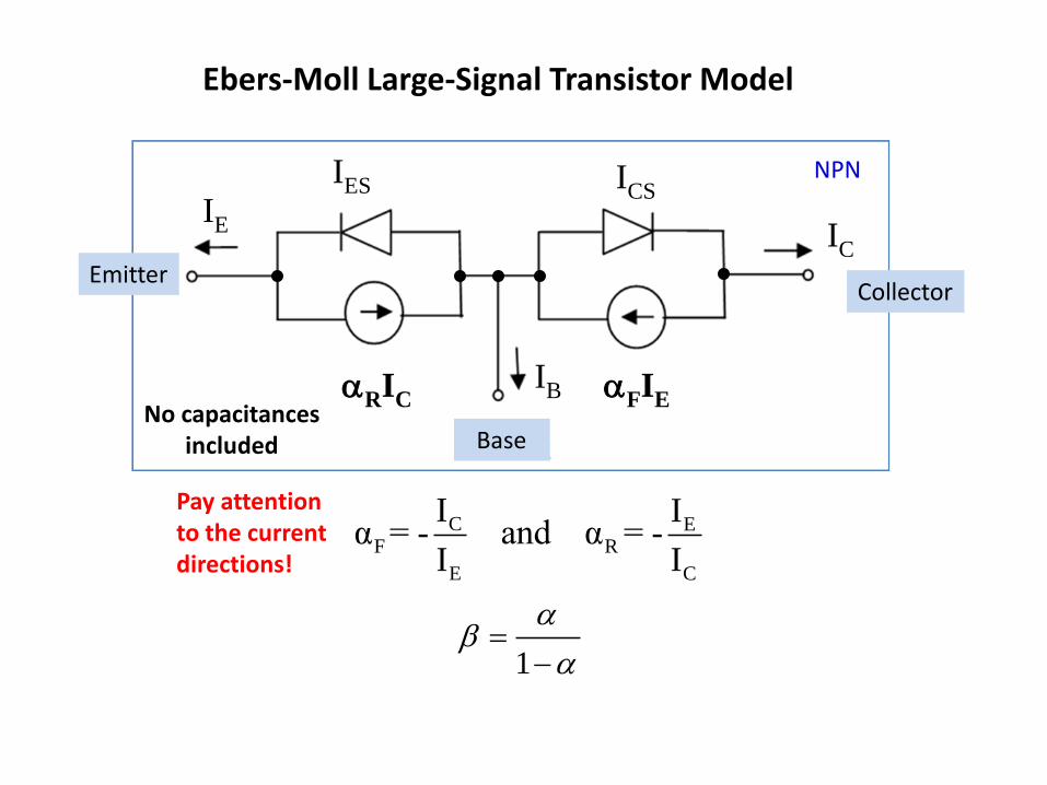
Ebers-Moll Large-Signal Transistor Model
C EF R
E C
1
I Iα = - and α = -
I I
Emitter
Base
Collector
IB
IE IC
FIE RIC No capacitances
included
NPN ICS IES
Pay attention to the current directions!

Bipolar Junction Transistor I-V Behavior in Forward Active Region
VCE
IC
Increasing VBE
Increasing IB
“Saturation” Region
VBE
IC
VBE
gm
Exponential behavior
“Forward Active” Region
NPN
No “Early Effect” shown (base width modulation)
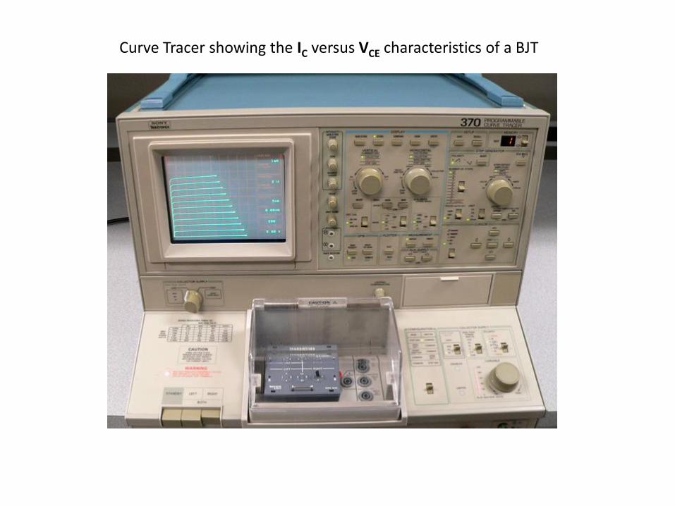
Curve Tracer showing the IC versus VCE characteristics of a BJT
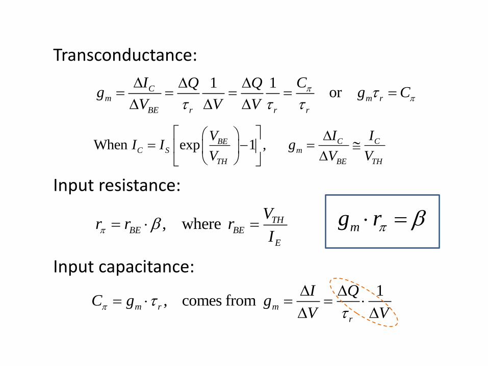
Transconductance:
Input resistance:
1 1orC
m m r
BE r r r
I CQ Qg g C
V V V
When exp 1 , C CBEC S m
TH BE TH
I IVI I g
V V V
, where THBE BE
E
Vr r r
I
Input capacitance:
mg r
1, comes fromm r m
r
I QC g g
V V

Emitter
Collector
Base
Depletion Layer
Depletion Layer
WB
Base Width
Bipolar Junction Transistor Controlled Charge and Controlling Charge Within Base Region
Origin of Ci within BJT

Forward Base Transit Time
2
2
Br
x
W
D
Log (net impurity conc)
Depth from surface 0
ND
NA
Nepi
Emitter Base Collector
WB

r C
C
rbb’
r
r0 vb’e
+
-
Hybrid- Small-Signal Model for BJT
Low-Frequency Hybrid- Small-Signal Model for BJT
Hybrid- Model
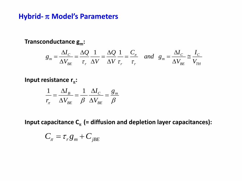
Hybrid- Model’s Parameters
1 1Cm
BE r r r
I CQ Qg and
V V V
C Cm
BE TH
I Ig
V V
Transconductance gm:
Input resistance r:
Input capacitance C (= diffusion and depletion layer capacitances):
1 1 C mB
BE BE
I gI
r V V
r m jBEC g C

EXAMPLE: Small-Signal Model Parameter Values A BJT is biased at IC = 1 mA and VCE = 3 V. =90, r =5 ps, and T = 300 K. Find (a) gm , (b) r , (c) C . Solution: (a) (b) (c)
1 mA mA/ ( / ) 39 39 mS (millisiemens)
26 mV Vm Cg I kT q
90/ 2.3 kΩ
39 mSmr g
12 145 10 0.039 1.9 10 F 19 fF (femtofarad)F mC g
From: Modern Semiconductor Devices for Integrated Circuits (C. Hu)

Hybrid- Model’s Parameters (continued)
Output resistance ro:
where is Early voltageA CEO A
C
V Vr V
I
Base spreading resistance rbb’:
Resistance from ohmic contact to the edge of the emitter
Feedback capacitance (common-emitter configuration) C:
Reverse mR jCBC g C
Feedback resistance (common-emitter configuration) r:
1 1 mRB E
CB R CB R
gI I
r V V
Typically large wrt load resistance RL
Attenuates input signal & adds noise
Limits bandwidth of CE amplifiers
Miller capacitance
Typically ignored because very large

Field-Effect Transistors (FET) or
Unipolar Transistors
JFET

Surface carrier inversion at a silicon/silicon dioxide interface

N-channel MOSFET transistor
Realistic cross-section of n-channel modern MOSFET
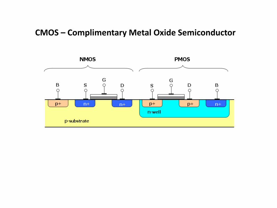
CMOS – Complimentary Metal Oxide Semiconductor

N-channel
P-channel
We will use these schematic symbols for MOSFETs