Embed Size (px)
Citation preview
1
Source Serves FMCW Radar Direct-digital-synthesizer (DDS) technology can provide the agility and frequency and phase
control needed to drive high-performance frequency-modulated-continuous-wave radar
systems.
A commercial direct-digital synthesizer was used as the linear source in an FMCW
radar system, with excellent results.
Radar sensors based on frequency-modulated-continuous-wave (FMCW) methods
benefit from high-quality signal sources. To complement FMCW radar sensors, a
frequency-agile linear-FM source with excellent spectral purity was developed using a
commercial direct-digital synthesizer (DDS) as a reference source for a wide-
bandwidth phase-locked-loop (PLL) frequency synthesizer. By employing a simple
FMCW radar architecture, it was possible to evaluate the performance of a linear-
frequency-modulated (LFM) source under closed-loop operational conditions.
Due to their architectural simplicity, FM-based radar systems are among the most
elementary types of radar equipment.1 Radar sets based on FM require a minimum
number of components compared to other radar systems and offer ease of signal
processing, owing to the narrow signal bandwidth of the received information
following frequency translation to baseband. FMCW radar sets, the most popular FM-
based sensor front-end approach, are typically employed for aircraft altimetry and
some millimeter-wave munitions and seeker applications.
The capability of FMCW radar systems to achieve high receiver sensitivity and range
resolution is directly related to the phase noise and linearity of the transmit and
receive signal sources or oscillators.2 In many cases, these sources are unitary—a
single source employing the homodyne principle. A number of different techniques
have been applied in source design to achieve good spectral purity, such as low
spurious content and low phase noise, particularly for sophisticated radar and signal
generation applications. DDS integrated-circuit (IC) devices have matured in recent
years and have shown a great deal of promise for radar applications, particularly for
the spectral purity and tuning linearity needed for FMCW radar equipment.
Unfortunately, DDS devices still suffer fundamental limitations with respect to clock
frequency, the linearity available from digital-to-analog converters (DACs), spurious-
free-dynamic-range (SFDR) performance, and tuning word memory capacity.3 To
overcome these limitations, a number of frequency synthesizer architectures have
been developed. Specifically, a DDS device in combination with PLL techniques
2
offers a simplified architecture to achieve good frequency agility and low phase
noise—the essential parameters required for FMCW radar applications.
DDS technology provides a versatile alternative to traditional frequency-agile analog
frequency synthesizer solutions. The high-density integration of the various digital
building blocks enables DDS technology to provide a frequency-agile signal source
with extraordinary capability for a wide range of applications. For many applications,
a DDS source holds significant advantages over frequency-agile analog synthesizers
based on phase-locked-loop (PLL) circuitry. The parametric advantages of a DDS
source over these analog frequency synthesizers include fine tuning resolution of
output frequency and phase; fast frequency and phase agility without overshoot or
other transient anomalies; phase-continuous frequency switching; additional circuitry
not being required for tuning, temperature, or component aging; digital interface
control being enabled by means of a modest microcontroller; the possibility of
precision amplitude and phase matching for generating quadrature signals; and the
possibility of precision, amplitude, phase, and frequency modulation.
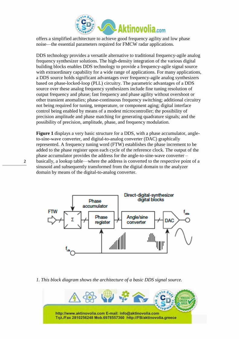
Figure 1 displays a very basic structure for a DDS, with a phase accumulator, angle-
to-sine-wave converter, and digital-to-analog converter (DAC) graphically
represented. A frequency tuning word (FTW) establishes the phase increment to be
added to the phase register upon each cycle of the reference clock. The output of the
phase accumulator provides the address for the angle-to-sine-wave converter –
basically, a lookup table—where the address is converted to the respective point of a
sinusoid and subsequently transformed from the digital domain to the analyzer
domain by means of the digital-to-analog converter.
1. This block diagram shows the architecture of a basic DDS signal source.

3
Because the data points of the output waveform are represented by digitally stored
values, the DDS defines a sampled data system with the attendant constraints—e.g.,
Nyquist sampling, output amplitude rolloff, DAC quantization noise and spurious,
and image and harmonic signals. In spite of these limitations, many of a DDS’
spectral limitations can be mitigated through the use of output filters and judicious
selections of reference clock parameters and output frequency plan.3
The output frequency of a DDS can be found from Eq. 1:
fdds = (FTW/2n)fclk (1)
where:
fdds = the DDS output frequency;
FTW = the binary frequency tuning word;
n = the number of digital bits in the frequency tuning word (typically 24 to 48 b); and
fclk = the clock frequency (in Hz).
The DDS output frequency is a fraction of the clock frequency, with resolution that
can be found by means of Eq. 2:
Δfdds = fclk/2n (2)
By way of example: For a FTW of 32 b and 1-GHz clock frequency, the DDS output
frequency resolution is 0.23 Hz. While such fine frequency resolution is rarely
needed, this capability is quite useful in reducing the spurious distortion of the output
signal.
In addition to using them as stand-alone designs, some DDS circuits can be enhanced
via integration with PLLs. The following block diagrams illustrate two DDS/PLL
configurations which may be useful in various synthesizer applications. Figure 2
shows a DDS within the feedback loop of a PLL. A prescaler divides the VCO output
frequency to the clock input frequency range of the DDS. Meanwhile, the DDS output
signal phase is compared to a high-spectral-quality reference within the phase
detector. A phase error signal is thereby created, which subsequently tunes the VCO
to the phase-locked condition.

4
2. In this block diagram, a DDS device is installed with a PLL feedback path.
The output frequency based on the frequency reference and other DDS parameters can
be found from Eq. 3:
fout = (2n/FTW)P(fref) (3)
where:
P = the division ratio of the prescaler and
fref = the frequency of the reference source.
In essence, the DDS operates as a high resolution fractional frequency divider
allowing the use of a high reference frequency and reduction of the feedback loop
modulus.
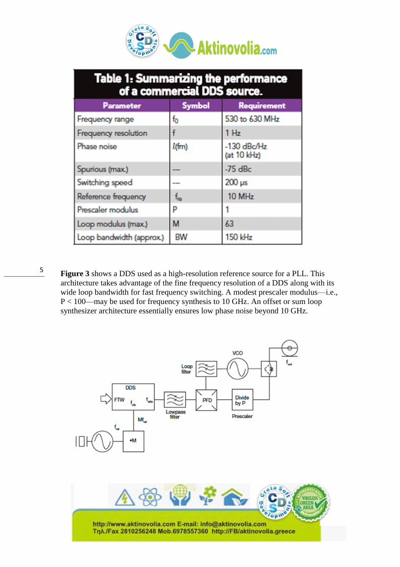
Reference 2 provides an excellent example of the performance of this synthesizer
architecture, with DDS performance summarized in Table 1.
5
Figure 3 shows a DDS used as a high-resolution reference source for a PLL. This
architecture takes advantage of the fine frequency resolution of a DDS along with its
wide loop bandwidth for fast frequency switching. A modest prescaler modulus—i.e.,
P < 100—may be used for frequency synthesis to 10 GHz. An offset or sum loop
synthesizer architecture essentially ensures low phase noise beyond 10 GHz.
6
3. This block diagram shows a DDS reference for a PLL frequency synthesizer.
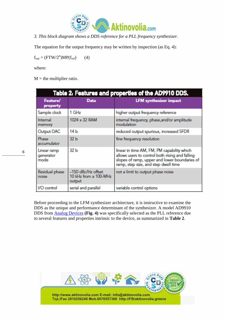
The equation for the output frequency may be written by inspection (as Eq. 4):
fout = (FTW/2n)MP(fref) (4)
where:
M = the multiplier ratio.
Before proceeding to the LFM synthesizer architecture, it is instructive to examine the
DDS as the unique and performance determinant of the synthesizer. A model AD9910
DDS from Analog Devices (Fig. 4) was specifically selected as the PLL reference due
to several features and properties intrinsic to the device, as summarized in Table 2.
7
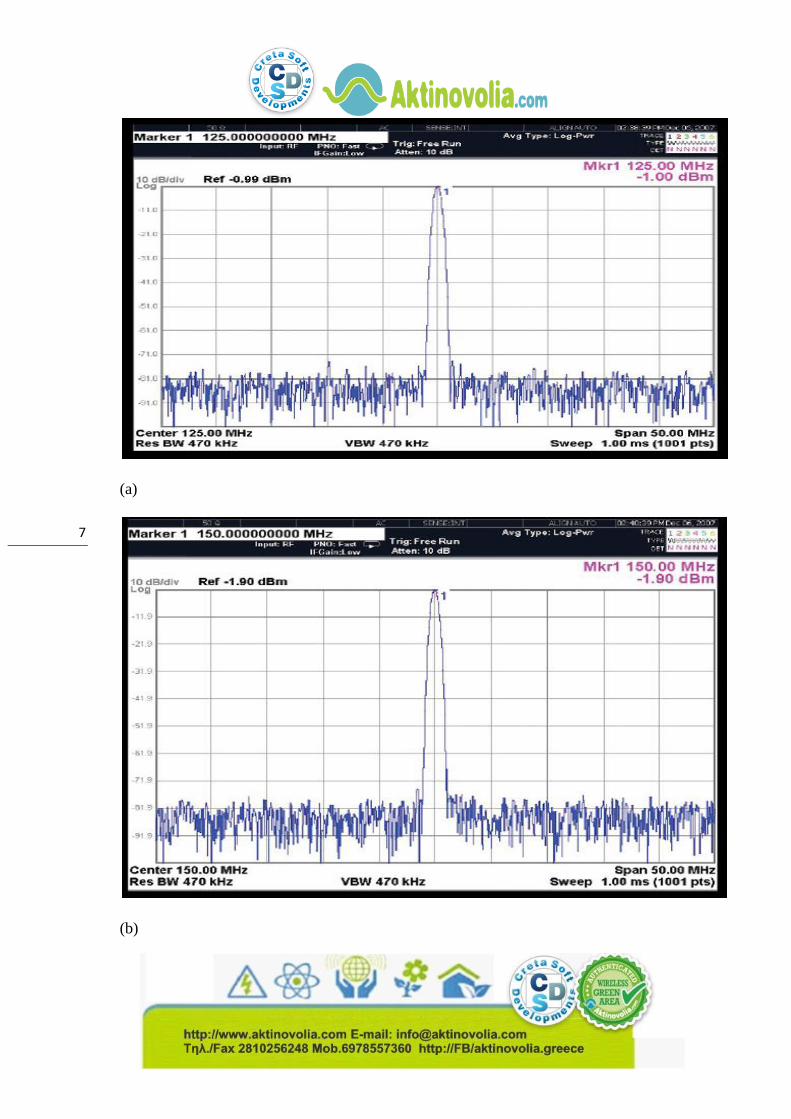
(a)
(b)
8
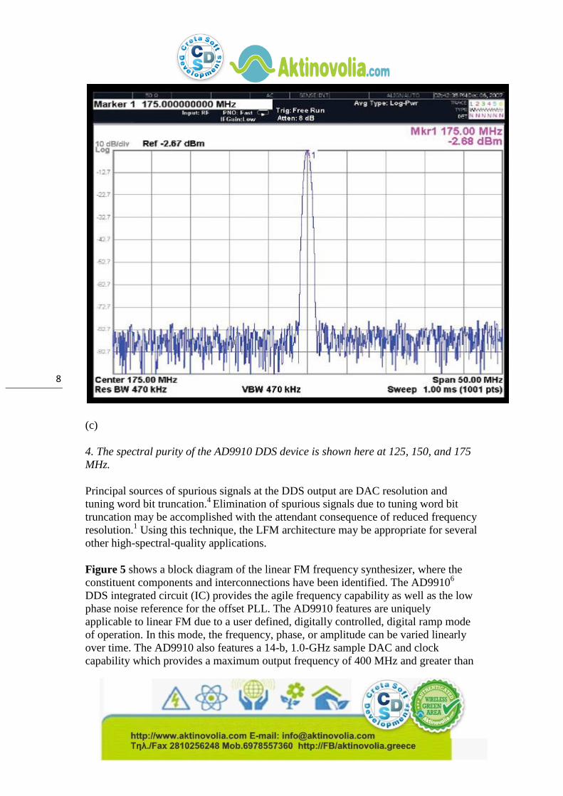
(c)
4. The spectral purity of the AD9910 DDS device is shown here at 125, 150, and 175
MHz.
Principal sources of spurious signals at the DDS output are DAC resolution and
tuning word bit truncation.4
Elimination of spurious signals due to tuning word bit
truncation may be accomplished with the attendant consequence of reduced frequency
resolution.1 Using this technique, the LFM architecture may be appropriate for several
other high-spectral-quality applications.
Figure 5 shows a block diagram of the linear FM frequency synthesizer, where the
constituent components and interconnections have been identified. The AD99106
DDS integrated circuit (IC) provides the agile frequency capability as well as the low
phase noise reference for the offset PLL. The AD9910 features are uniquely
applicable to linear FM due to a user defined, digitally controlled, digital ramp mode
of operation. In this mode, the frequency, phase, or amplitude can be varied linearly
over time. The AD9910 also features a 14-b, 1.0-GHz sample DAC and clock
capability which provides a maximum output frequency of 400 MHz and greater than
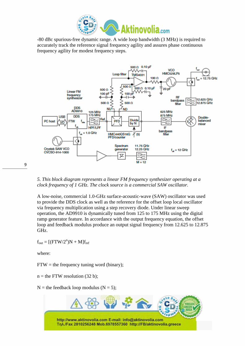
9
-80 dBc spurious-free dynamic range. A wide loop bandwidth (3 MHz) is required to
accurately track the reference signal frequency agility and assures phase continuous
frequency agility for modest frequency steps.
5. This block diagram represents a linear FM frequency synthesizer operating at a
clock frequency of 1 GHz. The clock source is a commercial SAW oscillator.
A low-noise, commercial 1.0-GHz surface-acoustic-wave (SAW) oscillator was used
to provide the DDS clock as well as the reference for the offset loop local oscillator
via frequency multiplication using a step recovery diode. Under linear sweep
operation, the AD9910 is dynamically tuned from 125 to 175 MHz using the digital
ramp generator feature. In accordance with the output frequency equation, the offset
loop and feedback modulus produce an output signal frequency from 12.625 to 12.875
GHz.
fout = [(FTW/2n)N + M]fref
where:
FTW = the frequency tuning word (binary);
n = the FTW resolution (32 b);
N = the feedback loop modulus (N = 5);

10
M = the offset loop frequency multiplier factor (M = 12); and
fclk = the clock frequency (fclk = 1.00 GHz).
The feedback loop modulus is fixed at five but could be altered to extended
synthesizer bandwidth, although this feature may require use of a switched filter bank
to reduce spurious content. The offset loop effectively reduces the feedback loop
modulus from 85 to 5, thereby lowering the phase noise by 24.5 dB within the loop
bandwidth.
The component elements of the loop filter are specifically delineated to emphasize
that accurate tracking and frequency agility of the AD9910 can only be assured with a
wideband loop; in addition, and more specifically, the loop damping must be greater
than critical—i.e., > 0.707—to prevent transient overshoot and assure asymptotic
settling.
(a)

11
(b)
6. These plots show (a) the narrowband and (b) the wideband spectra for the LMF
synthesizer.
Figure 6 represents the center frequency (12.75 GHz) spectral quality of the LFM
synthesizer under narrow and wideband conditions. The phase noise of the narrow
band spectrum (-108 dBc/Hz offset 100 kHz from the carrier) is near the phase noise
floor of the spectrum analyzer. An estimate of the phase noise from the wideband
spectrum indicates phase noise measurement (-124 dBc/Hz offset 1.0 MHz offset
frequency)—which correlates well with the phase noise estimate (-128 dBc/Hz) in
accordance with refs. 2 and 5.

12
(a)
(b)
13
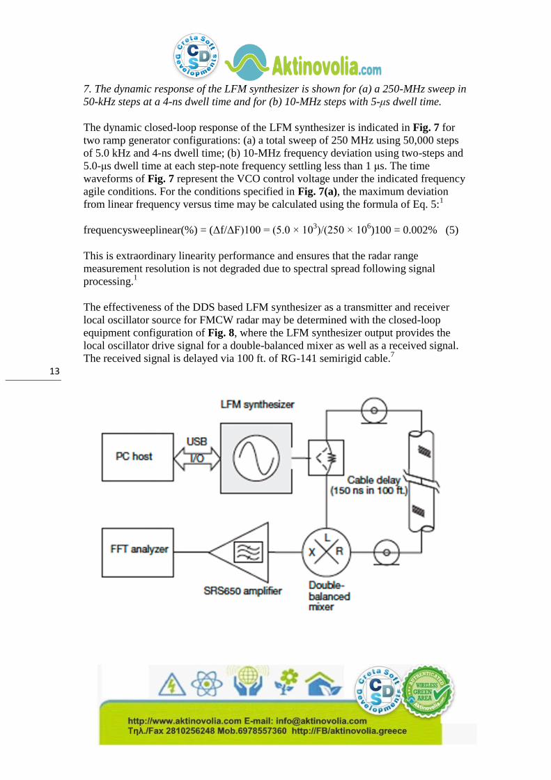
7. The dynamic response of the LFM synthesizer is shown for (a) a 250-MHz sweep in
50-kHz steps at a 4-ns dwell time and for (b) 10-MHz steps with 5-μs dwell time.
The dynamic closed-loop response of the LFM synthesizer is indicated in Fig. 7 for
two ramp generator configurations: (a) a total sweep of 250 MHz using 50,000 steps
of 5.0 kHz and 4-ns dwell time; (b) 10-MHz frequency deviation using two-steps and
5.0-μs dwell time at each step-note frequency settling less than 1 μs. The time
waveforms of Fig. 7 represent the VCO control voltage under the indicated frequency
agile conditions. For the conditions specified in Fig. 7(a), the maximum deviation
from linear frequency versus time may be calculated using the formula of Eq. 5:1
frequencysweeplinear(%) = (Δf/ΔF)100 = (5.0 × 10³)/(250 × 10
6)100 = 0.002% (5)
This is extraordinary linearity performance and ensures that the radar range
measurement resolution is not degraded due to spectral spread following signal
processing.1
The effectiveness of the DDS based LFM synthesizer as a transmitter and receiver
local oscillator source for FMCW radar may be determined with the closed-loop
equipment configuration of Fig. 8, where the LFM synthesizer output provides the
local oscillator drive signal for a double-balanced mixer as well as a received signal.
The received signal is delayed via 100 ft. of RG-141 semirigid cable.7

14
8. This diagram represents the test system for closed-loop evaluation of the LFM
synthesizer.
The IF at the mixer output can be calculated by Eq. 6:
fif = (ΔF/ΔT)τd = 3.625 kHz (6)
The equipment produces an IF signal proportional to the ramp rate and the time delay
associated with the cable. The output signal is spectrally resolved to qualitatively
determine the linearity and, possibly, the phase noise. The results of the closed-loop
test are shown in Fig. 8. Test parameters, collected from a Hamming window
analysis, include frequency deviation of 250 MHz, scan time of 0.010 s, sample rate
of 1 MSamples/s, FFT length of 10,000 points, frequency resolution of 100 Hz, range
resolution of 83 Hz/m, and cable delay of 145 ns.
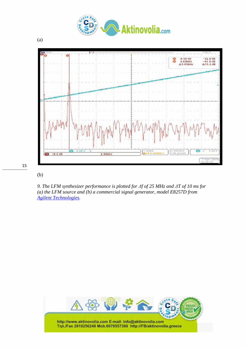
Figure 8(a) represents the IF spectrum of the LFM source and Fig. 8(b) is the IF
spectrum following substitution of the model E8257D8 signal generator as the source
for the closed-loop test. Close examination of Fig. 8 reveals higher signal-to-noise
ratio and narrower spectral width of the LFM synthesizer IF spectrum. The closed-
loop equipment functions as an FM discriminator. Therefore, the broader spectral
width of the IF signal using the E8257D signal generator is indicative of higher
residual FM noise and/or degraded linearity, since both conditions will extend the
width of the IF signal spectrum. The lower signal level in the IF spectrum of the
E8257D indicates that signal energy is distributed to adjacent frequency bins of the
spectrum.
15
(a)
(b)
9. The LFM synthesizer performance is plotted for Δf of 25 MHz and ΔT of 10 ms for
(a) the LFM source and (b) a commercial signal generator, model E8257D from
Agilent Technologies.

16
10. This photograph shows the RF section of the LFM synthesizer.
Although the test methodology is somewhat subjective, the results provide credible
evidence of the quality and suitability of the LFM synthesizer to function effectively
as a source for FMCW radar, as well as other frequency agile applications.7 Figure 9
offers a view of the RF section of the LFM synthesizer, revealing the use of discrete
and surface-mount components. Support electronics, power supply conditioning, and
control interface/functions are integrated on the lower surface (not shown). Isolation
walls and energetic grounding techniques are clearly illustrated and required to reduce
spurious signals. The source features low-loss microstrip line fabricated on RO4350
circuit substrate material from Rogers Corp. The RF section of the synthesizer is
approximately 4.0 × 4.0 × 0.5 in. (Fig. 10). To ensure adequate coupling and
isolation, attempts were not made to reduce the size of the synthesizer.
Kenneth V. Puglia, Principal
E × H Consulting Services, 146 Westview Dr., Westford, MA 01886;
(978) 692-4850, e-mail: [email protected].
17
Acknowledgments
The work reported within the article was conducted by the author while employed at
M/A-COM in 2008. The author acknowledges the diligence of Scott Crawford and
Chris Monroy in assembly, breadboard, and measurement tasks, as well as Bert
Henderson (from M/A-COM in San Jose, CA and formerly of Watkins-Johnson Co.)
for analysis, design, and prototypes of the X-band filters. The author acknowledges
and appreciates the generous and timely support of Hittite Microwave Corp.
(Chelmsform, MA); rapid acquisition of MMIC devices and evaluation boards was
significant in validation of the LFM synthesizer architecture and management of an
aggressive program schedule.
References
1. Kenneth V. Puglia, “Technical Memorandum: FMCW Radar Primer,” M/A-COM
GmbH, Schweinfurt, Germany; August 1995.
2. Keneth V. Puglia, “Technical Memorandum: Transmitter FM Noise and Frequency
Sweep Nonlinearity in FMCW Radar,” M/A-COM, GmbH, Schweinfurt, Germany,
July, 1995.
3. “Technical Tutorial on Digital Signal Synthesis,” Analog Devices, Inc., 1999,
www.analog.com.
4. Ulrich L. Rohde and Ajay Kumar Poddar, “VCSO Technology Silences
Synthesizers,” Microwaves & RF, Vol. 50, No. 2, February, 2011.
5. Kenneth V. Puglia, “Oscillator Phase Noise: Theory and Prediction,” Microwave
Journal, Vol. 50, No. 9, September, 2007, pp. 178-194.
6. Analog Devices, AD9910 data sheet, www.analog.com.
7. D. Scherer, “Design Principles and Test Methods for Low Noise RF and
Microwave Sources,” Hewlett-Packard RF and Microwave Measurement Symposium,
October, 1978.
For additional reading
H.D. Griffiths, “New Ideas in FM Radar,” Electronics and Communication
Engineering Journal, October 1990, pp. 185-194.
A.G. Stove, “Linear FMCW Radar Techniques,” IEE Proceeding-F, Vol. 139, No. 5,
October 1992, pp. 343-350.

18
J. Figueras Ventura and H. Russchenberg, “Improvement of the Performance of FM-
CW Radar Systems by using Direct Digital Synthesizers: Comparison with Voltage
Controlled Oscillators,” available via IEEE Explore.
D. Morgan, P.D.L. Beasley, K.E. Ball, and W.P. Jones, “Exploitation of direct digital
synthesis for sweep generation in FMCW radar,” ARMMS Conference, November, 7-
8, 2005, Newport Pagnell, England.
Μετα τιμής
Βλαχάκης Μιχαήλ – Επιστημονικός Συνεργάτης Cretasoft.gr Τμ.Επ. Υπολογ. Π.Κρήτης
Τηλ. 6978557360 2810256248 Email [email protected] [email protected]
BSC Φυσικομαθηματική Σχολή Π.Κρήτης