Embed Size (px)
Citation preview

1
Sources and detectors

2
Solid state detectors
Semiconductor detectors
Usually made from high purity Ge or Si single crystal containing doped layers
One side is made from p type, the other is from n type layer.
A depleted zone is created in the central region by using reverse voltage. This is the active layer.
The number of free charge carriers can be reducted by Li alloying. The Li atoms are holding thefree charge carriers of the impurities and an intrinsic layer is created.
This is called PIN diode.
Now it is possible to make high purity semiconductive materials without adding Li.

3
Solid state detectors
Due to the photoelectric effect, the incomingphotons create electron-hole pairs.
The collected charges are creating a signal on the capacitor.
The amplitude of the signal is proportional to the photon energy.
The average energy of electron-hole creation in a semiconductor (depending onthe material): δ ~ 3 – 4 eV.
The number of charges in the solid state detector is 10 times larger thanin an ionization chamber.
Therefore the statistical uncertainty is smaller and the ΔE/E energy resolutionis much better than in the case of proportional detectors. The value of theFano-factor is: F ~ 0,15.
ΔEEo
≈1−5%
Cascade mechanism: the number of chargecarriers is proportional to the number of photon.

4
Solid state detectors
The disadvantage of Li based PIN detectors (especially the Ge detektors), thata liquid N cooling (-196 Co) is needed.
The cooling stops the Li diffusion.
On the other hand, the cooling reducts further the number of free charge carriers in thedepleted zone, therefore the background and noise is further reducted.
Recently it became possible to produce extra high purity Ge and Si crystals, therefore Li is not needed anymore.
These detectors are simpler, the cooling is not needed.
The Fano-factor is even smaller, so the energy resolution is below 1%.
5
Solid state detectors
Scintillation detectors
The detectors are usually made from NaI crystal, doped by Ta atoms.
The X-ray or gamma photons indicate visible (blue) photons from the Ta positions,the number of the visible photons is proportional to the energy of the X-ray or gamma photon.
The scintillator crystal is connected to a photomultiplier tube = PMT through a lightconducting tube.
The PMT processes the visible photonswith a high efficiency.
The photons indicate electrons from the photocathode bythe photoelectric effect.
By using high voltage the electrons are accelerated and aremultiplied on the other dynodes.
The electron multiplication factor is: 104-105.
The Fano-factor is: F ~ 1
The energy resolution is worst because of the multiple step processing, than in the caseof gas filled or semiconductor detectors. The energy resolution in the case of 5-10 keV energy X-ray photons:
ΔEEo
≈50−60%
6
Solid state detectors
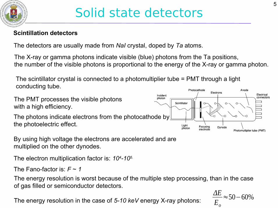
Mn Kα line detected by three different detectors:
Proportional counter: ΔE/E =15 - 20 %.
Scintillation detector: ΔE/E =50 - 60 %.
The resolution in the case of 5 -10 keV energy:
Solid state detector ΔE/E =1 - 5 %.

7
Multi-channel analysator
Multi-channel analizer analysator = MCA
It sorts the incoming impulses based on the amplitude of the signal. It is a histogram creating device.
The incoming analog impulses are digitalized and the number of impulses isincreased by one in the channel corresponding to the amplitude of the signal.
8
Imaging detectors
Older imaging detectors:
• Silver bromid (AgBr) plated film for off-line detection• ZnS mixed by Ni is fluorescent. X-ray or gamma photons indicate green light. for on-line observation.
Newer devices for 2D detection:
• CCD (Charge coupled device)• Imaging plate
9
Imaging detectors
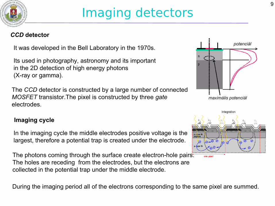
CCD detector
It was developed in the Bell Laboratory in the 1970s.
Its used in photography, astronomy and its importantin the 2D detection of high energy photons(X-ray or gamma).
The CCD detector is constructed by a large number of connectedMOSFET transistor.The pixel is constructed by three gateelectrodes.
In the imaging cycle the middle electrodes positive voltage is thelargest, therefore a potential trap is created under the electrode.
The photons coming through the surface create electron-hole pairs.The holes are receding from the electrodes, but the electrons arecollected in the potential trap under the middle electrode.
During the imaging period all of the electrons corresponding to the same pixel are summed.
Imaging cycle

10
Imaging detectors
pixe
l bo
unda
ry
Charge packetp-type silicon
n-type silicon
SiO2 Insulating layer
Electrode Structure
pixe
l bo
unda
ry
inco
min
gph
oto
ns
Imaging cycle

1
2
3
+5V
0V
-5V
+5V
0V
-5V
+5V
0V
-5V
1
2
3
11
Imaging detectors
Readout cycle
1
2
3
+5V
0V
-5V
+5V
0V
-5V
+5V
0V
-5V
1
2
3
12
Imaging detectors
Readout cycle
1
2
3
+5V
0V
-5V
+5V
0V
-5V
+5V
0V
-5V
1
2
3
13
Imaging detectors
Readout cycle

1
2
3
+5V
0V
-5V
+5V
0V
-5V
+5V
0V
-5V
1
2
3
14
Imaging detectors
Readout cycle

1
2
3
+5V
0V
-5V
+5V
0V
-5V
+5V
0V
-5V
1
2
3
15
Imaging detectors
Readout cycle

16
Imaging detectors
Readout cycle
1
2
3
+5V
0V
-5V
+5V
0V
-5V
+5V
0V
-5V
1
2
3

17
Imaging detectors
Readout cycle
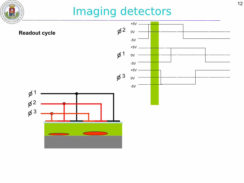
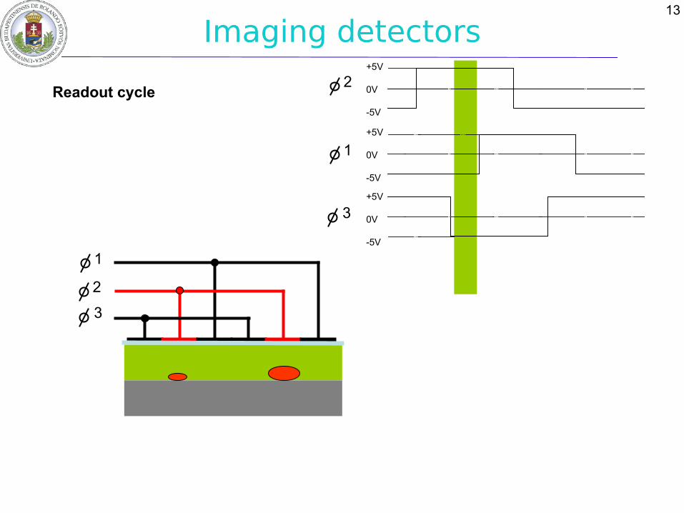
The voltage of the subsequent electrodes are changed step bystep, so that the charges collected by the pixels are movingtowards the end of the row.
At the end of the row the readout electrode is reading outthe charge collected by each pixel.
The electronics connected to the readout electrode creates the 2D image.
The largest CCD detector installed on a single wafer:In 2008~ 15 cm x 15 cm surfaceIn 2011 ~ 20 cm x 20 cm surface (16 Mpixel resolution).
X-ray CCD detector
18
Imaging detectors
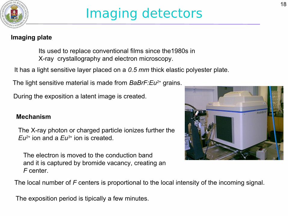
Imaging plate
Its used to replace conventional films since the1980s inX-ray crystallography and electron microscopy.
It has a light sensitive layer placed on a 0.5 mm thick elastic polyester plate.
The light sensitive material is made from BaBrF:Eu2+ grains.
During the exposition a latent image is created.
Mechanism
The X-ray photon or charged particle ionizes further theEu2+ ion and a Eu3+ ion is created.
The electron is moved to the conduction bandand it is captured by bromide vacancy, creating anF center.
The local number of F centers is proportional to the local intensity of the incoming signal.
The exposition period is tipically a few minutes.

19
Imaging detectors
The surface of the plate is scanned by a focussed He-Ne laserbeam (red light, 633 nm) with and approx. 100 μm diameter.
Readout
The electrons freed from the F centrums are transformingback the Eu3+ ions to Eu2+ ions together with blue light emission.
An optical system scanning the surface together the laser beamis collecting the photons.
The signal is amplified by a photomultiplier and after digitalizationthe computer is transforming the data to a 2D image.
After readout the system is homogenized by white light.

20
Imaging detectors
Properties of the system
The image is conserved for a long period without readout (the half-lifeis approx. 10 hours).
The resolution is approx. 150 μm x 150 μm
The maximal possible surface is much larger than in thecase of the CCD detectors.
The highest resolution: 6000 x 5000 pixel.
Its advantage is that the digital data are transferred tothe computer in a relatively simple way.
Policrystalline diffraction image recorded byimaging plate