Embed Size (px)
Citation preview
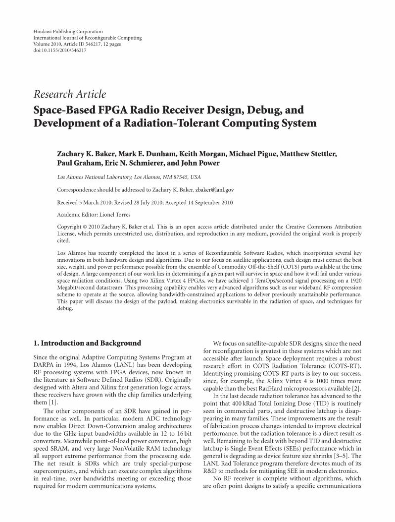
Hindawi Publishing CorporationInternational Journal of Reconfigurable ComputingVolume 2010, Article ID 546217, 12 pagesdoi:10.1155/2010/546217
Research Article
Space-Based FPGA Radio Receiver Design, Debug, andDevelopment of a Radiation-Tolerant Computing System
Zachary K. Baker, Mark E. Dunham, Keith Morgan, Michael Pigue, Matthew Stettler,Paul Graham, Eric N. Schmierer, and John Power
Los Alamos National Laboratory, Los Alamos, NM 87545, USA
Correspondence should be addressed to Zachary K. Baker, [email protected]
Received 5 March 2010; Revised 28 July 2010; Accepted 14 September 2010
Academic Editor: Lionel Torres
Copyright © 2010 Zachary K. Baker et al. This is an open access article distributed under the Creative Commons AttributionLicense, which permits unrestricted use, distribution, and reproduction in any medium, provided the original work is properlycited.
Los Alamos has recently completed the latest in a series of Reconfigurable Software Radios, which incorporates several keyinnovations in both hardware design and algorithms. Due to our focus on satellite applications, each design must extract the bestsize, weight, and power performance possible from the ensemble of Commodity Off-the-Shelf (COTS) parts available at the timeof design. A large component of our work lies in determining if a given part will survive in space and how it will fail under variousspace radiation conditions. Using two Xilinx Virtex 4 FPGAs, we have achieved 1 TeraOps/second signal processing on a 1920Megabit/second datastream. This processing capability enables very advanced algorithms such as our wideband RF compressionscheme to operate at the source, allowing bandwidth-constrained applications to deliver previously unattainable performance.This paper will discuss the design of the payload, making electronics survivable in the radiation of space, and techniques fordebug.
1. Introduction and Background
Since the original Adaptive Computing Systems Program atDARPA in 1994, Los Alamos (LANL) has been developingRF processing systems with FPGA devices, now known inthe literature as Software Defined Radios (SDR). Originallydesigned with Altera and Xilinx first generation logic arrays,these receivers have grown with the chip families underlyingthem [1].
The other components of an SDR have gained in per-formance as well. In particular, modern ADC technologynow enables Direct Down-Conversion analog architecturesdue to the GHz input bandwidths available in 12 to 16 bitconverters. Meanwhile point-of-load power conversion, highspeed SRAM, and very large NonVolatile RAM technologyall support extreme performance from the processing side.The net result is SDRs which are truly special-purposesupercomputers, and which can execute complex algorithmsin real-time, over bandwidths meeting or exceeding thoserequired for modern communications systems.
We focus on satellite-capable SDR designs, since the needfor reconfiguration is greatest in these systems which are notaccessible after launch. Space deployment requires a robustresearch effort in COTS Radiation Tolerance (COTS-RT).Identifying promising COTS-RT parts is key to our success,since, for example, the Xilinx Virtex 4 is 1000 times morecapable than the best RadHard microprocessors available [2].
In the last decade radiation tolerance has advanced to thepoint that 400 kRad Total Ionizing Dose (TID) is routinelyseen in commercial parts, and destructive latchup is disap-pearing in many families. These improvements are the resultof fabrication process changes intended to improve electricalperformance, but the radiation tolerance is a direct result aswell. Remaining to be dealt with beyond TID and destructivelatchup is Single Event Effects (SEEs) performance which ingeneral is degrading as device feature size shrinks [3–5]. TheLANL Rad Tolerance program therefore devotes much of itsR&D to methods for mitigating SEE in modern electronics.
No RF receiver is complete without algorithms, whichare often point designs to satisfy a specific communications
2 International Journal of Reconfigurable Computing
Classic superheterodyne receiver
RF amp Mixer
Localoscillator
Bandpass filterIF
ampVideoADC
150 MHzinput BW
(a)
New direct conversion receiver
RF amp Bandpass filter RFamp
RFADC
∼1 GHzinput BW
(b)
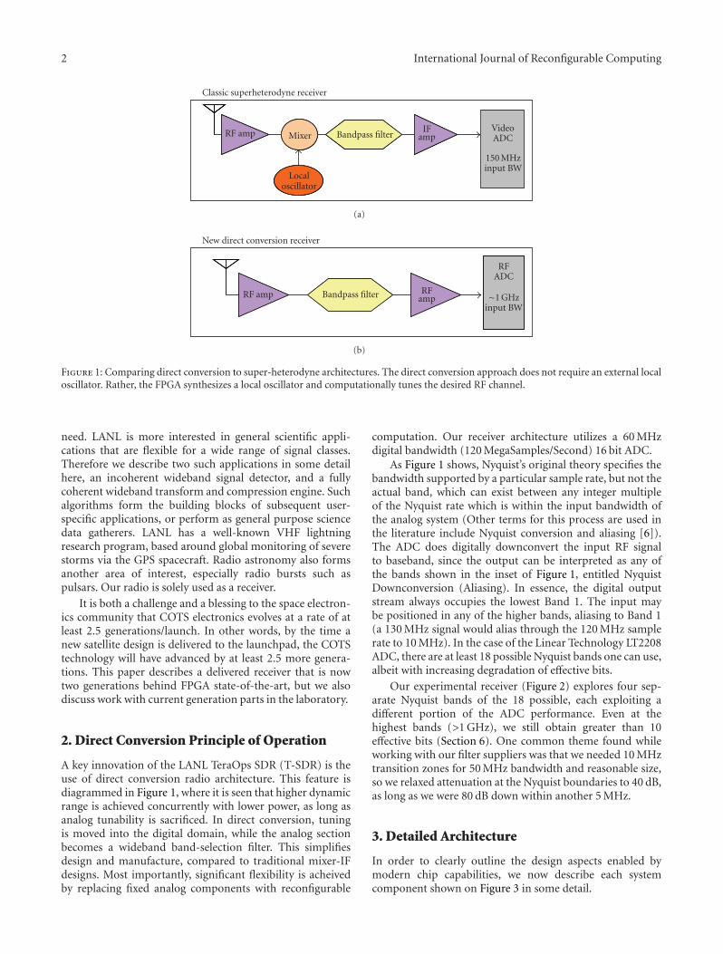
Figure 1: Comparing direct conversion to super-heterodyne architectures. The direct conversion approach does not require an external localoscillator. Rather, the FPGA synthesizes a local oscillator and computationally tunes the desired RF channel.
need. LANL is more interested in general scientific appli-cations that are flexible for a wide range of signal classes.Therefore we describe two such applications in some detailhere, an incoherent wideband signal detector, and a fullycoherent wideband transform and compression engine. Suchalgorithms form the building blocks of subsequent user-specific applications, or perform as general purpose sciencedata gatherers. LANL has a well-known VHF lightningresearch program, based around global monitoring of severestorms via the GPS spacecraft. Radio astronomy also formsanother area of interest, especially radio bursts such aspulsars. Our radio is solely used as a receiver.
It is both a challenge and a blessing to the space electron-ics community that COTS electronics evolves at a rate of atleast 2.5 generations/launch. In other words, by the time anew satellite design is delivered to the launchpad, the COTStechnology will have advanced by at least 2.5 more genera-tions. This paper describes a delivered receiver that is nowtwo generations behind FPGA state-of-the-art, but we alsodiscuss work with current generation parts in the laboratory.
2. Direct Conversion Principle of Operation
A key innovation of the LANL TeraOps SDR (T-SDR) is theuse of direct conversion radio architecture. This feature isdiagrammed in Figure 1, where it is seen that higher dynamicrange is achieved concurrently with lower power, as long asanalog tunability is sacrificed. In direct conversion, tuningis moved into the digital domain, while the analog sectionbecomes a wideband band-selection filter. This simplifiesdesign and manufacture, compared to traditional mixer-IFdesigns. Most importantly, significant flexibility is acheivedby replacing fixed analog components with reconfigurable
computation. Our receiver architecture utilizes a 60 MHzdigital bandwidth (120 MegaSamples/Second) 16 bit ADC.
As Figure 1 shows, Nyquist’s original theory specifies thebandwidth supported by a particular sample rate, but not theactual band, which can exist between any integer multipleof the Nyquist rate which is within the input bandwidth ofthe analog system (Other terms for this process are used inthe literature include Nyquist conversion and aliasing [6]).The ADC does digitally downconvert the input RF signalto baseband, since the output can be interpreted as any ofthe bands shown in the inset of Figure 1, entitled NyquistDownconversion (Aliasing). In essence, the digital outputstream always occupies the lowest Band 1. The input maybe positioned in any of the higher bands, aliasing to Band 1(a 130 MHz signal would alias through the 120 MHz samplerate to 10 MHz). In the case of the Linear Technology LT2208ADC, there are at least 18 possible Nyquist bands one can use,albeit with increasing degradation of effective bits.
Our experimental receiver (Figure 2) explores four sep-arate Nyquist bands of the 18 possible, each exploiting adifferent portion of the ADC performance. Even at thehighest bands (>1 GHz), we still obtain greater than 10effective bits (Section 6). One common theme found whileworking with our filter suppliers was that we needed 10 MHztransition zones for 50 MHz bandwidth and reasonable size,so we relaxed attenuation at the Nyquist boundaries to 40 dB,as long as we were 80 dB down within another 5 MHz.
3. Detailed Architecture
In order to clearly outline the design aspects enabled bymodern chip capabilities, we now describe each systemcomponent shown on Figure 3 in some detail.
International Journal of Reconfigurable Computing 3
DCRbandfilters
LTC 2208ADC &
RF switchmatrix
Clockmultiplier:20 → 120
MHz
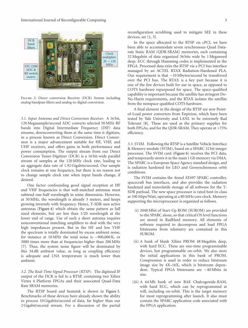
Figure 2: Direct conversion Receiver (DCR) System includinganalog bandpass filters and analog-to-digital conversion.
3.1. Input Antenna and Direct Conversion Receiver. A 16 bit,120 Megasample/second ADC converts selected 50 MHz RFbands into Digital Intermediate Frequency (DIF) datastreams, downconverting them at the same time it digitizes,in a process known as Direct Conversion. Direct Conver-sion is a major advancement suitable for HF, VHF, andUHF receivers, and offers gains in both performance andpower consumption. The output stream from our DirectConversion Tuner-Digitizer (DCR) is a 16 bit-wide parallelstream of samples at the 120 MHz clock rate, leading toan aggregate data rate of 1.92 Gigabits/second. Our sampleclock remains at one frequency, but there is no reason notto change sample clock rate when input bands change, ifdesired.
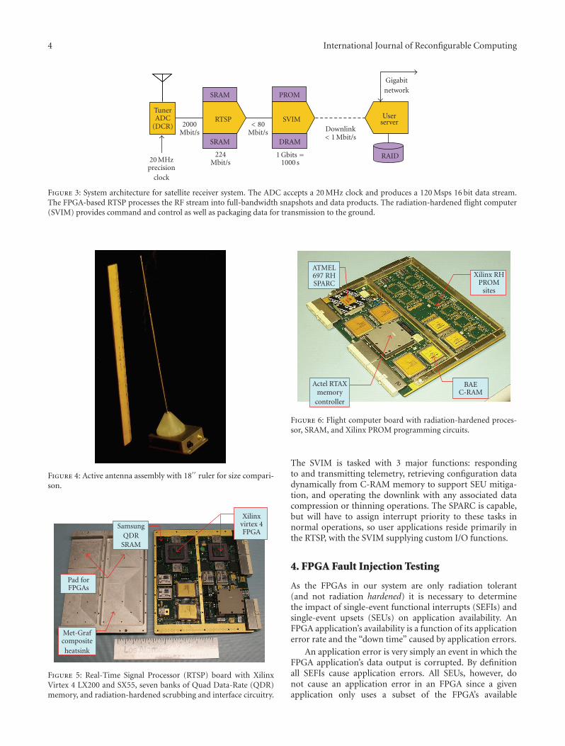
One factor confounding good signal reception at HFand VHF frequencies is that well-matched antennas mustsubtend one-half wavelength in some dimension. However,at 50 MHz, the wavelength is already 3 meters, and keepsgrowing inversely with frequency. Hence, T-SDR uses activeantennas (Figure 4) which obtain the same pattern as fullsized elements, but are less than 1/20 wavelength at thelower end of range. Use of such a short antenna requiresnonconventional matching amplifiers to deal with the veryhigh impedances present. But in the HF and low VHFthe spectrum is totally dominated by excess ambient noise,for instance at 10 MHz the total noise is ∼900,000 K, or3000 times more than at frequencies higher than 200 MHz[7]. Thus, the system noise figure will be dominated bythis 34 dB ambient value, as long as coupling efficiencyis adequate and LNA temperature is much lower thanambient.
3.2. The Real-Time Signal Processor (RTSP). The digitized IFoutput of the DCR is fed to a RTSP, containing two XilinxVirtex 4 Platform FPGAs and their associated Quad-DataRate SRAM memories.
The RTSP board and heatsink is shown in Figure 5.Benchmarks of these devices have already shown the abilityto process 10 Gigabits/second of data, far higher than our2 Gigabit/second stream. For a discussion of the partial
reconfiguration scrubbing used to mitigate SEE in thesedevices, see [1, 3].
In the space allocated to the RTSP on cPCI, we havebeen able to accommodate seven synchronous Quad Data-rate Static RAM (QDR-SRAM) memories, each containing32 Megabits of data organized 36 bits wide by 1 Megaworddeep. ECC through Hamming codes is implemented in theFPGA. Processed data exits the RTSP via a PCI bus interfacemanaged by an ACTEL RTAX Radiation-Hardened PLA.Our requirement is that ∼10 Mbytes/second be transferredover the PCI bus. The RTAX is a key part because it isone of the few devices built for use in space, as opposed toCOTS hardware repurposed for space. The space-qualifiedcapability is important because the satellite has stringent Do-No-Harm requirements, and the RTAX isolates the satellitefrom the nonspace-qualified COTS hardware.
A final element in the design of the RTSP are new Point-of-Load power converters from Enpirion, which have beentested by Yale University and LANL to be extremely RadTolerant [8]. These are used as the primary supplies forboth FPGAs, and for the QDR-SRAM. They operate at >75%efficiency.
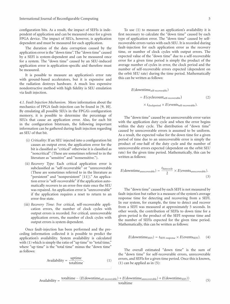
3.3. SVIM. Following the RTSP is a Satellite Vehicle Interface& Memory module (SVIM), based on a SPARC 32 bit integerprocessor. The SVIM card (Figure 6) receives the PCI data,and temporarily stores it in the main 1 Gb memory via DMA.The SPARC is a European Space Agency standard design, andis radiation hardened for LEO and Geosynchronous orbitconditions.
The SVIM contains the Atmel AT697 SPARC controller,spacecraft bus interfaces, and also provides the radiationhardened and nonvolatile storage of all software for the T-SDR payload. The new space processor is rated best-in-classat 100 Mips/Watt, operating at a 80 MHz core clock. Memorysupporting the microprocessor is organized as follows.
(i) 2048 Mbit of Start-Up ROM (SUROM) are providedto the SPARC alone, so that critical OS level functionsare stored in RadHard memory. All elements ofsoftware required to decompress and load FPGAbitstreams from telemetry are contained in thisSUROM.
(ii) A bank of blank Xilinx PROM 48 Megabits deep,with hard ECC. These are one-time programmabledevices, but programmable on-orbit. We also storethe initial applications in this bank of PROM.Compression is used in order to reduce bitstreamimage size by 4X–16X, which is bitstream depen-dent. Typical FPGA bitstreams are ∼40 Mbits insize.
(iii) A 64 Mb bank of new BAE Chalcogenide-RAM,with hard ECC, which can be reprogrammed atwill, including on-orbit. This is the target memoryfor most reprogramming after launch. It also mustcontain the SPARC application code associated withthe FPGA application.
4 International Journal of Reconfigurable Computing
TunerADC
(DCR)
20 MHzprecision
clock
SRAM
RTSP
SRAM
2000Mbit/s
224Mbit/s
< 80Mbit/s
PROM
SVIM
DRAM
1 Gbits =1000 s
Downlink< 1 Mbit/s
Gigabitnetwork
Userserver
RAID
Figure 3: System architecture for satellite receiver system. The ADC accepts a 20 MHz clock and produces a 120 Msps 16 bit data stream.The FPGA-based RTSP processes the RF stream into full-bandwidth snapshots and data products. The radiation-hardened flight computer(SVIM) provides command and control as well as packaging data for transmission to the ground.
Figure 4: Active antenna assembly with 18′′ ruler for size compari-son.
SamsungQDR
SRAM
Pad forFPGAs
Met-Grafcompositeheatsink
Xilinxvirtex 4FPGA
Figure 5: Real-Time Signal Processor (RTSP) board with XilinxVirtex 4 LX200 and SX55, seven banks of Quad Data-Rate (QDR)memory, and radiation-hardened scrubbing and interface circuitry.
ATMEL697 RHSPARC
Actel RTAXmemory
controller
BAEC-RAM
Xilinx RHPROM
sites
Figure 6: Flight computer board with radiation-hardened proces-sor, SRAM, and Xilinx PROM programming circuits.
The SVIM is tasked with 3 major functions: respondingto and transmitting telemetry, retrieving configuration datadynamically from C-RAM memory to support SEU mitiga-tion, and operating the downlink with any associated datacompression or thinning operations. The SPARC is capable,but will have to assign interrupt priority to these tasks innormal operations, so user applications reside primarily inthe RTSP, with the SVIM supplying custom I/O functions.
4. FPGA Fault Injection Testing
As the FPGAs in our system are only radiation tolerant(and not radiation hardened) it is necessary to determinethe impact of single-event functional interrupts (SEFIs) andsingle-event upsets (SEUs) on application availability. AnFPGA application’s availability is a function of its applicationerror rate and the “down time” caused by application errors.
An application error is very simply an event in which theFPGA application’s data output is corrupted. By definitionall SEFIs cause application errors. All SEUs, however, donot cause an application error in an FPGA since a givenapplication only uses a subset of the FPGA’s available
International Journal of Reconfigurable Computing 5
configuration bits. As a result, the impact of SEFIs is inde-pendent of application and can be measured once for a givenFPGA device. The impact of SEUs, however, is applicationdependent and must be measured for each application.
The duration of the data corruption caused by theapplication error is the “down time”. The “down time” causedby a SEFI is system-dependent and can be measured oncefor a system. The “down time” caused by an SEU-inducedapplication error is application-specific and therefore mustbe measured.
It is possible to measure an application’s error ratewith ground-based accelerators, but it is expensive andthe radiation destroys hardware. A much less expensivenondestructive method with high fidelity is SEU emulationvia fault injection.
4.1. Fault Injection Mechanism. More information about themechanics of FPGA fault-injection can be found in [9, 10].By emulating all possible SEUs in the FPGA’s configurationmemory, it is possible to determine the percentage ofSEUs that cause an application error. Also, for each bitin the configuration bitstream, the following importantinformation can be gathered during fault injection regardingan SEU of that bit.
(i) Criticality: If an SEU injected into a configuration bitcauses an output error, the application error for thebit is classified as “critical” otherwise it is classified as“noncritical” (These are sometimes referred to in theliterature as “sensitive” and “nonsensitive.”).
(ii) Recovery Type: Each critical application error issubclassified as “self-recoverable” or “unrecoverable(These are sometimes referred to in the literature as“persistent” and “nonpersistent” [11]).” An applica-tion error is “self-recoverable” if the application auto-matically recovers to an error-free state once the SEUwas repaired. An application error is “unrecoverable”if the application requires a reset to return to anerror-free state.
(iii) Recovery Time: For critical, self-recoverable appli-cation errors, the number of clock cycles withoutput errors is recorded. For critical, unrecoverableapplication errors, the number of clock cycles withoutput errors is system dependent.
Once fault-injection has been performed and the pre-ceding information collected it is possible to predict theapplication’s availability. System availability is calculatedwith (1) which is simply the ratio of “up time” to “total time,”where “up time” is the “total time” minus the “down time”as follows:
Availability = uptimetotaltime
. (1)
To use (1) to measure an application’s availability it isfirst necessary to calculate the “down time” caused by eachtype of application error. The “down time” caused by self-recoverable errors varies with each SEU. It is recorded duringfault-injection for each application error as the recoverytime, or number of clock cycles with output errors. Theexpected value of the “down time” due to a self-recoverableerror for a given time period is simply the product of theaverage number of cycles in error, the clock period and thenumber of self-recoverable errors expected (dependent onthe orbit SEU rate) during the time period. Mathematicallythis can be written as follows:
E(downtimeself-recoverable)
= E(cyclecountself-recoverable
)
× tclockperiod × E(eventsself-recoverable).
(2)
The “down time” caused by an unrecoverable error varieswith the application duty cycle and when the error beginswithin the duty cycle. The distribution of “down time”caused by unrecoverable errors is assumed to be uniform.As a result, the expected value for the down time for a givenperiod of time due to an unrecoverable error is simply theproduct of one-half of the duty cycle and the number ofunrecoverable errors expected (dependent on the orbit SEUrate) for the given time period. Mathematically, this can bewritten as follows:
E(downtimeunrecoverable) = tdutycycle
2× E(eventsunrecoverable).
(3)
The “down time” caused by each SEFI is not measured byfault-injection but rather is a measure of the system’s averageresponse time for detecting and recovering from a SEFI.In our system, for example, the time to detect and recoverfrom a SEFI was measured at approximately 5 seconds. Inother words, the contribution of SEFIs to down time for agiven period is the product of the SEFI response time andthe number of SEFIs expected for the given time period.Mathematically, this can be written as follows:
E(downtimeSEFI) = tSEFI-response × E(eventsSEFI). (4)
The overall estimated “down time” is the sum ofthe “down time” for self-recoverable errors, unrecoverableerrors, and SEFIs for a given time period. Once this is known,(1) can be applied as in (5):
Availability = totaltime− (E(downtimeself-recoverable) + E(downtimeunrecoverable) + E(downtimeSEFI))totaltime
. (5)
6 International Journal of Reconfigurable Computing
HDL design
HDL synthesis
Automateddesign hardening
FPGA implementation
Design verification(including hardness
assurancethrough fault injection and
design analysis)
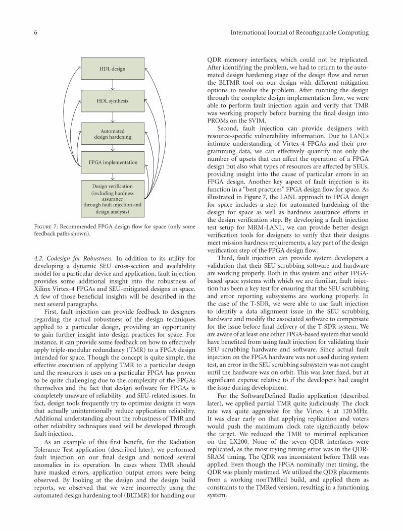
Figure 7: Recommended FPGA design flow for space (only somefeedback paths shown).
4.2. Codesign for Robustness. In addition to its utility fordeveloping a dynamic SEU cross-section and availabilitymodel for a particular device and application, fault injectionprovides some additional insight into the robustness ofXilinx Virtex-4 FPGAs and SEU-mitigated designs in space.A few of those beneficial insights will be described in thenext several paragraphs.
First, fault injection can provide feedback to designersregarding the actual robustness of the design techniquesapplied to a particular design, providing an opportunityto gain further insight into design practices for space. Forinstance, it can provide some feedback on how to effectivelyapply triple-modular redundancy (TMR) to a FPGA designintended for space. Though the concept is quite simple, theeffective execution of applying TMR to a particular designand the resources it uses on a particular FPGA has provento be quite challenging due to the complexity of the FPGAsthemselves and the fact that design software for FPGAs iscompletely unaware of reliability- and SEU-related issues. Infact, design tools frequently try to optimize designs in waysthat actually unintentionally reduce application reliability.Additional understanding about the robustness of TMR andother reliability techniques used will be developed throughfault injection.
As an example of this first benefit, for the RadiationTolerance Test application (described later), we performedfault injection on our final design and noticed severalanomalies in its operation. In cases where TMR shouldhave masked errors, application output errors were beingobserved. By looking at the design and the design buildreports, we observed that we were incorrectly using theautomated design hardening tool (BLTMR) for handling our
QDR memory interfaces, which could not be triplicated.After identifying the problem, we had to return to the auto-mated design hardening stage of the design flow and rerunthe BLTMR tool on our design with different mitigationoptions to resolve the problem. After running the designthrough the complete design implementation flow, we wereable to perform fault injection again and verify that TMRwas working properly before burning the final design intoPROMs on the SVIM.
Second, fault injection can provide designers withresource-specific vulnerability information. Due to LANLsintimate understanding of Virtex-4 FPGAs and their pro-gramming data, we can effectively quantify not only thenumber of upsets that can affect the operation of a FPGAdesign but also what types of resources are affected by SEUs,providing insight into the cause of particular errors in anFPGA design. Another key aspect of fault injection is itsfunction in a “best practices” FPGA design flow for space. Asillustrated in Figure 7, the LANL approach to FPGA designfor space includes a step for automated hardening of thedesign for space as well as hardness assurance efforts inthe design verification step. By developing a fault injectiontest setup for MRM-LANL, we can provide better designverification tools for designers to verify that their designsmeet mission hardness requirements, a key part of the designverification step of the FPGA design flow.
Third, fault injection can provide system developers avalidation that their SEU scrubbing software and hardwareare working properly. Both in this system and other FPGA-based space systems with which we are familiar, fault injec-tion has been a key test for ensuring that the SEU scrubbingand error reporting subsystems are working properly. Inthe case of the T-SDR, we were able to use fault injectionto identify a data alignment issue in the SEU scrubbinghardware and modify the associated software to compensatefor the issue before final delivery of the T-SDR system. Weare aware of at least one other FPGA-based system that wouldhave benefited from using fault injection for validating theirSEU scrubbing hardware and software. Since actual faultinjection on the FPGA hardware was not used during systemtest, an error in the SEU scrubbing subsystem was not caughtuntil the hardware was on orbit. This was later fixed, but atsignificant expense relative to if the developers had caughtthe issue during development.
For the SoftwareDefined Radio application (describedlater), we applied partial TMR quite judiciously. The clockrate was quite aggressive for the Virtex 4 at 120 MHz.It was clear early on that applying replication and voterswould push the maximum clock rate significantly belowthe target. We reduced the TMR to minimal replicationon the LX200. None of the seven QDR interfaces werereplicated, as the most trying timing error was in the QDR-SRAM timing. The QDR was inconsistent before TMR wasapplied. Even though the FPGA nominally met timing, theQDR was plainly mistimed. We utilized the QDR placementsfrom a working nonTMRed build, and applied them asconstraints to the TMRed version, resulting in a functioningsystem.
International Journal of Reconfigurable Computing 7
5. Introduction to In Situ Debug
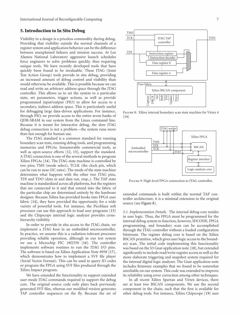
Visibility in a design is a priceless commodity during debug.Providing that visibility outside the normal channels of aregister system and application behavior can be the differencebetween unexplained failures and mission success. At LosAlamos National Laboratory aggressive launch schedulesforce engineers to solve problems quickly, thus requiringunique tools. We have recently developed tools that havequickly been found to be invaluable. These JTAG (JointTest Action Group) tools provide in situ debug, providingan increased amount of debug control and visibility thanwould otherwise be available. This is possible because we canread and write an arbitrary address space through the JTAGcontroller. This allows us to set the system to a particularstate, set parameters, trigger actions, as well as provideprogrammed input/output (PIO) to allow for access to asecondary, indirect address space. This is particularly usefulfor debugging large data-driven applications. For instance,through PIO, we provide access to the entire seven banks ofQDR-SRAM in our system from the Linux command line.Because it is meant for interactive debug, the slow JTAGdebug connection is not a problem—the system runs morethan fast enough for human use.
The JTAG standard is a common standard for runningboundary scan tests, running debug tools, and programmingmemories and FPGAs. Innumerable commercial tools, aswell as open-source efforts [12, 13], support the standard.A JTAG connection is one of the several methods to programXilinx FPGAs [14]. The JTAG state machine is controlled bytwo pins; TMS (mode select), TCLK (the clock pin, whichcan be run to near-DC rates). The mode of the state machinedetermines what happens with the other two JTAG pins,TDI and TDO (data in and data out, resp.,). The TAP statemachine is standardized across all platforms, but the registersthat are connected to it and that extend into the fabric ofthe particular chip are determined entirely by the hardwaredesigner. Because Xilinx has provided hooks into FPGA userfabric [14], they have provided the opportunity for a widevariety of powerful tools. For instance, the Picoblaze softprocessor can use this approach to load user programs [15]and the Chipscope internal logic analyzer provides cross-hierarchy visibility.
In order to provide in situ access to the JTAG chain, weimplement a JTAG host in an embedded microcontroller.In practice, we assume this is a radiation-tolerant processorproviding reliable operation, although in our test systemwe use a Microchip PIC 18f2550 [16]. The controllerimplements software routines to run the JTAG I/O pins.The software is based on Xilinx Application Note #058 [17],which demonstrates how to implement a SVF file player(Serial Vector Format). This can be used to query ID codesor program the FPGA using SVF files produced through theXilinx Impact program.
We have extended the functionality to support extendeduser-mode JTAG commands required to support the debugcore. The original source code only plays back previouslygenerated SVF files, whereas our modified version generatesTAP controller sequences on the fly. Because the set of
TMS
TCK
TDI
TDOJTAG TAPcontroller
Instruction registerInstruction decoder
Data register 0...
Data register n
User fabric
Xilinx BSCAN component
Cap
ture
DR
CK Sel
Shif
t
TD
I
Upd
ate
TD
O
Figure 8: Xilinx internal boundary scan state machine for Virtex 4[14].
JTAG socket
TMSTDITCK
TDOEmbedded
microcontroller
Xilinx FPGA
BSCAN
Register interface
Logic analyzer core
Figure 9: High-level FPGA connection to JTAG controller.
extended commands is built within the normal TAP con-troller architecture, it is a minimal extension to the originalsource (see Figure 8).
5.1. Implementation Details. The internal debug core residesin user logic. Thus, the FPGA must be programmed for theinternal debug system to function, however, IDCODE, FPGAprogramming, and boundary scan can be accomplishedthrough the JTAG controller without a loaded configurationbitstream. The register debug core is based on the XilinxBSCAN primitive, which gives user logic access to the bound-ary scan. The initial code implementing this functionalitywas based on the S3 Gnat application note [18], but extendedsignificantly to include read/write register access as well as themore elaborate triggering and snapshot system required forthe internal digital logic analyzer. The Gnat application noteincludes firmware examples that we found to be somewhatunreliable on our system. This code was extended to improveits reliability using error correction among other techniques.
In all recent Xilinx Spartan and Virtex devices, thereare at least two BSCAN components. We use the secondcomponent in the chain, such that the first is available forother debug tools. For instance, Xilinx Chipscope [19] uses
8 International Journal of Reconfigurable Computing
the first component, thus, we can simultaneously have bothChipscope and our tools in the same bitstream (While bothcomponents can be instantiated, only one host controllercan own the JTAG chain at any time. Thus, the debugcores cannot be operated simultaneously.). It is sensible toinstantiate both cores in a system to cover difficult debuggingchores, as Chipscope is excellent for logic analyzer chores andour tools are excellent for user-interactive or script-drivendata movement.
Our debug core is based on a simple triggering system,which includes a trigger pattern, a trigger mask, and an armbit. The snapshot system is based on a Block-RAM along witha double-registered input.
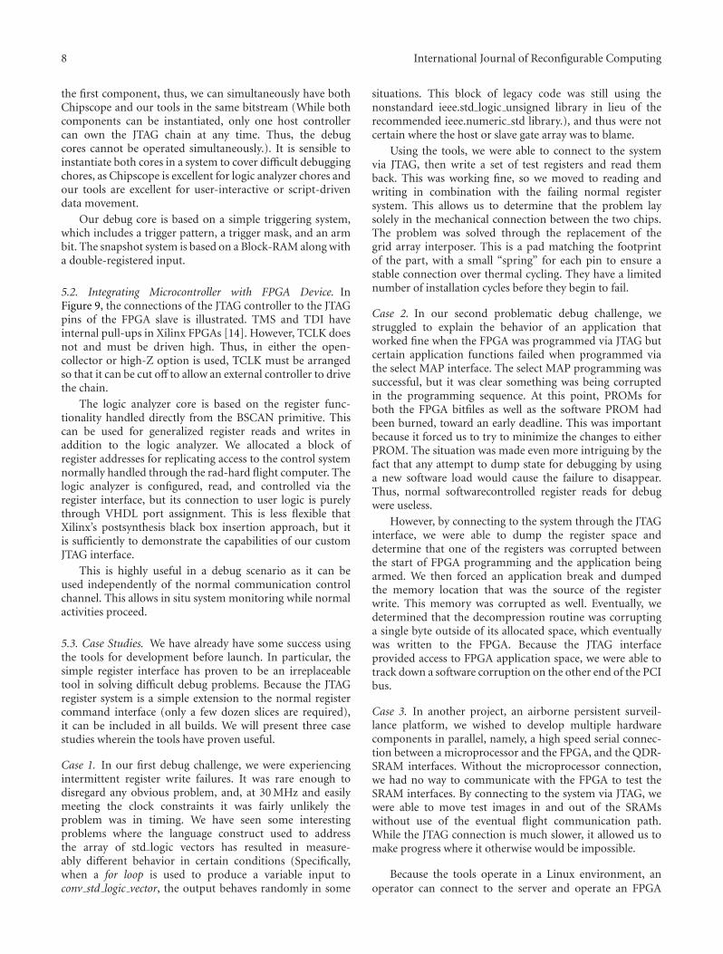
5.2. Integrating Microcontroller with FPGA Device. InFigure 9, the connections of the JTAG controller to the JTAGpins of the FPGA slave is illustrated. TMS and TDI haveinternal pull-ups in Xilinx FPGAs [14]. However, TCLK doesnot and must be driven high. Thus, in either the open-collector or high-Z option is used, TCLK must be arrangedso that it can be cut off to allow an external controller to drivethe chain.
The logic analyzer core is based on the register func-tionality handled directly from the BSCAN primitive. Thiscan be used for generalized register reads and writes inaddition to the logic analyzer. We allocated a block ofregister addresses for replicating access to the control systemnormally handled through the rad-hard flight computer. Thelogic analyzer is configured, read, and controlled via theregister interface, but its connection to user logic is purelythrough VHDL port assignment. This is less flexible thatXilinx’s postsynthesis black box insertion approach, but itis sufficiently to demonstrate the capabilities of our customJTAG interface.
This is highly useful in a debug scenario as it can beused independently of the normal communication controlchannel. This allows in situ system monitoring while normalactivities proceed.
5.3. Case Studies. We have already have some success usingthe tools for development before launch. In particular, thesimple register interface has proven to be an irreplaceabletool in solving difficult debug problems. Because the JTAGregister system is a simple extension to the normal registercommand interface (only a few dozen slices are required),it can be included in all builds. We will present three casestudies wherein the tools have proven useful.
Case 1. In our first debug challenge, we were experiencingintermittent register write failures. It was rare enough todisregard any obvious problem, and, at 30 MHz and easilymeeting the clock constraints it was fairly unlikely theproblem was in timing. We have seen some interestingproblems where the language construct used to addressthe array of std logic vectors has resulted in measure-ably different behavior in certain conditions (Specifically,when a for loop is used to produce a variable input toconv std logic vector, the output behaves randomly in some
situations. This block of legacy code was still using thenonstandard ieee.std logic unsigned library in lieu of therecommended ieee.numeric std library.), and thus were notcertain where the host or slave gate array was to blame.
Using the tools, we were able to connect to the systemvia JTAG, then write a set of test registers and read themback. This was working fine, so we moved to reading andwriting in combination with the failing normal registersystem. This allows us to determine that the problem laysolely in the mechanical connection between the two chips.The problem was solved through the replacement of thegrid array interposer. This is a pad matching the footprintof the part, with a small “spring” for each pin to ensure astable connection over thermal cycling. They have a limitednumber of installation cycles before they begin to fail.
Case 2. In our second problematic debug challenge, westruggled to explain the behavior of an application thatworked fine when the FPGA was programmed via JTAG butcertain application functions failed when programmed viathe select MAP interface. The select MAP programming wassuccessful, but it was clear something was being corruptedin the programming sequence. At this point, PROMs forboth the FPGA bitfiles as well as the software PROM hadbeen burned, toward an early deadline. This was importantbecause it forced us to try to minimize the changes to eitherPROM. The situation was made even more intriguing by thefact that any attempt to dump state for debugging by usinga new software load would cause the failure to disappear.Thus, normal softwarecontrolled register reads for debugwere useless.
However, by connecting to the system through the JTAGinterface, we were able to dump the register space anddetermine that one of the registers was corrupted betweenthe start of FPGA programming and the application beingarmed. We then forced an application break and dumpedthe memory location that was the source of the registerwrite. This memory was corrupted as well. Eventually, wedetermined that the decompression routine was corruptinga single byte outside of its allocated space, which eventuallywas written to the FPGA. Because the JTAG interfaceprovided access to FPGA application space, we were able totrack down a software corruption on the other end of the PCIbus.
Case 3. In another project, an airborne persistent surveil-lance platform, we wished to develop multiple hardwarecomponents in parallel, namely, a high speed serial connec-tion between a microprocessor and the FPGA, and the QDR-SRAM interfaces. Without the microprocessor connection,we had no way to communicate with the FPGA to test theSRAM interfaces. By connecting to the system via JTAG, wewere able to move test images in and out of the SRAMswithout use of the eventual flight communication path.While the JTAG connection is much slower, it allowed us tomake progress where it otherwise would be impossible.
Because the tools operate in a Linux environment, anoperator can connect to the server and operate an FPGA
International Journal of Reconfigurable Computing 9
Figure 10: T-SDR modules loaded in a compact-PCI test chassis.The use of commodity compact-PCI chassis allow for cheap andefficient development cycles. Shown right to left are RTSP, DCR,and SVIM in COTS cPCI test chassis.
board remotely from the command line, without having adirect board interface. This is useful not just in a laboratoryor commercial setting, but also in educational settings wherecommunicating with a development board is nontrivial.For instance, common Spartan 3 boards for universityclasses often have no way to talk to the FPGA exceptbuttons and LED readouts. These tools can allow sufficientlyfast communication to open a wide variety of applicationdevelopment opportunities.
The functional prototype system operates through a USBconnection. This makes it very similiar to a commercial JTAGcable. However, our initial system is just a demonstrationfor the final system, which will be implemented in a rad-hard microcontroller and connected via SpaceWire to thesatellite ground interface. At that point, the interface to theJTAG controller will be via SpaceWire packets, which willbe translated from the satellite’s real-time command andtelemetry interface.
6. Results and Performance Testing
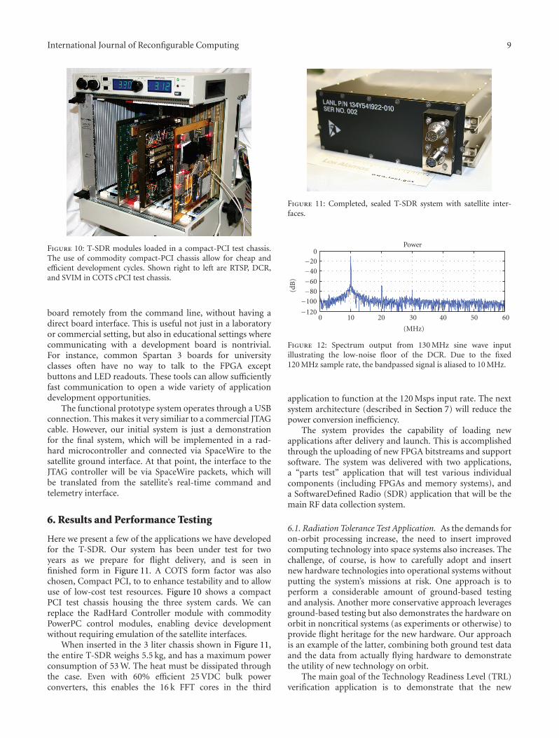
Here we present a few of the applications we have developedfor the T-SDR. Our system has been under test for twoyears as we prepare for flight delivery, and is seen infinished form in Figure 11. A COTS form factor was alsochosen, Compact PCI, to to enhance testability and to allowuse of low-cost test resources. Figure 10 shows a compactPCI test chassis housing the three system cards. We canreplace the RadHard Controller module with commodityPowerPC control modules, enabling device developmentwithout requiring emulation of the satellite interfaces.
When inserted in the 3 liter chassis shown in Figure 11,the entire T-SDR weighs 5.5 kg, and has a maximum powerconsumption of 53 W. The heat must be dissipated throughthe case. Even with 60% efficient 25 VDC bulk powerconverters, this enables the 16 k FFT cores in the third
Figure 11: Completed, sealed T-SDR system with satellite inter-faces.
Power
−120
−100
−80
−60
−40−20
0
(dB
)
0 10 20 30 40 50 60
(MHz)
Figure 12: Spectrum output from 130 MHz sine wave inputillustrating the low-noise floor of the DCR. Due to the fixed120 MHz sample rate, the bandpassed signal is aliased to 10 MHz.
application to function at the 120 Msps input rate. The nextsystem architecture (described in Section 7) will reduce thepower conversion inefficiency.
The system provides the capability of loading newapplications after delivery and launch. This is accomplishedthrough the uploading of new FPGA bitstreams and supportsoftware. The system was delivered with two applications,a “parts test” application that will test various individualcomponents (including FPGAs and memory systems), anda SoftwareDefined Radio (SDR) application that will be themain RF data collection system.
6.1. Radiation Tolerance Test Application. As the demands foron-orbit processing increase, the need to insert improvedcomputing technology into space systems also increases. Thechallenge, of course, is how to carefully adopt and insertnew hardware technologies into operational systems withoutputting the system’s missions at risk. One approach is toperform a considerable amount of ground-based testingand analysis. Another more conservative approach leveragesground-based testing but also demonstrates the hardware onorbit in noncritical systems (as experiments or otherwise) toprovide flight heritage for the new hardware. Our approachis an example of the latter, combining both ground test dataand the data from actually flying hardware to demonstratethe utility of new technology on orbit.
The main goal of the Technology Readiness Level (TRL)verification application is to demonstrate that the new
10 International Journal of Reconfigurable Computing
120 MS 16 bitADC
1/3 overlap delay
Programmablewindow
16 k pt FFT
16 k pt FFT
Real
ImagPhase translation
CORDIC
Mag
Phase
logcompression Run-length
encoding
Compresseddata stream
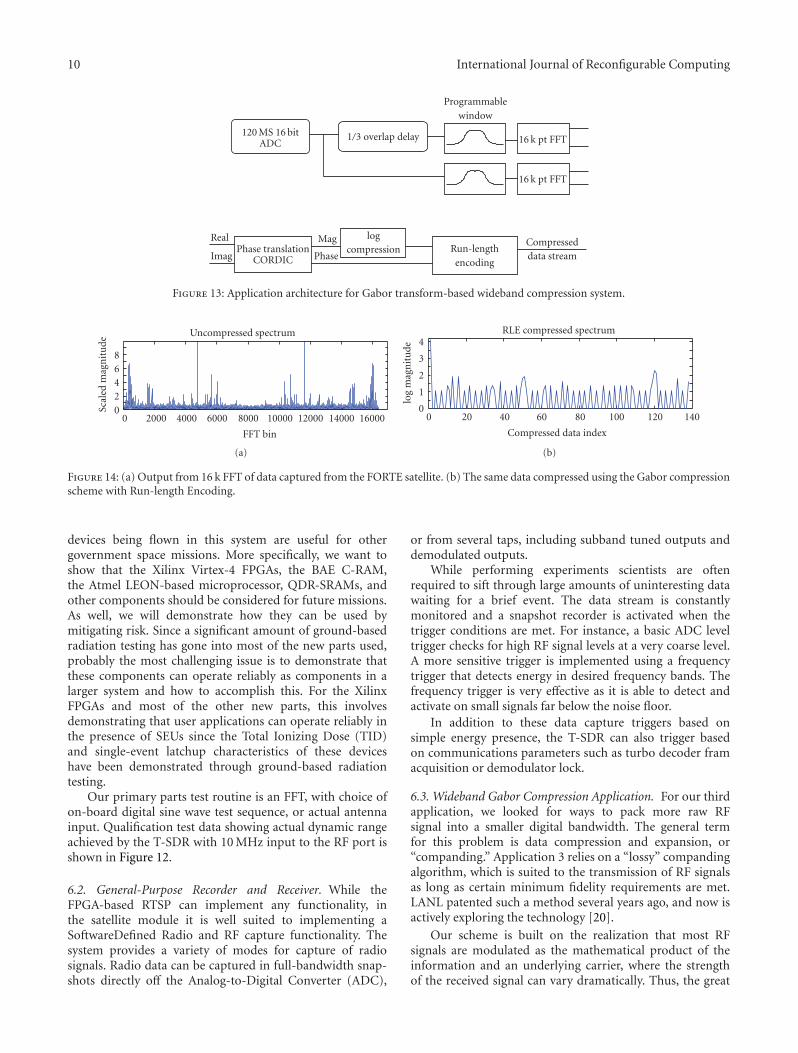
Figure 13: Application architecture for Gabor transform-based wideband compression system.
Uncompressed spectrum
02468
Scal
edm
agn
itu
de
0 2000 4000 6000 8000 10000 12000 14000 16000
FFT bin
(a)
RLE compressed spectrum
0
1
2
3
4
log
mag
nit
ude
0 20 40 60 80 100 120 140
Compressed data index
(b)
Figure 14: (a) Output from 16 k FFT of data captured from the FORTE satellite. (b) The same data compressed using the Gabor compressionscheme with Run-length Encoding.
devices being flown in this system are useful for othergovernment space missions. More specifically, we want toshow that the Xilinx Virtex-4 FPGAs, the BAE C-RAM,the Atmel LEON-based microprocessor, QDR-SRAMs, andother components should be considered for future missions.As well, we will demonstrate how they can be used bymitigating risk. Since a significant amount of ground-basedradiation testing has gone into most of the new parts used,probably the most challenging issue is to demonstrate thatthese components can operate reliably as components in alarger system and how to accomplish this. For the XilinxFPGAs and most of the other new parts, this involvesdemonstrating that user applications can operate reliably inthe presence of SEUs since the Total Ionizing Dose (TID)and single-event latchup characteristics of these deviceshave been demonstrated through ground-based radiationtesting.
Our primary parts test routine is an FFT, with choice ofon-board digital sine wave test sequence, or actual antennainput. Qualification test data showing actual dynamic rangeachieved by the T-SDR with 10 MHz input to the RF port isshown in Figure 12.
6.2. General-Purpose Recorder and Receiver. While theFPGA-based RTSP can implement any functionality, inthe satellite module it is well suited to implementing aSoftwareDefined Radio and RF capture functionality. Thesystem provides a variety of modes for capture of radiosignals. Radio data can be captured in full-bandwidth snap-shots directly off the Analog-to-Digital Converter (ADC),
or from several taps, including subband tuned outputs anddemodulated outputs.
While performing experiments scientists are oftenrequired to sift through large amounts of uninteresting datawaiting for a brief event. The data stream is constantlymonitored and a snapshot recorder is activated when thetrigger conditions are met. For instance, a basic ADC leveltrigger checks for high RF signal levels at a very coarse level.A more sensitive trigger is implemented using a frequencytrigger that detects energy in desired frequency bands. Thefrequency trigger is very effective as it is able to detect andactivate on small signals far below the noise floor.
In addition to these data capture triggers based onsimple energy presence, the T-SDR can also trigger basedon communications parameters such as turbo decoder framacquisition or demodulator lock.
6.3. Wideband Gabor Compression Application. For our thirdapplication, we looked for ways to pack more raw RFsignal into a smaller digital bandwidth. The general termfor this problem is data compression and expansion, or“companding.” Application 3 relies on a “lossy” compandingalgorithm, which is suited to the transmission of RF signalsas long as certain minimum fidelity requirements are met.LANL patented such a method several years ago, and now isactively exploring the technology [20].
Our scheme is built on the realization that most RFsignals are modulated as the mathematical product of theinformation and an underlying carrier, where the strengthof the received signal can vary dramatically. Thus, the great
International Journal of Reconfigurable Computing 11
RF AMP
RF AMP
RF AMP
Tuner/ADC
Virtex-5
...
Tuner/ADC
Virtex-5
Tuner/ADC
Virtex-5
Sub-band tuners& compressors
uT
CA
500
Gbs
mu
lti-
seri
albu
s
Beamformers
Virtex-5
4× 256Mbytes
Virtex-5
4× 256Mbytes
Out
Figure 15: Multiple-Input Multiple-Output (MIMO) architecture for Virtex-5 FPGA-based beamformer.
majority of practical sensor applications are multiplicativemodulation processes, which only require constant relativeprecision. This implies that logarithmic magnitude represen-tations may be used without loss of resolution, as long as theyare properly scaled. Few assumptions can be made aboutphase, requiring more information to be kept. The basicblock diagram of Application 3 is illustrated in Figure 13.
Given the above assumptions, our process consists ofapplying a logarithmic transform to the output of a Fouriertransform. The purpose of the frequency transform is toconvert convolution processes to multiplication in frequencyspace, and to separate various signals that overlap in the timeseries, but which are separate in the frequency space. Use ofthe log transform then allows the multiplicative signals stillcontained in each frequency sample to be treated as additivesuperpositions.
The 120 Mega-Sample/second input data is subjectedto a 1/3 overlap delay (1/3 of the FFT size of 16 k samples)to produce two data streams. This allows the output tocompletely cover the input signal after the windowingfunction is applied. Without the overlap delay, signalsoccurring at the edge of the transform might be maskedand inadvertently destroyed. The two signals are then fedthrough a window multiplier to reduce spectral leakageand to allow near-perfect reconstruction. The outputs ofthe windowing operator are suitably delayed such that bothsignals can be presented to the FFT simultaneously. This isnecessary because the system uses a single FFT to computethe transform of both streams, reducing the area and powerrequirements for the large 16 k point FFT. Because the inputsto the FFT are real, the output of the FFT is separable intotwo unique frequency transforms.
The output of the FFT is then fed into a rectangular/polarCORDIC transform. This is a pipelined core that convertsthe complex FFT output into corresponding polar repre-sentation consisting of magnitude and phase, which is thenatural domain to either compress or to interpret man-madesignals. At this point the magnitude enters a lookup table,providing Mu Law scaling, which is linear at low amplitudesand logarithmic at larger amplitudes, providing a balance
between range and precision. At present we do not processthe phase, but methods of removing phase trend informationand compressing it are very promising, and under study.
Finally the data enters a run length coder, with variablethreshold, so that only magnitude values over a chosen levelare accepted. For the discarded values below threshold, thecoder discards both magnitude and phase, and substitutesa sequence length code instead. In this way, larger orsmaller data compaction ratios are achieved, dependingon the degree of fidelity required. Figure 14 illustrates theeffectiveness of the scheme with data collected on FORTE,another LANL satellite. A sample size of 16 k real pointsis reduced to 140 points in log-polar representation (withmagnitude and phase). In this scheme, low energy frequencybins are discarded and the length of runs of discarded binsare recorded.
7. Summary and Work in Progress
Even as the receiver was developed, new COTS hardwareappeared that dramatically changed architectural possibili-ties again. The two most significant developments for LANLwere the following.
(i) The advent of Multi-Gigabit Serial cores in FPGAs,DSPs, and microprocessors. These hard IP blocksenable all-serial modular systems.
(ii) The development of silicon-on-insulator ADC suchas the TI5424, which offer very strong Rad Toler-ance while providing input bandwidths exceedinga GHz and sample rates > 400 Msps. This enablescontinuous band coverage from Direct Conversionarchitectures.
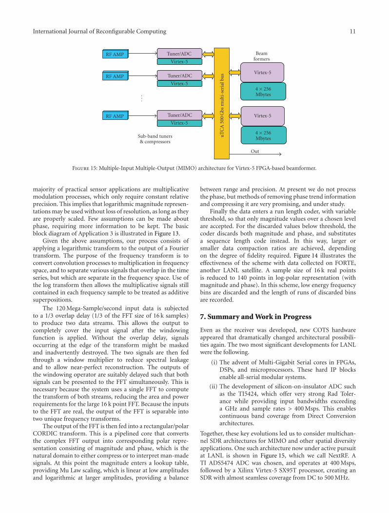
Together, these key evolutions led us to consider multichan-nel SDR architectures for MIMO and other spatial diversityapplications. One such architecture now under active pursuitat LANL is shown in Figure 15, which we call NextRF. ATI ADS5474 ADC was chosen, and operates at 400 Msps,followed by a Xilinx Virtex-5 SX95T processor, creating anSDR with almost seamless coverage from DC to 500 MHz.
12 International Journal of Reconfigurable Computing
Test results are expected from NextRF by 2010. Oursimulations indicate that the V5SX95 with the 16 k FFT andCORDIC cores described above can operate at 400 MHz, andoccupancy is about 18% of the device. In this partitioningscheme, the compressor runs within the receiver head, anddelivers a serial stream of digital data to postprocessors whichcombine and further reduce the signal size into a final outputdatastream.
Acknowledgments
The LANL team gratefully acknowledges long-term supportfrom DOE NA-22, DARPA, and other DOD agencies indevelopment of all our SDR work. Only through suchlong-term support can a new capability be fully developed.The authors also recognize the contributions of our com-mercial partners, Xilinx, Lockheed-Martin, BAE Systems,Linear Technology, and Texas Instruments. This documentis released under LA-UR 10-06455.
References
[1] P. S. Graham, M. Caffrey, M. J. Wirthlin, and D. E. J.N. H. Rollins, “Reconfigurable computing in space: fromcurrent technology to reconfigurable systems-on-a-chip,” inProceedings of the IEEE Aerospace Conference, pp. 2399–2410,2003.
[2] Published specifications of the BAE Rad750 PPC (50Mips/Watt) device, or the Atmel AT697E (100Mips/Watt,versus measured Virtex-4 performance (50 GOps/Watt) atseveral facilities).
[3] H. Quinn and P. Graham, “Terrestrial-based radiation upsets:a cautionary tale,” in Proceedings of the 13th Annual IEEE Sym-posium on Field-Programmable Custom Computing Machines(FCCM ’05), pp. 193–202, April 2005.
[4] H. Quinn, P. Graham, and B. Pratt, “An automated approachto estimating hardness assurance issues in triple-modularredundancy circuits in xilinx FPGAs,” IEEE Transactions onNuclear Science, vol. 55, no. 6, pp. 3070–3076, 2008.
[5] H. Quinn, P. Graham, J. Krone, M. Caffrey, and S. Rezgui,“Radiation-induced multi-bit upsets in SRAM-based FPGAs,”IEEE Transactions on Nuclear Science, vol. 52, no. 6, pp. 2455–2461, 2005.
[6] R. Crochiere and C. Rabiner, Multi-Rate Digital Signal Process-ing, Prentice-Hall, Upper Saddle River, NJ, USA, 1983.
[7] CCIR Reports 341-6, 258-5, & 670-1, International Telecom-munication Union, Geneva, Switzerland.
[8] S. Dhawana, O. Bakera, R. Khannad, et al., “Radiation resistantdc-dc power conversion with voltage ratios > 10 capable ofoperating in high magnetic field for lhc upgrade detectors,” inProceedings of the Topical Workshop on Electronics for ParticlePhysics, 2008.
[9] E. Johnson, M. Caffrey, P. Graham, N. Rollins, and M.Wirthlin, “Accelerator validation of an FPGA SEU simulator,”IEEE Transactions on Nuclear Science, vol. 50, no. 6, pp. 2147–2157, 2003.
[10] P. S. Ostler, M. P. Caffrey, D. S. Gibelyou,, et al., “SRAM FPGAreliability analysis for harsh radiation environments,” IEEETransactions on Nuclear Science, vol. 56, no. 6, pp. 3519–3526,2009.
[11] K. Morgan, M. Caffrey, P. Graham, E. Johnson, B. Pratt, andM. Wirthlin, “SEU-induced persistent error propagation inFPGAs,” IEEE Transactions on Nuclear Science, vol. 52, no. 6,pp. 2438–2445, 2005.
[12] “Open On-Chip Debugger: Free and Open On-Chip Debug-ging, In-System Programming and Boundary-Scan Testing,”2008, http://openocd.berlios.de/web/.
[13] “URJTAG: Universal JTAG library, server and tools,” 2008,http://www.urjtag.org/book/index.html.
[14] “Xilinx UG071 Virtex-4 Configuration Guide,” 2006, http://www.xilinx.com/support/documentation/user guides/ug070.pdf.
[15] “PicoBlaze User Resources,” 2008, http://www.xilinx.com/ipcenter/processor central/picoblaze/picoblaze user resources.htm.
[16] “PIC18F2455/2550/4455/4550 Product Family,” 2007, http://www.microchip.com/wwwproducts/Devices.aspx?dDocName=dDocName=en010280.
[17] “Xilinx In-System Programming Using an EmbeddedMicrocontroller,” 2007, http://www.xilinx.com/support/documentation/application notes/xapp058.pdf.
[18] “Using the JTAG Interface as a General-PurposeCommunication Port,” 2005, http://www.xilinx.com/support/support/documentation/user guides/ug070.pdf.
[19] “Xilinx Chipscope Pro Tool,” 2009, http://www.xilinx.com/ise/optionalprod/cspro.htm.
[20] M. Dunham, “Logarithmic compression methods for spectraldata,” US Patent no. 6,529,927, 2003.

International Journal of
AerospaceEngineeringHindawi Publishing Corporationhttp://www.hindawi.com Volume 2010
RoboticsJournal of
Hindawi Publishing Corporationhttp://www.hindawi.com Volume 2014
Hindawi Publishing Corporationhttp://www.hindawi.com Volume 2014
Active and Passive Electronic Components
Control Scienceand Engineering
Journal of
Hindawi Publishing Corporationhttp://www.hindawi.com Volume 2014
International Journal of
RotatingMachinery
Hindawi Publishing Corporationhttp://www.hindawi.com Volume 2014
Hindawi Publishing Corporation http://www.hindawi.com
Journal ofEngineeringVolume 2014
Submit your manuscripts athttp://www.hindawi.com
VLSI Design
Hindawi Publishing Corporationhttp://www.hindawi.com Volume 2014
Hindawi Publishing Corporationhttp://www.hindawi.com Volume 2014
Shock and Vibration
Hindawi Publishing Corporationhttp://www.hindawi.com Volume 2014
Civil EngineeringAdvances in
Acoustics and VibrationAdvances in
Hindawi Publishing Corporationhttp://www.hindawi.com Volume 2014
Hindawi Publishing Corporationhttp://www.hindawi.com Volume 2014
Electrical and Computer Engineering
Journal of
Advances inOptoElectronics
Hindawi Publishing Corporation http://www.hindawi.com
Volume 2014
The Scientific World JournalHindawi Publishing Corporation http://www.hindawi.com Volume 2014
SensorsJournal of
Hindawi Publishing Corporationhttp://www.hindawi.com Volume 2014
Modelling & Simulation in EngineeringHindawi Publishing Corporation http://www.hindawi.com Volume 2014
Hindawi Publishing Corporationhttp://www.hindawi.com Volume 2014
Chemical EngineeringInternational Journal of Antennas and
Propagation
International Journal of
Hindawi Publishing Corporationhttp://www.hindawi.com Volume 2014
Hindawi Publishing Corporationhttp://www.hindawi.com Volume 2014
Navigation and Observation
International Journal of
Hindawi Publishing Corporationhttp://www.hindawi.com Volume 2014
DistributedSensor Networks
International Journal of