Embed Size (px)
Citation preview
SPACE-FLIGHT DESIGN VERIFICATION TECHNIQUES
By Omar HaddadReSpace/MAPLD Conference
August 2011
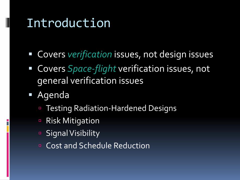
Introduction
Covers verification issues, not design issues
Covers Space-flight verification issues, not general verification issues
Agenda
Testing Radiation-Hardened Designs
Risk Mitigation
Signal Visibility
Cost and Schedule Reduction
A discussion of the unique challenges of verifying designs destined for space environments
Testing Radiation-Hardened Designs
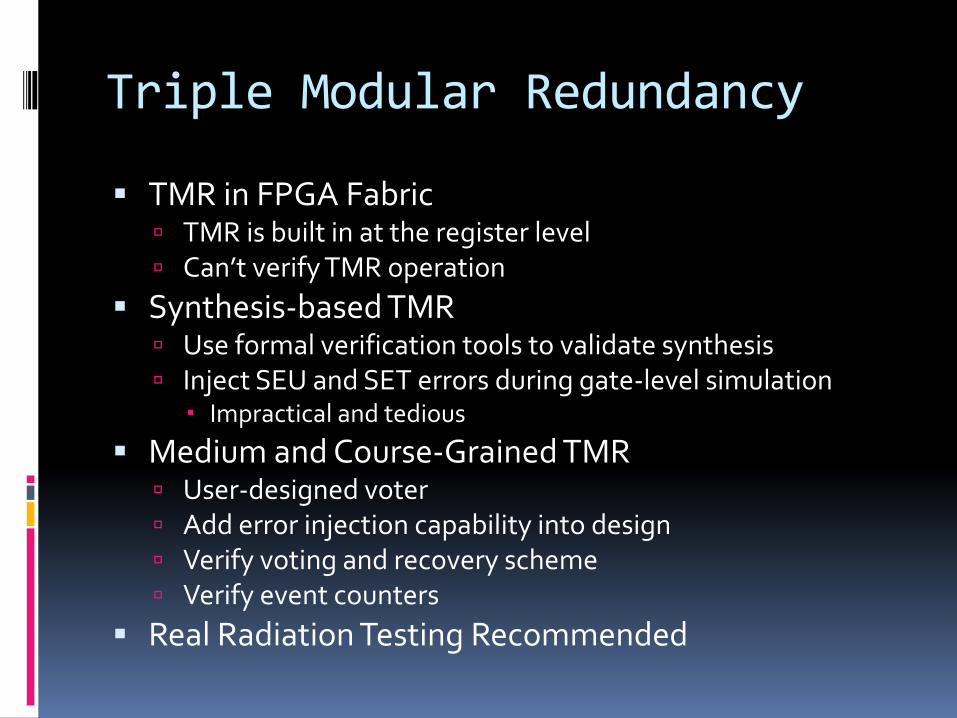
Triple Modular Redundancy
TMR in FPGA Fabric TMR is built in at the register level Can’t verify TMR operation
Synthesis-based TMR Use formal verification tools to validate synthesis Inject SEU and SET errors during gate-level simulation Impractical and tedious
Medium and Course-Grained TMR User-designed voter Add error injection capability into design Verify voting and recovery scheme Verify event counters
Real Radiation Testing Recommended
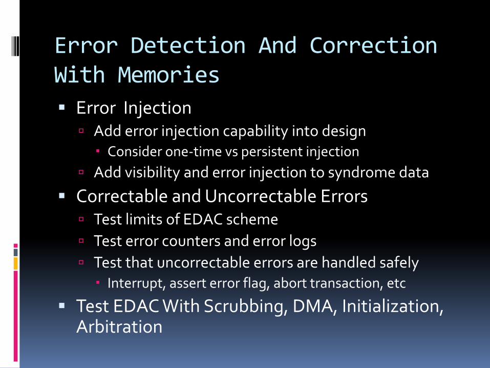
Error Detection And Correction With Memories
Error Injection Add error injection capability into design Consider one-time vs persistent injection
Add visibility and error injection to syndrome data
Correctable and Uncorrectable Errors Test limits of EDAC scheme
Test error counters and error logs
Test that uncorrectable errors are handled safely Interrupt, assert error flag, abort transaction, etc
Test EDAC With Scrubbing, DMA, Initialization, Arbitration
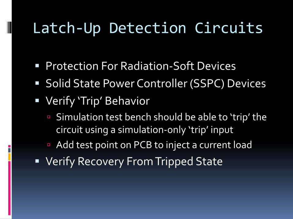
Latch-Up Detection Circuits
Protection For Radiation-Soft Devices
Solid State Power Controller (SSPC) Devices
Verify ‘Trip’ Behavior
Simulation test bench should be able to ‘trip’ the circuit using a simulation-only ‘trip’ input
Add test point on PCB to inject a current load
Verify Recovery From Tripped State
Adding Visibility For Automated Simulations
Some transactions are not ‘visible’ to automated tests Memory scrubbing, mode register writes, SDRAM
refresh cycles
Modify simulation models to detect such transactions SDRAM simulation models
Use non-synthesized RTL code to detect such transactions -translate on/off directives
Finite State Machine Operation
Radiation Environment SEU and SET could cause invalid transitions to,
possibly, invalid states
Fault Detection Verify that fault conditions are detected
Use translate on/off directives to inject faults or ‘disable’ the FSM
Verify Recovery Scheme FSM reset, normal operation
Use FSM coverage tools
Watchdogs
Commonly used to detect faults
Implement test-mode in simulation environment
Advances watchdog time quicker
Reduce simulation time
Use different VHDL package file for simulation
Defines terminal counts, time parameters, etc
Verify recovery from watchdog timeout state
Exercise entire range of timer values
When “failure is not an option”, risk must be managed and mitigated as much as possible using good verification techniques
Risk Mitigation
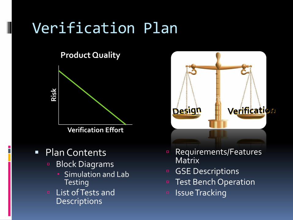
Verification Plan
Ris
k
Verification Effort
Product Quality
Plan Contents Block Diagrams Simulation and Lab
Testing
List of Tests and Descriptions
Requirements/Features Matrix
GSE Descriptions Test Bench Operation Issue Tracking
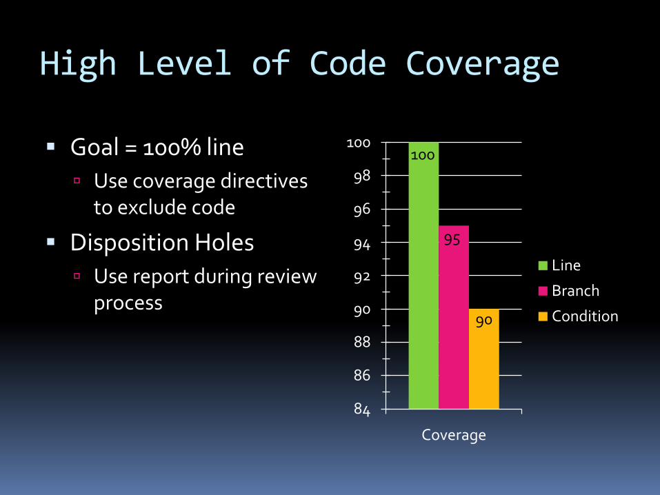
High Level of Code Coverage
Goal = 100% line
Use coverage directives to exclude code
Disposition Holes
Use report during review process
100
95
90
84
86
88
90
92
94
96
98
100
Coverage
Line
Branch
Condition
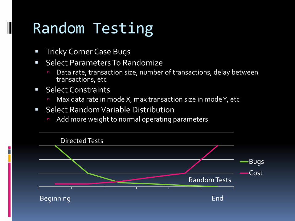
Random Testing
Tricky Corner Case Bugs
Select Parameters To Randomize Data rate, transaction size, number of transactions, delay between
transactions, etc
Select Constraints Max data rate in mode X, max transaction size in mode Y, etc
Select Random Variable Distribution Add more weight to normal operating parameters
Directed Tests
Random Tests
Beginning End
Bugs
Cost
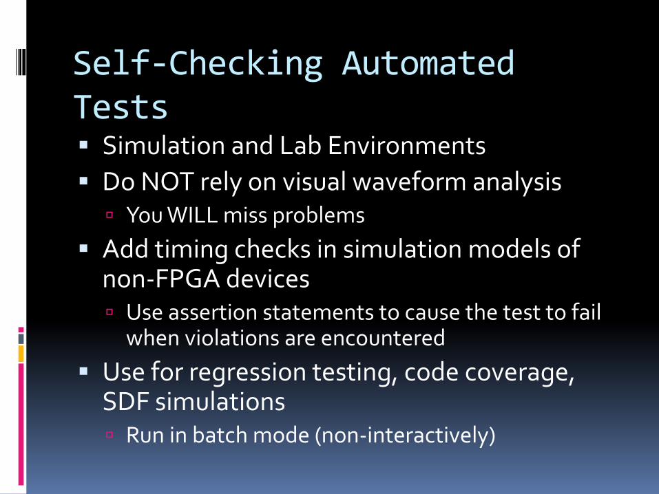
Self-Checking Automated Tests Simulation and Lab Environments
Do NOT rely on visual waveform analysis You WILL miss problems
Add timing checks in simulation models of non-FPGA devices Use assertion statements to cause the test to fail
when violations are encountered
Use for regression testing, code coverage, SDF simulations Run in batch mode (non-interactively)
Requirements Traceability
Create list of design requirements
Create list of design features
Each requirement/feature should be traced back to a verification test
Review that tests adequately exercise requirements/features
Environmental Testing
Automate and Archive
Vary Board Voltages During Thermal Vacuum Testing
Emulates TID exposure effects
Setup/Hold Timing
FPGA Core Voltage
Voltage Regulator Feedback Resistor
Signal Visibility
How to overcome the challenges of signal visibility during environmental testing
Probing Internal FPGA Signals
Actel-Microsemi Silicon Explorer
Can view up to 4 signals simultaneously
FPGA output limited to ~80MHz
Choose JTAG signal buffering and termination wisely
Use differential drivers for higher frequencies
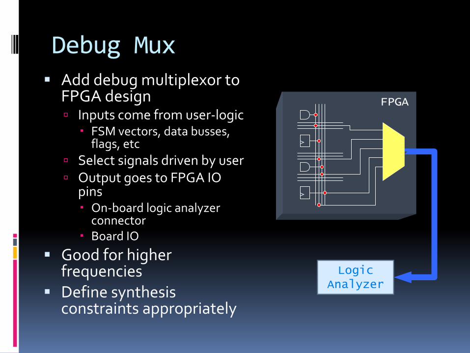
Debug Mux Add debug multiplexor to
FPGA design Inputs come from user-logic FSM vectors, data busses,
flags, etc
Select signals driven by user Output goes to FPGA IO
pins On-board logic analyzer
connector Board IO
Good for higher frequencies
Define synthesis constraints appropriately
FPGA
Logic Analyzer
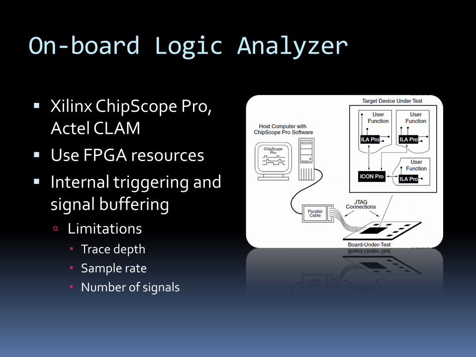
On-board Logic Analyzer
Xilinx ChipScope Pro, Actel CLAM
Use FPGA resources
Internal triggering and signal buffering
Limitations Trace depth
Sample rate
Number of signals
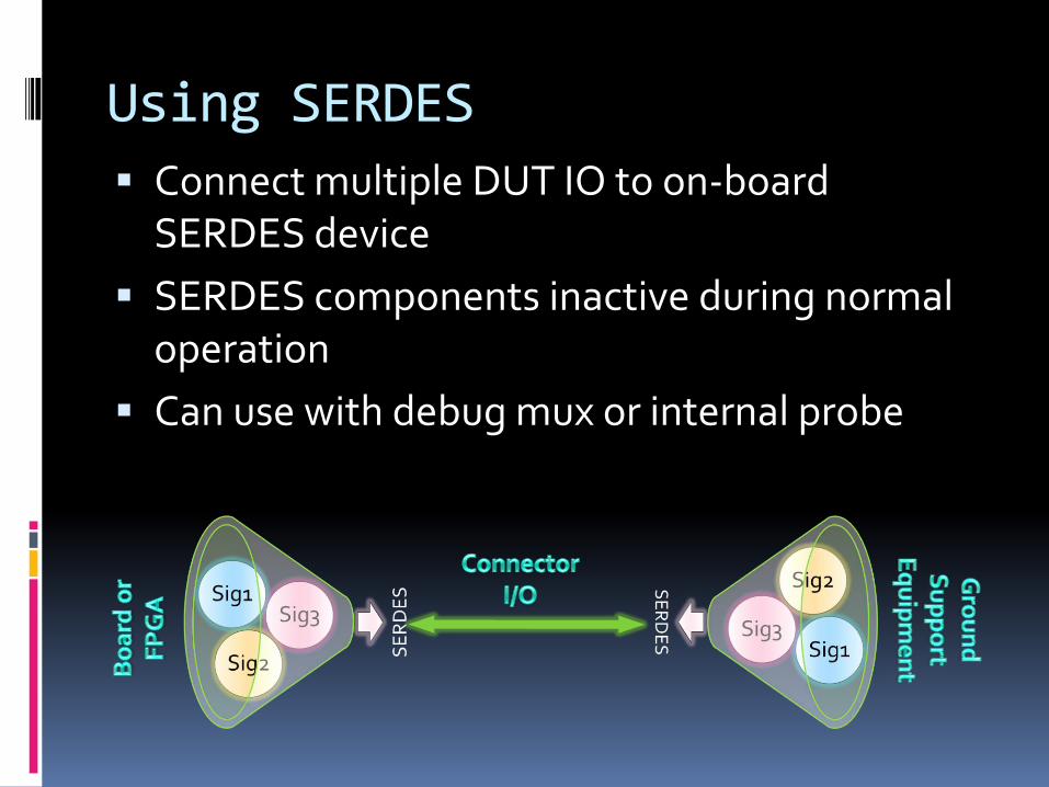
Using SERDES
Connect multiple DUT IO to on-board SERDES device
SERDES components inactive during normal operation
Can use with debug mux or internal probe
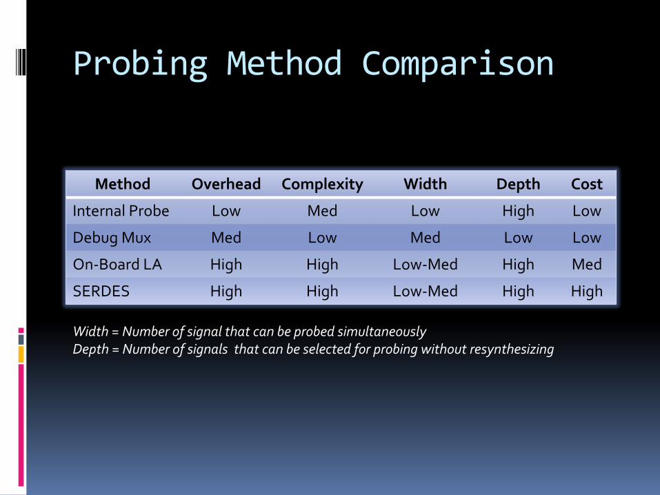
Probing Method Comparison
Method Overhead Complexity Width Depth Cost
Internal Probe Low Med Low High Low
Debug Mux Med Low Med Low Low
On-Board LA High High Low-Med High Med
SERDES High High Low-Med High High
Width = Number of signal that can be probed simultaneouslyDepth = Number of signals that can be selected for probing without resynthesizing
Practical verification tips that help to reduce cost and schedule.
Cost And Schedule Reduction
Simulation Intensive
Invest in developing a high-fidelity simulation environment
Use datasheets to create simulation models
Simulate PCB netlist
Simulate GSE and connectivity to DUT
Use code coverage to ensure that design is fully tested
Avoid costly PCB re-spins
Avoid late-phase bugs
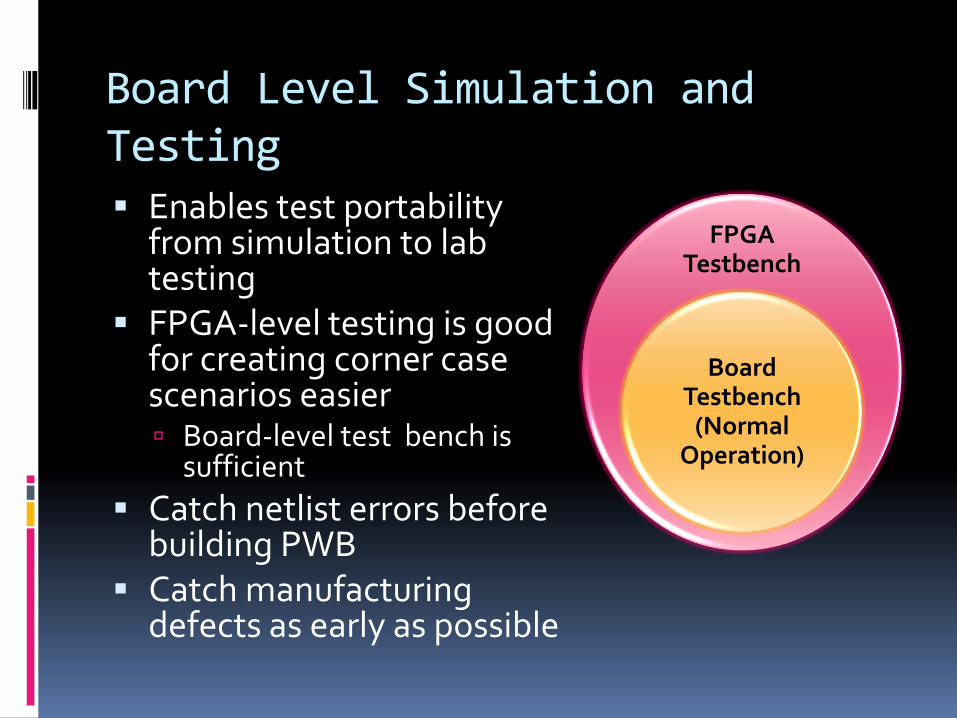
Board Level Simulation and Testing Enables test portability
from simulation to lab testing
FPGA-level testing is good for creating corner case scenarios easier Board-level test bench is
sufficient
Catch netlist errors before building PWB
Catch manufacturing defects as early as possible
FPGA Testbench
Board Testbench
(Normal Operation)
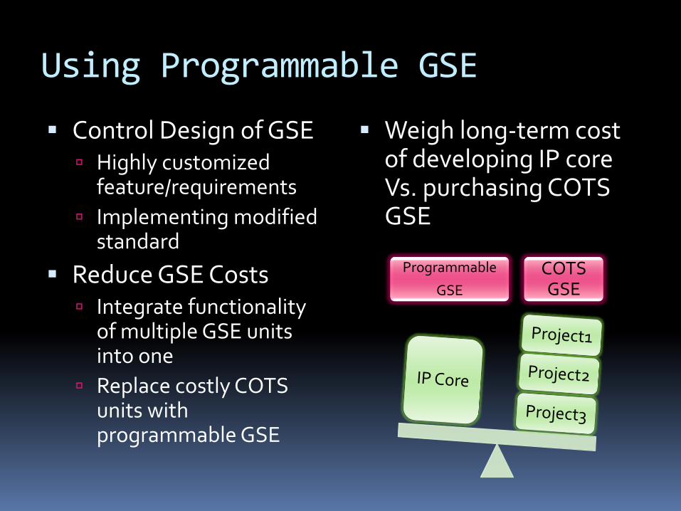
Using Programmable GSE
Control Design of GSE Highly customized
feature/requirements
Implementing modified standard
Reduce GSE Costs Integrate functionality
of multiple GSE units into one
Replace costly COTS units with programmable GSE
Weigh long-term cost of developing IP core Vs. purchasing COTS GSE
Programmable
GSE
COTS GSE
Libraries of Verification IP
Use Standardized Interfaces Easier to mix and match cores needed
Easier to share with others
Interconnect bus
Thorough Documentation Allows others to use IP properly
HW and SW Elements Document, develop, and manage both elements
‘Plug-n-Play’ Hide lower level details as much as possible
Code Re-use
Standardize the IP core design process Use an agency-wide document
Architect designs to maximize reuse Add generic functionality as needed
Avoid temptation to over-design
Use board level test bench Simulation tests can be re-used in lab
Treat board as a black-box Do not force or sample internal signals with tests
Drive and sample board-level IO with GSE simulation models
A GSFC-developed digital design verification process
Case Study: Total Verification System
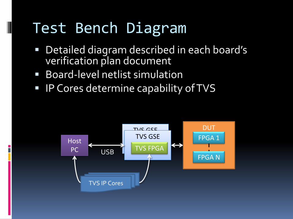
Test Bench Diagram
Detailed diagram described in each board’s verification plan document
Board-level netlist simulation IP Cores determine capability of TVS
TVS GSE
TVS FPGATVS GSE
TVS FPGAHost PC
DUT
FPGA 1
FPGA NUSB
TVS IP Cores
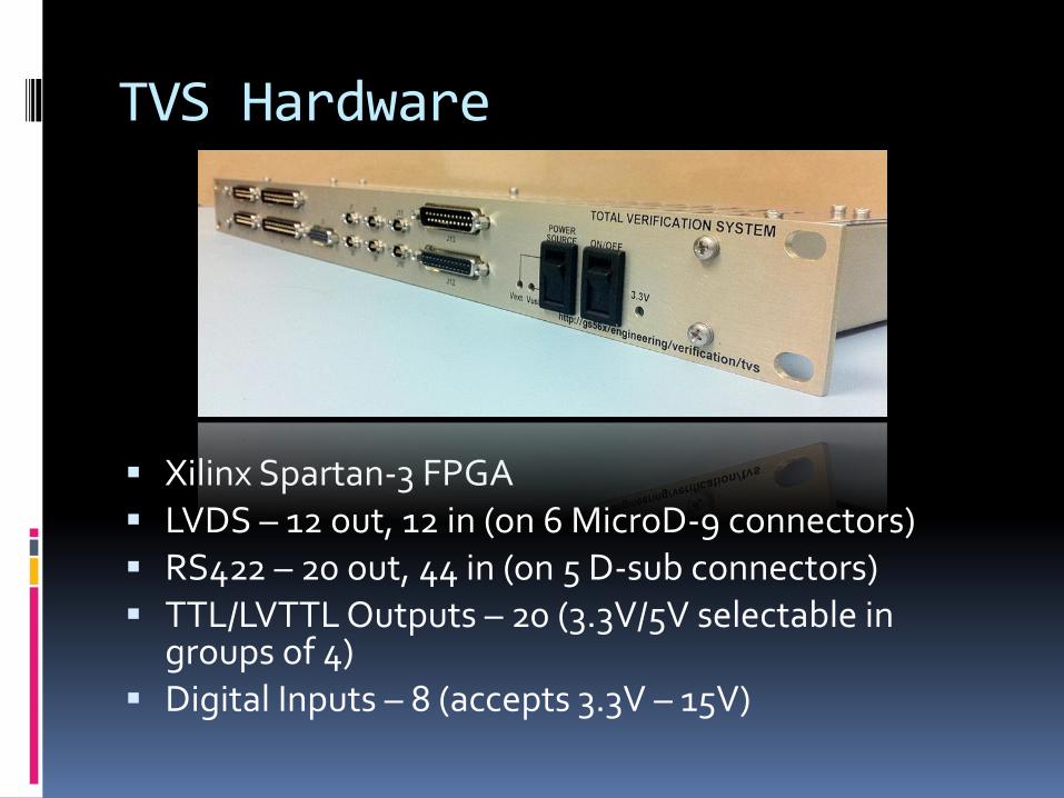
TVS Hardware
Xilinx Spartan-3 FPGA LVDS – 12 out, 12 in (on 6 MicroD-9 connectors) RS422 – 20 out, 44 in (on 5 D-sub connectors) TTL/LVTTL Outputs – 20 (3.3V/5V selectable in
groups of 4) Digital Inputs – 8 (accepts 3.3V – 15V)
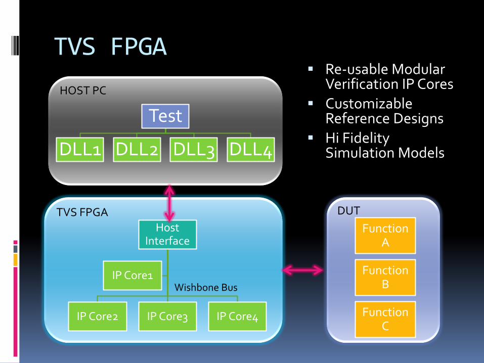
TVS FPGA Re-usable Modular
Verification IP Cores
Customizable Reference Designs
Hi Fidelity Simulation Models
TVS FPGA
Host Interface
IP Core2 IP Core3 IP Core4
IP Core1Wishbone Bus
DUT
Function A
Function B
Function C
HOST PC
Test
DLL1 DLL2 DLL3 DLL4
TVS C++ Classes
Provide high-level functions that hide lower level details
Furnished as DLLs and header files
Can be compiled for use with a variety of programming languages
Used by regression tests to exercise DUT requirements and features
Each IP core is provided with its own DLL
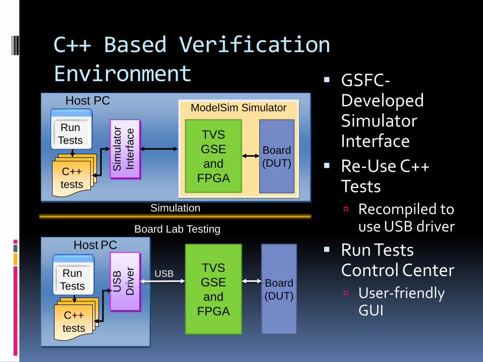
C++ Based Verification Environment GSFC-
Developed Simulator Interface
Re-Use C++ Tests Recompiled to
use USB driver
Run Tests Control Center User-friendly
GUI
Host PCModelSim Simulator
TVS
GSE
and
FPGA
Board
(DUT)Sim
ula
tor
Inte
rface
C++
tests
Host PC
US
B
Drive
r
USB
Simulation
Board Lab Testing
TVS
GSE
and
FPGA
Board
(DUT)
Run
Tests
C++
tests
Run
Tests
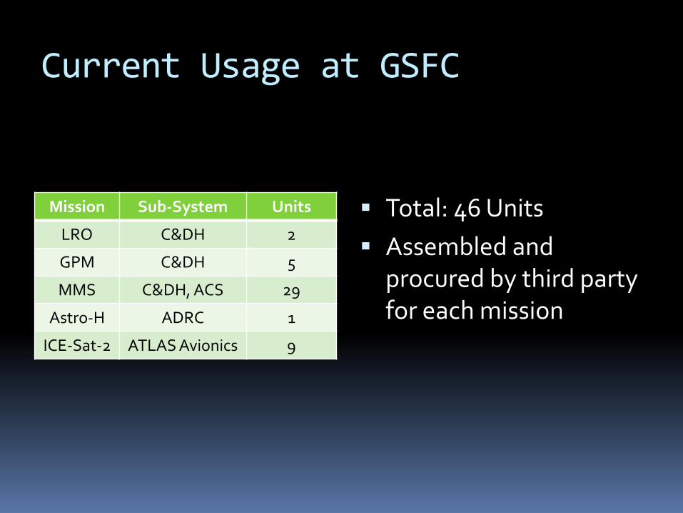
Current Usage at GSFC
Mission Sub-System Units
LRO C&DH 2
GPM C&DH 5
MMS C&DH, ACS 29
Astro-H ADRC 1
ICE-Sat-2 ATLAS Avionics 9
Total: 46 Units
Assembled and procured by third party for each mission
Commercialization Effort
TVS HW and SW available for commercialization
Licensing Agreement for HW
Copyright for SW elements of test bench environment
TVS IP cores can be made available
Copyright for VHDL and C++ code
Contact for more information