Embed Size (px)
Citation preview

ECSS-Q-60-02A 17 July 2007
Space product assurance ASIC and FPGA development
ECSS SecretariatESA-ESTEC
Requirements & Standards DivisionNoordwijk, The Netherlands

2
17 July 2007 ECSS-Q-60-02A
Published by: ESA Requirements and Standards Division ESTEC, P.O. Box 299, 2200 AG Noordwijk, The Netherlands ISSN: 1028-396X Price: € 20 Printed in: The Netherlands Copyright: ©2007 by the European Space Agency for the members of ECSS

3
17 July 2007
ECSS-Q-60-02A
Foreword
This Standard is one of the series of ECSS Standards intended to be applied together for the management, engineering and product assurance in space projects and applications. ECSS is a cooperative effort of the European Space Agency, national space agencies and European industry associations for the purpose of developing and maintaining common standards. Requirements in this Standard are defined in terms of what shall be accomplished, rather than in terms of how to organize and perform the necessary work. This allows existing organizational structures and methods to be applied where they are effective, and for the structures and methods to evolve as necessary without rewriting the standards. The formulation of this Standard takes into account the existing ISO 9000 family of documents. This Standard has been prepared by the ECSS-Q-60-02 Working Group, reviewed by the ECSS Product Assurance Panel and approved by the ECSS Technical Authority.

4
17 July 2007 ECSS-Q-60-02A
(This page is intentionally left blank)

5
17 July 2007
ECSS-Q-60-02A
Contents
Foreword...............................................................................................................................................3
Introduction ..........................................................................................................................................7
1 Scope .......................................................................................................................................9
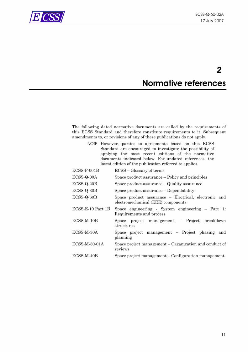
2 Normative references .............................................................................................................11
3 Terms and definitions..............................................................................................................13 3.1 Terms and definitions ................................................................................................................... 13 3.2 Abbreviated terms ....................................................................................................................... 16
4 ASIC and FPGA programme management.............................................................................17 4.1 General........................................................................................................................................ 17 4.2 ASIC and FPGA control plan......................................................................................................... 17 4.3 Management planning tools ....................................................................................................... 18 4.4 Experience summary report ......................................................................................................... 19
5 ASIC and FPGA engineering ...................................................................................................21 5.1 General........................................................................................................................................ 21 5.2 Definition phase ........................................................................................................................... 24 5.3 Architectural design ..................................................................................................................... 28 5.4 Detailed design............................................................................................................................ 30 5.5 Layout .......................................................................................................................................... 33 5.6 Prototype implementation ........................................................................................................... 36 5.7 Design validation and release ..................................................................................................... 36
6 Quality assurance system.......................................................................................................39 6.1 General........................................................................................................................................ 39 6.2 Review meetings.......................................................................................................................... 39 6.3 Risk assessment and risk management........................................................................................ 41
7 Development documentation ................................................................................................43 7.1 General........................................................................................................................................ 43 7.2 Management documentation..................................................................................................... 43 7.3 Design documentation ................................................................................................................ 44 7.4 Application and procurement documents .................................................................................. 47
8 Deliverables............................................................................................................................49 8.1 General........................................................................................................................................ 49 8.2 Deliverable items ......................................................................................................................... 49

6
17 July 2007 ECSS-Q-60-02A
Annex A (normative) Document requirements list and configuration items to be delivered ...............51
Bibliography .......................................................................................................................................53 Figures Figure 1 Development flow (example).......................................................................................... 22 Figure 2 Design documentation ................................................................................................... 45 Tables Table A-1 Deliverables of the ASIC and FPGA development ........................................................... 51

7
17 July 2007
ECSS-Q-60-02A
Introduction
The added responsibilities of developing custom designed devices, as opposed to using off-the-shelf components, make certain management activities crucial to the success of the procurement programme. This was already considered by the applicable standard for “Space product assurance - EEE components”, ECSS-Q-60, that classifies custom designed devices, such as ASIC components, under “Specific components”, for which particular requirements are applicable. The supplier accepts requirements for the development of custom designed components within the boundaries of this standard based on the requirements of the system and its elements, and takes into consideration the operational and environmental requirements of the programme. The supplier implements those requirements into a system which enables to control for instance the technology selection, design, synthesis and simulation, layout and design validation in a schedule compatible with his requirements, and in a cost-efficient way.

8
17 July 2007 ECSS-Q-60-02A
(This page is intentionally left blank)

9
17 July 2007
ECSS-Q-60-02A
1
Scope
This Standard defines a comprehensive set of requirements for the user development of digital, analog and mixed analog-digital custom designed integrated circuits, such as application specific integrated circuits (ASICs) and field programmable gate arrays (FPGAs). The user development includes all activities beginning with setting initial requirements and ending with the validation and release of prototype devices. This Standard is aimed at ensuring that the custom designed components used in space projects meet their requirements in terms of functionality, quality, reliability, schedule and cost. The support of appropriate planning and risk management is essential to ensure that each stage of the development activity is consolidated before starting the subsequent one and to minimize or avoid additional iterations. For the development of standard devices, such as application specific standard products (ASSPs) and IP cores, and devices which implement safety related applications, additional requirements can be included which are not in the scope of this document. The principal sections of this Standard correspond to the main concurrent activities of a circuit development programme. These include: • ASIC and FPGA programme management, • ASIC and FPGA engineering, • ASIC and FPGA quality assurance. The provisions of this document apply to all actors involved in all levels in the realization of space segment hardware and its interfaces. When viewed in a specific project context, the requirements defined in this Standard should be tailored to match the genuine requirements of a particular profile and circumstances of a project.
NOTE Tailoring is a process by which individual requirements or specifications, standards and related documents are evaluated and made applicable to a specific project. This process can result in deletion, addition or modification of requirements.

10
17 July 2007 ECSS-Q-60-02A
(This page is intentionally left blank)
11
17 July 2007
ECSS-Q-60-02A
2
Normative references
The following dated normative documents are called by the requirements of this ECSS Standard and therefore constitute requirements to it. Subsequent amendments to, or revisions of any of these publications do not apply.
NOTE However, parties to agreements based on this ECSS Standard are encouraged to investigate the possibility of applying the most recent editions of the normative documents indicated below. For undated references, the latest edition of the publication referred to applies.
ECSS-P-001B ECSS – Glossary of terms ECSS-Q-00A Space product assurance – Policy and principles ECSS-Q-20B Space product assurance – Quality assurance ECSS-Q-30B Space product assurance – Dependability ECSS-Q-60B Space product assurance – Electrical, electronic and
electromechanical (EEE) components ECSS-E-10 Part 1B Space engineering - System engineering – Part 1:
Requirements and process ECSS-M-10B Space project management – Project breakdown
structures ECSS-M-30A Space project management – Project phasing and
planning ECSS-M-30-01A Space project management – Organization and conduct of
reviews ECSS-M-40B Space project management – Configuration management

12
17 July 2007 ECSS-Q-60-02A
(This page is intentionally left blank)

13
17 July 2007
ECSS-Q-60-02A
3
Terms and definitions
3.1 Terms and definitions For the purposes of this document, the terms and definitions given in ECSS-P-001B and the following apply.
3.1.1 application specific integrated circuit (ASIC) full custom or semi custom designed monolithic integrated circuit that can be digital, analog or a mixed function for one user
3.1.2 ASIC technology totality of all elements required for the design, manufacture and test of ASIC components
Example Design tools and their description, cell libraries, procedures, design rules, process line and test equipment
3.1.3 application specific standard products (ASSP) ASICs designed to make standard products that are made available to a broader range of applications
NOTE ASSPs are most often are provided with a VHDL model and disseminated with documentation
3.1.4 block diagram abstract, graphical presentation of interconnected named boxes (blocks) representing an architectural or functional drawing
3.1.5 cell specific circuit function including digital or analog basic blocks
3.1.6 cell library collection of all mutually compatible cells which conforms to a set of common constraints and standardized interfaces designed and characterized for a specified technology

14
17 July 2007 ECSS-Q-60-02A
3.1.7 data sheet detailed, functional, operational and parametric description of a component
NOTE A data sheet can include, for instance, a block diagram, truth table, pin and signal description, environmental, electrical and performance parameters, tolerances, timing information, and package description.
3.1.8 design flow selection and sequence of engineering methods and tools to be applied during the implementation of the design
3.1.9 design for test (DFT) structure technique used to allow a complex integrated circuit (IC) to be tested
NOTE This can include any mechanism aimed to provide better observability or commandability of internal nodes of the chip not accessible through primary inputs and outputs.
3.1.10 design iteration design changes that occur in any single phase or between two consecutive phases as defined in the ASIC and FPGA development plan, before the design is released for prototype implementation
3.1.11 detail specification procurement specification according to ESCC format that defines, for instance, the maximum ratings, parameter limitations, mechanical outline, pin description and screening requirements
3.1.12 development step major step of the development flow for the ASIC and FPGA development
Example Definition phase, architectural design, detailed design, layout, prototype implementation and design validation
3.1.13 fault coverage measure, expressed as a percentage of the proportion of actually detectable faults versus all possible faults in a digital circuit, for a given set of test patterns and with respect to a specific fault model
3.1.14 field programmable gate array (FPGA) standard semiconductor device that becomes customized when programmed by the user with the FPGA vendor specific software and hardware tools
3.1.15 floorplan abstracted, scaled layout drawing of the die, outlining the form, size and position of the major functional blocks and the pads including power and ground lines, clock distribution and interconnect channels

15
17 July 2007
ECSS-Q-60-02A
3.1.16 HDL model textual model based on a hardware description language (but not a piece of software in itself) suitable for the behavioural or structural description, simulation and by choosing a suitable level of abstraction for automatic netlist generation
3.1.17 intellectual property (IP) core design element that implements a self-standing function or group of functions for which ownership rights exist
Note 1 IP core can be acquired by a customer, for a given price and under an owner-defined license agreement specifying the customer's acquired rights
Note 2 IP core can be supplied as an HDL file (e.g. synthesizable VHDL code or gate-level netlist) and with the essential complementary documentation that allows the customer to successfully integrate and use it in a system (e.g. User's manual and verification files)
3.1.18 macrocell module that contains complex functions in a vendor’s cell library built up out of hard-wired primitive cells
3.1.19 netlist formatted list of cells (basic circuits) and their interconnections
3.1.20 prototype device fabricated ASIC or programmed FPGA used to validate the new design in respect to functionality, performance, operation limits and compatibility with its system
3.1.21 redesign design changes which affect more than two consecutive phases of the ASIC and FPGA development or design changes that are implemented after prototype implementation
3.1.22 stimuli input data set for simulation or test to show a specific functionality or performance of a device
3.1.23 test pattern simulation stimuli and its expected responses (considering specific constraints to meet test equipment requirements) used to show correct behaviour of a device

16
17 July 2007 ECSS-Q-60-02A
3.2 Abbreviated terms For the purposes of this document, the abbreviated terms given in ECSS-P-001B and the following apply. Abbreviation Meaning ACP ASIC and FPGA control plan ADP ASIC and FPGA development plan ARS ASIC and FPGA requirements specification ASCII American standard code for information interchange ASIC application specific integrated circuit ASSP application specific standard product DD design documentation DDR detailed design review DFT design for test DRC design rule check DVP design validation plan EDA electronic design automation EDIF electronic design interchange format ERC electrical rule check ESCC European Space Components Coordination FM flight module part FPGA field-programmable gate array FRA feasibility and risk analysis report GDS graphic design system (industry standard graphics entry tool) HDL hardware description language
NOTE Term used in general for the various “hardware description languages” which are applied for coding during design phase such as VHDL and verilog.
IDMP input data for mask or programming file generation IEEE Institute of Electrical and Electronics Engineers IP intellectual property MoM minutes of meeting P&R place and route JTAG joint test action group LVS layout vs. schematic check NCC netlist comparison check QML qualified manufacturer list RTL register transfer logic SEU single event upset VHDL VHSIC hardware description language

17
17 July 2007
ECSS-Q-60-02A
4
ASIC and FPGA programme management
4.1 General
4.1.1 Introduction The supplier shall establish and implement an ASIC and FPGA development, as part of the component programme (see ECSS-Q-60), that ensures full conformance with the requirements of the project as defined by the customer in line with this standard.
4.1.2 Organization a. The supplier shall establish and maintain an organization responsible for
the management of the ASIC and FPGA programme. b. The organization shall comply in all respects with the requirements
described in ECSS-Q-00 for "Responsibility and authority" and "Resources".
c. In case of major problems the development team, as allocated in the development plan (see 4.3.1), shall directly report to the component advisory board as defined in ECSS-Q-60.
4.1.3 Planning The supplier shall ensure that: a. the ASIC and FPGA developments that are necessary for the
implementation of the ASIC and FPGA programme are planned, documented and implemented, and
b. preventive or corrective actions are initiated whenever there is evidence of possible schedule or technical problems.
4.2 ASIC and FPGA control plan
4.2.1 The supplier shall prepare an ASIC and FPGA control plan (ACP),
NOTE The ACP initiates the ASIC and FPGA developments and specifies the organization, management tools, quality assurance system, strategy, approaches and procedures he adopts.

18
17 July 2007 ECSS-Q-60-02A
4.2.2 The ACP shall include a description of the following items: a. Organizational structure and management approach including the
definition of organizational interfaces between different design groups and identification of a person responsible for the product assurance of the ASIC and FPGA development;
b. Role, tasks and responsibilities of product assurance personnel as detailed in ECSS-Q-00 and ECSS-Q-20;
c. Management tools to be used for planning (see 4.3) and quality assurance system (see clause 6) of the ASIC and FPGA developments;
d. Intended overall schedule; e. Overall strategy and general approach for the ASIC and FPGA
developments; f. Risk mitigation procedures to be applied (see 6.3); g. Requirements on, and system for the control of the foundry and other
subcontractors or service providers involved according to the experience available for the respective contractor
h. Compliance matrix to the clauses of this standard taking into account applicable tailoring;
i. Initiation of the definition phase for the ASIC and FPGA developments.
4.3 Management planning tools
4.3.1 ASIC and FPGA development plan a. The supplier shall prepare a detailed ASIC and FPGA development plan
(ADP) NOTE A detailed description of the ADP is given in subclause
5.2.4. b. The supplier shall maintain the ADP after the requirements are settled
and the feasibility and risk for the ASIC and FPGA development is assessed.
4.3.2 Verification plan a. The supplier shall establish a verification plan, b. The verification plan shall define how the functionality and non-functional
requirements stated in the definition phase documentation are demonstrated at all levels of modelling.
NOTE A detailed description of the verification plan is given in subclause 5.3.3.
4.3.3 Design validation plan a. The supplier shall establish a design validation plan (DVP)
NOTE A detailed description of the DVP is given in subclause 5.5.4
b. The DVP shall specify the measurements to be performed on the prototypes
NOTE Those measurements allow verifying that the implemented devices contain the functionality and the characteristics they are designed for.
19
17 July 2007
ECSS-Q-60-02A
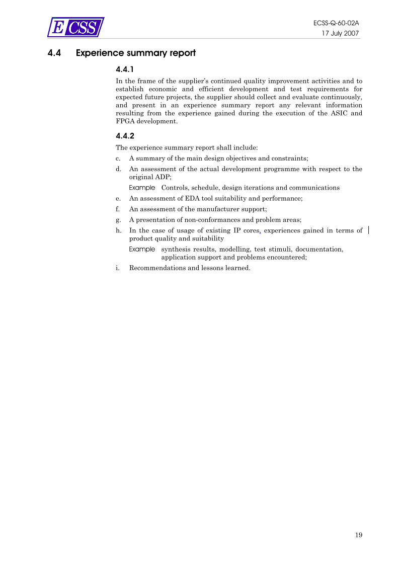
4.4 Experience summary report
4.4.1 In the frame of the supplier’s continued quality improvement activities and to establish economic and efficient development and test requirements for expected future projects, the supplier should collect and evaluate continuously, and present in an experience summary report any relevant information resulting from the experience gained during the execution of the ASIC and FPGA development.
4.4.2 The experience summary report shall include: c. A summary of the main design objectives and constraints; d. An assessment of the actual development programme with respect to the
original ADP; Example Controls, schedule, design iterations and communications
e. An assessment of EDA tool suitability and performance; f. An assessment of the manufacturer support; g. A presentation of non-conformances and problem areas; h. In the case of usage of existing IP cores, experiences gained in terms of
product quality and suitability Example synthesis results, modelling, test stimuli, documentation,
application support and problems encountered; i. Recommendations and lessons learned.

20
17 July 2007 ECSS-Q-60-02A
(This page is intentionally left blank)
21
17 July 2007
ECSS-Q-60-02A
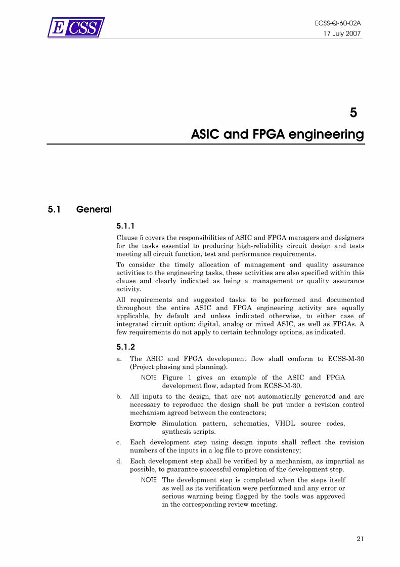
5
ASIC and FPGA engineering
5.1 General
5.1.1 Clause 5 covers the responsibilities of ASIC and FPGA managers and designers for the tasks essential to producing high-reliability circuit design and tests meeting all circuit function, test and performance requirements. To consider the timely allocation of management and quality assurance activities to the engineering tasks, these activities are also specified within this clause and clearly indicated as being a management or quality assurance activity. All requirements and suggested tasks to be performed and documented throughout the entire ASIC and FPGA engineering activity are equally applicable, by default and unless indicated otherwise, to either case of integrated circuit option: digital, analog or mixed ASIC, as well as FPGAs. A few requirements do not apply to certain technology options, as indicated.
5.1.2 a. The ASIC and FPGA development flow shall conform to ECSS-M-30
(Project phasing and planning). NOTE Figure 1 gives an example of the ASIC and FPGA
development flow, adapted from ECSS-M-30. b. All inputs to the design, that are not automatically generated and are
necessary to reproduce the design shall be put under a revision control mechanism agreed between the contractors; Example Simulation pattern, schematics, VHDL source codes,
synthesis scripts. c. Each development step using design inputs shall reflect the revision
numbers of the inputs in a log file to prove consistency; d. Each development step shall be verified by a mechanism, as impartial as
possible, to guarantee successful completion of the development step. NOTE The development step is completed when the steps itself
as well as its verification were performed and any error or serious warning being flagged by the tools was approved in the corresponding review meeting.

22
17 July 2007 ECSS-Q-60-02A
Figure 1 Development flow (example)

23
17 July 2007
ECSS-Q-60-02A
Figure 1 Development flow (example) – continued

24
17 July 2007 ECSS-Q-60-02A
5.2 Definition phase
5.2.1 General The aim of this development step is to establish an ASIC and FPGA requirements specification, a feasibility and risk analysis report and an ASIC and FPGA development plan. The supplier shall ensure that all relevant system configurations and characteristics and all issues imposing requirements on the device are used.
NOTE This allows settling out without any ambiguity the definition status of the collected requirements and verifying that all necessary resources for the design activities are available.
5.2.2 Identification of ASIC and FPGA requirements The supplier shall identify a complete set of traceable ASIC and FPGA requirements which shall be documented in form of an ASIC and FPGA requirements specification (ARS), covering, as a minimum, the following items: a. Overall system partitioning, system configurations and operating modes; b. Interfaces of the ASIC and FPGA to the system and communication
protocols to external devices, including memory mapping; c. Operating frequency range; d. Electrical constraints (e.g. voltage and current supply, drive capabilities
and external load); e. Functional requirements; f. Applicable algorithms; g. Power-up and initialization state; h. Reset and power cycling requirements; i. Error handling; j. Test modes: system and device tests, on ground and in flight; k. Fault coverage required at production test; [only applicable for digital
ASIC designs] l. Timing of critical signals; m. Radiation environment constraints; n. Thermal environment constraints; o. Power budget and dissipation; p. Physical and mechanical constraints: pin assignment, size, encapsulation; q. Reusability or additional functions for future applications; r. Portability to different or newer technologies; s. Intellectual property rights of the design to be developed; t. Proprietary designs (IP cores) to be used as building blocks of the design to
be developed, if already identified.
5.2.3 Feasibility and risk assessment
5.2.3.1 Feasibility study
a. The feasibility of the intended ASIC and FPGA development shall be assessed against the established ASIC and FPGA requirements specification and the available resources.

25
17 July 2007
ECSS-Q-60-02A
b. As a minimum, the following tasks shall be performed and documented: 1. Estimate design complexity; 2. Estimate power consumption; 3. Assess feasibility of speed requirements by a preliminary timing
analysis; 4. Select a radiation hardening approach that ensures compliance with
radiation tolerance requirements. Determine a rough estimate of impact on chip area and circuit speed;
5. Select a production test approach and its feasibility against all requirements;
6. Identify and evaluate the suitability and qualification status of the ASIC technologies or FPGA available to implement the device, fulfilling all functional and non-functional requirements including the specified derating factors. Make a baseline selection;
7. Identify packages, fulfilling all requirements. Make a baseline selection;
8. Ensure that the baseline technology and package or FPGA have a remaining lifetime, so that flight and compatible prototype parts can be manufactured and are available during the expected procurement phase(s);
9. Ensure that technical support for the device can be guaranteed during the expected lifetime;
10. Determine availability and status of the required design and test tools (HW & SW) and libraries;
11. Determine availability of the necessary human resources; 12. Determine availability, licensing, support, legal and economical aspects
of using IP cores from third parties; 13. Ensure that no patents are infringed or agreements exist or can be
made with the patent holder.
5.2.3.2 Risk analysis
a. As a tool of the quality assurance system (see subclause 6.3) a risk analysis shall be performed that identifies potential risk items and assigns preventive measures and contingency plans,
b. The risk analysis shall cover as a minimum the following items: 1. Assurance that the collected ASIC and FPGA requirements are
complete, settled and unambiguous; 2. Maturity of envisaged ASIC or FPGA manufacturers and possible
technologies; 3. Experience and familiarity of engineering resources with the design
type, tools, technology and the potential foundries; 4. Risk of underestimation of design and verification effort; 5. Risk of underestimation of debug and repair efforts; 6. Risk of overestimation of actual gate capacity and clocking frequency; 7. Risk of undetermined I/O behaviour during power-up.
c. This study shall result in a feasibility and risk analysis (FRA) report. NOTE The FRA provides a judgement on the feasibility of the
ASIC and FPGA development as defined by the ASIC and FPGA requirements specification, as well as an assessment of the risks involved.

26
17 July 2007 ECSS-Q-60-02A
5.2.4 ASIC and FPGA development plan a. According to the strategy and approaches specified in subclause 4.2(ASIC
and FPGA control plan), a detailed ASIC and FPGA development plan (ADP) shall be prepared, documented and maintained.
NOTE The purpose of the ADP is to implement the proposed development strategy by identifying all phases of the ASIC and FPGA development with the major activities therein, the project external interfaces and constraints, the design flow, resources (equipment, software and personnel), the allocation of responsibilities, outputs to be produced and, finally, a schedule with milestones, decision points, type and number of design reviews.
b. The ADP shall ensure prospective design portability for devices with long term availability or multiple usage requirements.
c. The ADP shall include, as a minimum: 1. Name of the ASIC and FPGA and its basic function; 2. References to the design documentation and other applicable and
reference documents NOTE Internal and external standards, procedures or coding
guidelines). 3. Development team and assignment of major responsibilities; 4. The baseline FPGA device or ASIC technology including baseline
radiation hardening and testability approach; 5. Companies involved (foundry, subcontractors, suppliers), indicating
their assigned tasks, technical and administrative interfaces; 6. Versions and platforms of tools to be used, including the foundry or
vendor specific tools; 7. Statement for the availability of each design tool (at the site as well as
the dedication to the particular development) 8. The design flow; Example Design entry, synthesis, simulation and verification,
layout generation and verification, production tests and validation.
9. Identification of a configuration management system (see ECSS-M-40); 10. Identification of a verification and validation scheme (see ECSS-E-
10 Part 1B subclause 4.7); 11. The subdivision of the ASIC and FPGA development into reasonably
sized work packages (see ECSS-M-10); 12. The schedule of the ASIC and FPGA development, with estimated
effort and duration of each work package and the planned dates of milestones and review meetings;
13. Identification and full description, including formats, of all relevant outputs, deliverable or not, to be produced along the ASIC and FPGA development (documentation, simulation and test results, test boards, test samples, source or generated codes and programs) and measures intended to achieve best design quality (e.g. HDL coding conformity to an appropriate set of coding rules).

27
17 July 2007
ECSS-Q-60-02A
5.2.5 System requirements review The definition phase is concluded by the system requirements review (SRR) meeting (see quality assurance subclause 6.2), where the documentation generated within this phase shall be reviewed as follows: a. Check that the development activity as defined in the ADP is feasible
within the limits imposed by the project requirements, resources, schedule and budgetary constraints.
b. Check that contingency plans exist for all identified open issues and risk items and that the risk analyzed can be taken for starting the Architectural Design phase.
c. Check that ARS and FRA are complete and documented in a level of detail that avoid any ambiguity for the Architectural Design and all subsequent design work.
d. Check that ARS and FRA include as a minimum: 1. Summary of the system architecture and all expected configurations in
which the device can be used; 2. Specify the external devices connected to the chip and their interface
protocols; 3. Bit numbering and naming convention (to be maintained throughout
the design flow); 4. Format of data structures; 5. Functionality in all nominal operational modes; 6. Functionality for error handling; 7. Functionality in all system test modes; 8. Internal communication protocols; 9. Signal processing algorithms; 10. Definitions of programmable memory elements and their state after
reset; 11. Functional partitioning, establishing a high-level block diagram; 12. Preliminary architectural and HW/SW partitioning, including external
and internal memory mapping; 13. For components providing software programmability, associated
software requirements shall be specified; 14. State and behaviour of l/Os during and after reset and power-up; 15. State functions explicitly not implemented in the design, in order to
avoid potential misunderstandings; 16. Pin list, including power supply and test pins, if already known. The
pin list shall include name, polarity, bus width, interface protocol; 17. Electrical specifications (maximum ratings, AC, DC and timing
diagrams); 18. Power dissipation estimates for main functional modes; 19. Operating conditions (supply, temperature, radiation); 20. Baseline package and pin-out, if already known.
EXPECTED OUTPUTS: a. the definition phase documentation, containing:
1. ASIC and FPGA requirements specification (ARS);
2. Feasibility and risk analysis (FRA);
b. ASIC and FPGA development plan (ADP);
28
17 July 2007 ECSS-Q-60-02A
c. MoM of SRR.
5.3 Architectural design
5.3.1 General a. During the architectural design phase, the architecture of the chip shall be
defined, verified and documented down to the level of basic blocks implementing all intended functions, their interfaces and interactions.
b. Important selections for the implementation of the chip shall be made or confirmed.
c. All definitions and selections made shall conform to the definition phase documentation.
d. Any deviation shall be justified in the preliminary design review. e. The architecture definition and the baseline choices made during the
definition phase shall be settled, frozen and documented with a level of detail that allows proceeding with the subsequent detailed design.
5.3.2 Architecture definition a. As a minimum the following tasks shall be performed and documented in
an architecture definition report: 1. Subdivide the chip into its fundamental functions or blocks, identifying
and thoroughly documenting their interfaces, functionalities and interactions.
2. Define the architecture down to the level required to implement technology specific, transistor- or gate-level mapping;
3. Select suitable algorithms and circuit schemes including their parameters to implement the identified functions;
4. Identify sub-functions, which can be used as an individual block at different locations of the chip or possibly be compiled as a core for other designs;
5. Identify a suitable clocking and reset scheme assuring correct transitions of data between clock domains and identify asynchronous parts of the design;
6. Select (if not yet done), IP-cores to be used or previously designed units to be re-used in the design. Procure and verify them. NOTE This verification can be done by test cases provided by the
IP core vendor, by test benches from an independent source, or by newly designed test programs.
7. If the verification is accomplished during prior instantiations of the core, assess it for covering the actual system environment, and eventually bug-fixes and workarounds or additional verification shall be performed;
8. Identify and eventually procure custom cells, to be used in the design, verify the consistency of the different models delivered (e.g. simulation models, layout and timing view);
9. Generate models required as an input to the subsequent detailed design phase (e.g. synthesizable RTL models); NOTE There is no firm requirement for intermediate behavioural
simulations, nor for any model being coded in a particular language or a specific level of abstraction. However, the coding of behavioural models of critical functions and

29
17 July 2007
ECSS-Q-60-02A
algorithms is strongly encouraged, since they frequently are valuable tools for further verification tasks.
b. The architecture definition report shall include the architecture broken down to the selected blocks, their interfaces, functionality or algorithms and interactions.
c. Even though the chip and its architecture is completely described in a simulation model (executable specification), a detailed text specification shall be edited.
5.3.3 Verification plan a. The supplier shall establish a verification plan
NOTE The verification plan defines how the functionality and non-functional requirements stated in the definition phase documentation are demonstrated at all levels of modelling, starting from the behavioural level down to the gate level.
b. As a minimum the following items shall be addressed and verified: 1. In the case of complex digital ASIC developments, verification by FPGA
prototyping or emulation; 2. Requirements for code coverage in digital designs; 3. Requirements for HW-SW interaction, possibly by performing co-
simulation; 4. Application of coding rules.
5.3.4 Architecture verification and optimization As a minimum, the following activities shall be performed and documented in an architecture verification and optimization report: a. Verify that the defined architecture meets the requirements by appropriate
simulation and analysis techniques; b. The models referred to in subclause 5.3.2 item f 9 above shall be verified
according to the verification plan. An independent verification shall be performed to avoid masking of design errors;
c. When allocation and connectivity of hard-macro cells can be an issue, a preliminary floorplan shall assure that the expected cells are effectively place- and routable within the given constraints; [not applicable for FPGA designs]
d. Re-assess the feasibility and risks; e. For conflicting requirements (such as power consumption vs. speed and
performance, pin count vs. package size and complexity vs. die area) an application related trade-off shall be found and the implementation choices shall be established.
5.3.5 Preliminary data sheet A preliminary data sheet shall be produced, to be updated and completed at the end of the ASIC and FPGA development (see 7.4.1 for details).
5.3.6 Preliminary design review The architectural design phase is concluded by the preliminary design review (PDR) meeting (see quality assurance subclause 6.2), where the documentation generated within this phase shall be reviewed as follows: a. Check that the selected trade-off meets the requirements fixed during the
definition phase;

30
17 July 2007 ECSS-Q-60-02A
b. Check that preventive measures or contingency plans exist for all identified risk items and that the risk analyzed can be taken for starting the detailed design;
c. Check that the architectural design documentation (see 7.3.3) together with the documentation of previous development phases is complete, traceable and documented in a level of detail that allow to proceed with the detailed design;
d. Identify, justify and approve discrepancies between the architectural design documentation and the definition phase documentation;
e. Check that the planned measures, tools, methods and procedures are applied.
EXPECTED OUTPUTS: a. Architecture definition report;
b. Verification plan;
c. Architecture verification and optimization report;
d. Preliminary data sheet;
e. Design database, containing:
1. Simulation models;
2. Verification results;
f. MoM of PDR.
5.4 Detailed design
5.4.1 General During this phase the high-level architectural design is translated into a structural description on the level of elementary cells of the selected technology and library. Additional information is generated for the subsequent development phases, such as layout constraints, floorplanning, production test programs and a detailed pin description. For digital designs, the above mentioned design description is the associated technology specific, verified gate-level pre-layout netlist, whereas for analog designs, it is a verified sized transistor-level netlist. However, in many analog designs, there is no separation between circuit design and layout. a. Influences from layout such as cross talk and matching shall be accounted
for during the design work. b. For analog designs circuit and layout are developed concurrently, and the
reviews for detailed design and layout phases may be held together. c. For FPGAs and analog designs, a combined DDR and CDR meeting may be
justified. NOTE In these cases also the corresponding output reports can
be merged together. d. The scripts used for an automatic and repeatable generation shall be part
of the design database. NOTE 1 The main output of the detailed design is a design
database, which contains, or allows an automatic and repeatable generation of the above-mentioned inputs to the layout;
NOTE 2 The scripts defined for this generation are an essential part of the detailed design,

31
17 July 2007
ECSS-Q-60-02A
5.4.2 Design entry During the design entry the following tasks shall be performed and documented in a design entry report: a. Use the agreed design tools as specified in the ADP (see 5.2.4). Check their
maintenance status, consider known bugs, existing patches, preventive and workaround measures;
b. Implement the specified test concept during design entry and synthesis (e.g. scan paths, DFT logic, measurement points, test busses and boundary scan (JTAG, see IEEE 1149.1);
c. Implement the specified radiation hardening concept by design and during synthesis;
d. Continuously verify the results by the appropriate methods, as specified in the verification plan;
e. Determine a pin-out and bonding scheme with particular attention to the technical constraints such as power supply(ies) pin definition and bondability issues;
f. Select buffers according to the I/O requirements defined in the ASIC and FPGA requirements specification;
g. Establish or refine the floorplan; [not applicable for FPGA designs].
5.4.3 Netlist generation a. In this step, the source description of the design is translated into the
netlist, and any other information required for the layout generation, such as floorplan or placement information and constraints for timing driven layout is generated.
b. Enough iterations between design entry, netlist and layout generation shall be performed in order to accomplish the design requirements,
c. Iterations back to the architectural design shall be avoided. d. If an iteration back to the architectural design is required by means of
changes in the model released during the PDR, that model shall be verified again.
e. As a minimum the following tasks shall be performed and documented in a netlist generation report: 1. Consider the required derating factors; 2. Ensure that the appropriate library cells are used as to fulfil all the
requirements collected in the ASIC and FPGA requirements specification;
3. Select or generate appropriate models for parasitics (e.g. wire load models); [not applicable for FPGA designs];
4. Perform a design parameter centring; [only applicable for analog ASIC designs];
5. Ensure that the intended operating (process, voltage, temperature) and environment (radiation) conditions are used during the translation and verification exercise;
6. If synthesis tools are used, generate scripts which allow performing the fully automatic pre-layout netlist generation in a repeatable way;
7. These scripts being part of the inputs to the design, shall also follow the general requirements for e.g. documentation, commenting and version control;
8. Specify timing constraints, and vendor-specific design rules;
32
17 July 2007 ECSS-Q-60-02A
9. Consider over-constraining to anticipate parasitic effects.
5.4.4 Netlist verification As a minimum the following tasks shall be performed and documented in a netlist verification report: a. Verify the netlist according to the verification plan; b. Verify the estimated data for the layout parasitics and delays; c. Perform gate level simulations, using the complete test suite from the
architectural design, or an equivalent set of methods, such as formal verification and static timing analysis; [not applicable for analog ASIC designs];
d. Verify key parameters, such as bias voltages, operating point, frequencies, bandwidth, matching, s-parameters, noise, dynamic and linear ranges and shaping times;
e. A functional verification shall be obtained, including the interfaces. [only applicable for analog ASIC designs];
f. If a complete simulation of all modes (including test modes) at top level cannot be performed (e.g. due to run-time restrictions), simulate a representative subset;
g. Verify by an extrapolating analysis, the not simulated cases; h. Verify that the specified test concept is implemented through e.g. scan
paths, DFT logic, measurement points and test busses; i. Verify that the radiation-hardening concept is successfully included in the
netlist. Consider e.g. netlist inspection and SEU injection simulations; j. Verify that the specified power consumption is respected; k. Update relevant parameters in the preliminary data sheet according to the
results obtained during the verification; l. If production tests or a pre- and post burn-in test are planned, generate the
test vectors and verify the requirements for fault coverage; m. For IP cores and macro cells: include the core's test patterns in the overall
ASIC's test programmes; n. Verify, that the pre-layout vendor design rules are met and assess the
relevance of violations; [not applicable for FPGA designs] o. Perform a parameter sensitivity analysis; [only applicable for analog ASIC
designs].
5.4.5 Updated data sheet The supplier shall update the data sheet to incorporate the new established information on for instance pinout and estimated timing.
NOTE For further details see 7.4.1.
5.4.6 Detailed design review The detailed design phase is concluded by the detailed design review (DDR) meeting (see 6.2), where the documentation generated within this phase shall be reviewed as follows: a. Check that the detailed design documentation (see 7.3.4) together with the
documentation of previous development phases completely documents all results obtained and decisions made along with the corresponding justifications in a level of detail that allow to proceed with the layout. This shall include as a minimum:

33
17 July 2007
ECSS-Q-60-02A
1. Circuit implementation: Describes details of the implementation, which were not specified during architectural design;
2. Description of implemented testability and production test methods including the achieved fault coverage figures obtained;
3. Description of implemented radiation hardening measures; 4. All verification results; 5. Description of cells specially developed for the design; 6. Configuration and modifications applied to IP cores used in the design; 7. List of items with name and format provided to the foundry (i.e. netlist,
stimuli files for production test and constraints files); [not applicable for FPGA designs];
8. Description of the design database, including the file structure, naming conventions, version control labels, netlist generation methods and constraints;
9. All tools and ASIC libraries actually used during the entire design development, including the versions and operating platforms used;
10. Problems encountered with design tools and their workarounds. b. Check that the planned measures, tools, methods and procedures were
applied; c. Check that the outputs are in conformance to the requirements fixed
during the definition phase; d. In particular, when the layout is performed by another company (foundry),
assess specific foundry requirements (netlist sign-off criteria).
EXPECTED OUTPUTS: a. Design entry report;
b. Netlist generation report;
c. Netlist verification report;
d. Updated data sheet with pin-out;
e. Updated design database, containing:
1. Pre-layout netlist;
2. Constraints for layout (i.e. floorplan and constraints for timing driven layout) as defined in the ADP;
3. Test vectors for production test;
f. MoM of DDR.
5.5 Layout
5.5.1 General a. The layout shall generate the placement and routing information to meet
the design rules, timing and other constraints. b. In addition, netlist optimization by local re-synthesis or physical synthesis
shall be applied NOTE This provides reliable information about loads and
coupling capacitors and the final design rule check that assures a verified netlist which can be forwarded to the foundry.

34
17 July 2007 ECSS-Q-60-02A
5.5.2 Layout generation As a minimum the following tasks shall be performed and documented in a layout generation report: a. finalize the floorplan of the chip; [not applicable for FPGA designs]; b. perform place and route (P&R) taking into account all layout constraints; c. perform netlist optimizations (see 5.5.1) for timing and design rules if
necessary; [only applicable for digital ASIC designs]; d. generate the power distribution; e. generate the clock distribution (clock tree and buffers); [not applicable for
analog ASIC designs]; f. insert core and pad ring power distribution and possibly additional test
pads in the circuit; g. determine the die size; [not applicable for FPGA designs]; h. generate the bonding diagram respecting bonding and package constraints;
[not applicable for FPGA designs]; i. generate the input data for mask or programming file generation (IDMP).
5.5.3 Layout verification As a minimum the following tasks shall be performed and documented in a layout verification report: a. layout design rule check (DRC); b. electrical rule check (ERC), check cross-talk sensitivity, if required by
customer; c. extract a netlist from the layout given in terms of IDMP; d. verify that the gate-level netlist is consistent with the layout by
performing a layout versus schematic (LVS) comparison, i.e. a netlist comparison check (NCC) between the post-layout netlist and the layout (IDMP) extracted netlist;
e. verify that the post-layout netlist is consistent in terms of functionality with the pre-layout netlist by simulation and formal methods;
f. extract the parasitic information; NOTE This delivers capacitance, resistance and inductivity
values (only deep sub-micron technology), from which the actual delays are calculated for digital designs;
g. perform comprehensive post-layout verification according to the verification plan;
NOTE This is mostly accomplished by back-annotated simulations and timing analysis;
h. check the resulting clock skew and latency; [not applicable for FPGA designs]
i. check relevant timing of I/Os; j. check the power distribution on the chip; [not applicable for FPGA designs] k. perform transition check and load check on the nets inside the ASIC; l. characterize ASIC and FPGA timing performances,
Example Such as max clock frequency, clock duty cycle, set-up and hold times for all inputs and propagation delays for all outputs.

35
17 July 2007
ECSS-Q-60-02A
5.5.4 Design validation plan a. The supplier shall establish and maintain a design validation plan (DVP)
NOTE The purpose of the design validation plan is to specify the measurements that are performed on the prototypes in order to verify that the new implemented devices contain the functionality and the characteristic they are designed for.
b. According to the approaches specified in the ADP (see 5.2.4), the DVP shall include as a minimum: 1. description and requirements for the test set-up or system breadboard; 2. operating modes and test conditions of the prototypes under test; 3. characteristics and functions to be validated and checked against the
ASIC and FPGA requirements specification; 4. if a radiation test is required by the customer, the corresponding
radiation verification test plan.
5.5.5 Updated data sheet The supplier shall update the parameters in the data sheet according to the results obtained during the layout verification.
NOTE For further details see 7.4.1.
5.5.6 Draft detail specification Based on the information collected in the design documentation a draft detail specification shall be established according to the requirements given in 7.4.3.
5.5.7 Critical design review The layout phase is concluded by the critical design review (CDR) meeting (see 6.2), where the documentation generated within this phase is reviewed: a. The layout documentation (see 7.3.5) together with the documentation of
previous development phases completely documents the progress and decisions made during the layout shall be checked
b. As a minimum, the review of the documentation at CDR shall address: 1. Post-layout clock distribution tree and clock skew and latency analysis; 2. Post-layout verification results and analysis of timing margins; 3. Results from all layout checks (e.g., DRC, ERC, LVS and NCC) Any
violation of or deviations from the design rules and justifications. c. The reviewers shall check that the planned measures, tools, methods and
procedures have been applied; d. The reviewers shall check that the outputs are in conformance to the
requirements fixed during the definition phase; e. In the case where no DDR was held after the detailed design phase, the
reviewers shall check that the CDR encompasses also all review items of the DDR;
f. The reviewers shall check that preventive measures or contingency plans exist for all identified risk items and that the risk analysed can be taken for starting the Prototype Implementation;
EXPECTED OUTPUTS: a. Layout generation report;
b. Layout verification report;
c. Design validation plan;

36
17 July 2007 ECSS-Q-60-02A
d. Updated data sheet;
e. Updated design database, containing:
1. Post-layout netlist in the agreed format depending on the targeted technological approach (GDS II, FPGA P&R files or other);
2. Corresponding parasitic information;
f. MoM of CDR.
5.6 Prototype implementation
5.6.1 General In this phase chips are manufactured and packaged, or FPGA's programmed, and the prototypes are tested.
NOTE In the following, the term production refers to chip manufacturing and packaging, or FPGA programming, whatever is applicable. The phase is concluded by the delivery of the tested devices.
5.6.2 Production and test As a minimum, the following tasks are performed and documented in a production test report: a. The package shall be the same as for flight devices, if required by the
customer; b. The mask generation and verification shall be performed under the
foundry's configuration control system; [not applicable for FPGA designs] c. The committed number of prototypes shall be produced and delivered, so
that design validation can be performed; d. The production test shall be performed on 100 % of the delivered
prototypes, using the test vectors generated during the previous phases. e. The production test shall demonstrate that the device was produced
correctly. [not applicable for FPGA designs] f. The correctness of the FPGA programming shall be verified (checksum
test). [only applicable for FPGA designs] g. The tested parameters and conditions shall be according to the draft detail
specification (see 7.4.3); h. Test reports shall be generated and delivered, documenting the measured
parameters. Tester log files shall be delivered in electronic format;
EXPECTED OUTPUTS: a. Agreed number of tested devices (ASICs or FPGAs);
b. Production test results and reports; [not applicable for FPGA designs]
c. Burn-in or any other production test results, specifications and patterns;
5.7 Design validation and release
5.7.1 Design validation a. The design validation shall be performed to confirm the achievement of all
functional, performance, interface and compatibility requirements.

37
17 July 2007
ECSS-Q-60-02A
b. As a minimum, the following tasks shall be performed and documented in a validation report: 1. carry out the validation according the established validation plan; 2. design and build the test set-up or system breadboard in order to
represent a realistic system application; 3. use the breadboard to perform validation tests that cover full
functionality and all operating modes and conditions of the device; 4. if contractually agreed, specify, design and execute specific burn-in or
other screening tests for the later test of the FM parts; 5. document scope, sequences, set-up and results of the validation tests in
the validation report NOTE The validation report becomes part of the design
validation documentation. 6. Compare specified parameters with measured parameters.
c. The validation report shall be made available to the foundry and the design house.
5.7.2 Radiation test performance a. The device prototypes shall undergo radiation testing according to the
requirements of the project, if the required hardening level is not yet demonstrated for the technology involved.
b. Radiation testing shall be performed according to the established radiation verification plan included in the design validation plan and documented in a radiation test report.
5.7.3 Design release and FM production preparation For the design release and FM production preparation, the following requirements are fulfilled and documented in a release report: a. License agreements for the intellectual property (the design itself and
third party IP cores) contained in the device shall be established to cover the whole lifetime.
b. The supplier shall ensure technical support of the device during the lifetime of the product.
NOTE This can be accomplished through a know-how transfer from the design house to the foundry or a third party, or by the design house itself.
c. The suppler shall ensure the storage of the complete design database during the lifetime of the product, including associated data, documentation, pattern generation files, test program(s) and mask sets used.
d. In the case of using non-QML manufacturer or foundry, an evaluation programme (see ECSS-Q-60) shall be performed that include as agreed by the customer the following activities: — manufacturer evaluation; — constructional analysis; — evaluation testing.
e. On completion of the evaluation programme additional data such as reliability and radiation data shall be available ensuring that the mission requirements can be met.
f. The supplier shall assess the risk involved for the FM production.

38
17 July 2007 ECSS-Q-60-02A
5.7.4 Experience summary report This activity is a management task that is described in this subclause because of schedule reasons. The purpose of the experience summary report is to collect the experience gained during the execution of the ASIC and FPGA procurement programme as detailed in subclause 4.3
5.7.5 Final versions of application and procurement documents
a. The detail specification (see subclause 7.4.3) and, if requested by the customer, the data sheet (see subclause 7.4.1) shall be updated based on the validation test results.
b. The data sheet, eventually transformed to the foundry specific format, shall be available during the device lifetime.
c. An application note (see 7.4.2) shall be established.
5.7.6 Qualification and acceptance review The design validation phase is concluded by the qualification and acceptance review (QR/AR) meeting (see 6.2), where the documentation generated within this phase are reviewed as follows: a. The reviewer shall check that the design validation documentation (see
7.3.5) together with the documentation of previous development phases is complete;
b. The reviewer shall check that the device achieves functional, performance, interface and compatibility characteristics satisfying the ASIC and FPGA requirements specification;
c. The reviewer shall check that the planned measures, tools, methods and procedures were applied;
d. The reviewer shall check that preventive measures or contingency plans exist for all identified risk items and that the risk of FM production can be taken.
EXPECTED OUTPUTS: a. Validation report;
b. Radiation test report (if applicable);
c. Release report;
d. Experience summary report;
e. Final data sheet;
f. Final detail specification;
g. Application note;
h. MoM of QR/AR;
i. Validation breadboard;
j. Burn-in or screening test boards for FM parts
39
17 July 2007
ECSS-Q-60-02A
6
Quality assurance system
6.1 General The quality assurance requirements defined in: a. ECSS-Q-20B subclause 4.4 (QA status reporting) shall apply, b. ECSS-Q-30B subclause 6.4 (criticality classification of functions and
products) shall apply, c. ECSS-Q-60B subclauses 4.5, 5.5 and 6.5 (components quality assurance)
shall apply. NOTE The objective of the quality assurance system is to ensure
the development of reliable, manufacturable, testable and reproducible, custom designed components for space application.
d. The tools to be used shall be specified and approved by the customer. e. All technology independent CAD tools to be employed during the
development shall be mature and fit for their purpose. f. All technology dependent CAD tools shall be used as approved and
supported by the selected manufacturer. g. Preference shall be given to the use of established international standards,
such as VHDL as defined in IEEE 61691-1-1 and EDIF.
6.2 Review meetings a. The supplier shall schedule and conduct design reviews (see
ECSS-M-30-01). b. Design reviews shall be defined along with the criteria for their successful
completion in the ASIC and FPGA development plan (see 5.2.4). c. Representation, for design and quality assurance, from all relevant
organizations (customer, system contractor, design house and foundry) shall be ensured.
d. The supplier shall produce and circulate in advance of each design review a design review package containing a checklist based on the established requirements and the data necessary for the particular review.

40
17 July 2007 ECSS-Q-60-02A
e. The following reviews shall be performed: 1. System requirements review (SRR)
NOTE This review results in the authorization to start the
architectural design. The outputs reviewed and the items checked are detailed in 5.2.5.
2. Preliminary design review (PDR)
NOTE PDR results in the authorization to start with the detailed design. The outputs reviewed and the items checked are detailed in 5.3.6.
3. Detailed design review (DDR) (if applicable) NOTE 1 DDR results in the authorization to proceed with the
layout. The outputs reviewed and the items checked are detailed in 5.4.6.
NOTE 2 In the case the design and layout is a concurrent or interdigitated activity (for instance analog or FPGA design) this review meeting can be combined with the subsequent CDR meeting.
4. Critical design review (CDR) NOTE CDR results in the approval of design and layout and the
release for prototype implementation. The outputs reviewed and the items checked are detailed in 5.5.7.
5. Qualification and acceptance review (QR/AR) NOTE QR/AR results in the final acceptance of the design and
the release for FM production. The outputs reviewed and the items checked are detailed in 5.7.6.
6. Additional design reviews as agreed by the contractors. f. Direct or delegated customer participation and manufacturer or foundry
participation for CDR and QR/AR shall be mandatory NOTE 1 The decision on a successful completion of a review
meeting can only be achieved by consent of all parties. NOTE 2 A review identifying a limited number of only minor
discrepancies can be completed after successful implementation of the corrective actions defined during the review.
g. A review failing major acceptance criteria and resulting in a design iteration shall be repeated in full.
h. The criteria for a successful review meeting shall be defined prior to the relevant meeting.
NOTE These criteria can be defined on the preceding review meeting.
i. All review meetings shall be minuted. j. The MoMs of the review meetings shall be added to the management
documentation

41
17 July 2007
ECSS-Q-60-02A
6.3 Risk assessment and risk management a. The design risk for the timely and successful completion of the
development activity shall be assessed according to the items listed in 5.2.3.2.
b. Risk assessment shall be performed concurrently to the design activity. c. Extraordinary risks shall be covered by a contingency plan identifying
alternative or back-up solutions. d. A check of the risk mitigation activities shall be a major item of the agenda
of every review meeting.

42
17 July 2007 ECSS-Q-60-02A
(This page is intentionally left blank)
43
17 July 2007
ECSS-Q-60-02A
7 Development documentation
7.1 General a. At all stages of the ASIC and FPGA development, the supplier shall
produce, maintain, control and archive all related documentation as defined and detailed in the following paragraphs.
b. The documentation shall be well structured and easily readable, so that the design can be understood by other ASIC and FPGA designers of the supplier and manufacturer not permanently involved in the design work. Example Names of signals and blocks are chosen to indicate their
function. c. One consistent language shall be used throughout the documentation,
preferably English. d. The documentation shall be consistent, e.g. the same item have the same
name in all documentation. e. Block diagrams, control flow charts, timing diagrams and other figures
shall be introduced where beneficial for the understanding of the text. f. Every time an updated document is delivered, it shall include a detailed
change list, and all significant changes marked using a change bar in the margin.
g. If a document is delivered before being complete, each page with incomplete information shall be clearly marked.
NOTE Some of the information listed is better delivered separately or in appendices, such as layout plots, gate-level schematics and lists of undetected faults.
h. All documents shall be archived for a minimum period of five years after completion of the development activity or as agreed by the customer.
7.2 Management documentation The management documentation shall provide the overall strategy for the development activity including task planning and organization and approaches, methods and applicable procedures.
NOTE The management documentation also includes the status reporting as MoM of the review meetings and an assessment of the experience gained during the development activity. The management documentation is a gathering of separate documents (see subclauses 4.2, 4.4, 5.2.4, 5.3.3, 5.5.4, 6.2).

44
17 July 2007 ECSS-Q-60-02A
7.3 Design documentation The purpose of the design documentation (DD) is to record the progress achieved and the decisions made along with the corresponding justifications during the development phases of the device. a. All design information shall be stored in a design database by applying the
contractual agreed revision control mechanism (see 5.1). b. All intermediate design data shall be reproducible to assist possible
iterations. c. As the design database consists of electronic data that cannot be reviewed
directly, formless reports shall be established that contain a legible extract of the database.
d. Reports that shall be produced during the individual phases of a development activity are detailed in Clause 5.
NOTE An example of a suitable filing of this design documentation is given in Figure 2.
NOTE In the case the design and layout is a concurrent or interdigitated activity (e.g. analog and FPGA design) the corresponding output reports can be merged together.

45
17 July 2007
ECSS-Q-60-02A
Figure 2 Design documentation
Definition phase Documentation
A/F requirements specification Feasibility and Risk Analysis
Architectural Design Documentation
Architecture Definition Report Verification and Optimization Report
Detailed Design Documentation
Design Entry Report Netlist Generation Report Netlist Verification Report
Layout Documentation
Layout Generation Report Layout Verification Report
Design Validation Documentation
Validation Report Radiation Test Report (if applicable)
Release Report

46
17 July 2007 ECSS-Q-60-02A
7.3.1 Definition phase documentation The definition phase documentation consists of the following contributions: a. The ASIC and FPGA requirements specification (ARS) shall be established
during the first development phase. b. ARS shall include a complete set of ASIC and FPGA requirements, as
detailed in 5.2.2, that are settled, unambiguous and frozen. c. The feasibility and risk analysis (FRA) shall be assessed with regards to
the following drivers: • consistency and quality of the ASIC and FPGA, • system requirements feasibility of the ASIC and FPGA
development, • estimate of the risk involved. NOTE The feasibility and risk analysis (FRA) report is the
second part of the definition phase documentation. d. FRA shall cover the items detailed in 5.2.3.
7.3.2 Architectural design documentation The architectural design documentation adds the following contributions to the definition phase documentation: a. The architectural definition report shall include the architecture broken
down to the selected blocks, their interfaces, functionality, algorithms and interactions as specified in 5.3.2.
b. The verification and optimization report shall document the simulations performed, the results received, the trade-offs found and the implementation choices established. Further details are given in 5.3.4.
7.3.3 Detailed design documentation The detailed design documentation adds the following contributions to the architectural design documentation: a. The design entry report shall document all inputs available for the detailed
design phase as detailed in 5.4.2. b. The netlist generation report shall describe the work performed and the
decisions taken to generate a netlist as detailed in 5.4.3. c. The netlist verification report shall list all steps of simulation and
verification performed (see 5.4.4) together with the corresponding results.
7.3.4 Layout documentation The layout documentation adds the following contributions to the detailed design documentation: a. The layout generation report shall describe the work performed and the
decisions taken to generate layout as detailed in 5.5.2. b. The layout verification report shall list all steps of verification performed
(see 5.5.3) together with the corresponding results.
7.3.5 Design validation documentation The design validation documentation adds the following contributions to the layout documentation: a. The validation report shall present the scope, sequences, set-up and results
of the validation tests performed as detailed in 5.7.1.
47
17 July 2007
ECSS-Q-60-02A
b. The radiation test report (if applicable) shall document the test board circuitry and bias conditions, the test sequence and investigated irradiation levels, the performed measurements and the resulting degradations.
c. The release report shall summarize all activities performed to assure that all necessary prerequisites are fulfilled to start a FM production (see 5.7.3).
7.4 Application and procurement documents
7.4.1 Data sheet a. If requested by the customer, a data sheet that describes the functionality
of the device so it can be used by a board or system designer shall be established.
b. Each page shall contain the device name and number and the date of issue. NOTE The first page contain a summary of the device
functionality, a block diagram and short list of features, such as operating frequency, technology and the foundry address.
c. All characteristics and limitations introduced during the design shall be described, such as detailed interface descriptions, register definitions and memory maps.
d. The data sheet shall include a system overview of the device and a description of how to use the device in a representative system environment, including an application block diagram.
e. The full functionality and all operating modes shall be specified in detail. f. All signal interfaces shall be described in detail including for instance a
description of all signals, test and power pins, specifying e.g. the usage of the signals and the signal polarity.
g. The signal descriptions shall be grouped according to their function. h. All electrical and mechanical data shall be specified, together with their
relevant applicable conditions (e.g. temperature and capacitive load), including: 1. Absolute maximum ratings, including storage temperature, operating
temperature, supply voltage, maximum input current for any pin, total dose, single event upset, latch-up, electrostatic discharge and reliability figures;
2. DC parameters, including voltage levels, leakage currents, pin capacitances and output currents;
3. Static and dynamic (per MHz) power dissipation, allowing the power consumption at lower operating frequencies to be calculated, if representative;
4. AC parameters, including e.g. set-up and hold times, cycle periods, output delays and tri-state delays, together with waveform diagrams.
5. Evidences that timing parameters relate to the relevant reference signal edges;
6. Package description, including pin assignment, package figure with pin numbers and preferably signal names, and a mechanical drawing for the package dimensions including information on the thermal characteristic of the package such as wall thickness, thermal coefficient of material or package.
i. A preliminary data sheet shall contain all parts of a final data sheet, with the same level of detail.

48
17 July 2007 ECSS-Q-60-02A
j. When data does not exist , estimates shall be used and clearly indicated to be estimates.
7.4.2 Application note a. If requested by the customer, an application note shall be established for
components that are regarded as standard parts for a variety of system applications.
b. In such a case the application note shall guide the user through the possible configurations the device or module can be operated with.
c. Examples for the corresponding bias circuitry, supply voltages and configuration signals shall be provided.
7.4.3 Detail specification a. All devices intended for use as FM products shall be procured according to
controlled specifications. b. All new specifications shall be designed to be totally in conformance to one
of the existing European standardization systems. c. New detail specifications shall include the following as a minimum:
1. relevant electrical and mechanical parameters; 2. screening, burn-in, and acceptance requirements; 3. deviations from the generic specification; 4. documentation and data requirements; 5. delta limits, when applicable; 6. criteria for percent defective allowable; 7. lot acceptance tests or quality conformance inspections; 8. marking; 9. storage requirements; 10. requirements for lot homogeneity; 11. serialization, when applicable; 12. protective packaging and handling requirements; 13. radiation verification testing requirements, when applicable.
d. Specifications shall include configuration control requirements that ensure that any change of the product that refers to the qualification or that can affect performance, quality, reliability and interchangeability is identified by the manufacturers.

49
17 July 2007
ECSS-Q-60-02A
8 Deliverables
8.1 General a. Upon request, the customer shall receive free of charge from the
manufacturer or foundry, for the duration of the development, a complete design kit for the selected process, including all libraries and design kit tools and their complete documentation, in order to allow the customer to independently verify the design.
NOTE This only applies if such a design kit actually exists for the design tools available at the customer;
b. The quantity to be delivered of each individual deliverable item shall be agreed between customer and supplier according to the requirements of the actual project.
c. Additional items shall be defined as necessary. d. Each delivery of a design document shall be accompanied by a written
statement of the status of the deliverable item. e. The IP rights status shall be reported. f. Paper copies shall be easily readable and suitable for subsequent photo-
copying. Electronic copies shall be submitted via electronic media in an agreed format with agreed characteristics. Example Search capability, printability, usage of hyperlinks,
traceability and changeability. g. Photos and layout plots may be part of the documentation only for
promotional information with restricted details, if not specified elsewhere.
8.2 Deliverable items The list of deliverables is defined per contractually agreed SoW. Table A-1 represents a guideline for documentation, design database deliverables and hardware deliverables that become available during the ASIC and FPGA development.

50
17 July 2007 ECSS-Q-60-02A
(This page is intentionally left blank)

51
17 July 2007
ECSS-Q-60-02A
Annex A (normative) Document requirements list and configuration
items to be delivered
Table A-1 Deliverables of the ASIC and FPGA development
Development phase
Documentation SW HW
A/F control plan
Definition phase A/F requirements specification Feasibility and risk analysis A/F development plan MoM of SRR
Architectural design
Architecture definition report Verification plan Architecture verification and optimization report Preliminary data sheet MoM of PDR
Design database containing: Simulation models Verification results
Detailed design Design entry report Netlist generation report Netlist verification report Updated data sheet MoM of DDR
Updated design database containing: Pre-layout netlist Constraints for layout Test vectors for production
Layout Layout generation report Layout verification report Design validation plan Updated data sheet Draft detail specification MoM of CDR
Updated design database containing: Post-layout netlist Corresponding parasitic information
Prototype implementation
Production test results and reports Burn-in or any other production test results, specification, pattern
Agreed number of tested devices (ASICs or FPGAs)
Design validation and release
Validation report Radiation test report Release report Final data sheet Final detail specification Application note Experience summary report MoM of QR/AR
Validation breadboard Burn-in or screening test boards for FM parts

52
17 July 2007 ECSS-Q-60-02A
(This page is intentionally left blank)

53
17 July 2007
ECSS-Q-60-02A
Bibliography
IEEE 61691-1-1 Behavioural languages Part 1-1: VHDL language reference manual
IEEE 1149.1 Standard Test Access Port and Boundary-Scan Architecture

54
17 July 2007 ECSS-Q-60-02A
(This page is intentionally left blank)

55
17 July 2007
ECSS-Q-60-02A
ECSS Change Request / Document Improvement Proposal A Change Request / Document Improvement Proposal for an ECSS Standard may be submitted to the ECSS Secretariat at any time after the standard’s publication using the form presented below. This form can be downloaded in MS Word format from the ECSS Website (www.ecss.nl, in the menus: Standards - ECSS forms).
ECSS Change Request / Document Improvement Proposal
1. Originator’s name: 2. ECSS Document number:
Organization: 3. Date:
e-mail:
4. Number.
5. Location of
deficiency clause page (e.g. 3.1 14)
6. Changes
7. Justification
8. Disposition
Filling instructions:
1. Originator’s name - Insert the originator’s name and address 2. ECSS document number - Insert the complete ECSS reference number (e.g. ECSS-M-00B) 3. Date - Insert current date 4. Number - Insert originator’s numbering of CR/DIP (optional) 5. Location - Insert clause, table or figure number and page number where deficiency has been
identified 6. Changes - Identify any improvement proposed, giving as much detail as possible 7. Justification - Describe the purpose, reasons and benefits of the proposed change 8. Disposition - not to be filled in
Once completed, please send the CR/DIP by e-mail to: [email protected]

56
17 July 2007 ECSS-Q-60-02A
(This page is intentionally left blank)