Embed Size (px)
Citation preview
978-1-5090-6023-8/17/$31.00 ©2017 IEEE
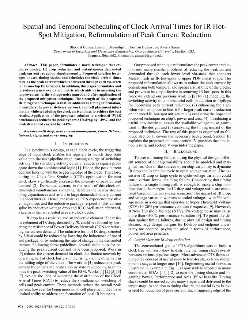
Spatial and Temporal Scheduling of Clock Arrival Times for IR Hot-Spot Mitigation, Reformulation of Peak Current Reduction
Bhoopal Gunna, Lakshmi Bhamidipati, Houman Homayoun, Avesta Sasan Department of Electrical and Electronics Engineering, George Mason University, Fairfax, USA.
{bgunna, lbhamid2, hhomayou, asasan}@gmu.edu
Abstract—This paper, formulates a novel technique that ex-plores on-chip IR drop reduction and instantaneous demanded peak-current reduction simultaneously. Proposed solution lever-ages unused timing slacks, and schedules the clock arrival times to relax the peak current which is delivered through each via-stack in the on-chip IR hot-spots. In addition, this paper formulates and introduces a new evaluation metric which aids us in assessing the improvement in the voltage-noise gaurdband after application of the proposed mitigation technique. The strength of the proposed IR mitigation technique is that, in addition to timing information, it considers the power delivery network and cell placement infor-mation while scheduling the clock arrival times to achieve the best results. Application of the proposed solution to a selected IWLS benchmarks reduces the peak dynamic IR-drop by ~49%, and the peak demanded current by ~44%.
Keywords—IR drop, peak current minimization, Power Delivery Network, signal and power integrity.
I. INTRODUCTION In a synchronous design, at each clock cycle, the triggering
edge of input clock enables the registers to launch their state value into the next pipeline stage, causing a surge of switching activity. The switching activity quickly reduces as signals prop-agate down the combinatorial logic [1]. Hence, the peak current demand lines up with the triggering edge of the clock. Therefore, during the Clock Tree Synthesis (CTS), optimization for zero clock skew significantly increases the intensity of peak current demand [2]. Demanded current, in the result of this clock or-chestrated simultaneous switching, depletes the nearby decou-pling capacitances and results in large demanded battery current in a short interval. Hence, the resistive PDN experience resistive voltage drop, and the inductive package respond to this current spike by inductive voltage drop and RLC oscillation afterward, a scenario that is repeated at every clock cycle.
IR drop has a resistive and an inductive element. The resis-tive element of IR drop, denoted by IR, could be reduced by low-ering the resistance of Power Delivery Network (PDN) or reduc-ing the current demand. The inductive form of IR drop, denoted by Ldi/dt could be reduced by lowering the inductance of board and package, or by reducing the rate of change in the demanded current. Following these guidelines, several techniques for re-ducing the peak current demand have been proposed. Work in [3] reduces the current demand for clock distribution network by operating half of clock buffers in the rising and the other half in the falling edge of the clock. The work in [4] reduces the peak current by either state replication or state re-encoding to mini-mize the peak switching value of the FSM. Works [1] [2] [5] [6] [7] explore the idea of widening the distribution of the Clock Arrival Times (CAT) to reduce the simultaneous switching of cells and peak current. These methods reduce the overall peak current, however for being ignorant to cell placement, they have limited ability to address the formation of local IR hot-spots.
Our proposed technique reformulates the peak current reduc-tion into many smaller problems of reducing the peak current demanded through each lower level via-stack that connects Metal-1 rails in IR hot-spots to upper PDN metal straps. The proposed reformulation allows us to reduce the peak current by considering both temporal and spatial arrival time of the clocks, and proves to be very effective in removing IR hot-spots. In this work we extend our previous work in [8] by (1) modeling the switching activity of combinatorial cells in addition to flipflops for improving peak current reduction, (2) enhancing the algo-rithm with an option to bias it for larger peak current reduction or enhanced IR hot-spot mitigation, (3) evaluating the impact of proposed technique on chip’s power and area, (4) introducing a useful new metric to assess the available voltage-noise gaurd-band in the design, and (5) analyzing the timing impact of the proposed technique. The rest of this paper is organized as fol-lows: Section II covers the necessary background, Section III explains the proposed solution, section IV provides the simula-tion results, and section V concludes the paper.
II. BACKGROUND To prevent timing failure, during the physical design, differ-
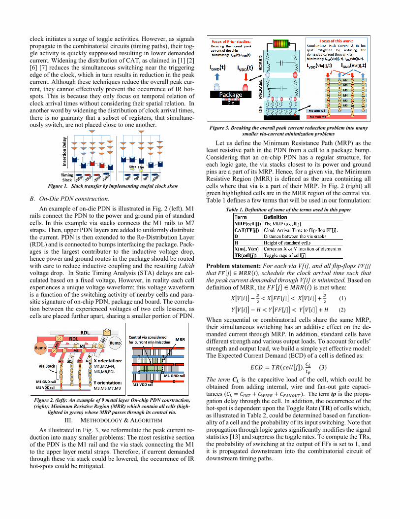
ent sources of on chip variability should be modeled and mar-gined for. One of the sources of on-chip variability is dynamic IR drop and its implied cycle to cycle voltage variation. The ex-cessive IR drop or large cycle to cycle voltage variation could cause various forms of timing failure. Considering that timing failure of a single timing path is enough to make a chip non-functional, the margins for IR drop and voltage noise, are calcu-lated based on the worst-case scenarios. The impact of IR drop, and voltage variation worsens at scaled voltages; with 5% volt-age noise in a design that operates at Super Threshold Voltage (STV) 10-20% performance variation is expected [9]. However, at Near Threshold Voltage (NTV), 5% voltage noise may cause more than ~200% performance variation [9]. To guard the de-sign against timing failures, during physical design and timing closure, large design margins for IR-drop and endpoint uncer-tainty are adopted, paying the price in terms of performance, power and area penalties. A. Useful skew for IR drop reduction
The conventional goal of CTS algorithms was to build a clock tree with zero skew to distribute the timing slacks evenly between various pipeline stages. More advanced CTS flows ex-plored the concept of useful skew to transfer slacks from shorter pipeline stages to longer ones [10]. Engineering useful skews, as illustrated in example in Fig. 1, is now widely adopted in many commercial EDAs [11] [12] to ease the timing closure and for gaining Power, Performance and Area (PPA) benefits. Timing slacks could be moved across many stages until delivered to the target stage. In addition to timing closure, the useful skew is lev-eraged for reduction of peak current. Each triggering edge of the
clock initiates a surge of toggle activities. However, as signals propagate in the combinatorial circuits (timing paths), their tog-gle activity is quickly suppressed resulting in lower demanded current. Widening the distribution of CAT, as claimed in [1] [2] [6] [7] reduces the simultaneous switching near the triggering edge of the clock, which in turn results in reduction in the peak current. Although these techniques reduce the overall peak cur-rent, they cannot effectively prevent the occurrence of IR hot-spots. This is because they only focus on temporal relation of clock arrival times without considering their spatial relation. In another word by widening the distribution of clock arrival times, there is no guaranty that a subset of registers, that simultane-ously switch, are not placed close to one another.
B. On-Die PDN construction. An example of on-die PDN is illustrated in Fig. 2 (left). M1
rails connect the PDN to the power and ground pin of standard cells. In this example via stacks connects the M1 rails to M7 straps. Then, upper PDN layers are added to uniformly distribute the current. PDN is then extended to the Re-Distribution Layer (RDL) and is connected to bumps interfacing the package. Pack-ages is the largest contributor to the inductive voltage drop, hence power and ground routes in the package should be routed with care to reduce inductive coupling and the resulting Ldi/dt voltage drop. In Static Timing Analysis (STA) delays are cal-culated based on a fixed voltage, However, in reality each cell experiences a unique voltage waveform; this voltage waveform is a function of the switching activity of nearby cells and para-sitic signature of on-chip PDN, package and board. The correla-tion between the experienced voltages of two cells lessens, as cells are placed further apart, sharing a smaller portion of PDN.
Figure 2. (left): An example of 9 metal layer On-chip PDN construction, (right): Minimum Resistive Region (MRR) which contain all cells (high-
lighted in green) whose MRP passes through its central via. III. METHODOLOGY & ALGORITHM
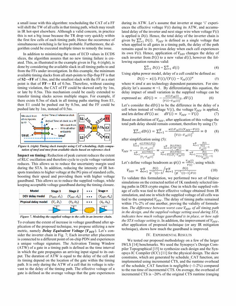
As illustrated in Fig. 3, we reformulate the peak current re-duction into many smaller problems: The most resistive section of the PDN is the M1 rail and the via stack connecting the M1 to the upper layer metal straps. Therefore, if current demanded through these via stack could be lowered, the occurrence of IR hot-spots could be mitigated.
Figure 3. Breaking the overall peak current reduction problem into many
smaller via-current minimization problems
Let us define the Minimum Resistance Path (MRP) as the least resistive path in the PDN from a cell to a package bump. Considering that an on-chip PDN has a regular structure, for each logic gate, the via stacks closest to its power and ground pins are a part of its MRP. Hence, for a given via, the Minimum Resistive Region (MRR) is defined as the area containing all cells where that via is a part of their MRP. In Fig. 2 (right) all green highlighted cells are in the MRR region of the central via. Table 1 defines a few terms that will be used in our formulation:
Table 1. Definition of some of the terms used in this paper
Problem statement: For each via V[i], and all flip-flops FF[j] that 𝐹𝐹 𝑗 ∈ 𝑀𝑅𝑅 𝑖 , schedule the clock arrival time such that the peak current demanded through V[i] is minimized. Based on definition of MRR, the 𝐹𝐹 𝑗 ∈ 𝑀𝑅𝑅 𝑖 is met when:
𝑋 𝑉 𝑖 − *+< 𝑋 𝐹𝐹 𝑗 < 𝑋 𝑉 𝑖 + *
+ (1)
𝑌 𝑉 𝑖 − 𝐻 < 𝑌 𝐹𝐹 𝑗 < 𝑌 𝑉 𝑖 + 𝐻 (2)
When sequential or combinatorial cells share the same MRP, their simultaneous switching has an additive effect on the de-manded current through MRP. In addition, standard cells have different strength and various output loads. To account for cells’ strength and output load, we build a simple yet effective model: The Expected Current Demand (ECD) of a cell is defined as:
𝐸𝐶𝐷 = 𝑇𝑅 𝑐𝑒𝑙𝑙 𝑗 . :;<=
(3)
The term CL is the capacitive load of the cell, which could be obtained from adding internal, wire and fan-out gate capaci-tances (𝐶> = 𝐶?@A + 𝐶B?CD + 𝐶EF@GHA). The term tp is the propa-gation delay through the cell. In addition, the occurrence of the hot-spot is dependent upon the Toggle Rate (TR) of cells which, as illustrated in Table 2, could be determined based on function-ality of a cell and the probability of its input switching. Note that propagation through logic gates significantly modifies the signal statistics [13] and suppress the toggle rates. To compute the TRs, the probability of switching at the output of FFs is set to 1, and it is propagated downstream into the combinatorial circuit of downstream timing paths.
Figure 1. Slack transfer by implementing useful clock skew
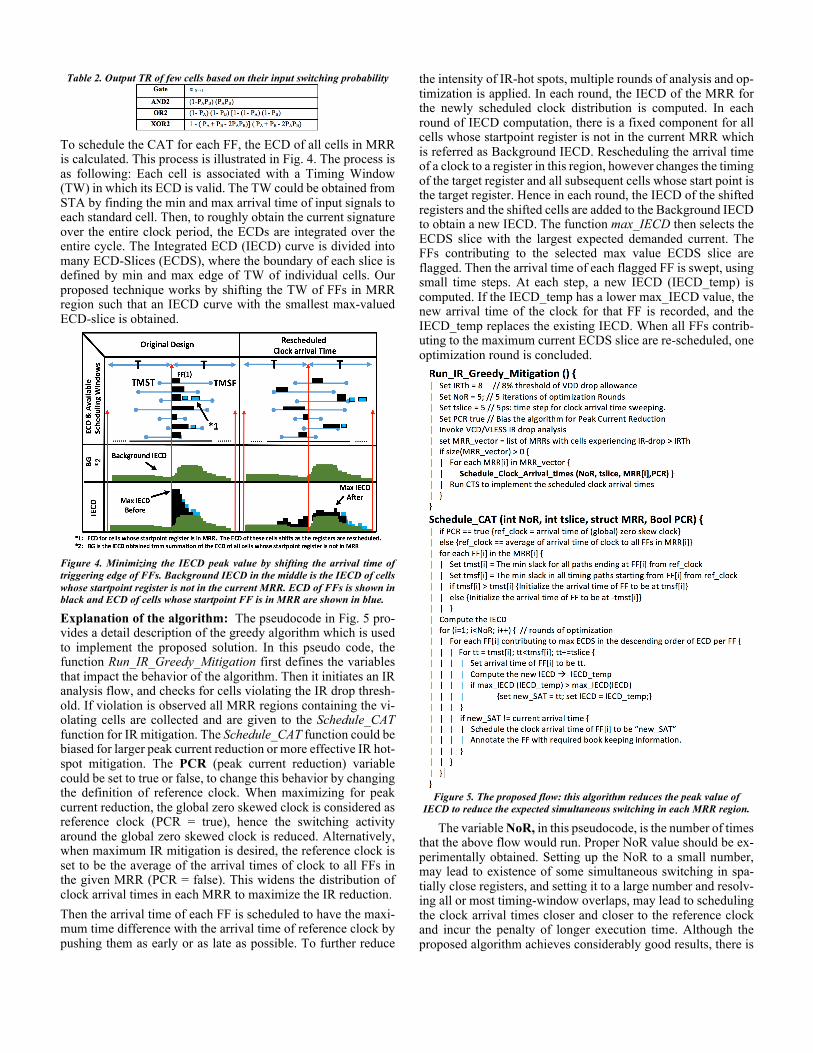
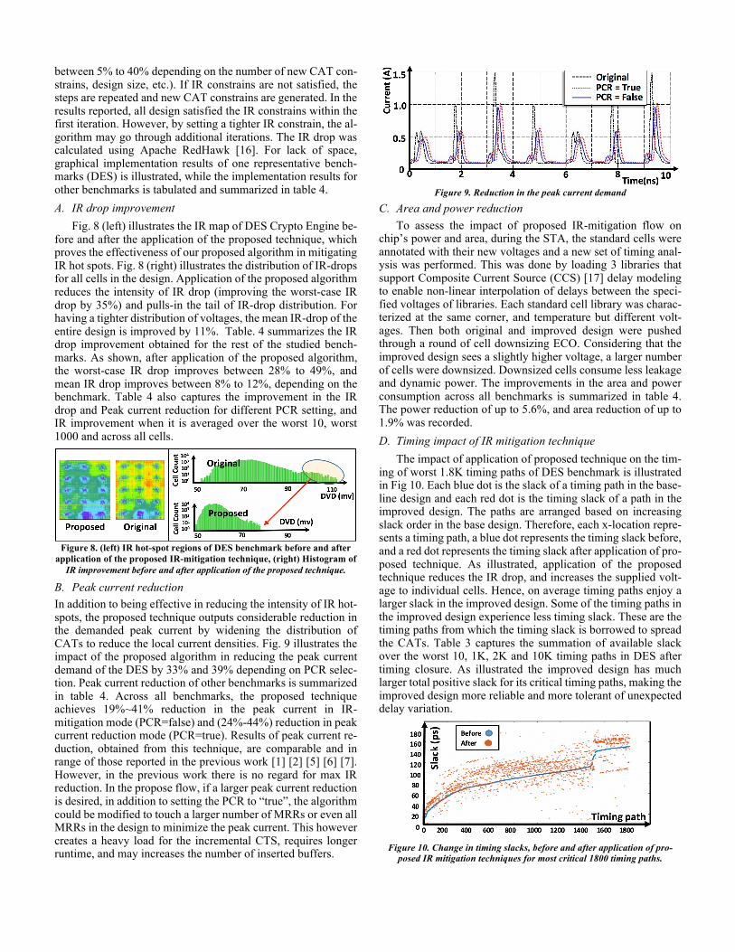
Table 2. Output TR of few cells based on their input switching probability
To schedule the CAT for each FF, the ECD of all cells in MRR is calculated. This process is illustrated in Fig. 4. The process is as following: Each cell is associated with a Timing Window (TW) in which its ECD is valid. The TW could be obtained from STA by finding the min and max arrival time of input signals to each standard cell. Then, to roughly obtain the current signature over the entire clock period, the ECDs are integrated over the entire cycle. The Integrated ECD (IECD) curve is divided into many ECD-Slices (ECDS), where the boundary of each slice is defined by min and max edge of TW of individual cells. Our proposed technique works by shifting the TW of FFs in MRR region such that an IECD curve with the smallest max-valued ECD-slice is obtained.
Figure 4. Minimizing the IECD peak value by shifting the arrival time of triggering edge of FFs. Background IECD in the middle is the IECD of cells whose startpoint register is not in the current MRR. ECD of FFs is shown in black and ECD of cells whose startpoint FF is in MRR are shown in blue.
Explanation of the algorithm: The pseudocode in Fig. 5 pro-vides a detail description of the greedy algorithm which is used to implement the proposed solution. In this pseudo code, the function Run_IR_Greedy_Mitigation first defines the variables that impact the behavior of the algorithm. Then it initiates an IR analysis flow, and checks for cells violating the IR drop thresh-old. If violation is observed all MRR regions containing the vi-olating cells are collected and are given to the Schedule_CAT function for IR mitigation. The Schedule_CAT function could be biased for larger peak current reduction or more effective IR hot-spot mitigation. The PCR (peak current reduction) variable could be set to true or false, to change this behavior by changing the definition of reference clock. When maximizing for peak current reduction, the global zero skewed clock is considered as reference clock (PCR = true), hence the switching activity around the global zero skewed clock is reduced. Alternatively, when maximum IR mitigation is desired, the reference clock is set to be the average of the arrival times of clock to all FFs in the given MRR (PCR = false). This widens the distribution of clock arrival times in each MRR to maximize the IR reduction. Then the arrival time of each FF is scheduled to have the maxi-mum time difference with the arrival time of reference clock by pushing them as early or as late as possible. To further reduce
the intensity of IR-hot spots, multiple rounds of analysis and op-timization is applied. In each round, the IECD of the MRR for the newly scheduled clock distribution is computed. In each round of IECD computation, there is a fixed component for all cells whose startpoint register is not in the current MRR which is referred as Background IECD. Rescheduling the arrival time of a clock to a register in this region, however changes the timing of the target register and all subsequent cells whose start point is the target register. Hence in each round, the IECD of the shifted registers and the shifted cells are added to the Background IECD to obtain a new IECD. The function max_IECD then selects the ECDS slice with the largest expected demanded current. The FFs contributing to the selected max value ECDS slice are flagged. Then the arrival time of each flagged FF is swept, using small time steps. At each step, a new IECD (IECD_temp) is computed. If the IECD_temp has a lower max_IECD value, the new arrival time of the clock for that FF is recorded, and the IECD_temp replaces the existing IECD. When all FFs contrib-uting to the maximum current ECDS slice are re-scheduled, one optimization round is concluded.
Figure 5. The proposed flow: this algorithm reduces the peak value of
IECD to reduce the expected simultaneous switching in each MRR region.
The variable NoR, in this pseudocode, is the number of times that the above flow would run. Proper NoR value should be ex-perimentally obtained. Setting up the NoR to a small number, may lead to existence of some simultaneous switching in spa-tially close registers, and setting it to a large number and resolv-ing all or most timing-window overlaps, may lead to scheduling the clock arrival times closer and closer to the reference clock and incur the penalty of longer execution time. Although the proposed algorithm achieves considerably good results, there is
a small issue with this algorithm: rescheduling the CAT of a FF will shift the TW of all cells in that timing path, which may result in IR hot-spot elsewhere. Although a valid concern, in practice this is not a big issue because the TR drop very quickly within the first few cells of each timing path; Hence the occurrence of simultaneous switching is far less probable. Furthermore, the al-gorithm could be executed multiple times to remedy the issue.
In addition to minimizing the sum of ECD values in ECDS slices, the algorithm assures that no new timing failure is cre-ated. This, as illustrated in the example given in Fig. 6 (right), is done by considering the available slack in all timing paths to and from the FFs under investigation. In this example, the minimum available timing slacks from all start-points to flip-flop FF is that of S2→FF of 1.0ns, and the smallest slack with the FF as a start point is that of FF→ E1 of 0.5ns. Therefore, without causing timing violation, the CAT of FF could be skewed early by 1ns, or late by 0.5ns. This mechanism could be easily extended to transfer timing slacks across multiple stages. For example, if there exists 0.5ns of slack in all timing paths starting from E1, then E1 could be pushed out by 0.5ns, and the FF could be pushed late by 1ns, instead of 0.5ns.
Figure 6. (right) Timing slack transfer using CAT scheduling, (left) compu-
tation of tmsf and tmst from available slacks based on reference clock
Impact on timing: Reduction of peak current reduces the extent of RLC oscillation and therefore cycle to cycle voltage variation reduces. This allows us to reduce the uncertainty margin used during the STA. In addition, reducing the intensity of IR hot-spots translates to higher voltage at the PG pins of standard cells, boosting their speed and providing them with higher voltage gaurdband. This allows us to reduce the supplied voltage, while keeping acceptable voltage gaurdband during the timing closure.
Figure 7. Modeling the supplied voltage to the cells in an inverter chain.
To evaluate the extent of increase in voltage gaurdband after ap-plication of the proposed technique, we propose utilizing a new metric, namely Delay Equivalent Voltage (𝑽𝑫𝑬𝑽). Let’s con-sider the inverter chain in Fig. 7; Each inverter after placement is connected to a different point of on-chip PDN and experiences a unique voltage signature. The Activation Timing Window (ATW) of a gate in a timing path is defined as the time interval in which the gate propagates an arriving input signal to its out-put. The duration of ATW is equal to the delay of the cell and its timing depend on the location of the gate within the timing path. It is only during the ATW of a cell that its voltage is rele-vant to the delay of the timing path. The effective voltage of a gate is defined as the average voltage that the gate experiences
during its ATW. Let’s assume that inverter at stage ‘i’ experi-ences the effective voltage 𝑉(𝑖) during its ATW, and accumu-lated delay of the inverter and next stage wire when voltage 𝑉(𝑖) is applied is 𝐷(𝑖). Hence, the total delay of the inverter chain is given by 𝐷(𝑖)@
NOP . 𝑉*DQ is defined as a single voltage that when applied to all gates in a timing path, the delay of the path remains equal to its previous delay when each cell experiences its own 𝑉(𝑖). Hence, application of 𝑉*DQchanges the delay of each inverter from 𝐷 𝑖 to a new value 𝑑 𝑖 , however the fol-lowing equation remains valid:
𝐷(𝑖)@NOP = 𝑑(𝑖)@
NOP (4) Using alpha power model, delay of a cell could be defined as:
𝐷(𝑖)~𝜅(𝑖). 𝑉(𝑖) 𝑉(𝑖) − 𝑉<V(𝑖) ∝ (5) where ∝ 𝑎𝑛𝑑𝜅 are technology dependent parameters. For sim-plicity let’s assume ∝ =1. By differentiating this equation, the delay impact of small variation in the supplied voltage can be expressed as: 𝑑𝐷(𝑖) = − Z(N).Q[\ N
Q N ]Q[\ N ^ . 𝑑𝑉(𝑖) (6)
Let’s consider the 𝑑𝐷(𝑖) to be the difference in the delay of a cell when instead of voltage V(𝑖), the voltage 𝑉*DQ is applied, and lets define 𝑑𝑉 𝑖 as: 𝑑𝑉 𝑖 = 𝑉*DQ − 𝑉 𝑖 (7) Based on definition of 𝑉*DQ, after application of this voltage the total path delay should remain constant, therefore by using (7):
𝑑𝐷 𝑖 =@NOP − 𝜅 𝑖 .𝑉𝑡ℎ 𝑖 .(𝑉𝐷𝐸𝑉−𝑉 𝑖 )
𝑉 𝑖 −𝑉𝑡ℎ 𝑖2
𝑁𝑖=1 = 0 (8)
after simplification using (5):
𝑉*DQ =
𝜅 𝑖 𝑉𝑡ℎ 𝑖 .𝑉(𝑖)
𝑉𝑖−𝑉𝑡ℎ 𝑖2
𝑁𝑖=1
𝜅 𝑖 𝑉𝑡ℎ 𝑖
𝑉𝑖−𝑉𝑡ℎ 𝑖2
𝑁𝑖=1
=𝐷 𝑖 .𝑉𝑡ℎ 𝑖𝑉𝑖−𝑉𝑡ℎ 𝑖
𝑁𝑖=1
𝐷 𝑖 .𝑉𝑡ℎ 𝑖𝑉 𝑖 .(𝑉𝑖−𝑉𝑡ℎ 𝑖 )
𝑁𝑖=1
=
𝐷 𝑖𝑉(𝑖)𝑉𝑡ℎ(𝑖)
−1𝑁𝑖=1
𝐷 𝑖𝑉 𝑖 .( 𝑉(𝑖)𝑉𝑡ℎ(𝑖)
−1)𝑁𝑖=1
(9)
Let’s define voltage headroom as 𝜓 𝑖 = Q[\ NQ N
, using which:
𝑉*DQ = 𝐷(𝑖)
𝜓−1(𝑖)−1𝑁𝑖=1
𝐷(𝑖)𝜓−1(𝑖)−1 .𝑉 𝑖
𝑁𝑖=1 (10)
To validate this formulation, we performed two set of Hspice simulations on the extracted netlist of 1K randomly selected tim-ing paths in DES crypto engine. One in which the supplied volt-age of cells was tied to their effective voltage obtained from IR simulation, and one in which the supplied voltage of all cells was tied to the computed 𝑉*DQ. The delay of timing paths remained within 1%-2% of one another, proving the validity of formula-tion. The difference between worst case 𝑉*DQ of all timing path in the design, and the supplied voltage setting used during STA, indicates how much voltage gaurdband is in place, or how safe the STA voltage setting is. In addition, the improvement of 𝑉*DQ, after application of proposed technique (or any IR mitigation technique), shows how much the gaurdband is improved.
IV. EXPERIMENTAL RESULTS We tested our proposed methodology on a few of the larger
IWLS [14] benchmarks. We used the Synopsys’s Design Com-piler Topographical [15] to synthesize each design and the Syn-opsys IC Compiler (ICC) [11] for the physical design. The skew constrains, which are generated by schedule_CAT function, are implemented using incremental CTS, and the runtime overhead of the schedule_CAT function is negligible (~1-2%) compared to the run time of incremental CTS. On average, the overhead of incremental CTS is ~20% of the original CTS runtime (ranging
between 5% to 40% depending on the number of new CAT con-strains, design size, etc.). If IR constrains are not satisfied, the steps are repeated and new CAT constrains are generated. In the results reported, all design satisfied the IR constrains within the first iteration. However, by setting a tighter IR constrain, the al-gorithm may go through additional iterations. The IR drop was calculated using Apache RedHawk [16]. For lack of space, graphical implementation results of one representative bench-marks (DES) is illustrated, while the implementation results for other benchmarks is tabulated and summarized in table 4. A. IR drop improvement
Fig. 8 (left) illustrates the IR map of DES Crypto Engine be-fore and after the application of the proposed technique, which proves the effectiveness of our proposed algorithm in mitigating IR hot spots. Fig. 8 (right) illustrates the distribution of IR-drops for all cells in the design. Application of the proposed algorithm reduces the intensity of IR drop (improving the worst-case IR drop by 35%) and pulls-in the tail of IR-drop distribution. For having a tighter distribution of voltages, the mean IR-drop of the entire design is improved by 11%. Table. 4 summarizes the IR drop improvement obtained for the rest of the studied bench-marks. As shown, after application of the proposed algorithm, the worst-case IR drop improves between 28% to 49%, and mean IR drop improves between 8% to 12%, depending on the benchmark. Table 4 also captures the improvement in the IR drop and Peak current reduction for different PCR setting, and IR improvement when it is averaged over the worst 10, worst 1000 and across all cells.
Figure 8. (left) IR hot-spot regions of DES benchmark before and after
application of the proposed IR-mitigation technique, (right) Histogram of IR improvement before and after application of the proposed technique.
B. Peak current reduction In addition to being effective in reducing the intensity of IR hot-spots, the proposed technique outputs considerable reduction in the demanded peak current by widening the distribution of CATs to reduce the local current densities. Fig. 9 illustrates the impact of the proposed algorithm in reducing the peak current demand of the DES by 33% and 39% depending on PCR selec-tion. Peak current reduction of other benchmarks is summarized in table 4. Across all benchmarks, the proposed technique achieves 19%~41% reduction in the peak current in IR-mitigation mode (PCR=false) and (24%-44%) reduction in peak current reduction mode (PCR=true). Results of peak current re-duction, obtained from this technique, are comparable and in range of those reported in the previous work [1] [2] [5] [6] [7]. However, in the previous work there is no regard for max IR reduction. In the propose flow, if a larger peak current reduction is desired, in addition to setting the PCR to “true”, the algorithm could be modified to touch a larger number of MRRs or even all MRRs in the design to minimize the peak current. This however creates a heavy load for the incremental CTS, requires longer runtime, and may increases the number of inserted buffers.
Figure 9. Reduction in the peak current demand
C. Area and power reduction To assess the impact of proposed IR-mitigation flow on
chip’s power and area, during the STA, the standard cells were annotated with their new voltages and a new set of timing anal-ysis was performed. This was done by loading 3 libraries that support Composite Current Source (CCS) [17] delay modeling to enable non-linear interpolation of delays between the speci-fied voltages of libraries. Each standard cell library was charac-terized at the same corner, and temperature but different volt-ages. Then both original and improved design were pushed through a round of cell downsizing ECO. Considering that the improved design sees a slightly higher voltage, a larger number of cells were downsized. Downsized cells consume less leakage and dynamic power. The improvements in the area and power consumption across all benchmarks is summarized in table 4. The power reduction of up to 5.6%, and area reduction of up to 1.9% was recorded. D. Timing impact of IR mitigation technique
The impact of application of proposed technique on the tim-ing of worst 1.8K timing paths of DES benchmark is illustrated in Fig 10. Each blue dot is the slack of a timing path in the base-line design and each red dot is the timing slack of a path in the improved design. The paths are arranged based on increasing slack order in the base design. Therefore, each x-location repre-sents a timing path, a blue dot represents the timing slack before, and a red dot represents the timing slack after application of pro-posed technique. As illustrated, application of the proposed technique reduces the IR drop, and increases the supplied volt-age to individual cells. Hence, on average timing paths enjoy a larger slack in the improved design. Some of the timing paths in the improved design experience less timing slack. These are the timing paths from which the timing slack is borrowed to spread the CATs. Table 3 captures the summation of available slack over the worst 10, 1K, 2K and 10K timing paths in DES after timing closure. As illustrated the improved design has much larger total positive slack for its critical timing paths, making the improved design more reliable and more tolerant of unexpected delay variation.
Figure 10. Change in timing slacks, before and after application of pro-
posed IR mitigation techniques for most critical 1800 timing paths.
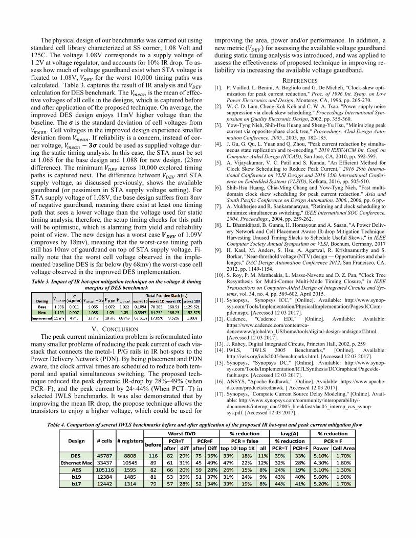
The physical design of our benchmarks was carried out using standard cell library characterized at SS corner, 1.08 Volt and 125C. The voltage 1.08V corresponds to a supply voltage of 1.2V at voltage regulator, and accounts for 10% IR drop. To as-sess how much of voltage gaurdband exist when STA voltage is fixated to 1.08V, 𝑉*DQ for the worst 10,000 timing paths was calculated. Table 3. captures the result of IR analysis and 𝑉*DQ calculation for DES benchmark. The 𝑉fghiis the mean of effec-tive voltages of all cells in the designs, which is captured before and after application of the proposed technique. On average, the improved DES design enjoys 11mV higher voltage than the baseline. The 𝝈 is the standard deviation of cell voltages from 𝑉fghi. Cell voltages in the improved design experience smaller deviation from 𝑉fghi. If reliability is a concern, instead of cor-ner voltage, 𝑉fghi − 𝟑𝝈 could be used as supplied voltage dur-ing the static timing analysis. In this case, the STA must be set at 1.065 for the base design and 1.088 for new design. (23mv difference). The minimum 𝑉*DQ across 10,000 explored timing paths is captured next. The difference between 𝑉*DQ and STA supply voltage, as discussed previously, shows the available gaurdband (or pessimism in STA supply voltage setting). For STA supply voltage of 1.08V, the base design suffers from 8mv of negative gaurdband, meaning there exist at least one timing path that sees a lower voltage than the voltage used for static timing analysis; therefore, the setup timing checks for this path will be optimistic, which is alarming from yield and reliability point of view. The new design has a worst case 𝑽𝑫𝑬𝑽 of 1.09V (improves by 18mv), meaning that the worst-case timing path still has 10mv of gaurdband on top of STA supply voltage. Fi-nally note that the worst cell voltage observed in the imple-mented baseline DES is far below (by 68mv) the worst-case cell voltage observed in the improved DES implementation. Table 3. Impact of IR hot-spot mitigation technique on the voltage & timing
margins of DES benchmark
V. CONCLUSION
The peak current minimization problem is reformulated into many smaller problems of reducing the peak current of each via-stack that connects the metal-1 P/G rails in IR hot-spots to the Power Delivery Network (PDN). By being placement and PDN aware, the clock arrival times are scheduled to reduce both tem-poral and spatial simultaneous switching. The proposed tech-nique reduced the peak dynamic IR-drop by 28%~49% (when PCR=F), and the peak current by 24~44% (When PCT=T) in selected IWLS benchmarks. It was also demonstrated that by improving the mean IR drop, the propose technique allows the transistors to enjoy a higher voltage, which could be used for
improving the area, power and/or performance. In addition, a new metric (𝑉*DQ)for assessing the available voltage gaurdband during static timing analysis was introduced, and was applied to assess the effectiveness of proposed technique in improving re-liability via increasing the available voltage gaurdband.
REFERENCES [1]. P. Vuillod, L. Benini, A. Bogliolo and G. De Micheli, "Clock-skew opti-
mization for peak current reduction," Proc. of 1996 Int. Symp. on Low Power Electronics and Design, Monterey, CA, 1996, pp. 265-270.
[2]. W. C. D. Lam, Cheng-Kok Koh and C. W. A. Tsao, "Power supply noise suppression via clock skew scheduling," Proceedings International Sym-posium on Quality Electronic Design, 2002, pp. 355-360.
[3]. Yow-Tyng Nieh, Shih-Hsu Huang and Sheng-Yu Hsu, "Minimizing peak current via opposite-phase clock tree," Proceedings. 42nd Design Auto-mation Conference, 2005., 2005, pp. 182-185.
[4]. J. Gu, G. Qu, L. Yuan and Q. Zhou, "Peak current reduction by simulta-neous state replication and re-encoding," 2010 IEEE/ACM Int. Conf. on Computer-Aided Design (ICCAD), San Jose, CA, 2010, pp. 592-595.
[5]. A. Vijayakumar, V. C. Patil and S. Kundu, "An Efficient Method for Clock Skew Scheduling to Reduce Peak Current," 2016 29th Interna-tional Conference on VLSI Design and 2016 15th International Confer-ence on Embedded Systems (VLSID), Kolkata, 2016, pp. 505-510.
[6]. Shih-Hsu Huang, Chia-Ming Chang and Yow-Tyng Nieh, "Fast multi-domain clock skew scheduling for peak current reduction," Asia and South Pacific Conference on Design Automation, 2006., 2006, pp. 6 pp.-
[7]. A. Mukherjee and R. Sankaranarayan, "Retiming and clock scheduling to minimize simultaneous switching," IEEE International SOC Conference, 2004. Proceedings., 2004, pp. 259-262.
[8]. L. Bhamidipati, B. Gunna, H. Homayoun and A. Sasan, "A Power Deliv-ery Network and Cell Placement Aware IR-drop Mitigation Technique: Harvesting Unused Timing Slacks to Schedule Useful Skews," in IEEE Computer Society Annual Symposium on VLSI, Bochum, Germany, 2017
[9]. H. Kaul, M. Anders, S. Hsu, A. Agarwal, R. Krishnamurthy and S. Borkar, "Near-threshold voltage (NTV) design — Opportunities and chal-lenges," DAC Design Automation Conference 2012, San Francisco, CA, 2012, pp. 1149-1154.
[10]. S. Roy, P. M. Mattheakis, L. Masse-Navette and D. Z. Pan, "Clock Tree Resynthesis for Multi-Corner Multi-Mode Timing Closure," in IEEE Transactions on Computer-Aided Design of Integrated Circuits and Sys-tems, vol. 34, no. 4, pp. 589-602, April 2015.
[11]. Synopsys, "Synopsys ICC," [Online]. Available: http://www.synop-sys.com/Tools/Implementation/PhysicalImplementation/Pages/ICCom-piler.aspx. [Accessed 12 03 2017].
[12]. Cadence, "Cadence EDI," [Online]. Available: Available: https://www.cadence.com/content/ca-dencewww/global/en_US/home/tools/digital-design-andsignoff.html. [Accessed 12 03 2017].
[13]. J. Rabey, Digital Integrated Circuts, Princton Hall, 2002, p. 259 [14]. IWLS, "IWLS 2005 Benchmarks," [Online]. Available:
http://iwls.org/iwls2005/benchmarks.html. [Accessed 12 03 2017]. [15]. Synopsys, "Synopsys DC," [Online]. Available: http://www.synop-
sys.com/Tools/Implementation/RTLSynthesis/DCGraphical/Pages/de-fault.aspx. [Accessed 12 03 2017].
[16]. ANSYS, "Apache Redhawk," [Online]. Available: https://www.apache-da.com/products/redhawk. [ Accessed 12 03 2017]
[17]. Synopsys, "Compsite Current Source Delay Modeling," [Online]. Avail-able: http://www.synopsys.com/community/interoperability/- documents/interop_dac/2005_breakfast/dac05_interop_ccs_synop-sys.pdf. [Accessed 12 03 2017].
Table 4. Comparison of several IWLS benchmarks before and after application of the proposed IR hot-spot and peak current mitigation flow