Embed Size (px)
Citation preview
Draft B Page i
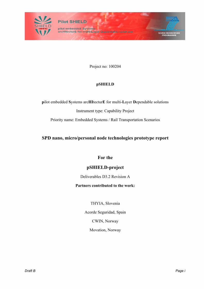
Project no: 100204
pSHIELD
pilot embedded Systems arcHItecturE for multi-Layer Dependable solutions
Instrument type: Capability Project
Priority name: Embedded Systems / Rail Transportation Scenarios
SPD nano, micro/personal node technologies prototype report
For the
pSHIELD-project
Deliverables D3.2 Revision A
Partners contributed to the work:
THYIA, Slovenia
Acorde Seguridad, Spain
CWIN, Norway
Movation, Norway

Draft B Page ii
Project co-funded by the European Commission within the Seventh Framework Programme (2007-2012) Dissemination Level PU Public X PP Restricted to other programme participants (including the Commission Services) RE Restricted to a group specified by the consortium (including the Commission Services) CO Confidential, only for members of the consortium (including the Commission Services)
Document Authors and Approvals Authors
Date Signature Name Company Spase Drakul THYIA
Ljiljana Mijic THYIA
Vlado Drakulovski THYIA
Gordana Mijic THYIA
Nastja Kuzmin THYIA
Silvia Mier ACORDE
Jaime Sanchez ACORDE
Sarfraz Alam CWIN
Josef Noll Movation
Reviewed by
Name Company
Gareth May-Clement Critical Softwaree
Approved by
Name Company
Modification History Issue Date Description Draft A 08.06.2011 First issue for comments
Issue B 30.12.2011 Incorporates comments from Draft A review
Issue 1 05.01.2012 Incorporates comments from issue 1 review

Draft B Page iii
Contents 1 Executive Summary .................................................................. 11
2 Introduction ................................................................................ 13
3 Nano, Micro/Personal SPD Node Technologies ..................... 16 3.1 Pervasive computing ...................................................................... 16 3.2 A general SPD node description ................................................... 17
3.2.1 Formal conceptual model ................................................................... 17
3.3 SPD node functionalities ............................................................... 20 3.3.1 SPD functionalities .............................................................................. 20
3.4 NMP-SPD node technologies ........................................................ 22 3.4.1 NMP-SPD nodes ................................................................................ 22 3.4.2 NMP node operating systems ............................................................. 25
4 Wireless Sensor Networks ....................................................... 27 4.1 Sensor nodes in WSNs .................................................................. 28
4.1.1 Middleware ......................................................................................... 29 4.1.2 Securing embedded systems ......................................................... 32 4.1.3 General security requirements ............................................................ 34 4.1.4 Multidimensional metric space ............................................................ 38
5 Firmware, Secure SoC, and Trust ........................................ 43 5.1 Firmware .......................................................................................... 43
5.1.1 Security requirements for ES firmware ............................................... 43 5.1.2 Secure SoC ........................................................................................ 45 5.1.3 Security in firmware updates systems ................................................ 46 5.1.4 TPM, MTM and secure boot ............................................................... 47
6 Power Supply Protections ..................................................... 54 6.1 Power Supply Source ..................................................................... 54
6.1.1 Power Supply Components ................................................................ 54 6.1.2 Conclusions ........................................................................................ 62
7 Elliptic Curve Cryptography for NMP Nodes .......................... 63 7.1 Public key infrastructure ................................................................ 63
7.1.1 ECC Applications ................................................................................ 64

Draft B Page iv
7.2 Signature schemes ......................................................................... 64 7.2.1 Proxy blind signature scheme ............................................................. 65
7.3 ECC in software trusted platform module .................................... 67 7.3.1 SW-TPM Implementation .................................................................... 68 7.3.2 Measurement results .......................................................................... 68 7.3.3 User applications with SW-TPM ......................................................... 70
7.4 Electromagnetic analysis ECC on a PDA ..................................... 71 7.4.1 Differential analysis in the frequency domain ..................................... 72
7.5 ECC in wireless sensors ................................................................ 73 7.6 Improvements in ECC for resource-constrained devices ........... 73
7.6.1 Key agreement protocol for mobile devices on elliptic curve cryptosystem ....................................................................................... 74
7.7 Comparison: ECC vs. Others Alternative Cryptography for Resource-Constrained Devices ............................................... 75
Weakness ..................................................................................................... 76
8 NMP Node: Prototypes .............................................................. 79 8.1 Adaptation of off-the-shelf sensors .............................................. 79 8.2 Development platform .................................................................... 81
8.2.1 NMPS node prototype ........................................................................ 81
9 Confidentiality, Integrity, Authenticity, Availability and System Integrity in WSNs ......................................................... 89 9.1 Security enhancements: performance evaluation ....................... 89
9.1.1 Experiments ........................................................................................ 90 9.1.2 Future work ......................................................................................... 92
10 Conclusions ............................................................................... 93
11 Appendix: STM32 chip ............................................................. 96 11.1 The Cortex™-M3 based STM32 ..................................................... 96
11.1.1 The ARM Cortex - M3 ......................................................................... 96 11.1.2 The Cortex-M3 Processor vs Cortex-M3-Based MCUs ...................... 96 11.1.3 Architecture ......................................................................................... 98 11.1.4 STM32F ............................................................................................ 100 11.1.5 STM32W ........................................................................................... 106
12 References ............................................................................... 108
Draft B Page v
Figures
Figure 3-1: Formal conceptual model of a pSHIELD Node. ....................................................................... 18
Figure 3-2: pSHIELD functional component architecture. ......................................................................... 19
Figure 3-3: SPD node concept as in D3.3. ................................................................................................. 19
Figure 3-4: Hardware architecture and nano node chip partitioning. .......................................................... 24
Figure 4-1: WSN composed of NMP and power nodes. ............................................................................. 27
Figure 4-2: A reference model for middleware in WSNs. ........................................................................... 30
Figure 4-3: The Hydra middleware layer. ................................................................................................... 32
Figure 4-4: Embedded security pyramid. .................................................................................................... 33
Figure 4-5: SW update model for WSNs. ................................................................................................... 37
Figure 5-1: A schematic view on a secure Soc architecture. ...................................................................... 45
Figure 5-2: An exemplary flow for a firmware update process using the microprogrammer approach. ..... 47
Figure 5-3: An exemplary flow for a firmware update process using the boot loader approach. ................ 47
Figure 5-4: Elements of the secure boot pattern. ....................................................................................... 49
Figure 5-5: ARM TrustZone SW architecture. ............................................................................................ 50
Figure 5-6: Security architecture for sensor node using Arm11 with Trust zone features. ......................... 51
Figure 6-1: Protection circuit board – Nano and micro nodes. ................................................................... 60
Figure 6-2: DC Protection board – power control and monitoring. ............................................................. 61
Figure 6-3: DC Protection board. ................................................................................................................ 62
Figure 8-1: Nano, Micro/Personal nodes used for KBV prototype. ............................................................. 80
Figure 8-2: Comparison of sensor node platforms. .................................................................................... 83
Figure 8-3: NMPS node prototype architecture. ......................................................................................... 85
Figure 8-4: A demo development prototype board. .................................................................................... 85
Figure 8-5: Block diagram of Amtel AT97SC3203S TPM. .......................................................................... 87
Figure 8-6: TPM Amtel AT97SC3203S unit. ............................................................................................... 87

Draft B Page vi
Figure 9-1: Symmetric session key request operation with trusted NMPS nodes: a) between Node A and GW, b) between Nodes A, B and C grace a secession key Kabc generated by GW on the request from Node A......................................................................................................................................... 91
Figure 11-1: STM32 Cortex - M3 implementation ....................................................................................... 97
Figure 11-2: Cortex - M3 ............................................................................................................................ 98
Figure 11-3: Performance Line Pinout. ..................................................................................................... 101
Figure 11-4: Performance Line Block Diagram ......................................................................................... 102
Figure 11-5: System Architecture ............................................................................................................. 102
Figure 11-6: STM32F103 Memory Map .................................................................................................... 104
Tables Table 3-1: An example of NMP-SPD components. ................................................................................... 23
Table 4-1: Typical threats in WSNs. ........................................................................................................... 36
Table 5-1: Comparison study on trusted implementation for WSNs. .......................................................... 52
Table 6-1: Power consumption of possible models of nano nodes ............................................................ 54
Table 6-2: Power consumption of possible models of micro nodes. ........................................................... 54
Table 6-3: Batteries - specifications ............................................................................................................ 55
Table 6-4: Fuel cells - specifications ........................................................................................................... 56
Table 6-5: Ultracapacitors - specifications .................................................................................................. 57
Table 6-6: Power Source – solar energy. ................................................................................................... 58
Table 6-7: Power source – vibrations. ........................................................................................................ 59
Table 6-8: Power source – wind power. ..................................................................................................... 59
Table 7-1: Energy and execution time for TPM commands ........................................................................ 70
Table 7-2: Energy macromodels for the TPM_Sign and TPM_Seal. .......................................................... 70
Table 7-3: Energy and execution time for trusted applications ................................................................... 71
Table 8-1: MCU comparison. ...................................................................................................................... 82
Table 8-2: IEEE 802.15.4 chips comparison .............................................................................................. 83
Draft B Page vii
Glossary
AES Advanced Encryption Standard ADC Analog Digital Converter AOP Agent-Oriented Architecture AP Application Processor ASIC Application Specific Integrated Circuit BAN Body Area Network CCM Counter with CBC-MAC CI Critical Infrastructure CIA Confidentiality Integrity Authenticity CIAA Confidentiality Integrity Authenticity Availability CIF Common Intermediate Format COE Cryptography Operation Engine CPU Central Processing Unit DAC Digital Analog Converter DES Data Encryption Standard DH Diffie-Hellman DLP Discrete Logarithm Problem DMA Direct Memory Access DRAM Dynamic Random Access Memory DRM Digital Rights Managements DSA Digital Signature Algorithm E2E End-to-End EC Elliptic Curve ECC Elliptic Curve Cryptography ED Embedded Device ECDH Elliptic Curve Diffie Hellman ECDLP Elliptic Curve Discrete Logarithm Problem ECDSA Elliptic Curve Digital Signature Algorithm ECMQV Elliptic Curve Menezes–Qu–Vanstone EEPROM Electrically Erasable Programmable Read-Only Memory EF Elliptic Field EM Electromagnetic ES Embedded System ESD Embedded System Device FFT Fast Fourier Transform FLASH Non-Volatile Computer Storage Chip GW Gateway HbyH Hop-by-Hop HMAC Hash-based Message Authentication Code HW Hardware

Draft B Page viii
FIPS Federal Information Processing Standards FPGA Field Programmable Gate Array GCM Galois/Counter Mode GF Galois Field GPS General Purpose Processor HECC Hyper-ECC HHN Hybrid Heterogeneous Network HSM Health Status Monitoring IFP Integer Factorization Problem I/O Input/Output ITH Internet of Things and Human IoT Internet of Things IP Internet Protocol KMOV Koyama, Maurer, Okamoto & Vanstone LS-WSNs Large Scale-Wireless Sensor Networks MAC Medium Access Control MCU Microcontroller MEM Volatile Memory MEMS Micro Electromechanical Systems MIPS Million Instruction Per Second MMS Multi-dimensional Metric Space MNT Microsystems and Nano Technology MTM Mobile Trust Module MQV Menezes–Qu–Vanstone NIST National Institute of Standards and Technology NMP Nano Micro/Personal NMPS Nano Micro/Personal Sensor NSA National Security Agency NVM Non-Volatile Memory OS Operating System OSGi Open Service Gateway Initiative P2P Peer to Peer PC Pervasive Computing or Personal Computer PCR Platform Configuration Register PHY Physical PDA Personal Digital Assistant PKC Public Key Cryptography PKI Public Key Infrastructure PM Power Management PROM Programmable Read-Only Memory pSNA pSHIELD Node Adapter pSRSA pSHIELD Reference System Architecture QoS Quality of Service RAM Random Access Memory RFID Radio Frequency Identification

Draft B Page ix
RNG Random Number Generator ROM Read Only Memory RRC Reconfiguration/Recovery Controller RSA Rivest Shamir & Adleman RT Rail Transportation RTCI Rail Transportation Critical Infrastructure RWDT Recovery Watchdog Timer SCC Sensing Computation Communication SHA Secure Hash Algorithm SHSM System Health Status Monitoring SOA Service Oriented Architecture SoC System on Chip SP Security Privacy SPD Security Privacy Dependability SPI Serial Periphheral Bus SPP Special Purpose Processor SRAM Static Random Access Memory SS Stable Storage SW Software TCG Trust Computing Group TPM Trust Platform Module TZASC Trust Zone Address Space TZMA Trust Zone Memory Adapter UART Universal Asynchronous Receiver/Transmitter UCS Use Case Scenario UC Ubiquitous Computing UPC Ubiquitous and Pervasive Computing UWB Ultra Wideband VHDL Very high speed integrated circuit Hardware Description Language VoIP Voice over IP VPN Virtual Private Network WSN Wireless Sensor Network

Draft B Page x

p-SHIELD SPD nano, micro/personal node technologies prototype report
PU
PU D3.2
Draft B Page 11 of 109
1 Executive Summary This document addresses SPD (Security Privacy Dependability) nano, micro/personal (NMP) node technologies prototype. The main focus is on SPD functionalities for energy-constrained small Embedded Devices (EDs) in terms of hardware (HW) and software (SW). Wireless Sensor Networks (WSNs) that use NMP sensor (NMPS) nodes they have low processing power, limited radio ranges, very low energy consumption and perform limited functionalities. The main goals for NMP node is to provide enhancement in
- intrinsically secure ES firmware,
- secure boot,
- integrity protection of the ES firmware,
- security, privacy and dependability issues,
- secure key installation,
- secure firmware upgrade,
- power supply protection,
- protection circuits,
- remote powering and secondary power sources,
- access capabilities,
- mobility,
- sensing capabilities,
- SW upgrade for TCG (Trust Computing Group) technologies, and
- mobile trusted module (MTM).
The rail transportation (RT) systems protection is targeted application area in pSHIELD. Threats such as natural catastrophes, terroristic attacks and other kind of attacks that have been reported in recent years in this application area are demanding new SPD NMP node technologies that have SPD mechanisms as contra-measures against threats, attacks and faults. The pSHIELD concept taxonomy for SPD is addressed in D2.1.2 and D2.2.2 deliverables. There are three main groups
- threats,
- attributes and
- means,
This deliverable is focused mainly on Security and Dependability attributes, although in some cases threats and means will be also considered. Targeting the application scenario for pSHIELD project as a pilot investigation for proof-of-concepts addressed for SPD NMP technology, we are coming to the conclusion that WSNs perfectly match the needs for protecting a critical infrastructure (CI) such as the rail transportation of dangerous materials. Wireless Sensor Networks (WSNs) take today an active role for improving security, dependability, reliability, survivability and fault-tolerance, but the WSNs must be
p-SHIELD SPD nano, micro/personal node technologies prototype report
PU
PU D3.2
Draft B Page 12 of 109
improved first also to guaranty the SPD improvements. It is clear that usefulness of WSNs for RT as CI (RTCI) is primarily determined by the dependability of the WSN itself.
The NMPS node architecture is of main interest in this document, because to guaranty that a WSN with such nodes is working properly it is essential that all nodes are working properly thanks to the new SPD features considered in pSHIELD. Therefore, the approach in the pSHIELD project is to address the design problems of SPD at all layers of the architecture. Taking in consideration first unconnected NMPS nodes the primary design consideration will be on the node architecture. Connecting the NMPS nodes in a WSN the secondary design consideration will be on the layered node structure and SPD features. These two design considerations are not separable as two fully independent design constraints and therefore they require an integrative approach for NMP technology nodes based on microsystems and nano technology (MNT). Finally, the reconfigurable NMPS node can improve the processing performance of WSNs. Such reconfigurable nodes rely on the use of a microcontroller. The new design alternatives introduced with reconfigurable HW offer new advantages thanks to ASICs (Application-Specific Integrated Circuits) and GPPs (General Purpose Processors). The prototypes considered in this document are studied in all targeted SPD aspects, and the architectures for the future NMP Embedded Systems (ESs) are proposed.

p-SHIELD SPD nano, micro/personal node technologies prototype report
PU
PU D3.2
Draft B Page 13 of 109
2 Introduction A pSHIELD Node is an Embedded System Device (ESD). When a Legacy ESD equipped with several legacy node capabilities will be used in the pSHIELD network it requires a pSHIELD Node Adapter (pSNA). A pSHIELD node is deployed as a hardware/software platform, encompassing intrinsic, innovative SPD functionalities, providing proper services to the other pSHIELD networks and middleware adapters to enable the pSHIELD composability and consequently the desired system SPD. There are three kinds of pSHIELD node deploying each different configuration of Node Layer SPD functionalities of the pSHIELD framework, and comprising different types of complexity: Nano nodes, Micro/Personal (NMP) nodes and power nodes.
The technological advancements in computing hardware and software enables a new generation of small ESDs to perform complex computing tasks. Extremely small sensor devices provide advanced sensing and networking capabilities. In parallel, many operating systems targeting these types of devices have been developed to increase their performance. The method for designing pSHIELD NMP Nodes is twofold:
1. To design completely new NMP nodes that are complaint with the pSHIELD system design. 2. To keep legacy node technologies as they are compliant with their standards, developed for
many applications including those that are targeted in pSHIELD, which means to assume a heterogeneous infrastructure of networked ESDs like IEEE 802.15.4, IEEE 802.11, etc. An ordinary sensor technology (not all, since we need those that are designed for ES) permits to consider an augmentation of SPD functionalities at different levels of the hardware and firmware modules. This means an enhanced legacy NMP node with physical layer and protocol stack composed of existing and new SPD technologies added by pSNA. As result of this integration a new types of networked SPD ESDs will be created. pSHIELD and new SPD ESDs will compose a heterogeneous SPD network infrastructure too.
Developing a NMP node as integrated NMP-SPD Node of a Legacy NMP node and pSNA we obtain a composable pSHIELD Node. It means that it has all of the desired SPD functionalities and services for the pSHIELD application scenario selected. Additionally to that, the pSHIELD Node keeps some of the desired functionalities of a standardised sensor technology with additional SPD features that make it composable into the pSHIELD framework. The architectural design of the pSHIELD Nodes will relay on the ISO/IEC 9126 standard that has 6 top level characteristics: functionality, reliability, usability, efficiency, maintainability and portability.
Selection of the operating system (OS) for the node prototype and demonstrator is an important design constraint, since we need to decide in which sensor platform will be capable to realise the SPD functionalities desired. The only requirement that was needed for this operating system is related to it’s possibility to be designed for embedded devices. There are two candidates for that: TinyOS and Contiki. Additionally, Hydra platform is a new concept that is realised in such a way that between the physical and application layers is the middleware. The European Hydra project developed a "Middleware for Heterogeneous Physical Devices" with the aim to help manufacturers and system integrators to build devices that can be networked easily and flexibly to create cost-effective high performance solutions. The Hydra middleware is a core technology that has a transparent communication layer, equally supporting centralised and distributed architectures. The Hydra middleware takes security and trust into account and allows building model-guided web services. It runs on wired or wireless networks of distributed devices with limited resources. The embedded and mobile service-oriented architecture will provide fully compatible data access across heterogeneous platforms, allowing true ambient intelligence for networked ESDs. Adding extended security, privacy, trust and new dependability modules may satisfy requirements
p-SHIELD SPD nano, micro/personal node technologies prototype report
PU
PU D3.2
Draft B Page 14 of 109
for having a middleware that will be SPD composable with the rest of the pSHIELD system architecture and network.
Ubiquitous and Pervasive Computing (UPC) is maturing from its origins as an academic research area to a commercial reality for pSHIELD. The system architecture is based upon the four functional layers which are conceptually designed for the development of software components that are reusable across the pervasive computing applications. To achieve this it is important to consider the variations and properties like mobility, adaptability, composability, and context awareness that may be required for different pSHIELD applications. The term “composability” is widely used in pSHIELD, but for UPC it is a property of a software component meaning that it may easily and systematically be combined with other components. Composability of software components in UPC is an important issue and has been given little attention. Therefore, for the NMP nodes tailored for different applications as in the nSHIELD project a generic “component generator” is investigated.
Deliverables D2.1.1 (system requirements and specification) and D2.2.1 (system metrics) constrained the implementation architectural design of the NMP node on a system level with some particularities for each functional layer (node, network, middleware and overlay). However, for the pilot project we are concentrating the research effort on the WSNs composed of Legacy nodes with SPD functionalities that are excellent candidates for many application scenarios. Therefore, the metrics addressed in this document are related to such WSNs and its nodes that are described in Chapter 4.
The NMP node can be designed in such a way that a control layer composed of a microkernel and resource management/access control can take care for trusted (i.e., trusted sensor and it strongly separate security services) and untrusted (Linux, TinyOS) SW components. The variety of the existing sensor platforms for WSNs introduced different approaches for handling SPD. This resulted in increasing complexity when a unified architecture design for NMP nodes was required, especially when we consider different security attacks and dependability within multiple layers so that if a layer fails, the next one can take over. This approach can offer protection in diversity at a relative low cost.
NMPS nodes, which are designed with five layers (PHY, link/MAC, network, transport and application) most of the important features and SPD functionalities will be included in the middleware to build up and maintain the network. For example routing, looking for the nodes, discovery services and self localisation. SW updates become important for many reasons: maintenance releases, minor releases, major releases, technology insertion, etc.
The key metrics for WSNs are grouped as SPD functions:
• security,
• privacy, and
• dependability,
and basic functions:
• lifetime,
• coverage,
• cost and deployment,
• response time,
• temporal accuracy, and

p-SHIELD SPD nano, micro/personal node technologies prototype report
PU
PU D3.2
Draft B Page 15 of 109
• effective sample rate.
Chapter 5 is describing the pyramid security approach for ESs. Firmware typically contains the program code that controls the underlying hardware of the system. Retrieving and analysing firmware can allow the attacker to gain a detailed understanding of the product and possibly modify code to bypass failure detection or authentication routines. The following sections provide some considerations for implementing firmware to help increase the security of the overall product. The Trusted Computing Group (TCG) released a set of specifications for devices which enable trusted computing. TCG specifications enable a more secure computing environment to help protect and strengthen the platform against attacks, be it software attacks or physical attacks. Trusted computing, herein, refers to technologies that offer solutions to computer security through hardware enhancements and associated software modifications. TCG has also produced an implementation of the published specification in the form of a security chip called the Trusted Platform Module (TPM). The TPM provides cryptographic functions and ensures that important information such as keys, passwords and digital certificates are stored in a shielded location where it is safe from attacks. However, the TPM must be bound to the platform which makes it particularly suitable to be integrated onto the NMP and power nodes. For embedded and mobile applications, the TCG has released new specification, the Mobile Trusted Module (MTM), which introduces the concept of “secure boot” and supports the implementation of the MTM as functionality rather than a hardware implementation for the device.
Section 6 considers power supply aspects. Current devices operate at lower voltages and higher currents than first models. Consequently, power supply requirements may be more demanding, requiring special attention to features deemed less important in past generations.
Section 7 addresses the Elliptic Curve Cryptography (ECC). ECC is becoming a powerful cryptographic scheme. Due to its efficiency and security it is a good alternative to cryptosystems, like RSA and DSA, not just in energy-constrained devices, but also on powerful computers. ECC is very important in the field of low-resource devices such as smart cards and Radio Frequency Identification (RFID) devices because of the significant improvements in terms of speed and memory compared to traditional cryptographic primitives (e.g. RSA). Memory is one of the most expensive resources in the design of embedded systems which encourages the use of ECC on such platforms. Security, implementation and performance of ECC applications on various mobile devices have been examined and it can be concluded that ECC is the most suitable PKC (Public Key cryptography) scheme for use in an energy-constrained environment. A comparison between ECC and other cryptography technique is provided to highlight advantages or disadvantages of the proposed cryptography techniques.
Section 8 describes the choices that we made for NMP prototype designs. Some development platforms are described in detail. Special attention is dedicated to the microcontrollers currently used in many sensor nodes. Additionally, the selection of radio is constrained by the application scenario. Taking into consideration the pSHIELD requirements, targeted SPD metrics and reference pSHIELD Reference System Architecture (pSRSA) we selected IEEE 802.15.4 type radio. A demo development platform is considered as a good candidate for NMPS prototypes. A commercial TPM offers possibility to evaluate software (SW) versus hardware (HW) enhanced security solutions targeted in this deliverables.
Section 9 is demonstrating use case scenarios for proof-of-the concept regarding confidentiality, integrity, authenticity and system integrity. Finally, the section 10 summarise the most important conclusions related to the research work made for NMPS node prototypes.
In the Appendix we outline the structure of the STM32W chip that integrated the microcontroller and radio in one chip. The STM32 family of 32-bit Flash Microcontrollers is based on the breakthrough ARM Cortex™-M3 core - a core specifically developed for embedded applications. The radio is complaint with IEEE 802.15.4 standard.
p-SHIELD SPD nano, micro/personal node technologies prototype report
PU
PU D3.2
Draft B Page 16 of 109
3 Nano, Micro/Personal SPD Node Technologies
3.1 Pervasive computing
Pervasive Computing (PC) also called Ubiquitous Computing (UC) or together Ubiquitous and Pervasive Computing (UPC) is maturing from its origins as an academic research area to a commercial reality. For the research community pervasive computing still means different things to different people1. In ubiquitous or pervasive ambient environment, simple and complex services are provided to users, according to their contexts, at anytime, anywhere, and using any available device. Dynamic composition of services for such environment plays an important role, because it composition aims to provide a variety of high level services2. Variety of PC nodes and concepts are proposed to accomplish with the UPC requirements.
A key aspect of pervasive computing involves embedding sensing, networking and computation into everyday objects and everyday life processes. UPC is the trend towards increasingly ubiquitous connected EDs in the environment. It is a trend about a convergence of advanced electronic, wireless technologies and the Internet. UPC devices are not PCs but very tiny and invisible EDs, either mobile or embedded in almost any type of object imaginable, including cars, tools, appliances, clothing and various consumer goods that are communicating through increasingly interconnected networks. Among the emerging technologies expected to prevail in the UPC environment of the future are wearable computers, smart homes and smart buildings. The tools expected to support these are: application-specific integrated circuitry (ASIC), speech and gesture recognition, perceptive interfaces; smart matter, field programmable gate area (FPGA), system on a chip (SoC), and micro electromechanical systems (MEMS).
UPC requires a middleware to interface between the networking kernel and the end-user applications running on UPC devices. This UPC middleware will mediate interactions with the networking kernel on the user’s behalf and will keep users immersed in the pervasive computing space. The middleware will consist mostly of firmware and software bundles executing in either client-server or P2P mode. User interfaces are another aspect of middleware.
The pSHIELD system architecture based on the four functional layers is conceptually designed for the development of software components that are reusable across the pervasive computing applications. To achieve this is important to consider the variations and properties like mobility, adaptability, composability, and context awareness that may be required for different pSHIELD applications. However, that various requirements and variations may not always be known a priori and hence developing all the multiple variants may not always be possible or feasible. A model of “Generic Component” with ‘Component Generator’ has been proposed that will generate components according to the requirements of a specific pervasive computing application3. The term “composability” is widely used in pSHIELD, but for UPC is a property of a software component meaning that it may easily and systematically be combined with other components. Composability of software components in UPC is an important issue and has been given little attention. For the NMP nodes tailored for different applications as in the nSHIELD project a generic component generator will be investigated.
1 Becker, C., Handte, G., Schiele, G., & Rothermal, K. (2004). PCOM: A Component System
for Pervasive Computing. In Proceedings of the 2nd IEEE International Conference on Pervasive Computing and Communication, PreCom04, March 14-17, Orlando, FL.
2 K. Tari et al. ,” Context-aware Dynamic Service Composition in Ubiquitous Environment,” IEEE ICC 2010 proceedings.
3 Varuna Godara, ”Strategic Pervasive Computing Applications: Emerging Trends,” Information Science reference, 2010.

p-SHIELD SPD nano, micro/personal node technologies prototype report
PU
PU D3.2
Draft B Page 17 of 109
3.2 A general SPD node description
A pSHIELD Node is an Embedded System Device (ESD). When a Legacy ESD equipped with several legacy node capabilities will be used in the pSHIELD network it requires a pSHIELD Node Adapter (pSNA). A pSHIELD node is deployed as a hardware/software platform, encompassing intrinsic, innovative SPD functionalities, providing proper services to the other pSHIELD networks and middleware adapters to enable the pSHIELD composability and consequently the desired system SPD4. There are three kinds of pSHIELD node deploying each different configuration of Node Layer SPD functionalities of the pSHIELD framework, and comprising different types of complexity: Nano nodes, Micro/Personal (NMP) nodes and power nodes. Nano nodes are typically small ESD with limited hardware and software resources, such as wireless sensors. Micro/Personal nodes are richer in terms of hardware and software resources, network access capabilities, mobility, interfaces, sensing capabilities, etc. Power nodes offer high performance computing in one self-contained board offering data storage, networking, memory and multi-processing. While the three pSHIELD Node types cover a variety of different ESDs, offering different functionalities and SPD capabilities, they share the same conceptual model, enabling the pSHIELD seamless Composability.
3.2.1 Formal conceptual model5
Figure 3-1 provides a conceptual model of a pSHIELD Node. This is a generic model for all the pSHIELD Node types, which can be implemented in different architectures, providing different functionalities, different SPD compliance levels and different services, depending on the type of node and application field (related work is EVITA project6 and A. Ludovic et al. article7).
The formal conceptual model of a generic pSHIELD Node can be derived from the pSHIELD functional component architecture shown in Figure 3-2. In order to show a generic model valid both for the pSHIELD Nano, Micro, Personal and Power Nodes, the different Node Layer Innovative SPD Functionalities (i.e. SPD components) are grouped into proper modules containing a functional subset of the Innovative SPD capabilities provided by the pSHIELD Node.
In brief, the main modules of a generic pSHIELD Node are:
• The Application Processor (AP), which is the main processing unit.
• A Stable Storage (SS), for storing the status of the system, a bit stream to program an FPGA, and/or the software for system start-up, operating system and application.
• ROM, EEPROM, FLASH, Hard Disk or other forms of Non-Volatile Memory (NVM).
• RAM, SRAM, DRAM, or other forms of volatile Memory (MEM).
• I/O Interface (I/O) to connect to any peripheral and to the rest of the pSHIELD embedded functionalities.
4 “Security and Dependability of Embedded Systems: A Computer Architects’ Perspective” Jörg Henkel, University of Karlsruhe, Karlsruhe, Germany; Vijaykrishnan Narayanan, Pennsylvania State University, USA; Sri Parameswaran, University of New South Wales, Australia; Roshan Ragel, University of Peradeniya, Sri Lanka VLSID '09 Proceedings of the 2009 22nd International Conference on VLSI Design EEE Computer Society Washington, DC, USA ©2009
5 pSHIELD M01 Deliverables.
6 http://evita-project.org/
7 Apvrille Ludovic et el., SECURE AUTOMOTIVE ON-BOARD ELECTRONICS NETWORK ARCHITECTURE,” http://www.eurecom.fr/util/publidownload.fr.htm?id=3132

p-SHIELD SPD nano, micro/personal node technologies prototype report
PU
PU D3.2
Draft B Page 18 of 109
• Special Purpose Processor (SPP) module for any pre- or post-processing, such as compression/decompression, conversion, etc.
• Power Management (PM) module for managing power sources, monitoring power consumption, etc.
• Secure/Privacy (SP) module to perform security and privacy actions, such as encryption, decryption, key generation, etc.
• Reconfiguration/Recovery Controller (RRC), for recovering the system in case of error, and for reconfiguring it on demand.
• Health Status Monitoring (HSM) for checking the status of each individual component.
• System Health Status Monitoring (SHSM) for checking the status of the whole system.
• Recovery Watchdog Timer (RWDT) for restarting recovery if no activity is detected from the SHSM.
Depending of the type of node, application, technology, etc. each of these modules may be implemented with different pSHIELD SPD functionalities or even not be implemented. The pSHIELD Node may be supported by generic hard boards with CPUs or PICs and FLASH memory, special designed boards, boards with FPGA (partially dynamically reconfigurable or not), etc.
Figure 3-1: Formal conceptual model of a pSHIELD Node.
pSHIELD Node

p-SHIELD SPD nano, micro/personal node technologies prototype report
PU
PU D3.2
Draft B Page 19 of 109
Figure 3-2: pSHIELD functional component architecture.
In D3.3 is proposed a concept of SPD node based on pSHIELD Node Adapter.
Figure 3-3: SPD node concept as in D3.3.
Heterogeneous SPD-‐relevant parameters and measurements
pSHIELD Network Layer
pSHIELD Middleware Layer
SPD Security Agent
Rules for discovery and composition
Other SPD Security Agents
Exchanged metadata
pSHIELD Overlay Layer
pSHIELD Node Layer
Commands for composition and configuration of SPD modules
Semantic Knowledge Repository
Sensed Metadata
Application Scenario
pSHIELD Node Adapter
Control algorithms
Elaborated Metadata
pSHIELD Network Adapter
Legacy NodeCapabilities
Legacy Network Capabilities
Innovative SPD Functionalities
Innovative SPD Functionalities
pSHIELD Middleware Adapter
Legacy
Middlew
are
Capa
bilities
Core SPD Servicesand
Innovative SPD Functionalities

p-SHIELD SPD nano, micro/personal node technologies prototype report
PU
PU D3.2
Draft B Page 20 of 109
3.3 SPD node functionalities
A pSHIELD Node must provide to the other layers of the pSHIELD framework a set of Node Layer Innovative SPD Functionalities that comply with the pSHIELD conceptual model. This section describes the pSHIELD SPD components provided by the pSHIELD Node Layer.
3.3.1 SPD functionalities
This section outlines some SPD functionalities related to the Figure 3-1, Figure 3-2 and Figure 3-3.
3.3.1.1 Security functionalities
• Encrypt/Decrypt data – allows the encryption and decryption of data for local storage, transmission over the network or even communication with other peripherals.
• Secure Firmware Upgrade – allows secure firmware upgraded either locally or remotely, for system configuration
• Login/Logout – allows a user to login or logout either locally or remotely
• Secure Connect/Disconnect – establishes a secure connection to a remote node or other peripheral
• Secure Send/Receive – exchanges data with a remote site in a secure way
3.3.1.2 Dependability functionalities
• Stable read/stable write – reads and write data, e.g. a checkpoint, in stable storage
• Get health status – gets the health status information of the whole system
• Reconfigure – requests reconfiguration of the system. This reconfiguration may be the connection or disconnection of a device, the reconfiguration of an FPGA, etc.
• Recover – Requests recovery of the system from failure. This recovery may be partial (a module, a block from the FPGA, only software, etc.) or total (e.g. write full bit-stream in the FPGA and restart system)
• Fail safe – requests system to go to a safe state and stop
• Self-test – requests for a partial or full self-test of the system
• Degrade functionality – requests a system reconfiguration to function in a degraded mode, e.g. for power saving
• Degrade dependability – requests a system reconfiguration to decrease dependability, e.g. after failure of a redundant module.
• Change power – requests a switch to another power source
Dependability is mainly assured by the Health Status Monitoring (HSM) modules, attached to each of the other modules of the pSHIELD node. If any error is detected, a centralised System HSM module triggers system recovery, performed by the Reconfiguration/Recovery Module. If the SHSM itself fails, the recovery watchdog timer (RWDT) starts system recovery. Other modules also provide other aspects of dependability, such as the Power Management (power failures) and the Stable Storage (for recovery). There are thus several levels of dependability:
• Each module has a HSM module that monitors its health and periodically sends health status information to the SHSM
• On error, the HSM may inhibit the monitored module, performing a fail-fast operation.

p-SHIELD SPD nano, micro/personal node technologies prototype report
PU
PU D3.2
Draft B Page 21 of 109
• The SHSM may also perform other health status monitoring operations, such as checking activity on the bus or performing a POST.
• If the SHSM stops receiving status information from one of the HSM, or receives error information, or even the information itself is erroneous, it starts a recovery procedure, instructing the RRC.
• If the SHSM fails, the RWDT starts system recovery.
• If the RRC fails, the SHSM halts the system.
• On permanent failure of one of the modules, the RRC may halt the system.
• The PM assures system availability by managing redundant power sources or triggering a low-power mode if power level is low.
• The Stable Storage assures data survivability for rollback-recovery.
The pSHIELD power node may exhibit advanced recovery and reconfigurability capabilities through partial FPGA reconfiguration8. Recent advances in FPGA technology offer the possibility of repairing a failed module by reloading the bit stream in the FPGA frames that contained this module9. Furthermore, this FPGA reconfiguration may be used for changing the device functionality during runtime.
Also depending on application criticality, other forms of fault-tolerance may be used, such as static redundancy (e.g. Triple Modular Redundancy - TMR)10 or dynamic redundancy, such as stand-by spare. This redundancy may be applied for each one of the modules that constitute the pSHIELD Node, even Nano Node.
3.3.1.3 Performance/Metrics
Get performance/metrics – gets performance and metrics information from the whole system
Following, the list of the metrics provided by the node:
1. System and components health status
2. System and components configuration;
3. Power consumption;
4. Power supply status;
5. Number of detected errors per type and component;
6. Number of recoveries per types and component
8 “In-Circuit Partial Reconfiguration of RocketIO™ Attributes”, http://www.xilinx.com/support/documentation/application_notes/xapp662.pdf
“Two flows for Partial Reconfiguration: Module Based or Difference Based”, http://www.xilinx.com/support/documentation/application_notes/xapp290.pdf
“Dynamic Reconfiguration of RocketIO MGT Attributes”,
http://www.xilinx.com/support/documentation/application_notes/xapp660.pdf
9 Cheatham (portal.acm.org/citation.cfm?id=1142167)
10 “On the Reliability of Cascaded TMR Systems”, Masashi Hamamatsu, Nomura Research Institute, Ltd., Yokohama-City, Japan, Tatsuhiro Tsuchiya Tohru Kikuno, Osaka University, Suita-City, Japan, 2010 Pacific Rim International Symposium on Dependable Computing

p-SHIELD SPD nano, micro/personal node technologies prototype report
PU
PU D3.2
Draft B Page 22 of 109
7. Failed components;
8. Number of intrusion attacks;
3.3.1.4 Discovery/Composability
Discovery – provide to the pSHIELD Middleware Adapter the information, raw data, description of available hardware resources and services in order to allow the system composability
Connect/Disconnect – connects or disconnects specific SPD functionalities for system composability.
Depending on the application field, other services are provided, mainly related to the Special Purpose Processor modules:
3.3.1.5 Miscellaneous functionalities
Compress/decompress – requests data compression or decompression for local storage or exchange over the network or with peripherals
Configure/calibrate – requests the configuration or calibration of a device attached to the node
Digital Signal Processing – digital signal acquisition and conversion (ADC/DAC)
3.3.1.6 Security and Privacy
Security and privacy are assured by the Security/Privacy module. The level of security and privacy depends on the modules that are implemented, which may assure, for example, Data Encryption, Data Decryption, Generation of Cryptographic Keys, etc.
3.4 NMP-SPD node technologies
3.4.1 NMP-SPD nodes
The technological advancements in computing hardware and software enables a new generation of small ESDs to perform complex computing tasks. Extremely small sensor devices provide advanced sensing and networking capabilities. In parallel, many operating systems targeting these types of devices have been developed to increase their performance. The method for designing pSHIELD NMP Nodes is twofold:
1. To design completely new NMP nodes that are complaint with the pSHIELD system design. 2. To keep legacy node technologies as they are compliant with their standards, developed for
many applications including those that are targeted in pSHIELD, which means to assume a heterogeneous infrastructure of networked ESDs like IEEE 802.15.4, IEEE 802.11, etc. An ordinary sensor technology (not all, since we need those that are designed for ES) permits to consider an augmentation of SPD functionalities at different levels of the hardware and firmware modules. This means an enhanced legacy NMP node with physical layer and protocol stack composed of existing and new SPD technologies added by pSNA. As result of this integration a new types of networked SPD ESDs will be created. pSHIELD and new SPD ESDs will compose a heterogeneous SPD network infrastructure too.
Developing a NMP node as integrated NMP-SPD Node of a Legacy NMP node and pSNA we obtain a composable pSHIELD Node. It means that it has all of the desired SPD functionalities and services for the pSHIELD application scenario selected. Additionally to that, the pSHIELD Node keeps some of the desired functionalities of a standardised sensor technology with additional SPD features that make it composable into the pSHIELD framework. The architectural design of the pSHIELD Nodes will relay on the ISO/IEC 9126 standard that has 6 top level characteristics:
• functionality,

p-SHIELD SPD nano, micro/personal node technologies prototype report
PU
PU D3.2
Draft B Page 23 of 109
• reliability,
• usability,
• efficiency,
• maintainability and
• portability.
The architectural design of the NMP nodes is not an easy architectural task since it requires considering many different constraints at the same times. Some of these constraints can converge in the same direction but some of them will be divergent and in the opposite directions. To cope with this challenge architectural design, as shown in section 4, the pSHIELD ESD use two approaches:
- network approach and
- functional approach.
The network approach constrained the architectural system design from network point of view. This approach should guarantee that all NMP nodes are part of a pSHIELD-SPD network that can be easily integrated with standard IP-based network like GSM, UMTS, etc. In other words it means that an SPD network is implementable and interoperable with standard networks to comply the main business cases of the application scenarios.
The functional approach constrained architectural design from the SPD requirements point of view and it is related to the node, network, middleware and overlay layers. The real innovation of pSHIELD is the introduction of the Overlay that makes the two approaches converge.
Figure 3-1 provides a general view of the pSHIELD Nano, Micro/personal Node architecture. This is a generic model, which can be implemented in different architectures, providing different functionalities and different services, depending on the tasks to be accomplished by the node and the application field.
Health Status Monitoring and Controllers take care for different control functionalities. The hardware interface will cover the specification of the cryptographic hardware security blocks, high demanding level security performance, for example secure boot, secure time-stamping, and all necessary security management functionality such us device administration, key creation, and key import-export. Additionally, it defines the hardware interpreted data structures and direct interdependencies.
High Security Level
Medium Security Level
Low Security Level
Volatile Memory (MEM ) 64 kByte 64 kByte Optional Non- Volatile Memory (NVM) 512 kByte 512 kByte Optional Special Purpose Processors (SPP) Cryptography
AES-128 CCM, GCM, ECC
AES-128 CCM, GCM , ECC
AES-128 CCM, GCM, ECC
Security/Privacy (SP) AES-PRNG
with TRNG seed AES-PRNG
with TRNG seed Optional
Application Processor (AP) ARM Cortex-M3 32 bit, 50– 250 MHz
ARM Cortex-M3 32 bit, 50– 250 MHz
No
I/O Interface Yes Yes Yes
Table 3-1: An example of NMP-SPD components.
p-SHIELD SPD nano, micro/personal node technologies prototype report
PU
PU D3.2
Draft B Page 24 of 109
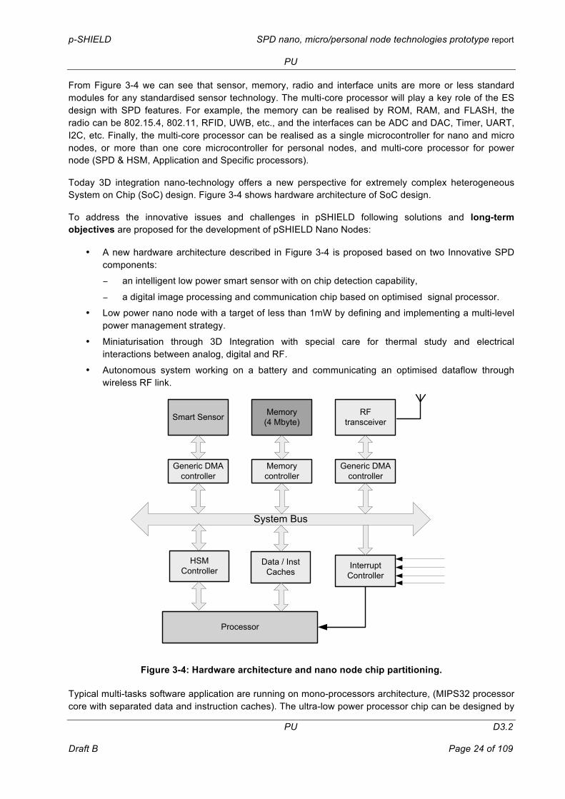
From Figure 3-4 we can see that sensor, memory, radio and interface units are more or less standard modules for any standardised sensor technology. The multi-core processor will play a key role of the ES design with SPD features. For example, the memory can be realised by ROM, RAM, and FLASH, the radio can be 802.15.4, 802.11, RFID, UWB, etc., and the interfaces can be ADC and DAC, Timer, UART, I2C, etc. Finally, the multi-core processor can be realised as a single microcontroller for nano and micro nodes, or more than one core microcontroller for personal nodes, and multi-core processor for power node (SPD & HSM, Application and Specific processors).
Today 3D integration nano-technology offers a new perspective for extremely complex heterogeneous System on Chip (SoC) design. Figure 3-4 shows hardware architecture of SoC design.
To address the innovative issues and challenges in pSHIELD following solutions and long-term objectives are proposed for the development of pSHIELD Nano Nodes:
• A new hardware architecture described in Figure 3-4 is proposed based on two Innovative SPD components:
− an intelligent low power smart sensor with on chip detection capability,
− a digital image processing and communication chip based on optimised signal processor.
• Low power nano node with a target of less than 1mW by defining and implementing a multi-level power management strategy.
• Miniaturisation through 3D Integration with special care for thermal study and electrical interactions between analog, digital and RF.
• Autonomous system working on a battery and communicating an optimised dataflow through wireless RF link.
Figure 3-4: Hardware architecture and nano node chip partitioning.
Typical multi-tasks software application are running on mono-processors architecture, (MIPS32 processor core with separated data and instruction caches). The ultra-low power processor chip can be designed by
Processor
System Bus
Generic DMA controller
Memory controller
Generic DMA controller
Data / InstCaches
Interrupt Controller
Smart Sensor Memory (4 Mbyte)
RF transceiver
HSMController
p-SHIELD SPD nano, micro/personal node technologies prototype report
PU
PU D3.2
Draft B Page 25 of 109
using VHDL (Very high speed integrated circuits Hardware Description Language). It contains also many digital peripherals like timers, watchdogs, interrupt controllers, HSM controller, UART (Universal Asynchronous Receiver/Transmitter), SPI (Serial Peripheral Interface), DMA (Direct Memory Access) controllers and interfaces/controllers to memories and cache memories. The design will also be performed taking into account the constraints of 3D integration.
3.4.1.1 SPD models
Triverdi et al. present a classification of dependability and security model types: combinatorial models, state-space models, hierarchical models, fixed point iterative model, simulation, analytic and simulation, and hybrid model, that can be applied for the presentation of dependability and security models11. For extremely difficult models analytic and simulation devices can be used in combination with the hybrid models. Development of new SPD ESDs requires careful approach and a consideration of a variety of aspects that are influencing our design methodology. Dependability and security models are developed almost independently in the area of small networked sensors. Based on the recent paper publish by Triverdi et all, called Dependability and Security Models12 we have a solid background for modelling security and dependability for SPD.
Security is a property of a system or service. Software-intensive systems are complex, meaning that they are composed of many components of different types which interact with each other to create properties not exhibited by the individual components. The purpose of the system is implemented as the service the system, acting as a provider, delivers to another system, the user system. A particular service can fail in a variety of ways, resulting in dependability being a composite property, covering the following more specific properties (more of the property is indicative of fewer or absence of the corresponding failures). Dependability and security overlap in the sense that some types of failure fall under both properties. The definition of dependability and security as the ability to avoid failures raises the question of how a system or service can be measured with regard to such ability. Deliverables D.2.2.1 and D2.2.2 addresses two fundamental concepts for SPD metrics used in pSHIELD.
3.4.2 NMP node operating systems
Selection of the operating system (OS) for the demonstrator is an important design constraint, since we need to decide in which sensor prototype platform will be realised SPD functionalities. The only requirement that we posed for this operating system is related to it’s possibility to be designed for embedded devices. There are two candidates for that: TinyOS and Contiki
3.4.2.1 Node operation systems
3.4.2.1.1 TinyOS
This operating system (OS) is a free and open source operating system and platform that is designed for WSNs. It is an embedded operating system, written in the nesC Programming language as a set of cooperating tasks and processes. NesC is actually a dialect of the C programming language that is optimised for the memory limitation of the sensor networks. TinyOS features summary:
• No Kernel: Direct hardware manipulation.
• No Process Management: Only one process on the fly.
• No Virtual Memory: Single linear physical address space.
11 K.S. Triverdi et al., “Dependability and Security Models,” 7th Int. Workshop on the Design of Reliable Communication networks (DRCN 2009), Washington DC, October 2009.
12 Kishor S. Triverdi et all, “Dependability and Security Models,” 7th International Workshop on the design of Reliable Communication Networks, DRCN 2009, Washington Dc, October 2009.

p-SHIELD SPD nano, micro/personal node technologies prototype report
PU
PU D3.2
Draft B Page 26 of 109
• No S/w Signal or Exception: Function call instead.
• No User Interface, power constrained.
• Unusually application specific H/w and S/w.
• Multiple flows, concurrency intensive bursts.
• Extremely passive vigilance (power saving).
• Tightly coupled with the application.
• Simulator: TOSSIM, PowerTOSSIM
• Written in “nesC” Language, a dialect of the ‘C’ language.
3.4.2.1.2 Contiki Operating System
Contiki is also an open source, highly portable, multi-tasking operating system for memory-efficient networked ESDs and WSNs. It is mainly designed for a microcontroller with small amount of memory. The key advantage of Contiki OS is its IP communications (both IPv4 and IPv6). It is flexible for a choice between full IP networking and low-power radio communication mechanisms. Contiki is written in the C programming language and consists of an event-driven kernel, on top of which application programs can be dynamically loaded and unloaded at run time. Contiki has been ported to different hardware platforms, such as MSP430, AVR, HC 12, and Z80. Contiki features summary:
• Event-driven Kernel: reduce the size of the system. • Pre-emptive multi-threading support: an application library that runs on top of the event-driven
kernel is optionally linked with applications that explicitly require a multithreaded model of computation.
• Simulator: COOJA • Written in ‘C’ Language.

p-SHIELD SPD nano, micro/personal node technologies prototype report
PU
PU D3.2
Draft B Page 27 of 109
4 Wireless Sensor Networks The pSHIELD network architecture for the railway application scenario, the concept of four functional layers with SPD functionalities and core services is a homogenous network as in Figure 2.2 of the Technical Annex. By introducing more implicational scenarios as in nSHIELD and Legacy ES nodes and Legacy ES Networks, the final architecture becomes a hybrid heterogeneous network (HHN). It is heterogeneous in the sense of coexistence different technologies (IEEE 802.15.4, IEEE 802.11, UMTS, etc., multi-frequency, multi- technology, multi-layer, multi-architecture) that are connected with unified control and optimisation, and it is hybrid in the sense of a network that is between a centralised and pure decentralised architecture. Figure 4-1 illustrates a WSN composed of Nano, Micro/Personal and Power Node which can be used also as a Gateway.
or Power Node
Figure 4-1: WSN composed of NMP and power nodes.
For example, in the pSHIELD network it can be designed to track wagons that pass through certain geographical areas up to the destination. Therefore, the network may switch between being a monitoring network (inside the wagons, or trains) and a data collection network (outside, railway road or railway track). During the long periods of inactivity when no monitored wagons are present, the network will simply perform the monitoring function. Each NMP or power node will monitor its sensors waiting to detect an alarm. Once an alarm event is detected, all or part of the network, will switch into a data collection network and periodically report sensor readings up to a GW that tracks the wagon. Due to this multi-modal network behaviour, it is important to develop a single architecture that can handle these application scenarios as well as other scenarios.
The final deliverables D2.1.2 (system requirements and specification) and D2.2.2 (system metrics) constrained the implementation architectural design of the NMP node on a system level with some particularities for each functional layer (node, network, middleware and overlay). D2.1.2 provides a set of system requirements specification starting with the application scenario and followed by the functional layers. D2.2.2 gives us two fundamental and complementary concepts for defining SPD metrics. However, for the pilot project we are concentrating upon the research effort on the WSNs because they are

p-SHIELD SPD nano, micro/personal node technologies prototype report
PU
PU D3.2
Draft B Page 28 of 109
excellent candidates for many application scenarios. Therefore, the SPD metrics addressed in this document are related to WSNs and its nodes.
4.1 Sensor nodes in WSNs
NMPS-SPD and/or Legacy nodes that form WSNs are so important for pSHIELD and similar systems and networks, because the following relation is showing that:
Sensing + CPU + Radio = Thousands of potential applications
The emerging field of wireless sensor networks combines sensing, computation, and communication (SCC) into a single NMP ED (NMPS or Legacy sensor). While the capabilities of any single device are minimal, the composition of hundreds of NMP EDs offers radical new technological possibilities. For example TinyOS enables us to use a hardware architecture that has a single processor time shared between both application and protocol processing. A HW and SW platform can be developed to validate a generalised architecture. The general architecture contains sensor(s), controller(s), protocol-level processing (Processor), and RF transceiver as in Figure 3-4.
The current sensor platforms do not provide sufficient SPD mechanisms. For example, if we would like to use specific cryptography operations for security purposes it requires an additional mechanism to achieve certain SPD level. In order to improve security of the NMP nodes at the operating system (OS) level, a solution should be micro-kernel based architecture. Such architecture aims to integrate various components and to establish various comportments on a single NMP platform. These comportments can be separated, but the information flow can be controlled. Each component may have its own security policy. Designing NMP nodes in this way we can allow protection of sensitive data such as cryptographic keys even if parts of the NMP node are compromised. The NMP node can be designed in such a way that a control layer composed of a microkernel and resource management/access control can take care for trusted (i.e., trusted sensor and it strongly separate security services) and untrusted (Linux, TinyOS, Contiki) SW components. Variety of the existing sensor platforms for WSNs introduced different approaches for handling SPD. This results in increasing complexity when an unified architecture design for NMP nodes is required especially when we considered different security attacks and dependability in multiple layers so that if a layer fails, the next one can take over. This approach can offer protection in diversity at relative low cost. In the following section we will summarise some key threats for WSNs.
The Wireless Sensor Networks (WSN) applications are used in many critical tasks, like aerospace, automation, monitoring environment, etc. Nowadays, these applications include new properties, such us security, dependability, privacy and trust. For WSNs applications to make security and dependability satisfaction is more and more important. In general WSNs are layered in 5 layers. In the pSHIELD project we follow the concept of four functional layers and based on that we are constructing a new type of network that we simple call it SPD network. Heterogeneity of this SPD network is an extremely important feature of the pSHIELD network, since it allows existence of different type of ESDs on the node layer.
In general, the software part of WSNs can be layered into three levels: sensor software, node software and sensor network software. Sensor software has full access to sensor hardware. The output of a function of sensor software is used by sensor node software. This level includes system software for network maintenance and for some specific applications. For example, middleware resides over the operating system. Application programs use this middleware according to their own specific requirements. So, bottom layer consists of sensor, CPU and radio, on top we have operating system and on top of them Services and applications.
There are two approaches for sensor applications:
- Service-oriented architecture (SOA) and

p-SHIELD SPD nano, micro/personal node technologies prototype report
PU
PU D3.2
Draft B Page 29 of 109
- Agent- oriented architecture (AOA).
SOA is a design approach that defines the interaction among architectural elements in terms of services that can be accessed without knowledge of the underlying platform implementation. AOA proposes an infrastructure that applies active agent technology to WSNs, because the network must be dynamically configurable and adaptive in order to response actively to events where security and dependability must be built into WSNs at the early design stage. The pSHIELD solution leverage this two approaches investigating a hybrid solution where the SOA is applied by the pSHIELD Middleware Adapter and AOA is applied by the Security Agents operating in the pSHIELD Overlay.
4.1.1 Middleware
The sensor node for standardised WSNs differs so much in terms of HW platforms. Writing an OS that runs on all these sensor platforms is impossible. To hide the underlying platform differences and to decouple the OS from HW platform a middleware is needed. The concept of middleware in distributed systems is often taken to mean the software layer that lies between the operating system and the applications on each site of the system. It facilitates scalability, interoperability, deployment, and development of applications.
In the last decade numerous works on middleware for mobile devices (smart phones) are performed and successfully implemented. Most of those devices use operating systems like Windows CE, Palm OS, Symbian OS, Tiny Linux, etc. But in this document we focus on middleware for NMP nodes, which are much smaller than those devices. The recent development of sensor node middleware is showing that we have quite a large number of middleware for WSNs. Most of the middleware we have studied are built on top of TinyOS. There are other OSs like Contiki, Mantis, SOS, and t-kernel. It is important to note that the scope of middleware for WSN is not restricted to the sensor network alone, but also covers external networks connected to the WSN (such as Internet) as well as the applications interested in querying sensor data through such external network. Standards such as 6LoWPAN (which used IEEE 802.15.4) and Web Services running directly on the sensor node allow integrating them into the Internet of Things (IoT). However, nodes which are capable to run the internet stack directly are either very expensive or not very energy-efficient. There have been several efforts to implement the Internet Protocol Stack on small energy-constrained devices. The LoWPAN and 6LoWPAN protocols try to port the IPv4 and IPv6 Protocols on small devices. This enables running services on the application layer directly on sensor nodes. The Web service technology is often used to connect and access sensors and actuators through the Internet.
The recent middleware approaches use different technique. For example, such middleware are Sensorpedia (Web 2.0 based), TinyDB (Database oriented), Mate (Virtual Machine based), Agilla (Mobile Agent), TinyLime (tuple space) and TinyCubus (cross-layered).
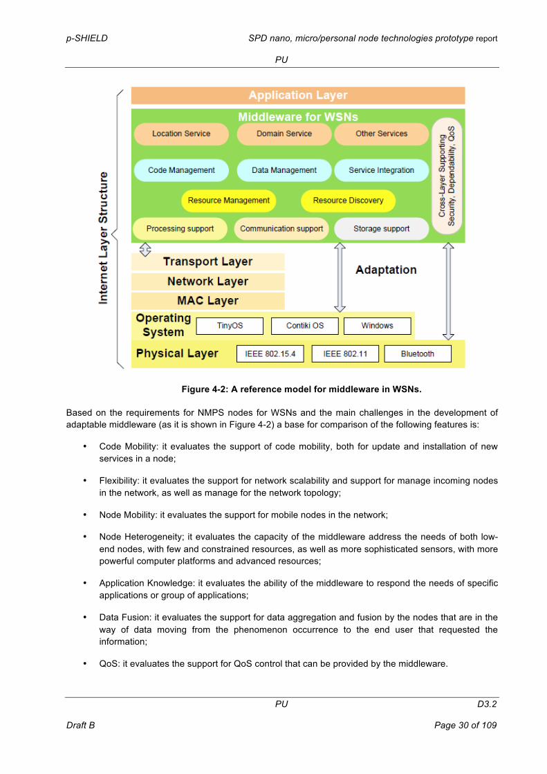
Taking in consideration that pSHIELD SPD network is composed of SPD and Legacy Nodes it is obvious that we have a complex HHN structure where the standard OSI layers are defining the overall network requirements in sense of the HW & SW components. On the physical layer (PHY) different NMP nodes will coexist in the same pSHIELD network. Above PHY different protocol stacks for different Legacy NMP nodes are increasing the complexity of the overall pSHIELD network design. Figure 4-2 illustrates a standard Internet Layer Structure and Middleware for WSNs composed of SW components that adapt the PHY layer to the application layer.
p-SHIELD SPD nano, micro/personal node technologies prototype report
PU
PU D3.2
Draft B Page 30 of 109
Figure 4-2: A reference model for middleware in WSNs.
Based on the requirements for NMPS nodes for WSNs and the main challenges in the development of adaptable middleware (as it is shown in Figure 4-2) a base for comparison of the following features is:
• Code Mobility: it evaluates the support of code mobility, both for update and installation of new services in a node;
• Flexibility: it evaluates the support for network scalability and support for manage incoming nodes in the network, as well as manage for the network topology;
• Node Mobility: it evaluates the support for mobile nodes in the network;
• Node Heterogeneity; it evaluates the capacity of the middleware address the needs of both low-end nodes, with few and constrained resources, as well as more sophisticated sensors, with more powerful computer platforms and advanced resources;
• Application Knowledge: it evaluates the ability of the middleware to respond the needs of specific applications or group of applications;
• Data Fusion: it evaluates the support for data aggregation and fusion by the nodes that are in the way of data moving from the phenomenon occurrence to the end user that requested the information;
• QoS: it evaluates the support for QoS control that can be provided by the middleware.
p-SHIELD SPD nano, micro/personal node technologies prototype report
PU
PU D3.2
Draft B Page 31 of 109
By comparing some adaptable middlewares13 like DAVIM, ATLAS, AGILLA, IMPALA, SINA, TinyCubs, MiLAN, SensorWare, TinyLime, and AWARE, the conclusion that can be drawn from this analysis is that there is a need to integrate the support for each of the described feature a common middleware platform in order to offer the required support for new emerging applications. There have been also some efforts to architect middleware for WSNs using SOA (RUNES, P2PComp, etc). SOA can deal with aspects of heterogeneity, mobility and adaptation, and offers seamless integration of wired and wireless environments.
The OSGi (Open Services Gateway Initiative) is focused on the application layer. It is open to almost any protocol, transport or device layers. The OSGi mission is multiple services, wide area networks, and local networks and devices. The OSGi advantages are platform and application independent. The central component of the OSGi specification effort is the services gateway. Service semantics for WSNs is another important issue, in addition to the service definition, so that services can be coordinated in the space.
Hydra platform14 is a new concept that is realised in such a way that between physical and application layer is a middleware. The main goal was to develop a middleware that is 'inclusive' which means that it will be possible to enable any device to be detectable and usable from a Hydra application. The concept is based on the work of Rozanski and Woods15 , and the Hydra architectural descriptions are in line with the IEEE 1471 standard. For the NMP prototype platform design concept we will explain in the following section how it can be composed by an operating system, middleware and the application layer.
The European Hydra project developed a "Middleware for Heterogeneous Physical Devices" with the aim to help manufacturers and systems integrators to build devices that can be networked easily and flexibly to create cost-effective high performance solutions. For the heterogeneous devices, sensors and actuators envisioned in the pSHIELD project, the large number of manufacturers and Universities are involved and the differences in their speed of innovation become an obstacle for the overall system design. Therefore, there is an urgent need for technologies and tools that make it easier to reap the benefits of networked systems. The complexity to build new technologies and tools grows exponentially with the number of devices, manufacturers and protocols involved.
The Hydra middleware as in Figure 4-3 is a core technology that has a transparent communication layer, equally supporting centralised and distributed architectures. The Hydra middleware takes security and trust into account and allows building model-guided web services. It runs on wired or wireless networks of distributed devices with limited resources. The embedded and mobile service-oriented architecture will provide fully compatible data access across heterogeneous platforms, allowing true ambient intelligence for networked ESDs. Adding extended security, privacy, trust and new dependability modules may satisfy requirements for having a middleware that will be SPD composable with the rest of the pSHIELD system architecture and network. The Hydra middleware consists of large number of software components – or managers – that handle various tasks needed to support cost-effective development of intelligent applications for networked embedded devices.
13 Pignaton de Freitas, “A Survey for Adaptable Middleware for Wireless Sensor Networks, Technical Report, 2008.
14 http://www.hydramiddleware.eu/news.php
15 Rozanski, N. and Woods, E. , “Software systems architecture: working with stakeholders using viewpoints and perspectives,” Pearson Education.
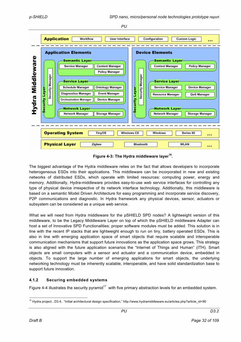
p-SHIELD SPD nano, micro/personal node technologies prototype report
PU
PU D3.2
Draft B Page 32 of 109
Figure 4-3: The Hydra middleware layer16.
The biggest advantage of the Hydra middleware relies on the fact that allows developers to incorporate heterogeneous ESDs into their applications. This middleware can be incorporated in new and existing networks of distributed ESDs, which operate with limited resources: computing power, energy and memory. Additionally, Hydra-middleware provides easy-to-use web service interfaces for controlling any type of physical device irrespective of its network interface technology. Additionally, this middleware is based on a semantic Model Driven Architecture for easy programming and incorporate service discovery, P2P communications and diagnostic. In Hydra framework any physical devices, sensor, actuators or subsystem can be considered as a unique web service.
What we will need from Hydra middleware for the pSHIELD SPD nodes? A lightweight version of this middleware, to be the Legacy Middleware Layer on top of which the pSHIELD middleware Adapter can host a set of Innovative SPD Functionalities: proper software modules must be added. This solution is in line with the recent IP stacks that are lightweight enough to run on tiny, battery operated ESDs. This is also in line with emerging application space of smart objects that require scalable and interoperable communication mechanisms that support future innovations as the application space grows. This strategy is also aligned with the future application scenarios the “Internet of Things and Human” (ITH). Smart objects are small computers with a sensor and actuator and a communication device, embedded in objects. To support the large number of emerging applications for smart objects, the underlying networking technology must be inherently scalable, interoperable, and have solid standardization base to support future innovation.
4.1.2 Securing embedded systems
Figure 4-4 illustrates the security pyramid17 with five primary abstraction levels for an embedded system.
16 Hydra project , D3.4, “Initial architectural design specification,” http://www.hydramiddleware.eu/articles.php?article_id=90

p-SHIELD SPD nano, micro/personal node technologies prototype report
PU
PU D3.2
Draft B Page 33 of 109
Confidentiality, Integrity, Authentication
Protocol
Algorithm
Architecture
Microrchitecture
Circuit
Nano nodeMicro/Personal node
Power node
Coprocessor
Key storageMicroprocessor
Embedded SW (C, Java), Security partitioning ...
RSA, ECC, HECC, AES, 3-DES, SHA-512,
RIPEMD-160
Figure 4-4: Embedded security pyramid.
The five abstraction levels are:
• Protocol level includes the protocols to be performed on embedded devices. For achieving security CIAA concept can be implemented.
• Algorithm level includes cryptographic primitives (such as Public Key, Symmetric Key crypto algorithms and hash functions) and application-specific algorithms used at the protocol level.
• Architecture level includes secure hardware/software partitioning and embedded software techniques to prevent software hacks.
• Microarchitecture deals with the hardware design of modules (the processors and coprocessors) required and specified at the architecture level.
• Circuit level requires implementing transistor level and package-level techniques to thwart various physical-layer attacks.
Protocol level is application specific and includes the design of protocols to be performed on EDs. The PKC (public key cryptosystems) are based on RSA18 or DSA19. ECC (Elliptic Curve Cryptography) and 17 D. Hwang, P. Schaumont, K. Tiri, and I. Verbauwhede. Securing Embedded Systems. In IEEE Security and Privacy Magazine 4, pages 40–49, 2006
18 R. L. Rivest, A. Shamir, and L. Adleman. A method for obtaining digital signatures and public-key cryptosystems. Communications of the ACM, 21(2):120–126, 1978.
19 A. Menezes, P. van Oorschot, and S. Vanstone. Handbook of Applied Cryptography. CRC Press, 1997.

p-SHIELD SPD nano, micro/personal node technologies prototype report
PU
PU D3.2
Draft B Page 34 of 109
Hyper-ECC (HECC) are based on different algebraic structure20. After 20 years of intensive investigation on both, theoretical and practical aspects it is evident that ECC and HECC offer equivalent security as RSA, but for much smaller key size! This result in smaller HW and lower power consumption that is extremely important for NMPS nodes. Modular multiplication forms the basis of modular exponentiation which is the core operation for RSA cryptosystems. Similarly, it is also important for ECCs especially if one use projective coordinates. Montgomery’s methods21 is the most popular for modular multiplication since it avoid time consuming trial division that is common bottleneck of other algorithms. However, it is not enough to have strong cryptographic algorithms. It is also important their implementation that must be secured. The attacks techniques are related to the PHY implementation. For example, the attack can be active or passive. Active attack is performed in such way to alters HW or SW by changing the operating conditions (power supply, temperature, etc.) Passive attack is based on monitoring side-channel information (power supply, EM radiation).
With this short introduction on pyramid security approach for ESs is clear that all abstraction level must be secured. This is a complex security approach, which can be extended to a general pyramid SPD approach for the future ESs. For the pilot pSHIELD project we focus mainly on the security aspects for ESs.
4.1.3 General security requirements
The application area for pSHIELD is security monitoring RT of dangerous materials. Security monitoring WSNs are composed of NMP and power nodes (see Figure 4-1) that are placed at fixed locations throughout an environment that continually monitor one or more sensors to detect an anomaly. Security WSNs are not actually collecting any data. For the environmental monitoring the collection of data is fundamental. Thus, for security WSNs for which data collection is not a primary goal, this has a significant impact on the optimal network architecture. Each node has to frequently check the status of its sensors but it only has to transmit a data report when there is a security violation. Once detected, a security violation must be communicated immediately to the power node and/or Gateway (GW) that is connected with the security control centre. The latency of the data communication across the WSNs to the GW has a critical impact on application performance. The end-users demand that alarm situations should be reported within seconds of detection. This means that NMP nodes must be able to respond quickly to requests from their neighbours to forward data. In security WSNs reducing the latency of an alarm transmission is significantly more important than reducing the energy cost of the transmissions. This is because alarm events are expected to be rare. When an event is present a significant amount of energy could be dedicated to the transmission. Reducing the transmission latency leads to higher energy consumption because routing nodes must monitor the radio channel more frequently. Therefore, in security WSNs, a vast majority of the energy will be spend on confirming the functionality of neighbouring nodes and in being prepared to instantly forward alarm announcements. Actual data transmission will consume a small fraction of the network energy.
The most important security requirements for WSNs are related to the CIAA (Confidentiality, Integrity, Authenticity and Availability) attributes. Measurable Security and Dependability attributes are integrity and availability. Immeasurable attributes are confidentiality and authenticity. For achieving secure
20 V. Miller. Uses of elliptic curves in cryptography. In H. C. Williams, editor, Advances in Cryptology: Proceedings of CRYPTO’85, number 218 in Lecture Notes in Computer Science, pages 417–426. Springer-Verlag, 1985, and
N. Koblitz. Elliptic curve cryptosystem. Math. Comp., 48:203–209, 1987, and N. Koblitz. A family of Jacobians suitable for Discrete Log Cryptosystems. In S. Goldwasser, editor, Advances in Cryptology: Proceedings of CRYPTO’88, number 403 in Lecture Notes in Computer Science, pages 94–99. Springer-Verlag, 1988.
21 P. Montgomery. Modular multiplication without trial division. Mathematics of Computation, 44(170):519–521, 1985.

p-SHIELD SPD nano, micro/personal node technologies prototype report
PU
PU D3.2
Draft B Page 35 of 109
communications for WSNs all messages have to be encrypted and authenticated. In the following sections we will briefly introduced the key security definitions and threats for WSNs.
4.1.3.1 Key security aspects for WSNs
4.1.3.1.1 Definitions
ACCESS CONTROL: Access control ensures that resources are only granted to those users who are entitled to them.
AUTHENTICATION: Verifying the identity of a user, process, or device, often as a prerequisite to allowing access to resources in an information system.
AVAILABILITY: Ensuring timely and reliable access to and use of information.
CONFIDENTIALITY: Preserving authorized restrictions on information access and disclosure, including means for protecting personal privacy and proprietary information.
HELLO ATTACK: An attack in which an adversary attacks the network by repeatedly transmitting HELLO messages and thereby depletes the network's resources.
INTEGRITY: Guarding against improper information modification or destruction, and includes ensuring information non-repudiation and authenticity.
SECURITY OF INFORMATION: Appropriate technical and organizational measures to ensure an appropriate level of security in relation to the risks represented by the processing and the nature of the personal data to be protected.
SPOOFING: a spoofing attack is a situation in which one person or program successfully masquerades as another by falsifying data and thereby gaining an illegitimate advantage.
SYBIL ATTACK: An attack in which the attacker subverts the reputation system of a peer to peer network by creating a large number of pseudonymous entities, using them to gain a disproportionately large influence
THREAT: Any circumstance or event with the potential to adversely impact organizational operations, organizational assets, or individuals through an information system via unauthorized access, destruction, disclosure, modification of information, and/or denial of service.
VULNERABILITY: Weakness in an information system, system security procedures, internal controls, or implementation that could be exploited or triggered by a threat source.
WORMHOLE: A particularly severe attack on routing protocols in ad hoc networks, in which two or more colluding attackers record packets at one location, and tunnel them to another location for a replay at that remote location.
4.1.3.2 Typical threats in WSNs
The security requirements for pSHIELD WSNs are similar to those of wireless ad hoc networks due to their similarities22,23. Communications over radio channels are in most of the cases insecure and easily susceptible to various kinds of threats. For WSNs composed of a high number of sensors, it is impractical
22 K. Lu e tal., » A framework for a Distributed Key Management Scheme in Heterogeneous Wireless Sensor Networks,” IEEE Trans. on Wireless Communications, vol. 7, no. 2, Feb. 2008, pp. 639-647.
23 Al-Sakib Khan Pathan e tal., “Security in Wireless Sensor Networks: Issues and Challenges,” 2007.
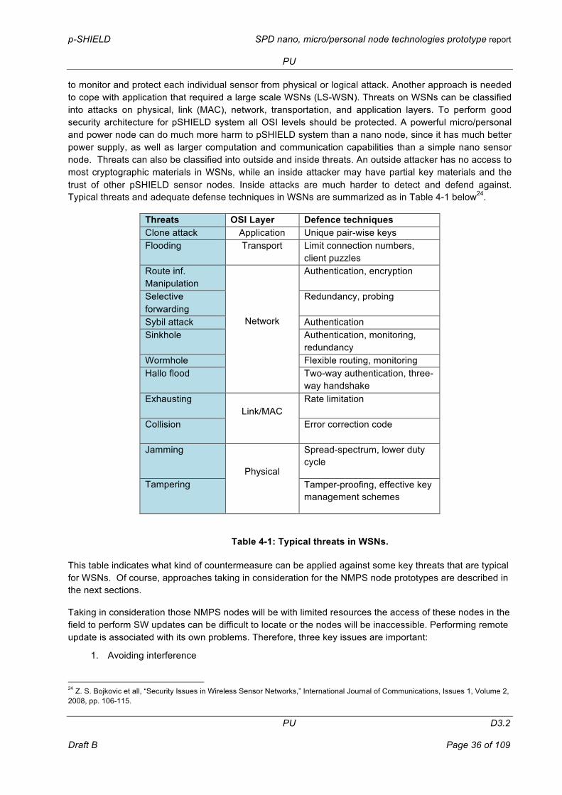
p-SHIELD SPD nano, micro/personal node technologies prototype report
PU
PU D3.2
Draft B Page 36 of 109
to monitor and protect each individual sensor from physical or logical attack. Another approach is needed to cope with application that required a large scale WSNs (LS-WSN). Threats on WSNs can be classified into attacks on physical, link (MAC), network, transportation, and application layers. To perform good security architecture for pSHIELD system all OSI levels should be protected. A powerful micro/personal and power node can do much more harm to pSHIELD system than a nano node, since it has much better power supply, as well as larger computation and communication capabilities than a simple nano sensor node. Threats can also be classified into outside and inside threats. An outside attacker has no access to most cryptographic materials in WSNs, while an inside attacker may have partial key materials and the trust of other pSHIELD sensor nodes. Inside attacks are much harder to detect and defend against. Typical threats and adequate defense techniques in WSNs are summarized as in Table 4-1 below24.
Threats OSI Layer Defence techniques Clone attack Application Unique pair-wise keys Flooding Transport Limit connection numbers,
client puzzles Route inf. Manipulation
Network
Authentication, encryption
Selective forwarding
Redundancy, probing
Sybil attack Authentication Sinkhole Authentication, monitoring,
redundancy Wormhole Flexible routing, monitoring Hallo flood Two-way authentication, three-
way handshake Exhausting
Link/MAC
Rate limitation
Collision
Error correction code
Jamming
Physical
Spread-spectrum, lower duty cycle
Tampering Tamper-proofing, effective key management schemes
Table 4-1: Typical threats in WSNs.
This table indicates what kind of countermeasure can be applied against some key threats that are typical for WSNs. Of course, approaches taking in consideration for the NMPS node prototypes are described in the next sections.
Taking in consideration those NMPS nodes will be with limited resources the access of these nodes in the field to perform SW updates can be difficult to locate or the nodes will be inaccessible. Performing remote update is associated with its own problems. Therefore, three key issues are important:
1. Avoiding interference
24 Z. S. Bojkovic et all, “Security Issues in Wireless Sensor Networks,” International Journal of Communications, Issues 1, Volume 2, 2008, pp. 106-115.

p-SHIELD SPD nano, micro/personal node technologies prototype report
PU
PU D3.2
Draft B Page 37 of 109
2. Minimizing the cost of upgrades
3. Avoiding the loss of part or all of a WSN
Figure 4-5 shows SW update model. There are three elements for SW updates with a flow from Generation (host), propagation (network) and activation (node). WSNs will be developed dynamically over time since in this field we have dramatically changes and improvements in the last five years. Standards and realises are upgraded with new features, algorithms and protocols that are evolving. This is an important driver for designing NMPS nodes and WSNs with such nodes that allow SW updates since this is a critical issues in the effective deployment of these networks as part of the pSHIELD network.
NMPS nodes, which are designed with five layers (PHY, link/MAC, network, transport and application) most of the important features and SPD functionalities will be included in the middleware to build up and maintain the network. For example routing, looking for the nodes, discovery services and self-localisation. SW updates become important for many reasons: maintenance realises, minor realises, major realises, technology insertion, etc.
Basically for WSN we identified some fundamental design constraints such as security and reliability, routing and transport, and in-networking processing.
Propagation
Generation
Activation Node
Network
Host
Update
UpdateFe
edba
ck
Figure 4-5: SW update model for WSNs.
First, the configuration of WSNs that are part of the pSHIELD network must be flexible enough to cope with abruptly disappearing nodes. The system must support routing and multiple levels of in-network processing. The second important issue is data aggregation. It is related to both the energy consumption at the sensor nodes and the effect of physical attacks on the node. To cope with this threat we need End-to-End (E2E) encryption from the NMP sensors to the sinks. This is also concerned for multicast traffic Concealed data aggregation provides a good balance between energy-efficiency and security. Data aggregation can be based on deviation query and multiple monitoring sensors. In some applications data must be stored in a distributed way. Since WSN is volatile with nodes that disappear over time, security must be combined with replication, taking space- and energy-efficiency storage. Resilient data aggregation at nodes addresses robustness against modified data. The solution must include both sensors and sink. Third, enhanced key pre-distribution is important because for the manufactures it is not possible to configure all the sensitive information before the WSN is deployed. Four, routing is one of the most important functionality of WSNs. The presence of malicious nodes must be taken in consideration and countermeasure must be applied for most of the known threats and attacks. Five, pairwise/groupwise authentication is important for establishing pair-wise relationships. For example, on top of CIAA security

p-SHIELD SPD nano, micro/personal node technologies prototype report
PU
PU D3.2
Draft B Page 38 of 109
concept, Hop-by-Hop (HbyH) authentication offers strong security mechanisms. Finally, WSN access control is essential to provide an access control for end-users of WSN applications. This helps to monitor data for authorised users only. S
4.1.4 Multidimensional metric space
This section considers the SPD metrics as in D2.1.2 and D2.2.2 with key security & dependability attributes: availability, reliability, safety, confidentiality, integrity and maintainability and the system performance metrics that are important for WSN applications such as computational time, memory size, energy consumption and cost. Additionally, authenticity attribute is very important for WSN.
The key metrics for wireless sensor networks are grouped for SPD functions
• security,
• privacy, and
• dependability,
and basic functions:
• lifetime,
• coverage,
• cost and deployment,
• response time,
• temporal accuracy, and
• effective sample rate.
These functions can be considered with the key aspects: threats, attributes and means in the main concept taxonomies: security, dependability, fault-tolerance, reliability and survivability (see D2.2.2). The importance of these functions is briefly discussed below. Many of these evaluation metrics are interrelated. For example, it may be necessary to decrease performance in one metric, such as sample rate, in order to increase another, such as lifetime. Taken together, this set of metrics form a multidimensional metric space (MMS) that can be used to describe the capabilities of a WSN and its nodes. The SPD capabilities of a prototype platform are represented by this MMS. A specific application deployment can be represented by a subset in this MMS. A system prototype platform can successfully perform the application if and only if the application requirements subset lies inside the capability of MMS.
4.1.4.1 SPD functionalities
Keeping the information secure can be extremely important for the pSHIELD application scenario. The WSNs should be capable of performing different SPD functionalities when they are monitoring and/or collecting protected or private information. Security becomes even more significant for railroad transportation of dangerous materials. Not only must the system maintain SPD, it must also be able authenticate data communication. For example, it should not be possible to introduce a false alarm message or to replay an old alarm message as a current one. A combination of CIA, privacy and HbyH is required to address the needs of all application scenarios. Additionally, it should not be possible to prevent proper operation by interfering with transmitted signals. Use of E2E and cryptographic authentication costs both power and network bandwidth, but it is possible today with the current nano- and mico-electronics ES devices (ESDs). However, extra computation must be performed to encrypt and
p-SHIELD SPD nano, micro/personal node technologies prototype report
PU
PU D3.2
Draft B Page 39 of 109
decrypt data and extra authentication bits must be transmitted with each packet. This impacts application performance by decreasing the number of samples than can be extracted from a given network and the expected network lifetime as we cans see in the following sections.
4.1.4.2 Lifetime
Lifetime is critical for any wireless sensor network deployment. Targeting both the rail track monitoring and security application scenarios require to have NMPS nodes placed out in the field, unattended, for months or years. Each node must be designed to manage its local supply of energy in order to maximize total network lifetime. For security requirements of the pSHIELD system, every node must last for multiple years. A single node failure would create a vulnerability in the security system. This is also demonstrating that a basic functionality like lifetime is interrelated with security. For the application scenario most of the nodes will be self-powered. They will either have to contain enough stored energy to last for years, or they will have to be able to scavenge energy from the environment through devices, such as solar cells, piezoelectric generators, or other solutions.
4.1.4.3 Coverage
The coverage is one of the primary metrics for WSNs. It is always advantageous to have the ability to deploy a network over a larger physical area (railway roads). This can significantly increase a system’s value to the end user. In theory, the coverage can be associated with the ability to extend network range. However, for a given transmission range, the networking protocols increase the power consumption of the nodes, which may decrease the network lifetime. Additionally, they require a minimal node density, which may increase the deployment cost. Therefore, the scalability is a key component of the WSNs. We can deploy a small trial network and then can continually add additional sensors to collect more information. For that we must assure that the pSHIELD network technology is capable of scaling to meet this need. Increasing the number of NMPS nodes in the system will impact either the lifetime or effective sample rate. More NMP sensors will cause more data to be transmitted which will increase the power consumption of the network.
4.1.4.4 Cost and deployment
For the pSHIELD network a key advantage is an easy deployment of WSNs. We cannot expect that end-users and workers should understand the underlying networking and communication mechanisms of WSNs. The system deployments will be successful if the wireless sensor network should configure itself. It should be possible for NMP nodes to be placed by an untrained person and have the system simply work. Ideally, the system would automatically configure itself for any possible physical NMP node placement. The real pSHIELD system must put constraints on actual NMP node placements. For the WSN prototypes we should consider the capability of providing feedback when the network and node constraints are violated. The network should be able to assess QoS and indicate any potential problems. To achieve this each NMPS node should be capable of performing link discovery and determining link quality. It may be too heavy for a nano node, but guaranteed by micro/personal and power nodes. In addition to an initial configuration phase, the system must also adapt to changing system and environmental conditions. Throughout the lifetime of a deployment, nodes may be relocated so that they interfere with the communication between two nodes. Therefore, the network should be able to automatically reconfigure on demand in order to tolerate these occurrences.
The long term strategy and total cost of ownership for a pSHIELD system may have more to do with the maintenance cost than the initial deployment cost. The security application scenario in particular requires that the system be extremely robust due to the fact that we transport dangerous materials. It is extremely important for such application to have extensive HW and SW testing prior to deployment. The system must be constructed so that it is capable of performing continual self-maintenance. When necessary, it should also be able to generate requests when external maintenance is required. For a real deployment, a
p-SHIELD SPD nano, micro/personal node technologies prototype report
PU
PU D3.2
Draft B Page 40 of 109
fraction of the total energy budget must be reserved to system maintenance and verification. However, the generation of diagnostic and reconfiguration traffic reduces the network lifetime. It can also decrease the effective sample rate.
4.1.4.5 Response time
For the pSHIELD application scenario, the system response time is a critical performance metric. An alarm must be signalled immediately when a threat, attack or intrusion is detected. Because these events will be infrequent, they may occur at any time without notice. Therefore the NMPS nodes must be capable of having immediate, high-priority messages communicated across the network as quickly as possible. Response time is also critical when security monitoring is performed, when frequently request for a status is required. In opposite to this requirement, the ability to have low response time conflicts with many of the techniques used to increase network lifetime. Network lifetime can be increased by having nodes only operate their radios for a determined period of time. If a NMPS node only turns on its radio once per minute to transmit and receive data, it would be impossible to meet the application requirements for response time of a security system. Response time can be improved by including nodes that are powered all the time. This, however, reduces an easy deployment of such system.
4.1.4.6 Temporal accuracy
The railroad tracking applications required samples from multiple nodes, which should be cross-correlated in time in order to determine the nature of phenomenon being measured. The accuracy of this correlation will depend on the rate of propagation of the phenomenon being measured. In the case of determining the average temperature of a wagon that transport such dangerous material for which we need to control temperature, samples must only be correlated to within seconds. Another case is, to determine the presence of dangerous toxic gases transported in a wagon. For that it may be required millisecond accuracy. For achieving temporal accuracy, the pSHIELD network must be capable of constructing and maintaining a global time base that can be used to chronologically order samples and events. This requires a distributed system in which energy should be expended to maintain a distributed clock. Time synchronization information should be continually communicated between nodes. The frequency of the synchronization messages is dependent on the desired accuracy of the time clock.
4.1.4.7 Effective sample rate
For the application scenarios where data collection is performed, effective sample rate is an important application performance metric. The effective sample rate is define as the sample rate that sensor data can be taken at each individual NMP sensor and communicated to a collection point (for example a micro/personal and power node) for a data collection network. In data collection applications typically demand for sampling rates is 1-2 samples per minute. Additionally to the sample rate of a NMPS, it must also consider the impact of the multi-hop networking architectures on a node ability to effectively relay the data of surrounding NMP nodes. With respect to the information importance a NMPS nodes must handle the data of all of its neighbours in a tree. For example, if a sensor transmits a single data reading and it has a total of 100 neighbours, then it will be forced to transmit 100 times as much data. Additionally, it must be capable of receiving those 100 readings in a single sample period. This multiplicative increase in data communication has a significant effect on system requirements. Thus, network bit rates combined with maximum network size end up impacting the effective per-node sample rate of the complete system25. For increasing the effective sample rate beyond the raw communication capabilities of the network is to exploit in-network processing. There are various forms of spatial and temporal compression can be used to reduce the communication bandwidth required while maintaining the same effective sampling rate. In-network data processing can be used to determine when an “important” event has occurred and automatically trigger data storage. Triggering is the simplest form of in-network processing. 25 Doherty, L., Algorithms for Position and Data Recovery in Wireless Sensor Networks. UC Berkeley EECS Masters Report, 2000.

p-SHIELD SPD nano, micro/personal node technologies prototype report
PU
PU D3.2
Draft B Page 41 of 109
This type of processing is commonly used in security systems where each individual sensor is sampled continuously, processed, and only when a security breach has occurred is data transmitted to the base station.
4.1.4.8 NMP node SPD and system metrics
Based upon the selected SPD and other system metrics, we can establish the set of metrics for pSHIELD that will be used to evaluate the performance of the network as a whole or a part of it, for example WSN. Furthermore, we can link the system performance metrics down to the individual NMP node characteristics that support them. The final goal is to understand how changes to the low-level system architecture impact application performance. Since the application metrics are often interrelated, we will see that an improvement in a node evaluation metric often comes at the expense of another one.
4.1.4.8.1 SPD metrics aspects
In order to meet the application level SPD requirements, the individual NMP nodes must be capable of performing complex encrypting and authentication algorithms. The nature of wireless communication is that is easily susceptible to interception and thus so venerable for different threats and attacks. The solution for that is to keep data in these networks private and authentic is to encrypt all data transmissions. For example, the microprocessor must be capable of performing the required SPD operations. Cryptography can be done with help of cryptographic accelerators. For securing all data transmission, the nodes themselves must secure the data that they contain. In the cases while they will not have large amounts of application data stored internally, they will have to store secret encryption keys used in the network. If these keys are revealed, the security of the network could crumble. To provide true security, it must be difficult to extract the encryption keys of from any node.
4.1.4.8.2 Power
The energy constrained operation (ultralow power) can be achieved by combining both low-power hardware components and low duty-cycle operation techniques in pSHIELD. During active operation, radio communication will constitute a significant fraction of the node’s total energy budget. Algorithms and protocols must be developed to reduce radio activity whenever possible. This can be achieved by using localized computation to reduce the streams of data being generated by NMPSs and through application specific protocols. For example, events from multiple NMPS nodes can be combined together by a local group of nodes before transmitting a single result across the WSN.
4.1.4.8.3 Flexibility
The pSHIELD network assumes that the NMP node architecture must be flexible and adaptive. Each application scenario will demand a slightly different mix of SPD and system metrics. Especially, flexibility features is important for nSHIELD where different application scenarios are considered. Therefore, for the WSN architecture included in pSHIELD it must be flexible enough to accommodate a wide range of application behaviours. For cost reasons each device will have only the HW and SW that it actually needs for a given the application. The node architecture should make it easy to assemble just the right set of SW/HW components. Thus, these devices require an unusual degree of SW/HW modularity while simultaneously maintaining efficiency.
4.1.4.8.4 Robustness
Robustness of the NMP nodes is important in a typical deployment scenario where hundreds of nodes will have to work together for a long period of time. To achieve this, the system must be constructed so that it can tolerate and adapt to individual NMP node failure. Additionally, each NMP node must be designed to be as robust as possible. To achieve this goal, system modularity is a powerful tool that can be used to develop a robust system. By dividing SPD and/or system functionality into isolated sub-elements, each function can be completely tested in isolation prior to combining them into a complete application. To

p-SHIELD SPD nano, micro/personal node technologies prototype report
PU
PU D3.2
Draft B Page 42 of 109
facilitate this, system components should be as independent as possible and have interfaces that are narrow, in order to prevent unexpected interactions. As these WSNs will often coexist with other Legacy system in the pSHIELD system, they need the ability to adapt their behaviour accordingly. The robustness of wireless links to external interference can be greatly increased through the use of techniques for heaving orthogonal radio channels (e.g., OFDM, spread spectrum).
4.1.4.8.5 Radio communication
The computation subsystem is the core of a MNPS node. It gathers data from the sensors, processes this data, decides when and where to send it, receives data from other sensor nodes, and activates the actuator accordingly. It has to execute various programs, ranging from time-critical signal processing and communication protocol stack to application programs. For any WSN use in pSHIELD the communication rate, power consumption, and range are key evaluation metric. The most application scenarios have node densities that correspond to the sensing capabilities required (granularity of the nodes deployment). If the radio communications range demands a higher node density, additional nodes must be added to the system in to increase node density to a tolerable level. The radio communication rate also has a significant impact on node performance. Higher is the communication rating a higher effective sampling rate and lower network power consumption can be achieved. As bit rates increase, transmissions take less time and therefore potentially require less energy. However, an increase in radio bit rate is often accompanied by an increase in radio power consumption. However, an increase of the communication bit rate has a significant impact on the power consumption and computational requirement of the NMP nodes.
4.1.4.8.6 Computation
The two most computationally intensive operations for an NMP node are the in-network data processing and the management of the protocols. When data is arriving over the network, the microprocessor should simultaneously control the radio and record/decode the incoming data. Higher communication rates required faster computation. The same is true for processing being performed on raw sensor data. Analog sensors can generate thousands of samples per second. The sensor processing operations include digital filtering, averaging, threshold detection, correlation and spectral analysis. It may even be necessary to perform a real-time FFT on incoming data in order to detect an event. Additionally to a locally process that refine and discard sensor readings, it can be beneficial to combine data with neighboring sensors before transmission across a network. This in-network processing requires additional computational resources.
4.1.4.8.7 Time Synchronization
In order to support time correlated sensor readings and low-duty cycle operation of pSHIELD data application scenario, NMPS nodes must be able to maintain precise time synchronization with other members of the network. To save energy the nodes need to sleep and awake together so that they can periodically communicate. Errors in the timing mechanism will create inefficiencies that result in increased duty cycles. In distributed systems, clocks drift apart over time due to inaccuracies in timekeeping mechanisms. High-precision synchronization mechanisms must be provided to continually compensate for these inaccuracies.
4.1.4.8.8 Size & Cost
The physical size and cost of each individual NMPS node has a significant and direct impact on the ease and cost of deployment of the pSHIELD network. Total cost of ownership and initial deployment cost are two key factors that will drive the adoption of WSN technologies. A reduction in per-node cost will result in the ability to purchase more MNPS nodes, deploy a security network with higher density that monitor and collect more data. Smaller NMPS nodes can be placed in more locations and used in more application scenarios. In the node tracking scenario, smaller, lower cost NMPS nodes will result in the ability to track more objects.
p-SHIELD SPD nano, micro/personal node technologies prototype report
PU
PU D3.2
Draft B Page 43 of 109
5 Firmware, Secure SoC, and Trust This chapter focus on the security aspects in WSNs and summarises the recent recommendations for SW and/or HW based security. The main enhancements security technologies for WSNs are secure ES firmware, secure and trusted boot, secure key installation, secure upgrade mechanisms, SW upgrade for NMP sensor nodes, TPM (Trusted Platform Module) and MTM (Mobile Trusted Module), Trusted Zone technologies by ARM. Security techniques in WSNs are divided as
• Hardware:
- External or extra security chip
- Security unit embedded into the CPU
- Dual virtual CPU (Trust Zone)
• Software: security algorithms installed in the MEM and used when they are needed.
5.1 Firmware
Firmware typically contains the program code that controls the underlying hardware of the system. Retrieving and analysing firmware can allow the attacker to gain a detailed understanding of the product and possibly modify code to bypass failure detection or authentication routines. This section provides some considerations for implementing in firmware to help increase the security of the overall product. Actually firmware consists of microcode programs executed from very high speed control storage. Commonly used object programs placed in ROMs and PROMs are also sometimes referred to as firmware. The problem with any approach to the field firmware updates is that if the upgrade contains a flaw, the target system may become an expensive doorstop. Many of the pitfalls are obvious and straight forward, but some insidious defects don’t appear until after a product has been deployed. Any well designed firmware upgrade system must be able to recover from user errors and other catastrophic events to the fullest extent possible.
5.1.1 Security requirements for ES firmware
Beside the standard pyramid methodology explained in Section 4.1.2 and Section 4.1.3 the security requirements may vary depending of the system perspective that we consider. Typical security requirements seen across a wide range of embedded systems, which are described as follows:
• User identification refers to the process of validating users before allowing them to use the system.
• Secure network access provides a network connection or service access only if the device is authorized.
• Secure communications functions include authenticating communicating peers, ensuring confidentiality and integrity of communicated data, preventing repudiation of a communication transaction, and protecting the identity of communicating entities.
• Secure storage mandates confidentiality and integrity of sensitive information stored in the system.
• Content security enforces the usage restrictions of the digital content stored or accessed by the system.
• Availability ensures that the system can perform its intended function and service legitimate users at all times, without being disrupted by denial-of-service (DoS) attacks.

p-SHIELD SPD nano, micro/personal node technologies prototype report
PU
PU D3.2
Draft B Page 44 of 109
Various security technologies and mechanisms have been designed around the cryptographic algorithms in order to provide specific security services. For example:
• Security protocols provide ways of ensuring secure communication channels to and from the embedded system. IPSec and SSL are popular examples of security protocols, widely used for Virtual Private Networks (VPNs) and secure web transactions, respectively.
• Digital certificates provide ways of associating identity with an entity, while biometric technologies such as fingerprint recognition and voice recognition aid in end-user authentication. Digital signatures, which function as the electronic equivalent of handwritten signatures, can be used to authenticate the source of data as well as verify its identity.
• Digital Rights Management (DRM) protocols provide secure frameworks for protecting application content against unauthorized use.
• Secure storage and secure execution require that the architecture of the system be tailored for security considerations. Simple examples include the use of HW to monitor bus transactions and block illegal accesses to protected areas in the memory, authentication of firmware that executes on the system, application isolation to preserve the privacy and integrity of code and data associated with a given application or process, HW/SW techniques to preserve the privacy and integrity of data throughout the memory hierarchy, execution of encrypted code, and so on.
The ESs need to support various security solutions in order to deal with one or more of the security requirements described earlier. These requirements present significant bottlenecks during the ES design process, which are briefly described below.
• Processing Gap: Existing embedded system architectures are not capable of keeping up with the computational demands of security processing, due to increasing data rates and complexity of security protocols. These shortcomings are most felt in systems that need to process very high data rates.
• Battery Gap: The energy consumption overheads of supporting security on battery-constrained embedded systems are very high. Slow growth rates in battery capacities (5–8% per year) are easily outpaced by the increasing energy requirements of security processing, leading to a battery gap. Various studies show that the widening battery gap would require designers to make energy-aware design choices (such as optimised security protocols, custom security hardware, and so on) for security.
• Flexibility: An embedded system is often required to execute multiple and diverse security protocols and standards in order to support multiple security. Furthermore, with security protocols being constantly targeted by hackers, it is not surprising that they keep continuously evolving. It is, therefore, desirable to allow the security architecture to be flexible (programmable) enough to adapt easily to changing requirements.
• Tamper Resistance: Attacks due to malicious software such as viruses and trojan horses are the most common threats to any embedded system that is capable of executing downloaded applications. These attacks can exploit vulnerabilities in the OS or application software, procure access to system internals, and disrupt its normal functioning. Because these attacks manipulate sensitive data or processes (integrity attacks), disclose confidential information (privacy attacks), and/or deny access to system resources (availability attacks), it is necessary to develop and deploy various HW/SW countermeasures against these attacks. Tamper resistance measures should, therefore, secure the system implementation when it is subject to various physical and side-channel attacks.
• Assurance Gap: As systems become more complicated, there are inevitably more possible failure modes that need to be addressed. Increases in embedded system complexity are making it more and more difficult for embedded system designers to be confident that they have not overlooked a serious weakness.

p-SHIELD SPD nano, micro/personal node technologies prototype report
PU
PU D3.2
Draft B Page 45 of 109
• Cost: One of the fundamental factors that influence the security architecture of an embedded system is cost. To understand the implications of a security related design choice on the overall system cost, consider the decision of incorporating physical security mechanisms in a single-chip cryptographic module.
5.1.2 Secure SoC
Based on Figure 3-1 the partition of node functionalities are the following: SS is responsible for system start-up, operating system and application, NVM has ROM, MEM has RAM, SP is dedicated for security and privacy issues like encryption/decryption, and key generation, AP is the main processor. Designing a secure NMP node require splitting some modules like NVM and MEM as it is explained also by pyramid approach. Therefore, the formal conceptual model for pSHIELD nodes requires further design considerations for achieving a more generic SPD NMP node architecture.
The Secure SoC (system on chip) as in Figure 5-1 provides physical protection to secret keys by keeping the components like secure ROM (NVM unit), which is handling the secret keys, inside the secure SoC. During execution time, the protected secure keys from the secure ROM has to be loaded to the RAM (MEM unit) in clear text and during that time the bus from the secure ROM to the RAM can be monitored to access the secret keys. This can be prevented by allocating buffers for secret keys or intermediate values of cryptographic operations involving secret keys in the internal RAM of the secure SoC. This prevents the protected keys being available to any bus outside the Secure SoC. The secure Bootloader in the secure SoC ensures that the device boots up with the genuine OS or firmware (SS unit) with right process privileges. The Memory Management Unit (MMU) configured by the OS permits the access to the buffers in the internal RAM that involves secret key operations only to the secure processes with special OS privileges. In the case where the secure ROM is limited or pre-programmed by the hardware manufacturer, the secure ROM can be programmed with a master key. This master key can be used to encrypt and store the device secret keys in the internal ROM.
Figure 5-1: A schematic view on a secure Soc architecture.
In ideal case of a Secure SoC
• The Secure ROM cannot be physically accessed to retrieve the secret keys. • The buses inside the secure SoC cannot be monitored to obtain protected data or keys.
p-SHIELD SPD nano, micro/personal node technologies prototype report
PU
PU D3.2
Draft B Page 46 of 109
• The removal or replacement of any components in the secure SoC should be impossible or should prevent the SoC from working.
5.1.3 Security in firmware updates systems
The purpose of the secure update system is to prevent malicious attackers from installing a firmware that is not approved by the manufacturer. Verifying the firmware means validating that this holds that the firmware provided for update is approved. To ensure that data sent over a communications channel is error free on arrival, a non-cryptographic checksum algorithm is typically used26. Unfortunately, these algorithms are not effective to protect from deliberate manipulation and therefore checksum algorithms are not suitable for firmware verification. One-way hash functions, also known as message digests, cryptographic checksums and message integrity check (MIC) provide message integrity27. Hash algorithms use far less resources than other cryptographic algorithms, making them suitable for resource constrained embedded systems28, but the only reason for verifying the firmware using hash functions that we can imagine is if there exists a secure channel with very restricted bandwidth on which the hash could be sent but where the transfer of the firmware image would be impractical.
A Message Authentication Code (MAC) provides both integrity and authentication and is a function that is based on a secret key, thus using symmetric cryptography. A MAC based on cryptographic hash functions, such as the one-way hash functions, is called keyed-hash based MAC, or HMAC29. Symmetric ciphers can provide confidentiality, integrity and authentication (CIA). Examples of symmetric ciphers are Data Encryption Standard (DES) and its successor Rijndael, the Advanced Encryption Standard (AES). A cryptosystem, both symmetric and asymmetric, should be secure even if an attacker knows all details about it except the secret key! The research reports show that symmetric cryptography as not suitable as the firmware verification algorithm in an updatable system.
Public key cryptography is the common name for asymmetric cryptography, and it can provide CIA. The basis is a public key used for encryption and a private key used for decryption. Public key cryptography might be suitable as firmware verification algorithm, if the firmware producer uses unique keys for each device. A better solution, that can use public key cryptography, is digital signatures. For example, protocols used for creating digital signatures are RSA, Digital Signature Algorithm (DSA) and Elliptic Curve Digital Signature Algorithm (ECDSA). We believe that digital signatures are suitable for firmware verification.
There are two typical methods for firmware updates30:
1. Micro-programmer (Figure 5-2)
2. Boot loader (Figure 5-3)
26 NIST. (2007) Recommendation for key management - part 1: General (revised). Accessed 2008-05-14. [Online]. Available: http://csrc.nist.gov/ publications/nistpubs/800-57/sp800-57-Part1-revised2_Mar08-2007.pdf
27 B. Schneier, Applied Cryptography, Second Edition. John Wiley & Sons, Inc, 1996.
28 T. Stapko, Practical Embedded Security. Newnes, 2008.
29 The Keyed-Hash Message Authentication Code (HMAC), National Institute of Standards and Technology Std., 2002. [Online]. Available: http://csrc.nist.gov/publications/fips/fips198/fips-198a.pdf
30 David Abrahamsson, “Security Enhanced Firmware Update Procedures in Embedded Systems,” PhD thesis, 2008.

p-SHIELD SPD nano, micro/personal node technologies prototype report
PU
PU D3.2
Draft B Page 47 of 109
Enter Firmware Update State
Load Firmware(microprogrammer task)
Download Microprogrammer to RAM and execute it
System
Ethernet
Install Firmware(microprogrammer task)
TFTP
Physical
Interface User
Send Microprogrammer Code
Press Button
Send Firmware Code
Figure 5-2: An exemplary flow for a firmware update process using the microprogrammer approach.
Execute firmware update procedure code
Load firmware
Install firmware
System Interface User
Physical
TFTP
Figure 5-3: An exemplary flow for a firmware update process using the boot loader approach.
5.1.4 TPM, MTM and secure boot
5.1.4.1 Trust Computing
The Trusted Computing Group (TCG) released a set of specifications for devices which enable trusted computing. TCG specifications enable a more secure computing environment to help protect and strengthened the platform against attacks, be it software attacks or physical attacks. Trusted computing, herein, refers to technologies that offer solutions to computer security through hardware enhancements and associated software modifications. TCG has also produced an implementation of the published specification in the form of a security chip called the Trusted Platform Module (TPM). The TPM provides cryptographic functions and ensures that important information such as keys, passwords and digital certificates are stored in a shielded location where it is safe from attacks. However, the TPM must be bound to the platform which makes it particularly suitable to be integrated onto a power node. For embedded and mobile applications, the TCG has released new specification, the Mobile Trusted Module

p-SHIELD SPD nano, micro/personal node technologies prototype report
PU
PU D3.2
Draft B Page 48 of 109
(MTM), which introduces the concept of “secure boot” and supports the implementation of the MTM as functionality rather than a hardware implementation for the device. Nevertheless, the resent research paper identified specific problem areas in the MTM specifications which affect power consumption and performance of cryptographic functions, among others31.
Manufacturers of the ARM processors, on the other hand, have integrated the TPM-like features directly into the processor core with the objective of achieving the security goals of the TPM specifications. Muhammad Amin et.al32 in his paper also claims that the ARM TrustZone chip is the only trusted hardware that is designed for embedded appliances.
Two fundamental TC concepts are secure boot and secure storage.
1. Secure boot guarantees that violations of integrity properties of the software stack that is booted on a platform can be prevented, i.e., software that violates the integrity properties cannot be loaded. A variant of this pattern, termed authenticated boot, does not prevent software from being loaded, but allows reliable verification of the load-time integrity of the software that has been booted later on. Secure boot is a building block at the heart of many TC-based solutions (including implementations of secure storage).
2. Secure storage is a crucial application-level requirement in many scenarios. Simple encryption is often not enough to protect sensitive data: it must also be ensured that an attacker cannot obtain the decryption key. Secure storage solves this issue by using hardware (and software) to enforce access restrictions on the stored data. Before access is granted to an application, the integrity of the software is verified.
Secure storage and secure boot are essential concepts for TC systems. For instance, a Common Criteria protection profile for security kernels with TC support has been evaluated and certified recently33, which also includes secure boot and secure storage. To protect the initial boot module (and its verification data) and to reliably build the chain of trust, the root of trust is realised in hardware. Hardware is assumed to be more secure than software because it cannot be changed or read out as easily as software. Moreover, hardware security modules can be protected against various physical attacks – at least to some extent.
Figure 5-4 shows the elements of the Secure Boot pattern. The Root of Trust for Measurement is the first module in the bootstrap chain and realised and protected by hardware. A Bootstrap Module has a link to the next Bootstrap Module, which is “measured” for its integrity (typically, by computing a hash value) before control is transferred. Each Bootstrap Module has to maintain (and protect) its corresponding integrity verification data. The verification data of the Root of Trust module is also protected by the hardware, e.g., stored in protected memory registers.
31 J. Grobschadl, T. Vejda, and D. Page, "Reassassing the TCG Specifications for Trusted Computing in Mobile Embedded Systems," in 1st IEEE Workshop on hardware-Oriented Security and Trust HOST2008, 2008, pp. 84-90. 32 M. Amin, S. Khan, T. Ali, and S. Gul, "Trends and Directions in Trusted Computing:Models, Architectures and Technologies," in International MultiConference of Engineers and Computer Scientists 2008, Hong Kong, 2008. 33 H. L¨ohr, A.-R. Sadeghi, C. St¨uble, M. Weber, and M. Winandy, “Modeling trusted computing support in a protection profile for high assurance security kernels,” in 2nd International Conference on Trusted Computing (TRUST 2009). LNCS 5471, Springer, 2009, pp. 45–62.
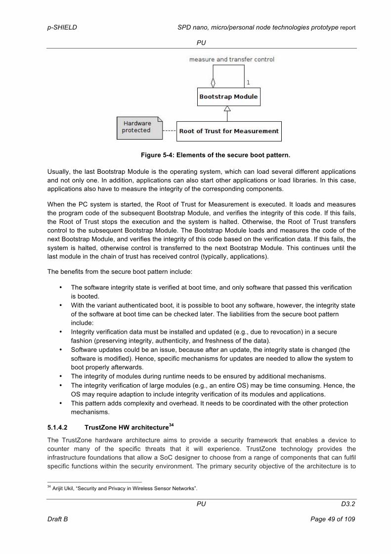
p-SHIELD SPD nano, micro/personal node technologies prototype report
PU
PU D3.2
Draft B Page 49 of 109
Figure 5-4: Elements of the secure boot pattern.
Usually, the last Bootstrap Module is the operating system, which can load several different applications and not only one. In addition, applications can also start other applications or load libraries. In this case, applications also have to measure the integrity of the corresponding components.
When the PC system is started, the Root of Trust for Measurement is executed. It loads and measures the program code of the subsequent Bootstrap Module, and verifies the integrity of this code. If this fails, the Root of Trust stops the execution and the system is halted. Otherwise, the Root of Trust transfers control to the subsequent Bootstrap Module. The Bootstrap Module loads and measures the code of the next Bootstrap Module, and verifies the integrity of this code based on the verification data. If this fails, the system is halted, otherwise control is transferred to the next Bootstrap Module. This continues until the last module in the chain of trust has received control (typically, applications).
The benefits from the secure boot pattern include:
• The software integrity state is verified at boot time, and only software that passed this verification is booted.
• With the variant authenticated boot, it is possible to boot any software, however, the integrity state of the software at boot time can be checked later. The liabilities from the secure boot pattern include:
• Integrity verification data must be installed and updated (e.g., due to revocation) in a secure fashion (preserving integrity, authenticity, and freshness of the data).
• Software updates could be an issue, because after an update, the integrity state is changed (the software is modified). Hence, specific mechanisms for updates are needed to allow the system to boot properly afterwards.
• The integrity of modules during runtime needs to be ensured by additional mechanisms. • The integrity verification of large modules (e.g., an entire OS) may be time consuming. Hence, the
OS may require adaption to include integrity verification of its modules and applications. • This pattern adds complexity and overhead. It needs to be coordinated with the other protection
mechanisms.
5.1.4.2 TrustZone HW architecture34
The TrustZone hardware architecture aims to provide a security framework that enables a device to counter many of the specific threats that it will experience. TrustZone technology provides the infrastructure foundations that allow a SoC designer to choose from a range of components that can fulfil specific functions within the security environment. The primary security objective of the architecture is to
34 Arijit Ukil, “Security and Privacy in Wireless Sensor Networks”.
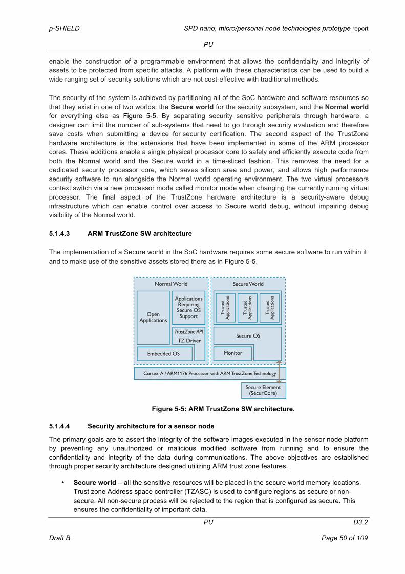
p-SHIELD SPD nano, micro/personal node technologies prototype report
PU
PU D3.2
Draft B Page 50 of 109
enable the construction of a programmable environment that allows the confidentiality and integrity of assets to be protected from specific attacks. A platform with these characteristics can be used to build a wide ranging set of security solutions which are not cost-effective with traditional methods.
The security of the system is achieved by partitioning all of the SoC hardware and software resources so that they exist in one of two worlds: the Secure world for the security subsystem, and the Normal world for everything else as Figure 5-5. By separating security sensitive peripherals through hardware, a designer can limit the number of sub-systems that need to go through security evaluation and therefore save costs when submitting a device for security certification. The second aspect of the TrustZone hardware architecture is the extensions that have been implemented in some of the ARM processor cores. These additions enable a single physical processor core to safely and efficiently execute code from both the Normal world and the Secure world in a time-sliced fashion. This removes the need for a dedicated security processor core, which saves silicon area and power, and allows high performance security software to run alongside the Normal world operating environment. The two virtual processors context switch via a new processor mode called monitor mode when changing the currently running virtual processor. The final aspect of the TrustZone hardware architecture is a security-aware debug infrastructure which can enable control over access to Secure world debug, without impairing debug visibility of the Normal world.
5.1.4.3 ARM TrustZone SW architecture
The implementation of a Secure world in the SoC hardware requires some secure software to run within it and to make use of the sensitive assets stored there as in Figure 5-5.
Figure 5-5: ARM TrustZone SW architecture.
5.1.4.4 Security architecture for a sensor node
The primary goals are to assert the integrity of the software images executed in the sensor node platform by preventing any unauthorized or malicious modified software from running and to ensure the confidentiality and integrity of the data during communications. The above objectives are established through proper security architecture designed utilizing ARM trust zone features.
• Secure world – all the sensitive resources will be placed in the secure world memory locations. Trust zone Address space controller (TZASC) is used to configure regions as secure or non-secure. All non-secure process will be rejected to the region that is configured as secure. This ensures the confidentiality of important data.

p-SHIELD SPD nano, micro/personal node technologies prototype report
PU
PU D3.2
Draft B Page 51 of 109
• Single physical core – safe and efficient execution of code from both normal and secure world. This allows high performance security software to run alongside with normal world operating environment. Secure monitor code will be developed to switch from normal to secure and vice versa.
• Secure boot – Running secure boot algorithm to ensure the integrity of the software images and devices on the platform.
• On-Soc RAM and ROM will ensure no highly sensitive data leaves the chip thus eliminating the possibility of physical attacks.
• Identity based Encryption Algorithm for confidentiality and integrity of the data during communications. (Communications between sensor node and base station)
By using ARM trust zone, a small on-chip security system is presented in Figure 5-6 below to execute the above objectives. It clearly depicts the permanent secure place and dynamic secure place that are accessible through AXI2APB bus system which has the capability to switch from secure process and non-secure process. Trust Zone Memory Adapter (TZMA) will secure a region within an on-SoC memory such as SRAM where the secure location will be in the lower part of the memory region.
Figure 5-6 proposes security architecture for sensor node using ARM11 with Trust zone features. Trust zone Address Space Controller (TZASC) will reject any non-secure transaction to a region that is configured as secure. Therefore external memory also can be partitioned into secure and non-secure region. Compared to previous works, the proposed security architecture has extended the security infrastructure throughout the system design. Instead of protecting assets in a dedicated hardware block, this architecture has made the valuable assets secured in the most protected location. On top of the hardware design, a suitable security protocol such as secure boot will also be configured to complete the security design. Secure boot with the root of trust located in On-SoC ROM will provide a chain of trust for all the secure world software and hardware peripherals and some of the normal world software. With secure boot, the integrity of the OS image, software and peripherals on the platform can be verified to be truly unadulterated. Communications right after the secure boot process can be confirmed coming from a trusted sensor node.
Figure 5-6: Security architecture for sensor node using Arm11 with Trust zone features.
p-SHIELD SPD nano, micro/personal node technologies prototype report
PU
PU D3.2
Draft B Page 52 of 109
Table 5-1 shows the advantage of the security mechanism proposed35. While in AEGIS for example two processors are needed to run secure and normal process, in trust zone the dual virtual CPU will execute one of the processes (secure or non-secure) at one time thus eliminate extra processing work and reducing the chip size. Moreover, AEGIS works is does not consider WSNs constraints. The security aspects discussed in this section are intended for highly secure applications dealing with very important information like financial information, noncritical military communications, medical data, and CIP. Two dominant features are the placement of sensitive resources such as the crypto keys within the embedded system and the denial of extra or dedicated processor core for security purposes. This is also in line with the pyramid approach discussed earlier. This implementation ensures no sensitive resources leaves the chip and therefore blocks most types of attacks. Additionally, that it also saves the silicon area and power consumption and also allows high performance security software to run alongside with the normal world operating environment. For example, the choice of ARM11 as the main processor for the sensor node is in line with the constraint faced in sensor node development as it is rated as the most efficient processor in MIPS/Watt36.
Table 5-1: Comparison study on trusted implementation for WSNs.
35 Y. M. Yussof et al., “Untegrity enhancement un Wireless Sensor Networks,” InTech, December 2010.
36 Vieira, M. A. M., C. N. Coelho, Jr., D. C. da Silva, Jr. & J. M. da Mata (2003): Survey on wireless sensor network devices. In Emerging Technologies and Factory Automation, 2003. Proceedings. ETFA '03. IEEE Conference.

p-SHIELD SPD nano, micro/personal node technologies prototype report
PU
PU D3.2
Draft B Page 53 of 109

p-SHIELD SPD nano, micro/personal node technologies prototype report
PU
PU D3.2
Draft B Page 54 of 109
6 Power Supply Protections
6.1 Power Supply Source
As time goes by, Embedded Systems (ES) have improved more and more due to the systems integrated on a single chip are becoming more complex.
The first designs were slower and less energy efficient than current ones. For this reason, these versatile components had an urgent need for a better power supply design.
Current devices operate at lower voltages and higher currents than first models. Consequently, power supply requirements may be more demanding, requiring special attention to features deemed less important in past generations.
One of the basic requirements of a power supply for ES is to generate the necessary supply voltages in the best possible quality and a favourable electrical current which lets them make full use of their capabilities.
6.1.1 Power Supply Components
One of the phases of pSHIELD project is the design of intelligent ES platforms. Complexity is different depending on the kind of node:
• Nano node: is the simplest model and consists of a small device with limited resources in terms of hardware and software. Nano nodes are small wireless sensors which are massively distributed in the environment. Due to this and also to their simplicity, these models don’t represent a guarantee in terms of SPD so they are feasible targets for attacks.
• Micro node: goes a step further than “Nano node” in terms of hardware and software resources, network access capabilities, mobility, interfaces, sensing capabilities, etc.
Table 6-1: Power consumption of possible models of nano nodes
Model Description Consumption Input Voltage
GPS-330R GPS receiver module
(Interfaz USB) < 45mA < 171mW 3.8V ~ 8V
iW-GPS-01 GPS receiver module (Interfaz USB)
< 111.5mW 3.3V
WRL-00582 Bluetooth module <150mW 3.3V ~ 6V
AMBZ420 ZigBee module <150mW 2V ~ 3.6V
SL030 RFID module < 140mW 2.5V ~ 3.6V
Table 6-2: Power consumption of possible models of micro nodes.
Model Description Consumption Input Voltage
eSPOT board SunSPOT 70mA ~ 120mA 3V
eDEMO board SunSPOT 400mA 3V

p-SHIELD SPD nano, micro/personal node technologies prototype report
PU
PU D3.2
Draft B Page 55 of 109
HTC 7 Trophy37 Smartphone 3mA ~ 236mA -
Sony Ericsson Naite Mobile phone 1.6mA ~ 221mA -
To protect the systems against external attacks, it is important to design the properly power supply. These will focus on three key points:
• Study how to provide a continuous power supply source, without any cut in time or, at least, how to keep the system running during a period of time long enough to solve the problem with the main source or to send a warning to alert the person in charge.
• Design the appropriate protections to avoid system damages, including different operation modes to plug or unplug critical and non-critical sections of the nodes.
• Monitor the power consumption.
6.1.1.1 Power Supply Source
6.1.1.1.1 Energy Storage Systems
Depending on the type of energy, it is possible to find many forms of energy storage to integrate into ES. Every one presents advantages and disadvantages so it will be necessary to study and analyse different possibilities in order to select the best one to integrate in the system. The more recent storage systems, suitable to be embedded into a device, can be summarized here:
• Batteries are the most well-known storage systems. They have become a common power source for many household and industrial applications. They are one of the cheapest technologies but the battery acid and other components are really contaminant, causing serious problems to the environment.
Table 6-3: Batteries - specifications
Model Voltage (V) Capacity (mAh)
Weight (g)
Size (mm)
Dia. x H Unit
Pricing
NiCad à Rechargeable
60K38 1.2 60 3.1 15.3 x 6.1 -
120K 1.2 120 5.3 23.3 x 5.28 -
170K 1.2 170 8.4 25.1 x 6.25 -
280K 1.2 280 11.5 25.1 x 8.45 -
20300 SC SubC39 1.2 2200 51 23 x 43 $1.60
20400 C 1.2 3500 73.7 26 x 46 $3.75
20501-1 D 1.2 5000 124.7 33 x 60 $4.39
Ni-MH à Rechargeable
37 Power consumption in standby mode and 3G talking mode (HTC 7 Trophy and Sony Ericsson Naite)
38 CTECHI NI-CD rechargeable button cell (60K, 120K, 170K and 280K)
39 Tenergy Ni-CD rechargeable batteries (20300 SC Sub-C, 20400 C and 20501-1 D)

p-SHIELD SPD nano, micro/personal node technologies prototype report
PU
PU D3.2
Draft B Page 56 of 109
H40BC40 1.2 40 2 11.6 x 5.5 -
H130BC 1.2 130 7.5 15.6 x 7.95 -
H280BC 1.2 280 11.5 25.2 x 6.6 -
H400BC 1.2 400 14 25.2 x 8.5 -
10503-1 Sub-C41 1.2 3800 58 23 x 43 $3.50
10505 Sub-C 1.2 4200 65 23 x 43 $4.75
IB Sub-C 1.2 4600 70 23 x 43.5 $6.49
10514 Sub-C 1.2 5000 71 23 x 43 $6.50
Li-ion à Rechargeable
Lir203242 3.6 70 3 20 x 3.2 $5.00
Lir2430 3.6 110 3.7 24.5 x 3.2 $5.00
LIR3055 3.6 230 8.5 30.5 x 5.5 $5.50
RCR123A43 3.6 880 - 36.7 x 17 $3.25
30200 LiFePO444 3 750 18 17 x 34.5 $2.79
30201 RCR123A 3 900 17 16.5 x 34 $3.99
• Fuel Cells are clean power sources. They produce electricity using oxygen from air and hydrogen, so the waste product is harmless water vapour. Although the cost of fuel cells has come down to consumer-affordable levels, it is still an expensive technology compared with rechargeable batteries.
Table 6-4: Fuel cells - specifications
Model Rated Power (W)
Rated Performance Reactants Weight (g) Size (mm)
Commercial Solutions
H-1245 12 [email protected] Hydrogen & air 275 75x47x70
H-20 20 [email protected] Hydrogen & air 275 75x47x70
H-30 30 [email protected] Hydrogen & air 280 80x47x75
H-100 100 [email protected] Hydrogen & air 1550 215x112x95
40 BFN button cell rechargeable batteries (H40BC, H130BC, H280BC and H400BC)
41 Tenergy Ni-MH rechargeable battery (10503-1 Sub-C, 10505 Sub-C, IB Sub-C and 10514 Sub-C)
42 PowerStream Lithium ion rechargeable coin cells (Lir2032, Lir2430 and LIR3055)
43 Ultrafire Protected Li-Ion rechargeable battery (RCR123A)
44 Tenergy Lithium ion rechargeable battery (30200 LiFePO4 and 30201 RCR123A)
45 Horizon Fuel Cell Technologies
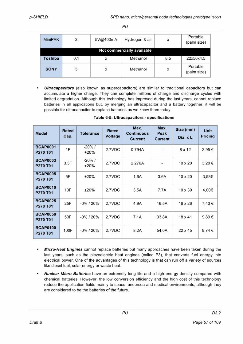
p-SHIELD SPD nano, micro/personal node technologies prototype report
PU
PU D3.2
Draft B Page 57 of 109
MiniPAK 2 5V@400mA Hydrogen & air x Portable (palm size)
Not commercially available
Toshiba 0.1 x Methanol 8.5 22x56x4.5
SONY 3 x Methanol x Portable (palm size)
• Ultracapacitors (also known as supercapacitors) are similar to traditional capacitors but can accumulate a higher charge. They can complete millions of charge and discharge cycles with limited degradation. Although this technology has improved during the last years, cannot replace batteries in all applications but, by merging an ultracapacitor and a battery together, it will be possible for ultracapacitor to replace batteries as we know them today.
Table 6-5: Ultracapacitors - specifications
Model Rated Cap. Tolerance Rated
Voltage
Max. Continuous
Current
Max. Peak
Current
Size (mm)
Dia. x L Unit
Pricing
BCAP0001 P270 T01 1F -20% /
+20% 2.7VDC 0.794A - 8 x 12 2,95 €
BCAP0003 P270 T01 3.3F
-20% / +20% 2.7VDC 2.276A - 10 x 20 3,20 €
BCAP0005 P270 T01 5F ±20% 2.7VDC 1.6A 3.6A 10 x 20 3,58€
BCAP0010 P270 T01 10F ±20% 2.7VDC 3.5A 7.7A 10 x 30 4,00€
BCAP0025 P270 T01 25F -0% / 20% 2.7VDC 4.9A 16.5A 16 x 26 7,43 €
BCAP0050 P270 T01 50F -0% / 20% 2.7VDC 7.1A 33.8A 18 x 41 9,89 €
BCAP0100 P270 T01 100F -0% / 20% 2.7VDC 8.2A 54.0A 22 x 45 9,74 €
• Micro-Heat Engines cannot replace batteries but many approaches have been taken during the last years, such as the piezoelectric heat engines (called P3), that converts fuel energy into electrical power. One of the advantages of this technology is that can run off a variety of sources like diesel fuel, solar energy or waste heat.
• Nuclear Micro Batteries have an extremely long life and a high energy density compared with chemical batteries. However, the low conversion efficiency and the high cost of this technology reduce the application fields mainly to space, undersea and medical environments, although they are considered to be the batteries of the future.

p-SHIELD SPD nano, micro/personal node technologies prototype report
PU
PU D3.2
Draft B Page 58 of 109
6.1.1.1.2 Power harvesting methods
One possibility to overcome power limitations created by the use of batteries as power sources is to get the energy from the environment to either recharge a battery or even, to directly power the electronic device.
Not all technologies are suitable to be integrated in pSHIELD nodes. The scenario is one of the most relevant factors to be considered before selecting the suitable energy harvesting method.
The node with low power consumption is the nano node. A GPS, GSM or GPRS module could be an example about this type of device. The expected power consumption is about 150mW in full operating mode and less than 1mW in sleep mode.
The micro node is more complex than nano node so higher power consumption is expected. A sun spot or a mobile phone could be considered as micro nodes.
In general, these low-efficient technologies are useful only for low energy devices, although the improvements carried out during last years have allowed to increase the application fields.
• Solar power is a clean energy source that needs the sunlight to provide heat and electricity. It is the most popular technology because it could be converted to thermal energy to heat spaces, water or other fluids and it is also possible to get electricity through solar cells or solar power plants. The low efficiency is owing to the irregular sunlight that depends on the location, time of day, time of year and weather conditions. For this reason, a wide area is required to collect the energy at a useful rate.
• Thermal energy converts the waste heat energy variations from the environment (persons, animals, machines, etc.) into electrical energy. The efficiency of this method depends on the difference of temperature between the hot source and the environment. The greater the difference, better the efficiency is.
• Wind power is one of the most old renewable energy sources where the wind is used to generate mechanical power or electricity. Although it is one of the lowest-priced technologies available today, it requires a higher initial investment and may not be a competitive technology if the environment has not a good wind conditions.
• Pressure variations energy comes from atmospheric pressure and/or thermal variations. It should be noted that this method is not widely used because there are not advances implementing large-scale systems.
• Vibrations are present almost everywhere (buildings, transports, industrial environments, etc.) so it is a potential power source. To scavenge power from vibrations, some devices are needed like electromagnetic, electrostatic, and piezoelectric generators that transforms mechanical motion into electricity.
Table 6-6: Power Source – solar energy.
Solar Energy46
Model Rated Power (W)
Capacity (mAh)
Weight (g) Size (mm) Unit
Pricing
Power Curve - - 1200 226.6 152.4x101.6x12.7 $43
46 EarthTech Solar Charges

p-SHIELD SPD nano, micro/personal node technologies prototype report
PU
PU D3.2
Draft B Page 59 of 109
Voltaic Amp Portable Solar Charger
Panel 4 - 480 16.5x14.5x4 $99
Battery 3.3 ([email protected]) 3000 108 102x65x16
Power Monkey Extreme Solar Charger
Panel 1 ([email protected]) - 212 170x91x18 $190
Battery 3.5 ([email protected]) 9000 254 155x62x29
Power Monkey Explorer Solar Charger
Panel 1 ([email protected]) - 82 110x70x10 $101
Battery 3.5 ([email protected]) 2200mA 83 90x45x38
SolarGorilla Solar Charger - 500mAh@20V & 500mAh@5V 680 264.1x198.1x18.8 $220
Table 6-7: Power source – vibrations.
Vibrations47
The harvesters convert unused mechanical vibration into useable electrical energy to power wireless sensor systems. The PMG FSH is designed with highly efficient drive circuitry for charging an external storage device up to 4mA at 5V while reporting power levels via a standard 3-pin IEC connector.
The PMG FSH output can be monitored via the 3-pin IEC interface to provide power output status to a Wireless Sensor Node. The PMG FSH features a high power output up to 20mW.
Table 6-8: Power source – wind power.
Wind Power
Model Rated Power (W)
Start up wind speed (m/s) Size (mm) Unit
Pricing
500 W WindMax Hybrid 485 2.3 800x800x200 (tower)
450€ 60 (diameter)
FlexiEnery400 400 2.5 1500 (diameter) 500€
WS12 650 5.36 1500 (diameter) $570
WG1210C 450 2.24 1300 (diameter) $600
6.1.1.1.3 Power distribution methods
Instead of installing a storage system like a battery or similar, it is possible to distribute power directly to the nodes or even, perform a wirelessly recharging. There are several power distribution methods, although the wired solution is the most well-know as it is the most efficient.
47 http://www.perpetuum.com/fsh.asp

p-SHIELD SPD nano, micro/personal node technologies prototype report
PU
PU D3.2
Draft B Page 60 of 109
There are other less effective methods that are suitable to be installed in those environments where a wired solution is hazardous, inconvenient or impossible. The effectiveness will depend on the relation between the quantity of power absorbed over the one transmitted.
• Electromagnetic Radio Frequency distribution is a radiative wireless power method to transfer electromagnetic energy from a power source to an electrical load. Currently the wireless devices are designed to be periodically recharged. In a near future, all these devices will be powered by energy beacons.
• Elastic or acoustic waves are used to transfer power for actuation, sensing data or other tasks. This technology allows not only power the system but also a full duplex data transmission. Thus it is possible to avoid wirings in those environments where a wired solution it is impossible, like, for instance, in a sealed container.
• Laser beam is a non-radiative technology that can be used for short, mid and long range of transmission. The main reason is that power transmitted by lasers is very much focused so it can be directly transmitted to the receiver with little dispersion loss. The only disadvantage is that relative location of the transmitter and receiver must be precisely known.
6.1.1.2 Monitor Power Consumption
The power protection board could include a current sense amplifier. This solution is not only ideal for all systems where current monitoring is critical but also could be useful for several applications related to battery monitoring, power management, remote sensing or other industrial and embedded applications.
Its output voltage could be monitored to get information about the power consumption at any time. It could be useful to detect an unusual behaviour in the sub-system connected to this output.
6.1.1.3 Power Supply Protections
Both micro and nano nodes, need a protection circuit to avoid problems related to over voltages, overloads, short circuit or over temperatures. Besides, it is important to include a mechanism to plug/unplug critical sections or disconnect any damaged sub-system.
For this proposal, a protection board has been designed. Figure 6-1 shows the schematic with all necessary components to achieve this goal.
Figure 6-1: Protection circuit board – Nano and micro nodes.
• The Fuse is useful to protect the system against excess of current flow caused by an overload or a short circuit. When the current exceeds the rating of the fuse, an excess of heat is produced and the fuse blows out. From that moment on, all the components of the circuit are protected against over current.
• The Thermal Switch is a protection necessary to avoid damages when the system is working out of the defined operating temperature range. It is a thermostat which has an internal contact that will be opened every time the temperature exceeded the limits.
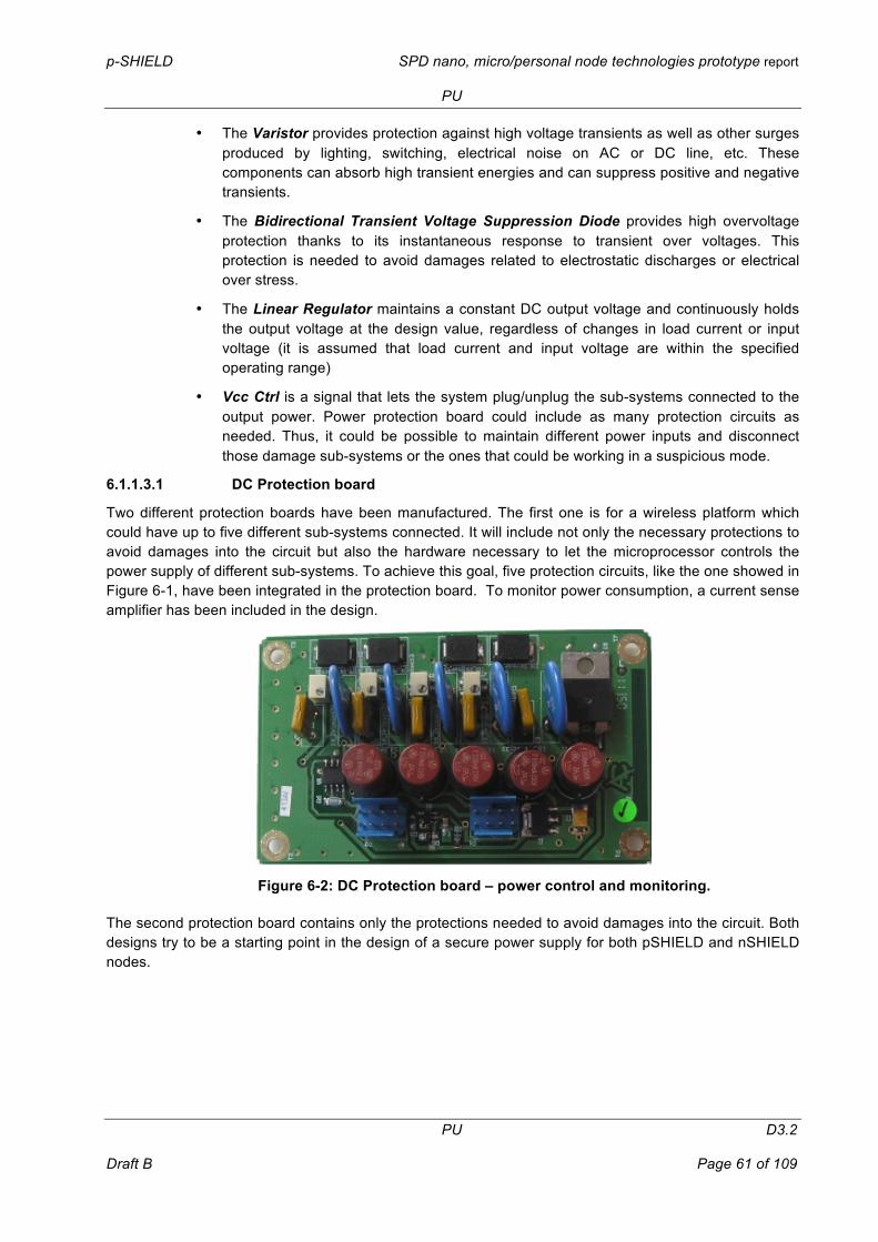
p-SHIELD SPD nano, micro/personal node technologies prototype report
PU
PU D3.2
Draft B Page 61 of 109
• The Varistor provides protection against high voltage transients as well as other surges produced by lighting, switching, electrical noise on AC or DC line, etc. These components can absorb high transient energies and can suppress positive and negative transients.
• The Bidirectional Transient Voltage Suppression Diode provides high overvoltage protection thanks to its instantaneous response to transient over voltages. This protection is needed to avoid damages related to electrostatic discharges or electrical over stress.
• The Linear Regulator maintains a constant DC output voltage and continuously holds the output voltage at the design value, regardless of changes in load current or input voltage (it is assumed that load current and input voltage are within the specified operating range)
• Vcc Ctrl is a signal that lets the system plug/unplug the sub-systems connected to the output power. Power protection board could include as many protection circuits as needed. Thus, it could be possible to maintain different power inputs and disconnect those damage sub-systems or the ones that could be working in a suspicious mode.
6.1.1.3.1 DC Protection board
Two different protection boards have been manufactured. The first one is for a wireless platform which could have up to five different sub-systems connected. It will include not only the necessary protections to avoid damages into the circuit but also the hardware necessary to let the microprocessor controls the power supply of different sub-systems. To achieve this goal, five protection circuits, like the one showed in Figure 6-1, have been integrated in the protection board. To monitor power consumption, a current sense amplifier has been included in the design.
Figure 6-2: DC Protection board – power control and monitoring.
The second protection board contains only the protections needed to avoid damages into the circuit. Both designs try to be a starting point in the design of a secure power supply for both pSHIELD and nSHIELD nodes.

p-SHIELD SPD nano, micro/personal node technologies prototype report
PU
PU D3.2
Draft B Page 62 of 109
Figure 6-3: DC Protection board.
6.1.2 Conclusions
Despite that advances in these technologies have really improved during the last decade, the battery is still the most common and affordable storage system.
In nado nodes, where the size is reduced, the best solution will be the one based on a rechargeable battery (see Figure 6-3) combined with an ultracapacitor (hybrid battery). Thus, the battery lifetime will be extended since the maximum expected power consumption in this kind of nodes is around 150mW (see Table 6-1). An ultracapacitor (see Table 6-5) is useful during transmission/reception operations, where it is expected the maximum power consumption.
Although power consumption of micro nodes is higher, they are slightly bigger than nano nodes (see Table 6-2) so a solution based on a rechargeable battery combined with a solar panel (see Table 6-6) could be considered. If most of the time, these nodes are in low power consumption mode, a method based on harvesting power from vibrations could be implemented (see Table 6-7).
Both protection boards have been tested in order to verify that system is protected against over voltages, overloads, short circuit or over temperatures. Both designs have fulfilled the defined requirements since nodes have integrated not only the necessary protections but also a mechanism to plug-unplug different sub-systems and a sensor to monitor power consumption.

p-SHIELD SPD nano, micro/personal node technologies prototype report
PU
PU D3.2
Draft B Page 63 of 109
7 Elliptic Curve Cryptography for NMP Nodes Elliptic curve cryptography (ECC) is becoming a powerful cryptographic scheme. Because of its efficiency and security is a good alternative to cryptosystems, like RSA and DSA, not just in constrained devices, but also on powerful computers. ECC is very important in the field of low-resource devices such as smart cards and Radio Frequency Identification (RFID) devices because of the significant improvements in terms of speed and memory compared to traditional cryptographic primitives (e.g. RSA). Memory is one of the most expensive resources in the design of embedded systems which encourages the use of ECC on such platforms. Security, implementation and performance of ECC applications on various mobile devices have been examined and it can be concluded that ECC is the most suitable PKC scheme for use in a constrained environment.
More and more electronic transactions for mobile devices are implemented on Internet or wireless networks. In electronic transactions, remote client authentication in insecure channel is an important issue. For example, when one client wants to login a remote server and access its services, such as on-line shopping and pay-TV, both the client and the server must authenticate the identity with each other for the fair transaction. The remote client authentication can be implemented by the traditional public-key cryptography. The computation ability and battery capacity of mobile devices are limited, so traditional PKC, in which the computation of modular exponentiation is needed, cannot be used in mobile devices. Elliptic curve cryptosystem (ECC), compared with other public-key cryptography, has significant advantages like smaller key sizes, faster computations. Thus, ECC-based authentication protocols are more suitable for mobile devices than other cryptosystem. However, like other public-key cryptography, ECC also needs a public key infrastructure (PKI) to maintain the certificates for users’ public keys. When the number of users is increased, PKI needs a large storage space to store users’ public keys and certificates. In addition, users need additional computations to verify the other’s certificate in these protocols.
7.1 Public key infrastructure
A new generation of public key cryptography (PKC) schemes is needed, that has to take into account limitations on power and bandwidth, to provide an adequate level of security for mobile and wireless devices, which use is growing. The Chou`s paper [10] discuss the use of ECC and its security in constrained environments, explores its performance and surveys the use of ECC applications on the market.
The concept of public key cryptography (PKC) was introduced in 1976 by Whitfield Diffie and Martin Hellman. The security of these cryptographic applications is based on hard mathematical problems, namely the integer factorization problem (IFP) and the finite field discrete logarithm problem (DLP). These problems were solved over the years with sub-exponential time algorithms, whose key sizes grew to more than 1000 bits, so as to attain a reasonable level of security. Constrained environments have limited computing power, storage and bandwidth, and carrying out thousand-bit operations becomes an unusable approach to guarantee adequate security. Hand-held devices such as the mobile phones, pagers and PDAs that have very limited processing power and battery life are an example for this problem.
Elliptic curve cryptography (ECC) was proposed by Neal Koblitz and Victor Miller in 1985 and the best known algorithm that solves it runs in full exponential time since the security comes from the elliptic curve logarithm, which is the DLP in a group defined by points on an elliptic curve over a finite field. The key

p-SHIELD SPD nano, micro/personal node technologies prototype report
PU
PU D3.2
Draft B Page 64 of 109
size needed to achieve the same level of security obtainable in conventional PKC schemes results decreased.
7.1.1 ECC Applications
The number of vendors who have incorporated ECC in their products is rising. Even the proponents of traditional cryptographic systems are starting to become more accepting of this promising new technology. An important factor for this emerging trend is the incorporation of ECDSA in several government and major research institution security standards, including IEEE P1363, ANSI X9.62, ISO 11770-3 and ANSI X9.63. ECC is becoming the mainstream cryptographic scheme in all mobile and wireless devices.
ECC applications seen on the market today can be broadly divided into four categories: the Internet, smart cards, PDAs and PCs.
7.1.1.1 Smart cards
The most popular devices for the use of ECC are smart cards. Many manufacturing companies, like Phillips, Fujitsu, MIPS Technologies and DataKey are producing smart cards that use elliptic curve digital signature algorithms. Smart cards are being used in many situations, like bank (credit/debit) cards, electronic tickets and personal identification (or registration) cards since they are very flexible tools.
7.1.1.2 PDAs
PDAs have more computing power compared to most of the other mobile devices, like cell phones or pagers and because of that are very popular for implementing public key cryptosystems. On the other hand they still suffer from limited bandwidth and this makes them an ideal choice for using ECC.
Elliptic curve cryptosystems are a potential match for embedded systems because of their short operand lengths and efficient arithmetic. Because of that Weimerskirch et al. [5] implemented elliptic curves over binary fields on a Palm OS device to investigate if PDAs are sufficient for secure transactions. The most popular PDAs use the Palm Operating System (Palm OS). They used a Handspring Visor model with 2 MB of memory. This device has a Motorola Dragonball CPU that provides eight data registers and seven address registers, all of them 32-bit in size. The processor offers 16-bit and 32-bit operations and runs at 16 MHz. They chose the NIST recommended random and Koblitz curves over GF(2163) and selected binary curves since the integer multiplication unit of the Dragonball processor is very slow. Koblitz curves allow shorter run times while they provide nearly the same level of security according to current knowledge about attacks.
It results that a normal transaction such as a key exchange or signature verification can be done in less than 2.4 seconds while signature generation can be done in less than 0.9 seconds. Koblitz curves are particular suitable for these devices since they allow running times that will probably be tolerated by most users.
ECC is becoming a powerful cryptographic scheme. Because of its efficiency and security is a good alternative to cryptosystems, like RSA and DSA, not just in constrained devices, but also on powerful computers. Security, implementation and performance of ECC applications on various mobile devices have been examined and it can be concluded that ECC is the most suitable PKC scheme for use in a constrained environment.
7.2 Signature schemes
The blind signature scheme is a protocol for obtaining a signature from a signer, but the signer can neither learn the messages nor see the signatures the recipients obtain afterwards. In proxy signature

p-SHIELD SPD nano, micro/personal node technologies prototype report
PU
PU D3.2
Draft B Page 65 of 109
scheme, the original signer delegates his signing capacity to a proxy signer who can sign a message submitted on behalf of the original signer. A verifier can validate its correctness and can distinguish between a normal signature and a proxy signature. In multi-proxy signature scheme, an original signer is allowed to authorize a group of proxy members to generate the multi signature on behalf of the original signer.
7.2.1 Proxy blind signature scheme
A proxy blind signature scheme is a digital signature scheme that ensures the properties of proxy signature and blind signature. In a proxy blind signature, an original signer delegates his signing capacity to proxy signer. A proxy blind signature scheme is a special form of blind signature which allows a designated person called proxy signer to sign on behalf of two or more original signers without knowing the content of the message or document. It combines the advantages of proxy signature, blind signature and multi-signature.
A proxy blind signature scheme consists of the following three phases:
• Proxy key generation • Proxy blind multi-signature scheme • Signature verification
Most of the proxy blind signature schemes were developed based on the mathematical hard problems integer factorization (IFP) and simple discrete logarithm (DLP) which take sub-exponential time to solve. Alghazzawi et al. [7] describe a simple proxy blind signature scheme based on Elliptic Curve Discrete Logarithm Problem (ECDLP), which is solved in fully-exponential time. The algorithms for solving the ECDLP become infeasible much more rapidly as the problem size increases more than those algorithms for the IFP and DLP. Thus, ECC offers security equivalent to RSA and DSA while using far smaller key sizes. The benefits of this higher-strength per-bit include higher speeds, lower power consumption, bandwidth savings, storage efficiencies, and smaller certificates. This can be implemented in low power and small processor mobile devices such as smart card, PDA etc. which work in low power and small processor.
7.2.1.1 Proposed Protocol
The protocol involves three entities:
• Original signer S, • Proxy signer s P and • Verifier V.
It is described as follows.
7.2.1.1.1 Proxy Phase
• Proxy generation:
The original signer S selects random integer k in the interval [1, 𝑛 − 1]. Computes 𝑅 = 𝑘𝑃 = (𝑥!, 𝑦!) and 𝑟 = 𝑥!𝑚𝑜𝑑 𝑛. Where 𝑥! is regarded as an integer between 0 and q–1, then computes 𝑠 = (𝑑 + 𝑘 ∗𝑟) 𝑚𝑜𝑑 𝑛 and computes 𝑄! = 𝑠𝑃.
• Proxy delivery:
The original signer S sends (𝑠, 𝑟) to the proxy signer 𝑃! and make 𝑄! public.
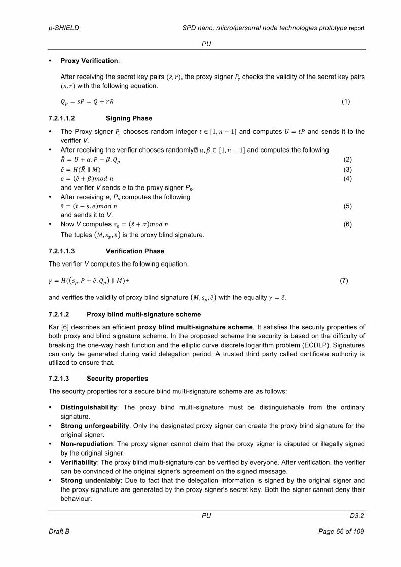
p-SHIELD SPD nano, micro/personal node technologies prototype report
PU
PU D3.2
Draft B Page 66 of 109
• Proxy Verification:
After receiving the secret key pairs (𝑠, 𝑟), the proxy signer 𝑃! checks the validity of the secret key pairs (𝑠, 𝑟) with the following equation.
𝑄! = 𝑠𝑃 = 𝑄 + 𝑟𝑅 (1)
7.2.1.1.2 Signing Phase
• The Proxy signer 𝑃! chooses random integer 𝑡 ∈ [1, 𝑛 − 1] and computes 𝑈 = 𝑡𝑃 and sends it to the verifier V.
• After receiving the verifier chooses randomly� 𝛼,𝛽 ∈ [1, 𝑛 − 1] and computes the following 𝑅 = 𝑈 + 𝛼.𝑃 − 𝛽.𝑄! (2) 𝑒 = 𝐻(𝑅 ∥ 𝑀) (3) 𝑒 = 𝑒 + 𝛽 𝑚𝑜𝑑 𝑛 (4) and verifier V sends e to the proxy signer Ps.
• After receiving e, Ps computes the following 𝑠 = 𝑡 − 𝑠. 𝑒 𝑚𝑜𝑑 𝑛 (5) and sends it to V.
• Now V computes 𝑠! = 𝑠 + 𝛼 𝑚𝑜𝑑 𝑛 (6) The tuples 𝑀, 𝑠!, 𝑒 is the proxy blind signature.
7.2.1.1.3 Verification Phase
The verifier V computes the following equation.
𝛾 = 𝐻( 𝑠!.𝑃 + 𝑒.𝑄! ∥ 𝑀)+ (7)
and verifies the validity of proxy blind signature 𝑀, 𝑠!, 𝑒 with the equality 𝛾 = 𝑒.
7.2.1.2 Proxy blind multi-signature scheme
Kar [6] describes an efficient proxy blind multi-signature scheme. It satisfies the security properties of both proxy and blind signature scheme. In the proposed scheme the security is based on the difficulty of breaking the one-way hash function and the elliptic curve discrete logarithm problem (ECDLP). Signatures can only be generated during valid delegation period. A trusted third party called certificate authority is utilized to ensure that.
7.2.1.3 Security properties
The security properties for a secure blind multi-signature scheme are as follows:
• Distinguishability: The proxy blind multi-signature must be distinguishable from the ordinary signature.
• Strong unforgeability: Only the designated proxy signer can create the proxy blind signature for the original signer.
• Non-repudiation: The proxy signer cannot claim that the proxy signer is disputed or illegally signed by the original signer.
• Verifiability: The proxy blind multi-signature can be verified by everyone. After verification, the verifier can be convinced of the original signer's agreement on the signed message.
• Strong undeniably: Due to fact that the delegation information is signed by the original signer and the proxy signature are generated by the proxy signer's secret key. Both the signer cannot deny their behaviour.

p-SHIELD SPD nano, micro/personal node technologies prototype report
PU
PU D3.2
Draft B Page 67 of 109
• Unlinkability: When the signer is revealed, the proxy signer cannot identify the association between the message and the blind signature he generated.
• Secret key dependencies: Proxy key or delegation pair can be computed only by the original signer's secret key.
• Prevention of misuse: The proxy signer cannot use the proxy secret key for purposes other than generating valid proxy signatures. In case of misuse, the responsibility of the proxy signer should be determined explicitly.
7.3 ECC in software trusted platform module
Trusted computing discussed earlier is an emerging concept that deals with information security concerns in a wide variety of computing systems. Trusted computing standards are driven by the computing and communications industries through the Trusted Computing Group (TCG). Hardware and software improvements to the target system are required for the usual approach to trusted computing, including the addition of a separate chip called the TPM that is attached to the target system.
The TPM provides capabilities for secure storage; secure reporting of platform configuration measurements, and cryptographic key generation. In addition the TPM chip implements tamper-resistance techniques to prevent a wide range of physical and hardware-based attacks.
Trusted computing has applicability to a wide range of embedded systems. Recent efforts to adapt trusted computing standards to resource-constrained environments include the TCG’s Mobile Phone Working Group and the Trusted Mobile Platform Alliance. The hardware enhancements, including the addition of the TPM chip, may impose an overhead in the context of cost and size in resource-constrained embedded systems and this is not acceptable. For such systems, one option is to use a software-based TPM (SW-TPM), which implements TPM functions using software that performs in a protected execution domain on the embedded processor itself in order to enable the adoption of trusted computing techniques. It is also important to ensure that the computational and energy requirements for SW-TPMs are acceptable since many embedded systems have limited processing capabilities and are battery-powered.
In terms of protection against physical and hardware attacks SW-TPM is not completely equivalent to a conventional TPM chip. SW-TPM can be executed within protected or isolated execution domains that are provided by embedded CPUs (e.g., ARM TrustZone), and can utilize on-chip storage in order to provide a reasonable degree of tamper-resistance. The question that arises is whether the computational and energy requirements to perform the TPM functions are acceptable.
In the article of Aaraj et al. [1], [2] is performed an evaluation of the energy and execution time overheads for a SW-TPM implementation on a handheld appliance (Sharp Zaurus PDA). The execution time and energy required by each TPM command through actual measurements on the target platform is characterized. It is shown that for most commands, overheads are primarily due to the use of 2,048-bit RSA operations that are performed within the SW-TPM. They replace the RSA algorithm with the Elliptic Curve Cryptography (ECC) specified in the Trusted Computing Group (TCG) standards, in order to alleviate SW-TPM overheads. They also evaluate the overheads of using the SW-TPM in the context of various end applications, including trusted boot of the Linux operating system (OS), a secure VoIP client, and a secure Web browser. Their experiments indicate that this optimization can significantly reduce SW-TPM overheads (an average of 6.51X execution time reduction and 6.75X energy consumption reduction for individual TPM commands, and an average of 10.25X execution time reduction and 10.75X energy consumption reduction for applications). This work demonstrates that ECC-based SW-TPMs are a viable approach to realizing the benefits of trusted computing in resource-constrained embedded systems.

p-SHIELD SPD nano, micro/personal node technologies prototype report
PU
PU D3.2
Draft B Page 68 of 109
This work contributes in the following way:
• A comprehensive characterization of SW-TPM running on a battery-powered handheld device (Sharp Zaurus PDA) is performed, and the execution time and energy requirements for various TPM commands are measured.
• The overheads imposed by using TPM functions in end applications are evaluated, including trusted boot of the Linux OS, secure file storage utility, secure VoIP client, and secure web browser.
• In order to alleviate the overheads imposed by SW-TPM, it is proposed and evaluated the use of ECC as a replacement for the RSA algorithm specified in the TCG standards. The experiments indicate that results in a substantial reduction in SW-TPM overheads.
This work demonstrates the feasibility of using SW-TPM to realize the benefits of trusted computing in resource-constrained embedded systems.
7.3.1 SW-TPM Implementation
The TPM security features are very useful in many embedded systems. Some embedded systems cannot be augmented with a conventional TPM chip because of the area and cost constraints. Here, the feasibility of a SW-TPM is explored, which performs the same functions as a hardware TPM, i.e., supports all the three roots of trust, as well as other cryptographic capabilities. SW-TPM does not provide the same security level as a TPM chip. Executing the SW-TPM in a protected execution domain of the CPU (e.g., ARM Trust-Zone), and using on-chip memory, provides resistance to software attacks, including compromises of the OS, and a limited number of physical attacks.
The implementation of SW-TPM is adapted from the public domain TPM emulator [3], which provides basic TPM functions, such as RSA cryptography and HMAC and SHA-1 hashing functions, and provides several TPM commands.
The emulator has been changed as follows:
• Random number generation: A hash-complemented Mersenne Twister (MT) random number generator [4] is used, i.e., we run the output of MT through SHA-1.
• ECC: SW-TPM supports ECC in the binary field GF(2m). ECC on this embedded platform is used because of its small key sizes compared to RSA for offering the same security robustness. Hence, it requires less resources such as processor cycles and energy. ECC-enabled SW-TPM supports key generation and validation, digital signature generation and verification, encryption, and decryption. Supported ECC key sizes are 224 bits (equivalent to 2048-bit RSA keys), 192 bits (not equivalent to RSA key), and 160 bits (equivalent to 1024-bit RSA keys).
• AES_CBC cryptography: SW-TPM supports the Advanced Encryption Standard (AES) algorithm, running in Cipher Block Chaining (CBC) mode. This engine is specifically used for ECC encryption and decryption, and for decrypting AIK credentials.
7.3.2 Measurement results
The execution time and energy consumed by SW-TPM on the PDA is presented here in order to execute various TPM commands. The presented results are for the original RSA-based SW-TPM and for the proposed ECC-based SW-TPM.
For commands categorized as the storage and key management commands, and TPM_Sign, measurements are performed for different key sizes. For commands that process user data, the data size is varied. The results of these experiments are reported in Table 7-1. The command executed is presented in Column 1. Columns 2-3 give the key size (K) and data size (D). For commands that do not involve cryptographic operations K (D) is indicated as N/A. Column 4 gives energy measurements in milliJoules (mJ), and column 5 reports the execution times for the TPM commands in milliseconds
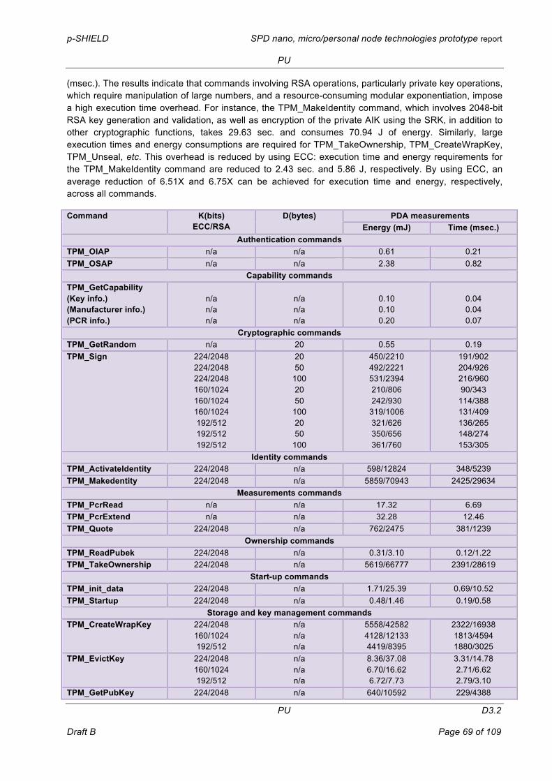
p-SHIELD SPD nano, micro/personal node technologies prototype report
PU
PU D3.2
Draft B Page 69 of 109
(msec.). The results indicate that commands involving RSA operations, particularly private key operations, which require manipulation of large numbers, and a resource-consuming modular exponentiation, impose a high execution time overhead. For instance, the TPM_MakeIdentity command, which involves 2048-bit RSA key generation and validation, as well as encryption of the private AIK using the SRK, in addition to other cryptographic functions, takes 29.63 sec. and consumes 70.94 J of energy. Similarly, large execution times and energy consumptions are required for TPM_TakeOwnership, TPM_CreateWrapKey, TPM_Unseal, etc. This overhead is reduced by using ECC: execution time and energy requirements for the TPM_MakeIdentity command are reduced to 2.43 sec. and 5.86 J, respectively. By using ECC, an average reduction of 6.51X and 6.75X can be achieved for execution time and energy, respectively, across all commands.
Command K(bits) ECC/RSA
D(bytes) PDA measurements Energy (mJ) Time (msec.)
Authentication commands TPM_OIAP n/a n/a 0.61 0.21 TPM_OSAP n/a n/a 2.38 0.82
Capability commands TPM_GetCapability (Key info.) (Manufacturer info.) (PCR info.)
n/a n/a n/a
n/a n/a n/a
0.10 0.10 0.20
0.04 0.04 0.07
Cryptographic commands TPM_GetRandom n/a 20 0.55 0.19 TPM_Sign 224/2048
224/2048 224/2048 160/1024 160/1024 160/1024 192/512 192/512 192/512
20 50
100 20 50
100 20 50
100
450/2210 492/2221 531/2394 210/806 242/930
319/1006 321/626 350/656 361/760
191/902 204/926 216/960 90/343
114/388 131/409 136/265 148/274 153/305
Identity commands TPM_ActivateIdentity 224/2048 n/a 598/12824 348/5239 TPM_Makedentity 224/2048 n/a 5859/70943 2425/29634
Measurements commands TPM_PcrRead n/a n/a 17.32 6.69 TPM_PcrExtend n/a n/a 32.28 12.46 TPM_Quote 224/2048 n/a 762/2475 381/1239
Ownership commands TPM_ReadPubek 224/2048 n/a 0.31/3.10 0.12/1.22 TPM_TakeOwnership 224/2048 n/a 5619/66777 2391/28619
Start-up commands TPM_init_data 224/2048 n/a 1.71/25.39 0.69/10.52 TPM_Startup 224/2048 n/a 0.48/1.46 0.19/0.58
Storage and key management commands TPM_CreateWrapKey 224/2048
160/1024 192/512
n/a n/a n/a
5558/42582 4128/12133 4419/8395
2322/16938 1813/4594 1880/3025
TPM_EvictKey 224/2048 160/1024 192/512
n/a n/a n/a
8.36/37.08 6.70/16.62 6.72/7.73
3.31/14.78 2.71/6.62 2.79/3.10
TPM_GetPubKey 224/2048 n/a 640/10592 229/4388

p-SHIELD SPD nano, micro/personal node technologies prototype report
PU
PU D3.2
Draft B Page 70 of 109
160/1024 192/512
n/a n/a
471/1504 516/852
157/567 172/453
TPM_LoadKey 224/2048 160/1024 192/512
n/a n/a n/a
810/14547 593/4557 737/2092
336/5367 261/1796 301/841
TPM_Seal 224/2048 224/2048 224/2048 160/1024 160/1024 160/1024 192/512 192/512 192/512
20 50
100 20 50
100 20 50
100
1103/3751 1125/3785 1313/4271 769/1898 806/2195 819/2965
1001/1019 1026/1063 1093/1326
463/1476 472/1564 530/1761 322/796 334/967
342/1178 420/427 431/481 444/551
TPM_Unseal 224/2048 160/1024 192/512
256 256 256
1444/14056 952/4679
1279/1778
585/5520 391/1880 525/714
TPM_Unbind 224/2048 160/1024 192/512
256 256 256
1459/10480 974/4269
1284/1616
576/4103 384/1699 524/699
Table 7-1: Energy and execution time for TPM commands
Macromodels that capture the energy for the commands TPM_Sign and TPM_Seal as a function of the key size K and data size D are presented in the Table 7-2. Values of K are up to 2048 (224) bits for RSA (ECC), and D assumes values up to 144 Bytes. From the macromodels, and the numbers reported in Table 7-1 can be concluded that energy and execution time requirements vary more considerably with the key size rather than with the data size (especially with RSA cryptography).
Command Crypto type Energy model (C + A*D + B*D2 + X*K + Y*K2 (mJ))
TPM_Sign ECC
RSA
31.269 + 1.434*D – 0.004*D2 + 0.642*K + 0.011*K2
29.994 + 10.389*D – 0.061*D2 + 0.349*K + 0.00029*K2
TPM_Seal ECC
RSA
6.415 + 0.067*D – 0.012*D2 + 3.980*K + 0.005*K2
5.766 + 10.033*D – 0.142*D2 + 2.435*K + 0.00026*K2
Table 7-2: Energy macromodels for the TPM_Sign and TPM_Seal.
The presented results are based on the average of several executions (16) of each command, in order to account for uncontrollable variables, such as the randomness of the keys, and to minimize measurement error for commands that require small running times.
It is also important to place the overheads in the context of actual applications not only for evaluating the requirements of SW-TPM in isolation. Trusted extensions for several applications are proposed and the impact of using SW-TPM on their execution time and energy consumption is studied.
7.3.3 User applications with SW-TPM
In the paper [1] is presented an experiment where SW-TPM was used in the context of four different applications. The trusted extensions of four applications (Trusted Boot, Secure Storage, Secure Voice over Internet Protocol (VoIP), and Secure Web Browsing) are described and the effect of these
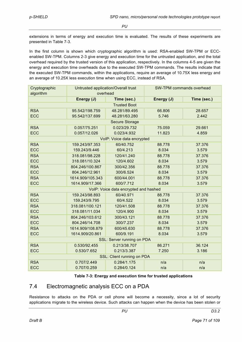
p-SHIELD SPD nano, micro/personal node technologies prototype report
PU
PU D3.2
Draft B Page 71 of 109
extensions in terms of energy and execution time is evaluated. The results of these experiments are presented in Table 7-3.
In the first column is shown which cryptographic algorithm is used: RSA-enabled SW-TPM or ECC-enabled SW-TPM. Columns 2-3 give energy and execution time for the untrusted application, and the total overhead required by the trusted version of this application, respectively. In the columns 4-5 are given the energy and execution time overheads due to the executed SW-TPM commands. The results indicate that the executed SW-TPM commands, within the applications, require an average of 10.75X less energy and an average of 10.25X less execution time when using ECC, instead of RSA.
Cryptographic algorithm
Untrusted application/Overall trust overhead
SW-TPM commands overhead
Energy (J) Time (sec.) Energy (J) Time (sec.) Trusted Boot
RSA ECC
95.542/198.759 95.542/137.699
48.281/89.495 48.281/63.280
66.806 5.746
28.657 2.442
Secure Storage RSA ECC
0.057/75.251 0.057/12.026
0.023/29.732 0.023/4.932
75.059 11.823
29.661 4.859
VoIP: Voice data encrypted RSA ECC
159.243/97.353 159.243/9.446
60/40.752 60/4.213
88.778 8.034
37.376 3.579
RSA ECC
318.081/98.228 318.081/10.324
120/41.240 120/4.602
88.778 8.034
37.376 3.579
RSA ECC
804.246/100.867 804.246/12.961
300/42.356 300/6.524
88.778 8.034
37.376 3.579
RSA ECC
1614.909/105.343 1614.909/17.366
600/44.001 600/7.712
88.778 8.034
37.376 3.579
VoIP: Voice data encrypted and hashed RSA ECC
159.243/98.893 159.243/9.795
60/40.971 60/4.522
88.778 8.034
37.376 3.579
RSA ECC
318.081/100.121 318.081/11.034
120/41.508 120/4.900
88.778 8.034
37.376 3.579
RSA ECC
804.246/103.612 804.246/14.708
300/43.121 300/7.237
88.778 8.034
37.376 3.579
RSA ECC
1614.909/108.879 1614.909/20.861
600/45.630 600/9.191
88.778 8.034
37.376 3.579
SSL: Server running on PDA RSA ECC
0.530/92.455 0.530/7.652
0.213/38.707 0.213/3.387
86.271 7.250
36.124 3.186
SSL: Client running on PDA RSA ECC
0.707/2.449 0.707/0.259
0.284/1.175 0.284/0.124
n/a n/a
n/a n/a
Table 7-3: Energy and execution time for trusted applications
7.4 Electromagnetic analysis ECC on a PDA
Resistance to attacks on the PDA or cell phone will become a necessity, since a lot of security applications migrate to the wireless device. Such attacks can happen when the device has been stolen or

p-SHIELD SPD nano, micro/personal node technologies prototype report
PU
PU D3.2
Draft B Page 72 of 109
lost and also during everyday use when unintentional electromagnetic (EM) waves radiated from the wireless device during cryptographic computations may reveal confidential data to an attacker. For example an attacker may successfully attack confidential memory in a wireless device obtaining the secret keys stored in there. This attack may be possible through loss or theft of the device. Alternatively the attack can happen also through temporary access to the device by monitoring the EM waves deriving from the device while performing cryptographic computations. In that case the attacker may be able to extract the encryption keys and making future wireless communications insecure. For wireless embedded systems large overheads in energy to achieve resistance to attacks are not practical. Beside smartcard research few researchers have examined secure implementations of cryptographic software (Rijndael [17]) under the threat of EM attacks on 32-bit processors. The cryptographic algorithms which are essential for these applications are typically run by embedded processors in these wireless devices but it is known that they consume a lot of energy. These attack resistant algorithms have been developed for smartcard applications, where energy dissipation is not such important. There is an important need to study EM attacks and energy optimised countermeasures on wireless portable devices, such as PDAs, cell phones, etc.
Thus, although many wireless portable devices offer more resistance to bus probing and power analysis attacks due to their compact size, susceptibility to electromagnetic (EM) attacks must be analyzed. Paper from Gebotys et al. [8] presents a real EM-based attack of a PDA running elliptic curve cryptography and a new frequency-based differential EM analysis, which computes the power spectral density and spectrogram. Unlike previous research the new differential analysis does not require perfect alignment of EM traces, thus supporting attacks on real embedded systems.
7.4.1 Differential analysis in the frequency domain
Gebotys et al. [8] proposed a performing analysis in the frequency domain, which is an extension of the existing differential side channel attack, where analysis is performed in the time domain. Here are presented two approaches:
• differential frequency analysis (DFA), where the power spectral density (PSD) is used for analysis, • differential spectrogram analysis (DSA), since a spectrogram is created.
The problem of misalignment (or time-shifts) in traces is solved by analyzing signals captured in the frequency domain since fast Fourier transform (FFT) analysis is time-shift invariant.
Both the DFA and DSA are important for attacking real embedded systems where uncorrelated temporal misalignment (or time shifting) of traces is a big concern. Some structures cannot be revealed with time domain analysis. Contrary to that frequency analysis may reveal loops and other repeating structures in an algorithm. There are two problems with using frequency domain signals in differential analysis:
• It reveals no information of when data-dependant operations occur. This timing information is very useful as it helps an adversary focus the signal analysis on these data dependant operations.
• Any peaks in frequency domain due to an event that occurs in a short duration can be visible if the acquisition duration is a lot longer. The solution of these problems is to use spectrogram, which is a time dependant frequency analysis.
The attack of an elliptic curve algorithm presented here uses EM traces. Only when the 1st and 2nd most significant bits of the elliptic point data are used for partitioning, both the DEMA (differential EM analysis) and DSA (differential spectrogram analysis) attacks are successful on the elliptic curve algorithm. This attack works if the MSB’s (most significant bit) are correlated with EM activity from the overflow or underflow computations. Using the same algorithm for finite field computations regardless of whether an overflow occurs or not can be a possible countermeasure for the MSB differential analysis attack of ECC.

p-SHIELD SPD nano, micro/personal node technologies prototype report
PU
PU D3.2
Draft B Page 73 of 109
The analysis techniques proposed here successfully obtain the correct key from elliptic curve cryptography. They are general and applicable to other cryptographic algorithms, power as well as EM, and other embedded systems. A new frequency-based (time-shift invariant) differential analysis is presented using real EM measurements from a PDA device executing Java-based cryptography. Previous differential analysis techniques, which required alignment of traces in the time domain, were not successful in correlating EM signals to bits of the data. This research supports low energy security for embedded systems which will be prevalent in wireless embedded devices of the future.
7.5 ECC in wireless sensors
A WSN is a wireless ad-hoc network consisting of resource-constrained sensoring devices (limited energy source, low communication bandwidth, small computational power) and one or more base stations. The base stations are more powerful and collect the data gathered by the sensor nodes so it can be analyzed. Routing is accomplished by the nodes themselves as any ad hoc network through hop-by-hop forwarding of data. Common WSN applications range from battlefield exploration and emergency rescue operations to surveillance and environmental protection.
Security and cryptography on WSNs meet several open problems even though several years of intense research. Given the limited computational power and the resource-constrained nature of the sensoring devices, the deployment of cryptography in sensor networks is a difficult task. Aranha et al. `s paper [12] presents the implementation of elliptic curve cryptography in the MICAz Mote, a sensor platform to develop optimizations specifically:
(i) the cost of memory addressing; (ii) the cost of memory instructions; (iii) the limited flexibility of bitwise shift instructions.
This work presents efficient implementations for arithmetic of binary field algorithms such as squaring, multiplication, modular reduction and inversion at two different security levels. These implementations take into account the characteristics of the target platform. The implementation of field multiplication and modular reduction algorithms focuses on the reduction of memory accesses and appears as the fastest result for this platform.
Finite field arithmetic was implemented in C and Assembly and elliptic curve arithmetic was implemented in Koblitz and generic binary curves. Here are obtained the fastest binary field arithmetic implementations in C and Assembly published for the target platform. Significant performance benefits where achieved by the Assembly implementation, resulting from fine-grained resource allocation and instruction selection. The performance of implementations is illustrated with timings for key agreement and digital signature protocols. Results strongly indicate that binary curves are the most efficient alternative for the implementation of elliptic curve cryptography in this platform.
Optimizations produced a point multiplication at the 160-bit security level under 1/3 of a second, an improvement of 72% compared to the best implementation of a Koblitz curve previously published and an improvement of 61% compared to the best implementation of binary curves. When compared to the best implementation of prime curves, is obtained a performance gain of 57%.
7.6 Improvements in ECC for resource-constrained devices
Elliptic curve cryptography (ECC) is very important in the field of low-resource devices such as smart cards and Radio Frequency Identification (RFID) devices because of the significant improvements in terms of speed and memory compared to traditional cryptographic primitives (e.g. RSA). Memory is one of

p-SHIELD SPD nano, micro/personal node technologies prototype report
PU
PU D3.2
Draft B Page 74 of 109
the most expensive resources in the design of embedded systems which encourages the use of ECC on such platforms.
Scalar multiplication in ECC implementation is the operation used in many cryptographic primitives for solving the elliptic curve discrete logarithm problem (ECDLP), i.e. finding the discrete logarithm for Q with respect to the elliptic curve point P. It is a process where a secret scalar k is multiplied with a point P on an elliptic curve E(Fq) getting in the point Q and is the most resource-consuming operation.
In embedded systems memory and computational power are scarce resources. In that case, the scalar multiplication can be improved with a method called Montgomery ladder [13]. In this process the y-coordinate of the involved elliptic curve points can be omitted, which lowers the memory requirements for low-resource designs. In addition, it implicitly provides resistance against certain implementation attacks which encourages its use in security-related applications. Meloni [14] proposed another improvement where he showed that points on an elliptic curve can be added quickly when they share a common coordinate, e.g. the projective Z-coordinate. He applied the formula to specific Euclid addition chains to perform a scalar multiplication which improves the speed of ECC implementations and reduces the memory requirements by one coordinate. The proposal of Meloni was extended by Goundar [15] who provided a formula over prime fields that can be applied to classical binary scalar multiplication methods. He introduced a new operation (conjugate co-Z addition) that can be used together with the addition formula of Meloni to perform fast computations with points sharing the same Z-coordinate (co-Z arithmetic).
Performance of scalar multiplication in elliptic curve cryptography implementations can be improved by sharing a common coordinate. Hutter [11] presented a new formula for elliptic curves over prime fields that provide efficient (speed-wise and memory-wise) point addition and doubling using the Montgomery ladder especially applicable to resource-constrained devices. The proposed formula uses out-of-place operations to insure that no additional memory for any implementation of the underlying finite-field operations is required and all computations are performed in a common projective Z-coordinate representation to reduce the memory requirements of low-resource implementations. In terms of memory and speed the results outperform existing solutions and allow a fast and secure implementation suitable for low-resource devices and embedded systems.
The new formula for elliptic curves over finite fields of characteristic q ≠ 2, 3 apply the co-Z method to the Montgomery ladder scalar multiplication. The given formula perform a differential addition-and-doubling operation of elliptic curve points using x-coordinates only, i.e. two projective X-coordinates of the involved points and a common Z-coordinate. The formula leads to very efficient scalar multiplications especially suitable to low-resource devices. The practical constraint imposed by the implementations of both the modular multiplication and the modular squaring is considered, which may not support the result to be written in-place, which is overwriting one of the operands. This constraint allows saving memory with many efficient implementations of those. Unfortunately this typically implies the need of more memory than claimed in order to implement formula which have been designed with in-place operations. The formula can be applied on general elliptic curves and allow the integration of conventional countermeasures against implementation attacks. They can be efficiently applied in low-resource implementations of RFIDs, smart cards, and other embedded systems.
7.6.1 Key agreement protocol for mobile devices on elliptic curve cryptosystem
A cross-realm client-to-client password-authenticated key agreement (CR-C2C-PAKA) protocol is designed to solve the problem of secure client-to-client communication. It provides a method to achieve authenticated key agreement in a cross-realm setting for clients, who registered in cross realms (servers) with different passwords.

p-SHIELD SPD nano, micro/personal node technologies prototype report
PU
PU D3.2
Draft B Page 75 of 109
Secure client-to-client communications are required urgently in various areas, such as wireless networks, peer-to-peer networks, client-to-client E-commerce and so on, since the development of the electronic and network technologies is fast. For example, in a wireless network communication environment, a secure peer-to-peer channel, between a client Alice registered in one server SA and another client Bob registered in a different server SB, may be a primary concern over an insecure and public channel. Nowadays, electronic commerce are more popular and convenient, client-to-client businesses are also more and more prevalent day by day and mobile intelligent devices, such as cell phones, PDAs, notebook PCs and so on, are everywhere. Then arise the question, how to design such a CR-C2C-PAKA protocol, which can be implemented using mobile intelligent devices.
Cross-realm client-to-client password-authenticated key agreement protocol was first proposed by Byun et al. [18] in 2002. A lot of researchers worked on these protocols from then, presented many attacks to show that the previous protocols were not secure and improved protocols to enhance the security. The first provably secure C2CPAKE protocol was introduced by Byun et al. [19] in 2007. Later in 2009 was shown by Feng et al. [20] that the existing protocols designed in secret key setting were not secure against password-compromise impersonation and proposed an improved protocol based on the public key cryptosystem with digital signature system which was proved secure to resist all known attacks, such as off-line password dictionary attack, Denning-Sacco attack, replay attack, one-way man-in-the-middle attack and password-compromise impersonation attack. The secure CR-C2C-PAKA protocol based on smart cards in secret-key setting with modified formal security proof was proposed lately by Jin et al. [21]. The smart cards are high cost and the auxiliary infrastructures and related standards of interfaces are lacking. Because of that such protocols were not widely implemented except in special areas. In 2009, Rhee et al. [22] proposed an improved scheme to enhance the security flaws of Khan-Zhang’s scheme [23], which was vulnerable to user impersonation attack without using smart cards. Yang et al. [24] recently introduced elliptic curve cryptosystem into an ID-based remote user mutual authentication with key agreement scheme for mobile devices.
A new improved cross-realm client-to-client password-authenticated key agreement protocol based on elliptic curve cryptosystem for mobile devices is presented in the paper [9]. The proposed protocol is more secure, efficient, convenient, flexible and practical in our daily life. It can be implemented in secret-key (symmetric) setting with the resistance of known attacks including password-compromise impersonation attack. In order to augment the security flaws and increase the efficiency of computation with shorter key size elliptic curve cryptosystem is introduced into this protocol. Compared with the protocols based on smart cards or public key cryptosystems, the new protocol is designed for mobile devices, which are prevalent and convenient than smart cards or public cryptosystems in our daily life. The security of the protocol bases upon elliptic curve discrete logarithm problem. The risky password (verifier) tables or expensive auxiliary equipments are not required in this protocol. Rhee et al.’s remote authentication scheme [25] using elliptic curve cryptosystem is also improved and applied to the presented cross-realm client-to-client password-based authenticated key agreement protocol. Moreover, two additional functions are provided for users and servers, called secrets update phase and revocation phase for security and flexibility. At last, the security analysis shows that the protocol is secure against known common attacks, including the password compromise impersonation attack in the secret-key setting.
7.7 Comparison: ECC vs. Others Alternative Cryptography for Resource-Constrained Devices
At the same security level the NTRUEncrypt convolution operations with binary polynomials are 7,5 - 15 times faster, and NTRUEncrypt convolutions with product-form polynomials are 15 - 30 times faster than ECC point multiplications. For encryption, ECC requires an additional point multiplication to a known base point, which increases encryption times by a factor of 1,3 - 2. For decryption, NTRUEncrypt-NAEP

p-SHIELD SPD nano, micro/personal node technologies prototype report
PU
PU D3.2
Draft B Page 76 of 109
requires an additional encryption operation for the consistency, increasing decryption times by a factor of 2. [26].
Cryptographic algorithm
Properties Weakness
ECC • The smaller ECC keys it turn makes the cryptographic operations that must be performed by the communicating devices to be embedded into considerably smaller hardware, so that software applications may complete cryptographic operations with fewer processor cycles, and operations can be performed much faster, while still retaining equivalent security. This means reduced power consumption, less space consumed on the printed circuit board, and software applications that run more rapidly make lower memory demands. For communication using smaller devices and asymmetric cryptosystem ECC is used.
• High security for relatively small key sizes. • Smaller key sizes, faster computations compared with
other public-key cryptography • Reduce energy consumption and to prolong life time of
sensor nodes • More suitable for mobile devices than other
cryptosystem. • To solve the problems, several ID-based authentication
protocols on ECC are proposed. • Faster execution timings for the schemes, which is
beneficial to systems where real time performance is a critical factor.
• In RSA cryptosystem, the security increases sub exponentially whereas in elliptic curve cryptosystem, the security increases directly exponentially. The consequence is smaller key sizes, bandwidth savings, and faster implementations features which are especially attractive for security applications where computational power and integrated circuit space is limited, such as smart cards, PC (personal computer) cards, and wireless devices.
• ECC is more appropriate for resource-constrained devices compare to RSA.
• Implementation of an ECC cryptographic library exists and also a common hardware architecture for accelerating ECC to be used in open SSL.
• ECC needs a key authentication centre (KAC) to maintain the certificates for users’ public keys.
• When the number of users is increased, KAC needs a large storage space to store users’ public keys and certificates.
• Users need additional computations to verify the other’s certificate in these protocols.
NTRUEncrypt Smallest Footprint • Smallest public key crypto available on market (8 kb) • Ideal for embedded devices where code size is a major
limitation o Industrial sensors, RFID, medical devices
Highest performing • Highest performance crypto on the market

p-SHIELD SPD nano, micro/personal node technologies prototype report
PU
PU D3.2
Draft B Page 77 of 109
• 5x to 200x times faster than RSA and ECC • Consumes minimal resources including CPU and battery
o run time memory utilization below 4.5K • 60% data throughput improvement (over RSA) when
integrated with SSL • Significantly reduces server resource utilization for large-
scale deployments • Ideal for
o Low power or hard to access environments (battery powered, electric grid, remote sensors)
o High-volume transaction environments (payment processors, virtualization/cloud computing, etc.)
Most secure • Resistant to Quantum Computing attacks • The higher level of security, the higher performance
gains versus competition • Ideal for systems where they can’t be updated easily
(long-term) o Satellites, medical devices, long-term data protection
Customized for a variety of platforms and implementations • NTRU in SSL for embedded systems or web application • NTRU SDK for C/C++ or Java • NTRU has also been flashed onto chips directly, e.g.,
GPU’s as well as integrated circuits, e.g., VHDL Sample customers who have deployed NTRU • Texas Instruments embedded NTRU in their OMAP
chip, for use in wireless cellular telephony. More than one million OMAP chips that used NTRU as their crypto system have been built and shipped to TI customers
• WikID, an identity management company, uses NTRU in their 2-factor authentication product.
• EchoSat, a provider of payment processing solutions, has incorporated NTRU into its point-of-sale (POS) credit card devices to improve the performance of their payment server. Their server consolidates payments from all their clients (including Citgo gas stations in the US and Canada.) EchoSat also leverages NTRU for its post-quantum cryptography benefits, since their devices need to persist at client sites for years between replacements.
Hummingbird • Ultra-lightweight cryptographic algorithm • For resource-constrained devices provide the designed
security with small block size. • combination of block cipher and stream cipher • hybrid structure • Provide the designed security with small block size which
is expected to meet the stringent response time and power consumption requirements in a large variety of embedded applications.

p-SHIELD SPD nano, micro/personal node technologies prototype report
PU
PU D3.2
Draft B Page 78 of 109
• Resistant to the most common attacks to block ciphers and stream ciphers including birthday attacks, differential and linear cryptanalysis, structure attacks, algebraic attacks, cube attacks, etc.
• When compared to the ultra-lightweight block cipher PRESENT implemented on similar platforms, our experimental results show that after a system initialization procedure Hummingbird can achieve up to 99:2% and 82:4% larger throughput for a size-optimised and a speed-optimised implementations.
PRESENT • An ultra-lightweight cipher that offers a level of security commensurate with a 64-bit block size and an 80-bit key
• The cipher is to be implemented in hardware. • Applications will only require moderate security levels.
Consequently, 80-bit security will be adequate. Note that this is also the position taken for hardware profile stream ciphers submitted to eSTREAM.
• Applications are unlikely to require the encryption of large amounts of data. Implementations might therefore be optimised for performance or for space without too much practical impact.
• In some applications it is possible that the key will be fixed at the time of device manufacture. In such cases there would be no need to re-key a device (which would incidentally rule out a range of key manipulation attacks).
• After security, the physical space required for an implementation will be the primary consideration. This is closely followed by peak and average power consumption, with the timing requirements being a third important metric.
• In applications that demand the most efficient use of space, the block cipher will often only be implemented as encryption-only. In this way it can be used within challenge-response authentication protocols and, with some careful state management, it could be used for both encryption and decryption of communications to and from the device by using the counter mode.

p-SHIELD SPD nano, micro/personal node technologies prototype report
PU
PU D3.2
Draft B Page 79 of 109
8 NMP Node: Prototypes This section provides details for the NMP node prototypes, focussing (i) adaptation of standard sensors for the prototypical demonstrations and (ii) developments of small energy-constrained sensor nodes that form a WSN. Development platform will be designed in such a way to facilitate security enhancements discussed in previous sections 4, 5, 6 and 7. As it is already explained in previous sections to achieve security enhancements in WSNs is not an easy task for resource-constrained NMPS nodes.
For the application scenario, i.e., rail transportation the best suited proof of the concept prototype is capability of a NMPS node to maintain information integrity, confidentiality, authenticity and system integrity by using symmetric or asymmetric key cryptography. pSHIELD followed two approaches, (i) SPD-focussed adaptations of components being available off-the-shelf, and (ii) the development of specific NMP nodes.
In the past decade lot of research work is dedicated for security enhancements like TinySec, SPIN, TinyPK, SERP, etc. Most of the work is related to the security and integrity of data transmission and less research effort is dedicated on protecting sensor nodes themselves. It is especially important for attacks initiated from wireless channels, which convert sensor nodes to malicious nodes by reprogramming them through radio channels. The malicious nodes can attack the WSN. For examples,
• take over a node and listen to the data being transmitted through the node, • introduce corrupt data into the network, • destroy the node by depleting the node resources, • consume the energy of the WSN trough intentional broadcast.
A possible solution is monitoring integrity in WSNs. For that we need secure communication channels, which introduce additional security concerns. Aside from that, the main concern in WSN is integrity of NMPS nodes, since the widespread use of shared secrets, if any, in communication protocols is based on the assumption that nodes are not compromised. In literature, we can find different approaches for data and system integrity in WSNs. There is no solution that guaranty security for WSNs because they can be composed by different types of sensor nodes, networks and application scenarios. The same is true for privacy, trust and dependability attributes. Therefore, our SPD goal for the NMPS node prototypes is to take in consideration the following design constrains:
I. For RT scenario, which belongs also to critical infrastructure, high security of WSNs composed of secured NMPS nodes is compulsory.
II. NMPS nodes are energy and resources-constrained. III. Secure ES firmware, secure boot, secure upgrade mechanisms, and TCG technologies are
needed for enhancing security.
8.1 Adaptation of off-the-shelf sensors
As the development of specific sensors for secure WSNs is a challenging task, one pSHIELD attempt was to compose a network of sensors based on existing off-the-shelf components. The network of sensors could then be analysed to see which SPD capabilities could be partly or completely achieved. This prototype approach was used to establish the WSN for the measurement locomotive “Roger” of the National Rail Administration (JBV) of Norway.
The set-up of NMP sensors is shown in Figure 8-1 and consists of:

p-SHIELD SPD nano, micro/personal node technologies prototype report
PU
PU D3.2
Draft B Page 80 of 109
Nano node: The nano node senses the surrounding environment and sends data to other nodes. The nano sensor has no or very limited processing power. The nano node used in the prototype is a GPS sensor.
Micro node: In terms of capabilities the micro node is more powerful than a nano node. It contains limited processing power, and is able to perform some basic tasks. This type of nodes is programmable, but communication is only possible through gateways.
In the JBV prototype we use Sun SPOT sensors as micro nodes. The main units are SPOT devices with embedded sensors and base station. Each Sun SPOT has a so-called eSPOT with battery, while the base station is powered from the host computer via an USB cable. The main hardware components of a SPOT sensor platform are as follows:
- 180 MHz 32-bit ARM920T core processor with 512K RAM and 4M Flash, runs on Squawk Virtual Machine (VM)
- 2.4 GHz based IEEE 802.15.4 radio with integrated antenna
- Integrated sensors for temperature, accelerometer, and light
- I/O pins for digital and analogue information
- 3.7 V battery with 720 mAh
- USB interface for connection to a host computer
Figure 8-1: Nano, Micro/Personal nodes used for JBV prototype.
The Squawk is a highly portable Java VM which can run without an operating system. It allows multiple applications running on the same VM. Squawk supports connectivity with mobile phones.
Personal node: As the real-life experiences from the prototype showed that the position could not be triggered accurately the prototype was extended by a Smartphone. GPS location readings were very poor due to (i) the “in-waggon” location of the GPS, (ii) the shadow from forest, mountains, tunnels and (iii) the far-north operation of the locomotive, which often only sees satellites “in the south”.
These components were integrated through the VIA EPIA N700 power node, which is described in deliverable D3.3. The VIA EPIA platform connects to the Telenor Objects ShepherdTM platform. More details of the implementation are found in the open access publication by Alam et al. in [27].
The prototype being tested in real operating environments showed that a basic set of SPD features could be monitored, and that interworking of security is feasible. Deliverable D6.4 describes the operational challenges and the modifications needed to run in autonomous mode. The main challenge of interoperable security is the agreement on metrices and methods to quantify security.
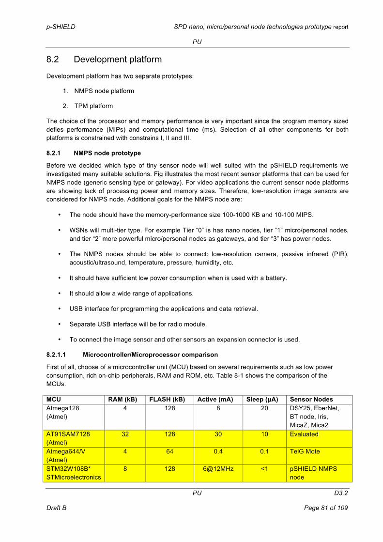
p-SHIELD SPD nano, micro/personal node technologies prototype report
PU
PU D3.2
Draft B Page 81 of 109
8.2 Development platform
Development platform has two separate prototypes:
1. NMPS node platform
2. TPM platform
The choice of the processor and memory performance is very important since the program memory sized defies performance (MIPs) and computational time (ms). Selection of all other components for both platforms is constrained with constrains I, II and III.
8.2.1 NMPS node prototype
Before we decided which type of tiny sensor node will well suited with the pSHIELD requirements we investigated many suitable solutions. Fig illustrates the most recent sensor platforms that can be used for NMPS node (generic sensing type or gateway). For video applications the current sensor node platforms are showing lack of processing power and memory sizes. Therefore, low-resolution image sensors are considered for NMPS node. Additional goals for the NMPS node are:
• The node should have the memory-performance size 100-1000 KB and 10-100 MIPS.
• WSNs will multi-tier type. For example Tier “0” is has nano nodes, tier “1” micro/personal nodes, and tier “2” more powerful micro/personal nodes as gateways, and tier “3” has power nodes.
• The NMPS nodes should be able to connect: low-resolution camera, passive infrared (PIR), acoustic/ultrasound, temperature, pressure, humidity, etc.
• It should have sufficient low power consumption when is used with a battery.
• It should allow a wide range of applications.
• USB interface for programming the applications and data retrieval.
• Separate USB interface will be for radio module.
• To connect the image sensor and other sensors an expansion connector is used.
8.2.1.1 Microcontroller/Microprocessor comparison
First of all, choose of a microcontroller unit (MCU) based on several requirements such as low power consumption, rich on-chip peripherals, RAM and ROM, etc. Table 8-1 shows the comparison of the MCUs.
MCU RAM (kB) FLASH (kB) Active (mA) Sleep (µA) Sensor Nodes Atmega128 (Atmel)
4 128 8 20 DSY25, EberNet, BT node, Iris, MicaZ, Mica2
AT91SAM7128 (Atmel)
32 128 30 10 Evaluated
Atmega644/V (Atmel)
4 64 0.4 0.1 TelG Mote
STM32W108B* STMicroelectronics
8 128 6@12MHz <1 pSHIELD NMPS node
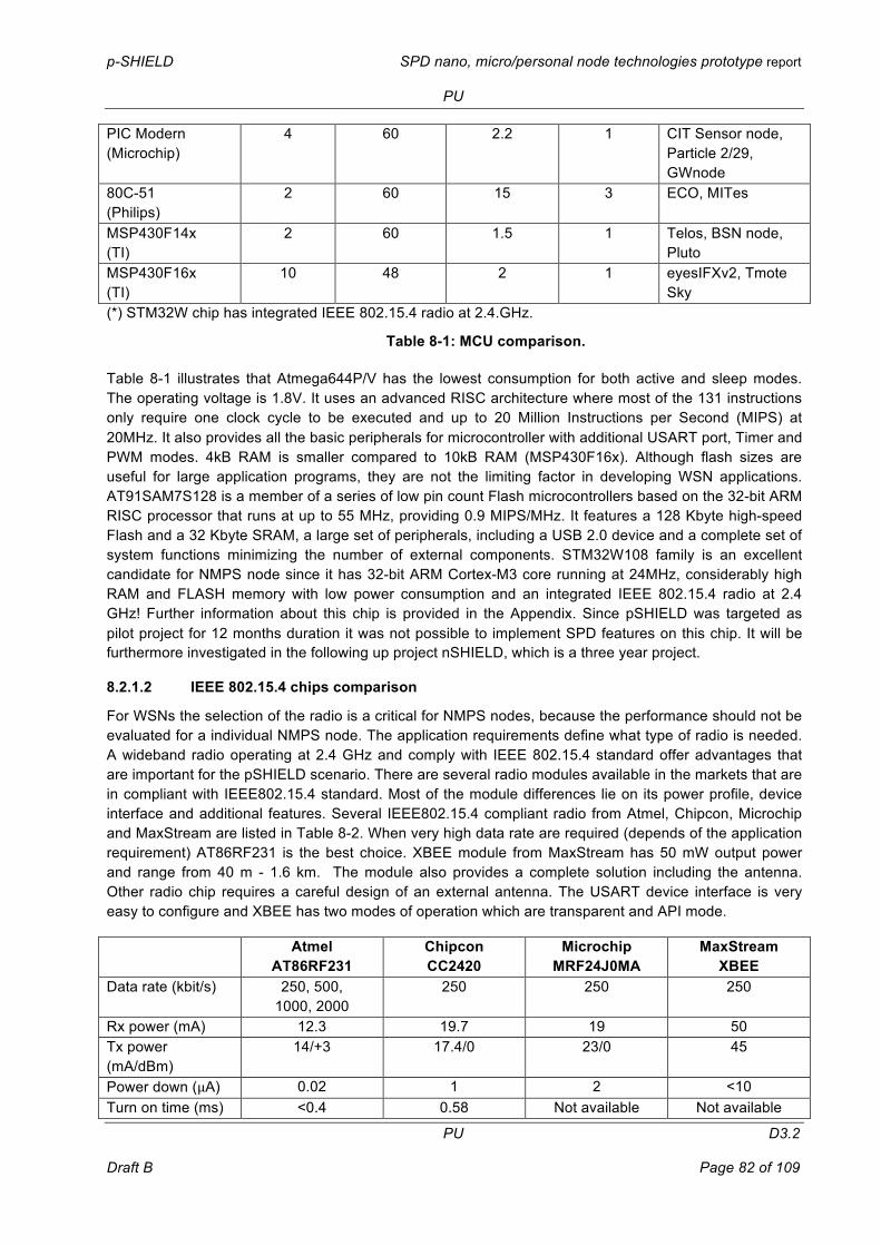
p-SHIELD SPD nano, micro/personal node technologies prototype report
PU
PU D3.2
Draft B Page 82 of 109
PIC Modern (Microchip)
4 60 2.2 1 CIT Sensor node, Particle 2/29, GWnode
80C-51 (Philips)
2 60 15 3 ECO, MITes
MSP430F14x (TI)
2 60 1.5 1 Telos, BSN node, Pluto
MSP430F16x (TI)
10 48 2 1 eyesIFXv2, Tmote Sky
(*) STM32W chip has integrated IEEE 802.15.4 radio at 2.4.GHz.
Table 8-1: MCU comparison.
Table 8-1 illustrates that Atmega644P/V has the lowest consumption for both active and sleep modes. The operating voltage is 1.8V. It uses an advanced RISC architecture where most of the 131 instructions only require one clock cycle to be executed and up to 20 Million Instructions per Second (MIPS) at 20MHz. It also provides all the basic peripherals for microcontroller with additional USART port, Timer and PWM modes. 4kB RAM is smaller compared to 10kB RAM (MSP430F16x). Although flash sizes are useful for large application programs, they are not the limiting factor in developing WSN applications. AT91SAM7S128 is a member of a series of low pin count Flash microcontrollers based on the 32-bit ARM RISC processor that runs at up to 55 MHz, providing 0.9 MIPS/MHz. It features a 128 Kbyte high-speed Flash and a 32 Kbyte SRAM, a large set of peripherals, including a USB 2.0 device and a complete set of system functions minimizing the number of external components. STM32W108 family is an excellent candidate for NMPS node since it has 32-bit ARM Cortex-M3 core running at 24MHz, considerably high RAM and FLASH memory with low power consumption and an integrated IEEE 802.15.4 radio at 2.4 GHz! Further information about this chip is provided in the Appendix. Since pSHIELD was targeted as pilot project for 12 months duration it was not possible to implement SPD features on this chip. It will be furthermore investigated in the following up project nSHIELD, which is a three year project.
8.2.1.2 IEEE 802.15.4 chips comparison
For WSNs the selection of the radio is a critical for NMPS nodes, because the performance should not be evaluated for a individual NMPS node. The application requirements define what type of radio is needed. A wideband radio operating at 2.4 GHz and comply with IEEE 802.15.4 standard offer advantages that are important for the pSHIELD scenario. There are several radio modules available in the markets that are in compliant with IEEE802.15.4 standard. Most of the module differences lie on its power profile, device interface and additional features. Several IEEE802.15.4 compliant radio from Atmel, Chipcon, Microchip and MaxStream are listed in Table 8-2. When very high data rate are required (depends of the application requirement) AT86RF231 is the best choice. XBEE module from MaxStream has 50 mW output power and range from 40 m - 1.6 km. The module also provides a complete solution including the antenna. Other radio chip requires a careful design of an external antenna. The USART device interface is very easy to configure and XBEE has two modes of operation which are transparent and API mode.
Atmel AT86RF231
Chipcon CC2420
Microchip MRF24J0MA
MaxStream XBEE
Data rate (kbit/s) 250, 500, 1000, 2000
250 250 250
Rx power (mA) 12.3 19.7 19 50 Tx power (mA/dBm)
14/+3 17.4/0 23/0 45
Power down (µμA) 0.02 1 2 <10 Turn on time (ms) <0.4 0.58 Not available Not available

p-SHIELD SPD nano, micro/personal node technologies prototype report
PU
PU D3.2
Draft B Page 83 of 109
Device interface SPI SPI SPI USART IEEE 802.15.4 HW support
FCS, CCA, RSSI, ED and LQI
RSSA, LQI RSSA, LQI RSSI
Antenna External External Integrated PCB Integrated Whip
Table 8-2: IEEE 802.15.4 chips comparison
8.2.1.3 Comparison of sensor node platforms
Figure 8-2 shows some recent sensor node platforms that are positioned with respect to the processor performance (MIPS) and memory size (kB). In the region low-bandwidth are typical sensor nodes and in high-bandwidth are extremely powerful gateway nodes. The Atmega128 (see Table 8-1) microcontroller is frequently used, but it can’t offer good performance for images. It use 8-bit architecture comparing to AT91SAM7128 which use 32-bit ARM7 processor.
Performance (MIPS)
Mem
ory
(kB
)
BT node
Telos
Spec
Medusa Mk II
WINS Hidra
Pico Node
Intel node 2
10 100
1
10
100
1000
10000
1 1000
Low-bandwidth High-bandwidth
Figure 8-2: Comparison of sensor node platforms.
Comparing cycles to read/write, Atmega128 require 74 cycles per pixel, which means clocked at 48 MHz it would require 0.12 s. AT91SAM7128 require 56 cycles per pixel, which means clocked at 4 MHz it would require 0.12 s. This reduction for factor 16 in execution time is big advantage at almost the same power consumption. Finally, Atmega128 don’t have sufficient memory to store the frames and any result. Intel Mote 2 sensor node platform48 has more memory and computational capabilities but it has higher power consumption and it is more expensive. For these reasons it is not suitable for large network deployment. However, it is can be used49 for BAN (Body Area Network). For NMP nodes we need a node between these two extreme, low and high-bandwidth. Medusa Mk II has two microcontrollers50 and radio 48 http://wsn.cse.wustl.edu/images/c/cb/Imote2-ds-rev2_2.pdf
49 http://netlab.boun.edu.tr/WiSe/lib/exe/fetch.php/courses:492_final_report_onur_dundar.pdf
50 http://aceslab.org/sites/default/files/Koushanfar_SensorNetArch_2005.pdf

p-SHIELD SPD nano, micro/personal node technologies prototype report
PU
PU D3.2
Draft B Page 84 of 109
TRF1000 (compatible with IEEE 802.15.4), which make it less attractive due to added complexity, which has drawback into cross-layer optimisations. Starting from the above SoA (state-of-art) we were looking for new sensor node platforms suitable for NMP node prototypes. Before, we decide which processor is suitable for an NMPS node it is important to highlight some restriction regarding the camera. The current generation cameras have a minimum resolution of 1280x1024 (1.3 megapixels). Such camera requires much memory and it is not suitable for NMPS node. In smart phone is used low-resolution camera CIF51 (352 x 288) and VGA (640 x480). Agilent ADMC-1670 is an excellent candidate with CIF 352 x 352.
8.2.1.4 NMPS node prototype evaluation
The research group of Stanford University investigated sensor nodes that use a 32-bit ARM microcontroller and CC2420 radio52. A comprehensive platform for WSNs that use TinyNode composed of MSP430F1611 microcontroller and XE1205 radio is proposed for environmental monitoring, parking management53, etc. Cookie sensor node uses a architecture, which is SW reprogrammable and HW reconfigurable54. It is designed to provide flexibility and adaptability by applaying modularity at the HW level trough a layered PCB structure. Similar layered structure is Tyndall node55. Modularity allows dividing and encapsulating the functionalities included in the node. By exploring in space different layers it is possible to adapt the node design to evolving technologies and standards, or by changing a layer that depends of the application. The four layers in Cooki sensor node are:
• 8051 microcontroller: Delivering up to 100 MIPS peak throughput, Silicon Labs’ 8-bit 8051 MCUs can satisfy the performance needs of many embedded applications more economically than costlier 16- or 32-bit MCUs. It has 10 nA sleep mode power consumption.
• Communications: ETRX2 from Telegesis is a ZigBee radio.
• Sensors: temperature, humidity, light, IR, etc.
• Power supply: a flexible solution for all voltage needed.
Signals from analog sensors are connected to ADC of the microcontroller. Signals from digital sensors are connected to FPGA, which carryout all processing for digital sensors.
ReconOS supports the execution and transparent interaction of hardware and software threads on a configurable system-on chip56. It supports both software and hardware threads with a single unified programming model. ReconOS is based on eCos, a widely-used real-time operating system (RTOS).
Figure 8-3 illustrates the prototype architecture that we investigated. The expansion interface unit is used to connect and evaluated different NMPS node elements like sensors, TPM modules, etc. For example we investigated the image sensors: Agilent ADMC-1670 CIF, ADNS-3060 concurrently by using two 51 http://psi.praeger.com/pdfs/whitepapers/PixelsandRecordSpeedandCIF.pdf
52 Ian Dowes e tal., “Development of a mote for wireless sensor networks,” COGnitive Systems with Interactive Sensors Conference, Paris, France (15-17 Mar. 2006)
53 H. Dobois Ferrire e tal, “TinyNode: A Comprenhesive Platform for WSN Applications,” 2006.
54 Y.E. Krateva et al., “Embedded Runtime Reconfigurable Nodes for Wireles Sensor Networks Applaictions,” IEE Sensor Journal, vol. 11, no. 9, Sept. 2011.
55 http://cora.ucc.ie/bitstream/10468/157/1/CS_AutomatedAV2009.pdf
56 http://www.cs.uni-paderborn.de/fileadmin/Informatik/AG-Platzner/publications/luebbers07_fpl/luebbers07_fpl.pdf
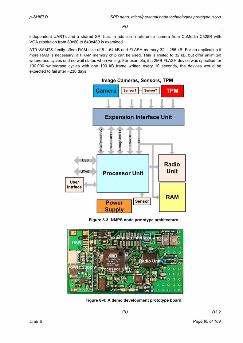
p-SHIELD SPD nano, micro/personal node technologies prototype report
PU
PU D3.2
Draft B Page 85 of 109
independent UARTs and a shared SPI bus. In addition a reference camera from CoMedia C328R with VGA resolution from 80x60 to 640x480 is examined.
AT91SAM7S family offers RAM size of 8 – 64 kB and FLASH memory 32 – 256 kB. For an application if more RAM is necessary, a FRAM memory chip can be used. This is limited to 32 kB, but offer unlimited write/erase cycles ond no wait states when writing. For example, if a 2MB FLASH device was specified for 100.000 write/erase cycles with one 100 kB frame written every 10 seconds, the devices would be expected to fail after ~230 days.
Processor Unit RadioUnit
RAM
Expansion Interface Unit
IRQ/Timer/PCK
ADC/GIPO
Debug/UART1
UART0
SPI
UserIntrface
USB
JTAG
Power Supply
Camera
Sensor
TPMSensor1 Sensor7...
Image Cameras, Sensors, TPM
Figure 8-3: NMPS node prototype architecture.
Power SupplyUnit
USBExpansion Interface Unit
Processor Unit
Radio Unit
Figure 8-4: A demo development prototype board.

p-SHIELD SPD nano, micro/personal node technologies prototype report
PU
PU D3.2
Draft B Page 86 of 109
8.2.1.5 Design and implementation of a trusted NMPS node
8.2.1.5.1 TPM unit
The pSHIELD project aims to include trusted features in the sensor node design. TCG proposed TPM modules to enhance security of the devices. In section 5.1.4.4 we introduced security architecture for a sensor node. This can be made by an ASIC design, but it is not targeted for a prototype design in pSHIELD. The way forward was to design a separate TM module. The contribution for trusted NMPS node of this deliverables includes the following:
1. Design of a trusted TPM platform for NMPS nodes, which include standard TPM chip. It is needed for cryptography (e.g., PKC, or ECC) and remote attestation in WSNs.
2. Extensive evaluation of trusted TPM unit in terms of cryptography algorithms, computation time, power consumption, cost, etc.
3. A proof-of-concept to use such trusted NMPS node for different applications where security enhancements are required (key management, secure SW update, secure remote attestation, etc).
The objective of a TPM is to provide a hardware-based root of trust for a device. For example, TPM has
• Cryptography operation engine – TPM is programmed with a unique RSA key pair and the private part never
leaves nonvolatile protected memory – RSA engine for signature generation and message decryption – Secure Hash Algorithm (SHA) Engine – Random Number Generation (RNG)
• Platform Configuration Register (PCR)
– Stores integrity-sensitive messages in regard to platform environment – Located in nonvolatile protected memory (temper-proof)
For the microcontroller we selected AT91SAM7128 and for TPM Atmel AT97SC3203S57 illustrated in Figure 8-5 (block diagram) and Figure 8-6 (demo board). It is a fully integrated security module for embedded systems. TPM unit is connected through extension unit in Figure 8-3 by using I2C interface.
57 http://www.atmel.com/dyn/resources/prod_documents/5132s.pdf

p-SHIELD SPD nano, micro/personal node technologies prototype report
PU
PU D3.2
Draft B Page 87 of 109
33 MHzOscilator
Toward Extension Interface
on NMPS Node
Optional power3.3 Voltage Reg.
Power Switch Vcc
SB3VRESET
AT97SC3203S
Figure 8-5: Block diagram of Amtel AT97SC3203S TPM.
Figure 8-6: TPM Amtel AT97SC3203S unit.
A TMM is a micro-controller with additional security features that can store and protect sensitive information used to authenticate a trusted platform, e.g., passwords or cryptographic key. In contrast to a smart card, a TPM is usually logically (and physically) linked to a device or platform, not to a person, and provides additional secure hardware components.
Figure 8-6 illustrated TPM unit. Atmel AT97SC3203S TPM chip size is 6.1 x 9.7 mm and cost 4.5 $ (large quantity. It can be easily integrated into NMPS node. With this we will achieve a compact NMPS node solution for many different applications.
8.2.1.5.1.1 Selection of PKC
In Chapter 5 were discussed different security aspects for NPNS nodes. RSA and Diffie Hellman are mostly used PKC on the Internet. In the past these cryptography techniques were considered as infeasible for WSNs. In 2004 Watro et al proposed TinyPK. Due to smaller public key the security level

p-SHIELD SPD nano, micro/personal node technologies prototype report
PU
PU D3.2
Draft B Page 88 of 109
was severely compromised. MiniSec58 provides confidentiality and authenticity for both unicast and broadcast messages. It assumes that a share key is kept safe at all nodes! Therefore, MiniSec needs an effective key establishment and management scheme. Lui and Ning in 2008 proposed TinyECC. Today research community intensively investigate ECC as a promised solution for energy-constrained sensor nodes. In 2010 When Hu et al demonstrated that RSA-based security is feasible on a WSN node. Thus today, we have still to investigate and compare the recent research results for PKC techniques by using RSA or ECC.
8.2.1.5.1.2 Functionality of TPM
The most relevant functionalities of TPM for WSNs are:
• Cryptography operation engine (COE):
The cryptography operation can be made by RSA or ECC for signature generation and message decryption, SHA engine and RNG. Every TPM is programmed with unique RSA or ECC key pair. The private part never leaves nonvolatile storage area of TPM. When a nod is captured by an attacker the private part key would not be available to the attacker.
• Platform configuration register (PCR):
TPM has a number (16) of PCR. The content stored in each PCR is a digest of messages in regard to the platform environment. PCRs are located in the nonvolatile storage area and hence cannot be tempered with.
For example, if RSA is used the symmetric keys are typically generated by RNG. If an attacker can extract the initial random symmetric key, then it is possible for the attacker to compute all past and future random symmetric keys. Therefore, a strong RNG is very important for the effectiveness of symmetric key operations. RNG may be complaint with FIPS 104-2. The primitive random integer value is 2322 1 4.294.967.295− = . SHA-1 is used for TPM commands. It produces collision-free 20-byte hashed
digest regardless of the input message. SHA-1 is frequently used because it is one-way function which is computationally infeasible to invert and used to develop the HMAC (Hashed Message Authentication Code). HMAC is an extension of SHA-1. Because the shared secret is not available to third parties an attacker cannot replay the intercepted message due to the antireplay nonce or forge a valid HMAC for tempered message to circumvent the HMAC check. PCR value can be preserved even the TPM is turned off.
8.2.1.5.2 Mobile Trusted Modules (MTM)
TCG Mobile Phone Work Group specifies a new concept to enable trust into future mobile devices59. An approach for the practical design and implementation of this concept and how to deploy it to a trustworthy operating platform is proposed60. Currently, we are studying the possible solution of MTM.
58 http://sparrow.ece.cmu.edu/group/pub/luk_mezzour_perrig_miniSec.pdf
59 http://hackipedia.org/Digital%20Rights%20Management/Trusted%20Computing/hardware/pdf/tcg-mobile-trusted-module-1.0.pdf
60 A. U. Schmidt et al., “On the deployment of Mobile Trusted Modules, IEEE WCNC 2008, Las Vegas, USA, 31 March - 2 April 2008.
p-SHIELD SPD nano, micro/personal node technologies prototype report
PU
PU D3.2
Draft B Page 89 of 109
9 Confidentiality, Integrity, Authenticity, Availability and System Integrity in WSNs
WSNs are application dependent and they are designed for real-time collection and analysis. They are well suited for monitoring and surveillance applications. For RT of dangerous materials security is a crucial issue. In this chapter we will focus on CIAA concept to proof that the NMPS node prototype will satisfy the security requirements for pSHIELD.
Confidentiality is the ability to conceal messages from a passive attacker so that any message communicated via the WSN remains confidential. This is the most important issue in network security. A sensor node should not reveal its data to the neighbours.
Integrity of data in WSNs is needed to ensure the reliability of the data and refers to the ability to confirm that a message has not been tampered with, altered or changed. Even if the network has confidentiality measures, there is still a possibility that the data integrity has been compromised by alterations.
Authentication ensures the reliability of the message by identifying its origin. Attacks in WSNs do not just involve the alteration of packets; adversaries can also inject additional false packets. Data authentication verifies the identity of the senders and receivers. Data authentication is achieved through symmetric or asymmetric mechanisms where sending and receiving nodes share secret keys. Due to the wireless nature of the media and the unattended nature of sensor networks, it is extremely challenging to ensure authentication.
Availability determines whether a sensor node has the ability to use the resources and whether the network is available for the data/messages to communicate. However, failure of the Gateway or cluster head node availability will eventually threaten the entire WSN. Thus availability is of primary importance for maintaining an operational network.
The security mechanisms are used to detect, prevent and recover from security attacks. A low-level security is achieved by key establishment and trust setup, secrecy and authentication, privacy, robustness to communication DoS, secure routing, and resilience to node capture. High-level security is achieved by secure group management, intrusion detection and secure data aggregation. A TPM attached to a NMPS node, and act as root of trust of the node platform given its tamper resistance features. In section 8 is demonstrated that it is designed to perform cryptographic functions such as RSA, RNG and SHA1. The core functionality of TPM is integrity measuring and storage, and reporting to the node platform. The integrity measuring and storage are achieved through a set of PCRs, internal to TPM. It was mentioned before in section 8.2.1.5.1.1 each PCR value is 20-byte cumulative hash digest (SHA1 value) of a number of measure platform integrity metrics. Altogether the PCRs record the integrity status of the node platform from booting to OS loading to applications loading. An update to a PCR value is through what is termed extending the PCR, which is described as
[ ] [ ]1( )PCR i SHA PCR i newlymeasuredvalue←
where i is the number of the PCR being updated.
9.1 Security enhancements: performance evaluation
In this section we are summarizing the performance of a NMPS node platform equipped with a TPM unit. As part of our study in section 7 the possible final implementation of RSA or ECC for NMPS node is still under investigation. However, the reported results are encouraging that such cryptography can be used

p-SHIELD SPD nano, micro/personal node technologies prototype report
PU
PU D3.2
Draft B Page 90 of 109
successfully for energy-constrained sensor nodes. The results show that the TPM chip can reduce the computational time of RSA encryption by a factor of 8000. The SW RSA implementation is impractical using embedded microcontroller Atmega128.
It is recently approved that for a sensor node that used TPM with RSA cryptography for which only 10% of battery energy is available for security operations performed twice per day the expected node life time is 7.4 years! This proof significantly shows the use of TPM for WSNs sensor nodes is feasible.
9.1.1 Experiments
It is known that symmetric key cryptography consumes less energy than RSA (asymmetry keys, encryption key is different from decryption key). For example XTEA encryption consume approximately 10 times less energy compared to HW RSA encryption, and approximately 12.000 times less energy compared to SW RSA encryption. A strategy to adopt will be for nano nodes to use symmetric cryptography, and for critical applications like the pSHIELD scenario, asymmetric cryptography should be used. For example, asymmetric cryptography can be used to exchange a new symmetric key daily or hourly (this is called rekey process61,62,63,). An application can select to store the session keys in TPM.
An NMPS node A requests a new symmetric key from a NMPS node B, i.e., Gateway (GW). Node A initiates this process hourly or daily by generating a random number Na (nonce) and encrypts the nonce along with the request (Req) command using GW’s public key (Pkgw) before transmitting it to the GW. The purpose of nonce is to defend against reply attacks. After receiving Req message from Node A, the GW decrypts the message with its private key Sgw. The GW responds to the Req command by generating a new symmetric session key Kba and encrypts it together with Na using a public key Pka before transmitting it to node A. Node A decrypts the message the from the GW with it its private key Ska and obtains the new symmetric key Kba. Nose A and the GW can then use Kba for future communications as in Figure 9-1. Therefore, link level secure communications can be achieved by passing the returned cipher over the radio. In the case that the key are stored in Ram or EEPROM it is not secure, because that the information can be extracted from EEPROM and RAM in 1 min. Therefore, storing the key in TPM chip for these infrequent operations is more safely.
Group key establishing cn be achieved by combination of sensor node symmetric session key request operation and sensor node symmetric session key assignment operation. For example if node A wants to communicate with node B and C, node A will request a new group session key from the GW via the session key request operation. After receiving the key request operation from Node A, the GW generates a new symmetric key Kabc. The GW assigns Kabc to the Node B and C via two session key assignment operations before transmitting Kabc to Node A. Finally, Node A, B and C we perform secure communications using the group session key Kabc.
61 http://xtrmntr.org/priikone/docs/ike.pdf
62 http://conferences.sigcomm.org/co-next/2009/workshops/student/papers/Shen.pdf
63 http://mcn.cse.psu.edu/paper/zhang/adhoc09.pdf

p-SHIELD SPD nano, micro/personal node technologies prototype report
PU
PU D3.2
Draft B Page 91 of 109
Node A GW
Generation a random number Na
Decrypts with Ska
Decrypting with Sgw Generate a new session key
Kba
E(Pkgw,Na, Req)
E(Pka,Na, Kba)
Communication with Kba
E(Pkgw,Na, Req)
Kabc
KabcKabc
Kabc
a) b)
Kabc
Kabc
GW
Figure 9-1: Symmetric session key request operation with trusted NMPS nodes: a) between Node A and GW, b) between Nodes A, B and C grace a secession key Kabc generated by GW on the request from Node A.
9.1.1.1 Attack models
With respect to the possible attacks explained in section 4.1.3.1 there are different attack models. Here, we are mostly concerned for integrity. Therefore, we can define the following attack models.
1. The attack initiated from a radio signal which try to reprogram sensor node with malicious intent.
2. The physical attacks which completely take over sensors by plugging in wired cables.
For example, through radio channel can be modified the functional modules of a sensor. The second model is relevant for changing middleware or OS, which are hard coded in the HW. By reprogramming sensor nodes through radio signals is possible in the following cases:
• Listen to the data being transmitted through a node • Introduce corrupt data into the WSN • Act as sink and discard all the data passing through the node. • Deplete the node of its resources • Keep transmitting garbage data; thereby deplete energy of entire network or occupancy the
communication channel.
The first assumption is that an attacker has a powerful PC computer with powerful computational resources. The attack may be an external or internal. Injecting malicious packets into the network, replay previously intercepted packets, or impersonate other nodes is an external attack for eavesdropping the information. DoS are external attacks were explained in section 4. The attacker can compromise some nodes to attack the rest of the network (internal attack). Compromised sensor nodes are considered as legitimate nodes in the WSN before they are detected and removed. However, despite nodes are being compromised, the cryptographic information stored in TPM could not be learned because TPMs are temper-proof HW. For the purpose of secure bootloading the microcontroller is configured via the fuses so that, on reset, control is transferred to the initialisation code within bootloader segment. Then the
p-SHIELD SPD nano, micro/personal node technologies prototype report
PU
PU D3.2
Draft B Page 92 of 109
initialisation code performs a TPM clear state reset, which clear all TPM configurations including PCR value. We can use a remote attestation protocol to test the system integrity of a node and to defend against over-the-air malicious code injection attacks.
We shows that by utilising commercial TPM HW techniques is possible to design a trusted NMPS node that provide essential security services such as message confidentiality, integrity, authenticity and system integrity based on RSA or ECC cryptography techniques. The results shows that such node can provide services within the computational, memory and energy limits that apply to pSHIELD WSN nodes. HW approach offer secure storage of the private key and support for system configuration checking. We have demonstrated there is possible to achieve remote attestation, symmetric key management, secure SW update, etc.
9.1.2 Future work
Integrity of a node can be verified by an attestation protocol, which used TPM as was proposed in the previous section. By to enable a WSN operator to react to tempering attempts, information about the node integrity needs to be exchanged through the network. If such information is exchanged overtly, attacker may be aware of the fact that the network is being monitored. Analyses of exchanged information may even reveal how often such information is exchanged and if no appropriate cryptography countermeasures are taken, it may also be possible to tell what information is exchanged. The problem is that every integrity protocol needs a secure channel between devices. Recently was proposed a “covert channel” for hidden transportation of integrity monitoring messages. The current work presented in this deliverables will be extended toward a new approach for enhancing security regarding the system integrity.

p-SHIELD SPD nano, micro/personal node technologies prototype report
PU
PU D3.2
Draft B Page 93 of 109
10 Conclusions This deliverable summarises the SPD attributes and functionalities for NMPS nodes that composed a pSHIELD sub-WSN. One of the main aims of this document was to provide an extended view of the SPD concerns in ESs design and implementation for the pSHIELD system. It is essential to consider the fundamental and often application-specific characteristics of ESs and the particular requirements developed in D2.3.1.
Our goal was to provide various mechanisms for ensuring and maintaining the security and dependability of sensed network data under the aforementioned adversary model. Specifically, we have the following goals:
• Security: To enhance data confidentiality, integrity authenticity and system integrity.
• Privacy: To enhance privacy because, WSNs are “tools” for collecting information, and an adversary can gain access to sensitive information either by accessing stored sensor data or by querying or eavesdropping on the network.
• Dependability: To enhance data availability against sensor failures and sensor compromises, i.e., minimizing the effect brought by individual sensor failures and compromises.
• Lightweight: The NMPS node security design should be lightweight as always in order to fit into the inherent resource-constrained nature of the sensor nodes.
Pervasive computing, ubiquitous computing and ambient intelligence are areas of a rapidly growing area of research and, especially in recent times. These terms also describe numerous innovative applications of computing. New types and integration of HW and SW are required to realize applications embedded in our daily life and work. A key aspect of pervasive computing involves embedding sensing, networking and computation into everyday objects and everyday life processes. The innovations include new concept systems that previously are not feasible but now feasible due to fundamental advances in SW/HW and networking. All this things were highlighted in prototypes design.
Based on a layered design approach proposed for the pSHIELD system/network and SPD service composition the existence of SPD nodes is essential. Therefore, a considerable effort was made for designing NPM SPD node prototypes. In this document, we firstly reviewed the weakness of previous proposed SPD schemes and pointed out the major concerns for security of WSNs via formal proof. In particular we highlighted possible WSN applications we a focus on RTCI scenario, their network architecture, their hardware specifications and their security vulnerabilities. We also outlined the major threats associated with WSNs. In the literature survey, we emphasized also the work to date conducted by researchers in the areas:
1. NMP Node Technologies
2. Wireless Sensor Networks
3. Firmware, Secure SoC, and Trust
4. Power Supply Protections
5. ECC for NMP Nodes
6. NMP Node: prototypes
7. Confidentiality, Integrity, Authenticity, and System Integrity in WSNs

p-SHIELD SPD nano, micro/personal node technologies prototype report
PU
PU D3.2
Draft B Page 94 of 109
Securing a WSN needs to make the network support all security properties: confidentiality, integrity, authenticity and availability on which we focus our work for proof-of-concept. We showed that efficient software updating is in many ways one of the most challenging features to provide on a WSN. It requires reliability large amounts of data to be reliably disseminated to the nodes, sophisticated mechanisms to minimize the cost of this dissemination, and aggregated status to be returned to a host. It may also require tracking of software failures and recovering from its failures in a network-wide manner. It must provide support to handle network partitioning, node failures, software failures, data transmission failures and other intermittent and persistent faults.
In this document we have identified scientific challenges with respect to security and dependability that need to be solved to make WSNs a ready to use technology for RTCI protection scenarios. In order to cope with those challenges we apply a multi-disciplinary, multi-technology and a vertical network approach, where we do not focus on a single layer or subsystem, but consider the whole system in all its facets. We are currently working on the further implementations of the concepts introduced in this document.
EDs need both an efficient and a secure implementation of cryptographic algorithms. In this deliverable we show a typical top-down approach for secure and efficient implementation of embedded systems. We outline the security pyramid by illustrating the five primary abstraction levels in an embedded system. Focusing only on all levels we show how the design can be implemented to be both efficient and secure. Therefore, security cannot be solved at a single security abstraction layer, but rather is a system problem spanning multiple abstraction levels or functional layers. For the future ESDs solution we need to change the ordinary strategy and consider the secure ES design not as an ad-hoc process, but as a systematic top-down approach. Here, we addressed some of the common issues related to this topic.
It was showed that firmware verification would best be done using hash functions and digital signatures. This would only require the system to store a public key that an attacker could not benefit from knowing. To prevent cryptanalysis and brute-force attacks recommendations from NIST were used. From the recommendations we chose SHA-224 to hash the firmware image and RSA 2048 as digital signature algorithm. ECC is becoming a powerful cryptographic scheme. Because of its efficiency and security is a good alternative to cryptosystems, like RSA and DSA, not just in constrained devices, but also on powerful computers. ECC is very important in the field of low-resource devices such as smart cards and Radio Frequency Identification (RFID) devices because of the significant improvements in terms of speed and memory compared to traditional cryptographic primitives (e.g. RSA). The main contributions are:
• We have presented a generalized NMP node architecture that addresses key issues that arise when building a WSN device that must meet most of the pSHIELD node requirements. Based on this generalized NMP node architecture we investigated some practical implementation as NMP prototypes.
• We also presented the development of a new NMPS node platform for WSNs. It has investigated potential applications and determined necessary characteristics for a NMPS node prototype, primarily sufficient processing capability and memory. These characteristics have been used to show that current sensor platforms are not suitable for more power sensing applications (e.g., images). A new NMPS node is proposed. In this project, we develop a new NMP platform prototype based on the existing WSN platform as our guideline and choose low power and an easy to interface devices to provide a multi-sensor platform (message, data, video) together with an embedded operating system (TinyOS, Contiki, Hydra). SPD design issues were examined on the attack models.
• We have utilized TPM technology to create a trusted node that provides security services such as confidentiality, integrity, authenticity and system integrity. In parallel we also showed that SW
p-SHIELD SPD nano, micro/personal node technologies prototype report
PU
PU D3.2
Draft B Page 95 of 109
solutions are possible. This research work is planned for nSHILED project. The main reason for that are advantages offered by embedded runtime reconfigurable nodes for WSNs applications. It is constrained by the application-specific scenarios. Reconfigurable nodes can adapt these differences from one to other scenario by maintaining a generic node design. The SPD functions can be dynamically allocated by runtime HW reconfiguration and SW updates.
• We have proposed different power supply solution for NMP nodes. Where the size is reduced, the best solution for sensor nodes will be the one based on a rechargeable battery combined with an ultracapacitor (hybrid battery). Thus, the battery lifetime will be extended since the maximum expected power consumption in this kind of nodes is around 150mW. An ultracapacitor is useful during transmission/reception operations, where it is expected the maximum power consumption. Although power consumption of micro nodes is higher, they are slightly bigger than nano nodes so a solution based on a rechargeable battery combined with a solar panel could be considered. If most of the time, these nodes are in low power consumption mode, a method based on harvesting power from vibrations could be implemented. Both protection boards have been tested in order to verify that system is protected against over voltages, overloads, short circuit or over temperatures. Both designs have fulfilled the defined requirements since nodes have integrated not only the necessary protections but also a mechanism to plug-unplug different sub-systems and a sensor to monitor power consumption.
Finally, in this document we presented some of the issues related to SPD in WSN. We provided a comprehensive study regarding the final requirements (D2.1.2, D2.2.2, D2.3.2), different kind of well-known attacks and some of the proposed solutions as countermeasure for the security attacks on WSNs. We also emphasized on the ESs security where industry and research community has recently given a lot of attention. We have touched upon the concept of trust and reputation based security analysis in WSNs. With this, we attempt to make the main focus here also on privacy preservation aspects of WSNs. Therefore, our additional effort was to bring that privacy protection problem in WSNs. In that regard, we have provided detailed description of some of the important schemes and present the privacy preservation of WSNs both from pSHIELD functional and requirement perspectives.

p-SHIELD SPD nano, micro/personal node technologies prototype report
PU
PU D3.2
Draft B Page 96 of 109
11 Appendix: STM32 chip
11.1 The Cortex™-M3 based STM32
11.1.1 The ARM Cortex - M3
The ARM Cortex – M3 processor, the first of the Cortex generation of processors released by ARM in 2006, he is designed to target the 32 – bit microcontroller market. The Cortex – M3 processor provides excellent performance at low gate count and comes with many new features previously available only in high – end processors. The Cortex-M3 addresses the requirements for the 32 – bit embedded processor market in the following ways:
• Greater performance efficiency, allowing more work to be done without increasing the frequency or power requirements
• Low power consumption, enabling longer battery life, especially critical in portable products including wireless networking applications
• Enhanced determinism, guaranteeing that critical tasks and interrupts are serviced as quickly as possible but in a known number of cycles
• Improved code density, ensuring that code fits in even the smallest memory footprints • Ease of use, providing easier programmability and debugging for the growing number of 8-bit and
16-bit users migrating to 32-bit • Lower-cost solutions, reducing 32-bit-based system costs close to those of legacy 8-bit and 16-bit
devices and enabling low-end, 32-bit microcontrollers to be priced at less than 1 euro for the first time
• Wide choice of development tools, from low-cost or free compilers to full-featured development suites from many development tool vendors
The ARM Cortex-M3 processor offers significant benefits to system and software developers.
• Lower cost devices through smaller processing core, system and memories • Ultra low power consumption and integrated sleep modes • Outstanding processing performance for challenging applications • Fast interrupt handling for critical control applications • Platform security with optional integrated memory protection unit • Enhanced system debug for faster development • No assembler code requirement to ease system development • Wide application envelope encompassing ultra-low cost microcontrollers and high performance
SoC.
11.1.2 The Cortex-M3 Processor vs Cortex-M3-Based MCUs
The Cortex-M3 processor is the central processing unit (CPU) of a microcontroller chip. In addition, a number of other components are required for the whole Cortex – M3 processor – based microcontroller. After chip manufacturers license the Cortex – M3 processor, they can put the Cortex – M3 processor in their silicon designs, adding memory, peripherals, input/output (I/O), and other features. Cortex – M3 processor based chips from different manufacturers will have different memory sizes, types, peripherals, and features.

p-SHIELD SPD nano, micro/personal node technologies prototype report
PU
PU D3.2
Draft B Page 97 of 109
11.1.2.1 STM32 Cortex-M3 processor and core peripherals
The Cortex-M3 processor is built on a high-performance processor core, with a 3-stage pipeline Harvard architecture, making it ideal for demanding embedded applications as in Figure 11-1. The processor delivers exceptional power efficiency through an efficient instruction set and extensively optimised design, providing high – end processing hardware including single cycle 32x32 multiplications and dedicated hardware division.
Figure 11-1: STM32 Cortex - M3 implementation
To facilitate the design of cost – sensitive devices, the Cortex – M3 processor implements tightly-coupled system components that reduce processor area while significantly improving interrupt handling and system debug capabilities. The Cortex – M3 processor implements a version of the Thumb instruction set, ensuring high code density and reduced program memory requirements. The Cortex – M3 instruction set provides the exceptional performance expected of a modern 32 – bit architecture, with the high code density of 8 – bit and 16 – bit microcontrollers.
The Cortex – M3 processor closely integrates a configurable nested interrupt controller (NVIC), to deliver industry – leading interrupt performance. The NVIC includes a nonmaskable interrupt (NMI), and provides up to 256 interrupt priority levels. The tight integration of the processor core and NVIC provides fast execution of interrupt service routines (ISRs), dramatically reducing the interrupt latency. This is achieved through the hardware stacking of registers, and the ability to suspend load – multiple and store – multiple operations. Interrupt handlers do not require any assembler stubs, removing any code overhead from the ISRs. Tail – chaining optimization also significantly reduces the overhead when switching from one ISR to another.
To optimize low – power designs, the NVIC integrates with the sleep modes that include a deep sleep function that enables the STM32 to enter STOP or STDBY mode.
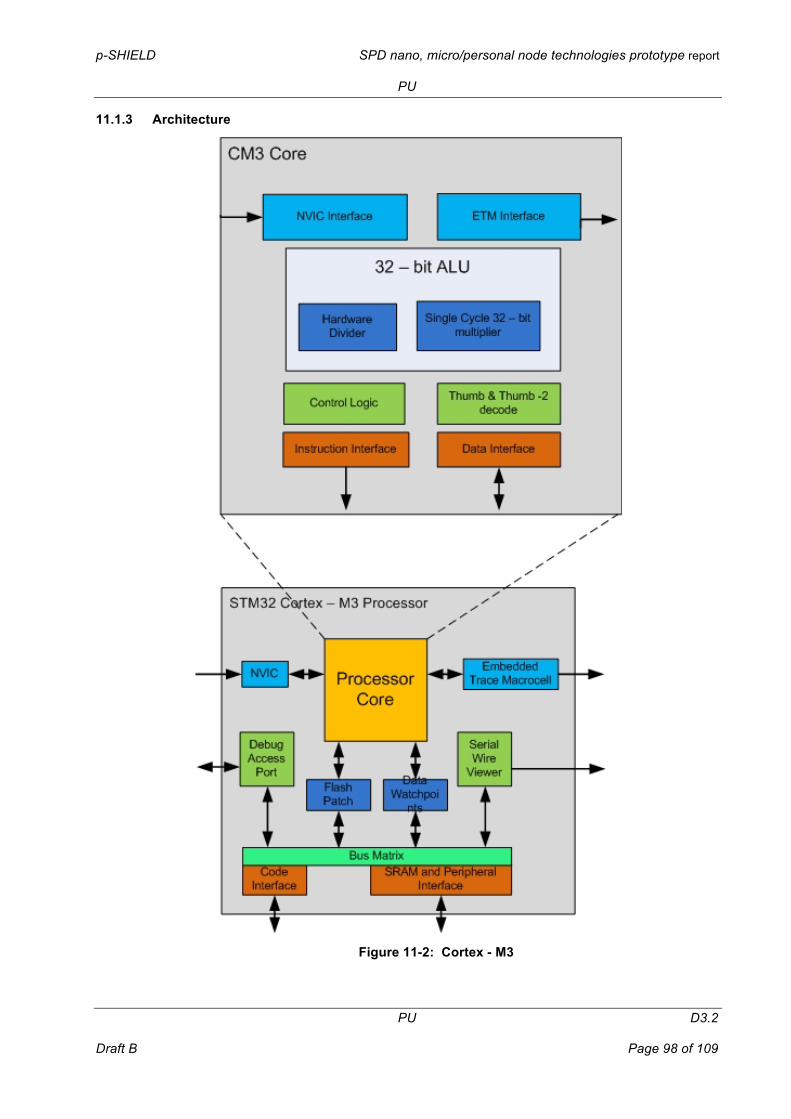
p-SHIELD SPD nano, micro/personal node technologies prototype report
PU
PU D3.2
Draft B Page 98 of 109
11.1.3 Architecture
Figure 11-2: Cortex - M3

p-SHIELD SPD nano, micro/personal node technologies prototype report
PU
PU D3.2
Draft B Page 99 of 109
11.1.3.1 ARM Cortex-M3 Processor Overview
The ARM Cortex – M3 processor integrates multiple system peripherals with a high-performance core to deliver unrivalled benefits in both cost sensitive and performance focused applications. The processor is fully synthesisable and is highly customizable enabling a wide range of physical interrupts and debug architectures to be implemented. Additionally the Cortex – M3 processor enables the optional integration of a fine – granularity Memory Protection Unit (MPU) and an Embedded Trace Macrocell (ETM).
11.1.3.2 ARM Cortex-M3 Core
The ARM Cortex – M3 processor is built on a high performance 3 – stage pipeline Harvard architecture core, making it ideal for demanding event driven applications. Exceptional power efficiency is delivered through extensive clock gating plus technology that improves performance per cycle including single cycle 32x32 multiplication and hardware division. Additionally the core has significantly reduced physical area through the implementation of a stack-based exception model. The Cortex – M3 processor implements the Thumb – 2 instruction set, a super – set of traditional Thumb instructions, which delivers both the performance of traditional 32 – bit code and the high code density of 16 – bit.
11.1.3.3 Nested Vectored Interrupt Controller (NVIC)
The Cortex – M3 processor closely integrates the core with a configurable interrupt controller to deliver industry – leading interrupt processing performance. In its standard implementation the NVIC supplies a Non Maskable Interrupt (NMI) plus 32 general purposes physical interrupts with 8 levels of pre – emption priority, however through simple synthesis choices the controller can be configured down to a single physical interrupt or up to 244. Additionally the number of levels of pre-emptive priority can be configured at synthesis up to 255.
11.1.3.4 Interconnect Matrix
The ARM Cortex – M3 processor integrates an AMBA AHB – Lite interconnect to support the system peripherals and reduce system integration complexity. The Bus Matrix delivers support for unaligned data accesses ensuring data is tightly packed into memory, significantly lowering SRAM requirements and system cost. Additionally the Cortex – M3 Bus Matrix implements atomic bit manipulation that enables system spinlocks and ensures the safe use of single-bit data representation in heavily interrupt drive applications.
11.1.3.5 Integrated Debug
The ARM Cortex – M3 processor implements a complete hardware debug solution enabling high system visibility of the processor through a traditional JTAG port or the 2 – pin Serial Wire Debug (SWD) port that is ideal for microcontrollers and other small package devices. For system trace the processor integrates an optional ETM alongside data watch points that can be configured to trigger on specific system events. To enable simple and cost effective profiling of these system events a Serial Wire Viewer (SWV) can export streams of standard ACSII data through a single pin. Flash Patch technology offers device and system developers the ability to patch errors in code from ROM to SRAM or Flash during both debug and run-time, potentially eliminating the need for costly response.
11.1.3.6 Optional Components
The ARM Cortex-M3 processor has two optional components:
Memory Protection Unit (MPU) — the fine grain MPU design enables applications to implement security privilege levels, separating code, data and stack on a task-by-task basis. Such requirements are becoming critical in many embedded applications such as automotive.

p-SHIELD SPD nano, micro/personal node technologies prototype report
PU
PU D3.2
Draft B Page 100 of 109
ETM —the Cortex-M3 ETM delivers unrivalled instruction trace capture in an area far smaller than traditional trace units enabling many low cost devices, such as MCUs, to implement it for the first time.
11.1.4 STM32F
The STM32 family of 32-bit Flash Microcontrollers is based on the breakthrough ARM Cortex™-M3 core - a core specifically developed for embedded applications. TheSTM32 family benefits from the Cortex-M3 architectural enhancements including the Thumb-2 instruction set to deliver improved performance with better code density, significantly faster response to interrupts, all combined with industry leading power consumption. ST is now the first leading MCU supplier to introduce a product family based on this core. The STM32 family is built to offer new degrees of freedom to MCU users. It offers a complete 32-bit product range that combines high performance, low power and low voltage, while maintaining full integration and ease of development.
The STM32F is the foundation of the STM32 family. The STM32F family of 32-bit Flash microcontrollers is based on the breakthrough ARM Cortex™-M3 core, specifically developed for embedded applications. They combine high performance with first-class peripherals and low-power, low-voltage operation. They offer the maximum integration at accessible prices with a simple architecture and easy-to-use tools.
With five lines, the STM32F1xx series provides perfectly balanced products for a wide range of applications in the industrial, medical and consumer markets. The following five lines are pin-to-pin, peripherals and software compatible:
• Value line STM32F100xx - 24 MHz CPU with motor control and CEC functions • Access line STM32F101xx - 36 MHz CPU, up to 1 Mbyte Flash • USB access line STM32F102xx - 48 MHz CPU with USB FS • Performance line STM32F103xx - 72 MHz, up to 1 Mbyte Flash with motor control, USB and
CAN • Connectivity line STM32F105/107xx - 72 MHz CPU with Ethernet MAC, CAN and USB 2.0 OTG
The new leading-edge STM32F2xx series combines advanced 90nm process technology with the innovative adaptive real-time memory accelerator (ART accelerator™) and the multi-layer bus matrix. This series achieves 150 Dhrystone MIPS when executing code from Flash at 120MHz with 188 µA/MHz dynamic power consumption.
• STM32 F-2 series: 120 MHz CPU with ART accelerator, 1 Mbyte Flash, Ethernet MAC, USB 2.0 HS OTG, camera interface, encryption.
The STM32F103xx high-density performance line family operates in the –40 to +105 °C temperature range, from a 2.0 to 3.6 V power supply. A comprehensive set of power-saving mode allows the design of low-power applications.
These features make the STM32F103xx high-density performance line microcontroller family suitable for a wide range of applications such as motor drives, application control, medical and handheld equipment, PC and gaming peripherals, GPS platforms, industrial applications, PLCs, inverters, printers, scanners, alarm systems video intercom, and HVAC.
The STM32 advantages:
• Leading-edge architecture with the latest Cortex-M3core from ARM • Superior and innovative peripherals • Low power/low voltage capability
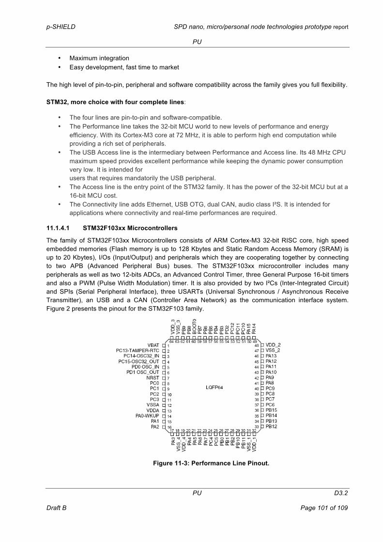
p-SHIELD SPD nano, micro/personal node technologies prototype report
PU
PU D3.2
Draft B Page 101 of 109
• Maximum integration • Easy development, fast time to market
The high level of pin-to-pin, peripheral and software compatibility across the family gives you full flexibility.
STM32, more choice with four complete lines:
• The four lines are pin-to-pin and software-compatible. • The Performance line takes the 32-bit MCU world to new levels of performance and energy
efficiency. With its Cortex-M3 core at 72 MHz, it is able to perform high end computation while providing a rich set of peripherals.
• The USB Access line is the intermediary between Performance and Access line. Its 48 MHz CPU maximum speed provides excellent performance while keeping the dynamic power consumption very low. It is intended for users that requires mandatorily the USB peripheral.
• The Access line is the entry point of the STM32 family. It has the power of the 32-bit MCU but at a 16-bit MCU cost.
• The Connectivity line adds Ethernet, USB OTG, dual CAN, audio class I²S. It is intended for applications where connectivity and real-time performances are required.
11.1.4.1 STM32F103xx Microcontrollers
The family of STM32F103xx Microcontrollers consists of ARM Cortex-M3 32-bit RISC core, high speed embedded memories (Flash memory is up to 128 Kbytes and Static Random Access Memory (SRAM) is up to 20 Kbytes), I/Os (Input/Output) and peripherals which they are cooperating together by connecting to two APB (Advanced Peripheral Bus) buses. The STM32F103xx microcontroller includes many peripherals as well as two 12-bits ADCs, an Advanced Control Timer, three General Purpose 16-bit timers and also a PWM (Pulse Width Modulation) timer. It is also provided by two I²Cs (Inter-Integrated Circuit) and SPIs (Serial Peripheral Interface), three USARTs (Universal Synchronous / Asynchronous Receive Transmitter), an USB and a CAN (Controller Area Network) as the communication interface system. Figure 2 presents the pinout for the STM32F103 family.
Figure 11-3: Performance Line Pinout.
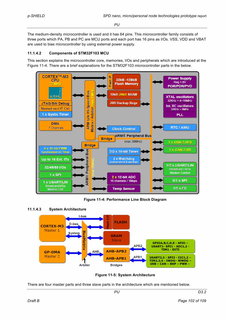
p-SHIELD SPD nano, micro/personal node technologies prototype report
PU
PU D3.2
Draft B Page 102 of 109
The medium-density microcontroller is used and it has 64 pins. This microcontroller family consists of three ports which PA, PB and PC are MCU ports and each port has 16 pins as I/Os. VSS, VDD and VBAT are used to bias microcontroller by using external power supply.
11.1.4.2 Components of STM32F103 MCU
This section explains the microcontroller core, memories, I/Os and peripherals which are introduced at the Figure 11-4. There are a brief explanations for the STM32F103 microcontroller parts in the below.
Figure 11-4: Performance Line Block Diagram
11.1.4.3 System Architecture
Figure 11-5: System Architecture
There are four master parts and three slave parts in the architecture which are mentioned below.

p-SHIELD SPD nano, micro/personal node technologies prototype report
PU
PU D3.2
Draft B Page 103 of 109
Masters:
• I-bus (Cortex-M3 ICode bus): It connects the Cortex M3 core to the Flash memory instruction in order to do perfecting.
• D-bus (DCode bus): It connects the Cortex-M3 core to the Flash memory Data interface. • S-bus (System bus): It connects the Cortex-M3 core peripheral bus to a BoxMatrix in order to
control the arbitration between the DMA and Core. • GP-DMA bus (General Purpose DMA): It connects CPU (Central Processing Unit) and DMA to
the Flash memory, SRAM and Peripherals through BoxMatrix in order to make communication between them.
Slaves:
• Internal SRAM • Internal Flash Memory • AHB (Advanced High Performance Bus) to APB (Advanced Peripheral Bus) bridge: This bridge
divides AHP bus into two buses, APB1 and APB2. APB1 is for peripheral which their frequency is 36 MHz and APB2 is for peripherals which they operate with 72 MHz frequency.
11.1.4.3.1 ARM Cortex-M3 core
Is the microcontroller CPU and is one of the most significant parts of the microcontroller. This core is the ARM processor which is applied for embedded system. It has well specifications such as 72 MHz maximum frequency, 90DIMPS (Distributed Integrated message Processing System) with 1.25 DIMPS/MHz, performance at zero state memory access, Single-cycle multiplication and hardware division, Nested interrupt controller (maskable interrupt 43 channels, Interrupt processing), Low-power consumption, Low-price, Low-gate count, etc.
11.1.4.3.2 Memory system
This microcontroller consists of two parts which they are Flash memory and SRAM (Static Random Access Memory) memory. Flash memory is for storing data and program and its capacity is up to 128 Kbytes. SRAM memory is to read/write at CPU with zero wait state in order to store data for processing by USB and its capacity is up to 20 Kbytes.
11.1.4.3.3 Nested Vect It Ctrl (NVIC)
NVIC can be used to control up to 43 maskable interrupt channels (maskable interrupt is a special interrupt which could be enabled/disabled or manage by the programmer) and, it has 16 programmable priority levels. It is used to set IRQ (Interrupt Request) channel priorities.
11.1.4.3.4 Ext. ITs (EXTI)
Stands for External Interrupt/Event Controller; it has nineteen edge detector lines in order to create interrupt/event requests. In order to detect external triggers can be used, can be trigged by rising, falling or both trigger and it is also maskable. It is possible to be connected up to eighty GPIOs to sixteen external interrupt lines to detect external triggers (as interrupts).
11.1.4.3.5 Clock system (SYSCLK)
Consists of different clock sources in the microcontroller as well as: HSI (High Speed Internal) oscillator clock, HSE (High Speed External) oscillator clock, PLL (Phase Locked Loop) clock, and LSI RC (Low Speed Internal Resistor and Capacitor oscillator) and LSE (Low Speed External) Oscillator. HSI oscillator clock is a High Speed Internal clock signal that is an internal (8 MHz) RC oscillator. It is always applied as
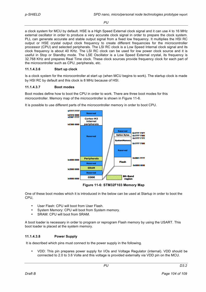
p-SHIELD SPD nano, micro/personal node technologies prototype report
PU
PU D3.2
Draft B Page 104 of 109
a clock system for MCU by default. HSE is a High Speed External clock signal and it can use 4 to 16 MHz external oscillator in order to produce a very accurate clock signal in order to prepare the clock system. PLL can generate accurate and stable output signal from a fixed low frequency. It multiplies the HSI RC output or HSE crystal output clock frequency to create different frequencies for the microcontroller processor (CPU) and selected peripherals. The LSI RC clock is a Low Speed Internal clock signal and its clock frequency is about 40 KHz. The LSI RC clock can be used for low power clock source and it is useful in Stop or Standby mode. The LSE Oscillator is a Low Speed External crystal, its frequency is 32.768 KHz and prepares Real Time clock. These clock sources provide frequency clock for each part of the microcontroller such as CPU, peripherals, etc.
11.1.4.3.6 Start up clock
Is a clock system for the microcontroller at start up (when MCU begins to work). The startup clock is made by HSI RC by default and this clock is 8 MHz because of HSI.
11.1.4.3.7 Boot modes
Boot modes define how to boot the CPU in order to work. There are three boot modes for this microcontroller. Memory map of the microcontroller is shown in Figure 11-6.
It is possible to use different parts of the microcontroller memory in order to boot CPU.
Figure 11-6: STM32F103 Memory Map
One of these boot modes which it is introduced in the below can be used at Startup in order to boot the CPU,
• User Flash: CPU will boot from User Flash. • System Memory: CPU will boot from System memory. • SRAM: CPU will boot from SRAM.
A boot loader is necessary in order to program or reprogram Flash memory by using the USART. This boot loader is placed at the system memory.
11.1.4.3.8 Power Supply
It is described which pins must connect to the power supply in the following.
• VDD: This pin prepares power supply for I/Os and Voltage Regulator (internal). VDD should be connected to 2.0 to 3.6 Volte and this voltage is provided externally via VDD pin on the MCU.

p-SHIELD SPD nano, micro/personal node technologies prototype report
PU
PU D3.2
Draft B Page 105 of 109
• VSSA, VDDA: These pins prepare external analogue power supply for ADC, Reset blocks, RCs and PLL. These pins (VSSA, VDDA) should be connected to 2.0 to 3.6 Voltage.
• VBAT: This pin prepares power supply for RTC (Real Time Clock), Internal Clock oscillator (32 KHz) and Backup registers.
This microcontroller consists of POR (Power On Reset)/PDR (Power Down Reset), it is an Integrated Circuitry and is always activated in order to fix operation starting from 2.0 Volt. When VDD is less than specific threshold (VPOR/PDR), the microcontroller cannot work and it stays on reset mood. PVD (Programmable Voltage Detector) compares VDD with VPVD threshold. The interrupt service routine informs the microcontroller or put it into safe state, if VDD voltage goes up or down VPVD (threshold voltage).
11.1.4.3.9 Direct Memory Access (DMA)
Transfers data from Memory to Memory, Memory to Peripheral and Peripheral to Memory. DMA consists of seven channels (each channel is used by the hardware which it requests DMA) and it can be applied with main peripherals such as ADC (Analogue to Digital Converter), TIMx (General Purpose and Advanced Control Timers), SPI, USART, I²C, etc.
11.1.4.3.10 Real Time Clock (RTC)
RTC and Backup registers prepares a 32 bits programmable counter for this MCU in order to provide a set of continuously running counters. They are applied for preparing a Clock Calendar function, a periodic interrupt and an alarm interrupt. Power is provided by VDD or VBAT pins for the RTC and Backup registers.
11.1.4.3.11 General Purpose Timers (TIMx)
Makes up three standard timers which are able to be synchronized in order to be applied for MCU. Each of these timers consists of 16 bits counter (auto reloadable), Pulse mode output or PWM (Pulse Width Modulation), and they also have a 16 bit prescaler and four independent channels in order to capture input/output or compare.
11.1.4.3.12 Advanced Control Timer (TIM1)
Is as the same as TIMx if it is configured as a standard 16 bits timer, but it is more complete. It can use four independent channels for Input capture, Output compare, PWM generation, etc. It also can work as a three phase PWM multiplexed on six channels.
11.1.4.3.13 Inter-Integrated Circuit (I²C)
Is a bus interface and can perform in two modes which these modes are slave and master. This microcontroller consists of up to two I²C bus interfaces.
11.1.4.3.14 Universal Synchronous / Asynchronous Receive Transmitter (USART)
Is a serial port and there are two USARTs are available. One of them can communicate up to 4.5 Mbit/S and another one is up to 2.25 Mbit/S.
11.1.4.3.15 Serial Peripheral Interface (SPI)
Is a serial port and it is able to communicate at speeds up to 18 Mbit/S. There are two SPIs are available which can use DMA controller.

p-SHIELD SPD nano, micro/personal node technologies prototype report
PU
PU D3.2
Draft B Page 106 of 109
11.1.4.3.16 Controller Area Network (CAN)
Is a standard bus which it is used to make communication between microcontrollers and devices without using any host (computer). It can transact with speed of 1 Mbit/S.
11.1.4.3.17 Universal Serial Bus (USB)
Is a serial bus which it is used in order to transact data between MCU and PC (host). There are four kinds of USB which they are grouped according their speeds.
• Low Speed: Its rate is 1.5 Mbit/S • Full Speed: Its rate is 12 Mbit/S • Hi Speed: Its rate is 480 Mbit/S • Super Speed: Its rate is 5 Gbit/S
The USB peripheral for this MCU is Full Speed version (12 Mbit/S).
11.1.4.3.18 General Purpose Input / Outputs (GPIO)
Is an interface for the MCU in order to connect it to external devices which it can use as input to read data or use as output to write data, etc. There are available three GPIOs on this MCU (STM32F103 with 80 Pins). They should be configured by software and they are significant to consider during working with the MCU. All peripherals of the MCU can connect to the outside or other external devices by GPIOs.
11.1.4.3.19 Analogue to Digital Convertor (ADC)
ADC converts a continuous input analogue signals to digit values in order to use by digital devices such as MCU, PC, etc. This electronic device receives an analogue voltage or current as an input in order to create discrete values at its output. This microcontroller has two ADCs which their resolution is 12 bits and each one has 16 channels.
11.1.5 STM32W
With these new members, the STM32 family is expanding to the wireless network domain, bringing outstanding radio and low-power microcontroller performances in a single system-on-chip (SoC). With a configurable total link budget of up to 109 dB and the efficiency of the ARM Cortex-M3 core, the
STM32W is the perfect fit for the wireless sensor network market.
Compliant with the IEEE 802.15.4 radio standard, this open and flexible platform supports the most popular protocol stacks such as RF4CE, ZigBee-PRO, 6LoWPAN and more. Coming with a complete and low-cost development tool offer, the STM32W takes full advantage of the unrivalled ST ARM Cortex-M3 portfolio.
Features:
• Outstanding 2.4 GHz radio performances to IEEE 802.15.4 • Best-in-class code density, thanks to its ARM Cortex-M3 core • Low-power architecture • Open platform with extra resources for application integration: Configurable I/Os, ADC, timers,
SPI, UART • Main software libraries: EmberZnet PRO, RF4CE, IEEE 802.15.4 MAC • Available in both SoC (QFN48) and coprocessor (QFN40) versions
p-SHIELD SPD nano, micro/personal node technologies prototype report
PU
PU D3.2
Draft B Page 107 of 109
Benefit:
• Cost efficiency through a true SoC • Open platform supporting IEEE 802.15.4 based protocol stacks • Wide STM32 Cortex-M3 developers community • Unmatched network throughput and latency • Longer battery lifetime
11.1.5.1 Components
• 32-bit ARM Cortex-M3 core running @ 24 MHz • 64 to 128-Kbyte Flash, 8-Kbyte RAM • Fully IEEE 802.15.4 compliant radio @ 2.4 GHz • Power management • Deep sleep mode <1 µA with RAM retention • On-chip debug support • ARM JTAG/SWD • Packet trace interface enables remote monitoring of radio messages • ARM memory protection unit • To detect erroneous software accesses • Sleep timer, watchdog timer and GP timers • AES-128 encryption acceleration • Serial communication (UART/SPI/I²C) • GPIO
p-SHIELD SPD nano, micro/personal node technologies prototype report
PU
PU D3.2
Draft B Page 108 of 109
12 References [1] N. Aaraj, A. Raghunathan, S. Ravi, and N. K. Jha: Energy and Execution Time Analysis of a
Software-based Trusted Platform Module, Department of Electrical Engineering, Princeton University, Princeton, NJ 08544 NEC Laboratories America, Princeton, NJ 08540, Texas Instruments R&D Center, Bangalore, India, 2007.
[2] N. Aaraj, A. Raghunathan, S. Ravi, and N. K. Jha: Analysis and design of a hardware/software trusted platform module for embedded systems, Journal ACM Transactions on Embedded Computing Systems, Volume 8 Issue 1, December 2008.
[3] M. Strasser, TPM Emulator, [Online]. Available: http://developer.berlios. de/projects/tpm-emulator.
[4] Mersenne Twister Random Numbers Generator. [Online]. Available: http://www.math.sci.hiroshima-u.ac.jp/ m-mat/MT/ewhat-is-mt.html.
[5] A. Weimerskirch, C. Paar, S. Chang Shantz: Elliptic Curve Cryptography on a Palm OS Device, V. Varadharajan and Y. Mu (Eds.): ACISP 2001, LNCS 2119, pp. 502–513, 2001, Springer-Verlag Berlin Heidelberg 2001.
[6] J. Kar, Proxy Blind Multi-signature Scheme using ECC for handheld devices, Department of Information Technology, Al Musanna College of Technology Sultanate of Oman. Available at “International Association for Cryptology Research” http://eprint.iacr.org/2011/043.pdf, 2011.
[7] D. M. Alghazzawi, T. M. Salim and S. H. Hasan, A New Proxy Blind Signature Scheme based on ECDLP, IJCSI International Journal of Computer Science Issues, Vol. 8, Issue 3, No. 1, May 2011, ISSN (Online): 1694-0814.
[8] C. Gebotys, S. Ho, A. Ti, EM Analysis of Rijndael and ECC on a PDA, Dept of Electrical and Computer Engineering, University of Waterloo Waterloo, Canada, 2005.
[9] F. Wen, X. Li, S. Cui, Cross-realm Client-to-client Password-based Authenticated Key Agreement Protocol for Mobile Devices on Elliptic Curve Cryptosystem, Journal of Convergence Information Technology, Volume 6, Number 5. May 2011.
[10] W. Chou and Laerence, Elliptic curve cryptography and its applications to mobile device, Project Report, University of Maryland, 2003, http://www.cs.umd.edu/Honors/reports/ECCpaper.pdf
[11] M. Hutter, M. Joye, and Y. Sierra, Memory-Constrained Implementations of Elliptic Curve Cryptography in Co-Z Coordinate Representation, Published in A. Nitaj and D. Pointcheval, Ed., Progress in Cryptology, AFRICACRYPT 2011, vol. 6737 of Lecture Notes in Computer Science, pp. 170-187, Springer, 2011.
[12] D. F. Aranha, R. Dahab, J. Lopez and L. B. Oliveira, Efficient Implementation Of Elliptic Curve Cryptography In Wireless Sensors, Advances in Mathematics of Communications, Volume 4, No. 2, 2010, xxx–xxx.
[13] P. L. Montgomery. Speeding up the Pollard and elliptic curve methods of factorization. Mathematics of Computation, 48(177):243-264, 1987.
[14] N. Meloni. New point addition formul_ for ECC applications. In C. Carlet and B. Sunar, editors, Arithmetic of Finite Fields (WAIFI 2007), volume 4547 of Lecture Notes in Computer Science, pages 189-201. Springer-Verlag, 2007.
[15] R. R. Goundar, M. Joye, and A. Miyaji. Co-Z addition formula and binary ladders. In S. Mangard and F.-X. Standaert, editors, Cryptographic Hardware and Embedded Systems, CHES 2010, volume 2523 of Lecture Notes in Computer Science, pages 65-79. Springer-Verlag, 2010.
[16] D.Chaum, Blind Signature for Untraceable Payments, In Crypto 82, New York, Plenum Press, pp.199-203, 1983.
[17] Dr. B. Gladman, A Specification for Rijndael, the AES Algorithm, at fp.gladman.plus.com/cryptography_technology/ rijndael/aes.spec.311.pdf, 2003.
p-SHIELD SPD nano, micro/personal node technologies prototype report
PU
PU D3.2
Draft B Page 109 of 109
[18] J.W. Byun, I.R. Jeong, D.H. Lee and C.S. Park, Password-authenticated key exchange between clients with different password, in Proc. ICICS , pp. 134-146, 2002.
[19] J.W. Byun, D.H. Lee and J.I. Lim, EC2C-PAKE:An efficient client-to-client password-authenticated key agreement, Information Science,vol 177,no.19, pp. 3995-4013, 2007.
[20] D.G. Feng and J. Xu, A new client-to-client password-authenticated key agreement protocol, in Proc. IWCC 2009, pp. 63-76,2009.
[21] W. Jin and J. Xu, An efficient and provably secure cross-realm client-to-client password-authenticated key agreement protocol with smart cards, in Proc. CANS 2009, pp. 299-314, 2009.
[22] H.S. Rhee, J.O. Kwon and D.H. Lee, A remote user authentication scheme without using smart cards, Computers Standards & Interfaces ,vol.31,no.1, pp. 6-13,2009.
[23] M.K. Khan and J. Zhang, Improving the security of a flexible biometrics remote user authentication scheme, Computer Standards & Interfaces,vol. 29 ,no.1, pp. 82-85, 2007.
[24] J.H. Yang and C.C. Chang, An ID-based remote mutual authentication with key agreement scheme for mobile devices on elliptic curve cryptosystem, Computers & Security,vol.28 no.3-4, pp. 138-143,2009.
[25] H.S. Rhee, J.O. Kwon and D.H. Lee, A remote user authentication scheme without using smart cards, Computers Standards & Interfaces ,vol.31,no.1, pp. 6-13,2009.
[26] N. Howgrave-Graham, J. H. Silverman, W. Whyte, Choosing Parameter Sets for NTRUEncrypt with NAEP and SVES-3, NTRU Cryptosystems, 2005.
[27] S. Alam, M.M.R. Chowdhury, and J. Noll, Interoperability of Security-Enabled Internet of Things, Wireless Personal Communications, Springer, vol. 61, pp. 567-586, 2011.