Embed Size (px)
Citation preview

Special MRAM poster session
IEDM (3-5 Dec 2018, San-Francisco)
Wednesday afternoon 5 Dec, 2:00pm-5:00pm
Plaza room For the 3rd consecutive year, a special poster session entirely dedicated to MRAM is organized during IEDM. This session is technically organized by the IEEE Magnetics Society and is embedded in the IEDM 2018 conference. This event will be a great opportunity to foster closer interactions between the microelectronics and magnetism communities. The posters will cover topics including MRAM materials, phenomena, technology (STT, SOT, E-field control), testing, hybrid CMOS/MTJ technology and circuits, and MRAM applications. This year, 32 posters were accepted for presentation.
The list is shown below.
Bernard DIENY and Bruce TERRIS IEEE Magnetics Society
Presented posters :
1. High-thermal-tolerance reference layer with tungsten spacer layer for perpendicular-anisotropy MTJs H. Honjo1,7, S. Ikeda1,2,4,5,7, H. Sato1,2,3,4, M. Yasuhira1,7, and T. Endoh1,2,4,5,7
1Center for Innovative Integrated Electronic Systems, Tohoku University, Sendai, Japan, 2Center for Spintronics Integrated Systems, Tohoku University, 3Laboratory for Nanoelectronics and Spintronics, RIEC, Tohoku University, 4Center for Spintronics Research Network, Tohoku University, 5Graduate School of Engineering, Tohoku University, 6WPI-Advanced Institute for Materials Research (WPI-AIMR), Tohoku University, 7JST-ACCEL
CoFeB/MgO-based magnetic tunnel junctions that using interfacial perpendicular magnetic anisotropy (p-MTJs) [1-3] are essential for high-performance STT-MRAM. To reduce the stray field of the reference layer, a synthetic ferrimagnetic (SyF) reference layer with the structure [Co/Pt] n/Co/Ru/ [Co/Pt] m/Co/ (W or Ta)/CoFeB has been employed [4-6]. In this SyF reference layer, the W or Ta layer plays the role for coupling the Co/Pt multilayer with the CoFeB layer. The SyF reference layer should be capable to withstand annealing at 400°C, which is required for standard CMOS back-end-of-line process. Although we have reported the effect of W sputtering gas species on the free layer [7], that of the gas species on the SyF reference layer remains unclear. In this work, we investigated the effects of the W deposition condition on the perpendicular magnetic anisotropy (PMA) of the reference layer and the TMR properties. We found that the PMA of the reference layer and TMR properties after annealing at 400°C are significantly improved by using Kr sputtering gas for W deposition. An EDX line analysis reveals that the diffusion of Pt towards the CoFeB reference layer after annealing at 400°C was significantly suppressed by using the Kr sputtering gas for W deposition, resulting in the reference layer exhibiting high thermal tolerance.
This work is supported by CIES’s Industrial Affiliation on STT MRAM program, JST-OPERA, and JST-ACCEL Grant Number JPMJAC1301, Japan. References [1] S. Ikeda et al., Nature Mater. 9, 721 (2010). [2] H. Sato et al., Appl. Phys. Lett. 99, 042501 (2011). [3] H. Sato et al., IEEE Trans. Mag. 49, 4437 (2013). [4] H. Sato et al., Jpn. J. Appl. Phys. 53, 04EM02 (2014). [5] K. Yakushiji et al., Appl. Phys. Exp. 8, 083003 (2015). [6] H. Honjo et al., AIP advances, 7, 055913 (2017). [7] H. Honjo et al., IEEE. Trans. Mag., to be published.
2. Capping Layer Material Dependence of Magnetic Properties of Free Layer in Perpendicularly Magnetized Magnetic Tunnel Junctions H. Tomita1,3, K. Nakamura1, Y. Tanaka1,3, K. Nagasaka1,3, K. Ando2, S. Bosu1,3, A. Gomi1, A. Fukushima3, H. Kubota3, K. Yakushiji3, S. Yuasa3, H. Maehara2,3 and N. Watanabe1
1Tokyo Electron Technology Solutions Limited 2Tokyo Electron Limited 3National Institute of Advanced Industrial Science and Technology (AIST), Spintronics Research Center2 E-mail:[email protected]
Perpendicularly magnetized magnetic tunnel junctions (p-MTJs) with a large MR ratio is required for STT-MRAM applications. Moreover, magnetic characteristics of p-MTJs (e.g., perpendicular magnetic anisotropy of free layer and strength of exchange coupling in SAF structure) are also indispensable for the stable read and write operations. In this study, we systematically investigated the effect of capping layer material on magnetic and STT-switching properties in double MgO based p-MTJ films. Various metal layers were inserted between MgO capping layer and top Ta layer. The p-MTJ films were prepared using Tokyo Electron EXIM™ sputtering system and patterned into nano-pillar MTJ devices. Our results show that the magnetic properties of the free layer are improved by inserting Ru or Mo layer. That is attributed to suppression of the Ta diffusion into the MgO capping layer. More detailed results will be discussed in the poster.
3. Magnetic Tunnel Junctions with MgO Tunnel Barrier Formed by Post-Oxidation Process for STT-MRAM H. Tomita1,3, K. Nakamura1, Y. Tanaka1,3, K. Nagasaka1,3, K. Ando2, S. Bosu1,3, A. Gomi1, A. Fukushima3, H. Kubota3, K. Yakushiji3, S. Yuasa3, H. Maehara2,3, and N. Watanabe1
1Tokyo Electron Technology Solutions Limited 2Tokyo Electron Limited
3National Institute of Advanced Industrial Science and Technology (AIST), Spintronics Research Center E-mail: [email protected]
Magnetic random access memory using spin-transfer-torque switching (STT-MRAM), whose memory cells are consisting of MgO tunnel barrier based magnetic tunnel junctions (MTJs), is intensively researched and developed as a new non-volatile memory. To realize STT-MRAM as a commercial application, we must develop the manufacturing technologies for MTJ cells with considering cost and yield keeping the performance, because STT-MRAM performances (operation speed, density and retention etc.) strongly depend on the MTJ characteristics. Especially, quality control of crystallinity and stoichiometry in an MgO tunnel barrier layer in the MTJ is crucially important. In general, there are two methods of MgO tunnel barrier layer formation; one is RF sputtering using sintered an MgO target and another is post oxidation process for deposited metal Mg layer. We compared the magnetic and electrical performances of the two types MTJs, which were fabricated by the two methods, and obtained the same results. This results indicate that the optimized post oxidation process can obtain high quality MgO tunnel barrier. We conclude that the post oxidation process is suitable for high volume manufacturing due to good productivity. We will describe the details of feature of our post oxidation process and evaluated results.

4. Enhancing magnetic materials at the atomic scale using light ion irradiation L. Herrera Diez1, M.Sall1, M.Belmeguenai2, Y.Roussigné2, A.Stashkevich2, S.M. Cherif2, G.Durin3, Arianna casiraghi3, M. Voto4, L. Lopez-Diaz4, J.Langer5, B. Ocker5 and D. Ravelosona1,6 1 Centre de Nanosciences et de Nanotechnologies, CNRS, Univ. Paris-Sud, Université Paris-Saclay, C2N – Orsay, 91405 Orsay cedex, France. 2LSPM (CNRS-UPR 3407), Université Paris 13, Sorbonne Paris Cité, 99 avenue Jean-Baptiste Clément,93430 Villetaneuse, France 3Istituto Nazionale di Ricerca Metrologica, Turin, Italy 4Departamento Fisica Aplicada, Universidad de Salamanca, plaza de los Caidos s/n E-38008, Salamanca, Spain 5Singulus Technology AG, Hanauer Landstrasse 103, 63796 Kahl am Main, Germany. 6Spin-Ion Technologies, 91405 Orsay France
Materials with perpendicular magnetic anisotropy (PMA) are considered as the most promising candidates for the next generation of ultra-high density Magnetic Random Access Memory (MRAM) devices. One crucial issue for MRAM technologies is to better understand and minimize the role played by structural inhomogeneties that induce a distribution of magnetic properties and stochastic behaviour.
One elegant approach to adress this issue is to use light He ion irradiation that has demonstrated to be extremely efficient in controlling at the atomic scale the magnetic properties of magnetic thin films and multilayers [1-4] since only interatomic displacements are induced with no cascade collisions and surface sputtering. We have investigated the effect of He ion irradiation on the structural and magnetic properties of CoFeB-MgO ultra-thin films with PMA, which are considered as the best materials for MRAM applications. For that, we have developped a very compact He ion irradiation facility that allows us to irradiate thin films at energies 5-30 keV and temperatures up to 500°C. This advanced tool can be easily integrated with an UHV deposition system [5], enabling the in-situ optimization of magnetic layers.
In this poster, we will show three important results that suggest a pathway to optimize MRAM devices using He ion irradiation : (1) crystallization of (Ta or W)- CoFeB-MgO layer can be obtained at much lower temperatures than pure annealling with sharper interfaces and texture, (2) engineering smoothly interface by irradiation allows us to increase domain wall velocities and Dzyaloshinskii-Moriya Interaction in magnetic nanowires and (3) using irradiation through a mask, local modulation of magnetic anisotropy can bring new functionalities for future spintronic nanodevices involving Skyrmions and Spin Orbit Torques.
REFERENCES
[1] J.Fassbender , D.Ravelosona, Y.Samson., J.Phys.D: Appl. Phys. 37, 179 (2004). [2] T.Devolder et al, Jour. Appl. Phys. 113, 203912 (2013) [3] L.Herrera Diez et al, Appl. Phys. Lett 107, 032401 (2015) [4] D.Ravelosona et al, Magnetic Nano- and Microwires, Elsevier (2015) [5] www.spin-ion.com 5. Correlation between interfacial Dzyaloshinskii-Moriya interaction and interfacial magnetic anisotropy in Pt/Co/MgO structures Woo-Yeong Kim1, 2, Hyung Keun Gweon1, Sang Ho Lim1, Kyung-Jin Lee1, 3*, and Chun-Yeol You2†
1Department of Materials Science and Engineering, Korea University, Seoul 02841, Korea 2Emerging Materials Science, Daegu Gyeongbuk Institute of Science & Technology, Daegu 42988, Korea. 3KU-KIST Graduate School of Converging Science and Technology, Korea University, Seoul 02841, Korea Corresponding author: *[email protected], †[email protected] Interfacial magnetic energies such as interfacial Dzyaloshinskii-Moriya interaction (iDMI) and interfacial perpendicular magnetic anisotropy (iPMA) are decisive for the performance of magnetic

devices consisting of thin-film heterostructures. From the application point of view, it is important to investigate a possible correlation between iDMI and iPMA because different applications require different values of iDMI and iPMA. For example, chiral domain wall or skyrmion dynamics requires a large iDMI and large iPMA, whereas for STT-MRAM application, a large PMA with a negligible iDMI is preferred. In this respect, it is of crucial importance to understand the correlation between interfacial magnetic energies. We experimentally investigate the correlation between iDMI and iPMA for Pt/Co/MgO stacks, with varying the annealing temperature. We find that the iDMI of whole stack decreases with increasing the iPMA. Assuming that the interfacial magnetic energies of whole stack are the sum of separate contributions from the Pt/Co and Co/MgO interfaces, the observed negative correlation between the two interfacial energies of Pt/Co/MgO structures is found to originate from different correlations between iDMI and iPMA at the two interfaces. Our result suggests a possibility to design the interfacial magnetic energies of whole stack by controlling the contributions of each interface respectively. 6. Ultra-thin polycrystalline Co25Fe75 films for perpendicular magnetic tunnel junctions Ikhtiar, Xueti Tang, Sebastian Schafer, and Mohamad Krounbi Samsung Semiconductor Inc., New Memory Technology Lab, San Jose, CA, 95134, USA [email protected]
The perpendicular magnetic tunnel junction is a critical building block for realizing STT-MRAM cells with low power consumption and sufficiently long data retention [1]. The ultra-thin CoFeB layer, in combination with polycrystalline MgO barrier, has been widely used in p-MTJ due to its practical advantages, such as high TMR ratio and strong perpendicular anisotropy [1]. In the widely adopted free layer structure, i.e. double-oxide-interface free layers [2,3,4], the control of Boron diffusion is very critical as it dictates the CoFeB crystallization into CoFe hence affecting the corresponding TMR ratio and perpendicular magnetic anisotropy.
Here, the ultra-thin Co25Fe75 film is studied as a free layer with double-oxide-interface structure. The absence of Boron in the as-deposited free layer might eliminate the issue with Boron diffusion, hence simplifying free layer structure. Double-oxide-interface free layer stacks of underlayer/MgO(~10Å)/ CoFe(11-19 Å)/MgO(~8 Å)/cap were deposited on 12” Si wafer with oxidized surface by physical vapor deposition sputtering tools. The stacks were then post-annealed at 400˚C for 30 minutes with external magnetic field of 3 Tesla. The broadband ferromagnetic resonance and vibrating sample magnetometer were performed at room temperature. Detailed magnetic properties of the ultra-thin Co25Fe75 film and its potential for perpendicular magnetic tunnel junctions will be discussed in this presentation.
REFERENCES
[1] S. Ikeda et al., “A perpendicular-anisotropy CoFeB-MgO magnetic tunnel junction”, Nature Mater., 9, 721 (2010).
[2] H. Kubota et al., “Enhancement of perpendicular magnetic anisotropy in FeB free layers using a thin MgO cap layer”, J. Appl. Phys., 111, 07C723 (2012).
[3]J-H..Park et al., “Enhancement of data retention and write current scaling for sub-20nm STT-MRAM by utilizing dual interfaces for perpendicular magnetic anisotropy”, Dig. Tech. Pap. – Symp. VLSI Technol., 721, 57 (2012).
[4] H. Sato et al., “Perpendicular-anisotropy CoFeB-MgO magnetic tunnel junction with MgO/CoFeB/Ta/ CoFeB/ MgO recording structure”, Appl. Phys. Lett., 101, 022414 (2012).
7. Effects of RIE on the properties of Ta/CoFeB/MgO/Ta film stack Yao-Jen Chang1, Shan-Yi Yang1, Yu-Chen Hsin1, Jeng-Hua Wei1, Keh-Ching Huang1, Chih-I Wu1, Zhao-wen Chen2, Yeo-yu Cheng2, Lin-Xiu Ye2, Duan-li Deng1,2, Te-ho Wu2* 1EOSL, ITRI, Hsinchu, Taiwan, ROC 2 Graduate School of Materials Science, National Yunlin University of Science and Technology, Yunlin, Taiwan;
*Corresponding author: Te-ho Wu, [email protected]
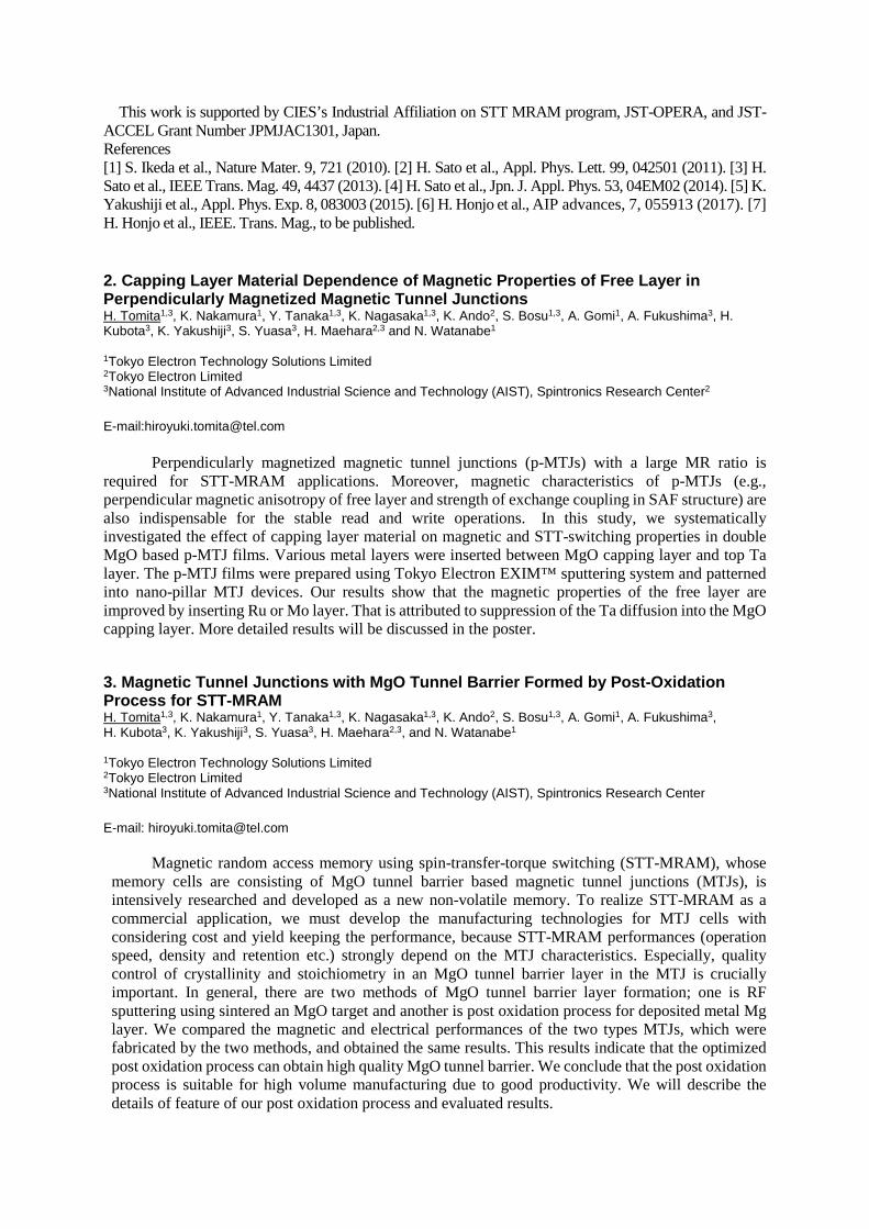
It has been shown that during MTJ processing, the high energy ion of RIE can induce penetrating damages to the ferromagnetic layers underneath MgO surface where the etch stops [1, 2]. MRAM industry has been trying both the reactive RIE and non-reactive IBE for high density MRAM patterning to eliminate such etch damage. This paper presents a study of the etch damage by comparing the post etch film of different etch conditions. We find the etch condition makes a big difference. Two sets of film stacks are prepared (Fig.1), one with CoFeB wedge and the other Ta seeding wedge. Each stack is etched with two different RIE conditions (A-Etch, B-Etch). A-Etch is designed for STT MRAM and B-Etch is designed for SOT MRAM. Among few differences in etching properties, A-Etch etches Ta very fast, and MgO very slowly, while the etching rate of B-Etch is opposite. We observe that A-Etch induces substantial reduction in magnetization Ms of CoFeB even though the MgO on top is not etched away, while the B-Etch virtually does nothing to the Ms (Fig.2.a). One may infer the Ms reduction as a result of the formation of magnetic dead-layer. Same test on Stack-2 allows one to derive the dead-layer thickness of A-Etch to be 0.35nm, and B-Etch ~0nm. (Fig.2.b) In addition, two RIEs also alter the effective anisotropy of the stack film differently. We will show the details. References: [1] C.W. Chien, et.al, IEEE ELECTRON DEVICE LETTERS, VOL. 34, NO. 2, p.241, FEBRUARY (2013). [2] T. Mukai et.al, Japanese Journal of Applied Physics, Volume 45, Part 1, Number 6B, (2006)
8. Low Energy Ion Beam Trimming Step in MTJ patterning Shuogang Huang, Weiyi Li, Zhimin Wan, Seokmin Yun, Ivan (Skip) Berry, Konstantin Smekalin Lam Research, 4650 Cushing Parkway, Fremont CA 94538 With MRAM quickly gaining acceptance as the next generation embedded memory in IoT devices, MTJ patterning development focuses on achieving high TMR, and ultra-low electrical short density as the necessary conditions for successfully transferring MRAM to volume production. These two objectives can only be achieved if by the end of the patterning process, the MTJ sidewalls are free of metallic deposits, and have minimal structural and compositional damage. For the Ion Beam Etching (IBE) process, which is an established approach for MTJ patterning, producing deposits- and damage-free MTJ sidewalls is a major challenge because the high voltage ion beam used for delineating the MTJ structures also sputters metals back onto the freshly defined MTJ sidewalls. An alternative is to use a two-step process: the high energy (~1000 eV) beam step for high overall process throughput, followed by the low energy (≤ 100 eV) beam step to remove the sidewall deposits and damage layer. This work

studies the low-energy beam process step in detail, investigating the relationship between process parameters (ion beam energy, ion beam atom, wafer-to-beam tilt angle, process time) and the MTJ sidewall properties. We used simulation to demonstrate how a properly designed low energy beam process leads to sufficiently deposits-free and damage-free MTJ sidewall. 9. A Patterning Solution by Utilizing Combined Etching for STT-MRAM Kaidong Xu1,2, Dongdong Hu1, Dongchen Che1, Hongyue Sun1, Mikhail R. Baklanov1, Jiale Tang2, Shiwei Zhuang2, Lu Chen1
1 Leuven Instruments Co. Ltd (Jiangsu), Pizhou, Jiangsu, China 2 Jiangsu Normal Univeristy, Xuzhou, Jiangsu, China Email: [email protected]
In STT-MRAM devices, the magnetic tunnel junction (MTJ), which is composed with ferromagnetic layer, dielectric tunneling barrier layer and ferromagnetic layer, is the critical factor for performance. In order to obtain good performance STT-MRAM with small scale, processing MTJ stacks requires specially developed nano-patterning solution. However, it is still very much a laborious process for STT-MRAM to replace conventional dense-array memories, because MTJ stack materials, such as MgO, CoFeB, and CoPt, cannot easily form volatile compounds in the temperature of standard etching chamber by conventional etch process. In industry, both reactive ion etch (RIE) and ion beam etch (IBE) processes were under research to overcome the MTJ etch bottleneck. Although both of them work for relatively isolated and large devices, none of them works for sub-30nm dense array structures.
In this paper, the combination of reactive ion etch (RIE) and ion beam etch (IBE) process was utilized for the patterning of perpendicular MTJ stacks. RIE offers high plasma density, high etch rates, and high selectivity. RIE allows the fast definition of required patterning profiles at small CD and relatively high aspect ratio and it also enables a flat etch front, which is needed for sub-30nm dense-array devices. On the other hand, RIE has relatively broad ion energy distribution, some portions of which tend to cause MTJ sidewall damage. IBE has relatively tighter distribution of ion energy. By controlling the ion energy and the beam incident angle, MTJ sidewall damage is more easily restricted. In this work, a RIE etch is utilized as a main etch to define the pattern, followed by an IBE etch and post-etch process to control the sidewall re-deposition and the sidewall damage. Furthermore, an in-situ deposition of dielectric layer protects the MTJ cells prior to the exposure of MTJ to the ambient. All processes were performed under the same processing cluster, without vacuum break in between. Sub-30nm MTJ devices was demonstrated to be well patterned, without sidewall re-deposition, with minimum sidewall damage, and leaving a flat etch front. By using a proper hard mask strategy, a new patterning approach / apparatus is introduced, which is believe to be the patterning vehicle for STT-MRAM for DRAM replacement applications. 10. Numerical Demonstration of Multi-functional MRAM Cell Based on Inertial Magnetic Switching Xiaoguang Li1, and Yan Zhou1
1School of Science and Engineering, Chinese University of Hong Kong, Shenzhen 518172, China [email protected]
Efficient mechanism for reorienting magnetization is the key to high performance magnetic random-access memory (MRAM). In recent years, current induced spin-orbit torque (SOT) in heavy metal (HM)/ferromagnet (FM) heterostructure has been intensively investigated due to its potential applications in the three-terminal MRAM and other spintronic devices. Compared with the current STT based scheme, SOT leads to a better writing efficiency. More importantly, the reading and writing performance can be independently optimized to solve the dilemma caused by tunneling barrier breakdown and reading disturbance. Unfortunately, the memory cell with perpendicular magnetic
anisotropy requires a finite magnetic bias field to achieve reliable magnetization switching, forming the main barricade on its road towards CMOS applications. In our poster, we would like to present the numerical demonstration of a novel spin inertia-based memory cell, which is capable of all-electrical switching of perpendicular MTJ (pMTJ) through SOT. The functioning part of the memory cell is composed of pMTJ, HM layer and FM underlayer, in which the HM layer serves as both the interlayer exchange spacer and the spin Hall channel. The magnetization switching of pMTJ is free from incubation since the spin polarization direction is orthogonal to the easy axis of the free layer. Further, numerical results show that the switching process can be accelerated by antiferromagnetic coupling between the ferromagnetic layers, leading to reliable switching within several tens of picoseconds, which is an order faster than the current scheme. More importantly, various switching modes, including deterministic switching, stochastic switching and precessional switching can be realized with different current pulse configurations, shedding light on a multi-functional unit. More details, including the phase change of switching behavior and the composite properties influences on it, will be presented in our poster. 11. Micromagnetic modeling of non-uniformities in magnetic tunnel junctions for MRAM Devices Volvach I.1, Marko V. Lubarda1 and Vitaliy Lomakin1
1ECE Department University of California, San Diego
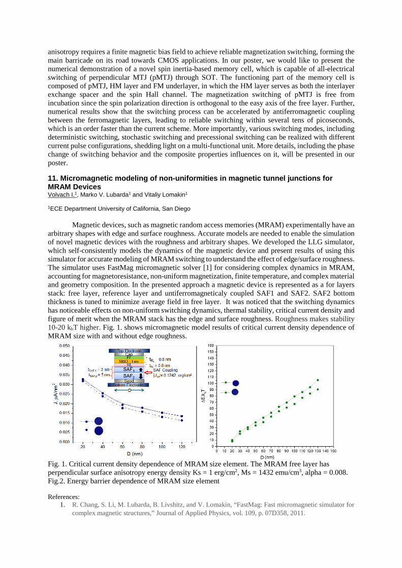
Magnetic devices, such as magnetic random access memories (MRAM) experimentally have an arbitrary shapes with edge and surface roughness. Accurate models are needed to enable the simulation of novel magnetic devices with the roughness and arbitrary shapes. We developed the LLG simulator, which self-consistently models the dynamics of the magnetic device and present results of using this simulator for accurate modeling of MRAM switching to understand the effect of edge/surface roughness. The simulator uses FastMag micromagnetic solver [1] for considering complex dynamics in MRAM, accounting for magnetoresistance, non-uniform magnetization, finite temperature, and complex material and geometry composition. In the presented approach a magnetic device is represented as a for layers stack: free layer, reference layer and untiferromagneticaly coupled SAF1 and SAF2. SAF2 bottom thickness is tuned to minimize average field in free layer. It was noticed that the switching dynamics has noticeable effects on non-uniform switching dynamics, thermal stability, critical current density and figure of merit when the MRAM stack has the edge and surface roughness. Roughness makes stability 10-20 kbT higher. Fig. 1. shows micromagnetic model results of critical current density dependence of MRAM size with and without edge roughness.
Fig. 1. Critical current density dependence of MRAM size element. The MRAM free layer has perpendicular surface anisotropy energy density Ks = 1 erg/cm2, Ms = 1432 emu/cm3, alpha = 0.008. Fig.2. Energy barrier dependence of MRAM size element References:
1. R. Chang, S. Li, M. Lubarda, B. Livshitz, and V. Lomakin, “FastMag: Fast micromagnetic simulator for complex magnetic structures,” Journal of Applied Physics, vol. 109, p. 07D358, 2011.

12. From conventional STT-MRAM to Perpendicular Shape Anisotropy STT-MRAM (PSA-STT-MRAM): Dramatic reduction in temperature variation of anisotropy N.Perrissin, G.Gregoire, S.Lequeux, L. Tille, N.Strelkov, A.Chavent, S. Auffret, L.Buda-Prejbeanu, R. Sousa, L. Vila, I.L. Prejbeanu and B. Dieny Univ. Grenoble Alpes, CEA, CNRS, Grenoble INP, INAC-Spintec, 38000 Grenoble, France email: [email protected]
Recently, the concept of Perpendicular Shape Anisotropy STT-MRAM (PSA-STT-MRAM) has been independently proposed by SPINTEC and Tohoku University. It consists in significantly increasing the thickness of the storage layer in STT-MRAM to values comparable to the cell diameter so as to induce a perpendicular shape anisotropy in this layer which comes on top of the MgO/FeCoB interfacial anisotropy (iPMA). Thanks to this robust source of bulk anisotropy, PSA-STT-MRAM offers a much improved downsize scalability than conventional perpendicular STT-MRAM. Despite the large thickness of the storage layer, PSA-STT-MRAM cells can still be written by spin transfer torque provided their thermal stability factor ∆ is adjusted in the same range as in conventional STT-MRAM i.e. ∆ of the order of 60 to 100 depending on the memory capacity and required bit error rate. We show in this paper that thermally stable PSA-STT-MRAM cells of diameter down to 5nm were fabricated and characterized. In addition, thanks to the increased thickness of the storage layer, the magnetic properties of the storage layer and in particular its temperature dependence of magnetization are much closer to those of the corresponding bulk material than in conventional STT-MRAM where the storage layer is only 1nm to 2nm thick. As a result, the magnetic anisotropy and therefore the memory retention are much less sensitive on temperature than in conventional STT-MRAM. For instance, on the range of temperature 300k-390K, the anisotropy of PSA-STT-MRAM varies by 5% to 10% whereas that of conventional STT-MRAM varies by ~40%. This is very interesting for applications operating on a wide range of temperatures (e.g.automotive -40°C - +150°C) as well as to fulfill solder reflow compliance. This study was funded by ERC Adv grant MAGICAL n°664209.
Fig.1: Comparison of the thermal variation of the coercive field, for conventional STT-MRAM based on iPMA and for PSA-STT-MRAM of various compositions. The storage layer has the form FeCoB(1,4)/W(2)/M tM/Ta where M is either Co or NiFe as indicated in the figure. The cell diameters were in the range 10 to 20nm. Fig.2: Corresponding comparison of the thermal variation of the TMR.
13. STT efficiency modulation in double barrier pSTT-MRAM cell with read/write mode control layer P.Coehlo, J.Chatterjee, A.Chavent, N.Strelkov, S. Auffret, L.Buda-Prejbeanu, R. Sousa, L. Vila, M.Chshiev, I.L. Prejbeanu, B.Dieny and C.Baraduc Univ. Grenoble Alpes, CEA, CNRS, Grenoble INP, INAC-Spintec, 38000 Grenoble, France email: [email protected]
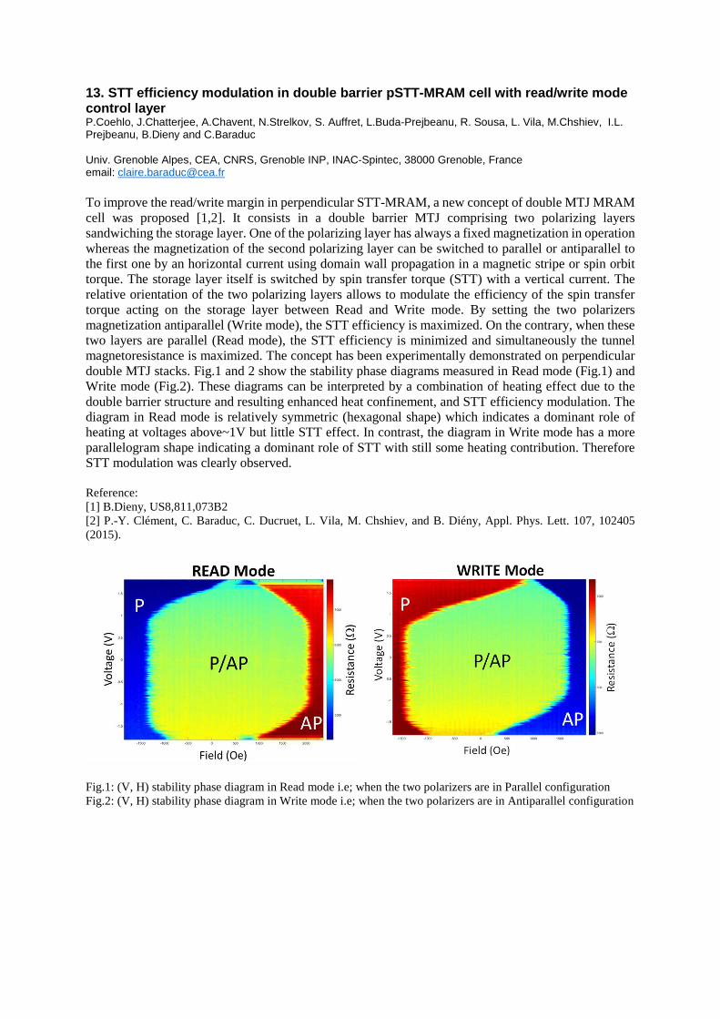
To improve the read/write margin in perpendicular STT-MRAM, a new concept of double MTJ MRAM cell was proposed [1,2]. It consists in a double barrier MTJ comprising two polarizing layers sandwiching the storage layer. One of the polarizing layer has always a fixed magnetization in operation whereas the magnetization of the second polarizing layer can be switched to parallel or antiparallel to the first one by an horizontal current using domain wall propagation in a magnetic stripe or spin orbit torque. The storage layer itself is switched by spin transfer torque (STT) with a vertical current. The relative orientation of the two polarizing layers allows to modulate the efficiency of the spin transfer torque acting on the storage layer between Read and Write mode. By setting the two polarizers magnetization antiparallel (Write mode), the STT efficiency is maximized. On the contrary, when these two layers are parallel (Read mode), the STT efficiency is minimized and simultaneously the tunnel magnetoresistance is maximized. The concept has been experimentally demonstrated on perpendicular double MTJ stacks. Fig.1 and 2 show the stability phase diagrams measured in Read mode (Fig.1) and Write mode (Fig.2). These diagrams can be interpreted by a combination of heating effect due to the double barrier structure and resulting enhanced heat confinement, and STT efficiency modulation. The diagram in Read mode is relatively symmetric (hexagonal shape) which indicates a dominant role of heating at voltages above~1V but little STT effect. In contrast, the diagram in Write mode has a more parallelogram shape indicating a dominant role of STT with still some heating contribution. Therefore STT modulation was clearly observed. Reference: [1] B.Dieny, US8,811,073B2 [2] P.-Y. Clément, C. Baraduc, C. Ducruet, L. Vila, M. Chshiev, and B. Diény, Appl. Phys. Lett. 107, 102405 (2015).
Fig.1: (V, H) stability phase diagram in Read mode i.e; when the two polarizers are in Parallel configuration Fig.2: (V, H) stability phase diagram in Write mode i.e; when the two polarizers are in Antiparallel configuration

14. Multi-bit MRAM storage cells utilizing serially connected perpendicular magnetic tunnel junctions Piotr Rzeszut1, Witold Skowroński1, Sławomir Ziętek1, Jerzy Wrona2 and T. Stobiecki 1,3
1 AGH University of Science and Technology, Department of Electronics, 30-059 Kraków, Poland 2 Singulus technologies, Kahl am Main, 63796, Germany 3 AGH University of Science and Technology, Faculty of Physics and Applied Computer Science, 30-059 Kraków, Poland
One of the main limitation of the storage density of a contemporary MRAM cell is the size of the transistor capable of driving sufficiently high current density needed to switch magnetic tunnel junctions (MTJ). This limitation can be overcome by using so-called multi-bit MRAM cell; however, to date, only a few practical implementations have been presented [1-3]. This is mainly due to the fact, that efforts were made to produce a single storage element capable of being stable in more than two states, or to produce multiple storage elements on the top of each other.
Here, an alternative solution is presented - the multi-bit cell is based on a perpendicular MTJ consisting of the following layer structure: buffer / SAF / 1 CoFeB / 0.89 MgO / 1.3 FeCoB / 0.3 W / 0.5 FeCoB / capping, where SAF is Co-Pt-Ru-based synthetic antiferromagnet and top CoFeB / W / CoFeB is a composite free layer [4], patterned into circular pillars of around 100 nm diameter. MTJs are connected electrically in series, as shown in Fig. 1 The cell writing process is based on spin transfer torque effect; starting from parallel state of all MTJs (‘00’), increasing a positive bias voltage induces switching of subsequent MTJs to antiparallel leading to the cell resistance change. Resetting the cell to the ‘00’ state is realized by applying sufficient negative bias – Fig. 2.
The developed method of manufacturing and driving multi-bit non-volatile storage allows to store more data using the same driving transistor area. The proof-of-concept is verified experimentally in three-bit cell, consisting of seven MTJs, however the method will also work with more elements involved. Acknowledgements: This work is supported by the Polish Ministry of Science and Higher Education Diamond Grant No. 0048/DIA/2017/46 and the Polish National Center for Research and Development grant No. LIDER/467/L-6/14/NCBR/2015. T.S. acknowledges from Statutory Grant Faculty of Physics and Applied Computer Science 11.11.220.01. References [1] Jeong, W. et al. J. Appl. Phys. 85.8 (1999): 4782. [2] Ju, K., and Oletta, A.. IEEE Trans. Mag. 42.10 (2006): 2730. [3] Zhang, D. et al. Trans. Biomed. Circuits Syst. 10.4 (2016): 828 [4] Skowroński, W. et al. Sci. Rep. 7.1 (2017): 10172.
15. Multifunctional magnetic tunnel junction standardized stack as universal spintronic technology for IoT A. Chavent1, V. Iurchuk1, L.Tillie1, Y. Bel1, L. Vila1, U. Ebels1 R. Sousa1 B. Dieny1, G. di Pendina1, G. Prenat, J. Langer2, J. Wrona2, I. L. Prejbeanu1
1 Univ. Grenoble Alpes, CEA, CNRS, Grenoble INP*, INAC-Spintec, 38000 Grenoble, France * Institute of Engineering Univ. Grenoble Alpes2Laboratory on GRMN 2 Singulus Technologies AG, 63796 Kahl am Main, Germany
For monolithic heterogeneous integration, fast yet low-power processing and storage, and high integration density, the objective of this study is to co-integrate multiple digital and analog functions together within CMOS by adapting the Magnetic Tunneling Junctions (MTJs) into a single baseline technology enabling logic, memory, and analog functions, particularly for Internet of Things (IoT) platforms. This will lead to a unique STT-MTJ cell technology called Multifunctional Standardized Stack (MSS). This paper presents the progress in the project from the technology, compact modeling, process design kit, standard cells, as well as memory and system level design evaluation and exploration. The proposed technology and toolsets are giant leaps towards heterogeneous integrated technology and architectures for IoT
For the memory function, the critical spin transfer torque (STT) switching phase diagrams (Voltage vs. Field) were measured for a MTJ layer stack having a 1.4nm thick FeCoB free layer, for different dot diameters. The STT switching phase diagrams are well defined, with linear field-voltage boundaries between the P->AP and AP->P transitions. The evaluation of the phase diagrams gave a minimum stability of 40kBT with a write voltage distribution of 0.2V. A second functionality of the MSS layer stack is to act as magnetic field sensor. The sensing approach is based on orthogonal reference and sensing magnetic layers. In this operation mode, the device provides an analog sensor signal, by monitoring the resistance variation under applied field. . In a multifunctional cell having perpendicular anisotropy this has been realized by applying an in-plane field to be sensed. Finally, we describe the possibility to use pMTJ-based spin transfer torque nano-oscillators (STNOs) for basic RF functions such as signal generation, injection locking, frequency modulation and signal detection. We have shown STT-induced microwave signal generation in pMTJ with the free-running frequencies ranging from 2 to 6 GHz depending on the external magnetic field and the value of dc current passing through the STNO. The minimum linewidth of ~30 MHz and the integrated power up to ~30 nW are observed at moderate Idc values corresponding to half of the estimated breakdown voltage of the MTJ. We also confirm current-induced frequency modulation for several amplitudes and frequencies of the modulating current, allowing the data transfer via so-called frequency shift keying technique. Spin-torque ferromagnetic resonance (ST-FMR) measurements were conducted to explore the possibility of rf-to-dc conversion in pMTJ-based STNOs. The rectified signal in the mV range was observed for both passive (no dc current) and active (with dc current) regimes indicating microwave signal rectification of both thermal and steady-state modes.
The authors acknowledge the funding support from the GREAT project (EU Horizon 2020 research and innovation program under grant agreement No. 687973) 16. MRAM Testing Flow for Device Integration in Volume Manufacturing Siamak SALIMY (1), Gilles ZAHND (1), Nathalie LAMARD (1), Eric MONTREDON (1), Isabelle JOUMARD (2), Antoine CHAVENT (2), Ricardo SOUSA (2), Mathieu DUPREZ (3), Thierry DEVUN (3), Laurent LEBRUN (1), Jean-Pierre NOZIERES (1)
1Hprobe, 4 rue Irène Joliot Curie, 38320, Eybens, France 2Spintec, CEA 1005 building, 17 rue des Martyrs, 38054 GRENOBLE Cedex 9 3Mu-TEST, 8 Impasse de l'Industrie, ZA la Garnasse, 43240 Saint-Just Malmont, France
Current on-going shift of embedded memory to MRAM Spin Transfer Torque (STT) technology for mass volume production requires to establish dedicated wafer level control and monitoring processes for yield management and chip sorting. Extracting the physical properties of MRAM devices is difficult

as it requires to use external magnetic field associated with electrical testing. Nevertheless, to qualify MRAM process integration into BEOL (Back End of Line) of CMOS manufacturing flow, chip manufacturers need to test under magnetic field: at the device level, at the memory array level and at the SoC (System on Chip) level.
In this poster, we present our development in efficient test equipment development for MRAM testing under magnetic field at the device level (Magnetic Tunnel Junction) and at the SoC level.
The system is based on a 3D magnetic generator to create magnetic fields in the perpendicular or planar direction on the half space above the wafer. The magnetic generator is setup, on the one hand, with our parametric tester (MTJ testing) for device testing to control of manufacturing processes and, on the other hand, with our memory tester for chip functionality checking (SoC or matrix array testing). In the two proposed configurations, outstanding testing time performances are achieved which makes both solutions compatible with industrial throughput requirements on wafer and chip sorting.
17. Comprehensive reliability study of STT-MRAM devices and chips for Last Level Cache applications at 0x nodes Jian Zhu, Yuan-Jen Lee, Huanlong Liu, Son Le, Jodi Iwata-Harms, Sahil Patel, Ru-Ying Tong, Vignesh Sundar, Santiago Serrano-Guisan, Dongna Shen, Renren He, Jesmin Haq, Zhongjian Jeffrey Teng, Vinh Lam, Yi Yang, Yu-Jen Wang, Tom Zhong, Luc Thomas, Hideaki Fukuzawa, Guenole Jan and Po-Kang Wang TDK Headway, Milpitas, CA, USA, email: [email protected]
Recent progress in development of STT-MRAM has paved the way for its application as a replacement for SRAM at advanced nodes [1]. Although reliability of STT-MRAM has been demonstrated for e-flash replacement which will debut mass production in 2018, the requirements are much more stringent for Last Level Cache (LLC) and working memory applications due to large number of write cycles, high write duty cycle and large capacity of those memory arrays. Here we present a comprehensive reliability study of STT-MRAM magnetic tunnel junction barrier under biasing stress. It is found that the breakdown mechanism of such devices follows a consistent path of soft breakdown (SBN) followed by hard breakdown (HBN) (Fig. 1). We discuss the impact of SBN in the framework of reliability of STT-MRAM chips as well strategies to improve the write margin by a reduction of the resistance area product of the tunnel barrier (Fig. 2). Finally, we performed similar endurance studies at chip level and found very good agreement with the properties extracted from single device studies (Fig. 3).
[1] G. Jan et al., VLSI Tech Symp., pp65-66, 2018 Fig. 1 Fig. 2 Fig. 3
18. Digital PUF based Secure Hardware Identity Authentication Using STT-MRAM for Internet of Things
Yao-Tung Tsou∗, Yu-Chian Chang†, Wei-Chen Chien‡, Sy-Yen Kuo†, and Ching-Ray Chang§ ∗Department of Communications Engineering, Feng Chia University, Taichung 407, Taiwan. (Email: [email protected]) †Department of Electrical Engineering, National Taiwan University, Taipei 106, Taiwan. ‡Graduate Institute of Applied Physics, National Taiwan University, Taipei 106, Taiwan. §Department of Physics, National Taiwan University, Taipei 106, Taiwan.
Nowadays, the pervasiveness of smart devices has affected every corner of the world. It raised great opportunities for future application such as smart city, home automation. Moreover, spin-transfer torque magnetic random access memory (STT-MRAM), a emergent technical term of memory, is expectantly integrated with the Internet of Things (IoT). That is, the ability of STT-MRAM to operate at low supply voltages, small bit-cell footprint, non-volatility, and high read/write endurance are suitable and attractive for the IoT applications. Especially, the design of STT-MRAM has the benefits of energy-efficient and memory array architecture bringing to IoT applications. The IoT physically connected to the STT-MRAM is a new trend technology/application and a good intersection for the development of communication and micro-electromechanical techniques. Although there are many advantages for the IoT device physically connected to the STT-MRAM, the security issue such as device identity authentication for this kind of devices is still an open issue and thus has drawn lots of efforts for the security research community. In this case, device identification and device authentication is in the front line of data protection, preventing side-channel and man-in- the-middle attacks. Motivated by this, we investigated hardware security and proposed a digital Physical Unclonable Function (PUF) based secure authentication model for IoT devices to avoid being susceptible to environmental conditions, but reserve the advantages of hardware-aided architecture. We generated the configuration bits for lookup tables by using a set of STT-MRAM PUF simulated via Monte Carlo algorithm, and built a digital PUF model. Next, the digital PUF model and elaborated authentication protocol are deployed to the client and verifier sides for identity verification. Our digital PUF-based authentication protocol is with the advantages of previous solutions and remains stable challenge-response pairs regardless of environmental conditions. The computation overhead of participating parties in our protocol is low and the proposed protocol still exploits the huge gap between execution and simulation, so that attackers need to take much effort in terms of execution time and computation complexity for compromising our architecture. Finally, we implemented our proposed authentication protocol on Field Programmable Gate Array (FPGA) design flow.
19. Multi Bit Upset detection and correction based on self-robust Non-Volatile C-element Odilia Coi 1,2, Lionel Torres2, Gregory Di Pendina1 1SPINTEC, UMR 8191, (Grenoble Alpes Univ/CEA/CNRS) 2LIRMM, UMR 5506, University of Montpellier, CNRS For embedded systems in harsh environments, a radiation robust circuit design is still an open challenge. As circuits become more and more complex and CMOS processes get denser and smaller, their immunity towards particle strikes decreases drastically so that soft errors remain a serious concern even in terrestrial environment. Due to its inherent resistance to radiation effects as well as its inborn non-volatility, Spin-Transfer-Torque-based magnetic tunnel junction (STT-MTJ) is considered as a very promising candidate for high reliability electronics. Nevertheless, specific hardening techniques must be investigated since MTJs are still vulnerable to radiations due to their peripheral circuits. A new design solution combining the well-known hardening technique of Dual Modular Redundancy and a robust state-holding CMOS-MTJs hybrid design is presented in this poster. It is hinged on the first radiation hardened STT-MTJ based C-element. This innovative hybrid VLSI structure allows the
detection and correction of multi event upset (MEU) acting both as errors filter and as storage checkpoint. Moreover, it addresses the issue of undesirable magnetization reversal in the MTJ storage layer due to the surrounding CMOS counterpart. A physics-based MTJ 40nm compact model and 28 nm FDSOI technology are used for circuit design. Simulations were run with standard electrical simulator under usual CAD tool platform. Errors injected into the sensitive nodes of the circuit shown a non-volatile error occurrence drastically reduced and a radiation tolerance capability up to 330 fC equivalent injected charge. 20. In-memory Direct Processing based on Nanoscale Perpendicular Magnetic Tunnel Junctions Kaihua Cao1,2, Wenlong Cai1, Yizheng Liu1, Huisong Li1, Jiaqi Wei1,2, Hushan Cui1,2, Xiaobin He2, Junjie Li2, Weisheng Zhao1,3, Chao Zhao1,2*
1Fert Beijing Institute, BDBC, and School of Electronic and Information Engineering, Beihang University, 100191 Beijing, P.R. China 2Institute of Microelectronics of Chinese Academy of Sciences, 100029 Beijing, P.R. China 3Beihang-Geortek Joint Microelectronics Institute, Qingdao Research Institute, Beihang University, 266000 Qingdao, P.R. China E-mail: [email protected]
Perpendicular magnetic tunnel junction (p-MTJ) provides advantages such as infinite endurance, high thermal stability, fast and low-power switching. It is considered as a promising non-volatile memory device to build non-von Neumann computing paradigms and definitively overcome the power bottleneck. Numerous design proposals have been made for p-MTJ logic, but a few physical realizations have been reported. In this paper, we present the experimental implementation of universal stateful logic gates such as “OR,” “AND,” and material implication (“IMP”) by connecting two nanoscale p-MTJs in parallel. Owing to the voltage dependence of switching probability for the spin transfer torque mechanism, the same structure can be reconfigured to different logic gates with only electrical signals. One single-cycle operation is thus required for all the basic Boolean functions. Such in-memory direct processing has great potential to meet some key requirements such as a high energy/areal efficiency and high speed for future computing hardware.
Reference 1M. Wang, W. Cai, K. Cao, J. Zhou, J. Wrona, S. Peng, H. Yang, J. Wei, W. Kang, Y. Zhang, J. Langer, B. Ocker, A. Fert, and W. Zhao, “Current-induced magnetization switching in atom-thick tungsten engineered perpendicular magnetic tunnel junctions with large tunnel magnetoresistance,” Nat. Commun., vol. 9, no. 671, pp. 1–7, 2018.

21. Reliable, sub-nanosecond spin-orbit torque switching of three terminal magnetic tunnel junctions with in-plane magnetic anisotropy Shengjie Shi, Lijun Zhu, D. C. Ralph and R. A. Buhrman Cornell University, Ithaca NY 14850, USA
To compete with existing DRAM/SRAM technologies, newly developed memory technologies have to demonstrate nanosecond switching with high reliability, high endurance, and acceptably low write currents, and have no requirement for a magnetic field bias. Three-terminal, spin-orbit-torque (SOT) driven magnetic tunnel junctions (MTJs) with in-plane magnetization have been shown to achieve low write current through the modification of magnetic interfaces. Due to the three-terminal design, this approach also provides the advantages of zero read disturbance, infinite write cycles, and the ability to maintain high thermal stability for applications at elevated temperatures. The ease of engineering individual properties independently also provides high adaptivity to different applications in the memory hierarchy where achieving ultra-high density is not an absolute requirement. In this poster we will report that such three-terminal MTJs can also be switched very efficiently with voltage pulses as short as 200 ps (nominal pulse width) with write error rate (WER) below 10-5, results that currently are limited only by the measurement time/technique. We show with micromagnetic simulation that under high current densities the anti-damping SOT reversal of the MTJ free layers becomes highly non-uniform, which leads to the very fast reversal dynamics observed experimentally. We will report results on SOT-MTJs fabricated with various material stacks, including PtHf and PtAu alloys as the spin Hall channel material, which, due largely to their increased resistivity in comparison to that of pure Pt, have a substantially enhanced spin torque efficiency and thus a reduced critical switching current. These results both demonstrate the highly competitive performance of the three terminal SOT-MTJs for future application, and provide an effective vehicle for fundamental studies of nanoscale magnetic dynamics driven by strong spin-orbit torques. 22. Interfacial control of W/CoFeB/MgO multilayers for high-density SOT-MRAM Chong Bi1, Xiang Li1, and Shan X. Wang1,2
1Stanford University, Department of Electrical Engineering, Stanford, 94305, United States 2Stanford University, Department of Material Science and Engineering, Stanford, 94305, United States Email: [email protected] ; [email protected]
Ta/CoFeB/MgO structures have been widely adopted in magnetic tunnel junctions (MTJs) because both perpendicular magnetic anisotropy (PMA) and tunneling magnetoresistance (TMR) can be achieved easily in this structure. On the other side, due to pronounced Ta diffusion at 400 ◦C, the high performances of this Ta-involved structure cannot be kept after suffering CMOS BEOL process, and therefore, practically, it cannot be used to produce spin-orbit torque magnetic random-access memory (SOT-MRAM). Replacement of Ta by using W with much weaker diffusion and larger spin Hall angle has attracted much attention in industry. However, establishment of PMA in W-based structures is not as easy as that in Ta-based structures, not only because of different crystalline structures between them, but also because Ta is a good boron sink during following annealing processes. In this poster, we will present our work on the optimization of W/CoFeB/MgO structures by controlling both W/CoFeB and CoFeB/MgO interfaces to fulfill PMA requirements by industrial production. First, by optimizing the natural oxidization process of the Mg layer, the PMA of W-based structures can also be established in an as-deposited state like that in Ta-based structures. The natural oxidization process was then further optimized to improve PMA after 400 ◦C annealing. Second, the W/CoFeB interface was improved by introducing different dust layers, such as FeB, Mg, and MgO. As a result, the perpendicular anisotropic field can be enhanced about 100%, much higher than that in Ta-based structures. Transmission electron microscopy (TEM) images further confirmed the roles of crystalline structure and atom diffusion on the establishment of PMA. Third, the corresponding SOT switching efficiency and current-induced effective fields were also optimized by modifying both interfaces. Acknowledgements. This work was supported by TSMC.

23. Thermal Modeling of FinFET-Driven Spin-Orbit Torque MRAM Considering Thermal Coupling and BEOL Effects Ya-Jui Tsou1, Zong-You Luo1, Chia-Che Chung1, and C. W. Liu1,2,*
1Graduate Institute of Electronics Engineering, National Taiwan University, Taipei, Taiwan 2National Nano Device Laboratories, Hsinchu, Taiwan *[email protected] Spin-orbit torque (SOT) MRAM has two access transistors to individually control the write/read current [1] (Fig. 1(a)). The FinFET with strong driving ability is suitable for access transistors in advanced MRAM technology. To provide the sufficient Iwrite for SOTMRAM with the twrite of 5 ns [2], a 3-fin FinFET of 10 nm node [3] is required (Fig. 1(b)). The top-pinned perpendicular magnetic tunnel junction (pMTJ) and the heavy metal (HM) are integrated between M3 and M4, while the WL, BL, and SL are at M5, M2, and M1, respectively (Fig. 1(c)). Our thermal model of 10 nm FinFET [4] utilizing distributed thermal resistance (Rth) and thermal capacitance (Cth) to accurately model the AC self-heating is connected to the Rth-Cth circuit of pMTJ, HM, and 10-metal-layer BEOL for face-down configuration (flip-chip) (Fig. 1(d)). The path of vertical heat flow to the chassis through BEOL is shared by the pMTJ and the FinFET. The lateral heat flow in a 64-row MRAM array is also taken into account. The Rth, BEOL and Cth, BEOL are calculated by our two-step pseudo isothermal plane model [5]. A write/read operation cycle consists of write_1, read_1, write_0, and read_0, with the fixed twrite and tread of 5 ns (Fig. 2(a)). The thermal coupling causes the additional increase (45oC) of pMTJ temperature (TMTJ) (Fig. 2(b)). The TMTJ_read is dominated by the residual temperature after the write operation due to little read Joule heat (Fig. 2(c)). Increasing the via density (V5-V9) can effectively reduce Rth, BEOL and thermal time constant (RthCth), leading to the quick cooling of pMTJ (Fig. 2(d)). The 12% improvement of tunnel magnetoresistance ratio (TMR) [6] is achieved by increasing the via density from 1% to 5%.
References: [1] Y. Kim et al., TED, vol. 62, no. 2, pp. 561-562, 2015. [2] K. Garello et al., VLSI, pp. 81-82, 2018. [3] C. Auth et al., IEDM, pp. 29.1.1-29.1.4, 2017. [4] J.-Y.Yan et al., VLSI, pp. 113-114, 2018. [5] J.-Y. Yan et al., IEDM, pp. 35.6.1-35.6.4, 2016. [6] V. Drewello et al., Phys. Rev. B, vol. 77, pp. 014440, 2008. Acknowledgement This work is partially supported by MOST, Taiwan (No. 107-2622-8-002 -018 -, 107-2218-E-002 -044 -, and 107-2218-E-002 -033 -). FinFET thermal model is partially supported by MediaTek Inc.

24. Device size-dependent Spin-Orbit-Torque switching properties in a stepped MTJ with CMOS-compatible 8-inch fab processes S. Z. Rahaman1,*, I. J. Wang1, C. F. Pai2, J. H. Wei1, D. Y. Wang1, H. H. Lee1, Y. C. Hsin1, S. Y. Yang1, Y. J. Chang1, Y. C. Kuo1, Y. H. Su1, G. L. Chen1, H. Y. Lee1, K. C. Huang1, C. I. Wu1, and D. L. Deng1 1Electronic and Optoelectronic System Research Laboratories, Industrial Technology Research Institute, Hsinchu, Taiwan 2Department of Materials Science and Engineering, National Taiwan University, Taipei, Taiwan *E-mail: [email protected] Emerging Spin-orbit torque magnetic random access memory (SOT-MRAM) with heavy-metal/ferromagnet (HM/FM) heterostructures has attracted much attention in recent years, owing to advantageous device performance, higher programming efficiency and reliability, and the potentiality for nonvolatile cache memory applications in advanced computing systems [1]-[5]. This paper presents device size dependent SOT switching properties in a stepped in-plane MTJ compatible with CMOS process. Figure 1 shows the schematic diagram of our fabricated SOT-MRAM cell with different sizes as described in the Table 1. It is noted that recessed Cu pads were added to the Ta nanowire, which substantially reduces the overall resistance of the Ta nanowire [5]. Figure 2 shows the typical R-J curves of four different design of SOT-MRAM cells. The switching current threshold drops from 45.65 MA/cm2 to ±30.86 MA/cm2 with decreasing cell size. The switching current density is shown to be directly related to the memory cell size. Figure 3 shows the distribution of SOT switching current densities and corresponding RP and RAP states. We have also measured the SOT switching cycles of two different sizes of the SOT-MRAM cell. We will explain many of the observations in the poster.
References: [1] J. E. Hirsch, Phys. Rev. Lett., vol. 83, p. 1834, Aug. 1999. [2] I. M. Miron et. al., Nature, vol. 476, p. 189, Aug. 2011. [3] L. Liu et. al., Science, vol. 336, no. 6081, p. 555, May 2012. [4] S. Fukami et. al., Nature Nanotechnol., vol. 11, p. 621, Mar. 2016. [5] S. Z. Rahaman et. al., IEEE Electron Device Lett., vol. 39, no. 9, p. 1306, Sep. 2018.

25. Spin-Orbit Torque Driven Multi-State Device for Memory Applications S. Amara, U. Myrzakhan, A. Alsaui, M. Alawein and H. Fariborzi CEMSE Division, King Abdullah University of Science and Technology (KAUST), Saudi Arabia
Unquestionably, with a magnetic tunnel junction (MTJ) at the core, combining a set of unique qualities such as
high endurance, fast switching speed, low power consumption and permissive compatibility with complementary metal-oxide semiconductor (CMOS) technology [1], magnetic random access memory (MRAM) remains to be the most promising candidate for universal memory. However, at the moment it is an expensive technology for the density of bits it offers. One of the limitations is that the memory cells used in MRAM are two-state, capable of storing only one bit of information [2].
In this abstract, inspired by the idea of improving the memory bit density in MRAM, we report the fabrication and measurement of spin-orbit torque (SOT) driven MTJs for multistate memory applications. The design utilizes the multiple easy axes present in a 3nm thin Ni81Fe19 (Py) patterned in the shape of four intersecting ellipses, as shown in Fig. 1. The octagram shaped Py constitutes the principle of our device which can store information in one of eight stable magnetic states—the existence of which was confirmed by micromagnetic simulations using the software package OOMMF [3]. The switching between the states is performed through SOT by driving a constant in-plane current along one of four Ta wires, which generates a transverse pure spin current capable of switching the magnetization between different stable states. The magnetic information is read through an MTJ using four-point technique using Ti(10nm)/Au(100nm) contacts.
In general, the resistance across MTJ is given by [1] [2]: R(β)=RAV –½∆Rcos(β) (1) where RAV=½(RAP+RP), ∆R=RAP–RP, RAP and RP are the resistances in the antiparallel and parallel configurations and β is the angle between the magnetization in the two layers. In our design, the reference layer is pinned in the θ=0° direction and, thus, due to symmetry five distinct resistive states are expected.
The proposed device was characterized with the writing current of 20mA and reading current of 14uA. As shown in Fig. 2, the device possesses only four resistance states instead of expected five: R0°=R180°, R45°=R225°, R90°=R270°, R135°=R315°. We observe that the measured parallel (R0°) and antiparallel (R180°) resistances have exactly the same value. The generated pattern suggests that the writing path and current are affecting the magnetization direction of the pinned layer. Such that when writing is performed from left to right middle pad to give R0° and from right to left middle pad to give R180°, magnetization of the pinned layer is changing in a way as to keep the relative angle between the magnetization in the two layers the same. So, the value of cos(β) in Eq. (1) does not change. We have to note here that this cannot be due to change in the reading pads, as the reading pads are fixed for all measurements. To keep the magnetization of the reference layer in the same direction at all times, antiferromagnetic layer can be deposited on top of the reference layer. Moreover, by breaking the symmetry between the reference and free layers, the proposed memory cell can be designed to provide all eight resistive states and enable the storage of three bits of information.
Fig. 1. SEM image of the fabricated device. Fig. 2. Resistive states measured across the proposed memory cell
REFERENCES [1] S. Wasef, S. Amara, M. Alawein, H. Fariborzi,” Multibit Memory Cells Based on Spin-Orbit Torque Driven Magnetization Switching of Nanomagnets with Configurational Anisotropy,” IEEE EDTM Kobe, Japan, 2018. [2] Telepinsky, Yevgeniy, Vladislav Mor, Moty Schultz, Yu-Ming Hung, Andrew D. Kent, and Lior Klein. "Towards a six-state magnetic memory element." Applied Physics Letters 108, no. 18 (2016): 182401. [3] M. J. Donahue and D. G. Porter, OOMMF User's Guide, Version 1.0, Inter- agency Report NISTIR 6376, National Institute of Standards and Technology, Gaithersburg, MD, September 2017

26. Field-Free Spin-Orbit Torque Switching of pMTJ Utilizing Voltage-Controlled Magnetic Anisotropy and STT Zong-You Luo1, Ya-Jui Tsou1, and C. W. Liu1,2,* 1Graduate Institute of Electronics Engineering, National Taiwan University, Taipei, Taiwan 2National Nano Device Laboratories, Hsinchu, Taiwan *[email protected] A field-free SOT-driven pMTJ is investigated by macrospin simulation [1-3] considering voltage-controlled magnetic anisotropy (VCMA) and vertical STT current (ISTT) (Fig. 1(a)). In previous work [4-5], the elliptic free layer (FL) is canted from the ISOT direction to induce a small deviation of magnetization (��� ) from SOT. In this work, a small current (<10µA) through MTJ is utilized to induce a deviation of ��� by STT, which produces ��� eff for VCMA-precession (Fig. 1(b)). ��� is aligned by the SOT current pulse (ISOT), and the voltage across MTJ (VVCMA) is applied to generate STT. ��� starts to precess around ��� eff when the ISOT is turned off due to the elimination of the barrier by VCMA effect. ��� oscillates back to vertical position by damping (Fig. 2) after VVCMA is turned off, and the switching is completed without external field. The pulse width of VVCMA (tVCMA) should be controlled within the timing margin to switch MTJ correctly (Fig. 3(a) and corresponding Fig. 2(b)), and the switching time (tsw) can be optimized by adjusting tVCMA and be further improved by increasing VVCMA above 1.5V (Fig. 3(b)). In this design, VVCMA simultaneously controls the ISTT and VCMA barrier lowering. The ISTT from VVCMA should be much less than the critical current to avoid undesirable writing error, while the VVCMA should be large enough to eliminate the barrier for VCMA precession. The optimized MgO thickness (~1.65nm) can meet both criteria (Fig. 3(c)). Note that thin MgO can cause the failure of AP to P switching due to large STT.
27. Layout-aware optimization of an electric-field-controlled three-terminal pMTJ in the absence of external magnetic field Jiefang Deng1, 2, Xuanyao Fong1, Venkata Pavan Kumar Miriyala1, Panpan Zhang1, and Gengchiau Liang1, 2* 1Department of Electrical and Computer Engineering, National University of Singapore, Singapore 117583 2Centre for Advanced 2D Materials and Graphene Research Centre, National University of Singapore, Singapore 117546 *Email: [email protected] Magnetic random access memory (MRAM) switched by spin transfer torque (STT) due to its high endurance, non-volatility and compatibility with front-end-of-layers CMOS processes, becomes a

competitive candidate for next generation memories. However, the MRAM cell component, STT based magnetic tunnel junction (MTJ), requires a writing current density larger than 1010 A/m2 and thus high writing energy in the order of 100fJ. To reduce the energy consumption, MTJs switched by an electric field via voltage control of magnetic anisotropy (VCMA) have been demonstrated in the literature, and the switching energy as low as 6 fJ is achieved experimentally. Unfortunately, the requirement of an external magnetic field to assist the switching makes it unfeasible for memory applications. In this work, a three-terminal perpendicular MTJ (pMTJ) switched by VCMA is proposed. The Rashba effective field is implemented to assist the switching. By conducting macrospin simulation, it is demonstrated that the pMTJs can be switched by an electric field without an external magnetic field in 0.6 ns with switching energy of 6fJ. Moreover, three MRAM cell designs considering the access transistors are studied at 45 nm technology node. It is shown that the cell area can be as small as 26 F2. By implementing a 16 KB MRAM array, the write energy per bit is found as low as 112 fJ.
28. Fundamental Architectural Evaluation of Voltage Control Spintronics Memory (VoCSM) based Last Level Cache Susumu Takeda a), Satoshi Takaya, Kazutaka Ikegami and Shinobu Fujita Toshiba Corporation, Corporate R&D Center, Kawasaki, Kanagawa, Japan, a)email: [email protected]
Energy saving of last-level cache (LLC) is attracting great interest because of the recent rapid increase in energy consumption due to the increasing its capacity. Non-volatile LLC has a potential of saving energy, because its leakage power is drastically low compared to conventional SRAM based LLC. Among various kinds of non-volatile memories, MRAM is the most promising candidate for non-volatile LLC because of its fast write speed and potentially long life-time. Spin-Transfer-Torque (STT) writing is energetically efficient technology for MRAM and extensively investigated. However, as STT requires write and read currents to pass through a tunnel barrier, its memory design window for LLC would be limited by serious tradeoff between write speed and endurance due to MgO breakdown. Voltage-control spintronics memory (VoCSM) a new architecture combining the spin Hall effect and Voltage Controlled Magnetic Anisotropy (VCMA), has been proposed to overcome this technical challenge [1-5]. The write current and the read current flow in different paths. The concept of the VoCSM has been demonstrated with some experimental results [1-5]. For the first time, we have experimentally analyzed availability of VoCSM for LLC, because conventional LLC (SRAM), STT-MRAM and VoCSM have some trade-off relations. For example, in terms of performance, comparing to SRAM, while VoCSM has larger access latency, it has larger capacity. In terms of energy, while it has larger access energy, it has lower leakage energy. In fact, validity of VoCSM LLC is highly depend on access pattern of LLC. Thus, in this poster, we show advantages of VoCSM on CPU performance and energy using VoCSM-based CPU simulators and benchmarking workloads, and evaluate superiority of VoCSM-LLC comparing with SRAM and STT-MRAM. As a most superior case for the workloads, it has been confirmed that CPU performance having VoCSM-LLC is x1.5 better than that having conventional SRAM-based LLC, and x1.6 better than that having STT-MRAM-based LLC.
Acknowledgment This work was partially supported by the Japanese Science and Technology agency (JST). We acknowledge
Prof. Masashi Sahashi for research guidance and thank JST for support.
References
[1] H. Yoda et al., Digests of 62nd IEDM, session 27.6, San Francisco, CA, 3–7, December, 2016
[2] H. Yoda et al., Proceedings of e-NVM 2017, Gardanne, France, 25 – 27 Sep, 2017
[3] H. Yoda et al., Proceedings of IMW 2017, p. 165, Monterey, CA, 14 – 17 May, 2017
[4] S. Shirotori et al., IEEE Transactions on Magnetics, vol. 53, p. 3401104, 2017
[5] H. Sugiyama et al., IEEE Xplorer 2017 17th Non-Volatile Memory Technology Symposium (NVMTS)
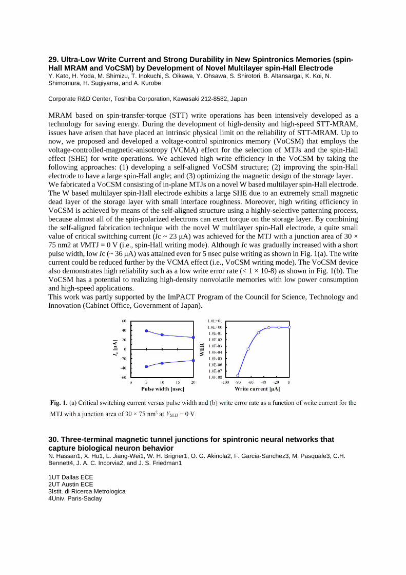
29. Ultra-Low Write Current and Strong Durability in New Spintronics Memories (spin-Hall MRAM and VoCSM) by Development of Novel Multilayer spin-Hall Electrode Y. Kato, H. Yoda, M. Shimizu, T. Inokuchi, S. Oikawa, Y. Ohsawa, S. Shirotori, B. Altansargai, K. Koi, N. Shimomura, H. Sugiyama, and A. Kurobe Corporate R&D Center, Toshiba Corporation, Kawasaki 212-8582, Japan MRAM based on spin-transfer-torque (STT) write operations has been intensively developed as a technology for saving energy. During the development of high-density and high-speed STT-MRAM, issues have arisen that have placed an intrinsic physical limit on the reliability of STT-MRAM. Up to now, we proposed and developed a voltage-control spintronics memory (VoCSM) that employs the voltage-controlled-magnetic-anisotropy (VCMA) effect for the selection of MTJs and the spin-Hall effect (SHE) for write operations. We achieved high write efficiency in the VoCSM by taking the following approaches: (1) developing a self-aligned VoCSM structure; (2) improving the spin-Hall electrode to have a large spin-Hall angle; and (3) optimizing the magnetic design of the storage layer. We fabricated a VoCSM consisting of in-plane MTJs on a novel W based multilayer spin-Hall electrode. The W based multilayer spin-Hall electrode exhibits a large SHE due to an extremely small magnetic dead layer of the storage layer with small interface roughness. Moreover, high writing efficiency in VoCSM is achieved by means of the self-aligned structure using a highly-selective patterning process, because almost all of the spin-polarized electrons can exert torque on the storage layer. By combining the self-aligned fabrication technique with the novel W multilayer spin-Hall electrode, a quite small value of critical switching current (Ic ~ 23 µA) was achieved for the MTJ with a junction area of 30 × 75 nm2 at VMTJ = 0 V (i.e., spin-Hall writing mode). Although Ic was gradually increased with a short pulse width, low Ic (~ 36 µA) was attained even for 5 nsec pulse writing as shown in Fig. 1(a). The write current could be reduced further by the VCMA effect (i.e., VoCSM writing mode). The VoCSM device also demonstrates high reliability such as a low write error rate (< 1 × 10⁻⁸) as shown in Fig. 1(b). The VoCSM has a potential to realizing high-density nonvolatile memories with low power consumption and high-speed applications. This work was partly supported by the ImPACT Program of the Council for Science, Technology and Innovation (Cabinet Office, Government of Japan).
30. Three-terminal magnetic tunnel junctions for spintronic neural networks that capture biological neuron behavior N. Hassan1, X. Hu1, L. Jiang-Wei1, W. H. Brigner1, O. G. Akinola2, F. Garcia-Sanchez3, M. Pasquale3, C.H. Bennett4, J. A. C. Incorvia2, and J. S. Friedman1 1UT Dallas ECE 2UT Austin ECE 3Istit. di Ricerca Metrologica 4Univ. Paris-Saclay

Neuromorphic computing takes inspiration from the way the biological brain operates, with a colocalized memory and logic system where memory is distributed with the processing. It is extremely efficient at tasks that require massive amounts of data to be processed (e.g., recognition, classification, and prediction). To implement neuromorphic computers, a significant challenge exists in creating high-density neural networks with all the necessary biological functions represented. Leaky, integrate, and fire (LIF) neurons need to capture the behavior of integration, firing, leaking back to their original state, and lateral inhibition: if one neuron wins out, it inhibits the firing of nearby neurons1. MRAM-based devices are particularly suitable to act as such neuromorphic computing elements, because they have high endurance for data-intensive tasks and have complex behaviors that can be mapped onto the neuromorphic system. We will present modeling results showing three-terminal magnetic tunnel junctions (3T-MTJs) with mobile domain walls (DWs)2 can perform all the above neuron functions, without the need for external circuitry. A cartoon of two neurons is shown in Fig. 1a. The neuron has a ferromagnetic track with a domain wall and a MTJ on top. Input currents applied to the neurons enable integration by pushing the DWs through spin-transfer or spin-orbit torque. Leaking is performed by a ferromagnet under the 3T-MTJ that creates a magnetic field to constantly push the DWs in the direction opposite of integration. Firing occurs when the DW crosses below the MTJ. Analog lateral inhibition is achieved by dipolar fields from each neuron that attempt to orient neighboring neurons antiparallel by repulsive coupling. Applying this lateral inhibition to a ten-neuron output layer within a neuromorphic crossbar structure, we show in simulation the identification of handwritten digits with a 94% success rate 3.
References 1. N. Burkitt. Biol. Cybern. 95, 1–19 (2006). 2. J. A. Currivan-Incorvia, S. Siddiqui, S. Dutta, et. al. 2015 IEEE Int. Electron Devices Meet. 32–36 (2015). 3. N. Hassan, X. Hu, L. Jiang-Wei, et al. J. Appl. Phys. Accepted. 31. Bit Error Tolerance in MRAM-Based Binarized Neural Networks T. Hirtzlin1, M. Bocquet2, N. Locatelli1, A. F. Vincent1, J.-O Klein1, J.-M Portal2 and D. Querlioz1 1C2N, CNRS, Univ Paris-Sud, Université Paris-Saclay, 91405 Orsay, France Email: [email protected], [email protected] 2Aix Marseille Univ, Université de Toulon, CNRS, IM2NP, Marseille, France One of the most exciting applications of Spin Torque Magnetoresistive Random Access Memory (ST-MRAM) is the in-memory implementation of deep neural networks, which could allow improving the energy efficiency of Artificial Intelligence by orders of magnitude with regards to its implementation on computers and graphics cards. A particularly stimulating vision is using ST-MRAM for implementing Binarized Neural Networks (BNNs), a class of deep neural networks discovered in 2016, which can achieve state-of-the-art performance with a highly reduced memory footprint with regards to
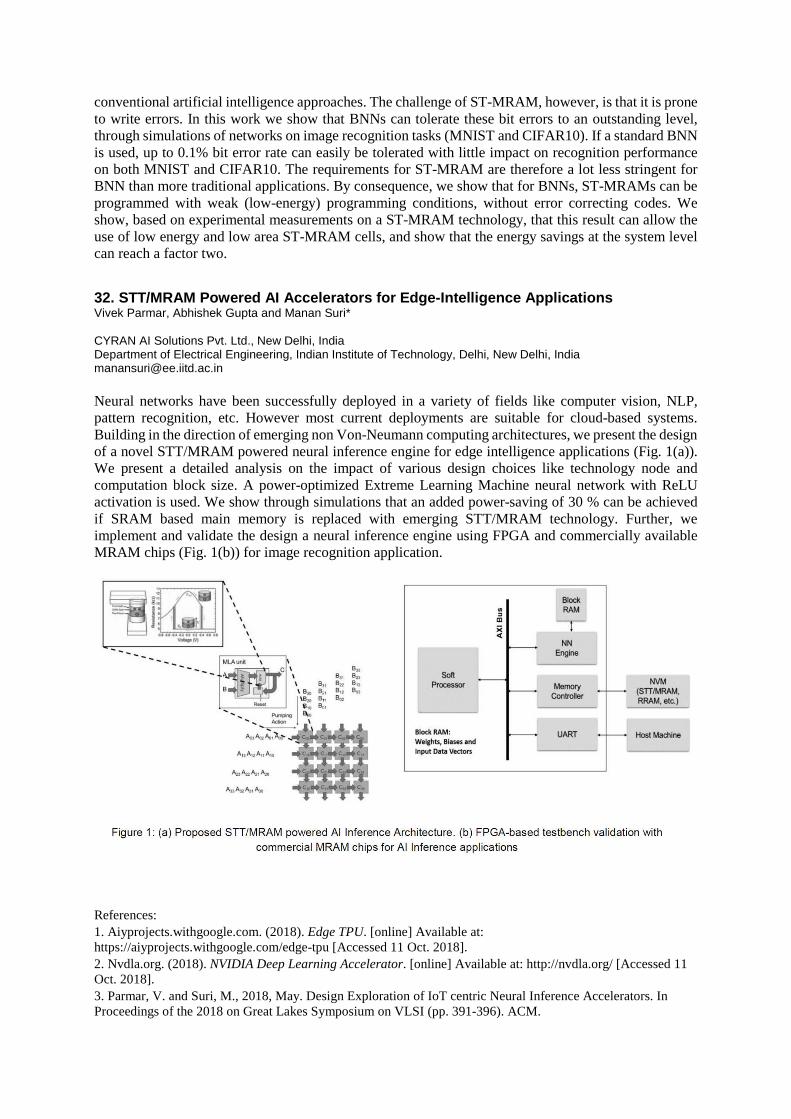
conventional artificial intelligence approaches. The challenge of ST-MRAM, however, is that it is prone to write errors. In this work we show that BNNs can tolerate these bit errors to an outstanding level, through simulations of networks on image recognition tasks (MNIST and CIFAR10). If a standard BNN is used, up to 0.1% bit error rate can easily be tolerated with little impact on recognition performance on both MNIST and CIFAR10. The requirements for ST-MRAM are therefore a lot less stringent for BNN than more traditional applications. By consequence, we show that for BNNs, ST-MRAMs can be programmed with weak (low-energy) programming conditions, without error correcting codes. We show, based on experimental measurements on a ST-MRAM technology, that this result can allow the use of low energy and low area ST-MRAM cells, and show that the energy savings at the system level can reach a factor two. 32. STT/MRAM Powered AI Accelerators for Edge-Intelligence Applications Vivek Parmar, Abhishek Gupta and Manan Suri* CYRAN AI Solutions Pvt. Ltd., New Delhi, India Department of Electrical Engineering, Indian Institute of Technology, Delhi, New Delhi, India [email protected] Neural networks have been successfully deployed in a variety of fields like computer vision, NLP, pattern recognition, etc. However most current deployments are suitable for cloud-based systems. Building in the direction of emerging non Von-Neumann computing architectures, we present the design of a novel STT/MRAM powered neural inference engine for edge intelligence applications (Fig. 1(a)). We present a detailed analysis on the impact of various design choices like technology node and computation block size. A power-optimized Extreme Learning Machine neural network with ReLU activation is used. We show through simulations that an added power-saving of 30 % can be achieved if SRAM based main memory is replaced with emerging STT/MRAM technology. Further, we implement and validate the design a neural inference engine using FPGA and commercially available MRAM chips (Fig. 1(b)) for image recognition application.
References: 1. Aiyprojects.withgoogle.com. (2018). Edge TPU. [online] Available at: https://aiyprojects.withgoogle.com/edge-tpu [Accessed 11 Oct. 2018]. 2. Nvdla.org. (2018). NVIDIA Deep Learning Accelerator. [online] Available at: http://nvdla.org/ [Accessed 11 Oct. 2018]. 3. Parmar, V. and Suri, M., 2018, May. Design Exploration of IoT centric Neural Inference Accelerators. In Proceedings of the 2018 on Great Lakes Symposium on VLSI (pp. 391-396). ACM.


![Enhancement Mode Strained (1.3%) Germanium Quantum Well ... · [1] IEDM, 2010 [1] IEDM, 2010 [3] IEDM, 2005 w/ GeOx IL Hole Mobility [cm 2 /Vs] EOT [A] [2] VLSI, 2009 This work w](https://img.pdfslide.net/doc/110x75/5e3951d9b374ef06753694cd/enhancement-mode-strained-13-germanium-quantum-well-1-iedm-2010-1-iedm.jpg)