Embed Size (px)
Citation preview
Product Specification
LM215WF3Liquid Crystal Display
Ver. 1.0 Nov., 15, 2012 1 / 35
SPECIFICATIONFOR
APPROVAL
21.5” Full HD TFT LCDTitle
MODEL
BUYER SUPPLIER LG Display Co., Ltd.
*MODEL LM215WF3
SUFFIX SLK1
NECP
*When you obtain standard approval,please use the above model name without suffix
APPROVED BY SIGNATURE DATE
/
/
/
Please return 1 copy for your confirmation with
your signature and comments.
APPROVED BY SIGNATURE DATE
C.K. Lee / G. Manager
REVIEWED BY
J.H. Song / Manager [C]
H.D. Joo / Manager [M]
C.S. Shin / Manager [P]
PREPARED BY
K.W. Lee / Engineer
MNT Products Engineering Dept.LG Display Co., Ltd
( ) Preliminary Specification( ● ) Final Specification
Product Specification
LM215WF3Liquid Crystal Display
Ver. 1.0 Nov., 15, 2012 2 / 35
Contents
32PACKING FORM8-2
No ITEM Page
COVER 1
CONTENTS 2
RECORD OF REVISIONS 3
1 GENERAL DESCRIPTION 4
2 ABSOLUTE MAXIMUM RATINGS 5
3 ELECTRICAL SPECIFICATIONS 6
3-1 ELECTRICAL CHARACTREISTICS 6
3-2 INTERFACE CONNECTIONS 9
3-3 SIGNAL TIMING SPECIFICATIONS 14
3-4 SIGNAL TIMING WAVEFORMS 15
3-5 COLOR INPUT DATA REFERNECE 16
3-6 POWER SEQUENCE 17
3-7 VLCD Power Dip Condition 18
4 OPTICAL SPECIFICATIONS 19
5 MECHANICAL CHARACTERISTICS 25
6 RELIABLITY 28
7 INTERNATIONAL STANDARDS 29
7-1 SAFETY 29
7-2 EMC 29
7-3 ENVIRONMENT 29
8 PACKING 30
8-1 DESIGNATION OF LOT MARK 30
8-3 PALLET FORM 33
9 PRECAUTIONS 34
Product Specification
LM215WF3Liquid Crystal Display
Ver. 1.0 Nov., 15, 2012 3 / 35
RECORD OF REVISIONS
Revision No
Revision Date Page Description
0.0 Sep., 06, 2012 - First Draft, Preliminary Specifications
0.1 Sep., 19, 2012 9 Add Note 4. ITLC Input voltage spec.
17 Add power sequence about option signal (ITLC)
29 Update the rear drawing
30 Change package quantity in one box (12pcb → 14pcb)
0.2 Oct., 26, 2012 6 Add the value of LVDS impedance
8 Update the LED Max. power consumption
11 Add “Maximum deviation of input clock freq during SSC”
Add “Maximum modulation freq of input clock during SSC”
19 Update the Color Coordinates
29 Update the rear drawing
30 Add Product Label description
31, 32,33
Add Packing assembly description
0.3 Nov., 14, 2012 19 Add color gamut spec.
1.0 Nov., 15, 2012 - Firth Draft, Final Specifications
Product Specification
LM215WF3Liquid Crystal Display
Ver. 1.0 Nov., 15, 2012 4 / 35
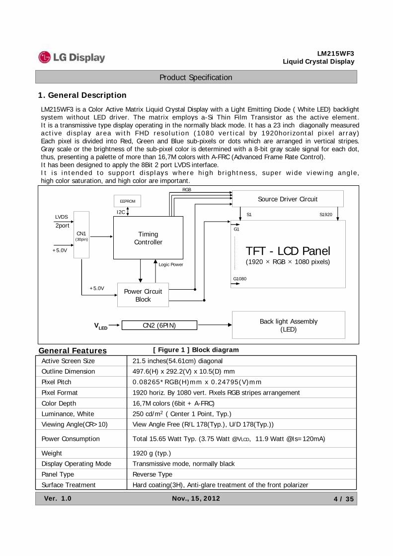
1. General Description
General FeaturesActive Screen Size 21.5 inches(54.61cm) diagonal
Outline Dimension 497.6(H) x 292.2(V) x 10.5(D) mm
Pixel Pitch 0.08265*RGB(H)mm x 0.24795(V)mm
Pixel Format 1920 horiz. By 1080 vert. Pixels RGB stripes arrangement
Color Depth 16,7M colors (6bit + A-FRC)
Luminance, White 250 cd/m2 ( Center 1 Point, Typ.)
Viewing Angle(CR>10) View Angle Free (R/L 178(Typ.), U/D 178(Typ.))
Power Consumption Total 15.65 Watt Typ. (3.75 Watt @VLCD, 11.9 Watt @Is=120mA)
Weight 1920 g (typ.)
Display Operating Mode Transmissive mode, normally black
Panel Type Reverse Type
Surface Treatment Hard coating(3H), Anti-glare treatment of the front polarizer
LM215WF3 is a Color Active Matrix Liquid Crystal Display with a Light Emitting Diode ( White LED) backlight system without LED driver. The matrix employs a-Si Thin Film Transistor as the active element.It is a transmissive type display operating in the normally black mode. It has a 23 inch diagonally measured act i ve display a rea wi th FHD resolut ion (1080 ver t i cal by 1920horizontal pixel array)Each pixel is divided into Red, Green and Blue sub-pixels or dots which are arranged in vertical stripes.Gray scale or the brightness of the sub-pixel color is determined with a 8-bit gray scale signal for each dot,thus, presenting a palette of more than 16,7M colors with A-FRC (Advanced Frame Rate Control).It has been designed to apply the 8Bit 2 port LVDS interface.I t i s i ntended to support displays where high brightness, super wide viewing angle,high color saturation, and high color are important.
[ Figure 1 ] Block diagram
CN1(30pin)
LVDS
2port
+5.0V
Source Driver Circuit
TFT - LCD Panel(1920 × RGB × 1080 pixels)
S1 S1920
Back light Assembly(LED)
+5.0V
CN2 (6PIN)VLED
EEPROM
I2C
RGB
Logic Power
Power Circuit Block
G1
G1080
TimingController
Product Specification
LM215WF3Liquid Crystal Display
Ver. 1.0 Nov., 15, 2012 5 / 35
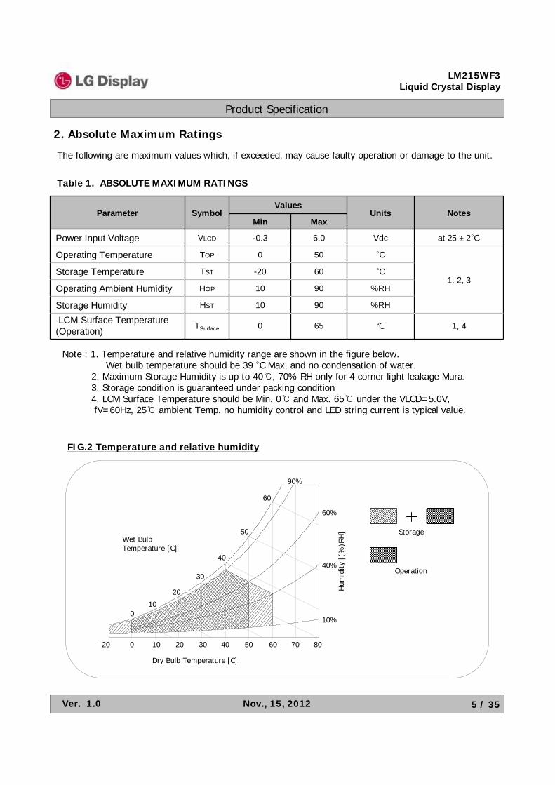
2. Absolute Maximum Ratings
The following are maximum values which, if exceeded, may cause faulty operation or damage to the unit.
Note : 1. Temperature and relative humidity range are shown in the figure below. Wet bulb temperature should be 39 °C Max, and no condensation of water.
2. Maximum Storage Humidity is up to 40℃, 70% RH only for 4 corner light leakage Mura.3. Storage condition is guaranteed under packing condition4. LCM Surface Temperature should be Min. 0℃ and Max. 65℃ under the VLCD=5.0V, fV=60Hz, 25℃ ambient Temp. no humidity control and LED string current is typical value.
Table 1. ABSOLUTE MAXIMUM RATINGS
1, 2, 3
°C500TOPOperating Temperature
°C60-20TSTStorage Temperature
%RH9010HOPOperating Ambient Humidity
%RH9010HSTStorage Humidity
Parameter SymbolValues
Units NotesMin Max
Power Input Voltage VLCD -0.3 6.0 Vdc at 25 ± 2°C
1, 4LCM Surface Temperature(Operation) TSurface 0 65 ℃
90%
10 20 30 40 50 60 70 800-20
010
20
30
40
50
Dry Bulb Temperature [C]
Wet BulbTemperature [C]
Storage
Operation
Hum
idity
[(%
)RH
]
10%
40%
60%
60
FIG.2 Temperature and relative humidity
Product Specification
LM215WF3Liquid Crystal Display
Ver. 1.0 Nov., 15, 2012 6 / 35
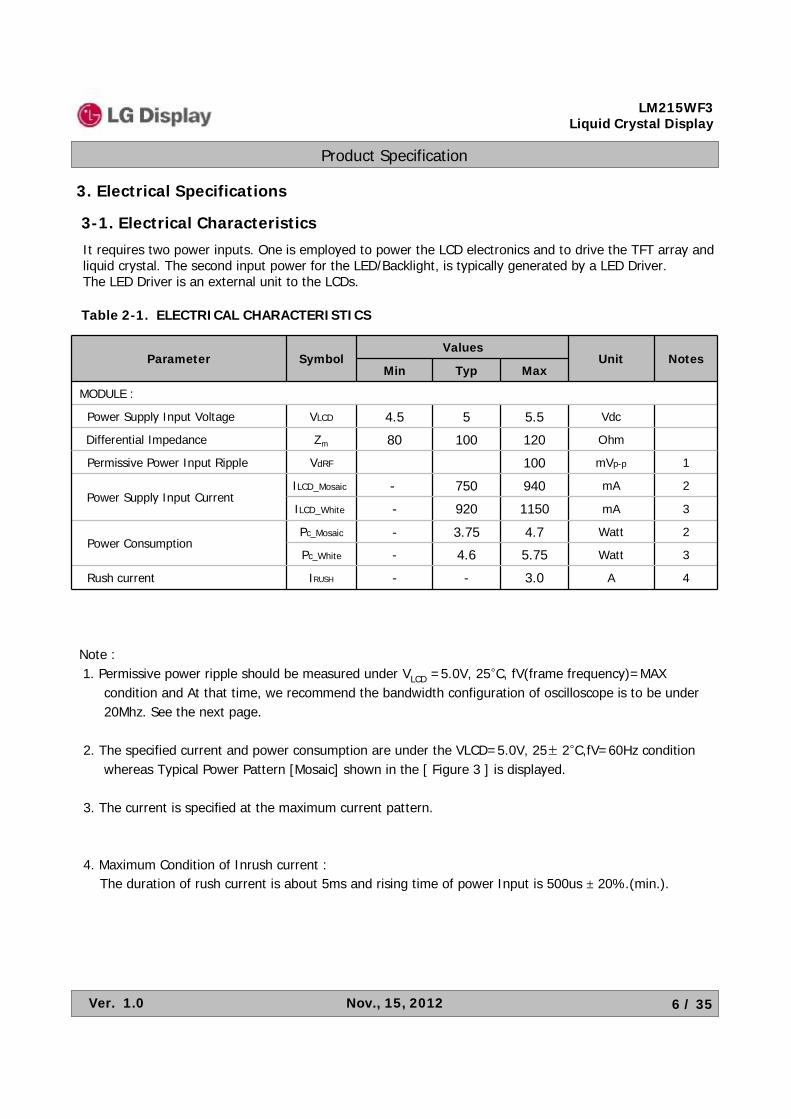
3. Electrical Specifications
3-1. Electrical Characteristics
Table 2-1. ELECTRICAL CHARACTERISTICS
Note : 1. Permissive power ripple should be measured under VLCD =5.0V, 25°C, fV(frame frequency)=MAX
condition and At that time, we recommend the bandwidth configuration of oscilloscope is to be under20Mhz. See the next page.
2. The specified current and power consumption are under the VLCD=5.0V, 25± 2°C,fV=60Hz condition whereas Typical Power Pattern [Mosaic] shown in the [ Figure 3 ] is displayed.
3. The current is specified at the maximum current pattern.
4. Maximum Condition of Inrush current : The duration of rush current is about 5ms and rising time of power Input is 500us ± 20%.(min.).
It requires two power inputs. One is employed to power the LCD electronics and to drive the TFT array and liquid crystal. The second input power for the LED/Backlight, is typically generated by a LED Driver. The LED Driver is an external unit to the LCDs.
Ohm12010080ZmDifferential Impedance
Parameter SymbolValues
Unit NotesMin Typ Max
MODULE :
Power Supply Input Voltage VLCD 4.5 5 5.5 Vdc
Permissive Power Input Ripple VdRF 100 mVp-p 1
Power Supply Input CurrentILCD_Mosaic - 750 940 mA 2
ILCD_White - 920 1150 mA 3
Power ConsumptionPc_Mosaic - 3.75 4.7 Watt 2
Pc_White - 4.6 5.75 Watt 3
Rush current IRUSH - - 3.0 A 4
Product Specification
LM215WF3Liquid Crystal Display
Ver. 1.0 Nov., 15, 2012 7 / 35
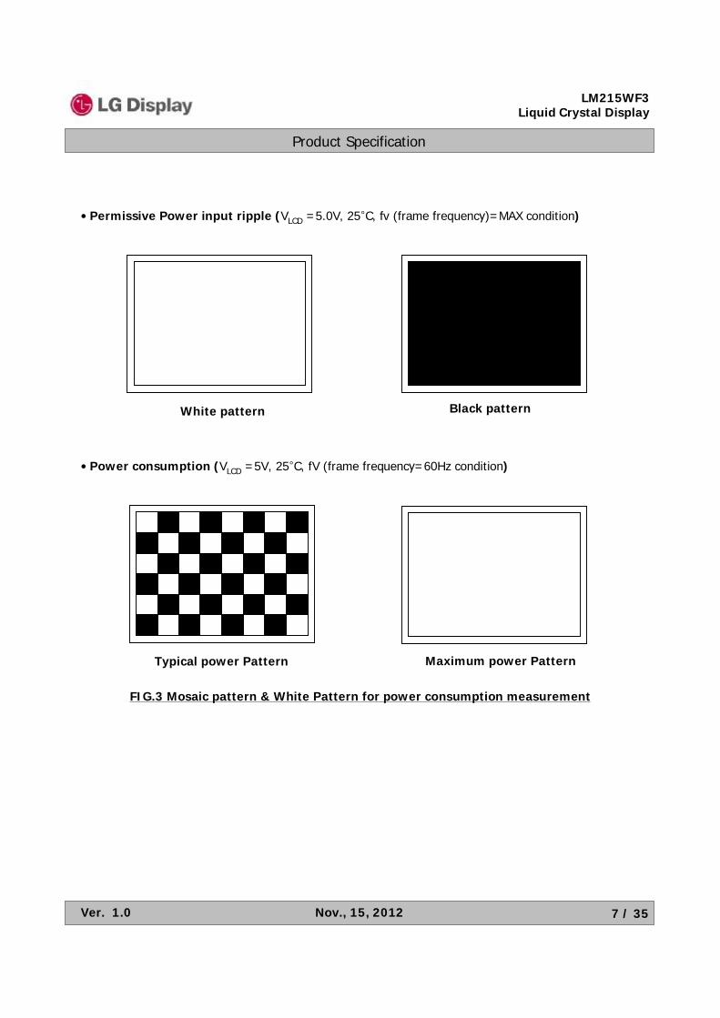
White pattern Black pattern
• Permissive Power input ripple (VLCD =5.0V, 25°C, fv (frame frequency)=MAX condition)
• Power consumption (VLCD =5V, 25°C, fV (frame frequency=60Hz condition)
Typical power Pattern Maximum power Pattern
FIG.3 Mosaic pattern & White Pattern for power consumption measurement
Product Specification
LM215WF3Liquid Crystal Display
Ver. 1.0 Nov., 15, 2012 8 / 35
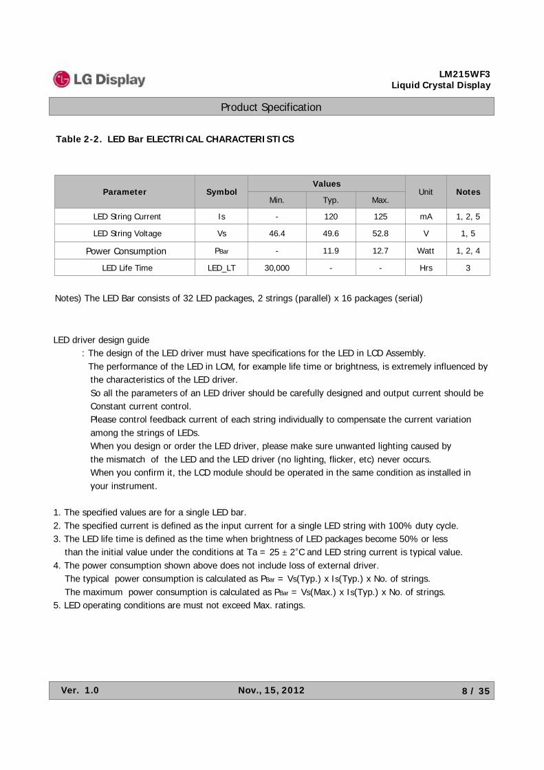
Table 2-2. LED Bar ELECTRICAL CHARACTERISTICS
Parameter SymbolValues
Unit NotesMin. Typ. Max.
LED String Current Is - 120 125 mA 1, 2, 5
LED String Voltage Vs 46.4 49.6 52.8 V 1, 5
Power Consumption PBar - 11.9 12.7 Watt 1, 2, 4
LED Life Time LED_LT 30,000 - - Hrs 3
LED driver design guide: The design of the LED driver must have specifications for the LED in LCD Assembly.
The performance of the LED in LCM, for example life time or brightness, is extremely influenced bythe characteristics of the LED driver. So all the parameters of an LED driver should be carefully designed and output current should be Constant current control.Please control feedback current of each string individually to compensate the current variation among the strings of LEDs.When you design or order the LED driver, please make sure unwanted lighting caused by the mismatch of the LED and the LED driver (no lighting, flicker, etc) never occurs.When you confirm it, the LCD module should be operated in the same condition as installed in your instrument.
1. The specified values are for a single LED bar.2. The specified current is defined as the input current for a single LED string with 100% duty cycle.3. The LED life time is defined as the time when brightness of LED packages become 50% or less
than the initial value under the conditions at Ta = 25 ± 2°C and LED string current is typical value.4. The power consumption shown above does not include loss of external driver.
The typical power consumption is calculated as PBar = Vs(Typ.) x Is(Typ.) x No. of strings. The maximum power consumption is calculated as PBar = Vs(Max.) x Is(Typ.) x No. of strings.
5. LED operating conditions are must not exceed Max. ratings.
Notes) The LED Bar consists of 32 LED packages, 2 strings (parallel) x 16 packages (serial)
Product Specification
LM215WF3Liquid Crystal Display
Ver. 1.0 Nov., 15, 2012 9 / 35
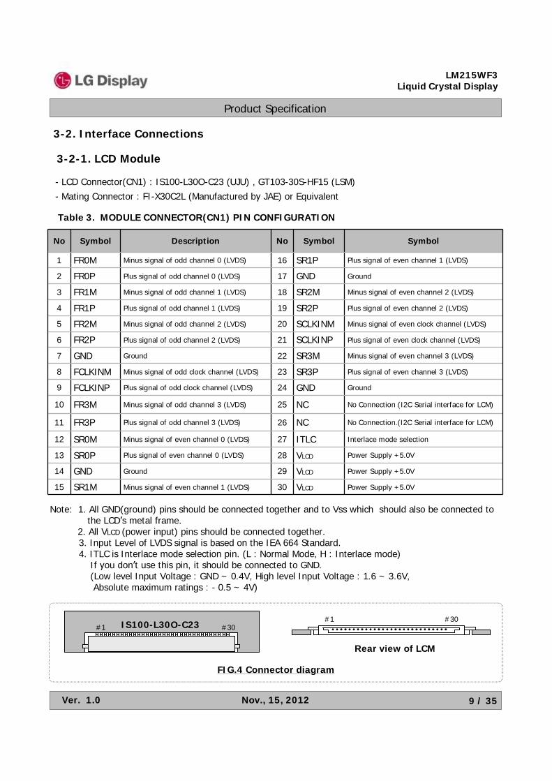
3-2. Interface Connections
Table 3. MODULE CONNECTOR(CN1) PIN CONFIGURATION
3-2-1. LCD Module
Note: 1. All GND(ground) pins should be connected together and to Vss which should also be connected to the LCD’s metal frame.
2. All VLCD (power input) pins should be connected together.3. Input Level of LVDS signal is based on the IEA 664 Standard.4. ITLC is Interlace mode selection pin. (L : Normal Mode, H : Interlace mode)
If you don’t use this pin, it should be connected to GND.(Low level Input Voltage : GND ~ 0.4V, High level Input Voltage : 1.6 ~ 3.6V, Absolute maximum ratings : - 0.5 ~ 4V)
#1 #30#1
Rear view of LCM
#30
No Symbol Description No Symbol Symbol
1 FR0M Minus signal of odd channel 0 (LVDS) 16 SR1P Plus signal of even channel 1 (LVDS)
2 FR0P Plus signal of odd channel 0 (LVDS) 17 GND Ground
3 FR1M Minus signal of odd channel 1 (LVDS) 18 SR2M Minus signal of even channel 2 (LVDS)
4 FR1P Plus signal of odd channel 1 (LVDS) 19 SR2P Plus signal of even channel 2 (LVDS)
5 FR2M Minus signal of odd channel 2 (LVDS) 20 SCLKINM Minus signal of even clock channel (LVDS)
6 FR2P Plus signal of odd channel 2 (LVDS) 21 SCLKINP Plus signal of even clock channel (LVDS)
7 GND Ground 22 SR3M Minus signal of even channel 3 (LVDS)
8 FCLKINM Minus signal of odd clock channel (LVDS) 23 SR3P Plus signal of even channel 3 (LVDS)
9 FCLKINP Plus signal of odd clock channel (LVDS) 24 GND Ground
10 FR3M Minus signal of odd channel 3 (LVDS) 25 NC No Connection (I2C Serial interface for LCM)
11 FR3P Plus signal of odd channel 3 (LVDS) 26 NC No Connection.(I2C Serial interface for LCM)
12 SR0M Minus signal of even channel 0 (LVDS) 27 ITLC Interlace mode selection
13 SR0P Plus signal of even channel 0 (LVDS) 28 VLCD Power Supply +5.0V
14 GND Ground 29 VLCD Power Supply +5.0V
15 SR1M Minus signal of even channel 1 (LVDS) 30 VLCD Power Supply +5.0V
- LCD Connector(CN1) : IS100-L30O-C23 (UJU) , GT103-30S-HF15 (LSM)- Mating Connector : FI-X30C2L (Manufactured by JAE) or Equivalent
IS100-L30O-C23
FIG.4 Connector diagram
Product Specification
LM215WF3Liquid Crystal Display
Ver. 1.0 Nov., 15, 2012 10 / 35
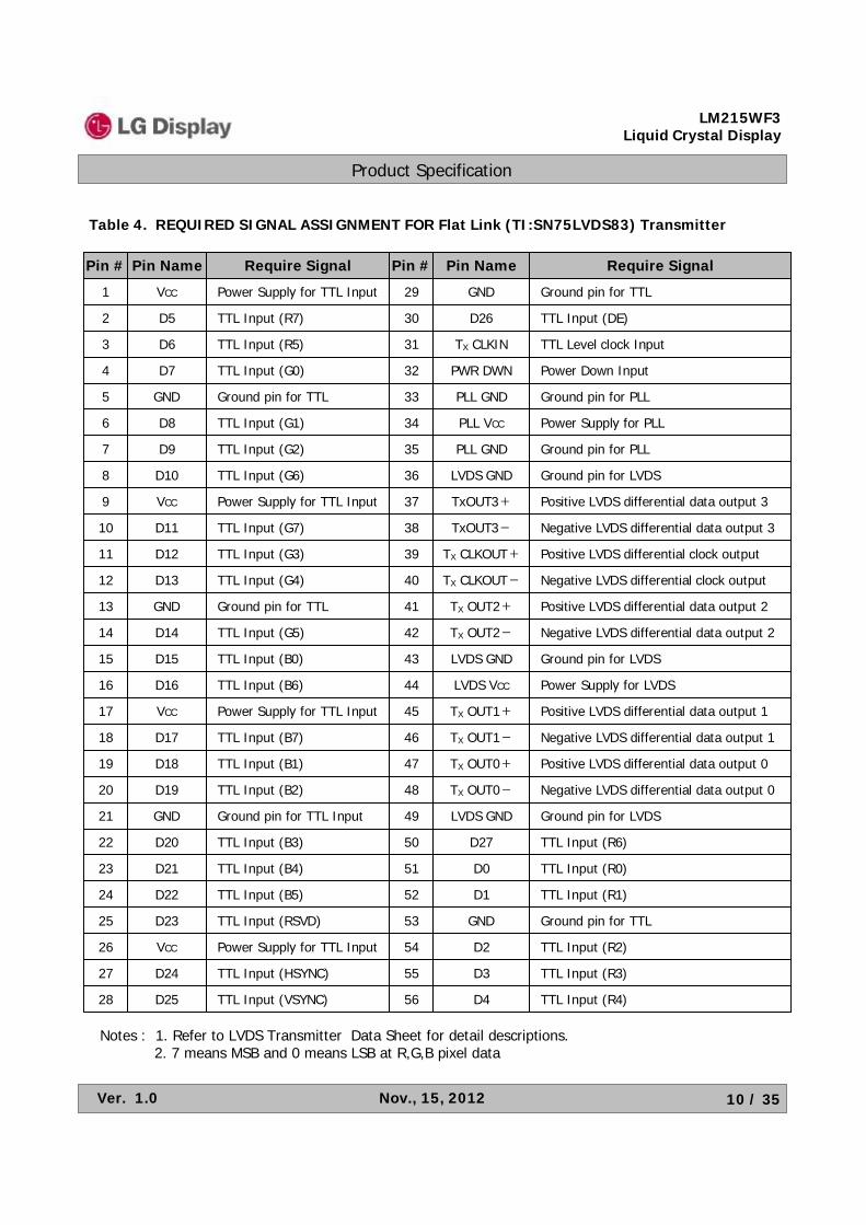
Table 4. REQUIRED SIGNAL ASSIGNMENT FOR Flat Link (TI:SN75LVDS83) Transmitter
Pin # Require SignalPin Name Pin # Require SignalPin Name
1 Power Supply for TTL InputVCC 29 Ground pin for TTLGND
2 TTL Input (R7)D5 30 TTL Input (DE)D26
3 TTL Input (R5)D6 31 TTL Level clock InputTX CLKIN
4 TTL Input (G0)D7 32 Power Down InputPWR DWN
5 Ground pin for TTLGND 33 Ground pin for PLLPLL GND
6 TTL Input (G1)D8 34 Power Supply for PLLPLL VCC
7 TTL Input (G2)D9 35 Ground pin for PLLPLL GND
8 TTL Input (G6)D10 36 Ground pin for LVDSLVDS GND
9 Power Supply for TTL InputVCC 37 Positive LVDS differential data output 3TxOUT3+
10 TTL Input (G7)D11 38 Negative LVDS differential data output 3TxOUT3-
11 TTL Input (G3)D12 39 Positive LVDS differential clock outputTX CLKOUT+
12 TTL Input (G4)D13 40 Negative LVDS differential clock outputTX CLKOUT-
13 Ground pin for TTLGND 41 Positive LVDS differential data output 2TX OUT2+
14 TTL Input (G5)D14 42 Negative LVDS differential data output 2TX OUT2-
15 TTL Input (B0)D15 43 Ground pin for LVDSLVDS GND
16 TTL Input (B6)D16 44 Power Supply for LVDSLVDS VCC
17 Power Supply for TTL InputVCC 45 Positive LVDS differential data output 1TX OUT1+
46 Negative LVDS differential data output 1TX OUT1-18 TTL Input (B7)D17
47 Positive LVDS differential data output 0TX OUT0+
48 Negative LVDS differential data output 0TX OUT0-
19 TTL Input (B1)D18
20 TTL Input (B2)D19
49 Ground pin for LVDSLVDS GND21 Ground pin for TTL InputGND
22 TTL Input (B3)D20
23 TTL Input (B4)D21
50 TTL Input (R6)D27
51 TTL Input (R0)D0
24 TTL Input (B5)D22
25 TTL Input (RSVD)D23
52 TTL Input (R1)D1
53 Ground pin for TTLGND
26 Power Supply for TTL InputVCC 54 TTL Input (R2)D2
55 TTL Input (R3)D327 TTL Input (HSYNC)D24
56 TTL Input (R4)D428 TTL Input (VSYNC)D25
Notes : 1. Refer to LVDS Transmitter Data Sheet for detail descriptions.2. 7 means MSB and 0 means LSB at R,G,B pixel data
Product Specification
LM215WF3Liquid Crystal Display
Ver. 1.0 Nov., 15, 2012 11 / 35
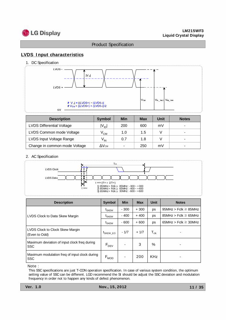
LVDS Input characteristics
-%3-FDEVMaximum deviation of input clock freq during SSC
-KHz200-FMODMaximum modulation freq of input clock during SSC
-Tclk+ 1/7- 1/7tSKEW_EOLVDS Clock to Clock Skew Margin (Even to Odd)
Description Symbol Min Max Unit Notes
LVDS Clock to Data Skew Margin
tSKEW - 300 + 300 ps 95MHz > Fclk ≥ 85MHz
tSKEW - 400 + 400 ps 85MHz > Fclk ≥ 65MHz
tSKEW - 600 + 600 ps 65MHz > Fclk ≥ 30MHz
1. DC Specification
2. AC Specification
LVDS Data
t SKEW
LVDS Clock
Tclk
t SKEW (Fclk = 1/Tclk)1) 95MHz > Fclk ≥ 85MHz : -300 ~ +3002) 85MHz > Fclk ≥ 65MHz : -400 ~ +4003) 65MHz > Fclk ≥ 30MHz : -600 ~ +600
-V1.80.7VINLVDS Input Voltage Range
-mV250-ΔVCMChange in common mode Voltage
-V1.51.0VCMLVDS Common mode Voltage
-mV600200|VID|LVDS Differential Voltage
NotesUnitMaxMinSymbolDescription
Note : This SSC specifications are just T-CON operation specification. In case of various system condition, the optimumsetting value of SSC can be different. LGD recommend the SI should be adjust the SSC deviation and modulationfrequency in order not to happen any kinds of defect phenomenon.
Product Specification
LM215WF3Liquid Crystal Display
Ver. 1.0 Nov., 15, 2012 12 / 35
< Clock skew margin between channel >
< LVDS Data Format >
3. Data Format1) LVDS 2 Port
Product Specification
LM215WF3Liquid Crystal Display
Ver. 1.0 Nov., 15, 2012 13 / 35
Table 5. BACKLIGHT CONNECTOR PIN CONFIGURATION(CN2)
The LED interface connector is a model SM06B-SHJH(HF), wire-locking type manufactured by JST.The mating connector is a SHJP-06V-S(HF) or SHJP-06V-A-K(HF) and Equivalent.The pin configuration for the connector is shown in the table below.
Pin Symbol Description Notes
1 FB1 Channel1 Current Feedback
2 NC No Connection
3 VLED LED Power Supply
4 VLED LED Power Supply
5 NC No Connection
6 FB2 Channel2 Current Feedback
[ Figure 5 ] Backlight connector view
Rear view of LCM
#1
#6
Product Specification
LM215WF3Liquid Crystal Display
Ver. 1.0 Nov., 15, 2012 14 / 35
3-3. Signal Timing SpecificationsThis is signal timing required at the input of the TMDS transmitter. All of the interface signal timing should besatisfied with the following specifications for it’s proper operation.
Table 6. TIMING TABLE
Note: Hsync period and Hsync width-active should be even number times of tCLK. If the value is odd number times of tCLK, display control signal can be asynchronous. In order to operate this LCM a Hsync, Vsyn, and DE(data enable) signals should be used.
1. The performance of the electro-optical characteristics may be influenced by variance of the verticalrefresh rates.
2. Vsync and Hsync should be keep the above specification.3. Hsync Period, Hsync Width, and Horizontal Back Porch should be any times of of character
number(4).4. The polarity of Hsync, Vsync is not restricted.5. The Max frequency of 1920X1080 resolution is 82.5Mhz
ITEM Symbol Min Typ Max Unit Note
DCLKPeriod tCLK 11.43 13.89 16.7 ns
Frequency - 60 72 87.5 MHz 5
Hsync
Period tHP 1024 1088 1120 tCLK
Horizontal Valid tHV 960 960 960 tCLK
Horizontal Blank tHB 64 128 160
Frequency fH 64 66 83 KHz
Width tWH 16 32 48 tCLK
Horizontal Back Porch tHBP 32 48 64
Horizontal Front Porch tHFP 16 48 48
Vsync
Period tVP 1090 1100 1160 tHP
Vertical Valid tVV 1080 1080 1080 tHP
Vertical Blank tVB 10 20 80 tHP
Frequency fV 50 60 75 Hz
Width tWV 2 4 16 tHP
Vertical Back Porch tVBP 5 8 32
Vertical Front Porch tVFP 3 8 32
Product Specification
LM215WF3Liquid Crystal Display
Ver. 1.0 Nov., 15, 2012 15 / 35
3-4. Signal Timing Waveforms
DE(Data Enable)
tVV
tVP
DE
DE(Data Enable)
tHP
tHV
DE
1. DCLK , DE, DATA waveforms
2. Horizontal waveform
3. Vertical waveform
tHP
tCLK
Invalid data
Valid data
Invalid data
Invalid data
Invalid data
Pixel 0,0 Pixel 2,0
Pixel 1,0 Pixel 3,0
DE(Data Enable)
Valid data
DCLK
First data
Second data
Product Specification
LM215WF3Liquid Crystal Display
Ver. 1.0 Nov., 15, 2012 16 / 35
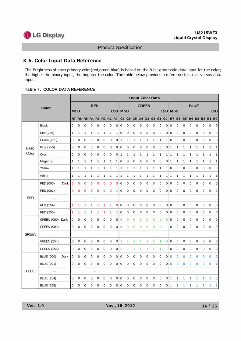
3-5. Color Input Data Reference
Table 7. COLOR DATA REFERENCE
The Brightness of each primary color(red,green,blue) is based on the 8-bit gray scale data input for the color;the higher the binary input, the brighter the color. The table below provides a reference for color versus data input.
Color
Input Color Data
REDMSB LSB
GREENMSB LSB
BLUEMSB LSB
R7 R6 R5 R4 R3 R2 R1 R0 G7 G6 G5 G4 G3 G2 G1 G0 B7 B6 B5 B4 B3 B2 B1 B0
BasicColor
Black 0 0 0 0 0 0 0 0 0 0 0 0 0 0 0 0 0 0 0 0 0 0 0 0
Red (255) 1 1 1 1 1 1 1 1 0 0 0 0 0 0 0 0 0 0 0 0 0 0 0 0
Green (255) 0 0 0 0 0 0 0 0 1 1 1 1 1 1 1 1 0 0 0 0 0 0 0 0
Blue (255) 0 0 0 0 0 0 0 0 0 0 0 0 0 0 0 0 1 1 1 1 1 1 1 1
Cyan 0 0 0 0 0 0 0 0 1 1 1 1 1 1 1 1 1 1 1 1 1 1 1 1
Magenta 1 1 1 1 1 1 1 1 0 0 0 0 0 0 0 0 1 1 1 1 1 1 1 1
Yellow 1 1 1 1 1 1 1 1 1 1 1 1 1 1 1 1 0 0 0 0 0 0 0 0
White 1 1 1 1 1 1 1 1 1 1 1 1 1 1 1 1 1 1 1 1 1 1 1 1
RED
RED (000) Dark 0 0 0 0 0 0 0 0 0 0 0 0 0 0 0 0 0 0 0 0 0 0 0 0
RED (001) 0 0 0 0 0 0 0 1 0 0 0 0 0 0 0 0 0 0 0 0 0 0 0 0
... ... ... ...
RED (254) 1 1 1 1 1 1 1 0 0 0 0 0 0 0 0 0 0 0 0 0 0 0 0 0
RED (255) 1 1 1 1 1 1 1 1 0 0 0 0 0 0 0 0 0 0 0 0 0 0 0 0
GREEN
GREEN (000) Dark 0 0 0 0 0 0 0 0 0 0 0 0 0 0 0 0 0 0 0 0 0 0 0 0
GREEN (001) 0 0 0 0 0 0 0 0 0 0 0 0 0 0 0 1 0 0 0 0 0 0 0 0
... ... ... ...
GREEN (254) 0 0 0 0 0 0 0 0 1 1 1 1 1 1 1 0 0 0 0 0 0 0 0 0
GREEN (255) 0 0 0 0 0 0 0 0 1 1 1 1 1 1 1 1 0 0 0 0 0 0 0 0
BLUE
BLUE (000) Dark 0 0 0 0 0 0 0 0 0 0 0 0 0 0 0 0 0 0 0 0 0 0 0 0
BLUE (001) 0 0 0 0 0 0 0 0 0 0 0 0 0 0 0 0 0 0 0 0 0 0 0 1
... ... ... ...
BLUE (254) 0 0 0 0 0 0 0 0 0 0 0 0 0 0 0 0 1 1 1 1 1 1 1 0
BLUE (255) 0 0 0 0 0 0 0 0 0 0 0 0 0 0 0 0 1 1 1 1 1 1 1 1
Product Specification
LM215WF3Liquid Crystal Display
Ver. 1.0 Nov., 15, 2012 17 / 35
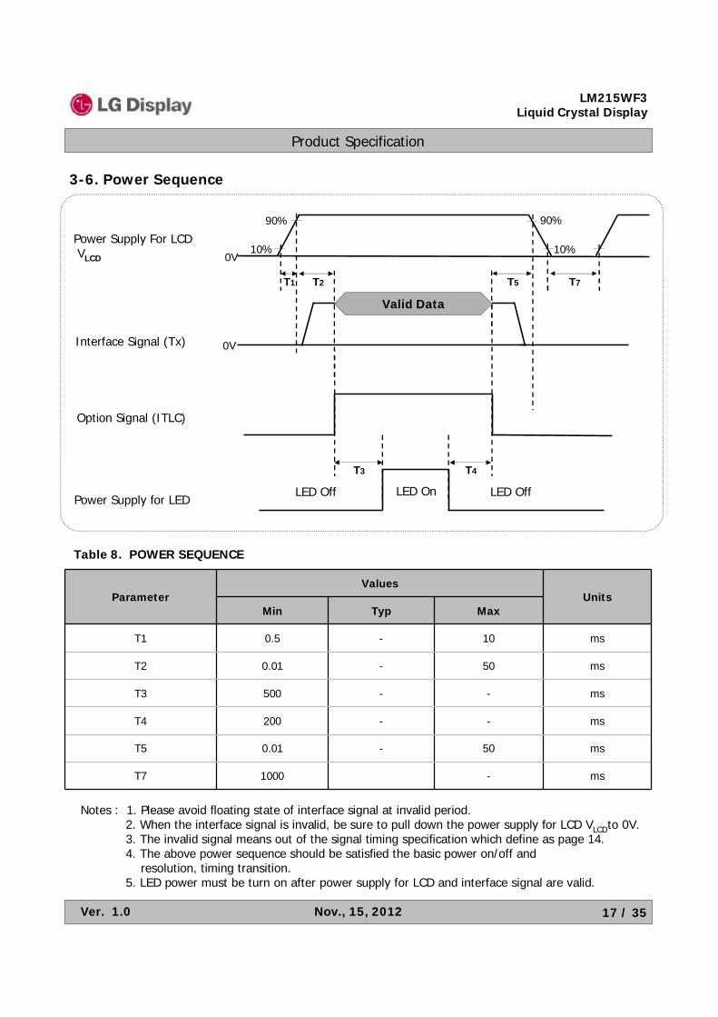
3-6. Power Sequence
Notes : 1. Please avoid floating state of interface signal at invalid period.2. When the interface signal is invalid, be sure to pull down the power supply for LCD VLCDto 0V.3. The invalid signal means out of the signal timing specification which define as page 14.4. The above power sequence should be satisfied the basic power on/off and
resolution, timing transition.5. LED power must be turn on after power supply for LCD and interface signal are valid.
ParameterValues
UnitsMin Typ Max
T1 0.5 - 10 ms
T2 0.01 - 50 ms
T3 500 - - ms
T4 200 - - ms
T5 0.01 - 50 ms
T7 1000 - ms
Table 8. POWER SEQUENCE
Interface Signal (Tx)
Power Supply for LED
Power Supply For LCDVLCD
10%0V
90%
10%
T1 T2 T5 T7
LED On
T3 T4
90%
0V
Valid Data
LED Off LED Off
Option Signal (ITLC)
Product Specification
LM215WF3Liquid Crystal Display
Ver. 1.0 Nov., 15, 2012 18 / 35
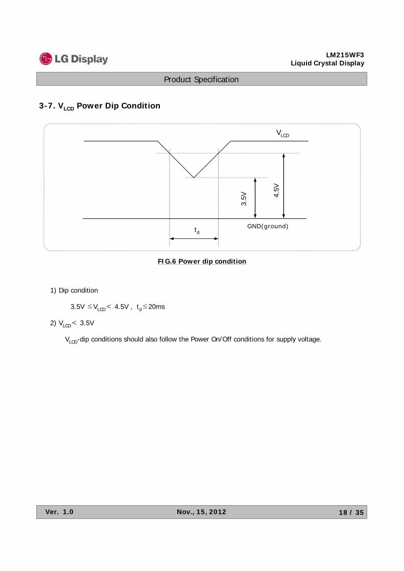
3-7. VLCD Power Dip Condition
1) Dip condition
3.5V ≤VLCD< 4.5V , td≤20ms
2) VLCD< 3.5V
VLCD-dip conditions should also follow the Power On/Off conditions for supply voltage.
4.5V
3.5V
VLCD
td
FIG.6 Power dip condition
GND(ground)
Product Specification
LM215WF3Liquid Crystal Display
Ver. 1.0 Nov., 15, 2012 19 / 35
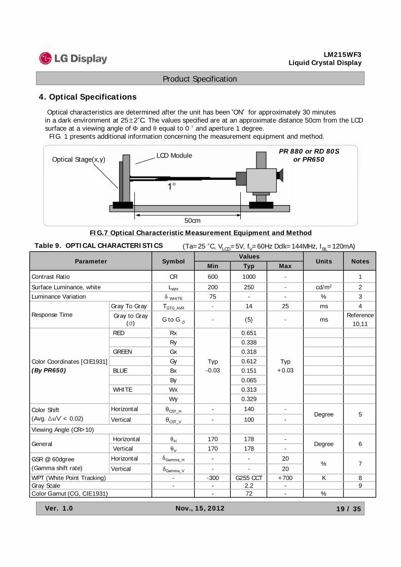
Optical characteristics are determined after the unit has been ‘ON’ for approximately 30 minutesin a dark environment at 25±2°C. The values specified are at an approximate distance 50cm from the LCDsurface at a viewing angle of Φ and θ equal to 0 ° and aperture 1 degree.FIG. 1 presents additional information concerning the measurement equipment and method.
4. Optical Specifications
50cm
Optical Stage(x,y) LCD Module PR 880 or RD 80S or PR650
Table 9. OPTICAL CHARACTERISTICS
FIG.7 Optical Characteristic Measurement Equipment and Method
(Ta=25 °C, VLCD=5V, fV=60Hz Dclk=144MHz, IBL=120mA)
9-2.2--Gray Scale
Parameter SymbolValues
Units NotesMin Typ Max
Contrast Ratio CR 600 1000 - 1
Surface Luminance, white LWH 200 250 - cd/m2 2Luminance Variation δ WHITE 75 - - % 3
Response TimeGray To Gray TGTG_AVR - 14 25 ms 4
Gray to Gray (σ) G to G σ - (5) - ms
Reference10,11
Color Coordinates [CIE1931](By PR650)
RED Rx
Typ-0.03
0.651
Typ +0.03
Ry 0.338GREEN Gx 0.318
Gy 0.612BLUE Bx 0.151
By 0.065WHITE Wx 0.313
Wy 0.329
Color Shift(Avg. Δu’v’ < 0.02)
Horizontal θCST_H - 140 -Degree 5
Vertical θCST_V - 100 -
Viewing Angle (CR>10)
GeneralHorizontal θH 170 178 -
Degree 6Vertical θV 170 178 -
GSR @ 60dgree(Gamma shift rate)
Horizontal δGamma_H - - 20% 7
Vertical δGamma_V - - 20WPT (White Point Tracking) - -300 G255 CCT +700 K 8
Color Gamut (CG, CIE1931) - 72 - %
Product Specification
LM215WF3Liquid Crystal Display
Ver. 1.0 Nov., 15, 2012 20 / 35
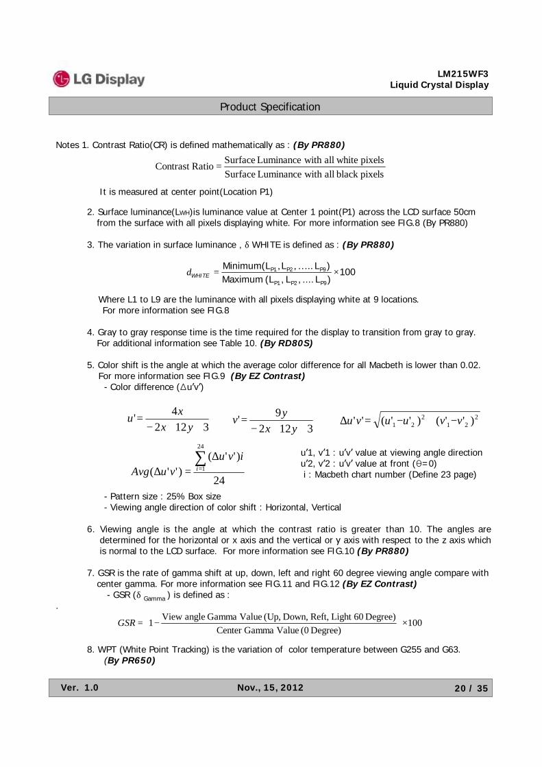
Notes 1. Contrast Ratio(CR) is defined mathematically as : (By PR880)
It is measured at center point(Location P1)
2. Surface luminance(LWH)is luminance value at Center 1 point(P1) across the LCD surface 50cm from the surface with all pixels displaying white. For more information see FIG.8 (By PR880)
3. The variation in surface luminance , δ WHITE is defined as : (By PR880)
Where L1 to L9 are the luminance with all pixels displaying white at 9 locations. For more information see FIG.8
4. Gray to gray response time is the time required for the display to transition from gray to gray. For additional information see Table 10. (By RD80S)
5. Color shift is the angle at which the average color difference for all Macbeth is lower than 0.02.For more information see FIG.9 (By EZ Contrast)- Color difference (Δu’v’)
u’1, v’1 : u’v’ value at viewing angle directionu’2, v’2 : u’v’ value at front (θ=0)i : Macbeth chart number (Define 23 page)
- Pattern size : 25% Box size- Viewing angle direction of color shift : Horizontal, Vertical
6. Viewing angle is the angle at which the contrast ratio is greater than 10. The angles aredetermined for the horizontal or x axis and the vertical or y axis with respect to the z axis whichis normal to the LCD surface. For more information see FIG.10 (By PR880)
7. GSR is the rate of gamma shift at up, down, left and right 60 degree viewing angle compare with center gamma. For more information see FIG.11 and FIG.12 (By EZ Contrast)
- GSR (δ Gamma ) is defined as : .
8. WPT (White Point Tracking) is the variation of color temperature between G255 and G63.(By PR650)
31224'
++−=
yxxu
31229'
++−=
yxyv 2
212
21 )''()''('' vvuuvu −+−=∆
pixelsblack all with Luminance Surfacepixels whiteall with Luminance SurfaceRatioContrast =
100)L .... ,L ,(L Maximum)L .. ,L,Minimum(L
P9P2P1
P9P2P1 ×…
=WHITEδ
24
)''()''(
24
1∑
=
∆=∆ i
ivuvuAvg
100Degree) (0 Value GammaCenter
Degree) 60Light Reft, Down, (Up, Value Gamma angle View1 ×
−=GSR
Product Specification
LM215WF3Liquid Crystal Display
Ver. 1.0 Nov., 15, 2012 21 / 35
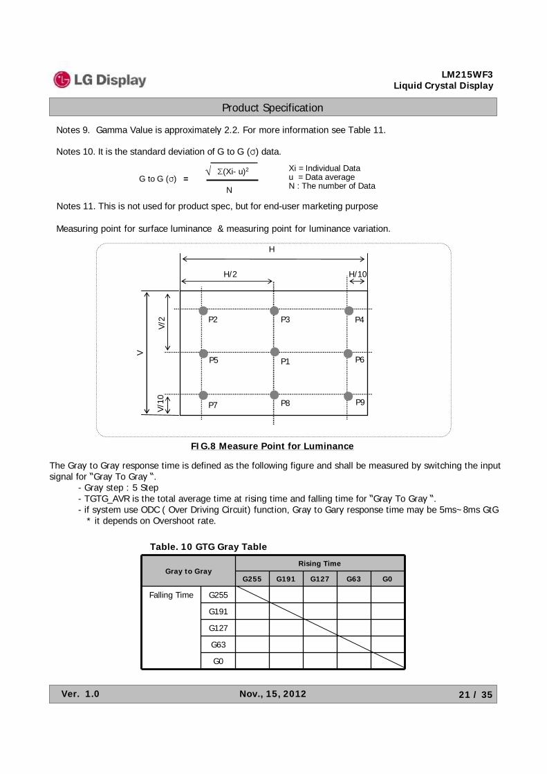
Table. 10 GTG Gray Table
Measuring point for surface luminance & measuring point for luminance variation.
H
H/2
V
V/2
●
P1
P4P2
P9P7
●
●
● ●
●P3
●P8
P6●P5●
H/10
V/10
Gray to GrayRising Time
G255 G191 G127 G63 G0
Falling Time G255
G191
G127
G63
G0
Notes 9. Gamma Value is approximately 2.2. For more information see Table 11.
The Gray to Gray response time is defined as the following figure and shall be measured by switching the input signal for “Gray To Gray “.
- Gray step : 5 Step - TGTG_AVR is the total average time at rising time and falling time for “Gray To Gray “.- if system use ODC ( Over Driving Circuit) function, Gray to Gary response time may be 5ms~8ms GtG
* it depends on Overshoot rate.
FIG.8 Measure Point for Luminance
Notes 10. It is the standard deviation of G to G (σ) data.
Notes 11. This is not used for product spec, but for end-user marketing purpose
Xi = Individual Datau = Data averageN : The number of Data
G to G (σ) = Σ(Xi- u)2
N
√
Product Specification
LM215WF3Liquid Crystal Display
Ver. 1.0 Nov., 15, 2012 22 / 35
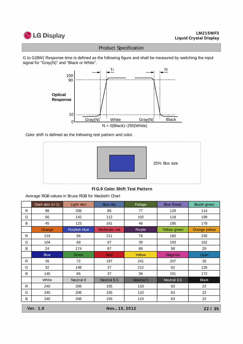
25% Box size
Dark skin (i=1) Light skin Blue sky Foliage Blue flower Bluish green
R 98 206 85 77 129 114
G 56 142 112 102 118 199
B 45 123 161 46 185 178
Orange Purplish blue Moderate red Purple Yellow green Orange yellow
R 219 56 211 76 160 230
G 104 69 67 39 193 162
B 24 174 87 86 58 29
Blue Green Red Yellow Magenta Cyan
R 26 72 197 241 207 35
G 32 148 27 212 62 126
B 145 65 37 36 151 172
White Neutral 8 Neutral 6.5 Neutral 5 Neutral 3.5 Black
R 240 206 155 110 63 22
G 240 206 155 110 63 22
B 240 206 155 110 63 22
Average RGB values in Bruce RGB for Macbeth Chart
Color shift is defined as the following test pattern and color.
FIG.9 Color Shift Test Pattern
WhiteGray(N)
Tr Tf10090
10
0
Optical Response
N = 0(Black)~255(White)Gray(N) Black
G to G(BW) Response time is defined as the following figure and shall be measured by switching the input signal for “Gray(N)” and “Black or White”.
Product Specification
LM215WF3Liquid Crystal Display
Ver. 1.0 Nov., 15, 2012 23 / 35
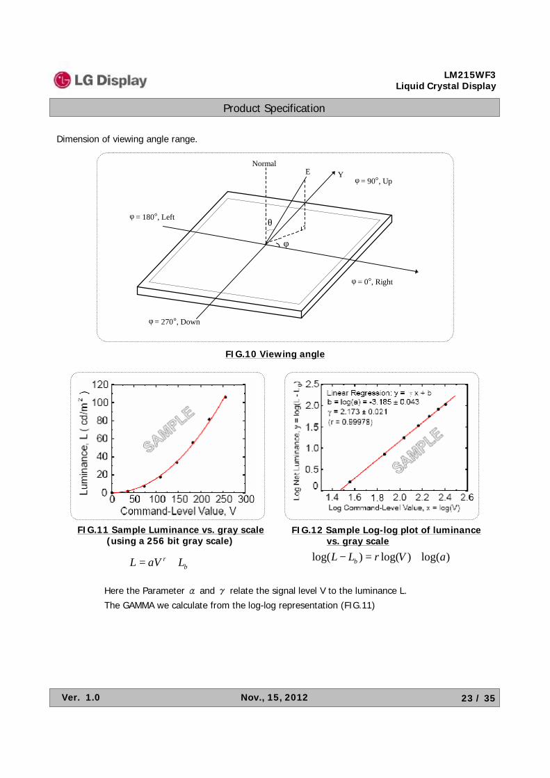
Dimension of viewing angle range.
Normal Y E
φ
θ
φ = 0°, Right
φ = 180°, Left
φ = 270°, Down
φ = 90°, Up
br LaVL += )log()log()log( aVrLL b +=−
Here the Parameter α and γ relate the signal level V to the luminance L.
The GAMMA we calculate from the log-log representation (FIG.11)
FIG.11 Sample Luminance vs. gray scale(using a 256 bit gray scale)
FIG.12 Sample Log-log plot of luminance vs. gray scale
FIG.10 Viewing angle
Product Specification
LM215WF3Liquid Crystal Display
Ver. 1.0 Nov., 15, 2012 24 / 35
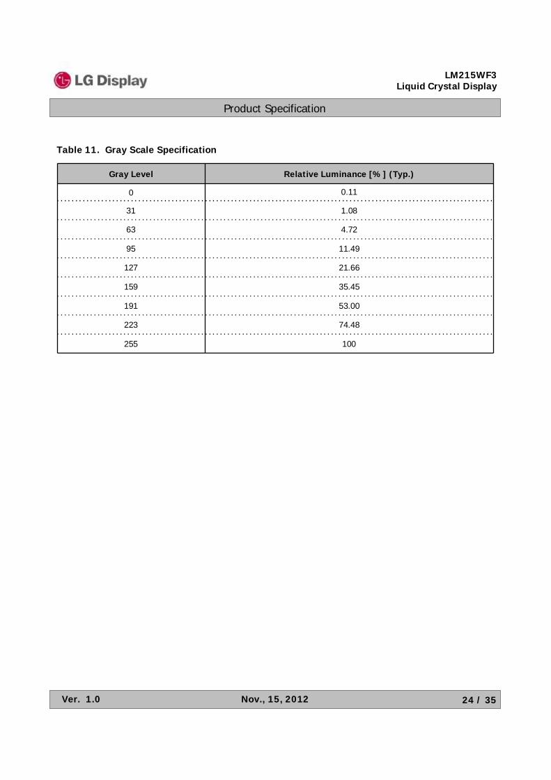
Table 11. Gray Scale Specification
Gray Level Relative Luminance [%] (Typ.)
0 0.11
31 1.08
63 4.72
95 11.49
127 21.66
159 35.45
191 53.00
223 74.48
255 100
Product Specification
LM215WF3Liquid Crystal Display
Ver. 1.0 Nov., 15, 2012 25 / 35
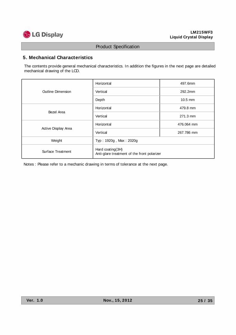
5. Mechanical Characteristics
The contents provide general mechanical characteristics. In addition the figures in the next page are detailed mechanical drawing of the LCD.
Notes : Please refer to a mechanic drawing in terms of tolerance at the next page.
Outline Dimension
Horizontal 497.6mm
Vertical 292.2mm
Depth 10.5 mm
Bezel AreaHorizontal 479.8 mm
Vertical 271.3 mm
Active Display AreaHorizontal 476.064 mm
Vertical 267.786 mm
Weight Typ : 1920g , Max : 2020g
Surface Treatment Hard coating(3H)Anti-glare treatment of the front polarizer
Product Specification
LM215WF3Liquid Crystal Display
Ver. 1.0 Nov., 15, 2012 26 / 35
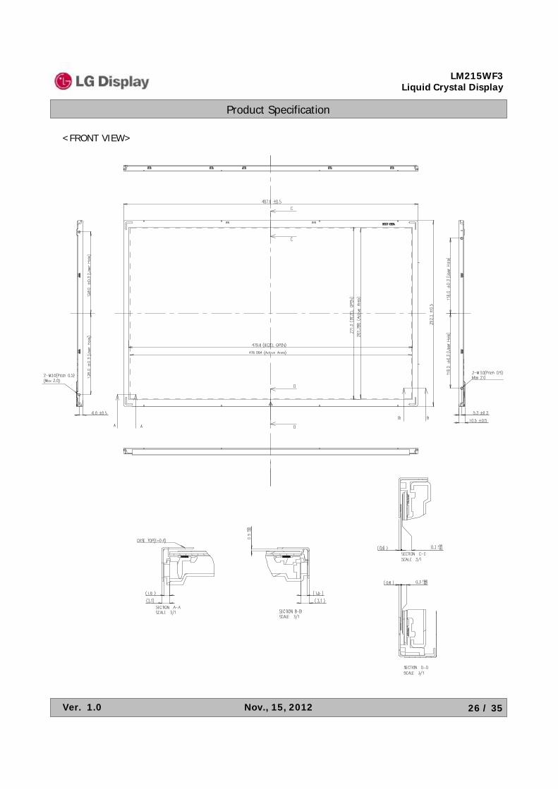
<FRONT VIEW>
Product Specification
LM215WF3Liquid Crystal Display
Ver. 1.0 Nov., 15, 2012 27 / 35
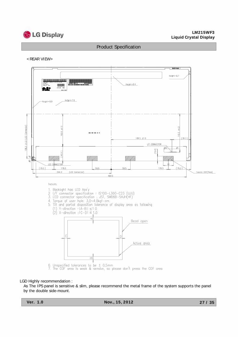
<REAR VIEW>
LGD Highly recommendation : As The IPS panel is sensitive & slim, please recommend the metal frame of the system supports the panelby the double side-mount.
Product Specification
LM215WF3Liquid Crystal Display
Ver. 1.0 Nov., 15, 2012 28 / 35
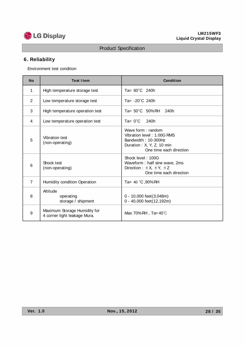
6. Reliability
Environment test condition
No Test Item Condition
1 High temperature storage test Ta= 60°C 240h
2 Low temperature storage test Ta= -20°C 240h
3 High temperature operation test Ta= 50°C 50%RH 240h
4 Low temperature operation test Ta= 0°C 240h
5 Vibration test(non-operating)
Wave form : randomVibration level : 1.00G RMSBandwidth : 10-300HzDuration : X, Y, Z, 10 min
One time each direction
6 Shock test(non-operating)
Shock level : 100GWaveform : half sine wave, 2msDirection :±X, ±Y, ±Z
One time each direction
7 Humidity condition Operation Ta= 40 °C ,90%RH
8Altitude
operatingstorage / shipment
0 - 10,000 feet(3,048m)0 - 40,000 feet(12,192m)
9 Maximum Storage Humidity for4 corner light leakage Mura. Max 70%RH , Ta=40℃
Product Specification
LM215WF3Liquid Crystal Display
Ver. 1.0 Nov., 15, 2012 29 / 35
7-3. Environment
a) RoHS, Directive 2002/95/EC of the European Parliament and of the council of 27 January 2003
7-2. EMC
a) ANSI C63.4 “American National Standard for Methods of Measurement of Radio-Noise Emissions from Low-Voltage Electrical and Electronic Equipment in the Range of 9 kHz to 40 GHz.”American National Standards Institute (ANSI), 2003.
b) CISPR 22 “Information technology equipment – Radio disturbance characteristics – Limit and methods of measurement." International Special Committee on Radio Interference (CISPR), 2005.
c) CISPR 13 “Sound and television broadcast receivers and associated equipment – Radio disturbance characteristics – Limits and method of measurement." International Special Committee on Radio Interference (CISPR), 2006.
7. International Standards
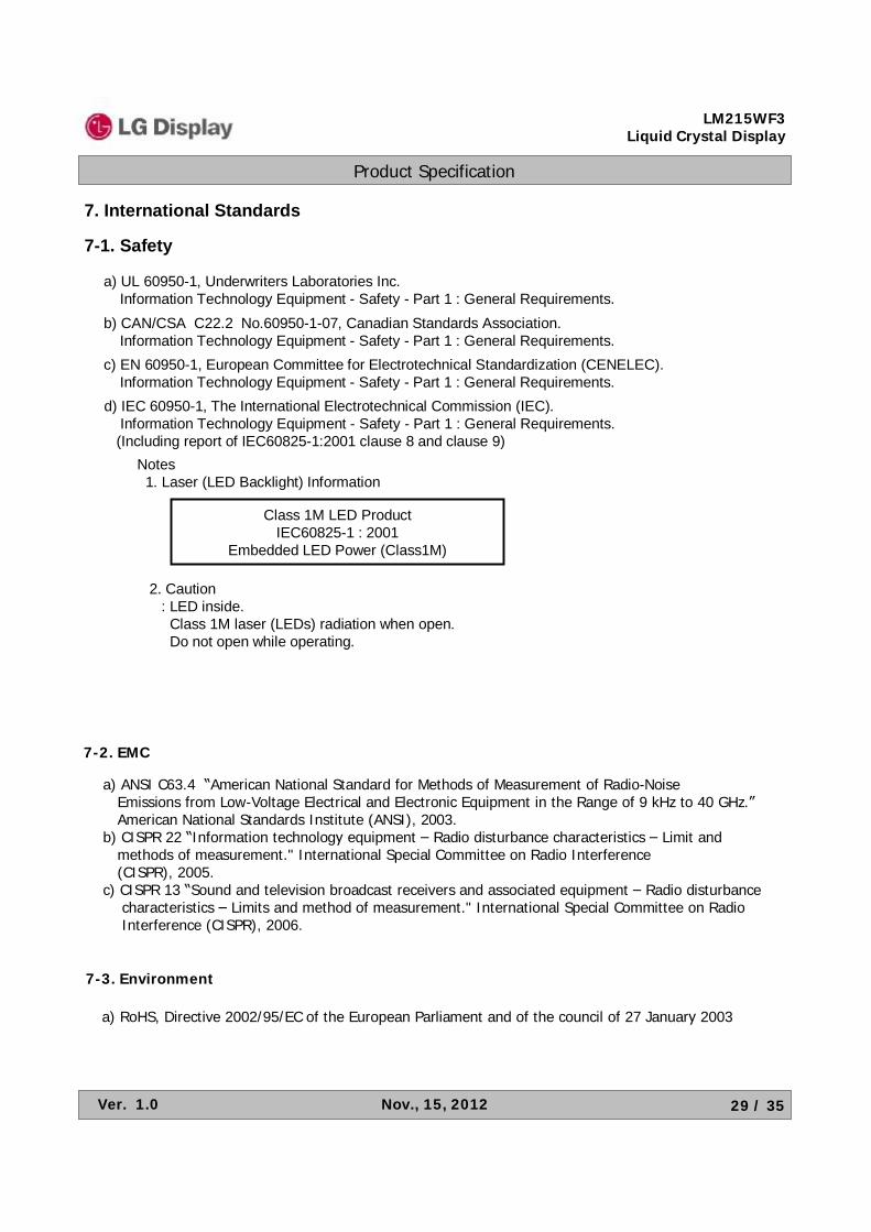
7-1. Safety
Class 1M LED ProductIEC60825-1 : 2001
Embedded LED Power (Class1M)
Notes 1. Laser (LED Backlight) Information
2. Caution: LED inside.
Class 1M laser (LEDs) radiation when open.Do not open while operating.
c) EN 60950-1, European Committee for Electrotechnical Standardization (CENELEC).Information Technology Equipment - Safety - Part 1 : General Requirements.
a) UL 60950-1, Underwriters Laboratories Inc.Information Technology Equipment - Safety - Part 1 : General Requirements.
b) CAN/CSA C22.2 No.60950-1-07, Canadian Standards Association.Information Technology Equipment - Safety - Part 1 : General Requirements.
d) IEC 60950-1, The International Electrotechnical Commission (IEC).Information Technology Equipment - Safety - Part 1 : General Requirements.(Including report of IEC60825-1:2001 clause 8 and clause 9)
Product Specification
LM215WF3Liquid Crystal Display
Ver. 1.0 Nov., 15, 2012 30 / 35
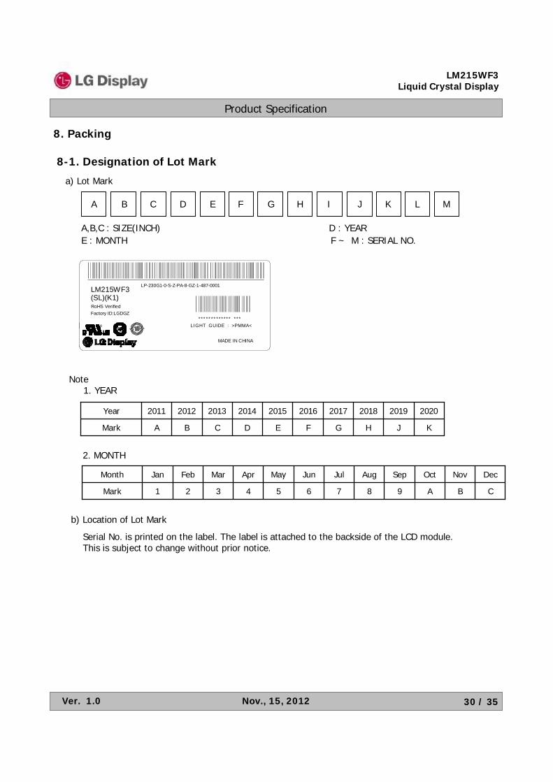
8. Packing
8-1. Designation of Lot Mark
a) Lot Mark
A B C D E F G H I J K L M
A,B,C : SIZE(INCH) D : YEAR E : MONTH F ~ M : SERIAL NO.
Note1. YEAR
2. MONTH
B
Nov
Mark
Month
A
Oct
6
Jun
7
Jul
8
Aug
9
Sep
4
Apr
5
May
C321
DecMarFebJan
b) Location of Lot Mark
Serial No. is printed on the label. The label is attached to the backside of the LCD module.This is subject to change without prior notice.
Mark
Year
K
2020
F
2016
G
2017
H
2018
J
2019
D
2014
E
2015
CBA
201320122011
LM215WF3(SL)(K1)
LP-230G1-0-S-Z-PA-8-GZ-1-487-0001
* * * * * * * * * * * * * * * *
MADE IN CHINA
LIGHT GUIDE : >PMMA<
RoHS VerifiedFactory ID:LGDGZ
Product Specification
LM215WF3Liquid Crystal Display
Ver. 1.0 Nov., 15, 2012 31 / 35
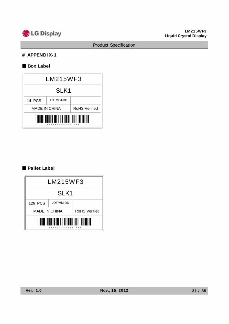
# APPENDIX-1
■ Box Label
■ Pallet Label
LM215WF3
SLK1LOT/MM-DD
MADE IN CHINA
* * * * * * * * * * * * * * * *
14 PCS
RoHS Verified
LM215WF3
SLK1LOT/MM-DD
MADE IN CHINA
* * * * * * * * * * * * * * * *
126 PCS
RoHS Verified
Product Specification
LM215WF3Liquid Crystal Display
Ver. 1.0 Nov., 15, 2012 32 / 35
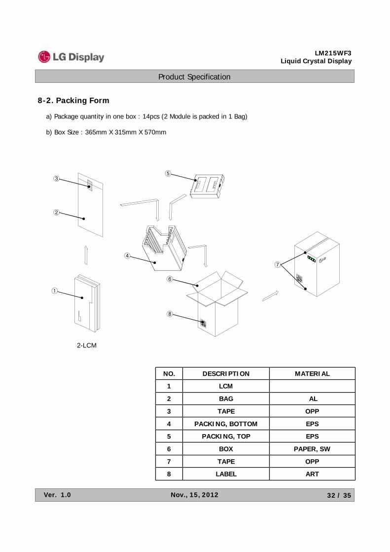
NO. DESCRIPTION MATERIAL
1 LCM
2 BAG AL
3 TAPE OPP
4 PACKING, BOTTOM EPS
5 PACKING, TOP EPS
6 BOX PAPER, SW
7 TAPE OPP
8 LABEL ART
a) Package quantity in one box : 14pcs (2 Module is packed in 1 Bag)
b) Box Size : 365mm X 315mm X 570mm
8-2. Packing Form
2-LCM
①
②
③
⑧
④
⑥
⑤
⑦
Product Specification
LM215WF3Liquid Crystal Display
Ver. 1.0 Nov., 15, 2012 33 / 35
8-3. Pallet Form
NO. DESCRIPTION MATERIAL
1 PACKING ASS’Y -
2 PALLET PLYWOOD_1140X990X117.5
3 BAND PP
4 CLIP, BAND STEEL
5 ANGLE, PACKING PAPER (SW)
6 LABEL PAPER
7 Wrapping LLDPE
Product Specification
LM215WF3Liquid Crystal Display
Ver. 1.0 Nov., 15, 2012 34 / 35
9. PRECAUTIONSPlease pay attention to the followings when you use this TFT LCD module.
9-1. MOUNTING PRECAUTIONS(1) You must mount a module using holes arranged in four corners or four sides.(2) You should consider the mounting structure so that uneven force (ex. Twisted stress) is not applied to the
module. And the case on which a module is mounted should have sufficient strength so that external force is not transmitted directly to the module.
(3) Please attach the surface transparent protective plate to the surface in order to protect the polarizer.Transparent protective plate should have sufficient strength in order to the resist external force.
(4) You should adopt radiation structure to satisfy the temperature specification.(5) Acetic acid type and chlorine type materials for the cover case are not desirable because the former
generates corrosive gas of attacking the polarizer at high temperature and the latter causes circuit break by electro-chemical reaction.
(6) Do not touch, push or rub the exposed polarizers with glass, tweezers or anything harder than HBpencil lead. And please do not rub with dust clothes with chemical treatment.Do not touch the surface of polarizer for bare hand or greasy cloth.(Some cosmetics are detrimentalto the polarizer.)
(7) When the surface becomes dusty, please wipe gently with absorbent cotton or other soft materials like chamois soaks with petroleum benzene. Normal-hexane is recommended for cleaning the adhesives used to attach front / rear polarizers. Do not use acetone, toluene and alcohol because they cause chemical damage to the polarizer.
(8) Wipe off saliva or water drops as soon as possible. Their long time contact with polarizer causes deformations and color fading.
(9) Do not open the case because inside circuits do not have sufficient strength. (10) As The IPS panel is sensitive & slim, please recommend the metal frame of the system supports the panel
by the double side-mount.
9-2. OPERATING PRECAUTIONS(1) The spike noise causes the mis-operation of circuits. It should be lower than following voltage :
V=±200mV(Over and under shoot voltage)(2) Response time depends on the temperature.(In lower temperature, it becomes longer.)(3) Brightness depends on the temperature. (In lower temperature, it becomes higher.)
And in lower temperature, response time(required time that brightness is stable after turned on) becomeslonger.
(4) Be careful for condensation at sudden temperature change. Condensation makes damage to polarizer or electrical contacted parts. And after fading condensation, smear or spot will occur.
(5) When fixed patterns are displayed for a long time, remnant image is likely to occur.(6) Module has high frequency circuits. Sufficient suppression to the electromagnetic interference shall be
done by system manufacturers. Grounding and shielding methods may be important to minimized theinterference.
(7) Please do not give any mechanical and/or acoustical impact to LCM. Otherwise, LCM can’t be operated its full characteristics perfectly.
(8) A screw which is fastened up the steels should be a machine screw. (if not, it causes metallic foreign material and deal LCM a fatal blow)
(9) Please do not set LCD on its edge.(10) When LCMs are used for public display defects such as Yogore, image sticking can not guarantee.(11) When this reverse model is used as a forward-type model (PCB on top side), LGD can not guarantee
any defects of LCM.(12) LCMs cannot support “Interlaced Scan Method”
Product Specification
LM215WF3Liquid Crystal Display
Ver. 1.0 Nov., 15, 2012 35 / 35
Since a module is composed of electronic circuits, it is not strong to electrostatic discharge. Make certain that treatment persons are connected to ground through wrist band etc. And don’t touch interface pin directly.
9-3. ELECTROSTATIC DISCHARGE CONTROL
Strong light exposure causes degradation of polarizer and color filter.
9-4. PRECAUTIONS FOR STRONG LIGHT EXPOSURE
When storing modules as spares for a long time, the following precautions are necessary.
(1) Store them in a dark place. Do not expose the module to sunlight or fluorescent light. Keep the temperature between 5°C and 35°C at normal humidity.
(2) The polarizer surface should not come in contact with any other object.It is recommended that they be stored in the container in which they were shipped.
9-5. STORAGE
9-6. HANDLING PRECAUTIONS FOR PROTECTION FILM
(1) The protection film is attached to the bezel with a small masking tape.When the protection film is peeled off, static electricity is generated between the film and polarizer.This should be peeled off slowly and carefully by people who are electrically grounded and with well ion-blown equipment or in such a condition, etc.
(2) When the module with protection film attached is stored for a long time, sometimes there remains a very small amount of glue still on the bezel after the protection film is peeled off.
(3) You can remove the glue easily. When the glue remains on the bezel surface or its vestige is recognized, please wipe them off with absorbent cotton waste or other soft material like chamois soaked with normal-hexane.