Embed Size (px)
Citation preview
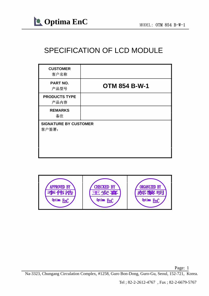
MODEL: OTM 854 B-W-1Optima EnC
SPECIFICATION OF LCD MODULE
CUSTOMER客户名称
PART NO.产品型号 OTM 854 B-W-1
PRODUCTS TYPE产品内容
REMARKS备注
SIGNATURE BY CUSTOMER客户签署:
1Page:Na-3323, Chungang Circulation Complex, #1258, Guro Bon-Dong, Guro-Gu, Seoul, 152-721, Korea.
Tel ; 82-2-2612-4767 , Fax ; 82-2-6679-5767
MODEL: OTM 854 B-W-1Optima EnC
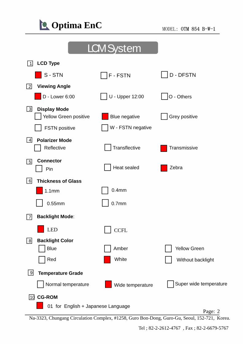
LCM System
2
LCD Type
S - STN F - FSTN
Viewing Angle
D - DFSTN
LCM System1
3
U - Upper 12:00D - Lower 6:00 O - Others
Display ModeYellow Green positive Blue negative Grey positive
FSTN positive W - FSTN negative
4
5
Polarizer ModeReflective TransmissiveTransflective
ConnectorPin Heat sealed Zebra
Thickness of Glass
1.1mm 0.4mm
0.55mm 0.7mm
6
7
8 Backlight ColorBlue Amber Yellow Green
Backlight Mode:
CCFLLED
Red White Without backlight
Temperature Grade
Wide temperatureNormal temperature Super wide temperature
9
2Page:Na-3323, Chungang Circulation Complex, #1258, Guro Bon-Dong, Guro-Gu, Seoul, 152-721, Korea.
Tel ; 82-2-2612-4767 , Fax ; 82-2-6679-5767
10 CG-ROM
01 for English + Japanese Language
MODEL: OTM 854 B-W-1Optima EnC
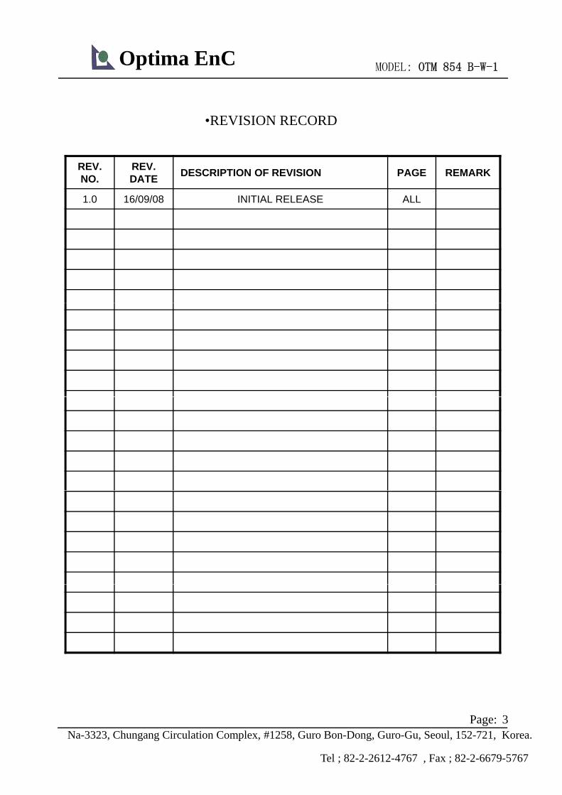
REVISION RECORD
REV. NO.
REV. DATE DESCRIPTION OF REVISION PAGE REMARK
1.0 16/09/08 INITIAL RELEASE ALL
•REVISION RECORD
3Page:Na-3323, Chungang Circulation Complex, #1258, Guro Bon-Dong, Guro-Gu, Seoul, 152-721, Korea.
Tel ; 82-2-2612-4767 , Fax ; 82-2-6679-5767

MODEL: OTM 854 B-W-1Optima EnC
CONTENTS1. FEATURES ……………………………………………...........................….
2. MECHANICAL DATA ……………………………………………………..….
5
5
3. ABSOLUTE MAXIMUM RATING ………………………..………………….
4. ELECTRICAL CHARACTERISTICS …..………………………………… …
5. ELECTRO-OPTICAL CHARACTERISTICS .…………...………………….
6
8
10
6. BLOCK DIAGRAM ..……………………………………………………….…
7. POWER SUPPLY …………………..………………………………………..
8. TIMIING DIAGRAM ……………………………….…..………….………....
11
11
12
9. AC CHARACTERISTICS…………………………………………………….
10. INITIALIZATION SEQUENCE ……..…………….………………………...
11. INSTRUCTION SET ……………………………….………………………...
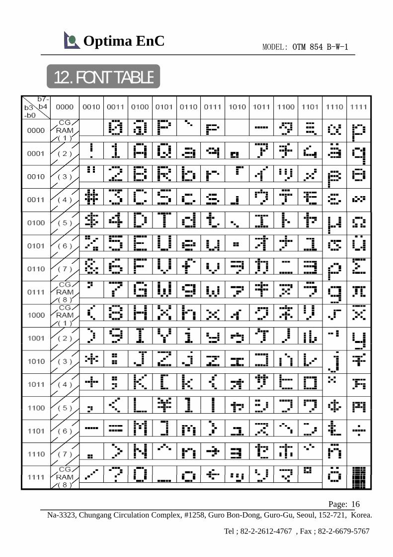
12 FONT TABLE
13
14
15
12. FONT TABLE…..……..……..………………………………………….…….
13. QUALITY ASSURANCE………………………………………………………
14. OUTLINE DRAWING .....……..…………………..…………….…………..
15 INTERFACE
16
17
21
2215. INTERFACE .....……..…………………………….…………………………..
16. PACKAGE INFORMATION…………………………………………………..
17. QC/QA PROCEDURE ......………………………………...………………...
18. HANDING PRECAUTIONS…………………………………………………..
22
23
24
25
4Page:Na-3323, Chungang Circulation Complex, #1258, Guro Bon-Dong, Guro-Gu, Seoul, 152-721, Korea.
Tel ; 82-2-2612-4767 , Fax ; 82-2-6679-5767


MODEL: OTM 854 B-W-1Optima EnC
3 ABSOLUTE MAXIMUM RATINGS3. ABSOLUTE MAXIMUM RATINGS
(TA = 25 , Vss=0V)3.1 Electrical Absolute Maximum Rating
Item Symbol MIN. Max. Unit
Supply Voltage (Logic) VDD-VSS 0 7.0 V
Supply Voltage (LCD Driveer)
VLCD VDD-12 VDD+0.3 V
Input Voltage VIN -0.3 VDD+0.3 V
3 2 Environmental Absolute Maximum Rating
Input Voltage VIN 0.3 VDD 0.3 V
Operating temperature Top -20 70 ℃
Storage temperature Tsto -30 80 ℃
3.2 Environmental Absolute Maximum Rating
ItemOperating Storage
CommentMin. Max. Min. Max.
Ambient temp -20 +70 -30 +80 Note(1)
Humidity Note(2) Note(2) Without condensation
Vibration -- 4.9M/S2 -- 19.6M/S2 XYZ direction
Shock -- 29.4M/S2 -- 490M/S2 XYX direction
Note(1) Ta=0℃: 50 Hr Max.Note(2) Ta 40℃: 90%RH Max.
Ta 40℃: Absolue humidity must be lower than the humidity of 90%RH@40℃Ta 40℃: Absolue humidity must be lower than the humidity of 90%RH@40℃
6Page:Na-3323, Chungang Circulation Complex, #1258, Guro Bon-Dong, Guro-Gu, Seoul, 152-721, Korea.
Tel ; 82-2-2612-4767 , Fax ; 82-2-6679-5767

MODEL: OTM 854 B-W-1Optima EnC
3.3 Electronic Static Discharge Maximum RatingESD T t M th d IEC 1000 4 2ESD Test Method : IEC-1000-4-2
Item Description
Testing environment Ambient temperature : 15℃ to 35℃Humidity : 30% to 60%LCM(E.U.T) : Power up
Testing equipment Manufacture : Noiseken, Model No. ESD
Testing condition See drawing 1
Direct discharge 0 to ± 4KV Discharge point, see drawing2
Indirect discharge 0 to ± 8KV Discharge point, see drawing1
Pass condition No malfunction of unit. Temporary malfunction of unitwhich can be recovered by system reset.
Fail condition Non. Recoverable malfunction of LCM or system.
FIG1 ESD Testing Equipment
Direct Contact Discharge / Contact Point : A,B,C,D
7Page:Na-3323, Chungang Circulation Complex, #1258, Guro Bon-Dong, Guro-Gu, Seoul, 152-721, Korea.
Tel ; 82-2-2612-4767 , Fax ; 82-2-6679-5767

MODEL: OTM 854 B-W-1Optima EnC
4. ELECTRICAL CHARACTERISTICS4. ELECTRICAL CHARACTERISTICS(VDD = 4.5 to 5.5V , TA = 25 )
8Page:Na-3323, Chungang Circulation Complex, #1258, Guro Bon-Dong, Guro-Gu, Seoul, 152-721, Korea.
Tel ; 82-2-2612-4767 , Fax ; 82-2-6679-5767

MODEL: OTM 854 B-W-1Optima EnC
4.1 LED ELECTRICAL/OPTLCAL CHARACTERISTICSItem Symbol min typ max Unit Condition
Forward Voltage Vf 4.8 5.0 5.2 V If= 120 mA
Reverse Current Ir 120 uA Vr=5V
Dominant wave length λp - - - nm If= mA
4.2 LED ABSOLUTE MAXIMUM RATINGS
Luminance Lv 200 250 - cd/㎡ If= 120 mA
Chromaticity Coordinates XY - 0.29
0.30 - - If= 120 mA
Item Symbol Condition Rating Unit
Reverse Voltage Vr Ta=25℃ 5 V
Absolute maximum forward current Ifm Ta=25℃ 160 mA
Power description pd Ta=25℃ 800 mW
4.2.1 LED ARRAY BLOCK DIAGRAM ( LED DICE = 4 dices )
D1
D2
LEDA LEDKR
D2
D3
D4
4.2.2 LED POWER SOURCE
LED
Option Power source Jumper settingA 15A/16K R9、R11-R13B 15K/16A R8、R10、R12、R13
C VDD/VSS R12 R15
9Page:Na-3323, Chungang Circulation Complex, #1258, Guro Bon-Dong, Guro-Gu, Seoul, 152-721, Korea.
Tel ; 82-2-2612-4767 , Fax ; 82-2-6679-5767
C VDD/VSS R12-R15
GND FRM GND R16

MODEL: OTM 854 B-W-1Optima EnC
5. ELECTRO-OPTICAL CHARACTERISTICS5 C O O C C C S CS
ITEM SYMBOL CONDITION MIN.
TYP.MAX. UNIT NOT
E
Contrast ratio K φ=0 1.4 4 - - 1
Response time Tr 1 - 130 - ms 2Response time (rise)
Tr φ=1 130 ms 2
Response time (fall) Tf φ=2 130 - ms 2
Viewing angleφ
K ≥1.4-40 -- +10
deg. 3θ -30 -- +30
Note 1: Definition of Contrast Ratio “K”
Note 2: Definition of OpticalResponse Time
K=
90%Brightness Curve ofselected area
Brightness of non-selected segment(A)
A
Brightness of selected segment(B)
10%
Brightness Curve ofnon-selected area
Vop Driving Voltage
Brig
htne
s s
B
Non-selected Selected Non-selected
100%
0%Brightness 90%
10%
Rise Time Fall Time
∅ ∅
Left Right
Top
Note 3: Definition of Viewing Angle
Vop Driving Voltage Rise Time Fall Time
θ
θ
∅ ∅Top
Bottom
Viewing Surface
pViewing Angle
Viewing AngleBottom
10Page:Na-3323, Chungang Circulation Complex, #1258, Guro Bon-Dong, Guro-Gu, Seoul, 152-721, Korea.
Tel ; 82-2-2612-4767 , Fax ; 82-2-6679-5767
Please select either top or bottom viewing angle

MODEL: OTM 854 B-W-1Optima EnC
6 BLOCK DIAGRAM6. BLOCK DIAGRAM
CONTROLLER:VSS LCDCOM 1-16
SEG 121-200
CONTROLLER:
SPLC 780D
OR
VSSVDDVEE
RSR/W
D0 D7
E
20 character×4 line
SEGMENT
SEG 1-40
SEG 41-120
4 SEGMENT
7. POWER SUPPLY
EequivalenceD0~D7 SEGMENT
DRIVER4 SEGMENT
DRIVER
7. POWER SUPPLY
11Page:Na-3323, Chungang Circulation Complex, #1258, Guro Bon-Dong, Guro-Gu, Seoul, 152-721, Korea.
Tel ; 82-2-2612-4767 , Fax ; 82-2-6679-5767

MODEL: OTM 854 B-W-1Optima EnC
8 TIMING DIAGRAM
• WRITE OPERATION
8. TIMING DIAGRAM
• READ OPERATION
12Page:Na-3323, Chungang Circulation Complex, #1258, Guro Bon-Dong, Guro-Gu, Seoul, 152-721, Korea.
Tel ; 82-2-2612-4767 , Fax ; 82-2-6679-5767

MODEL: OTM 854 B-W-1Optima EnC
9 AC CHARACTERISTICS9. AC CHARACTERISTICS
• WRITE MODE
READ MODE• READ MODE
13Page:Na-3323, Chungang Circulation Complex, #1258, Guro Bon-Dong, Guro-Gu, Seoul, 152-721, Korea.
Tel ; 82-2-2612-4767 , Fax ; 82-2-6679-5767

MODEL: OTM 854 B-W-1Optima EnC
10. INITIALIZATION SEQUENCE10. INITIALIZATION SEQUENCE
14Page:Na-3323, Chungang Circulation Complex, #1258, Guro Bon-Dong, Guro-Gu, Seoul, 152-721, Korea.
Tel ; 82-2-2612-4767 , Fax ; 82-2-6679-5767

MODEL: OTM 854 B-W-1Optima EnC
11. INSTRUCTION SET11. INSTRUCTION SET
COMMANDCOMMAND CODE
RS R/W DB7 DB6 DB5 DB4 DB3 DB2 DB1 DB0COMMAND CODE
Screen Clear, Set AC to 0Cursor Reposition
E-CYCLEfosc=250KHz
1.64msSCREENCLEAR 0 0 0 0 0 0 0 0 0 1
DDRAM AD 0 R tCURSOR DDRAM AD=0, Return,Content Changeless 1.64msCURSOR
RETURN 0 0 0 0 0 0 0 0 1 *
Set moving direction of cursor,Appoint if move 40usINPUT SET 0 0 0 0 0 0 0 1 I/D S
Set display on/off,cursor on/off,blink on/off 40usDISPLAY
SWITCH 0 0 0 0 0 0 1 D C B
Remove cursor and whole 40usSHIFT 0 0 0 0 0 1 S/C R/L * * display,DDRAM changeless 40usSHIFT 0 0 0 0 0 1 S/C R/L * *
Set DL,display line,font 40usFUNCTIONSET 0 0 0 0 1 DL N F * *
Set CGRAM AD,send receive data 40usCGRAM
AD SET 0 0 0 1 ACG
Set DDRAM AD,send receive data 40usDDRAM
AD SET 0 0 1 ADD send receive dataAD SETExecuting internal function,
reading AD of CT 40usBUSY/ADREAD CT 0 1 BF AC
Write data from CGRAM or DDRAM 40us
CGRAM/DDRAM
DATA WRITE1 0 DATA WRITE
Read data from CGRAM orDDRAM 40us
CGRAM/DDRAM 1 1 DATA READ DDRAMDATA READ
DDRAM: Display data RAMCGRAM: Character
Generator RAMACG: CGRAM ADADD: DDRAM AD & Cursor
E-cyclechangingwith mainfrequency.Example:If fcp or
I/D=1: Increment Mode; I/D=0: Decrement ModeS=1: ShiftS/C=1: Display Shift; S/C=0: Cursor ShiftR/L=1: Right Shift; R/L=0: Left ShiftDL=1: 8D DL=0: 4D ADD: DDRAM AD & Cursor
ADAC: Address counter for
DDRAM & CGRAM
If fcp or fosc=270KHz
40us x250/270=37us
N=1: 2R N=0: 1RF=1: 5x10 Style; F=0: 5x7 StyleBF=1: Execute Internal Function;BF=0: Command Received
15Page:Na-3323, Chungang Circulation Complex, #1258, Guro Bon-Dong, Guro-Gu, Seoul, 152-721, Korea.
Tel ; 82-2-2612-4767 , Fax ; 82-2-6679-5767
MODEL: OTM 854 B-W-1Optima EnC
12. FONT TABLE12. FONT TABLE
16Page:Na-3323, Chungang Circulation Complex, #1258, Guro Bon-Dong, Guro-Gu, Seoul, 152-721, Korea.
Tel ; 82-2-2612-4767 , Fax ; 82-2-6679-5767

MODEL: OTM 854 B-W-1Optima EnC
13. QUALITY ASSURANCEQ13.1.1 Temperature and Humidity(Ambient Temperature)
Temperature : 20 ± 5°CHumidity : 65 ± 5%
131.1.2 OperationUnless specified otherwise test will be conductedUnless specified otherwise, test will be conducted under function state.
13.1.3 ContainerUnless specified otherwise, vibration test will be conducted to the product itself without putting it in a container.
13.1.4 Test FrequencyIn case of related to deterioration such as shock test.It will be conducted only once.
13.1.5 Test Method
No. Parameter Conditions Regulations
1 High Temperature Operating 70±2℃ Note 3
2 Low Temperature Operating -20 ±2℃ Note 3
3 High Temperature Storage 80±2℃ Note 3
4 Low Temperature Storage -30±2℃ Note 34 Low Temperature Storage -30±2℃ Note 3
5 Vibration Test (Non-operation state)
Total fixed amplitude : 1.5mmVibration Frequency : 10 ~ 55Hz
One cycle 60 seconds to 3 directionsof X.Y.Z. for each 15 minutes
Note 3
6 Damp Proof Test (Non-operation state) 40℃±2℃, 90~95%RH, 96h Note 1,2
7 Shock Test (Non-operation state)
To be measured after dropping from 60cm high once concrete surface in packing state
Note 3
Note 1: Returned under normal temperature and humidity for 4 hrs.Note 2: No dew condensation to be observed.
h di l d i i d h di i
17Page:Na-3323, Chungang Circulation Complex, #1258, Guro Bon-Dong, Guro-Gu, Seoul, 152-721, Korea.
Tel ; 82-2-2612-4767 , Fax ; 82-2-6679-5767
Note 3: No change on display and in operation under the test condition

MODEL: OTM 854 B-W-1Optima EnC
13.2Inspection condition
13.2.1 Inspection conditionsThe LCD shall be inspected under 40W white fluorescent light.
13.2.2 Definition of applicable Zones13.2.2 Definition of applicable Zones
18Page:Na-3323, Chungang Circulation Complex, #1258, Guro Bon-Dong, Guro-Gu, Seoul, 152-721, Korea.
Tel ; 82-2-2612-4767 , Fax ; 82-2-6679-5767

MODEL: OTM 854 B-W-1Optima EnC
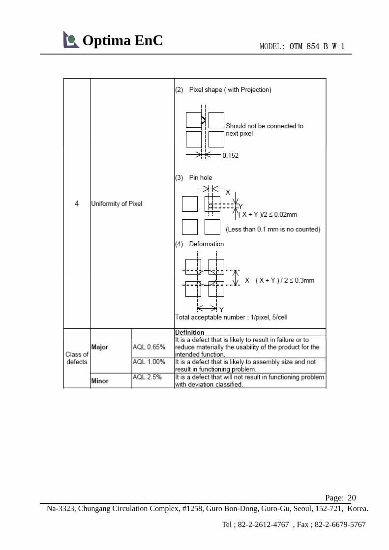
13.2.3 Inspection Parameters
19Page:Na-3323, Chungang Circulation Complex, #1258, Guro Bon-Dong, Guro-Gu, Seoul, 152-721, Korea.
Tel ; 82-2-2612-4767 , Fax ; 82-2-6679-5767
MODEL: OTM 854 B-W-1Optima EnC
20Page:Na-3323, Chungang Circulation Complex, #1258, Guro Bon-Dong, Guro-Gu, Seoul, 152-721, Korea.
Tel ; 82-2-2612-4767 , Fax ; 82-2-6679-5767

MODEL: OTM 854 B-W-1Optima EnC
14 OUTLINE DRAWING14. OUTLINE DRAWING
1 2 3 4 5 6 7 8VSS VDD V0 RS R/W E DB0 DB1
9 10 11 12 13 14 15 16DB2 DB3 DB4 DB5 DB6 DB7 LEDA LEDK
21Page:Na-3323, Chungang Circulation Complex, #1258, Guro Bon-Dong, Guro-Gu, Seoul, 152-721, Korea.
Tel ; 82-2-2612-4767 , Fax ; 82-2-6679-5767

MODEL: OTM 854 B-W-1Optima EnC
15 INTERFACE15. INTERFACE
PIN NO. SYMBOL DESCRIPTION FUNCTION1 VSS GROUND 0V (GND)
2 VDD POWER SUPPLY FOR LOGIC +5V2 VDDCIRCUIT
+5V
3 V0 LCD CONTRASTADJUSTMENT
4 RS INSTRUCTION/DATAREGISTER SELECTION
RS = 0 : INSTRUCTION REGISTERRS = 1 : DATA REGISTER
5 R/W READ/WRITE SELECTION R/W = 0 : REGISTER WRITER/W = 1 : REGISTER READ
6 E ENABLE SIGNAL7 DB08 DB19 DB210 DB311 DB412 DB513 DB6
DATA BUS 8 BIT: DB0-DB7
14 DB7
15 LEDASUPPLY VOLTAGE FORLED+ +5V
16 LEDK SUPPLY VOLTAGE FOR LED- 0V
22Page:Na-3323, Chungang Circulation Complex, #1258, Guro Bon-Dong, Guro-Gu, Seoul, 152-721, Korea.
Tel ; 82-2-2612-4767 , Fax ; 82-2-6679-5767

MODEL: OTM 854 B-W-1Optima EnC
16. PACKAGE INFORMATIONA Box include 50pcs
Modul e
Ant i - st at i c Bag
23Page:Na-3323, Chungang Circulation Complex, #1258, Guro Bon-Dong, Guro-Gu, Seoul, 152-721, Korea.
Tel ; 82-2-2612-4767 , Fax ; 82-2-6679-5767

MODEL: OTM 854 B-W-1Optima EnC
17 QC/QA PROCEDURE17. QC/QA PROCEDURE
Parts QA Dept. LCD Mfg. Dept. LCM QA Dept.Parts
1 Function & Appearance &
Soldering
Parts AcceptanceInspection
1. Function & Appearance &Dimension: Sample Test
2. Reliability: Random Sampling
Soldering Inspection
LCM Assembling
Soldering Condition
1. Dimension: Sample Test2. Function: 100% Inspection
-10~70℃ (1 Cycle=6 Hrs)
High Temp. Test
Heat Cycle Aging -10 70℃ (1 Cycle=6 Hrs).2 Cycle: 100% Inspection
Function & Appearance:100% Inspection (ex. 50℃)
1. Function & Appearance:Inspection
O t i I ti
Packaging
pp100% Inspection
2. Dimension: Random Sampling
Package Condition & Label:100% Inspection
Storage/Shipping
Outgoing Inspection1. Function,Appearance &
Dimension: Random Sampling2. Package Product & Label:
Random Sampling3.Electro-optical Characteristic:
100% Inspection4. Reliability: Random Sampling
24Page:Na-3323, Chungang Circulation Complex, #1258, Guro Bon-Dong, Guro-Gu, Seoul, 152-721, Korea.
Tel ; 82-2-2612-4767 , Fax ; 82-2-6679-5767

MODEL: OTM 854 B-W-1Optima EnC
18 Handling Precautions18. Handling Precautions1. Limitation of Application:Optrex products are designed for use in ordinary electronic devices such as business machines, telecommunications equipment,measurement devices and etc. Please handle the products with care. (see below)Optrex products are not designed,intended ,or authorized for use in any application which the failure of the product couldresult in a situation where personal injury or death may occur . these applications include, but are not limited to . life-sustaining equipment,nuclear control devices , aerospace equipment , devices related to hazardous or flammable materials , etc.[If Buyer intends to purchase or use the Optrex Products for such unintended or unauthorized applications Buyer must secure priorintends to purchase or use the Optrex Products for such unintended or unauthorized applications , Buyer must secure priorwritten consent to such use by a responsible officer of Optrex Corporation.]Should Buyer purchase or use Optrex Products for any such unintended or unauthorized application [ without such consent ].Buyer shall indemnify and hold Optrex and its officers.employees. subsidiaries, affiliates and distributors harmless against all claims, costs, damages and expenses , and reasonableattorney’s fees,arising out of , directly or indirectly, any claim of personal injury or death associated with such unintended or unauthorized use, even if such claim alleges that Optrex was negligent regarding the design or manufacture of the part.2.Industrial Rights and Patents Optrex shall not be responsible for any infringement of industrial property rights of third parties in any country arising out of theapplication or use of Optrex products, except which directly concern the structure or production of such products.pp p p , p y p p
No Press and Shock! Don’t Swallow or Touch Liquid Crystal!
If pressure to LCD, orientation may be disturbed.
LCD will broken by shock!
Liquid Crystal may be leaked when display is broked.
If it accidentally gets your hands,wash then with water!
Don’t not Scratch! No DC Voltage to LCD!
DC
Polarizer is a soft material and can easily be scratched.
No!
DC volrage or driveing higherthan the specified voltagewill reduce the lifetime ofthe LCD.
25Page:Na-3323, Chungang Circulation Complex, #1258, Guro Bon-Dong, Guro-Gu, Seoul, 152-721, Korea.
Tel ; 82-2-2612-4767 , Fax ; 82-2-6679-5767

MODEL: OTM 854 B-W-1Optima EnC
Don’t Press the Metallic Frame and Disassemble Slowly Peel Off Protective Film!
Pressure on the metallic frame and PCB may deformthe conductive rubber or break the liquid crystalcell and back light, whichwill cause defects
Don t Press the Metallic Frame and Disassemblethe LCM
Avoid static electricity.
Slowly Peel Off Protective Film!
be reshaped, which willconductive rubber may
LCD may be shifted or
cause defects.
will cause defects.
Avoid Static Electricity! Wear Gloves While Handing!
Please be sure to groundhuman body and electricapploances during work.
It is preferable to useconductive mat on table
Avoid Static Electricity! Wear Gloves While Handing!
It is preferable to wear glovesto avoid damaging the LCD.
Please do not touch electrodeswith bare hands or makethem dirtyand wear cotton clothes
or conduction processedfiber. Synthetic fiber isnot recommended.
Keep Away From Extreme Heat and Humidity! Use Alcohol to Clean Terminals!
GLOVE
them dirty.
LCD deteriorates.
p y y
When attaching with theheat seal or anisontropicallyconductive film wipe off
Alcohol
conductive film, wipe offwith alcohol before use.
26Page:Na-3323, Chungang Circulation Complex, #1258, Guro Bon-Dong, Guro-Gu, Seoul, 152-721, Korea.
Tel ; 82-2-2612-4767 , Fax ; 82-2-6679-5767

MODEL: OTM 854 B-W-1Optima EnC
Don’t Drop Water on LCD! Note that the presence of
waterdrops or dew in theLCD panel may deteriorate the polarizer or corradeelectrode.
o t op ate o C
Precaution in Soldering LCD Module
Basic instructions: Solder I/O terminals only.Use soldering iron without leakage.(1)Soldering condition to I/O terminals(1)Soldering condition to I/O terminals
Temperature at tip of the iron: 280±10℃Soldering time: 3~4 sec.Type of solder: Eutectic solder (containing colophony-flux)*Please do not use flux because it may soak into LCD Module or contaminate it.*It is preferable to peel off protective film on display surface after soldering I/Oterminals is finished.
(2)Remove connector or cable( )*When you remove connector or cable soldered to I/O terminals, please confirm that solder is fully melted. If you remove by force, electrodes at I/O terminals maybe damaged(or stripped off).*It is recommended to use solder suction machine.
Long-term Storage
If it is necessary to store LCD modules for a long time, please comply with thefollowing procedures.If storage condition is not satisfactory, display(especially polarizer) may be deterioratedor soldering I/O terminals may become difficult(some oxide is generated at I/Oterminals plating).1.Store as delivered by Optrex2 If you store as unpacked put in anti-static bag seal its opening and store where it is2.If you store as unpacked,put in anti static bag,seal its opening and store where it isnot subjected to direct sunshine nor fluorescent lamp.
3.Store at temperature 0 to +35℃ and at low humidity.Please refer to our specificationsheets for storage temperature range and humidity condition.
Long-term StoragePlease use power supply with built-in surge protection circuit.
27Page:Na-3323, Chungang Circulation Complex, #1258, Guro Bon-Dong, Guro-Gu, Seoul, 152-721, Korea.
Tel ; 82-2-2612-4767 , Fax ; 82-2-6679-5767