Embed Size (px)
Citation preview

Nios II Embedded Processor Design Contest—Outstanding Designs 2005
74
Third Prize
Spectral Estimation Using a MUSIC Algorithm
Institution: Indian Institute of Technology, Kanpur
Participants: Jawed Qumar
Instructor: Baquer Mazhari
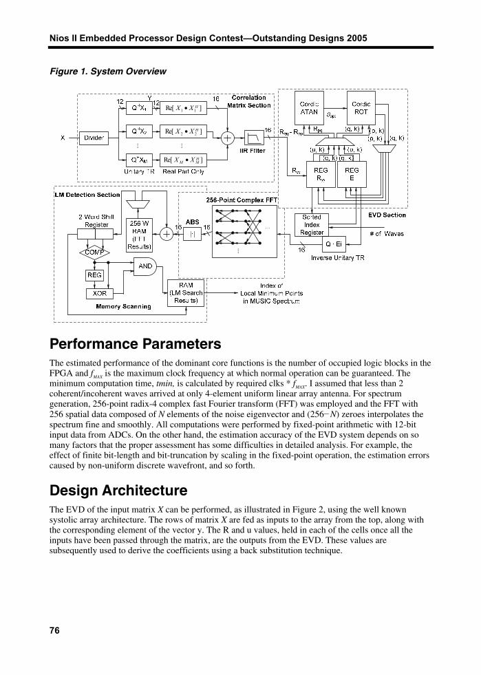
Design Introduction I have implemented a high resolution spectral estimation multiple signal classification (MUSIC) algorithm in an Altera® Stratix® FPGA. MUSIC detects signal frequencies by performing an eigen decomposition on the data vector covariance matrix from received signal samples. High-resolution spectral estimation is a major challenge of any advanced Doppler radar, cellular mobile base stations, etc. Eigen value decomposition (EVD) and MUSIC temporal spectra computations with a cyclic Jacobi processor based on a Coordinate Rotation Digital Computer (CORDIC), is the major signal processing being implemented using an Altera Stratix FPGA. All the digital signal processing (DSP) functions are based on fixed-point arithmetic and are well suited for the Stratix FPGA architecture. The feature-rich Sratix FPGA is armed with a Nios® II processor that has custom instruction and multi-mastering capabilities, as well as a powerful system development platform: SOPC Builder. The Nios II processor integrated development environment (IDE) has made the FPGA an attractive alternative to implement algebraic signal processing algorithms.
Spectral Estimation Using a MUSIC Algorithm
75
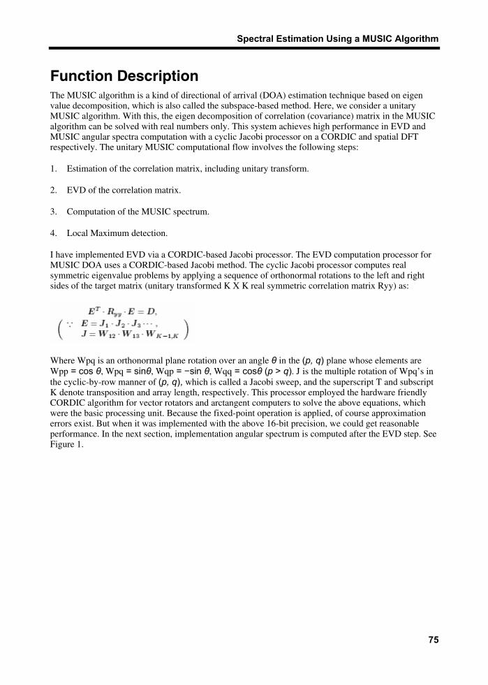
Function Description The MUSIC algorithm is a kind of directional of arrival (DOA) estimation technique based on eigen value decomposition, which is also called the subspace-based method. Here, we consider a unitary MUSIC algorithm. With this, the eigen decomposition of correlation (covariance) matrix in the MUSIC algorithm can be solved with real numbers only. This system achieves high performance in EVD and MUSIC angular spectra computation with a cyclic Jacobi processor on a CORDIC and spatial DFT respectively. The unitary MUSIC computational flow involves the following steps:
1. Estimation of the correlation matrix, including unitary transform.
2. EVD of the correlation matrix.
3. Computation of the MUSIC spectrum.
4. Local Maximum detection.
I have implemented EVD via a CORDIC-based Jacobi processor. The EVD computation processor for MUSIC DOA uses a CORDIC-based Jacobi method. The cyclic Jacobi processor computes real symmetric eigenvalue problems by applying a sequence of orthonormal rotations to the left and right sides of the target matrix (unitary transformed K X K real symmetric correlation matrix Ryy) as:
Where Wpq is an orthonormal plane rotation over an angle θ in the (p, q) plane whose elements are Wpp = cos θ, Wpq = sinθ, Wqp = −sin θ, Wqq = cosθ (p > q). J is the multiple rotation of Wpq’s in the cyclic-by-row manner of (p, q), which is called a Jacobi sweep, and the superscript T and subscript K denote transposition and array length, respectively. This processor employed the hardware friendly CORDIC algorithm for vector rotators and arctangent computers to solve the above equations, which were the basic processing unit. Because the fixed-point operation is applied, of course approximation errors exist. But when it was implemented with the above 16-bit precision, we could get reasonable performance. In the next section, implementation angular spectrum is computed after the EVD step. See Figure 1.
Nios II Embedded Processor Design Contest—Outstanding Designs 2005
76
Figure 1. System Overview
]Re[ 11HXX •
]Re[ 22HXX •
]Re[ HMM XX •
... ...
...
Performance Parameters The estimated performance of the dominant core functions is the number of occupied logic blocks in the FPGA and fMAX is the maximum clock frequency at which normal operation can be guaranteed. The minimum computation time, tmin, is calculated by required clks * fMAX. I assumed that less than 2 coherent/incoherent waves arrived at only 4-element uniform linear array antenna. For spectrum generation, 256-point radix-4 complex fast Fourier transform (FFT) was employed and the FFT with 256 spatial data composed of N elements of the noise eigenvector and (256−N) zeroes interpolates the spectrum fine and smoothly. All computations were performed by fixed-point arithmetic with 12-bit input data from ADCs. On the other hand, the estimation accuracy of the EVD system depends on so many factors that the proper assessment has some difficulties in detailed analysis. For example, the effect of finite bit-length and bit-truncation by scaling in the fixed-point operation, the estimation errors caused by non-uniform discrete wavefront, and so forth.
Design Architecture The EVD of the input matrix X can be performed, as illustrated in Figure 2, using the well known systolic array architecture. The rows of matrix X are fed as inputs to the array from the top, along with the corresponding element of the vector y. The R and u values, held in each of the cells once all the inputs have been passed through the matrix, are the outputs from the EVD. These values are subsequently used to derive the coefficients using a back substitution technique.

Spectral Estimation Using a MUSIC Algorithm
77
Figure 2. EVD of the Input Matrix
The CORDIC rotation-based algorithm is implemented in a very efficient pipelined manner using a triangular systolic array. The schematic is shown in Figure 3, for M = 4 antenna elements.
Figure 3. CORDIC Rotation-Based Algorithm Schematic
Vec. Rot.
x1(t) x2(t - 1)
Rot.
x3(t - 2)
Rot.
y(t - 3)
A B D
Rot. Vec. Rot. Rot.
D0 1F
Rot. Vec. Rot.E
0
C
Rot
G
0
H
CPE
xi
n
yi
n
�out
(�out)
xout yout
�in
(�in)
e(t - 7)
Φ - CPE
Θ - CPE1 Θ - CPE2
(|xin|)Im(r)Re(r)
Re(xout) Im(xout)
σΦ,out
σΦ,outσΦ,in
σΦ,in
Re(xin) Im(xin)
(a) (b)
The cells in the triangular array (A-B-C) store the elements of the evolving triangular matrix R[i], and the ones in the right hand column (D-E) store the elements of the updated vector u[i]. The data flow is from top to bottom, while the rotation angles are propagated from left to the right of the array. In this implementation, the array entirely consists of CORDIC processor elements (CPEs), which work completely synchronously, driven by a single global master clock. Because all the CPEs need the same amount of time to perform their computations they never get flooded with data. Thereby, the CPEs designated with Vec are configured to the “vectoring” mode of operation, and those labeled with Rot operate in the “rotation” mode. Each row performs a given rotation, whereby the rotation angle is determined by the CPE in vectoring mode at the beginning of the row. The rotation angle is passed to the rotation CPEs to the right with one clock cycle delay, thus requiring the elements of the data vector to be applied to the array in a time-staggered fashion, as indicated by the indices in Figure 3. To handle the complex data, complex CORDIC is used. As shown above, it is comprised of three CPEs interconnected according to figure 4b. In vectoring mode (Im(rm,m) = 0), the imaginary part of the complex value xm is annihilated by the Φ-CPE and subsequently | xm| is zeroed in θ-CPE1. The complex Givens rotation is then coded by the two sequences of rotation coefficients {σΦ,j} and {σθ,j}. By applying these rotation coefficients to a supercell configured to operate in the rotation mode, the incoming vector (Re(xin) Im(yin))
T is rotated by Φm in the Φ-CPE and subsequently the real and imaginary parts of rm,n and xm,n are each rotated by θm in θ-CPE1 and θ-CPE2, respectively.
Nios II Embedded Processor Design Contest—Outstanding Designs 2005
78
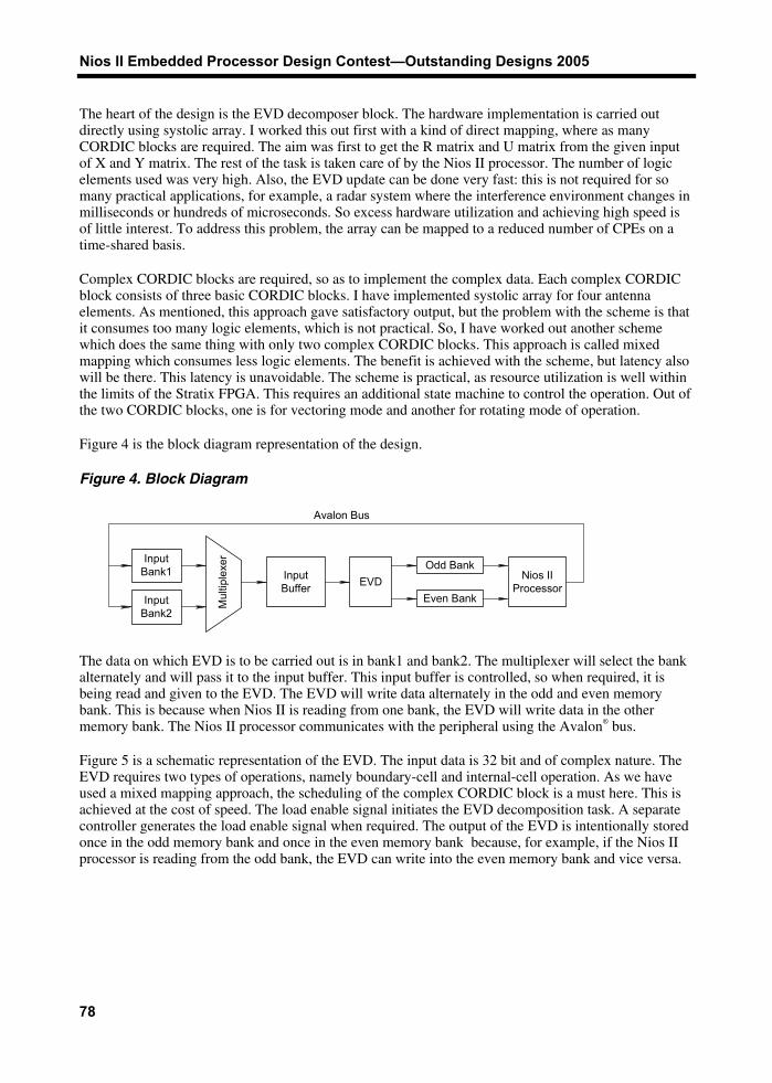
The heart of the design is the EVD decomposer block. The hardware implementation is carried out directly using systolic array. I worked this out first with a kind of direct mapping, where as many CORDIC blocks are required. The aim was first to get the R matrix and U matrix from the given input of X and Y matrix. The rest of the task is taken care of by the Nios II processor. The number of logic elements used was very high. Also, the EVD update can be done very fast: this is not required for so many practical applications, for example, a radar system where the interference environment changes in milliseconds or hundreds of microseconds. So excess hardware utilization and achieving high speed is of little interest. To address this problem, the array can be mapped to a reduced number of CPEs on a time-shared basis.
Complex CORDIC blocks are required, so as to implement the complex data. Each complex CORDIC block consists of three basic CORDIC blocks. I have implemented systolic array for four antenna elements. As mentioned, this approach gave satisfactory output, but the problem with the scheme is that it consumes too many logic elements, which is not practical. So, I have worked out another scheme which does the same thing with only two complex CORDIC blocks. This approach is called mixed mapping which consumes less logic elements. The benefit is achieved with the scheme, but latency also will be there. This latency is unavoidable. The scheme is practical, as resource utilization is well within the limits of the Stratix FPGA. This requires an additional state machine to control the operation. Out of the two CORDIC blocks, one is for vectoring mode and another for rotating mode of operation.
Figure 4 is the block diagram representation of the design.
Figure 4. Block Diagram
Mul
tiple
xerInput
Bank1
InputBank2
EVDOdd Bank
Even Bank
Nios IIProcessor
Input Buffer
Avalon Bus
The data on which EVD is to be carried out is in bank1 and bank2. The multiplexer will select the bank alternately and will pass it to the input buffer. This input buffer is controlled, so when required, it is being read and given to the EVD. The EVD will write data alternately in the odd and even memory bank. This is because when Nios II is reading from one bank, the EVD will write data in the other memory bank. The Nios II processor communicates with the peripheral using the Avalon® bus.
Figure 5 is a schematic representation of the EVD. The input data is 32 bit and of complex nature. The EVD requires two types of operations, namely boundary-cell and internal-cell operation. As we have used a mixed mapping approach, the scheduling of the complex CORDIC block is a must here. This is achieved at the cost of speed. The load enable signal initiates the EVD decomposition task. A separate controller generates the load enable signal when required. The output of the EVD is intentionally stored once in the odd memory bank and once in the even memory bank because, for example, if the Nios II processor is reading from the odd bank, the EVD can write into the even memory bank and vice versa.
Spectral Estimation Using a MUSIC Algorithm
79
Figure 5. EVD Schematic Representation
EVD
clk
reset
32-Bit Data
load-en
32-Bit Odd Memory
32-Bit Even Memory
Figure 6 is a simplified view of the controller responsible for generating control signals, as necessary.
Figure 6. Controller
Controller
clk
reset
done_reset
cordic_clk
load_enable
data_sel_pass1
bank_sel
vec_rot_sel_pass1
rd_wr_x
vec_rot_sel_pass1
global_ress
done
cordic_clock_by2
read_address_out[5:0]
The register transfer level (RTL) view of the controller is shown in Figure 7.
It is a finite state machine that uses a counter and mealy state machine. It generates the following control signals for different blocks. It is the central unit for the EVD processor. When the load_en signal comes, as long as high loading of the data takes place, as soon as load_en goes low, the controller acts. It generates:
1. bank select signal for switching the y memory bank data and address.
2. vec_rot_sel signal, which is used to multiplex between the vector and rotation modes of the complex CORDIC.
3. address signal for writing into the memory and reading from the memory.
4. Done signal, which goes high when the EVD operation is over.

Nios II Embedded Processor Design Contest—Outstanding Designs 2005
80
Figure 7. RTL View of Controller
row_end_gen_9
data_read_gen1_tc
bank_sel_cnt
bank_sel_tc_gen1
reg_genZ3
input_data_read_sel
reset_gen_counter
tc_bank_en_gen
reg_gen_enZ2
tc_9_reg1
row_end_gen
read_address_gen1_lsb
row_end_gen
read_address_gen1_msb
reg_genZ3
bank_sel_gen1
reg_gen_enZ2
neg_edge_bank_sel
reg_genZ3
load_en_reg_rdwr
timing_cnt
rd_wr_gen1
reg_genZ3
reg_rdwr1
reg_genZ3
reg_rdwr2
timing_cnt
cordic_clk_by2_1
done_counter
done_inst
reg_genZ3
reg_done1
reg_genZ3
reg_done2
global_reset_out
cordic_clk_by2
global_reset_rdwr
un1_bank_end_tc_mod
rd_wr_x_sig
bank_end_tc_modclk_en
cordic_clk_by2
global_reset_out
rd_wr_x
vec_rot_sel_pass2
read_address_out[5:0]
load_en
cordic_clock
reset
[2:0]
resetclk
1clk_en
row_end
[3:0]address[3:0]
reset
clk1
clk_enrow_end
[3:0]
address[3:0]
reset
clk
ri[0]ro[0]
reset
clk
1clk_en
vec_rot_sel_pass1
vec_rot_sel_pass2
bank_end
address[4:0]
resetclk
1 clk_en
ri[0]ro[0]
resetclk
1clk_en
row_end
[3:0]address[3:0]
reset
clk1
clk_en
row_end
[3:0]address[3:0]
resetclkri[0]
ro[0]
resetclkclk_enri[0]
ro[0]
reset
clk
ri[0]
ro[0]reset
clk
start
[3:0]address[3:0]
resetclk
ri[0]ro[0]
reset
clk
ri[0]
ro[0]
reset
clk
start
output_en
[3:0]address[3:0]
resetclk
1clk_en
tc
address[7:0]
resetclkri[0]
ro[0]
resetclkri[0]
ro[0]
[2]
[3]
done
row_end_10
bank_sel1
output_en
clk
done_reset
data_sel_pass1
bank_end_tc_out
vec_rot_sel_pass1
[2:0]
bank_end_rdwr_dis
Figure 8 shows the complex CORDIC block and the equivalent RTL is shown in Figure 9.
Figure 8. Complex CORDIC
Complex CORDIC
clk
reset
start
output_en
r_x_real_in[21:0]
r_x_imag_in[21:0]
xin_real[21:0]
xin_imag[21:0]
vec_rot_sel
xout_real_th[21:0]
xout_real_th_next[21:0]
xout_imag_th[21:0]
xout_imag_th_next[21:0]

Spectral Estimation Using a MUSIC Algorithm
81
Figure 9. RTL of Complex CORDIC
vec_rot
vec_rot_inst
reg_gen_enZ2
vec_rot_sel_delay1
reg_gen_enZ2
output_delay
reg_gen_enZ1
phi_store
mux_genZ3
mux_vec
reg_gen_enZ2
vec_rot_sel_reg1
reg_gen_enZ2
vec_rot_sel_delay2
vec_rot
vec_rot_theta_real
reg_gen_enZ1
theta_real_store
vec_rot
vec_rot_theta_imag
reg_gen_enZ1
theta_imag_store
xout_imag_th_next[21:0][21:0]
[21:0]
xout_imag_th[21:0][21:0]
xout_real_th[21:0][21:0]
R_x_imag_in[21:0][21:0]
R_x_real_in[21:0][21:0]
xin_imag[21:0][21:0]
xin_real[21:0]
[21:0]
vec_rot_sel
output_en
start
reset
clk
clk
reset
start1 clk_en
output_en
vec_rot_sel[21:0]
dataa[21:0][21:0]
datab[21:0][17:0]
zin[17:0]
[21:0]x_out[21:0]
[21:0]y_out[21:0]
result[17:0]
reset
clk1
clk_en
ri[0]
ro[0]
reset
clk1
clk_en
ri[0]
ro[0]
reset
clk
clk_en[17:0]
ri[17:0]
[17:0]ro[17:0]
sel
[21:0]A[21:0]
[21:0]B[21:0]
[21:0]
mux_out[21:0]
reset
clk1
clk_en
ri[0]
ro[0]
reset
clk1 clk_en
ri[0]
ro[0]
clk
reset
start1 clk_en
output_en
vec_rot_sel[21:0]
dataa[21:0]
datab[21:0]
zin[17:0]
[21:0]x_out[21:0]
[21:0]y_out[21:0]
[17:0]result[17:0]
reset
clkclk_en
[17:0]ri[17:0]
[17:0]ro[17:0]
clk
reset
start1
clk_en
output_en
vec_rot_sel[21:0]
dataa[21:0][21:0]
datab[21:0]
[17:0]zin[17:0]
[21:0]x_out[21:0]
[21:0]
y_out[21:0]
[17:0]result[17:0]
reset
clk
clk_en[17:0]
ri[17:0]
[17:0]ro[17:0]
[21:0]
[17:0]
This complex CORDIC block is the key block for EVD. It comprises three CORDIC blocks and one phi-CORDIC block. These blocks are used for compensating the imaginary part of the complex input, the two theta-CORDIC ones are for the real part and the other is for the imaginary part. Because we are using a complex CORDIC in a time division multiplex manner, the angles phi and theta are stored in vector mode and these angles are used subsequently in rotation mode. The output block is important, as shown in Figure 10, for storing the final result and generating the control-signal-like interrupt when EVD is over. It also provides all necessary addresses and bus control signals for interfacing with the Nios II processor.
Figure 10. Output Block
address_wr_op
address_read_inst
reg_gen_enZ4
tc_reg_1
address_wr_op
address_wirte_inst
mux_genZ2
mux_rd_wr_address_instload_en
cordic_clock
address_rd_wr[5:0][5:0]
address_rd[5:0][5:0]
rd_wr
done
reset
reset
clk
1clk_en
tc
[5:0]address[5:0]
reset
clk
1clk_en
ri[0]
ro[0] reset
clk
1clk_en
tc
address[5:0]
sel
[5:0]A[5:0]
B[5:0]
mux_out[5:0]
[5:0]
[5:0] [5:0
]
clk

Nios II Embedded Processor Design Contest—Outstanding Designs 2005
82
CORDIC Architecture I have implemented CORDIC as an iterative architecture that is a direct translation from CORDIC equations.
The CORDIC rotator is normally operated in one of two modes. The first mode, called rotation mode, rotates the input vector specified angle. The second mode, called vectoring, rotates the input vector to the x-axis while recording the angle required to make that rotation.
Rotation Mode
In rotation mode, the angle accumulator is initialized with the desired rotation angle. The rotation decision at each iteration is made to diminish the magnitude of the residual angle accumulator. The decision at each iteration is therefore based on the sign of the residual angle after each step.
Vectoring Mode
In vectoring mode, the CORDIC rotator rotates the input vector through whatever angle is necessary to align the result vector with the x axis. The result of the vectoring operation is a rotation angle and the scaled magnitude of the original vector (x component of the result). The vectoring function works by seeking to minimize the y component of the residual vector at each rotation. The sign of the residual y component is used to determine which direction to rotate next.
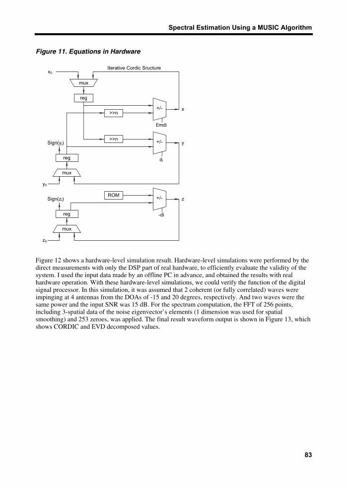
An iterative CORDIC architecture can be obtained by duplicating each of the three difference equations in hardware as shown in Figure 11. The decision function, di, is driven by the sign of the y or z register, depending on whether it is operating in the rotation or vectoring mode. In operation, the initial values are loaded via multiplexers into the x, y and z registers. Then on each of the next n clock cycles, the values from the registers are passed through the shifters and adder-subtractors and the result is placed back in the registers. At each iteration, the shifters are modified to cause the desired shift for the operation. Likewise, at each iteration, the ROM address is incremented so that the appropriate elementary angle value is presented to the z adder-subtractor. On the last iteration, the results are read directly from the adder-subtractors.
Spectral Estimation Using a MUSIC Algorithm
83
Figure 11. Equations in Hardware
mux
reg
>>n+/-
£mdi
x
+/-
di
y>>n
reg
Sign(yi)
mux
y0
+/-
-di
zROM
reg
Sign(zi)
mux
z0
x0Iterative Cordic Sructure
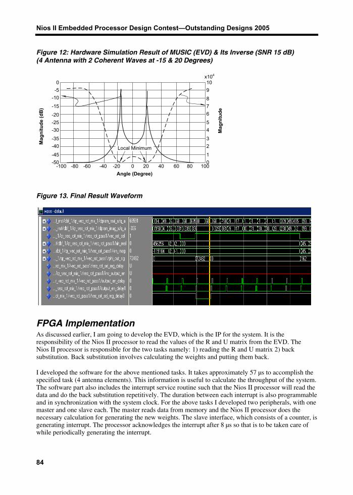
Figure 12 shows a hardware-level simulation result. Hardware-level simulations were performed by the direct measurements with only the DSP part of real hardware, to efficiently evaluate the validity of the system. I used the input data made by an offline PC in advance, and obtained the results with real hardware operation. With these hardware-level simulations, we could verify the function of the digital signal processor. In this simulation, it was assumed that 2 coherent (or fully correlated) waves were impinging at 4 antennas from the DOAs of -15 and 20 degrees, respectively. And two waves were the same power and the input SNR was 15 dB. For the spectrum computation, the FFT of 256 points, including 3-spatial data of the noise eigenvector’s elements (1 dimension was used for spatial smoothing) and 253 zeroes, was applied. The final result waveform output is shown in Figure 13, which shows CORDIC and EVD decomposed values.
Nios II Embedded Processor Design Contest—Outstanding Designs 2005
84
Figure 12: Hardware Simulation Result of MUSIC (EVD) & Its Inverse (SNR 15 dB) (4 Antenna with 2 Coherent Waves at -15 & 20 Degrees)
0-5
-10
-15
-20-25-30
-35-40
-45-50
-100 -80 -60 -40 -20 0 20 40 60 80 10001
23
45
678
910
x104
Mag
nitu
de
Local Minimum
Angle (Degree)
Mag
nitu
de (d
B)
Figure 13. Final Result Waveform
FPGA Implementation As discussed earlier, I am going to develop the EVD, which is the IP for the system. It is the responsibility of the Nios II processor to read the values of the R and U matrix from the EVD. The Nios II processor is responsible for the two tasks namely: 1) reading the R and U matrix 2) back substitution. Back substitution involves calculating the weights and putting them back.
I developed the software for the above mentioned tasks. It takes approximately 57 µs to accomplish the specified task (4 antenna elements). This information is useful to calculate the throughput of the system. The software part also includes the interrupt service routine such that the Nios II processor will read the data and do the back substitution repetitively. The duration between each interrupt is also programmable and in synchronization with the system clock. For the above tasks I developed two peripherals, with one master and one slave each. The master reads data from memory and the Nios II processor does the necessary calculation for generating the new weights. The slave interface, which consists of a counter, is generating interrupt. The processor acknowledges the interrupt after 8 µs so that is to be taken care of while periodically generating the interrupt.
Spectral Estimation Using a MUSIC Algorithm
85
The hardware-software co-simulation in the ModelSim® tool helped me to resolve the problem, and to estimate the time taken by the processor to acknowledge the interrupt. The program developed for the back substitution is not fixed for four antenna elements, but it is a general program, applicable to any number of antenna elements.
The Avalon bus is a simple bus architecture designed for connecting on-chip processors and peripherals together into a system-on-a-programmable-chip (SOPC) solution. See Figure 14. It is an interface that specifies the port connections between master and slave components. Basic Avalon bus transactions transfer a single byte, half word, or word between a master and slave peripheral. After the completion of a transfer, the bus is available on the next clock cycle for any another transaction.
Figure 14. Avalon Bus
Data &ProgramMemory
R_r R_i U_r U_i
Mixed Mode EVD_Decomposer
Avalon Bus
Nios II Processor C_r C_i
Some key features of the Avalon bus are:
■ Memory and peripherals may be mapped anywhere within the 32- bit address space.
■ All Avalon signals are synchronized to the Avalon bus clock, which simplifies the timing behavior of the Avalon bus and facilitates integration with high-speed peripherals.
■ Separate, dedicated address and data paths provide the easy interface to on chip user logic. Peripherals do not need to decode data and address bus cycles.
■ The Avalon bus automatically generates chip select signals for all peripherals, greatly simplifying the design of Avalon peripherals.
■ Multiple master peripherals can reside on the Avalon bus. The Avalon bus generates the required arbitration logic.
■ The Avalon bus also handles the details of transferring data between peripherals with mismatched data widths.
Device Utilization Summary Family Stratix Device EP1S10F780C6ES Total logic elements 8,236 / 10,570 ( 77 % ) Total pins 34 / 427 ( 31 % ) Total memory bits 61,856 / 920,448 ( 6 % ) DSP block 9-bit elements 8 / 48 ( 16 % ) Total phase-locked loops (PLLs) 1 / 6 ( 16 % ) Total DLLs 0 / 2 ( 0 % )

Nios II Embedded Processor Design Contest—Outstanding Designs 2005
86
Test Results & Comparison I have undergone a full design cycle of an SOPC implementation, i.e., hardware-software co-design, integration of peripherals with Avalon bus, etc. A hardware-based approach is accelerating the performance. The new hardware-based computing will solve the bottleneck of algorithmic signal processing. It is discovered that, if a CORDIC block is implemented in software only, it takes 8,600 clock cycles to complete the vectoring mode of operation as opposed to what I have achieved: 16 clock cycles to accomplish the same task in hardware. This result can motivate a CORDIC-based EVD. With respect to accuracy, if we compare the Arctan function implementation in software only, it requires approximately 20,000 clock cycles to achieve the same accuracy as the Arctan IP developed with a hardware approach. We achieved the desired functionality with the Nios II processor running at a clock speed of 50 MHz on a Stratix board. Our design of the EVD IP only takes 55 percent of the chip area on the Stratix FPGA.
Performance Comparison Software Approach
Method
CORDIC (Cycles)
CORDIC EVD (Cycles)
Direct Equation
8,600 (172 us) 90,3000 (18 us)
Arctan Series Expansion
20,000 (400 us) 2,100,000 (42 ms)
Hardware Approach
CORDIC (Cycles) CORDIC EVD (Cycles)
16
16 (EVD update latency will be 16 cycles) = 320 ns
Logic Elements Utilization for EVD Decomposer
Method Logic Elements
Direct Mapping 34,055 Mapping Each Row 7,811 Mixed Mapping 4,946
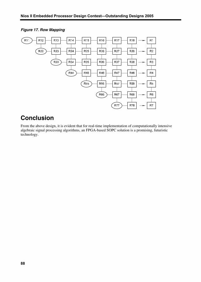
Design Features I tried different mapping architectures for optimum implementation. This section shows different mapping for seven antenna elements. Figure 15 shows direct mapping.

Spectral Estimation Using a MUSIC Algorithm
87
Figure 15. Direct Mapping
Figure 16 shows mix mapping and Figure 17 shows row mapping. Round blocks indicate the vectoring mode of operation. Square blocks indicate the rotating mode of operation.
Figure 16. Mix Mapping
Nios II Embedded Processor Design Contest—Outstanding Designs 2005
88
Figure 17. Row Mapping
Conclusion From the above design, it is evident that for real-time implementation of computationally intensive algebraic signal processing algorithms, an FPGA-based SOPC solution is a promising, futuristic technology.

Altera, The Programmable Solutions Company, the stylized Altera logo, specific device designations, and all other words and logos that are identified as trademarks and/or service marks are, unless noted otherwise, the trademarks and service marks of Altera Corporation in the U.S. and other countries. All other product or service names are the property of their respective holders. Altera products are protected under numerous U.S. and foreign patents and pending applications, mask work rights, and copyrights.