Embed Size (px)
Citation preview

University of Technology, Sydney
Spectroscopic Studies of
Hydrogen Dopants in
ZnO Crystals
by
Laurent Olivier Lee Cheong Lem
A thesis submitted in partial fulfillment for
the degree of Doctor of Philosophy
in the
School of Physics and Advanced Materials
Faculty of Science
2013

Declaration of Authorship
I, Laurent Olivier Lee Cheong Lem, declare that this thesis titled, ‘Spectro-
scopic Studies of Hydrogen Dopants in ZnO Crystals’ and the work presented in
it are my own. I confirm that:
� This work was done wholly or mainly while in candidature for a research
degree at this University.
� Where any part of this thesis has previously been submitted for a degree or
any other qualification at this University or any other institution, this has
been clearly stated.
� Where I have consulted the published work of others, this is always clearly
attributed.
� Where I have quoted from the work of others, the source is always given.
With the exception of such quotations, this thesis is entirely my own work.
� I have acknowledged all main sources of help.
� Where the thesis is based on work done by myself jointly with others, I have
made clear exactly what was done by others and what I have contributed
myself.
Signed:
Date:
i

Abstract
ZnO is a semiconductor with a direct band gap of 3.37 eV and an exciton binding
energy of 60meV at room temperature. These properties make it an attractive
material for optoelectronic devices across a wide range of applications. Significant
obstacles preventing the wide scale usage of ZnO include the lack of reliable p-
type doping and high uncertainty surrounding the nature of its defects. Moreover,
as-grown ZnO is intrinsically n-type and it is thought that hydrogen is the cause
for the high n-type character.
The aim of this thesis is therefore to elucidate the role of hydrogen with respect to
the optical and electrical properties of ZnO as well as its interaction with native
defects and impurities.
During this work, hydrogen was introduced in ZnO single crystals through an
RF plasma source. Hydrogen incorporation was confirmed by XPS measurements
which showed an increase in hydrogenated oxygen states. Hydrogen also modified
the near-surface region of the crystals only and not the bulk.
Hydrogen doped ZnO showed significant increases in the carrier concentration
as well as in the near band edge (NBE) luminescence. This is attributed to hy-
drogen introducing new shallow donors. The green luminescence, whose origin
is attributed to VZn, was quenched after hydrogen incorporation, indicating for-
mation of neutral VZn-H2 complexes. The yellow luminescence in the as-received
crystal is identical to that in Li doped ZnO and was assigned to recombinations
involving LiZn.
Hydrogen doped ZnO also exhibits a negative thermal quenching (NTQ) of the
NBE luminescence where the intensity of the luminescence increases with increas-
ing temperature. Q-DLTS measurements detected new electronic states being
created following hydrogen incorporation. A model involving the H-related state

iii
at 11meV releasing electrons to form free excitons is proposed to explain the
NTQ behaviour.
XANES studies of H-doped ZnO showed that hydrogen interacted with oxygen
states only but not zinc. This suggests that most of the hydrogen dopants intro-
duced by plasma sit at the oxygen anti-bonding site.
The recombination kinetics of the various luminescence was investigated. While
the kinetics of the NBE luminescence followed the expected behaviour for exci-
tonic type recombination, the green and yellow luminescences showed high tem-
perature dependencies and is explained in terms of different recombination mech-
anisms.
Finally, it was found that hydrogen is stable under normal SEM excitation con-
ditions.

Acknowledgements
I would like to thank my supervisors Dr. Cuong Ton-That and Prof. Matthew
Phillips for allowing me to work in their research group and for all their support,
guidance and help they have offered me during my time as a student at the
University of Technology, Sydney.
I would also like to extend my gratitude to Geoff McCredie for his help with
the plasma chamber and also the staff of the MAU for their help with sample
preparation and data collection, acquisition and analysis.
To Mark Lockrey and Trevor Manning for their help with using and developing
the CL system.
To Christian Nenstiel for his help with the PL measurements.
To my fellow research students and colleagues in the MAU for their insightful
discussions and ideas and for contributing to a cheerful and pleasant atmosphere.
You have made my time at UTS not only successful, but enjoyable.
To my family and friends for their understanding and support during this daunt-
ing and important endeavour.
iv

Contents
Declaration of Authorship i
Abstract ii
Acknowledgements iv
List of Publications viii
List of Figures ix
List of Tables xii
List of Acronyms xiii
1 Introduction to Zinc Oxide 1
1.1 Zinc Oxide as an Optoelectronic Material . . . . . . . . . . . . . . 1
1.2 Motivation of the Research . . . . . . . . . . . . . . . . . . . . . . 3
1.3 Aim and Objectives of This Dissertation . . . . . . . . . . . . . . 4
1.4 Thesis Structure . . . . . . . . . . . . . . . . . . . . . . . . . . . . 5
2 Defects and Hydrogen Impurities in ZnO: A Review of CurrentStatus 6
2.1 Physical Properties . . . . . . . . . . . . . . . . . . . . . . . . . . 6
2.2 Crystal Structure . . . . . . . . . . . . . . . . . . . . . . . . . . . 6
2.3 Band Structure of ZnO . . . . . . . . . . . . . . . . . . . . . . . . 8
2.4 Crystallographic defects . . . . . . . . . . . . . . . . . . . . . . . 10
2.4.1 Vacancies . . . . . . . . . . . . . . . . . . . . . . . . . . . 11
2.4.2 Interstitials . . . . . . . . . . . . . . . . . . . . . . . . . . 14
2.4.3 Antisites . . . . . . . . . . . . . . . . . . . . . . . . . . . . 14
2.4.4 Impurities . . . . . . . . . . . . . . . . . . . . . . . . . . . 15
2.4.5 Formation Energies of Native Defects . . . . . . . . . . . . 15
v

Contents vi
2.5 Optical Processes in ZnO . . . . . . . . . . . . . . . . . . . . . . . 17
2.5.1 Exciton Formation . . . . . . . . . . . . . . . . . . . . . . 18
2.5.2 Recombination of electron-hole pairs . . . . . . . . . . . . 20
2.5.3 Radiative Recombination . . . . . . . . . . . . . . . . . . . 20
2.5.3.1 Near Band Edge Emission . . . . . . . . . . . . . 20
2.5.3.2 Deep Level Emission . . . . . . . . . . . . . . . . 22
2.5.3.3 Green Luminescence . . . . . . . . . . . . . . . . 23
2.5.3.4 Yellow Luminescence . . . . . . . . . . . . . . . . 24
2.5.3.5 Red Luminescence . . . . . . . . . . . . . . . . . 25
2.5.3.6 Summary . . . . . . . . . . . . . . . . . . . . . . 25
2.5.4 Non-Radiative Recombination . . . . . . . . . . . . . . . . 26
2.5.4.1 Non-Radiative via Deep Level . . . . . . . . . . . 26
2.5.4.2 Auger Recombination . . . . . . . . . . . . . . . 26
2.5.4.3 Surface Recombination . . . . . . . . . . . . . . . 27
2.6 Hydrogen in ZnO . . . . . . . . . . . . . . . . . . . . . . . . . . . 27
2.6.1 Hydrogen as a Donor . . . . . . . . . . . . . . . . . . . . . 28
2.6.2 Location of Hydrogen in the Lattice . . . . . . . . . . . . . 30
2.6.3 Interaction of Hydrogen With Defects . . . . . . . . . . . . 31
3 Experimental Details 33
3.1 ZnO Crystal Specimen . . . . . . . . . . . . . . . . . . . . . . . . 33
3.2 Sample Cleaning and Preparation . . . . . . . . . . . . . . . . . . 35
3.3 Hydrogen Doping . . . . . . . . . . . . . . . . . . . . . . . . . . . 35
3.4 Scanning Electron Microscopy (SEM) . . . . . . . . . . . . . . . . 36
3.5 Cathodoluminescence Spectroscopy . . . . . . . . . . . . . . . . . 38
3.5.1 CL System Calibration . . . . . . . . . . . . . . . . . . . . 40
3.6 Monte Carlo Simulations (CASINO) . . . . . . . . . . . . . . . . 42
3.7 Electrical Measurements . . . . . . . . . . . . . . . . . . . . . . . 45
3.7.1 Resistivity Measurement . . . . . . . . . . . . . . . . . . . 45
3.7.2 Hall Measurement . . . . . . . . . . . . . . . . . . . . . . . 46
3.8 Synchrotron Light Experiments . . . . . . . . . . . . . . . . . . . 47
3.8.1 X-Ray Photoelectron Spectroscopy . . . . . . . . . . . . . 47
3.8.2 X-Ray Absorption Near Edge Spectroscopy . . . . . . . . . 49
3.9 Raman Spectroscopy . . . . . . . . . . . . . . . . . . . . . . . . . 50
3.10 Charge-based Deep Level Transient Spectroscopy . . . . . . . . . 52
3.11 Other Characterisation Techniques . . . . . . . . . . . . . . . . . 54
4 Hydrogen Doped ZnO 55
4.1 Introduction . . . . . . . . . . . . . . . . . . . . . . . . . . . . . . 55
4.2 Crystal Morphology and Structure . . . . . . . . . . . . . . . . . 56
4.3 Electrical Properties of Hydrogen Doped ZnO . . . . . . . . . . . 59
4.4 Optical Properties of Hydrogen doped ZnO . . . . . . . . . . . . . 60
Contents vii
4.4.1 Effects of Hydrogen on the NBE luminescence . . . . . . . 62
4.4.2 Effects of Hydrogen on the DLE . . . . . . . . . . . . . . . 65
4.4.3 Effects of Temperature on Hydrogen Incorporation . . . . 66
4.4.4 Deconvolution of the Deep-Level Luminescence Band . . . 69
4.4.5 Depth Distribution of Luminescence Centres . . . . . . . . 72
4.4.5.1 Simulations of CL Interaction Volumes in ZnO . 73
4.4.5.2 Distribution of Luminescence Centres in H-dopedZnO . . . . . . . . . . . . . . . . . . . . . . . . . 75
4.4.6 Effect of Plasma Exposure Time on the Luminescence . . . 78
4.5 Raman Spectroscopy . . . . . . . . . . . . . . . . . . . . . . . . . 81
4.6 Synchrotron Light Measurements . . . . . . . . . . . . . . . . . . 85
4.6.1 X-Ray Photoelectron Spectroscopy . . . . . . . . . . . . . 85
4.6.2 X-Ray Absorption Near Edge Spectroscopy . . . . . . . . . 92
4.7 Summary . . . . . . . . . . . . . . . . . . . . . . . . . . . . . . . 101
5 Hydrogen States and Recombination Kinetics in ZnO 103
5.1 Introduction . . . . . . . . . . . . . . . . . . . . . . . . . . . . . . 103
5.2 Temperature Dependence of the Luminescence . . . . . . . . . . . 104
5.3 Negative Thermal Quenching of the NBE Luminescence . . . . . . 112
5.4 Shallow Carrier Traps in ZnO . . . . . . . . . . . . . . . . . . . . 117
5.5 Recombination Kinetics . . . . . . . . . . . . . . . . . . . . . . . 123
5.6 Characteristics of the Yellow Luminescence . . . . . . . . . . . . . 130
5.7 Stability of Hydrogen Under the Electron Beam in ZnO . . . . . . 132
5.8 Summary . . . . . . . . . . . . . . . . . . . . . . . . . . . . . . . 140
6 Conclusions and Future Directions 142
6.1 Conclusions . . . . . . . . . . . . . . . . . . . . . . . . . . . . . . 142
6.2 Future Directions . . . . . . . . . . . . . . . . . . . . . . . . . . . 145
6.3 Closing Remarks . . . . . . . . . . . . . . . . . . . . . . . . . . . 146
Bibliography 147

List of Publications
Refereed Journal Publications
Lee Cheong Lem, L., Ton-That, C., and Phillps, M.R. Distribution of visibleluminescence centers in hydrogen-doped ZnO, Journal of Material Research,26(23):2912, 2011.
Oral Presentations
Lee Cheong Lem, L., Ton-That, C., and Phillps, M.R. Investigations ofhydrogen dopants in H-doped ZnO.Australian Microbeam Analysis Society XII, Sydney. February 2013.
Lee Cheong Lem, L., Ton-That, C., and Phillps, M.R. Temperaturedependence of cathodoluminescence of hydrogen doped zinc oxide.ACCM 22 / APMC 10 / ICONN 2012, Perth, February 2012.
Lee Cheong Lem, L., Ton-That, C., and Phillps, M.R. Distributionof green and yellow luminescence centres in H-doped ZnO.Australian Microbeam Analysis Society XI, Canberra. February 2011.
viii
List of Figures
2.1 Unit cells for common ZnO structures. . . . . . . . . . . . . . . . 8
2.2 Band structure and splitting of the valence band in ZnO . . . . . 9
2.3 Point defects in ZnO. . . . . . . . . . . . . . . . . . . . . . . . . . 12
2.4 Formation energies of oxygen vacancies . . . . . . . . . . . . . . . 13
2.5 Formation energies of native defects in ZnO. . . . . . . . . . . . . 17
2.6 Typical luminescence spectrum of ZnO . . . . . . . . . . . . . . . 18
2.7 Thermal ionisation of excitons in ZnO and Gan . . . . . . . . . . 19
2.8 Radiative recombination channels . . . . . . . . . . . . . . . . . . 21
2.9 The H+i /H
−i transition level for various semiconductors . . . . . . 28
2.10 Formation energies of interstitial hydrogen in ZnO . . . . . . . . . 29
2.11 Model for Hi in ZnO . . . . . . . . . . . . . . . . . . . . . . . . . 30
3.1 Photograph of ZnO crystal . . . . . . . . . . . . . . . . . . . . . . 34
3.2 Plasma Chamber . . . . . . . . . . . . . . . . . . . . . . . . . . . 36
3.3 Schematic diagram showing key parts of a typical SEM. . . . . . . 37
3.4 Processes induced by electron bombardment. . . . . . . . . . . . . 37
3.5 CL setup . . . . . . . . . . . . . . . . . . . . . . . . . . . . . . . . 39
3.6 CL intensity calibration . . . . . . . . . . . . . . . . . . . . . . . 41
3.7 CL wavelength calibration . . . . . . . . . . . . . . . . . . . . . . 41
3.8 Influence of carrier diffusion on interaction volume . . . . . . . . . 44
3.9 Van der Pauw setup . . . . . . . . . . . . . . . . . . . . . . . . . 45
3.10 X-ray photoionisation cross sections . . . . . . . . . . . . . . . . . 48
3.11 Optical Raman modes in ZnO . . . . . . . . . . . . . . . . . . . . 51
3.12 Q-DLTS band diagram . . . . . . . . . . . . . . . . . . . . . . . . 53
3.13 DLTS setup . . . . . . . . . . . . . . . . . . . . . . . . . . . . . . 53
4.1 X-ray diffraction patterns for ZnO . . . . . . . . . . . . . . . . . . 57
4.2 AFM images of as-received and H-doped ZnO . . . . . . . . . . . 58
4.3 CL spectrum of as-received ZnO . . . . . . . . . . . . . . . . . . . 60
4.4 CL spectrum of as-received ZnO at 10K . . . . . . . . . . . . . . 62
4.5 CL comparison after H-doping . . . . . . . . . . . . . . . . . . . . 63
4.6 PL spectra of as-received and H-doped ZnO . . . . . . . . . . . . 64
4.7 CL on H-doped ZnO performed at different temperatures . . . . . 67
ix

List of Figures x
4.8 Normalised bound exciton emission . . . . . . . . . . . . . . . . . 68
4.9 XPS spectrum of Li doped ZnO . . . . . . . . . . . . . . . . . . . 70
4.10 Lithium doped ZnO spectrum . . . . . . . . . . . . . . . . . . . . 71
4.11 Deconvolution of the DLE peak . . . . . . . . . . . . . . . . . . . 72
4.12 CASINO simulated electron energy loss curves . . . . . . . . . . . 74
4.13 CL generation depth . . . . . . . . . . . . . . . . . . . . . . . . . 74
4.14 Distribution of luminescence centres . . . . . . . . . . . . . . . . . 76
4.15 Time dependent CL . . . . . . . . . . . . . . . . . . . . . . . . . . 79
4.16 Distribution of luminescence centres as a function of plasma time 80
4.17 Raman modes in ZnO . . . . . . . . . . . . . . . . . . . . . . . . 82
4.18 Raman spectra for as-received and H-doped ZnO . . . . . . . . . 84
4.19 XPS survey spectrum of ZnO . . . . . . . . . . . . . . . . . . . . 86
4.20 Inelastic mean free path of electrons . . . . . . . . . . . . . . . . . 89
4.21 O 1s XPS spectrum of ZnO at different X-ray photon energies . . 90
4.22 Valence-band photoemission spectra . . . . . . . . . . . . . . . . . 92
4.23 X-ray attenuation length in ZnO . . . . . . . . . . . . . . . . . . . 93
4.24 XANES experimental geometry . . . . . . . . . . . . . . . . . . . 94
4.25 O K-edge XANES . . . . . . . . . . . . . . . . . . . . . . . . . . . 96
4.26 Zn L-edge XANES for as-received ZnO . . . . . . . . . . . . . . . 99
4.27 Band structure of ZnO . . . . . . . . . . . . . . . . . . . . . . . . 100
5.1 Temperature dependent CL . . . . . . . . . . . . . . . . . . . . . 105
5.2 Energy position of the phonon replica . . . . . . . . . . . . . . . . 107
5.3 Temperature dependent of the FX and phonon replica . . . . . . . 108
5.4 Temperature dependence FX and bound exciton . . . . . . . . . . 110
5.5 Temperature dependence of the NBE peak intensities . . . . . . . 111
5.6 Temperature dependence of the DLE . . . . . . . . . . . . . . . . 112
5.7 NTQ fits to find activation energies . . . . . . . . . . . . . . . . . 115
5.8 I − V characteristics of Au Schottky contacts . . . . . . . . . . . 117
5.9 Q-DLTS spectra of as-received ZnO . . . . . . . . . . . . . . . . . 119
5.10 Q-DLTS spectra of H-doped ZnO . . . . . . . . . . . . . . . . . . 120
5.11 Temperature dependence of the Y line . . . . . . . . . . . . . . . 121
5.12 Mechanism for the NTQ effect . . . . . . . . . . . . . . . . . . . . 122
5.13 DLE emission at low and high beam power . . . . . . . . . . . . . 125
5.14 Power density plots . . . . . . . . . . . . . . . . . . . . . . . . . . 126
5.15 CL spectra at 300K . . . . . . . . . . . . . . . . . . . . . . . . . 128
5.16 Temperature dependence of the FWHM of the YL peak . . . . . . 131
5.17 LEEBI spectra on H-doped ZnO . . . . . . . . . . . . . . . . . . . 133
5.18 Time resolved irradiation on H-doped ZnO . . . . . . . . . . . . . 134
5.19 LEEBI spectra on as-received ZnO . . . . . . . . . . . . . . . . . 136
5.20 Time resolved irradiation on as-received ZnO . . . . . . . . . . . . 137
5.21 Time resolved irradiation of NBE at 10K and 300K . . . . . . . . 138

List of Figures xi
5.22 Time resolved irradiation of DLE at 10K . . . . . . . . . . . . . . 139

List of Tables
1.1 Comparison of different optoelectronic materials . . . . . . . . . . 2
2.1 Compilation of some physical properties of ZnO. . . . . . . . . . . 7
2.2 Summary of bound exciton lines in ZnO at low temperature . . . 22
2.3 Summary of deep level emissions in ZnO . . . . . . . . . . . . . . 25
3.1 ZnO single crystal substrate supplied by MTI Corporation. . . . . 34
3.2 CASINO simulation parameters for depth approximations. . . . . 44
4.1 Hall measurements on as-received and H-doped ZnO . . . . . . . 59
4.2 Fit parameters for yellow and green luminescences . . . . . . . . . 71
4.3 Assignment of XPS peaks . . . . . . . . . . . . . . . . . . . . . . 87
4.4 Summary of XANES peaks . . . . . . . . . . . . . . . . . . . . . . 98
5.1 Varshni fit parameters . . . . . . . . . . . . . . . . . . . . . . . . 109
5.2 Coefficients of the excitation density fits . . . . . . . . . . . . . . 129
xii

List of Acronyms
A0X Neutral acceptor bound excitonAFM Atomic force microscopyASF Atomic sensitivity factor
BX Bound exciton
C-DLTS Capacitance-based deep level transient spectroscopyCB Conduction bandCCD Charge-coupled deviceCVD Chemical vapour depositionCL Cathodoluminescence
D+X Ionised donor bound excitonD0X Neutral donor bound excitonDAP Donor-acceptor pairDFT Density functional theoryDLE Deep level emissionDLTS Deep level transient spectroscopyDRCL Depth-resolved cathodoluminescence
EPR Electron paramagnetic resonance
FTIR Fourier transform infrared spectroscopyFWHM Full width at half maximumFX Free exciton
IMFP Inelastic mean free path
LED Light emitting diodeLO Longitudinal opticalLVM Local vibration mode
NBE Near band edge
xiii

List of Acronyms xiv
PL Photoluminescence
Q-DLTS Charge based deep level transient spectroscopy
sccm standard cubic centimetres per minuteSEM Scanning electron microscopySIMS Secondary ion mass spectrometry
TES Two-electron satellite
UV Ultra-violetUV-Vis Ultra-violet visible
VB Valence band
XANES X-ray absorption near edge spectroscopyXPS X-ray photoelectron spectroscopyXRD X-Ray diffraction

Chapter 1
Introduction to Zinc Oxide
Zinc oxide (ZnO) has been a subject of research for over five decades owing to
its unique properties and possible applications in commercial devices. Its strong
ultraviolet (UV) light absorbing, anti-bacterial and anti-fungal properties have
led to a variety of applications. ZnO powders have been used as pigments in dyes
and paints, or as an active UV absorbing agent in sunscreen to protect against
sunburn and other damage to the skin caused by UV light [1, 2]. It is also being
used as a source of zinc in dietary supplements.
Recently, there has been an increased interest in ZnO being used as a high effi-
ciency optoelectronic material due to its unique physical and optical properties.
Such applications include thin film transistors [3, 4], transparent conducting elec-
trodes and high efficiency light emitting diodes [5, 6] and lasers [7, 8].
1.1 Zinc Oxide as an Optoelectronic Material
ZnO is a direct wide bangap (Eg = 3.37 eV at room temperature) and has a high
exciton binding energy of 60meV. Devices based on ZnO could be more efficient
than ones based on silicon or gallium compounds and would work at elevated
1
Chapter 1. Introduction to ZnO 2
temperatures. These properties, combined with the ability to engineer the band
gap by alloying [9–11], make ZnO an attractive material for the fabrication of
efficient light emitting devices.
ZnO has been studied as a semiconductor for decades now with reported re-
search from Fuller [12] dating from 1929 who reported a way to determine lattice
parameters [13]. Along with germanium and silicon, ZnO was one of the first
semiconductors to be grown with high levels of purity necessary for intensive
characterisation measurements. While initially studied for its piezoelectric prop-
erties, it is the use of direct wide band gap semiconductors for optoelectronic
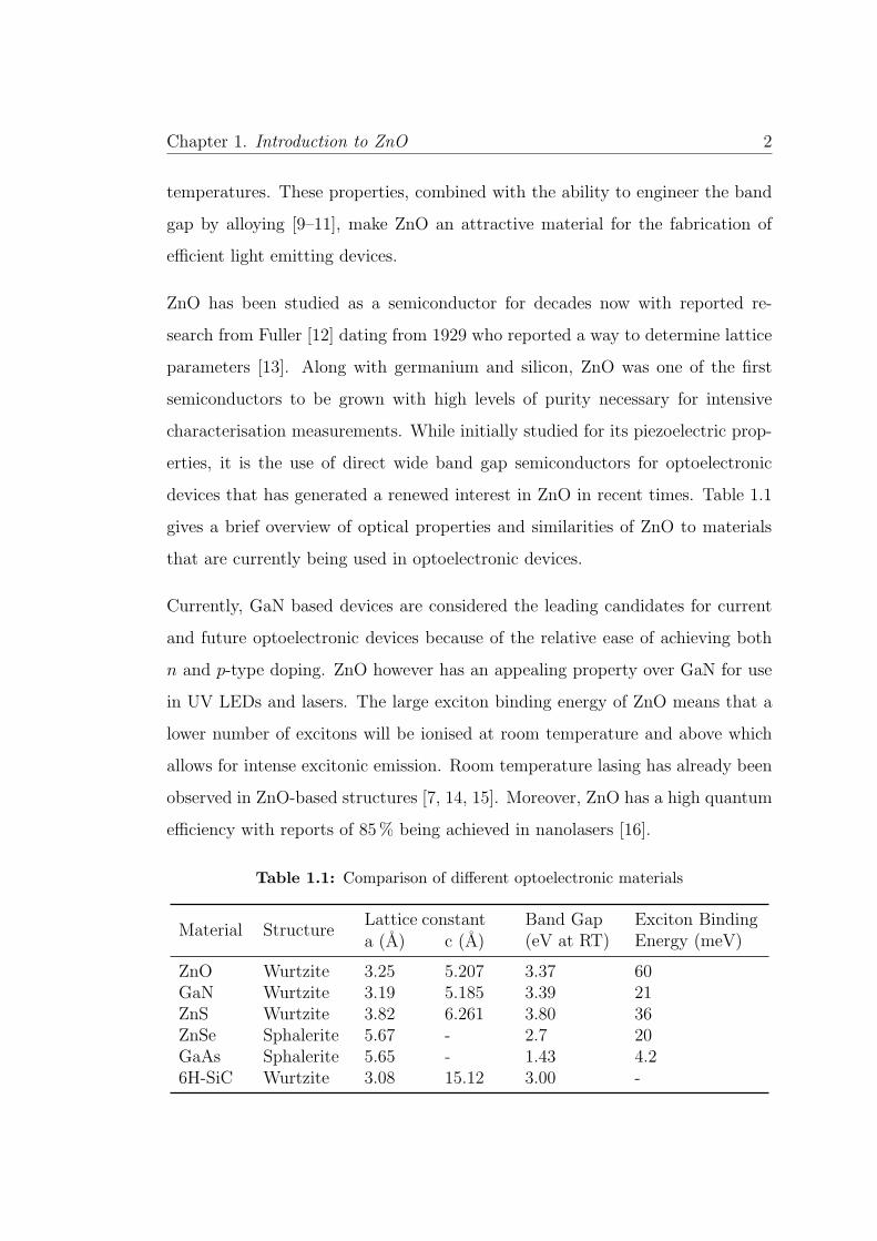
devices that has generated a renewed interest in ZnO in recent times. Table 1.1
gives a brief overview of optical properties and similarities of ZnO to materials
that are currently being used in optoelectronic devices.
Currently, GaN based devices are considered the leading candidates for current
and future optoelectronic devices because of the relative ease of achieving both
n and p-type doping. ZnO however has an appealing property over GaN for use
in UV LEDs and lasers. The large exciton binding energy of ZnO means that a
lower number of excitons will be ionised at room temperature and above which
allows for intense excitonic emission. Room temperature lasing has already been
observed in ZnO-based structures [7, 14, 15]. Moreover, ZnO has a high quantum
efficiency with reports of 85% being achieved in nanolasers [16].
Table 1.1: Comparison of different optoelectronic materials
Material StructureLattice constant Band Gap
(eV at RT)Exciton BindingEnergy (meV)a (A) c (A)
ZnO Wurtzite 3.25 5.207 3.37 60GaN Wurtzite 3.19 5.185 3.39 21ZnS Wurtzite 3.82 6.261 3.80 36ZnSe Sphalerite 5.67 - 2.7 20GaAs Sphalerite 5.65 - 1.43 4.26H-SiC Wurtzite 3.08 15.12 3.00 -

Chapter 1. Introduction to ZnO 3
ZnO also has a high level of radiation resistance [17, 18] which lends ZnO to
development of space application such as transparent conducting oxides for solar
panel uses [19, 20]. Chemical etching, in both acids and alkalis, provides an
opportunity for mass production of small ZnO-based devices. The similarities
between the lattice parameters and structure of ZnO and GaN also suggest that
ZnO can be used as a substrate for high quality epitaxial growth of GaN films.
All these properties make ZnO an attractive material for ultra high efficiency
light emitting sources.
1.2 Motivation of the Research
Despite all the theoretical advantages of ZnO over currently used optical ma-
terials, some fundamental problems still exist. Undoped ZnO is highly n-type.
The origin of this inherent n-type conductivity is still not fully understood. The
origin of this n-type conductivity has been thought to be from native defects,
but recently it is widely believed that accidental incorporation of hydrogen dur-
ing growth to be the cause of this n-type conductivity. Furthermore, achieving
stable p-type ZnO has not been reported yet.
In addition, the luminescence of ZnO typically consists of two emission regions,
one in the UV which is the result of excitonic recombination and one in the visible
which is due to recombination involving deep levels. The visible luminescence is
undesirable for optical materials and also competes with the excitonic emission.
The origin of the broad yellow-green peak often observed in ZnO is typically
attributed to point defects, however the identification of the nature of the defects
involved has been subject to considerable debate for the past 60 years.
Understanding the role of hydrogen as a donor in ZnO and its interaction with
native defects would give more insights into the intrinsic n-type conductivity of

Chapter 1. Introduction to ZnO 4
ZnO, the origin of the deep level emission and also the ability to control those
luminescence centres.
1.3 Aim and Objectives of This Dissertation
The overall aim of this research project is to elucidate the role of hydrogen as a
shallow donor and defect passivator in ZnO. The introduction of hydrogen donors
in ZnO will be investigated with respect to changes in the physical, optical,
chemical and electronic properties when compared to reference samples.
The key objectives of this research work are summarised below:
� Investigate the effects of hydrogen on the luminescence and electronic prop-erties of ZnO.
� Investigate the origin of the deep level emission, specially the origin of thegreen luminescence.
� Investigate the interaction of hydrogen with native defects and impurities.
� Investigate the spatial distribution of luminescence centres and defect re-lated emisions in ZnO.
� Investigate possible shallow carrier traps introduced by plasma.
� Investigate the stability of hydrogen in ZnO.

Chapter 1. Introduction to ZnO 5
1.4 Thesis Structure
This thesis focuses on the study and analysis of the optical and electronic proper-
ties of single crystal ZnO samples. This thesis can be divided into three sections:
� Introduction and background on ZnO - Chapters 1 and 2.
� Experimental details - Chapter 3
� Experimental results - Chapters 4 and 5.
� Conclusions - Chapter 6.
Chapter 1 provides a brief overview in favour of using ZnO for optoelectronic
materials and provided the background to place the work in context. Chap-
ter 2 introduces a comprehensive review of the current knowledge and issues
surrounding the nature of intrinsic defects and impurities and their effects on
the optical properties of ZnO. Chapter 3 describes the various experimental and
sample preparation techniques used throughout this work. Chapter 4 focuses on
the effects of introducing hydrogen impurities in ZnO, specifically on the optical
properties of H-doped ZnO and the chemical state and location of the hydrogen
impurities. Chapter 5 examines the temperature dependence of the luminescence
of ZnO, the possible creation of shallow carrier traps and the stability of hydrogen
in ZnO. Chapter 6 offers a summary of the conclusions and suggestions for future
research directions.
Chapter 2
Defects and Hydrogen Impurities
in ZnO: A Review of Current
Status
This chapter will give an outline of the physical, electronic and optical properties
of ZnO. A detailed review of defects and impurities in ZnO as well as their effects
on the optical properties will be given.
2.1 Physical Properties
ZnO is a II-VI direct wide bandgap semiconductor. A compilation of physical
properties of ZnO is summarised in Table 2.1.
2.2 Crystal Structure
ZnO exists predominantly in the hexagonal wurtzite structure at room temper-
ature and pressure [21]. In this wurtzite structure, zinc ions are tetrahedrally
6

Chapter 2. Defects and Hydrogen Impurities in ZnO 7
Table 2.1: Compilation of some physical properties of ZnO.
Physical Properties Value
Lattice constant
a 3.2496�A
c 5.2065�AMolar mass 81.408 g/molDensity 5.606 g/cm−3
Melting point 1975 ◦C (decomposes)Energy gap 3.37 eV (at 300K)Exciton binding energy 60meVIntrinsic carrier concentration <106 cm−3 (max n-type doping
>1020 cm−3) electronsElectron effective mass m∗
e = 0.24 me
Hole effective mass m∗h = 0.59 me
Hall mobility of electrons at 300K 200 cm2/V s
co-ordinated to four oxygen ions as shown in Figure 2.1 (a). The wurzite struc-
ture actually consists of successive planes composed of tetrahedrally coordinated
Zn2+ and O2− ions stacked along the c-axis. In this wurtzite structure, the unit
cell has a lattice constant of a = 3.296�A and c = 5.207�A [22]. In addtition to the
wurtzite structure, ZnO can also exist in two other crystallographic structures,
the cubic zincblende or rocksalt structures (see Figure 2.1).
There are four surfaces of interest in ZnO, the nonpolar m (1010), the semipolar
a (1120), and the polar (0001)-Zn and (0001)-O surfaces. These polar surfaces
result in spontaneous polarisation along the c-axis and lead to the piezoelectric
properties of ZnO. Surface reconstruction or faceting to stabilise polar surfaces
has not been reported in ZnO. Instead the polar c surfaces are atomically flat
and stable surfaces without any reconstruction [23]. Surface reconstruction will
imply breaking of Zn-O bonds and rearrangement of ions on the surface, which
is energetically unfavourable due to the strong Zn-O bond energy [24].

Chapter 2. Defects and Hydrogen Impurities in ZnO 8
(a) Wurtzite
(b) Zincblende (c) Rocksalt
Figure 2.1: Unit cells for common ZnO structures. Grey spheres repre-sent zinc atoms while red spheres represent oxygen atoms. The wurtzite andzincblende structure are both terminated by the Zn-0001 face.
2.3 Band Structure of ZnO
ZnO is a wide band-gap semiconductor (Eg ≈ 3.37 eV with a high exciton binding
energy of Eb = 60meV. As a direct semiconductor, its highest valence and
lowest conduction band are both located at the Γ-point of the Brillouin zone as
shown in Figure 2.2(a). The conduction band is s-like two-fold degenerated and
comprises of the empty zinc 4s orbital. The valence band is p-like caused by
the fully occupied oxygen 2p orbitals in ZnO [25]. Its 6-fold degeneracy is lifted
due to spin-orbit interaction and due to the crystal field splitting caused by the
anisotropy of the wurtzite structure. Three topmost valence bands are observed.
The assignment of the symmetries to these three bands is still under discussion

Chapter 2. Defects and Hydrogen Impurities in ZnO 9
in literature, but the valence band order Γ7–Γ9–Γ7 corresponding to a negative
Δso has recently become widely accepted [26]. Regardless of the actual valence
band order, the bands are labelled A, B and C with increasing distance to the
conduction band as shown in Figure 2.2(b). This denomination is also used for
the excitons related to these bands. The energetic differences are ΔAB = 4.9 meV
and ΔBC = 43.7 meV [27].
(a) Band Structure (b) Valence band splitting
Figure 2.2: Calculated band structure of ZnO using the HSE hybrid func-tional in (a) (taken from [28]). Splitting of the valence band into the A, B,and C sub-bands caused by the combined effects of crystal-field splitting andspin-orbit coupling in (b) (taken from [27]).
The temperature dependence of the bandgap can be described up to room tem-
perature by the Varshni model [29]:
Eg(T ) = Eg(0)− αT 2
T + β(2.1)
where Eg(T ) is the energy gap at temperature T, Eg(0) is the energy gap at 0K,
α and β are empirically measured constants with values of 5× 10⁻⁴ eV/K and
900K respectively [30].

Chapter 2. Defects and Hydrogen Impurities in ZnO 10
2.4 Crystallographic defects
Crystalline solids, like ZnO, are prone to a variety of defects or imperfections in
the crystal’s lattice. These defects are of importance because they can affect the
material’s properties significantly. Defects in materials can be grouped in the
following categories:
Bulk defects
Bulk defects occur as voids in the crystal lattice where a cluster of atoms are
missing. Bulk defects can also manifest in the form of impurities clustering
together to form regions of different phase.
Planar defects
Planar defects can appear in many forms. Grain boundaries which occur
when the crystallographic direction of the lattice abruptly changes. This is
common in crystal growth when two crystals which grow initially separately
then meet, forming an interface between the two crystallites. Stacking faults
are considered as planar defects. These occur if the stacking pattern of a
closed pack structure is interrupted. Considering the stacking sequence
ABCABCABC being interrupted by one or two layers, this is known as a
stacking fault (ABCABABCAB).
Line defects
There are two types of line defects, edge dislocation and screw dislocation.
Dislocations combining both edge and screw dislocations are also common.
An edge dislocation occurs when one plane of atoms terminates in the
middle of a crystal. This causes the adjacent planes to not be straight,
but instead bend around the edge of the terminating plane. This happens
to preserve the ordering of crystal planes on both sides of the terminating
plane. Screw dislocations are similar, but a helical path is created instead of
an edge. Dislocations often result in lattice distortions. The direction and

Chapter 2. Defects and Hydrogen Impurities in ZnO 11
magnitude of such distortion is expressed in terms of a Burgers vector. For
an edge dislocation, the Burgers vector is perpendicular to the dislocation
line, whereas in the case of the screw dislocation it is parallel. Dislocations
can move if the atoms from one of the surrounding planes break their bonds
and rebond with the atoms at the terminating edge. This leads to the
malleability of materials.
Point defects
Point defects are defects that occur at only one or around one lattice point.
Common point defects are:
� Vacancy
The absence of atom A at its designated position in the lattice, VA.
e.g. zinc vacancy - VZn. Figure 2.3 (a).
� Interstitial
An atom A located between lattice sites, Ai e.g. zinc interstitial Zni.
Figure 2.3 (b).
� Antisite
An atom A being on the lattice spot of atom B, and both A and B
belong to the host material, e.g. OZn or ZnO. Figure 2.3 (c).
� Substitutional
An external atom C being in the lattice site of another host atom, e.g.
LiZn. Figure 2.3 (d).
Point defects are important in semiconductors because they are often identified
as being the cause of various electronic and optical properties.
2.4.1 Vacancies
Vacancies in ZnO, such as zinc (VZn) or oxygen (VO) vacancies, are sites in the
lattice which are usually occupied by an atom, but which is left empty. Vacancies

Chapter 2. Defects and Hydrogen Impurities in ZnO 12
Figure 2.3: Example of point defects in ZnO where grey spheres are zincatoms and red spheres are oxygen atoms. (a) a zinc vacancy VZn, (b) a zincinterstitial Zni, (c) an oxygen antisite OZn, (d) a substitutional impurity at azinc site e.g. LiZn.
can propagate through the lattice when neighbouring atoms move to fill the
vacancy. The stability of the surrounding crystal structure ensures the vacancy
does not collapse.
In ZnO, first-principle calculations have consistently shown that VO is a deep
defect donor, where the 1+ charge state is thermodynamically unstable [31]. The
formation energy of V+O is calculated to be higher than that of V0
O and V2+O for
all values of the Fermi level as shown in Figure 2.4. Evidence of this “negative
U” behaviour of V+O has been reported experimentally by Pfisterer et al. through
DLTS experiments [32]. The stable charge state of the vacancy depends on the
position of the Fermi energy level in the band gap. The vacancy is found in the +2
charge state if the Fermi level is below the 0/2+ transition level or is in the neutral
charge state if the Fermi level is above the 0/2+ transition level. First principle
calculations place this 0/2+ transition level to be around 0.5-0.8 eV above the
valence band maximum [33, 34]. Calculations that allow band gap estimation

Chapter 2. Defects and Hydrogen Impurities in ZnO 13
Figure 2.4: Formation energies of oxygen vacancies in the 0, 1+ and 2+charge states under zinc rich conditions. The formation energy of the 1+charge state is always highest irrespective of Fermi level, indicating that the1+ state is thermodynamicaly not favoured. Taken from [31]
error of local density approximation have estimated the 0/2+ transition level to
be 1-2 eV below the conduction band minimum [35–37]. Calculations disagree on
whether VO should be formed in n-type ZnO, with Lany and Zunger claiming
defect concentration of 1017 cm−3 [38] while Janotti and Van de Walle predict
the formation energy of VO to be too high for significant defect concentration
to be present at equilibrium conditions even in zinc rich conditions [39]. VO has
commonly been attributed as the source of the ubiquitous green luminescence
band centred around 2.4-2.5 eV (approximately 510 nm) [31, 40, 41] due to an
excited-to-ground state transition [42].
A zinc vacancy, VZn, is a double acceptor with first principle calculations placing
the 0/1- and 1-/2- transition levels at respectively 0.1-0.2 and 0.9-1.2 eV above
the valence band maximum [39, 43, 44]. Janotti and Van de Walle [37] pro-
pose that the transition from a shallow donor level to the 1-/2- acceptor level
associated with VZn could result in luminescence around 2.5 eV. Their sugges-
tion is supported by the observation that hydrogen plasma treated ZnO samples

Chapter 2. Defects and Hydrogen Impurities in ZnO 14
show a reduced green luminescence intensity, consistent with VZn passivation by
hydrogen [45].
2.4.2 Interstitials
Interstitial defects occur when an atom occupies a site in the crystal structure at
which an atom would not usually be found. In ZnO, zinc interstitials (Zni) are
shallow donors that have a high formation energy in n-type ZnO [39]. They also
have a migration barrier that can be as low as 0.57 eV, resulting in instability and
high mobility at room temperatures [35]. Being mobile, Zni can form complexes
with impurities such as nitrogen and exist as stable shallow donors [46]. The
formation of Zni is favoured in p-type conditions so this defect is another source
of charge compensation in p-type doping [47].
Oxygen interstitials (Oi) can occupy the octahedral or tetrahedral interstitial
sites or form split interstitials [48]. The octahedral position is unstable and
spontaneously relaxes into a split-interstitial configuration in which Oi shares
a lattice site with one of the nearest oxygen atoms [39]. Oxygen interstitials
occupying the octahedral sites are electrically active and introduce levels in the
band gap that can accept two electrons. Transition levels for the 0/1- and 1-/2-
charge states are at 0.72 and 1.59 eV above the valence band maximum from first
principle calculations [39].
2.4.3 Antisites
Oxygen (OZn) and zinc (ZnO) antisites have high formation energies under all
conditions and are unlikely to form in significant concentrations. ZnO is a double
donor with transitions located within the conduction band. OZn on the other
hand forms deep acceptors with the 0/1- and 1-/2- transition levels at 1.53 eV
and 1.77 eV above the valence band maximum [39].

Chapter 2. Defects and Hydrogen Impurities in ZnO 15
2.4.4 Impurities
Impurities are elements introduced in the lattice which are not atoms of the host
material. Impurities occur as either a substitutional or an interstitial defect.
These impurities can sometimes have different charges compared to the host
atoms and a charge compensation mechanism occurs to keep the overall charge
of the crystal neutral.
Unintentional doping can change the properties of the material by creating donor
or acceptor levels in the band gap of the material. Meyer at al. summarised
some of those defects and the energy levels they create in the band gap [27]. The
additional phtotoluminescence peaks found at liquid helium temperature were
associated to excitons bound to impurities such as hydrogen, gallium, indium
and aluminium (See Table 2.2). The broad visible luminescence centered around
2.4 eV is often attributed to copper impurities which show a distinct fine structure
in the luminescence [49]. The yellow-orange luminescence centered at 2.1 eV has
been attributed to excitons bound to lithium impurities at a zinc substitutional
site [50].
2.4.5 Formation Energies of Native Defects
Understanding the formation energies and processes for defects allows us to make
predictions about the concentration of such defects during growth and processing.
Kohan et al. [43] and Van de Walle [51] have used first principle calculations to
determine the formation energies and electronic structure of the native point
defects in ZnO. In their work, the concentration of a defect within a crystalline
structure depends upon its formation energy (Ef ) as shown in Equation 2.2,
where Nsites represents the concentration of crystal sites where the defect can
occur. The lower the formation energy of a particular defect, the higher its

Chapter 2. Defects and Hydrogen Impurities in ZnO 16
equilibrium concentration.
c = Nsites exp
(− Ef
kBT
)(2.2)
The formation energy of a point defect in a given charge state (q) is given by
Equation 2.3 where Etot(q) represents the total energy loss of a system consisting
of NZn and NO, which represent the number of zinc and oxygen atoms respec-
tively, μZn and μO are the chemical potentials for zinc and oxygen, and EF is the
Fermi energy.
Ef (q) = Etot(q)−NZnμZn −NOμO + qEF (2.3)
The chemical potentials for this relationship rely on the environment conditions
during growth. Under zinc rich and oxygen rich growth conditions, it is possible to
assign bulk chemical potentials to the system (μO = μO(bulk) and μZn = μZn(bulk)).
For intermediate ratios where the system is not particularly zinc or oxygen rich,
μO < μO(bulk) and μZn < μZn(bulk), however the chemical potentials for both zinc
and oxygen are in equilibrium with ZnO: μZn + μO < μZnO.
Native point defects in materials are responsible for the intrinsic electronic and
optical properties. Point defects are most commonly investigated because several
intrinsic defects have low formation energies and tend to form readily during
growth processes. Native defects tend to occur as deep level defects; VO being a
deep donor and VZn being a deep acceptor. Figure 2.5 represents a way to visualise
the location of defects and the probability of them occuring. The formation
energies and charge transition levels were obtained from first principle calculations
[39].
The stable charge state of the defect is dependent on the position of the Fermi level
as well as the growth conditions. Donor type defects growth will be favoured in
zinc rich environments while acceptor type defects will be favoured in oxygen rich
growth environments. Undoped ZnO is normally grown in zinc rich environments
which favour the formation of donors [46].

Chapter 2. Defects and Hydrogen Impurities in ZnO 17
0.0 1.0 2.0 3.0Fermi level (eV)
-2.0
0.0
2.0
4.0
6.0
8.0
10.0
12.0
Form
ationen
ergy
(eV)
0.0 1.0 2.0 3.0Fermi level (eV)
hcir-Ohcir-nZ
VOVZn
Zn iZnO
VZn
Oi(oct)
VO
O i(oct)
OZn
O i(split)
Zn i
ZnO
O i(split)
OZn
Figure 2.5: Formation energies of native defects in ZnO in zinc and oxygenrich environments based on LDA and LDA+U calculations. Slope changesshow charge transition levels. From Janotti and Van de Walle [39]
2.5 Optical Processes in ZnO
Luminescence is the term used to describe radiative emission from a material
following excitation from external energy sources. Luminescence properties in
materials are useful because they give information about defects and defect levels.
Luminescence techniques are usually non-destructive. While there are a variety of
luminescence mechanism, it is worth focusing on two for ZnO. Photoluminescence
(PL) and cathodoluminescence (CL), which differ in the form of excitation. PL
uses photons while CL uses electrons.
Zinc oxide has a characteristic emission spectra comprising of two main peaks:
the NBE emission at 3.3 eV and the broad defect related band occurring at 2.4 eV
as shown in Figure 2.6. The NBE is dominated by FX and D0X emission, along
with LO phonon replicas while the green DLE is attributed usually to native
defect or impurity related recombination mechanisms.
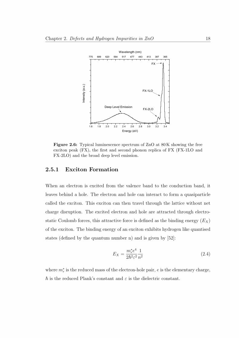
Chapter 2. Defects and Hydrogen Impurities in ZnO 18
1.6 1.8 2.0 2.2 2.4 2.6 2.8 3.0 3.2 3.4
775 689 620 564 517 477 443 413 387 365
FX-2LO
Wavelength (nm)
Inte
nsity
(a.u
.)
Energy (eV)
Deep Level Emission
FX
FX-1LO
Figure 2.6: Typical luminescence spectrum of ZnO at 80K showing the freeexciton peak (FX), the first and second phonon replica of FX (FX-1LO andFX-2LO) and the broad deep level emission.
2.5.1 Exciton Formation
When an electron is excited from the valence band to the conduction band, it
leaves behind a hole. The electron and hole can interact to form a quasiparticle
called the exciton. This exciton can then travel through the lattice without net
charge disruption. The excited electron and hole are attracted through electro-
static Coulomb forces, this attractive force is defined as the binding energy (EX)
of the exciton. The binding energy of an exciton exhibits hydrogen like quantised
states (defined by the quantum number n) and is given by [52]:
EX =m∗
re4
2�2ε21
n2(2.4)
wherem∗r is the reduced mass of the electron-hole pair, e is the elementary charge,
� is the reduced Plank’s constant and ε is the dielectric constant.

Chapter 2. Defects and Hydrogen Impurities in ZnO 19
0 50 100 150 200 250 300 350 400 450 500
50
60
70
80
90
100
Exc
itons
not
ther
mal
ly io
nise
d (%
)
Temperature (K)
ZnO GaN
Figure 2.7: Thermal ionisation of excitons in ZnO and Gan as a functionof temperature from Equation 2.5. At room temperature, 80% of excitonsformed are still bound in ZnO compared to 55% in GaN.
The number of exciton formed is dependent on the exciton binding energy, EX ,
in the material and the temperature according to the Saha equation [53]:
n2eh
nX
=kBT
2π�2μe−EX/kBT (2.5)
where nX is the number of excitons, neh is the number of free carriers and μ is
the reduced effective mass of the electron-hole pair.
Comparing ZnO to GaN, with exciton binding energies of 60meV and 21meV
respectively, ZnO would have a substantially higher percentage of exciton at room
temperature and above as shown in Figure 2.7. The switch to ZnO based devices
from those using GaN would lead to higher emission efficiency.
The excitons created in ZnO correspond to the three levels of the valence band
which is split under crystal field and spin-orbit effects [54]. The excitons corre-
sponding to each level are thus identified as A-, B- and C-excitons in order of
increasing energy gap. The A- and B-excitons are polarised perpendicular to the
c-axis while the C-exciton is polarised parallel to the c-axis [55, 56]. The A- and

Chapter 2. Defects and Hydrogen Impurities in ZnO 20
B-excitons are separated by 4.9meV while the B- and C-exciton separation is
43.7meV (See Section 2.2).
2.5.2 Recombination of electron-hole pairs
In semiconductors there are two types of transitions involving electron-hole pairs
recombination. Radiative recombination during which the electron-hole pair re-
combines and the energy is emitted by a single photon. Non-radiative recombi-
nation is also possible during which photons are not emitted but the energy is
dissipated through quantised lattice vibrations known as phonons.
2.5.3 Radiative Recombination
When an electron is excited from the valence band, it leaves behind a hole. The
electron-hole pair can then recombine radiatively in a number of ways as shown
in Figure 2.8. Once an exciton has formed, it can propagate through the crystal
where it can potentially be trapped by a defect at low temperatures or scattered
by phonons, typically LO phonons. Radiative emission from excitons in ZnO will
only reach the surface of the material if it recombines near the surface due to self
absorption effects.
2.5.3.1 Near Band Edge Emission
The Near Band Edge (NBE) emission in ZnO is radiation emitted in the UV
region. Band to band recombination occurs when a free electron drops from its
excited state in the conduction band to fill an empty free hole state in the valence
band. This results in emission of a photon with an energy equal to that of the
band gap (Figure 2.8 a).

Chapter 2. Defects and Hydrogen Impurities in ZnO 21
EcED ED
EA EA
Eg
Ev
a b c d e f
Ex
Recombination channel Notation Energy of transition
a Excitationb Band to band Eg
c Bound and free exciton [D0X], [A0X], [FX] Eg − EX
d Donor to free hole [D0, h] Eg − ED
e Free electron to acceptor [e, A0] Eg − EA
f Donor-acceptor pair [D0, A0] Eg−ED−EA+q2
4πε0εrr
Figure 2.8: Schematic diagram of the radiative recombination channels pos-sible as a result of an excitation of an electron-hole pair along with the energyof the transition.
While band to band transitions are the simplest recombination mechanism for
an electron hole pair, they are not necessarily the preferential method resulting
in radiative emission. As seen in Figure 2.8, the recombination energy gap can
be reduced by the Coulombic force arising between an electron-hole pair in an
exciton. This can be further reduced through donor or acceptor bound excitons,
reducing the emitted energy from the recombination noticeably. This reduction
in the emission energy gives rise to the NBE peaks observed in opto-electronic
materials such as ZnO.
At liquid helium temperatures, it is possible to separate the narrow NBE band
into individual components, allowing for identification of different impurities and
bound defects. The most prominent lines are labeled as I lines, with In where
n = 0, 1, 2... in order of decreasing energy, following the notation used in early
work on the subject [57]. As the temperature increases, these peaks broaden and
merge, until at room temperature the NBE peak typically only exists as a single

Chapter 2. Defects and Hydrogen Impurities in ZnO 22
Table 2.2: Summary of bound exciton lines in ZnO at low temperature
Line Photon energy (eV) Identified impurity
FX 3.3767 -I0 3.3724 AlI1 3.3711 GaI1a 3.3691 -I2 3.3677 Li, NaI3 3.3664 -I3a 3.3654 Zni
I4 3.3629 HI5 3.3614 -I6 3.3605 AlI6a 3.3604 -I7 3.3600 -I8 3.3597 GaI8a 3.3593 -I9 3.3564 InI10 3.3530 -I11 3.3483 -
Adapted from Meyer et al. [27]
broad emission centred at an energy just below the fundamental band gap. This
is also influenced by the thermal ionisation of the various bound excitons.
There is a considerable amount of controversy regarding the assignment of the I
lines as found in Table 2.2 to various donor or acceptor bound excitons. There
is general consensus, however, that I3-I8 are due to D0X, while I9-I11 have been
suggested as either due to D0X [27] or A0X [58]. The I0-I2 lines have been
attributed to D0X [58, 59] or excitons bound to ionised donors [27]. The study of
bound excitonic luminescence provides information regarding the identity of the
impurities, as well as their relative concentrations, in a given ZnO sample.
2.5.3.2 Deep Level Emission
The emission spectra of ZnO crystals in the visible range is dominated by a broad
luminescence band between 2.9 eV (427 nm) and 1.5 eV (828 nm) with a maximum

Chapter 2. Defects and Hydrogen Impurities in ZnO 23
around 2.35 eV (527 nm). A variety of models have been proposed to explain the
deep level emission from ZnO. This luminescence is found in the visible range
with green, yellow and red luminescences being reported. It is widely accepted
that the emission occurs as the result of either native defects or unintentional
impurities, with point defects such as VO, VZn, or Zni, along with Cu interstitials
or Li on a substitutional Zn site being investigated thoroughly. However, there
is still no conclusive result to identify the origin of the emission.
2.5.3.3 Green Luminescence
The green luminescence in ZnO was fist reported in 1938 by Ewles [60]. Early
studies explicitly attributed the broad green peak to copper impurities [49], how-
ever more recent evidence has suggested the defect was more likely to be related
to intrinsic defects such as VO or VZn. Both defect mechanisms offer plausible ar-
guments, and it has been further proposed that there are two nearly similar, but
fundamentally different, emission characteristics in this region of the spectrum as
a result of both defect models. Experimental evidence shows that copper impuri-
ties tend to result in a fine structure within photoluminescence spectra at liquid
helium temperatures. The transition from (Cu+,h) to the Cu2+ T2 state results
in a photon with the zero-phonon line of the emission at 2.86 eV [61]. Phonon
replicas of this peak, separated by 72 meV (consistent with the longitudinal-
optical phonon mode in ZnO), are responsible for the fine structure of the band
centered at 2.4 eV. In the case of native point defects (VO or VZn) the emission
is a structureless band at the same position with a similar width.
Kohan et al. [43] have calculated the defect formation energy for a variety of native
point defects in ZnO as a function of the Fermi level. Their work concluded that
the two most common defects in ZnO are likely to be vacancies of oxygen or
zinc. The oxygen vacancies have lower formation energy than zinc interstitials,

Chapter 2. Defects and Hydrogen Impurities in ZnO 24
and so are more likely to form in zinc rich growth conditions, while oxygen rich
conditions should yield zinc vacancies.
Other work from Vanheusden et al. has also shown correlations between the con-
centrations of free electrons and VO defects with the intensity of the green band
through EPR measurements [40, 62]. Through annealing experiments under both
oxidizing and reducing environments, strong evidence was provided supporting
VO as the mechanism supporting the origin of the green defect band. This in-
terpretation of the results has come under scrutiny however as the electron para-
magnetic resonance signal (g=1.96) used by Vanheusden to identify the oxygen
vacancies was in fact subsequently found to be related to an isotropic shallow
donor level [63].
More recently, both theoretical and experimental work have been attributing the
structureless green luminescence to native zinc vacancies. VZn has a low formation
energy and hence its concentration in undoped ZnO is expected to be significant.
Calculations also place the -1/-2 transition level of VZn at ≈0.9 eV above the
valence band maximum [39, 43, 64]. A transition involving a free electron in
the conduction band or an electron at a shallow donor to a hole bound to the
singly ionised V−Zn would lead to emission of a photon with an energy of 2.4 eV,
consistent with the green luminescence. An increase in the intensity of the green
luminescence was observed after ZnO was annealed in an oxidising atmosphere
[65]. This is again consistent with the formation of VZn.
2.5.3.4 Yellow Luminescence
In addition to the green luminescence at 2.4 eV, ZnO also exhibits a yellow lu-
minescence centered at 2.1-2.2 eV. This yellow luminescence has been observed
in PL studies of nominally undoped ZnO and has been attributed to excess oxy-
gen in the samples [66], specifically oxygen interstitials (Oi) during hydrothermal
growth processes [67–69]. Other work has attributed the yellow luminescence to

Chapter 2. Defects and Hydrogen Impurities in ZnO 25
lithium impurities [50, 70]. Lithium in the form of LiOH is used as a mineraliser
during hydrothermal growth of ZnO crystals [71–74]. Lithium occupies a zinc site
(LiZn), forming a deep acceptor level 0.8 eV above the valence band maximum
[75]. It is believed that the yellow luminescence is due to a donor-acceptor pair
type transition from a shallow donor to the LiZn acceptor [76]. All hydrother-
mally grown ZnO is expected to exhibit this yellow luminescence owing to the
use of LiOH to dissolve the precursors.
2.5.3.5 Red Luminescence
The red luminescence in ZnO is often associated to excess zinc due its appearance
after annealing ZnO in zinc vapour at 1100◦C [77–79]. It has also been reported
that the red luminescence appears after annealing in atmospheres containing
phosphorous, titanium, iron, nickel or cobalt [79–82]. Recent work shows that
hydrogen may be involved in the red luminescence. Annealing in zinc vapour
in the presence of hydrogen leads to the appearance of the red luminescence,
which is reversible with removal of hydrogen [83]. This suggests that the red
luminescence is a consequence of the interaction between oxygen vacancies and
hydrogen.
2.5.3.6 Summary
The reported origin of the deep level emission are summarised in Table 2.3.
Table 2.3: Summary of deep level emissions in ZnO and frequent assignmentsof its origin
Emission Peak Energy (eV) Origin
Green 2.4 - 2.6 VZn, VO, CuZn
Yellow 2.0 - 2.1 LiZn, Oi
Red 1.7 - 1.9 VO-H, TMZn

Chapter 2. Defects and Hydrogen Impurities in ZnO 26
2.5.4 Non-Radiative Recombination
After an electron is excited from the valence band to higher energy levels, the elec-
tron can then return to its ground state emitting the excess energy. The excess
energy not emitted in the form of photons is called non-radiative recombination.
There are three main physical methods with which non-radiative recombination
can occur: non-radiative via deep level, Auger recombination and surface recom-
bination. Due to a high degree of coupling to lattice vibrations non-radiative
recombination processes are typically thermally activated and can dominate car-
rier relaxation at elevated temperatures.
2.5.4.1 Non-Radiative via Deep Level
Defects in the crystal structure are the most common cause resulting in non-
radiative recombination. Point defects such as impurities, vacancies, interstitials
and antisites introduce new energy levels in the band gap of semiconductors
and can alter the electronic properties of a semiconductor. These energy levels
can act as efficient recombination centres. These levels are often referred to
as traps or luminescence killers owing to their promotion of the non-radiative
processes. Rather than releasing the energy gained through the recombination
of the electron hole pair in the form of light, these defects instead can produce
quantised vibrational quasiparticles known as phonons. These phonons vibrate
through the lattice, dispersing the released energy as heat to the material and
surrounding environment.
2.5.4.2 Auger Recombination
Energy from the recombination can be given to a third carrier which is then
excited to a higher energy level without shifting to another energy band. This
third carrier then normally loses the excess energy to thermal vibrations in the
Chapter 2. Defects and Hydrogen Impurities in ZnO 27
semiconductor. Owing to the need to have a third particle present, Auger recom-
bination is significant only in conditions where the carrier density is very high.
The generation process itself is not easily produced as the third particle would
have to start in the unstable high-energy state.
2.5.4.3 Surface Recombination
A surface is a disruption in the periodicity of the crystal lattice which can then
lead to a change in the band structure at the surface of semiconductors when
compared to the bulk band structure. Atoms at the surface do not have the same
bonding structure as bulk atoms due to the absence of neighbouring atoms. The
surface atoms normally have dangling bonds due to partially unfilled electron or-
bitals. It is these dangling bonds that can act as non-radiative centres producing
phonons rather than photons. It is also however possible to passivate the surface
effects of semiconductors through methods such as shallow doping or growth of
a capping layer on top of the surface.
2.6 Hydrogen in ZnO
Studying the effects of hydrogen in ZnO is important because hydrogen is present
in nearly all crystal growth methods. Hydrogen is present in the form of water in
hydrothermal growth methods and as residual water vapour in CVD chambers.
Hydrogen being a small element and being mobile can easily be incorporated
into the ZnO lattice during growth [84, 85]. It has been suggested that hydro-
gen donors unintentionally incorporated during growth could be the cause of the
strong n-type behaviour of ZnO [86–88]. Several post-growth methods of intro-
ducing hydrogen in ZnO have been reported with the most popular ones being
annealing in a hydrogen atmosphere [89, 90], implantation [91, 92] and exposure
to a hydrogen plasma [45, 85, 93].

Chapter 2. Defects and Hydrogen Impurities in ZnO 28
Figure 2.9: The H+i /H
−i electronic transition level in various semiconductors.
Hi acts as an acceptor if EF is above Et or as a donor if EF is below. In ZnOEt is above the CBM showing that hydrogen is a shallow donor under allconditions and only present as ionized H+
i . From Van de Walle [94].
2.6.1 Hydrogen as a Donor
Interstitial hydrogen (Hi) is an amphoteric impurity in most semiconductors.
Hydrogen forms donors (H+i ) in p-type materials and acceptors (H−i ) in n-type
materials. Figure 2.9 shows the H+i /H
−i energy level for several semiconductors
and shows the amphoteric nature of hydrogen. Hydrogen however only forms
donors in ZnO. First principle calculations predict the formation energy of H+i
to be the most energetically favourable state of hydrogen across the whole band
gap (Figure 2.10) [86]. The main reason for this behaviour is the large strength
of the O−H bond, which drives the formation energy of H+i down. This energy
is low enough to allow for a large solubility of hydrogen and becomes even lower
for Fermi-level positions lower in the band gap as in p-type material.

Chapter 2. Defects and Hydrogen Impurities in ZnO 29
Figure 2.10: Formation energies of interstitial hydrogen in ZnO, as a functionof Fermi level, obtained from DFT-LDA calculations. The formation energy ofH+ is the lowest at every position in the band gap. From Van de Walle [86].
There has been experimental evidence of the donor behaviour of hydrogen through
electrical measurement and infrared absorption spectroscopy. Hall measurement
showed an increase of carrier concentration in ZnO crystals by at least one order
of magnitude after having been exposed to a hydrogen plasma [85, 95]. Ion
implantation of hydrogen showed an increase in the carrier concentration by four
orders of magnitude when compared to the unimplanted one [96]. Annealing
in a hydrogen atmosphere showed a LVM of the O-H bond in ZnO at 3336 cm−1
through infrared absorption spectroscopy [97–99]. The intensity of this absorption
peak increased with annealing time. Electron paramagnetic resonance (EPR)
measurements by Hoffmann et al. [87] exhibited two donor resonances, with one
of the two related to interstitial hydrogen and determined the ionisation energy
of the Hi level to be 35meV.
Photoluminescence experiments reported the appearance or enhancement of a
luminescence peak at 3.363 eV after hydrogen doping [89, 93, 95, 98, 100, 101].
This luminescence peak, called the I4 line, is often associated with an excitonic
recombination involving hydrogen shallow donors (see Section 2.5.3.1).

Chapter 2. Defects and Hydrogen Impurities in ZnO 30
Figure 2.11: Model for Hi in ZnO. Left: ZnO wurtzite structure sites atwhich Hi can incorporate. Right: Anti-Bonding configuration (AB). From Vande Walle [86]
2.6.2 Location of Hydrogen in the Lattice
The position of hydrogen donors in the lattice is still a matter of controversy with
different locations and forms being proposed [102]. Van de Walle [86] proposed
two models for Hi donors shown in Figure 2.11. In one model, H is in the anti-
bonding (AB⊥) orientation, attached to a host O atom and pointing away from
the Zn−O bond. Another model is the bond-centered (BC‖) configuration, where
H sits between the hosts Zn and O. Also possible is the H at the anti-bonding
position of the Zn atom, with the H atom pointing away from the Zn−O bond.
Evidence of these interstitial positions have been found through infrared absorp-
tion measurements. The LVM found at 3336 cm−1 [97, 98, 103] and 3611 cm−1
[98, 99] in hydrogenated ZnO correlate to first principle calculations and have
been assigned to both the AB⊥ and BC‖ configurations respectively. Muon im-
plantation experiments performed by Shimomura et al. [104] found that the BC‖
configuration to be the more stable configuration. This is in agreement with first
priciple calculations [51]. The migration energy barrier of Hi has been found to

Chapter 2. Defects and Hydrogen Impurities in ZnO 31
range from 30meV to 0.5 eV, implying that Hi is mobile at room temperature
[105, 106].
In addition to Hi, other configurations have been studied. Recently, DFT calcu-
lations predict the possibility of HO, hydrogen sitting at an oxygen vacancy site
[37]. The migration energy barrier of HO was calculated to be 1.7 eV [105]. There
is little experimental evidence for this donor, but the high stability of the D0X
emission weeks after hydrogen doping suggests the formation of HO since Hi is
too mobile at room temperature.
The “hidden” hydrogen in ZnO has also been investigated. Shi et al. [98] per-
formed annealing experiments on hydrogen doped ZnO crystals and found that
annealing at temperatures below 300 ◦C causes the carrier concentration to de-
crease. Upon annealing at higher temperatures, the carrier concentration recov-
ered. This was attributed to dissociation of hidden H2 molecules to Hi. Ra-
man spectroscopy showed a LVM at 4145 cm−1 which has been attributed to H2
molecules being formed from migration and recombination of Hi [90].
2.6.3 Interaction of Hydrogen With Defects
In addition to forming shallow donors in ZnO, hydrogen can also interact with
defects. Hall measurements showed an increase in both the carrier concentration
and carrier mobility after hydrogen doping [107, 108]. Higher carrier concen-
tration usually leads to a strong carrier scattering and the mobility would be
decreased because of the increasing carrier scattering. The observed increase
in both mobility and carrier concentration suggests that a substantial fraction of
the incorporated hydrogen passivates defects at grain boundaries and/or acceptor
impurities.
Luminescence measurements done on hydrogen doped ZnO showed a decrease in
the deep level luminescence which is associated to recombination at defect centres

Chapter 2. Defects and Hydrogen Impurities in ZnO 32
after hydrogen doping. CL and PL measurements done on hydrogen doped ZnO
crystals showed a quenching of the green luminescence as well as an enhance-
ment of the NBE emission after doping [45, 95, 101, 109]. It has been suggested
that hydrogen passivates defects that are responsible for the green luminescence,
namely VZn, by forming neutral VZn-H2 complexes, thereby quenching the green
luminescence.
Evidence of such a complex was reported by Lavrov et al. through infrared ab-
sorption spectroscopy [99]. Two absorption lines at 3349.6 cm−1 and 3312 cm−1
appeared after hydrogen doping which corresponds to the O−H bond vibrational
modes. These lines were associated to a defect that contains two hydrogen atoms,
one in an O−H bond roughly aligned with the c-axis, and the other in an O−Hthat forms an angle of 100� with the c-axis. These observations matched first-
principles calculations for a hydrogenated Zn vacancy (VZn-H2).

Chapter 3
Experimental Details
This chapter briefly describes the key experimental techniques used in this project
to modify and characterise ZnO. Electronic grade ZnO crystals obtained from the
MTI Corporation were used in this project. The crystals were then doped with
hydrogen through a hydrogen plasma exposure. The as-received and hydrogen
doped samples were characterised by complimentary techniques which study the
morphology, optical, electronic and chemical properties of the ZnO crystals.
3.1 ZnO Crystal Specimen
ZnO crystals cut in the a-(1120) plane and polished on both sides were obtained
from the MTI Corporation, USA. Crystals from this manufacturer were chosen
because of their common hydrothermal growth method which yields crystals with
high crystallinity and low impurity levels. Figure 3.1 shows a photograph of the
as-received crystals. Manufacturer specifications for the crystals are listed in
Table 3.1.
33

Chapter 3. Experimental Details 34
Figure 3.1: Photograph of a-plane ZnO crystal obtained from MTI Corpora-tion. Also shown is a ruler showing the 10× 10 mm dimensions of the crystal.
Table 3.1: ZnO single crystal substrate supplied by MTI Corporation.
Purity wt% >99.99Impurity wt% Li : 0.0001 − 0.001; Mg: <0.0005; Al :
<0.0030; Si : 0.0030; Ti : 0.0010; Cu:<0.0030; Fe: <0.0050; Ca: <0.0005;Ag: <0.0002
Crystal structure Hexagonal: a=3.252 A, c=5.313 AGrowth method HydrothermalHardness 4 (Mohs scale)Density 5.7 g/cm3
Melt point 1975 ◦CSpecific heat 0.125 cal/gThermoelectric constant 1200mV/K at 300 ◦CThermal conductivity 0.006 cal/cm/KThermal expansion 2.90× 10⁻⁶/KTransmission range 0.4 - 0.6 m > 50% at 2 mmDislocation density <0001> plane < 100 / cm2

Chapter 3. Experimental Details 35
3.2 Sample Cleaning and Preparation
The ZnO crystals were cut to the required size using a diamond pen. The smaller
pieces were cleaned in the following way :
� 15 minutes ultrasonic bath in acetone� 15 minutes ultrasonic bath in isopropyl alcohol
� 15 minutes ultrasonic bath in deionised water� Nitrogen gas blow dry
Annealing of ZnO crystals was done in a Lindberg/Blue single zone tube furnace.
The furnace allows annealing at temperatures up to 1100 ◦C under vacuum or
controlled gaseous environments.
3.3 Hydrogen Doping
Hydrogen plasma treatment was done through an R.F plasma. A custom built
plasma reactor was assembled for doping ZnO. The basic setup is illustrated
in Figure 3.2. Hydrogen gas is flown into the evacuated chamber moderated
using an Apex mass flow controller. A constant pressure is monitored with a
Lam research series capacitance diaphragm gauge. Plasma is generated using an
AG 0202-HV OS high voltage plasma generator from T&C Power Conversion,
Inc. Hydrogen gas is ionised creating energetic radicals which penetrate into
the sample and diffuse. The sample was heated during treatment to encourage
diffusion of hydrogen.
It was found that hydrogen can be incorporated in ZnO in the range of 25 ◦C to
450 ◦C and in a time as low as 10 s. Optimal parameters for the plasma cycle
consisted of heating the clean ZnO sample in an evacuated chamber (10−1Torr)
to 200 ◦C. RF power of 15W was used with 10 sccm H2 flow rate to create
hydrogen radicals. After plasma treatments the sample was cooled in a hydrogen
atmosphere to room temperature before removal from the chamber for analysis.

Chapter 3. Experimental Details 36
Heater 200oC
H2 Inlet10 sccm
Pump
ZnOsubstrate
H2 2H.
RF Signal Generator15 W
0.1 torr
Figure 3.2: Photograph (left) and schematic (right) of the plasma chamberused for H-doping of ZnO crystals identifying key features.
3.4 Scanning Electron Microscopy (SEM)
Scanning electron microscopy (SEM) has been used to assess the morphology of
the samples before optical and electrical characterisation as well as any possible
surface damage caused by the doping procedure.
In a typical SEM (Figure 3.3), electrons are emitted from a heated filament and
accelerated towards the anode with energy ranging from 100 eV to 30 keV. The
electron beam is then focused by the condenser and objective lens to form a
narrow beam with a diameter of the order of nanometres on the sample surface.
This beam passes through scanning coils which deflect the beam in a raster
pattern over an area of the sample surface.
Interaction of the primary beam with matter in an SEM can lead to a series of
scattering processes. High energy electrons interacting with matter can lead to
the generation of backscattered electrons, secondary electrons, X-rays, or light
(Figure 3.4). Each emission gives information about the sample, e.g. secondary
electrons give a topographical image of the sample surface, backscattered elec-
trons give spatial information dependent on compositions, X-rays give the chem-
ical composition and concentration of elements, while the light emitted gives

Chapter 3. Experimental Details 37
To Computer
Condenser Lens
Scanning Coils
Objective Lens
Objective LensAperture
Sample
FilamentAnode
ScanGenerator
Secondary ElectronDetector
Primary Electron BeamSecondary Electrons
Figure 3.3: Schematic diagram showing key parts of a typical SEM.
X-rays
Backscatteredelectrons
CL
Secondaryelectrons
Electron beam
Figure 3.4: Processes induced by electron bombardment.
information about defects in the sample.
In this work an FEI Quanta 200 ESEM was used for electron beam analysis of
ZnO. The spatial resolution of the microscope is 3.0 nm at 30 keV or 10 nm at
3 keV. The operating pressure inside the microscope chamber was <10−5Torr.
Beam current was measured by using a Faraday cup. The Faraday cup consisted
of a hole drilled in the specimen holders. The beam is focused into the aperture
and the cavity under the aperture absorbs virtually all electrons from the main

Chapter 3. Experimental Details 38
beam. The stage is then connected to an ammeter to measure and display the
absorbed current.
3.5 Cathodoluminescence Spectroscopy
Cathodoluminescence (CL) is the light emitted through the recombination of
electron-hole pairs following excitement by a focused electron beam. CL occurs
through the radiative recombination of electron-hole pairs produced after irradi-
ation from an electron beam (See Section 2.5.3 for a detailed description of the
generation and recombination processes). CL is a powerful investigative tool that
can examine the optical properties of materials in a non-invasive manner. CL can
obtain resolution below that of the diffraction limit of light. The technique can
be used to characterise the composition and defects of a material.
The spatial resolution of CL is strongly determined by the interaction volume of
the electrons incident on the material. In this volume, the electrons undergo a
series of elastic and inelastic scattering events, which can result in electron-hole
pair generation leading to CL. The maximum range (Re) for an electron can be
approximated by using the Kanaya and Okayama equation [110]:
Re(�m) =0.0276AE1.67
b
ρZ0.889e
(3.1)
where Eb is the accelerating voltage of the electron beam in keV, A is the atomic
weight of the material in g/mol, ρ is the material density in g/cm3 and Ze is the
effective atomic number. Ze can be calculated by using a weighted average of the
atomic numbers of the constituent atoms such as:
Ze = AZn
AZnO× ZZn +
AO
AZnO× ZO
= 65.3881.39
× 30 + 16.0181.39
× 8
= 25.67
(3.2)
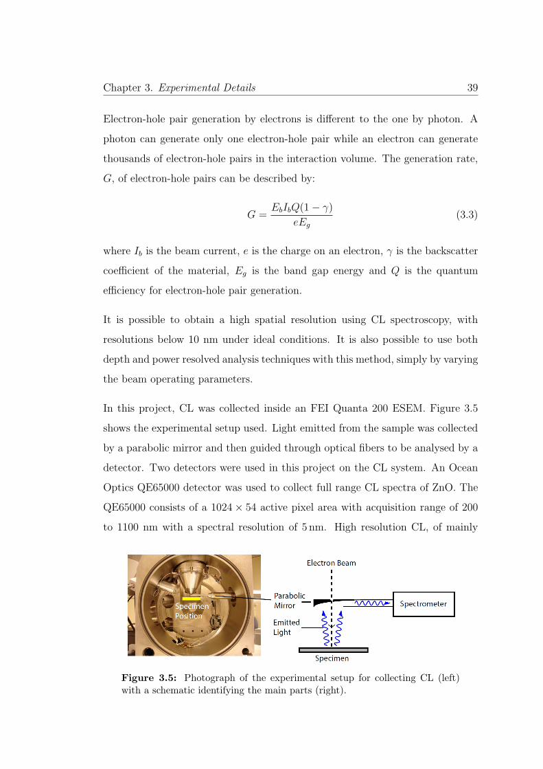
Chapter 3. Experimental Details 39
Electron-hole pair generation by electrons is different to the one by photon. A
photon can generate only one electron-hole pair while an electron can generate
thousands of electron-hole pairs in the interaction volume. The generation rate,
G, of electron-hole pairs can be described by:
G =EbIbQ(1− γ)
eEg
(3.3)
where Ib is the beam current, e is the charge on an electron, γ is the backscatter
coefficient of the material, Eg is the band gap energy and Q is the quantum
efficiency for electron-hole pair generation.
It is possible to obtain a high spatial resolution using CL spectroscopy, with
resolutions below 10 nm under ideal conditions. It is also possible to use both
depth and power resolved analysis techniques with this method, simply by varying
the beam operating parameters.
In this project, CL was collected inside an FEI Quanta 200 ESEM. Figure 3.5
shows the experimental setup used. Light emitted from the sample was collected
by a parabolic mirror and then guided through optical fibers to be analysed by a
detector. Two detectors were used in this project on the CL system. An Ocean
Optics QE65000 detector was used to collect full range CL spectra of ZnO. The
QE65000 consists of a 1024× 54 active pixel area with acquisition range of 200
to 1100 nm with a spectral resolution of 5 nm. High resolution CL, of mainly
Figure 3.5: Photograph of the experimental setup for collecting CL (left)with a schematic identifying the main parts (right).

Chapter 3. Experimental Details 40
the near band edge region of ZnO, was collected with a Hamamatsu S7011-1007
CCD sensor which consists of 1044× 124 active pixels. The sensor was housed
inside a Hamamatsu C7021 detector head. The light was dispersed in an Oriel
MS 257 1⁄4m monochromator by a 1200 lines/mm grating. This setup allowed for
a spectral resolution of 0.1 nm over a 53 nm range.
Temperature dependent CL was achieved using three SEM cooling/heating stages.
A Gatan C1002 liquid nitrogen cold stage was used for cooling samples down to
80K and a Gatan CF302 continuous flow liquid helium cold stage for cooling to
5K. High temperature CL up to 500 ◦C was performed on a custom built heater
stage.
3.5.1 CL System Calibration
All CL spectra taken were calibrated for the response of the system in both in-
tensity and wavelength. An Oriel 63355 200W QTH calibrated lamp of known
spectral profile was used for intensity calibration. The correction curve was ob-
tained according to the following equation:
Correction curve =Normalised reference intensity
Normalised measured intensity(3.4)
Figure 3.6 shows the measured intensity as a function of wavelength as well as
the reference emission spectrum of the lamp provided by Oriel and the calculated
correction curve. The peaks in the correction curve at 400 nm and above 900 nm
are caused by absorption of the light by the optical fiber.
Calibration for high resolution CL spectral analysis (resolution of 0.1 nm) was
achieved by measuring atomic spectral lines of mercury or neon immediately after
the acquisition of the ZnO spectra. Figure 3.7 shows CL spectra of a mercury
and a neon lamp as well as the calculated wavelength calibration curve. The

Chapter 3. Experimental Details 41
300 400 500 600 700 800 900 10000.0
0.1
0.2
0.3
0.4
0.5
0.6
0.7
0.8
0.9
1.0
Inte
nsity
(a.u
.)
Wavelength (nm)
Measured curve Standard curve
(a) Measured intensity curve
300 400 500 600 700 800 900 10000.0
0.5
1.0
1.5
2.0
2.5
3.0
3.5
Cor
rect
ion
(a.u
.)
Wavelength (nm)
(b) Correction curve
Figure 3.6: (a) CL spectrum of the lamp taken through the CL system usingthe Ocean Optics QE65000 detector and the emission spectrum of the lamp.(b) The correction curve obtained according to Equation 3.4.
calibrated wavelength was converted into electron volts using the relation:
Photon energy (eV) =1239.841856
λ (nm)(3.5)
Since the spectrometers measure photons per sec in a Δnm interval in λ, I(λ)
the measured intensity in eV, I(eV) needs to be corrected to have equal steps in
ΔeV by multiplying I(λ) by λ2.
0 200 400 600 800 1000
MercuryNeon
Inte
nsity
(a.u
)
Pixel
(a) Standard lines
0 200 400 600 800 1000
360
370
380
390
400
410
Wav
elen
gth
(nm
)
Pixel
(b) Calibration curve
Figure 3.7: (a) Mercury and neon spectral lines and (b) wavelength calibra-tion curve.

Chapter 3. Experimental Details 42
3.6 Monte Carlo Simulations (CASINO)
The electron range in a solid can be determined from Equation 3.1. This is
however an approximation and it is more useful to consider the overall interac-
tion volume of electrons with the material. One method is to use a Monte Carlo
simulation package such as CASINO (monte CArlo SImulation of electroN trajec-
tory in sOlids) to determine the actual interaction volume and hence penetration
range of electrons [111]. CASINO is a single scattering Monte Carlo simulation
specifically developed for low electron energy beam interactions (0.1 to 30 keV).
It can generate various signals produced in normal SEM operation such as X-ray
generation, backscattered and secondary electrons as well as CL signals.
CASINO implements Monte Carlo methods in which elastic scattering events
are modeled explicitly using random numbers generated with weighting factors
to produce an appropriate statistical distribution of scattering events. The first
step in the simulation of an elastic collision is to determine which atomic species
is involved. This is calculated based on the atomic fraction and experimentally
determined cross-section of each element in the material.
Random >n∑
i=1
Fiσi∑nj=1 Fjσj
(3.6)
where Random is a random number uniformly distributed between 0 and 1, σi
is the cross section of element i, Fi is the atomic fraction of element i and n
is the number of elements in the region. When the inequality above is true,
the element responsible for the collision is element i. The scattering angle and
distance travelled between collisions are calculated based on material properties
and randomly generated numbers. Inelastic scattering is not simulated explicitly,
instead a continuous slowing down approximation is applied in which an electron
gradually loses energy over the distance travelled between collisions (L). Using

Chapter 3. Experimental Details 43
this approach, the energy of a simulated electron at a given position is
Ei = Ei−1 +dE
dS× L (3.7)
where Ei and Ei−1 are the respective energies at the current and previous col-
lisions and dE/dS is the rate of energy loss measured in keV/nm. The rate of
energy loss is material dependent and represents an averaging of inelastic scat-
tering events over the distance travelled.
CASINO is also able to take minority carrier diffusion into account which has
a significant effect on the size of the interaction volume, specially at low beam
energies (Eb <15 keV) where the carrier diffusion length is of the order of the
electron penetration depth. For ZnO, the carrier diffusion length is ∼90 nm [6].
The interaction volume is in a teardrop shape for no diffusion with the majority
of electrons being deposited and CL generated in the first 17 nm below the surface
as in Figure 3.8(a). While the depth of electrons injected in the sample does not
change, the interaction volume is enlarged when carrier diffusion is taken into
account and the depth profile of CL generated changes. The majority of CL is
generated in 10 to 35 nm from the surface depending on the diffusion models used
(Figure 3.8(b)-3.8(d)).
The parameters used for CASINO simulations used in this project are given in
Table 3.2.

Chapter 3. Experimental Details 44
(a) Prior to diffusion (b) Diffusion - Infinite carrier surface recombination
(c) Diffusion - Carrier surface recombination modelledas a perfect sink
(d) Diffusion - Carrier surface recombination modelledas a reflector
Figure 3.8: Influence of carrier diffusion models on the interaction volumein bulk ZnO. Beam energy was 1 keV with 500,000 electrons simulated. Thevertical distance is the same in all 4 figures.
Table 3.2: CASINO simulation parameters for depth approximations.
Parameter Setting
Sample ZnO substrateDensity 3.998 38 g/cm3
Weight fraction (Zn:O) 0.803 397 : 0.196 603Beam energies 0.1 – 30 keV (0.1 keV steps
to 1 keV then 1 keV steps)Number of simulated electrons 500 000Beam radius 1 nmTotal Cross Section Mott by InterpolationPartial Cross Section Mott by InterpolationEffective Section Ionisation CasnatiIonisation Potential Joy & Luo [1989]Random Number Generator Press et al. [1986]Directing Cosin Soum et al. [1979]dE/dS Calculation Joy & Luo [1989]

Chapter 3. Experimental Details 45
3.7 Electrical Measurements
Electrical measurements were performed by the Van der Pauw method [112]. This
technique allows measurements of resistivity, sheet carrier density of the majority
carrier and mobility of the majority carrier. The main advantage of the Van der
Pauw method is the ability to measure the properties of samples of any arbitrary
shape, as long as the thickness of the sample is less that its length or width.
Ohmic contacts on ZnO crystals were made by dipping the end of a thin wire
into molten indium and rapidly bringing a tiny amount of molten indium on the
wire to the corners of the crystals before the indium solidifies. The contacts were
labeled A, B, C and D as in Figure 3.9.
A
B C
D
IndiumContact
Figure 3.9: Van der Pauw setup for resistivity and Hall measurements.
3.7.1 Resistivity Measurement
A current is flowed along one edge of the sample, IAB and the voltage across the
opposite edge, VCD is measured. The resistance can then be found from Ohm’s
law:
RAB,CD =VCD
IAB
(3.8)
The sheet resistance, Rs, can then be calculated from two of those resistances,
one along the vertical edge (RAB,CD) and one along the horizontal edge (RBC,DA)

Chapter 3. Experimental Details 46
by using the Van der Pauw equation:
exp
(−πRAB,CD
Rs
)+ exp
(−πRBC,DA
Rs
)= 1 (3.9)
For more accurate measurements, reciprocal measurements RCD,AB and RDA,BC
can be taken and the average resistance along the vertical and horizontal edges
calculated. The Van der Pauw formula then becomes:
exp
(−πRvertical
Rs
)+ exp
(−πRhorizontal
Rs
)= 1 (3.10)
The resistivity, ρ, of the sample of thickness, t, is then found by:
ρ = Rs × t (3.11)
3.7.2 Hall Measurement
Hall measurements were performed using the same setup for the resistivity mea-
surements. First, current was passed through opposite corners, IAC , while the
voltage across VBD was measured for a range of current IAC . This was repeated
with a magnetic field, B, applied perpendicular to the surface of the sample. The
voltage VBD was then taken for a series of current again. The difference between
the voltages taken is the Hall voltage, VH . For more accurate results, the mag-
netic field direction can be reversed and the average of the Hall voltages taken.
The carrier concentration, n, can then be found using:
n =BI
eVH
(3.12)

Chapter 3. Experimental Details 47
where e is the elementary charge. From the measured resistivity and the carrier
concentration, the mobility, μ, of the carriers can be calculated using:
μ =1
enRs
(3.13)
3.8 Synchrotron Light Experiments
Synchrotron radiation is electromagnetic radiation emitted as a result of the
change of the trajectory of a high speed electron moving through a magnetic
field. Synchrotron radiation provides radiation ranging from the ultraviolet to
high energy X-rays with intensity several orders of magnitude greater than con-
ventional sources (105 to 106 times greater), along with the ability to tune the
source to selected energies. The light is also highly polarised. The use of high
energy radiation induces a photoelectric response in a sample. This results in the
emission of photoelectrons or other types of radiation that have characteristics
dependent on their original electronic states. Synchrotron light experiments were
performed at the Soft X-ray Beamline of the Australian Synchrotron [113].
3.8.1 X-Ray Photoelectron Spectroscopy
X-ray photoelectron spectroscopy (XPS) analysis is accomplished by irradiating
a sample with monochromatic soft x-ray photons and analysing the energy of the
detected electrons that are emitted from the sample. Using XPS, the chemical
identity and concentration of elements in the sample can be determined by com-
paring the known binding energies of the elements Eb with those deduced from
the kinetic energies of the emitted electrons Ek
Eb = hω − Ek − φd (3.14)

Chapter 3. Experimental Details 48
where hω is the energy of the X-ray photon, and φd is the work function of the
detector.
Another advantage of performing XPS measurements at synchrotron facilities is
the energy of the X-ray photons can be finely tuned. Common laboratory XPS
setups use aluminium or magnesium targets as X-ray source with photon energies
of 1486.6 eV (Al Kα) or 1253.6 eV (Mg Kα). Photon energy ranging from 90 eV to
1500 eV was available for use at the Australian Synchrotron facility. This allowed
for optimising the XPS signal for a particular photoemission by choosing the
appropriate photon energy. Figure 3.10 shows the photoionisation cross sections
for zinc, oxygen and lithium photoemissions [114]. The cross section for Li 1s is 3
orders of magnitude higher with photon energies of 150 eV compared to common
laboratory sources.
0 200 400 600 800 1000 1200 1400
10-3
10-2
10-1
100
Cro
ssse
ctio
n
Photon Energy (eV)
Li 1sO 1sZn 2p
Figure 3.10: X-ray photoionisation cross sections for Zn 2p, O 1s and Li 1sphotoelectrons. The cross section for Li 1s is 3 orders of magnitude higherwith photon energies of 150 eV compared to common laboratory sources.Data taken from [114].
The penetration power of X-ray photons in solids is of the order of 1 �m to 10 �m.
However, the electron interaction with matter is higher than that of photons. This
higher interaction means that the mean free path of electrons is only of the order

Chapter 3. Experimental Details 49
of tens of angstroms. Only photoelectrons which are generated directly below the
surface can leave the surface and contribute to the XPS signal. XPS is therefore
a highly surface sensitive analysis technique.
3.8.2 X-Ray Absorption Near Edge Spectroscopy
X-ray absorption near edge spectroscopy (XANES) measures the absorption of
X-rays as a function of X-ray photon energy. XANES is used to determine the
oxidation state and coordination number of elements in a material, as well as the
site symmetry of the elements. XANES also gives information on the conduction
band of the materials because it is probing empty states. The X-ray photon
energy is scanned over the energy of core levels of the constituent elements of
the sample. An electron is excited from its level and a hole is left. An electron
from a higher energy state will fall into this vacancy and releases the energy in
the form of a photon or further excite an electron from a higher state to form an
Auger electron.
A XANES spectrum shows a typical oscillatory fine structure shape which extends
over hundreds of electron volts above the main absorption edge. Those peaks
correspond to internal electron transitions between core levels. This oscillation
arises due to the wave nature of the emitted photoelectron. Scattering between
the photoelectron and neighbouring atoms causes a standing wave to be formed
which is then reflected by the oscillations in the XANES spectrum.
XANES was performed in two configurations, total electron yield (TEY) and
total fluorescence yield (TFY). TEY is performed when the sample is connected
to ground through an ammeter and the neutralization current is monitored while
TFY measures photons that are emitted after electrons of lower binding energy
fill the created core hole.

Chapter 3. Experimental Details 50
3.9 Raman Spectroscopy
Raman spectroscopy is used to observe vibrational, rotational and low-frequency
modes in a material. Raman spectroscopy works on the principle of inelastic
scattering of monochromatic light by the vibrational modes of the material. The
incoming photon can lose energy due to excitation of rotational, vibrational or
electric states. The photon can also gain energy when an excited mode releases
energy to the photon and relaxes to lower energy levels. These processes are
called Stokes and anti-Stokes Raman scattering respectively. If the change in
the scattering occurs in quantised energy levels, the transitions appear as dis-
tinct lines in the spectrum which are separated from the laser frequency by a
characteristic Raman shift to lower or higher energies.
The wurtzite structure of ZnO with the space group C46v(P63mc) has n = 4
atoms in the primitive unit cell which leads to 3n = 12 vibrational eigenmodes
(3 acoustic and 9 optical modes). These modes are classified according to the
following irreductible representations [115, 116]:
Γ = 2A1(1) + 2B1(1) + 2E1(2) + 2E2(2) (3.15)
This summation corresponds to 12 modes because of the one-fold degeneracy of
the A and B modes and the two-fold E modes. The three acoustic phonon modes
consist of one A1 mode and one E1 mode pair, the other nine modes are optical
modes:
Γopt = A1(1) + Blow1 (1) +Bhigh
1 (1) + E1(2) + Elow2 (2) + Ehigh
2 (2) (3.16)
Figure 3.11 displays a schematic of the displacement of the six optical phonon
modes. The displacements for the A1 and B1 modes are directed along the c-axis
while the E1 and E2 modes are perpendicular to the c-axis. The E modes oscillate

Chapter 3. Experimental Details 51
Figure 3.11: Schematic illustrations of the ion displacements of opticalphonon modes in ZnO. The larger arrows represent the dominant displace-ment vectors. The A1, B
high1 , E1 and Ehigh
2 are oxygen-dominated while theBlow
1 and Elow2 modes are dominated by the zinc displacements. Adapted from
[117]
linearly and independently in the directions perpendicular to the c-axis with the
same energy which leads to the two-fold degeneracy of the E1 and E2 modes.
The A1 and E1 modes consist of oscillations of the rigid Zn sublattice vs. the O
sublattice which result in an oscillating polarisation. The polarity induced macro-
scopic electric fields split these polar modes into longitudinal optical (LO) modes
with an ion displacement parallel to the phonon propagation vector and transver-
sal optical (TO) modes with perpendicular displacement vectors. In contrast to
the A1 and E1 Raman modes, the B1 and E2 modes are non-polar and as such do
not exhibit LO-TO splitting. No polarisation is induced for the B modes since
one sublattice is at rest while the atoms in the neighbouring other sublattices
move opposite each other. Similarly in the E2 modes, the non-polar character of
the vibration is caused by the mutual compensation of the displacement in each
sublattice.
Raman measurements were performed in a Renishaw inVia Raman spectrometer
system equipped with a Leica DMLB microscope and a red Renishaw helium
neon laser source with emission wavelength of 633 nm and power of 17mW.
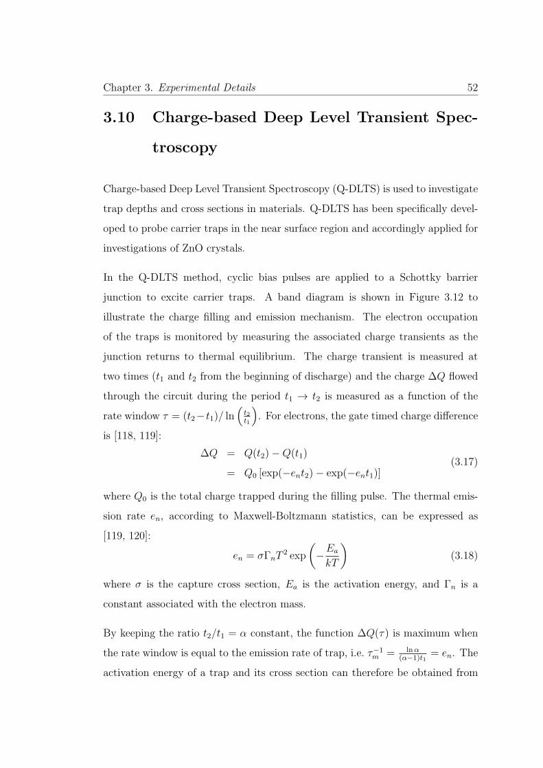
Chapter 3. Experimental Details 52
3.10 Charge-based Deep Level Transient Spec-
troscopy
Charge-based Deep Level Transient Spectroscopy (Q-DLTS) is used to investigate
trap depths and cross sections in materials. Q-DLTS has been specifically devel-
oped to probe carrier traps in the near surface region and accordingly applied for
investigations of ZnO crystals.
In the Q-DLTS method, cyclic bias pulses are applied to a Schottky barrier
junction to excite carrier traps. A band diagram is shown in Figure 3.12 to
illustrate the charge filling and emission mechanism. The electron occupation
of the traps is monitored by measuring the associated charge transients as the
junction returns to thermal equilibrium. The charge transient is measured at
two times (t1 and t2 from the beginning of discharge) and the charge ΔQ flowed
through the circuit during the period t1 → t2 is measured as a function of the
rate window τ = (t2−t1)/ ln(
t2t1
). For electrons, the gate timed charge difference
is [118, 119]:
ΔQ = Q(t2)−Q(t1)
= Q0 [exp(−ent2)− exp(−ent1)](3.17)
where Q0 is the total charge trapped during the filling pulse. The thermal emis-
sion rate en, according to Maxwell-Boltzmann statistics, can be expressed as
[119, 120]:
en = σΓnT2 exp
(−Ea
kT
)(3.18)
where σ is the capture cross section, Ea is the activation energy, and Γn is a
constant associated with the electron mass.
By keeping the ratio t2/t1 = α constant, the function ΔQ(τ) is maximum when
the rate window is equal to the emission rate of trap, i.e. τ−1m = lnα(α−1)t1 = en. The
activation energy of a trap and its cross section can therefore be obtained from

Chapter 3. Experimental Details 53
ConductionBand
Valence Band
Trap state Trap state
(a) Filling (b) Emission
Figure 3.12: Band diagram showing the (a) trap filling and (b) emissionprocesses.
an Arrhenius plot of Equation 3.18, whereas the trap density can be calculated
from the maximum ΔQmax.
A gold Schottky contact pad with a thickness of 150 nm was deposited by evapo-
ration on one face of the ZnO crystal through a shadow mask, while indium ohmic
contact was established on the opposite face as shown in Figure 3.13. Current-
voltage and isothermal Q-DLTS measurements were conducted in vacuum using
the ASMEC-02 system, supplied by InOmTech Inc.
ZnO crystal
InAu
Figure 3.13: Schematic illustration of the DLTS setup showing contacts.

Chapter 3. Experimental Details 54
3.11 Other Characterisation Techniques
In addition to the techniques described in this chapter, the following characteri-
sation tools were also used to study the crystal morphology and optical properties
of the ZnO crystals:
X-Ray Diffraction
X-Ray Diffraction (XRD) was performed on a Siemens D5000 X-ray Diffrac-
tometer. The diffractometer uses copper K-alpha radiation with a wave-
length of 1.5418�A. The XRD was operated in θ − 2θ mode.
Atomic Force Microscopy
Atomic Force Microscopy (AFM) measurements were performed on a Digi-
tal Instruments Dimension 3100 AFM. AFM was used to investigate surface
morphology and mean surface roughness.
Photoluminescence
Photoluminescence (PL) measurements were performed in a liquid helium
bath cryostat which allows measurements from 7K to 300K. The samples
are excited by the 325 nm emission line of a HeCd laser and the emitted light
was dispersed by a Spex-1404 double monochromator (spectral resolution
50 �eV) and detected by a bi-alkali photodetector.

Chapter 4
Hydrogen Doped ZnO
4.1 Introduction
Hydrogen can have a significant effect on the optical and electrical properties of
ZnO. In this project hydrogen was incorporated into ZnO crystals by exposing
ZnO to mild hydrogen plasma. The main advantage of plasma treatment over
other hydrogen doping methods, such as thermal annealing in a hydrogen atmo-
sphere, is that ZnO can be kept at relatively low temperatures. In this project
the sample temperature was kept below 500 ◦C, at which the thermal energy is
considerably lower than the formation energies of native defects reported to be
in the range of 0.5 eV to 5 eV [39]. Optimal plasma conditions are important
to ensure minimal damage to the crystal surface and structure during hydrogen
incorporation. It has also been reported that hydrogen can be removed from ZnO
by thermal diffusion at temperatures higher than 500 ◦C [85].
The plasma was generated with a 15W RF source. The RF field strips electrons
from hydrogen molecules forming ionised atomic hydrogen (H+) as well as ionised
hydrogen molecules (H+2 ) with a typical ratio of H+:H+
2 being 3:1 [121]. The
generated ions then diffuse inside the chamber towards the crystals. The H−H
55

Chapter 4. Hydrogen doped ZnO 56
bond energy in an H2 molecule is 4.52 eV [122] and it is therefore expected that the
majority of hydrogen species are being incorporated as atomic hydrogen. These
atomic hydrogen species can then interact not only with the sample surface, but
also diffuse into the bulk to form shallow donors, H-related defect complexes or
hydrogen molecules inside the crystals. The low diffusion barrier of hydrogen in
ZnO of ∼0.1 - 0.5 eV [123–125] means that hydrogen is mobile in ZnO to readily
form defect complexes such as VZn-H2 or H2 molecules even at room temperature.
This chapter presents the effects of hydrogen doping in ZnO. Particular attention
will be given to the following aspects of hydrogen doping:
� the incorporation and diffusion of hydrogen in ZnO at low temperature.
� the effects of hydrogen on the optical and electrical properties of ZnO.
� the interaction of hydrogen with native defects and impurities.
� the chemical states of hydrogen dopants.
4.2 Crystal Morphology and Structure
X-ray diffraction (XRD) and atomic force microscopy (AFM) were used to assess
the impact of hydrogen plasma on the crystallinity and the surface morphology
of the crystals.
X-ray diffraction (XRD) was performed to study the crystallinity of the crystals
before and after hydrogen plasma. Figure 4.1 shows the θ-2θ XRD patterns for
both the as-received and H-doped ZnO crystals. Both patterns exhibit a sharp
peak at 56.5� and no other significant XRD peaks. This shows that the crystals
are cut along the a-plane (1120) of the wurtzite structure. The smaller peaks
at 51� and 54� do not correspond to any main crystallographic planes of ZnO.
They do however indicate the possibility of a slight mis-cut in the crystal. It is

Chapter 4. Hydrogen doped ZnO 57
worth noting that the intensity of those smaller peaks are about three orders of
magnitude smaller than the main peak at 56.5�. The XRD pattern is unchanged
after hydrogen plasma treatment indicating that the presence of hydrogen in the
crystal lattice does not significantly affect the high crystallinity of the bulk of
the crystals. XRD however is a bulk measurement technique and does not give
information about the surface of the crystal.
20 25 30 35 40 45 50 55 60
Inte
nsity
(a.u
.)
2θ (degrees)
As-receivedH-doped
(110)
Figure 4.1: X-ray diffraction patterns for as-received and H-doped ZnO ex-posed to the hydrogen plasma for 120 s. Patterns were recorded in the θ-2θmode.
Atomic Force Microscopy (AFM) studies were done on the crystals to probe
the surface for any changes after hydrogen plasma treatment. Figure 4.2 shows
topographic AFM images of the surface of the crystals before and after 10 minutes
of hydrogen plasma treatment. The as-received crystal shows grain like surface
morphology. These grains are not found on the doped crystal which shows a
smooth surface. The roughness of the surface is reduced from 3nm to 0.5 nm
measured over an area of 1 �m× 1 �m following hydrogen plasma exposure. This
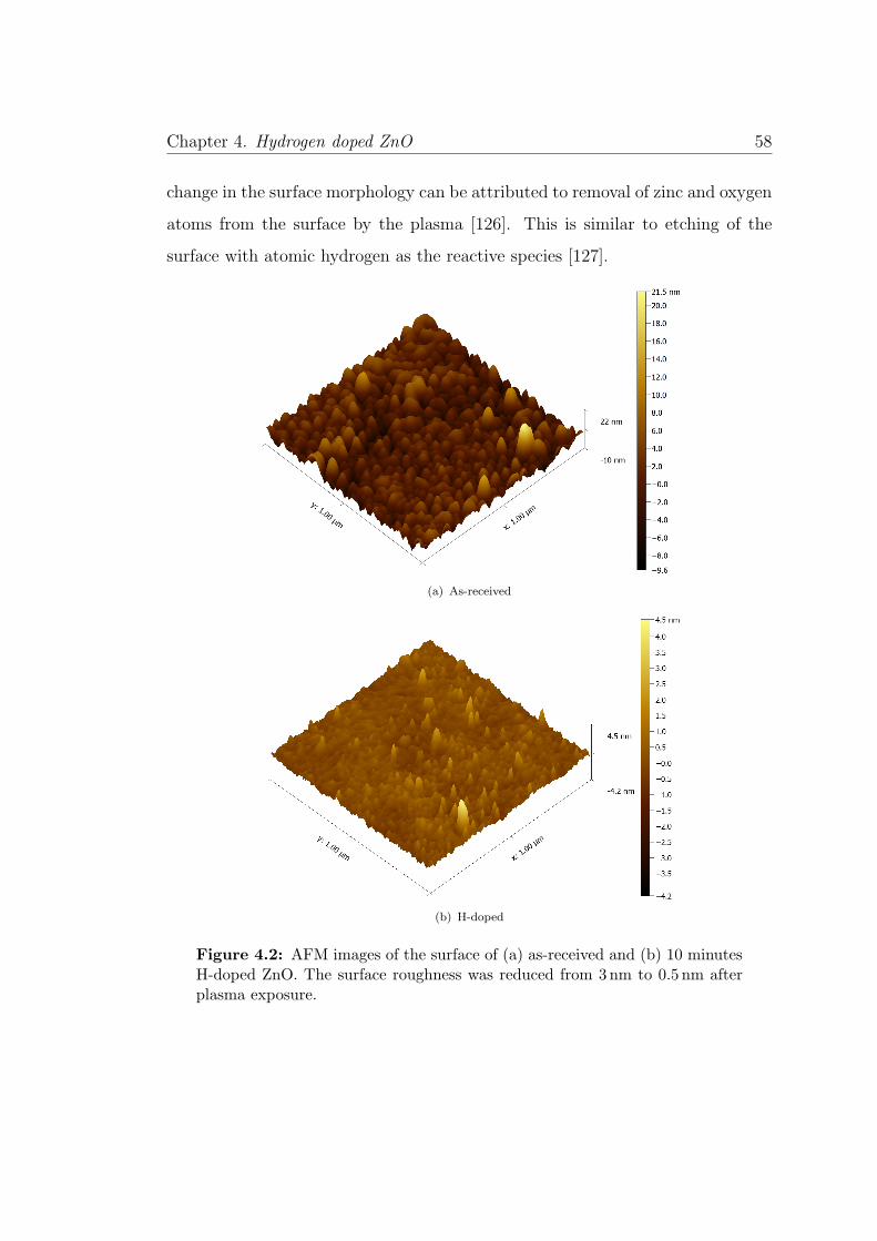
Chapter 4. Hydrogen doped ZnO 58
change in the surface morphology can be attributed to removal of zinc and oxygen
atoms from the surface by the plasma [126]. This is similar to etching of the
surface with atomic hydrogen as the reactive species [127].
(a) As-received
(b) H-doped
Figure 4.2: AFM images of the surface of (a) as-received and (b) 10 minutesH-doped ZnO. The surface roughness was reduced from 3nm to 0.5 nm afterplasma exposure.
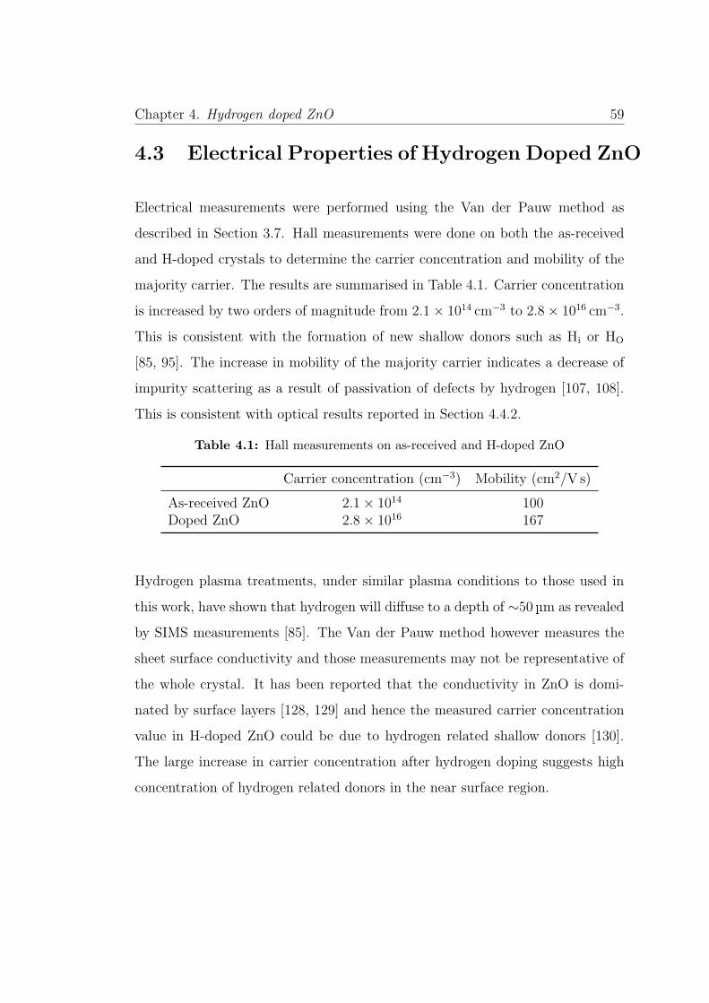
Chapter 4. Hydrogen doped ZnO 59
4.3 Electrical Properties of Hydrogen Doped ZnO
Electrical measurements were performed using the Van der Pauw method as
described in Section 3.7. Hall measurements were done on both the as-received
and H-doped crystals to determine the carrier concentration and mobility of the
majority carrier. The results are summarised in Table 4.1. Carrier concentration
is increased by two orders of magnitude from 2.1× 1014 cm−3 to 2.8× 1016 cm−3.
This is consistent with the formation of new shallow donors such as Hi or HO
[85, 95]. The increase in mobility of the majority carrier indicates a decrease of
impurity scattering as a result of passivation of defects by hydrogen [107, 108].
This is consistent with optical results reported in Section 4.4.2.
Table 4.1: Hall measurements on as-received and H-doped ZnO
Carrier concentration (cm−3) Mobility (cm2/V s)
As-received ZnO 2.1× 10¹⁴ 100Doped ZnO 2.8× 10¹⁶ 167
Hydrogen plasma treatments, under similar plasma conditions to those used in
this work, have shown that hydrogen will diffuse to a depth of ∼50 �m as revealed
by SIMS measurements [85]. The Van der Pauw method however measures the
sheet surface conductivity and those measurements may not be representative of
the whole crystal. It has been reported that the conductivity in ZnO is domi-
nated by surface layers [128, 129] and hence the measured carrier concentration
value in H-doped ZnO could be due to hydrogen related shallow donors [130].
The large increase in carrier concentration after hydrogen doping suggests high
concentration of hydrogen related donors in the near surface region.

Chapter 4. Hydrogen doped ZnO 60
4.4 Optical Properties of Hydrogen doped ZnO
1.5 2.0 2.5 3.10 3.15 3.20 3.25 3.30 3.35 3.40 3.45
I1/2FX-3LO FX-2LO FX-1LO I
4I6
CL
Inte
nsity
(a.u
.)
Energy (eV)
FX
DLE
Figure 4.3: CL spectrum of as-received ZnO showing the FX, BX, FX-1LO,FX-2LO, FX-3LO and the broad deep level emission centered at 2.3 eV. Notethe different scale on the energy axis between the NBE and DLE regions. Thisspectrum was collected at 80K with beam energy of 5 keV and beam currentof 15 nA taken at 80K.
Figure 4.3 shows the CL spectrum from the as-received a-plane ZnO crystal
from MTI Corporation collected at 80K with beam energy of 5 keV and beam
current of 15 nA. This beam energy of 5 keV corresponds to an excitation depth
of ∼100 nm in ZnO. This interaction volume is comparable to the sampling depth
in PL measurements.
The spectrum consists of two distinct luminescence regions; the near band edge
(NBE) in the UV region and a broad deep level emission (DLE) in the visible. The
NBE emission is made up of a series of peaks in the region from 3.15 eV to 3.40 eV.

Chapter 4. Hydrogen doped ZnO 61
The weak shoulder at 3.39 eV is attributed to free exciton (FX) recombinations.
A series of peaks in the region from 3.35 eV to 3.38 eV are attributed to radiative
recombination of excitons bound to shallow donors (D0X or D+X). The main
features in this region are the I6 peak at 3.359 eV, the I1/2 at 3.373 eV and a
shoulder at 3.363 eV which is attributed to the I4. Three additional peaks on
the low energy side of the bound exciton (BX) labeled FX-1LO, FX-2LO and
FX-3LO are also observed. The separation of these peaks is consistent with the
longitudinal optical (LO) phonon mode in ZnO of 72meV [131, 132], so these
peaks are attributed to the first three phonon replica of the free exciton emission.
The CL emission of the crystal also shows a broad deep-level luminescence peak-
ing at 2.35 eV. This peak is often called the deep level emission (DLE). The
origin of this DLE peak is controversial but is often attributed to radiative re-
combination of electron-hole pairs at native defect sites such as VO and VZn or
impurities such as copper [49, 102]. Experimental evidence shows that copper
impurities result in a fine structure within photoluminescence spectra at liquid
helium temperature. The transition from (Cu+,h) to the Cu2+ T2 state results
in a photon with the zero-phonon line of the emission at 2.86 eV [61]. Figure 4.4
shows the CL spectrum of the as-received ZnO taken at 10K. The structureless
profile of the DLE in the a-plane MTI crystals at 10K suggests that the emission
is not due to copper impurities, but originates from native defects [133]. The
broad profile of the DLE when compared to the NBE emission can be explained
in terms of the high coupling of the emission to lattice vibrations [134]. This leads
to peak broadening through phonon emissions. The defect emission is broad and
centred at 2.35 eV. The broad profile of the defect emission and the multitude of
emissions in the DLE region make assignment of individual contributions difficult.

Chapter 4. Hydrogen doped ZnO 62
1.4 1.6 1.8 2.0 2.2 2.4 2.6 2.8 3.0 3.2 3.4 3.6
1.6 2.0 2.4 2.8
CL
Inte
nsity
(a.u
.)
Energy (ev)
Energy (ev)
Figure 4.4: CL spectrum of as-received ZnO at 10K. Inset shows a magnifiedview of the structureless DLE. Collected with beam energy of 5 keV and beamcurrent of 15 nA.
4.4.1 Effects of Hydrogen on the NBE luminescence
Figure 4.5 shows the CL spectra of both the as-received and H-doped crystals after
2 minutes plasma treatment. It is clear that hydrogen doping has a significant
effect on the CL of ZnO. The intensity of the NBE emission is doubled following
hydrogen incorporation. A broadening of the bound exciton emission peaks is
also observed. However, the spectral resolution of the CL system did not allow
for proper investigation of the effects of hydrogen on individual peaks in the NBE
region.
There are three possible mechanisms by which the NBE intensity can increase
after hydrogen treatment:
1. formation of new shallow donor levels, e.g. Hi, which provide additional
efficient radiative recombination channels through the I4 channel.

Chapter 4. Hydrogen doped ZnO 63
1.5 2.0 2.5 3.10 3.15 3.20 3.25 3.30 3.35 3.40 3.45
As-receivedH-Doped
I1/2FX-3LO FX-2LO FX-1LO I
4I6
CL
Inte
nsity
(a.u
.)
Energy (eV)
FX
DLE
Figure 4.5: Comparison of the CL spectra of as-received and H-doped ZnOafter 2 minutes H2 plasma. Both spectra were collected at 80K with a beamenergy of 5 keV and beam current of 15 nA.
2. elimination of competitive radiative recombination channels by the forma-
tion of neutral hydrogen complexes with defect centres.
3. formation of other defect related luminescence centres as a result of damage
caused by the hydrogen plasma.
Hall measurements (see Section 4.3) show an increase in carrier concentration by
two orders of magnitude. This indicates either formation of new shallow donor
levels or passivation of defects and charge traps by the introduction of hydrogen,
leading to the increase of the NBE emission and carrier concentration.
In order to investigate the effects hydrogen had on the bound excitons and
phonons, high resolution photoluminescence was performed. Figure 4.6 shows
the low temperature (T = 7K) PL spectra of the NBE region of both the as-
received and H-doped crystals. The inset shows the donor bound exciton region

Chapter 4. Hydrogen doped ZnO 64
3.14 3.16 3.18 3.20 3.22 3.24 3.26 3.28 3.30 3.32 3.34
TES I6
Y0 & Y
1
FX-B 1LO
D0X-1LO
FX-A1LO
TES I6-1LO
D0X-2LO
D0X-3LO
Inte
nsity
(a.u
.)
Energy (eV)
As-received H-Doped
3.350 3.355 3.360 3.365 3.370 3.375
I1/2
Inte
nsity
(a.u
.)
Energy (eV)
I9
I4
I6
I4a,b
Figure 4.6: High resolution PL spectra of the as-received and H-doped ZnOcrystals taken at 7K. The inset shows the donor bound exciton region of thespectra on a logarithmic scale.
where the I lines are found. The main peak in the as-received crystal is the I6
line at 3.616 eV. Also present are the I9 line at 3.357 eV, the I4 at 3.363 eV and
a broad luminescence centred at 3.368 eV. Of particular interest is the I4 line
which is taken as a signature for hydrogen shallow donors in ZnO [27, 89, 95].
The intensity of the I4 line is increased following hydrogen incorporation and a
slight blue shift of the main peak is observed. For H-doped ZnO, the dominant
peak at 3.362 eV (labelled I4a,b) has previously been attributed to an excited
state of the H-related neutral donor bound exciton I4 [135]. Analysis of the BX
spectral region reveals that the I4a,b intensity increases in comparison with that
of I4 after hydrogen incorporation suggesting that hydrogen dopants introduced
by the plasma are in a different chemical state to those incorporated during the
hydrothermal growth. This is consistent with the CL results and can be inter-
preted as hydrogen forming new shallow donors which act as efficient radiative

Chapter 4. Hydrogen doped ZnO 65
recombination pathways. The broad luminescence at 3.368 eV, which is where
the I2 or I1 lines are expected to be, has also been attributed to an emission
from the “bottleneck” region of the lower polariton branch of the A valence band
(LPBA) [131]. This assignment is unlikely as the intensity of that emission is
expected to increase with carrier concentration. It can be seen that the emission
is quenched following hydrogen doping. It has also been reported that the I2
at 3.368 eV appears in ZnO following lithium doping and has been attributed to
lithium interstitial (Lii) shallow donors [27, 136]. This Lii can then be passivated
by hydrogen, leading to the quenching of the luminescence.
The intensity of the phonon replica of the D0X emission at 3.2903 eV and 3.2180 eV
as well as that of the two-electron satellite (TES) of the I6 at 3.2527 eV are re-
duced after hydrogen incorporation. Conversely, the peak at 3.3363 eV is en-
hanced after hydrogen incorporation. This peak is at the position where the Y0
and Y1 lines are to be expected. The origin of the Y lines is still controversial, but
has recently been attributed to the radiative recombination of excitons bound to
extended structural defects [137]. Such defects could have been created in the
crystal when exposed to the hydrogen plasma.
4.4.2 Effects of Hydrogen on the DLE
In addition to an increase in the NBE emission, hydrogen doping also affects the
DLE as observed in Figure 4.5. The intensity of the DLE peak is reduced and
is separated into two components: one yellow luminescence centered at ∼1.9 eV[50] which is associated to a donor-acceptor pair recombination involving a deep
lithium acceptor occupying a Zn site (LiZn) and a green luminescence centered
at ∼2.35 eV whose origin has been attributed to bulk zinc vacancies (VZn) [39]
or surface oxygen vacancies (VO) [40]. Zinc vacancies are double acceptors and
occur in the 2- charge state (V2−Zn ). Hydrogen, known to act almost exclusively as
positive charge state (H+) [86], would preferentially interact with V2−Zn rather than
Chapter 4. Hydrogen doped ZnO 66
V+O or V++
O centres. This assignment is in agreement with first principle calcula-
tions which predict the existence of a complex involving V2−Zn and two hydrogen
atoms [99]. These VZn-H2 inhibit the involvement of VZn in radiative recombi-
nation, thereby quenching the green luminescence. The increase in the intensity
of the yellow luminescence can be attributed to the quenching of the green lumi-
nescence. As there are a finite number of electron-hole pairs being generated at
any given time, recombination preference is given to the most efficient channel
[138]. By quenching the green luminescence radiative pathway, the probability
of a radiative recombination occurring through the yellow luminescence pathway
increases.
4.4.3 Effects of Temperature on Hydrogen Incorporation
The temperature at which the sample is kept during hydrogen plasma treatment
has significant effects on the optical properties of the crystals near-surface region
as shown in Figure 4.7. The spectra were taken at 80K with a beam energy of
5 keV which corresponds to a CL generation depth of 100 nm and a beam current
of 15 nA. The as-received crystal shows well defined bound exciton peaks and a
broad deep level luminescence centered at 2.31 eV (see beginning of Section 4.4
for a discussion on the peaks).
After hydrogen doping at 25 ◦C, the intensity of the NBE emission is doubled as
seen in Figure 4.7. A broadening of the emission peaks is also observed. This
broadening suggests that damage to the surface is caused by the hydrogen plasma
through sputtering of the surface atoms. An enhancement of the emission at
3.333 eV is observed after hydrogen doping. That spectral position corresponds
to a Y line as shown in the PL measurements before. The DLE was red-shifted
from 2.32 eV to 1.97 eV after hydrogen doping. This apparent shift in the peak
position is due to the quenching of the GL by hydrogen which forms neutral
VZn-H2 complexes that passivate the native VZn which are responsible for the

Chapter 4. Hydrogen doped ZnO 67
1.5 2.0 2.5 3.05 3.10 3.15 3.20 3.25 3.30 3.35 3.40 3.45
I1/2FX-3LO FX-2LO FX-1LO I
4I6
CL
Inte
nsity
(a.u
.)
Energy (eV)
As-receivedDoped 25 °CDoped 200 °CDoped 435 °C
FX
Figure 4.7: CL spectra of as-received and H-doped ZnO crystals with thedoping procedure performed at various temperatures. The plasma exposuretime was kept at 120 s for the doped crystals. All spectra were collected at80K with beam energy of 5 keV and beam current of 15 nA.
GL. The quenching of the GL implies that hydrogen has enough thermal energy
at 25 ◦C to diffuse in the crystal to form a VZn-H2 complex which requires two
hydrogen sitting at the zinc vacancy site. It is accepted that the YL in ZnO is
caused by a radiative recombination of a donor-acceptor pair involving a shallow
donor and a LiZn acceptor. The relative increase in the YL after hydrogen incor-
poration can be explained in terms of competition for carriers in CL. When the
GL pathway was quenched, the probability of a radiative recombination via the
channels responsible for the YL increased. Another possibility is that hydrogen
incorporation increases the donor concentration in the vicinity of LiZn centres,
thereby making the DAP luminescence pathway more efficient.

Chapter 4. Hydrogen doped ZnO 68
3.340 3.345 3.350 3.355 3.360 3.365 3.370 3.375 3.380
As-receivedDoped 25 °CDoped 200 °CDoped 435 °C
Nor
mal
ised
CL
Inte
nsity
(a.u
.)
Energy (eV)
I63.359 eV
I43.364 eV
I1/2
3.373 eV
Figure 4.8: Normalised CL spectra of the bound exciton region. Spectrawere normalised to the I9 line. All spectra were collected at 80K with beamenergy of 5 keV and beam current of 15 nA.
For doping performed at 200 ◦C, the intensity of the NBE emission is increased
compared to the as-received crystal, but is lower than when doping was performed
at 25 ◦C as shown in Figure 4.7. The emission peaks are also narrower and more
defined. The narrowing of the line width is synonymous with an improved crystal
quality caused by the higher temperature of the crystal during hydrogen incor-
poration. This is in effect a low temperature annealing of the crystal. Further
support for this explanation is the decrease of the Y line emission at 3.333 eV.
The overall intensity of the NBE emission being reduced when compared to the
plasma treatment done at 25 ◦C as in Figure 4.8 can be caused by two factors: (1)
hydrogen diffusing from the near-surface layer deep into the bulk or (2) hydrogen
being removed from the surface at the higher temperature. Previous reports have
found that hydrogen is stable in ZnO at temperatures of up to ∼500 ◦C [85, 95].

Chapter 4. Hydrogen doped ZnO 69
The lower temperature involved in this case would imply diffusion of hydrogen
deeper in the bulk. This also explains the decrease of the NBE intensity when
compared to the sample at 25 ◦C. Similar to the 25 ◦C case, the GL was decreased.
However, the effect was less significant. Hydrogen has higher thermal energy at
200 ◦C than at 25 ◦C and hence can travel deeper in the bulk before interacting
with native defects such as VZn.
At 400 ◦C the crystal seems to be more damaged by the hydrogen plasma. At
such high temperatures, it is expected that sputtering of the surface Zn or O
atoms by hydrogen species takes place more easily. This damage can be seen in
Figure 4.7 as a broad luminescence centered at ∼3.15 eV and a decrease in the
NBE intensity when compared to the as-received crystal. The intensity of the
GL has not changed when compared to the as-received sample while that of the
YL was slightly increased.
While low voltage CL gives information of the crystals near surface regions, it
is necessary to perform depth dependent CL to have a better idea of hydrogen
incorporation and diffusion. The DLE is also made up of two distinct emissions,
the green and the yellow emission. It is therefore necessary to deconvolve the
broad peak centered at 2.31 eV into two components for proper analysis.
4.4.4 Deconvolution of the Deep-Level Luminescence Band
The DLE peak in ZnO consists of at least two distinct emissions (Figure 4.5).
One in the green region attributed to VZn and a yellow component attributed to
LiZn. In order to investigate these components and find fit parameters, an as-
received ZnO crystal was doped with lithium. A 50 nm layer of lithium metal was
thermally evaporated on a clean a-plane ZnO crystal surface in a vacuum. The
coated crystal was then annealed in-situ in the deposition chamber for 30min at
950 ◦C to indiffuse lithium acceptors in the crystal. Figure 4.9 shows the XPS

Chapter 4. Hydrogen doped ZnO 70
spectra of the Li 1s core level for both the as-received and Li doped crystals
taken at an X-ray photon energy of 160 eV. A peak at binding energy of 54.7 eV
appears in the Li doped crystal. This indicates that Li has been incorporated in
the ZnO crystals.
59 58 57 56 55 54 53 52 51 50
XP
SIn
tens
ity(a
.u.)
Binding Energy (eV)
Li dopedAs-received
Li 1s
Figure 4.9: XPS spectra of the Li 1s core level for the as-received and Lidoped crystals taken at a photon energy of 160 eV.
Figure 4.10 shows the CL spectrum of the yellow emission in the Li doped ZnO
crystal taken at 80K. The Li-doped ZnO displays deep level emission dominated
by the yellow luminescence. The yellow luminescence in ZnO is known to couple
strongly with phonons in the lattice and it has been reported to have a Huang-
Rhys factor of S = 13 [139]. This large Huang-Rhys factor indicates that the peak
is symmetrical and can therefore be fit with a single Gaussian function [134]. A
least square Gaussian fit of the yellow luminescence resulted in a peak centered
at 1.95 eV with a full width at half maximum (FWHM) of 0.58 eV.
Tying down the peak energy and FWHM parameters for the yellow luminescence
and letting the green luminescence fit accordingly means that a unique fit is
achieved every time. Figure 4.11 shows such a deconvolution with two Gaussian

Chapter 4. Hydrogen doped ZnO 71
1.2 1.4 1.6 1.8 2.0 2.2 2.4 2.6 2.8
CL
Inte
nsity
(a.u
.)
Energy (eV)
Experimental dataGaussian fit
0.58 eV
1.95 eV
Figure 4.10: CL spectrum of the Li doped crystal showing the least squareGaussian fit of emission. Peak position at 1.95 eV and FWHM of 0.58 eV.Spectrum was collected at 80K with beam energy of 15 keV and beam currentof 4 nA
components and a fit to the DLE achieved by a non-linear least square fitting
algorithm. This fit yielded the parameters for the GL of peak position at 2.35 eV
and FWHM of 0.51 eV.
The fit parameters for the yellow and green luminescences used in this project
are summarised in Table 4.2. When comparing the contribution of different
emission in depth or power resolved experiments, the integrated intensity of the
deconvolved peaks were used instead of peak height. For the NBE emission, the
whole integrated intensity of the region from 3 eV to 3.4 eV was used.
Table 4.2: Fit parameters for the yellow and green luminescences obtainedby least square Gaussian fits
Peak Peak Position FWHM
Yellow luminescence 1.95 eV 0.58 eVGreen luminescence 2.35 eV 0.51 eV

Chapter 4. Hydrogen doped ZnO 72
1.2 1.4 1.6 1.8 2.0 2.2 2.4 2.6 2.8 3.0
CL
Inte
nsity
(a.u
.)
Energy (eV)
Experimental dataGreenYellowFit
Figure 4.11: The DLE peak of ZnO has been deconvolved into two Gaussiancomponents. The yellow component at 1.95 eV with FWHM of 0.58 eV andthe green component at 2.35 eV with FWHM of 0.51 eV.
4.4.5 Depth Distribution of Luminescence Centres
As the energy of the beam determines the penetration depth of electrons, and
consequently the depth at which CL is generated, it is possible to control the
depth at which CL is generated. The number of electron-hole pairs generated
is proportional to the beam power and can be approximated by the following
equation [138]:
[n]eh ∝ Ib · Eb (4.1)
where [n]eh is the number of electron-hole pairs generated, Ib is the beam current
and Eb is the beam energy. By varying both the beam current and beam energy
to keep the power constant, it is possible to obtain information on the depth
distributions of a luminescence centre such as a defect. For example, if CL is
collected at low beam energies, information about the surface is collected, while

Chapter 4. Hydrogen doped ZnO 73
increasing the beam energy gives more information about the bulk properties of
the sample.
One limitation of this technique is the higher energy tail of band-edge lumines-
cence from semiconductors can be readily re-absorbed by the material itself, lead-
ing to an apparent red-shift. The emitted light intensity follows a Beer-Lambert
relation [140]:
I = I0 exp(−αd) (4.2)
where α is the absorption coefficient and d is the photon generation depth. This
self-absorption effect is more pronounced when high beam energies are used i.e.
photons are generated at depths of several micrometres below the surface.
4.4.5.1 Simulations of CL Interaction Volumes in ZnO
The penetration depth and consequently the interaction volume of an electron
beam depends on the beam energy. In order to correlate the beam energy to CL
generation depth, the CASINO package [111] was used for Monte Carlo simula-
tions of the electron beam interaction with ZnO material.
Figure 4.12 shows the typical shape of the energy loss profile of electrons in
ZnO as obtained from the CASINO simulations. The energy loss curve data
was obtained from CASINO simulations using the parameters in Table 3.2. At
low accelerating voltages most of the energy is dissipated within a small volume.
At higher beam energies the tail of the energy loss curve decays deep into the
sample. As a result, maximum penetration depths give a poor indication of CL
generation. Simulations have been done for the primary beam energy range of
0.1 keV to 30 keV. It is generally accepted that the CL generation depth is taken
as the depth at which 75% of the energy is dissipated under the energy loss
profile. Figure 4.13 shows the CL generation depth which has been calculated by
integrating over the simulated energy loss curves.

Chapter 4. Hydrogen doped ZnO 74
0 500 1000 1500 2000 2500 3000 3500 40000.0
0.5
1.0
1.5
2.0
2.5
3.0
3.5C
LIn
tens
ity(%
)
Depth (nm)
5 keV10 keV15 keV20 keV25 keV30 keV
Figure 4.12: CASINO simulated electron energy loss curves for beam en-ergies of 5 keV, 10 keV, 15 keV, 20 keV, 25 keV and 30 keV. The vertical axiscorresponds to the percentage of CL generated at that particular depth.
0 5 10 15 20 25 300
250
500
750
1000
1250
1500
CL
Gen
erat
ion
dept
h(n
m)
Beam Energy (keV)
Figure 4.13: CL generation depth as a function of electron beam energy.The depth here corresponds to the depth at which 75% of the electron beamenergy has been lost.

Chapter 4. Hydrogen doped ZnO 75
4.4.5.2 Distribution of Luminescence Centres in H-doped ZnO
Depth-resolved cathodoluminescence (DRCL) was used to determine the spatial
distribution of luminescence centres from the surface of the crystal. By correlating
electron beam energies to electron interaction volumes obtained from CASINO
simulations (Section 4.4.5.1), it is possible to estimate the depth at which the CL
signal is generated. In DRCL, the beam power is kept constant by varying both
the beam energy and current at the same time. It is therefore expected that the
number of electron-hole pairs generated in each scan to be constant. In this ideal
case with a homogeneous distribution of luminescence centres throughout the
depth of the sample and neglecting surface recombinations, a flat horizontal line
with constant intensity, which represents the integrated area of the luminescence
peaks, is expected.
Figure 4.14 shows the DRCL spectra for the as-received and H-doped crystals
where doping was performed at 25, 200 and 435 ◦C. The DRCL spectra represent
the integrated area under the respective CL spectra for each luminescence band.
The beam power was kept constant at 30 �W throughout all acquired scans. In all
samples, for beam energies of Eb < 2 keV, which corresponds to a layer of about
30 nm, no CL emission was observed. This is due to non-radiative defects caused
by surface polishing damage completely quenching any luminescence [141]. For
the as-received ZnO sample, the NBE emission rapidly increases after the first
2 keV to reach a maximum at a depth of 170 nm. With higher beam energies,
the NBE emission is constant and does not show any self-absorption effects (See
Equation 4.2). This shows that DRCL is a valid technique to use for the study
of light emission from different depths of a sample.
The NBE luminescence of the ZnO crystals is significantly changed after hydrogen
incorporation. For the sample doped at 25 ◦C, the maximum NBE intensity was
increased by one order of magnitude when compared to the as-received sample
as in Figure 4.14 (a). The NBE intensity rises quickly from 2 keV to peak at

Chapter 4. Hydrogen doped ZnO 76
0 67 180 340 546 798 1097 1442
CL Generation Depth (nm)
(a) NBE
As-receivedDoped 25 °CDoped 200 °CDoped 435 °C
CL
Inte
nsity
(a.u
)
(b) Yellow Luminescence
0 2 4 6 8 10 12 14 16 18 20 22 24 26 28 30Beam Energy (keV)
(c) Green Luminescence
Figure 4.14: Distribution of luminescence centres in as-received ZnO andH-doped ZnO crystals at different temperatures. Integrated intensity for (a)NBE emission, (b) yellow luminescence and (c) green luminescence are shownfrom 2 keV to 30 keV. Spectra were collected at 80K with a beam power of30 �W. The top x-axis is the CL generation depth in ZnO corresponding to75% CL intensity obtained by CASINO simulations.

Chapter 4. Hydrogen doped ZnO 77
10 keV which corresponds to a CL generation depth of ∼250 nm and then drops
for higher beam energies. The enhancement of the NBE is consistent with the
formation or new Hi shallow donors in the near surface region. In fact, the depth
profile of the NBE luminescence can be used to approximate the distribution of
hydrogen donors incorporated in the crystal by the plasma treatment.
Hydrogen doping (Figure 4.14 (c)) causes the GL to be quenched in the top
500 nm of the crystal. The intensity of the GL then increases until it reaches
the same profile as the as-received crystal at 900 nm depth. The discrepancy
between the NBE and GL profile is due to the fact that hydrogen is more likely
to stay as single Hi than interact with native defects to form VZn-H2 complexes,
specially when the concentration of Hi is low which is the case at depths below
900 nm. The reduction in the green intensity is fairly constant within the depth
range 30 nm to 800 nm, indicating a uniform hydrogen concentration, in good
agreement with other types of depth profiling measurements [123]. The fact that
the green luminescence is quenched at depths reaching several �m in the bulk
demonstrates that surface oxygen vacancies cannot be the source of the green
luminescence but that they most likely originate from bulk zinc vacancies. The
YL is enhanced throughout the whole sampling range because of the quenching
of the GL.
Increasing the temperature at which the ZnO crystal was kept at during hydro-
gen incorporation from 25 ◦C to 200 ◦C increases the diffusion of hydrogen deeper
in the bulk. In Figure 4.14 (a), it can be seen that the peak of NBE lumi-
nescence occurs at 1000 nm, increasing from 250 nm when the temperature was
increased. This is consistent with hydrogen species having higher thermal energy
(from 25meV to 42meV) and can therefore diffuse deeper in the bulk. This be-
haviour can also be seen in the GL depth profile from Figure 4.14 (c). The GL
is still quenched in the near surface region, but at depths deeper than 900 nm
the intensity of the GL in the H-doped crystal is still lower than the as-received.

Chapter 4. Hydrogen doped ZnO 78
This is in contrast to when hydrogen doping was performed at 25 ◦C. The profile
shows that hydrogen has indeed diffused deeper at 200 ◦C than at 25 ◦C.
For the crystal doped at 435 ◦C, the apparent increase of the NBE luminescence
when compared to the as-received crystal is not due to hydrogen but caused by
the formation of the new band at 3.15 eV as shown in Figure 4.7. The profile of
the NBE also suggests that no hydrogen has been incorporated in the form of Hi
donors. It is possible that the higher temperature of 435 ◦C is more favourable
for the removal of hydrogen from the crystal than its incorporation. The depth
profiles of both the YL and GL follow the as-received crystal in the near sur-
face region, but increase with depths below 200 nm. The fact that the GL does
not show any quenching effects means that VZn-H2 complexes were not formed
because hydrogen was not incorporated in the crystal at that temperature.
4.4.6 Effect of Plasma Exposure Time on the Lumines-
cence
To optimise the emission efficiency of the crystals through hydrogen doping, the
CL intensity was monitored as a function of plasma exposure time with the
sample kept at 25 ◦C. The deconvolved CL emission from the NBE, yellow and
green emissions are shown in Figure 4.15. The NBE intensity increases by about
one order of magnitude after 120 s then shows a decrease in intensity with further
plasma exposure. This decrease could be due to damage in the crystal caused
by removal of atoms from the surface of the crystal [126, 127]. Another possible
explanation is the formation of hydrogen molecules (H2) at high concentration
of Hi [90, 142]. H2 being a neutral impurity, does not take part in radiative
recombination and hence leads to a decrease in the D0X emission.
The intensity of the green luminescence is halved after 120 s. The emission is
not quenched entirely because the depth of the interaction volume is bigger than
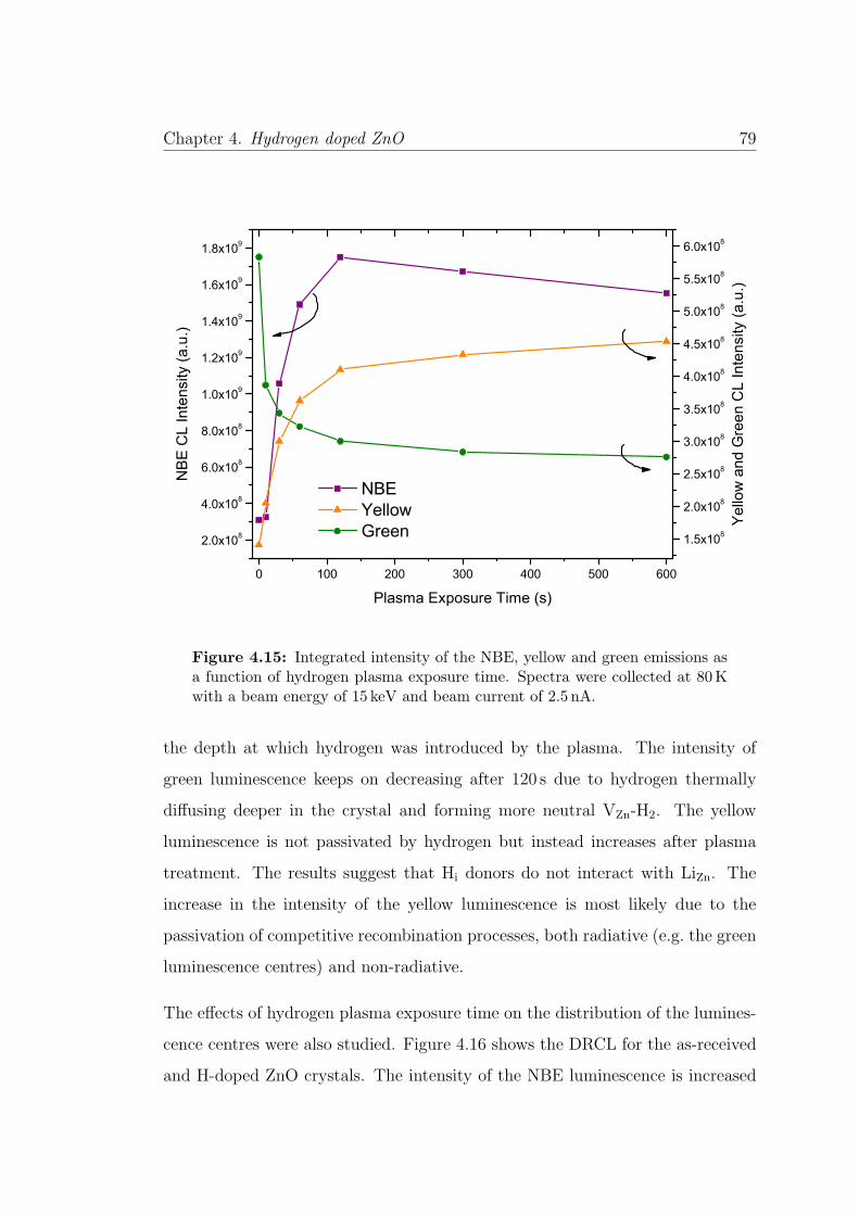
Chapter 4. Hydrogen doped ZnO 79
0 100 200 300 400 500 600
2.0x10⁸
4.0x10⁸
6.0x10⁸
8.0x10⁸
1.0x10⁹
1.2x10⁹
1.4x10⁹
1.6x10⁹
1.8x10⁹
NBE Yellow Green
Plasma Exposure Time (s)
NB
E C
L In
tens
ity (a
.u.)
1.5x10⁸
2.0x10⁸
2.5x10⁸
3.0x10⁸
3.5x10⁸
4.0x10⁸
4.5x10⁸
5.0x10⁸
5.5x10⁸
6.0x10⁸
Yel
low
and
Gre
en C
L In
tens
ity (a
.u.)
Figure 4.15: Integrated intensity of the NBE, yellow and green emissions asa function of hydrogen plasma exposure time. Spectra were collected at 80Kwith a beam energy of 15 keV and beam current of 2.5 nA.
the depth at which hydrogen was introduced by the plasma. The intensity of
green luminescence keeps on decreasing after 120 s due to hydrogen thermally
diffusing deeper in the crystal and forming more neutral VZn-H2. The yellow
luminescence is not passivated by hydrogen but instead increases after plasma
treatment. The results suggest that Hi donors do not interact with LiZn. The
increase in the intensity of the yellow luminescence is most likely due to the
passivation of competitive recombination processes, both radiative (e.g. the green
luminescence centres) and non-radiative.
The effects of hydrogen plasma exposure time on the distribution of the lumines-
cence centres were also studied. Figure 4.16 shows the DRCL for the as-received
and H-doped ZnO crystals. The intensity of the NBE luminescence is increased

Chapter 4. Hydrogen doped ZnO 80
0 67 180 340 546 798 1097 1442
0 2 4 6 8 10 12 14 16 18 20 22 24 26 28 30
CL Generation Depth (nm)C
LIn
tens
ity(a
.u.)
0 s10 s30 s60 s
(a) NBE
(b) Yellow Luminescence
CL
Inte
nsity
(a.u
.)
(c) Green Luminescence
CL
Inte
nsity
(a.u
.)
Beam Energy (keV)
Figure 4.16: Distribution of luminescence centres in ZnO crystals for (a)NBE (b) yellow and (c) green luminescences as a function of hydrogen plasmatime. Spectra were collected at 80K with a beam power of 30 �W. The topx-axis is the CL generation depth in ZnO corresponding to 75% CL intensityobtained by CASINO simulations.

Chapter 4. Hydrogen doped ZnO 81
with increasing plasma time. The overall trend of the depth profiles do not change
with increasing plasma exposure. Only the intensity is increased. The plasma
exposure time dependent green luminescence profiles (Figure 4.16 (c)) show that
this luminescence is being quenched after only 10 s of plasma exposure.
This indicates that hydrogen is incorporated at depths up to 350 nm in less than
10 s. With increasing plasma time, the shape of the depth profiles do not change,
but the effects of the hydrogen plasma are enhanced. While the surface green
luminescence is already mostly quenched in the first 10 s, the intensity of the
luminescence keeps on decreasing further in the bulk with plasma time, indi-
cating thermal diffusion of hydrogen deeper in the bulk. This is in agreement
with first principle calculations which predict hydrogen to be mobile in ZnO at
temperatures as low as 100 ◦C [106].
4.5 Raman Spectroscopy
Raman spectroscopy was used in this project to investigate any effects that hy-
drogen could have on the vibrational modes of ZnO. This can be in the forms of
formation of new Raman peaks attributed to hydrogen forming bonds with ZnO
or forming H2 molecules. Other spectral changes could be shifts or quenching of
native ZnO peaks.
ZnO exists mainly in the hexagonal wurtzite structure with four atoms per unit
cell and belongs to the C46v(P63mc) space group. From the group theory, one will
theoretically expect one A1, one E1, two E2, and two B1 optical phonon modes
[116, 144]. Phonon modes of A1, E1 and E2 symmetry are Raman active while the
B1 mode is silent. The polar characteristics of the A1 and E1 vibrational modes
give rise to both longitudinal and transverse components. A typical Raman
spectrum of the as-received a-plane ZnO crystal is shown in Figure 4.17. Peaks
at 205, 332, 378, 438, 540, 584, 615, 670 and 724 cm−1 were clearly observed
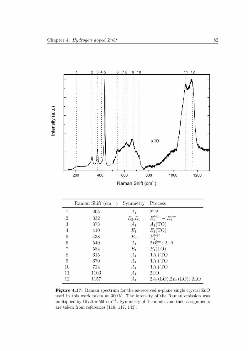
Chapter 4. Hydrogen doped ZnO 82
200 400 600 800 1000 1200
108 121196 7543
Inte
nsity
(a.u
.)
Raman Shift (cm-1)
21
x10
Raman Shift (cm−1) Symmetry Process
1 205 A1 2TA
2 332 E2,E1 Ehigh2 − E low
2
3 378 A1 A1(TO)4 410 E1 E1(TO)
5 438 E2 Ehigh2
6 540 A1 2Blow1 ; 2LA
7 584 E1 E1(LO)8 615 A1 TA+TO9 670 A1 TA+TO10 724 A1 TA+TO11 1103 A1 2LO12 1157 A1 2A1(LO),2E1(LO); 2LO
Figure 4.17: Raman spectrum for the as-received a-plane single crystal ZnOused in this work taken at 300K. The intensity of the Raman emission wasmultiplied by 10 after 500 cm−1. Symmetry of the modes and their assignmentsare taken from references [116, 117, 143].

Chapter 4. Hydrogen doped ZnO 83
in the low frequency region. Moreover, there is a very weak shoulder located
at the low energy side of the 438 cm−1 peak, which corresponds to the E1(TO)
at 410 cm−1. Further peaks located at 1103 and 1157 cm−1 were also found in
the high frequency regions. No more high-order peaks could be observed at
frequencies over 1200 cm−1. The E2 peak at 438 cm−1, being the main peak in
the Raman spectrum, suggests good crystal quality [145, 146]. The peaks in
the Raman spectra along with their corresponding symmetries and processes are
summarised in Figure 4.17.
Raman spectroscopy was performed on both the as-received and hydrogen doped
crystals. Figure 4.18 shows the Raman spectra for both the as-received and
H-doped ZnO crystals. The H-doped crystal shows the same peaks as the as-
received one. No peak shifts or additional peaks were found, indicating no changes
in the crystal quality. It is worth noting that ZnO is transparent to red light
(λ = 633 nm) and hence most of the Raman signal comes from the bulk of the
material and any surface damage from sputtering of Zn or O atoms from the
surface of the crystal would not be clearly seen in the Raman spectra. The
intensity of the E2 peak in both the as-received and H-doped crystals is similar
and indicates that hydrogen doping has not degraded the bulk crystal quality.
This suggests that any damage done by the hydrogen plasma, such as etching
effects (see Section 4.2), is highly localised at the surface of the crystals.
There have been reports of Raman modes associated to hydrogen in ZnO. The
appearance of a mode at 3611 cm−1 after hydrogen plama treament is associated
with the stretch mode of the O−H bond of the interstitial bond-centred hydrogen
[147]. Other modes at 4145, 3628, and 2985 cm−1 are associated with vibrational
modes of interstitial H2, HD and D21 molecules [90]. These modes were however
not detected in this work. The main reasons for this could be the difference
between acquisition conditions and doping conditions. A red laser (λ = 633 nm)
was used to perform the Raman measurements while the Raman modes reported
1D is the deuterium atom which is heavy hydrogen 21H
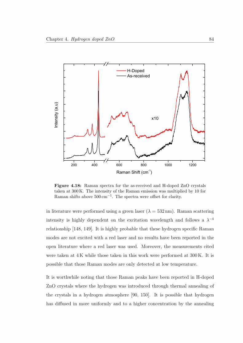
Chapter 4. Hydrogen doped ZnO 84
200 400 600 800 1000 1200
Inte
nsity
(a.u
)
Raman Shift (cm-1)
H-DopedAs-received
x10
Figure 4.18: Raman spectra for the as-received and H-doped ZnO crystalstaken at 300K. The intensity of the Raman emission was multiplied by 10 forRaman shifts above 500 cm−1. The spectra were offset for clarity.
in literature were performed using a green laser (λ = 532 nm). Raman scattering
intensity is highly dependent on the excitation wavelength and follows a λ−4
relationship [148, 149]. It is highly probable that these hydrogen specific Raman
modes are not excited with a red laser and no results have been reported in the
open literature where a red laser was used. Moreover, the measurements cited
were taken at 4K while those taken in this work were performed at 300K. It is
possible that those Raman modes are only detected at low temperature.
It is worthwhile noting that those Raman peaks have been reported in H-doped
ZnO crystals where the hydrogen was introduced through thermal annealing of
the crystals in a hydrogen atmosphere [90, 150]. It is possible that hydrogen
has diffused in more uniformly and to a higher concentration by the annealing

Chapter 4. Hydrogen doped ZnO 85
procedure than through plasma exposure. It was found in Section 4.4.5.2 that
hydrogen diffused to only a few �m from the surface of the crystal exposed to
the plasma. Red light is not absorbed by ZnO and hence can travel through the
whole thickness (500 �m) of the crystal. It is then expected that the majority of
the Raman signal will come from the untreated part of the sample and the layer
that contains hydrogen dopants is too thin to contribute enough Raman signal.
It is also possible that the detector sensitivity at high Raman shifts is too low to
detect anything in that region.
4.6 Synchrotron Light Measurements
Synchrotron light measurement techniques such as X-ray photoelectron spec-
troscopy (XPS) and X-Ray Absorption Near Edge Spectroscopy (XANES) were
used to investigate the chemical states of zinc and oxygen ions before and after
hydrogen doping. XPS was used to study the electronic structure of the ZnO
crystals, namely the charge states and the band structure and election distribu-
tion. XANES was used to study the local structure around Zn and O atoms in
the crystals and how it is affected by hydrogen incorporation.
4.6.1 X-Ray Photoelectron Spectroscopy
X-ray photoelectron spectroscopy (XPS) was used to analyse the chemical states
and valence band of both as-received and H-doped ZnO crystals. Figure 4.19
shows the XPS spectrum of the as-received ZnO taken with photon energy of
1487 eV and the X-ray beam incident at an angle of 55� to the normal of the
surface of the crystal. The characteristic background originates from electrons
that are emitted from ionised atoms deeper under the surface and undergo in-
elastic scattering processes before they leave the surface of the crystal. The 0 eV
level equals the Fermi level of the sample. Several peaks can be observed and it

Chapter 4. Hydrogen doped ZnO 86
1200 1000 800 600 400 200 0
Zn 2p1/2
Inte
nsity
(a.u
.)
Binding Energy (eV)
Zn 2p3/2
Zn 2s
O 1s
C 1sZn 3s
Zn 3p
Zn 3d
Zn LMMO 2s
Figure 4.19: XPS spectrum of the as-received a-plane ZnO crystal used inthis work with core shell zinc and oxygen photoelectron peaks labeled. Theregion marked LMM are the Auger electrons of zinc. The X-ray photon energywas set at 1487 eV.
is important to distinguish which ones are fundamental to the technique, result
from instrumental effects or depend on the chemical nature of the sample and
can provide information on the constituents.
Zinc displays a series of lines in the XPS spectrum with each line originating
from a particular core level. The line at 1195 eV comes from the 2s core shell
of zinc. Two lines at 1045 eV and 1022 eV exhibit the characteristic spin-orbit
splitting of the 2p level with the typical intensity ratio of 1:2 and belong to the
Zn 2p1/2 and Zn 2p3/2 respectively. Further peaks associated with zinc are the
3s level at 140 eV, the 3p3/2 at 89 eV and the 3d peak at a binding energy of
10 eV. Furthermore, several Auger lines associated with zinc can be identified.
These lines occur when an inner core vacancy, that was created by the emission
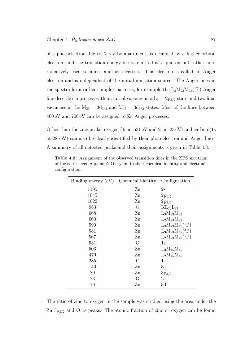
Chapter 4. Hydrogen doped ZnO 87
of a photoelectron due to X-ray bombardment, is occupied by a higher orbital
electron, and the transition energy is not emitted as a photon but rather non-
radiatively used to ionise another electron. This electron is called an Auger
electron and is independent of the initial ionisation source. The Auger lines in
the spectra form rather complex patterns, for example the L3M23M45(1P) Auger
line describes a process with an initial vacancy in a L3 = 2p3/2 state and two final
vacancies in the M23 = 3d3/2 and M45 = 3d5/2 states. Most of the lines between
400 eV and 700 eV can be assigned to Zn Auger processes.
Other than the zinc peaks, oxygen (1s at 531 eV and 2s at 23 eV) and carbon (1s
at 285 eV) can also be clearly identified by their photoelectron and Auger lines.
A summary of all detected peaks and their assignments is given in Table 4.3.
Table 4.3: Assignment of the observed transition lines in the XPS spectrumof the as-received a-plane ZnO crystal to their chemical identity and electronicconfiguration.
Binding energy (eV) Chemical identity Configuration
1195 Zn 2s1045 Zn 2p1/2
1022 Zn 2p3/2
983 O KL23L23
668 Zn L3M23M45
660 Zn L2M23M23
590 Zn L3M23M45(1P)
581 Zn L3M23M45(3P)
567 Zn L2M23M45(1P)
531 O 1s503 Zn L3M45M45
479 Zn L2M45M45
285 C 1s140 Zn 3s89 Zn 3p3/2
23 O 2s10 Zn 3d
The ratio of zinc to oxygen in the sample was studied using the area under the
Zn 3p3/2 and O 1s peaks. The atomic fraction of zinc or oxygen can be found
Chapter 4. Hydrogen doped ZnO 88
using the following equation [151]:
[Zn] =IZn/SZn
IZn/SZn + IO/SO
or [O] =IO/SO
IZn/SZn + IO/SO
(4.3)
where I is the area under the relevant peak and S is the atomic sensitivity factor
(ASF). ASF values are empirically measured for each photoemission peak and are
designed to scale the measured areas so that meaningful atomic concentrations
can be obtained, regardless of the peak chosen. The ASF at a photon energy of
1486.7 eV for zinc 2p3/2 and oxygen 1s are 5.26 and 0.726 respectively [151]. The
ratio of zinc to oxygen in the as-received crystal was found to be 0.47:0.53. This
ratio is within the range of the uncertainty of the XPS quantisation method and
can be considered to be in a 1:1 ratio. It is worth noting that the as-received and
the H-doped crystals all show a 1:1 zinc to oxygen ratio.
Of particular interest in terms of hydrogen doping, the oxygen 1s state was further
investigated because it is very sensitive to chemical environment and these are
reflected in peak shifts or shape changes of the peak. High resolution spectra
(100meV) of the O 1s were recorded at different X-ray photon energies. The
X-ray penetration length in ZnO can be found using the following relation [152]:
δp =1
α(4.4)
where δp is the penetration depth and α is the energy dependent attenuation
depth.
With higher X-ray photon energy, the kinetic energy of the photoelectrons are
higher according to the relation:
Ek = hω − Eb − φ (4.5)
where hω is the energy of the X-ray photon, Eb is the binding energy of the

Chapter 4. Hydrogen doped ZnO 89
electron and φ is the work function. Higher kinetic energy also means that the
probing depth will be higher according to Figure 4.20 which shows the inelastic
mean free path (IMFP) of electrons. The IMFP of an electron is the distance
an electron can travel without undergoing inelastic collisions. The curve shows
that the mean free path is not strongly dependent on the material, but that it
is strongly dependent on the electron energy, with the shortest IMFP of ∼5�A at
50 eV electron energy.
Figure 4.20: Universal curve of the inelastic mean free path of electrons insolids as a function of their energy. From [153].
High resolution XPS spectra of the O 1s core shell were taken at X-ray photon
energies of 650, 750, 850, 1000, 1200 and 1487 eV and are presented in Figure 4.21.
This corresponds to a probing depth range of ∼20�A at a photon energy 650 eV
to ∼60�A at 1487 eV.
It can clearly be seen that the O 1s peak consists of two components. These
two components correspond to oxygen in two different chemical states: the lower
energy component at ∼530.5 eV originates from O2– ions fully coordinated by
zinc ions in the lattice and the higher energy component at ∼532.0 eV being
from hydrogenated O2– ions [23, 154–156].
It was found that the high energy component at 532.0 eV is enhanced after hydro-
gen incorporation at both temperatures when compared to the as-received crystal

Chapter 4. Hydrogen doped ZnO 90
534 532 530 528
(b)
XP
S In
tens
ity (a
.u.)
650 eV 750 eV 850 eV 1000 eV 1200 eV 1487 eV
(a)
534 532 530 528
Binding Energy (eV)
534 532 530 528
(c)
Figure 4.21: High resolution normalised XPS spectra of the O 1s core levelof (a) as-received, (b) H-doped at 25 ◦C and (c) H-doped at 200 ◦C crystalstaken at X-ray photon energies ranging from 650 eV to 1487 eV.
at the same X-ray energies. The crystal doped at 25 ◦C shows more enhancement
of the 532.0 eV component when compared to the one doped at 200 ◦C. The pres-
ence of the higher energy component in the as-received crystal can come from
the unintentional hydrogen doping during hydrothermal growth of the crystal or
from adsorbed surface −OH groups. An enhancement of the higher energy side
is not unexpected because the incorporated hydrogen can lead to the formation
of hydrogenated O2– ions. Calculations predict the VZn-H2 complex to comprise
of two non-equivalent O−H bonds with the hydrogen atoms sitting at the VZn
site. One of the O−H bond is aligned 10� off the c-axis of the crystal while the
second O−H bond is at an angle of 100� to the c-axis [99, 157]. The increase of
the 532.0 eV component is in agreement with CL measurements (see Section 4.4)
Chapter 4. Hydrogen doped ZnO 91
which showed a quenching of the green luminescence after hydrogen incorpo-
ration. The proposed cause for the quenching behaviour was the formation of
neutral VZn-H2 complexes. The 532.0 eV component is also more pronounced
when XPS was collected with an X-ray energy beam of 650 eV than at higher
photon energies. This is consistent with hydrogen diffusion in ZnO being non-
uniform and the diffusion being temperature dependent and is in good agreement
with depth-resolved CL measurements (see Section 4.4.5). The crystal treated
at 25 ◦C shows higher enhancement of the 232.0 eV compared to that at 200 ◦C.
This indicates a higher concentration of hydrogen in the near surface region in the
sample doped at the lower temperature. The hydrogen is able to diffuse deeper
at higher temperatures, thereby reducing its concentration in the near surface
region, as evidenced by the lower intensity of the 532.0 eV component at higher
treatment temperatures.
The valence band (VB) photoelectron spectra were also collected for all three
crystals and are shown in Figure 4.22. The spectra were collected before and
after a 20min argon ion sputtering surface cleaning procedure. The collected
VB spectra were normalised to the Zn 3d peak at 10.2 eV. There are two main
features in the valence band of the crystals: one peak, B, centered at 7.1 eV and
a peak, A, centered at 4.3 eV. Peak B has been assigned to the mixed O 2p and
Zn 4s states while peak A has been assigned to O 2p states [158, 159].
The onset of the valence band for the as-received crystal is shifted from 3.0 eV
to 2.7 eV below the Fermi level after Ar ion sputtering. This is consistent with
adsorbed surface defects, e.g. −OH groups, increasing the n-type conductivity
of the crystal. The intensity of both the A and B peaks of the doped samples
is increased following hydrogen plasma. The valence band onset is also reduced
to ∼1.2 eV when compared to the as-received crystal. After Ar ion sputtering,
the valence band of all three crystals display similar intensities and shapes. This
indicates that surface states were created by the hydrogen plasma for the doped
samples and were removed after Ar ion sputtering. The change in the valence

Chapter 4. Hydrogen doped ZnO 92
9 8 7 6 5 4 3 2 1 0 -1
A
Inte
nsity
(a.u
.)
Binding Energy (eV)
B
(a)
9 8 7 6 5 4 3 2 1 0 -1
A
Binding Energy (eV)
As-receivedH-doped 25 °CH-doped 200 °C
B
(b)
Figure 4.22: Valence-band photoemission spectra of the as-received, H-dopedat 25 ◦C and H-doped at 200 ◦C ZnO crystals. Spectra were taken (a) beforeand (b) after 20 minutes of argon ion sputtering. The 0 eV energy is theFermi level position. Spectra were collected at a photon energy of 160 eV andnormalised to the Zn 3d peak.
band of the as-received crystal can be attributed to the removal of residual ad-
sorbed surface states.
4.6.2 X-Ray Absorption Near Edge Spectroscopy
X-Ray Absorption Near Edge Spectroscopy (XANES) was performed to study
the conduction band of the ZnO crystals before and after hydrogen incorpora-
tion. XANES was collected in two modes, total fluorescent yield (TFY) and total
electron yield (TEY). While both techniques investigate the absorption cross sec-
tion, the sampling range is different. TEY mainly studies the surface of crystals
(∼10 nm or so) while TFY gives more information on the bulk of the crystal.
This is because X-ray photons can travel �m range in ZnO as shown in Fig-
ure 4.23. The attenuation depth is the distance, λ, into the material measured

Chapter 4. Hydrogen doped ZnO 93
along the surface normal where the intensity of X-rays falls to 1/e of its value at
the surface [152]. So in ZnO, X-rays have a travel range of about 1 �m even at
the absorption edges, making TFY a bulk measurement technique. On the other
hand, electron interaction with matter is higher than that of photons, allowing
only photoelectrons which are generated directly below the surface (∼10 nm) to
be emitted from the surface. TEY is therefore a surface measurement technique.
By recording both the TEY and TFY concurrently during the X-ray absorption
measurements, information about both the surface and bulk of the ZnO crystals
can be studied.
100 200 300 400 500 600 700 800 900 1000 1100 12000.0
0.1
0.2
0.3
0.4
0.5
0.6
0.7
0.8
0.9
1.0Zn L-edge
Atte
nuat
ion
Leng
th(μ
m)
Photon Energy (eV)
O K-edge
Figure 4.23: X-ray attenuation length in ZnO. The attenuation decreasesdrastically at the O and Zn absorption edges, but X-rays can still travel �mdistances before being absorbed by the crystal. Adapted from [160] and [161].
The ZnO samples were loaded in the analysis chamber for XANES measurements
in such a way to allow the as-received and H-doped ZnO crystals to be rotated as
shown in Figure 4.24. The beam was incident at a normal angle to the a-plane
surface of the crystals, with the polarisation of the beam being in the horizontal.

Chapter 4. Hydrogen doped ZnO 94
The crystals were oriented so that the electric field was perpendicular to the c-
axis when θ = 90�, parallel to the c-axis when θ = 0� or at an angle of 45� to the
c-axis.
E field direction
c
Figure 4.24: XANES experimental geometry. The X-ray beam was normallyincident to the a-plane surface of the crystals. The beam was linearly polarisedwith the polarisation direction in the horizontal. The angle θ was used to alignthe electric field vector of the X-ray beam parallel, perpendicular or at 45� tothe c-axis of the crystal.
Figure 4.25 shows the XANES spectra recorded in both TEY and TFY modes
of the O K-edge for the as-received and the crystals doped at 25 ◦C and 200 ◦C.
The angle the c-axis of the crystals made with the electric field vector of the
X-ray beam was also set at 0�, 45� and 90�. Both the TEY and TFY exhibit
a series of sharp features labeled A to K for all three samples. The relative
intensity of the peaks are dependent on the angle θ between the c-axis and the
polarisation of the incoming photons. While the assignment of the features in the
absorption spectra is still controversial, there has been some agreement on some
of the assignments. Peak A has been attributed to an electron excitation from
the O 1s state to O 2px+y states hybridised with Zn 4s states; features in the
region from 539 eV to 550 eV (peaks B to G) can be attributed to O 2pz orbitals
hybridised with Zn 4p states and the region above 550 eV (peaks I to K) to O 2p

Chapter 4. Hydrogen doped ZnO 95
orbitals hybridised with Zn 4d states [158, 162–164]. A summary of the peaks
and assignments associated with the O K-edge is given in Table 4.4.
Moreover, the H-doped crystals also exhibit a pre-edge feature at 528 eV labeled
PE in the TEY mode which is not present in the TFY measurements. The pre-
absorption edge feature, PE, in the TEY spectra of the H-doped crystals has been
associated to the 1s −−→ σOH resonance of the O−H bond [165–167]. This result
is consistent with hydrogen forming O−H bonds in the crystals. The presence
of the PE feature only in the TEY spectra indicates that this transition mainly
occurs in the near surface region of the H-doped crystals and can be attributed
to a high concentration of hydrogen in that region. This is consistent with XPS
measurement in which the component of the O 1s photoelectron peak associated
to hydrogenated O2+ ions is enhanced in the surface region. It is also possible
that hydrogen creates new states just below the conduction edge and these states
are reflected by the pre-absorption edge.
The difference in intensity of the various features in the H-doped crystals when
compared to the as-received one can be explained by hydrogen filling the lowest
empty levels in the conduction bands with electrons. In ZnO, the first unoccupied
molecular orbital is the 3a1g orbital which can be attributed to the broad feature
A in the O K-edge spectra at 537 eV [162, 168]. Hydrogen, being a donor in ZnO,
donates electrons to the conduction band as evidenced by Hall measurements
(see Section 4.3). The first free orbital in the conduction band of ZnO is the
3a1g orbital which is a hybridisation of the O 2px+y and Zn 4s orbitals. The
electrons from hydrogen fill the 3a1g orbital and this is shown as a decrease in
the intensity of the peak A after hydrogen incorporation. Features B and C
are enhanced because the lower energy 3a1g orbital is now filled and electron
excitations from the O 1s levels to those free orbitals responsible for features
B and C are enhanced. Moreover, the features B and C are broader in the
H-doped crystals in comparison to the as-received one. This broadening has
been attributed to the presence of oxygen vacancies in the near-surface region

Chapter 4. Hydrogen doped ZnO 96
KJIHGFEDCBA
(a) θ = 90°
θ = 45°θ = 45°
θ = 90°
As-receivedH-doped 25 °CH-doped 200 °C
(d)
Abs
orpt
ion
(a.u
)
(b) (e)
525 530 535 540 545 550 555 560 565
θ = 0°
Photon Energy (eV)
(c)
525 530 535 540 545 550 555 560 565 570
θ = 0°
Total Fluorescent Yield
Photon Energy (eV)
PE KJIHGFEDCBA
(f)
Total Electron Yield
Figure 4.25: O K-edge XANES taken in both TEY and TFY modes for as-received, H-doped at 25 ◦C, H-doped at 200 ◦C at angle θ = 90� in (a) and (d),θ = 45� in (b) and (e), and θ = 0� in (c) and (f).

Chapter 4. Hydrogen doped ZnO 97
[169, 170]. The origin of the broadening in the H-doped samples can be attributed
to removal of oxygen atoms from the surface during hydrogen plasma treatment.
This is consistent with the flattening of the surface observed following hydrogen
plasma by AFM measurements (see Section 4.2).
The XANES spectra for all three samples show a high orientation dependence
with different features present at different angles. The orientation dependence
can be explained by the polarisation of the Zn−O bonds. The px+y orbitals lie in
a plane perpendicular to the c-axis while the pz orbitals lie parallel to the c-axis.
Depending on the orientation of the electric field vector of the incoming photons
in relation to the c-axis, some transitions can be enhanced [158, 164]. Features A,
C, D, and I are enhanced when the electric field vector of the incoming photons
is perpendicular to the c-axis (θ = 90�). This indicates that transitions from the
O 1s level to O 2px+y like orbitals are enhanced. Features B, E, H, and J are
enhanced when the electric field vector is parallel to the c-axis (θ = 0�). In this
case, the empty orbitals are of O 2pz type. At an angle θ = 45�, contributions
from both O 2px+y and O 2pz type orbitals can be observed. This spectral shape
is often reported for the O K-edge XANES spectra of ZnO nanoparticles which
have random orientations [164].
Figure 4.25 shows the XANES spectra recorded in both TEY and TFY modes of
the Zn L3-edge for the as-received and the crystals doped at 25 ◦C and 200 ◦C. As
was the case with the O K-edge XANES spectra, both the TEY and TFY exhibit
a series of sharp features labeled L to U for all three samples. According to the
dipole-transition selection rule, the Zn L-edge XANES probes the unoccupied Zn
s- and d-derived states [171]. The Zn 3d orbital is fully occupied, so the lowest
unoccupied orbital of the Zn ion is Zn 4s, followed by Zn 4p and Zn 4d [158, 172].
The features L and M have been attributed to the transitions of a Zn 2p electron
to a Zn 4s state [158]. Features N to V have been attributed to transitions from
Zn 2p states to Zn 4d states [173–175].

Chapter 4. Hydrogen doped ZnO 98
At every angle measured for both TEY and TFY, the spectra from the as-received
and the two H-doped crystals look identical. This implies that hydrogen has not
interacted with zinc states. Moreover, the angle dependence can be explained in
a similar way to the O K-edge. Features L and M have contributions from Zn 4s
derived states which are not sensitive to the photon polarisation and as such are
not angle dependent. Features associated with Zn 3d states (N to V) show high
angle dependencies because the d states are highly directional.
Table 4.4: Summary of XANES peaks for O K-edge and Zn L-edge and theirassignments in the ZnO crystals used in this work.
Peak Energy range (eV) Assignment
A 538 O 2px+y and Zn 4s
B – G 539 – 550 O 2pz and Zn 4p
I – K > 550 O 2p and Zn 4d
L, M 1015 – 1025 Zn 4s
N – V > 1025 Zn 4d
The XANES results of the oxygen and zinc absorption edges can help understand
where hydrogen sits in the lattice of the crystal. There are three possible positions
for interstitial hydrogen to occupy in the lattice that have been reported (see
Section 2.6.2) [86, 102]. These are namely the bond-centered (BC) positions
where hydrogen sits along the bond between the host zinc and oxygen atoms; the
anti-bonding orientation where hydrogen is attached to a host oxygen atom and
pointing away from the Zn−O bond (ABO); the anti-bonding orientation where
hydrogen is attached to a host zinc atom and pointing away from the Zn−O bond
(ABZn). The XANES results show that hydrogen interacts with O atoms only
and not Zn. This indicates that the majority of the hydrogen dopants introduced
by plasma sit at the ABO site.

Chapter 4. Hydrogen doped ZnO 99
θ = 90°
As-receivedH-Doped 25H-Doped 200
(a)θ = 90°
(d)L VUTSRQPONM
(c)
(b)
Abso
rptio
n(a
.u.)
θ = 45°(e)
1010 1020 1030 1040 1050
θ = 0°
θ = 45°
Photon Energy (eV)1010 1020 1030 1040 1050 1060
L
θ = 0°(f)
Photon Energy (eV)
VUTSRQPONM
Total Fluorescent YieldTotal Electron Yield
Figure 4.26: Zn L-edge XANES taken in both TEY and TFY modes foras-received, H-doped at 25 ◦C, H-doped at 200 ◦C at angle θ = 90� in (a) and(d), θ = 45� in (b) and (e), and θ = 0� in (c) and (f).

Chapter 4. Hydrogen doped ZnO 100
From the combined valence band spectra and XANES measurements, the band
structure around the top of the valence band and bottom of the conduction band
for both as-received and H-doped ZnO crystals are shown in Figure 4.27. The
position of the Fermi level was found from the XPS measurements while the
separation of the conduction band and valence band was found using the value
of the band gap energy obtained from the free exciton energy measured by CL.
(a) As-received
Band gap
-8 -6 -4 -2 0 2 4 6 8 10 12 14 16
Inte
nsity
(a.u
.)
Energy (eV)
(b) H-doped
Valenceband Conduction
band
Ef
Figure 4.27: Band structure of (a) as-received and (b) H-doped ZnO crystalsobtained from XPS and XANES measurements.
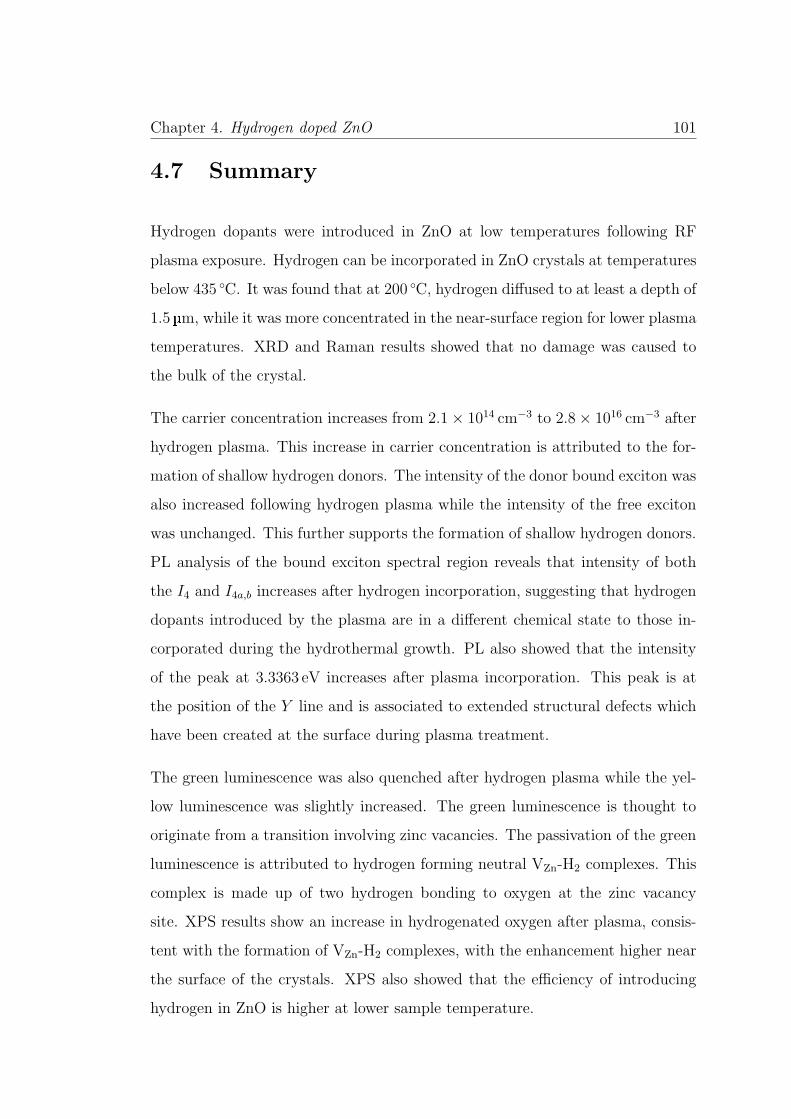
Chapter 4. Hydrogen doped ZnO 101
4.7 Summary
Hydrogen dopants were introduced in ZnO at low temperatures following RF
plasma exposure. Hydrogen can be incorporated in ZnO crystals at temperatures
below 435 ◦C. It was found that at 200 ◦C, hydrogen diffused to at least a depth of
1.5 �m, while it was more concentrated in the near-surface region for lower plasma
temperatures. XRD and Raman results showed that no damage was caused to
the bulk of the crystal.
The carrier concentration increases from 2.1× 1014 cm−3 to 2.8× 1016 cm−3 after
hydrogen plasma. This increase in carrier concentration is attributed to the for-
mation of shallow hydrogen donors. The intensity of the donor bound exciton was
also increased following hydrogen plasma while the intensity of the free exciton
was unchanged. This further supports the formation of shallow hydrogen donors.
PL analysis of the bound exciton spectral region reveals that intensity of both
the I4 and I4a,b increases after hydrogen incorporation, suggesting that hydrogen
dopants introduced by the plasma are in a different chemical state to those in-
corporated during the hydrothermal growth. PL also showed that the intensity
of the peak at 3.3363 eV increases after plasma incorporation. This peak is at
the position of the Y line and is associated to extended structural defects which
have been created at the surface during plasma treatment.
The green luminescence was also quenched after hydrogen plasma while the yel-
low luminescence was slightly increased. The green luminescence is thought to
originate from a transition involving zinc vacancies. The passivation of the green
luminescence is attributed to hydrogen forming neutral VZn-H2 complexes. This
complex is made up of two hydrogen bonding to oxygen at the zinc vacancy
site. XPS results show an increase in hydrogenated oxygen after plasma, consis-
tent with the formation of VZn-H2 complexes, with the enhancement higher near
the surface of the crystals. XPS also showed that the efficiency of introducing
hydrogen in ZnO is higher at lower sample temperature.

Chapter 4. Hydrogen doped ZnO 102
XANES results show that hydrogen interacts only with oxygen atoms in the
lattice and not zinc. This indicates that most of the interstitial hydrogen incor-
porated by plasma treatment sit at the anti-bonding site of the oxygen atom,
with the hydrogen attached to a host oxygen atom and pointing away from the
ZnO bond.

Chapter 5
Hydrogen States and
Recombination Kinetics in ZnO
5.1 Introduction
Optical properties of semiconductors are most often reported at ∼4K. In this
chapter the temperature dependence of the luminescence of ZnO from 10K to
300K and the various mechanisms of thermal quenching are investigated. Neg-
ative thermal quenching of the NBE emission in hydrogen doped ZnO will be
introduced and a model involving shallow traps presented.
The recombination processes of excited electron-hole pairs by examining the re-
lationship between excitation density and luminescence emitted and temperature
dependence of emitted bands is also investigated.
The yellow luminescence in ZnO is often attributed to lithium impurities occu-
pying zinc sites (LiZn). It will be shown that the yellow luminescence in the
ZnO crystals used in this work can be attributed to radiative recombinations in-
volving LiZn. The interaction of hydrogen with lithium impurities leading to the
formation of hydrogen-lithium complexes is also investigated.
103

Chapter 5. Hydrogen States and Recombination Kinetics in ZnO 104
Finally the stability and electro-migration of hydrogen dopants under the electron
beam in ZnO will be investigated.
5.2 Temperature Dependence of the Lumines-
cence
Figure 5.1 shows the CL spectra of both the doped and H-doped ZnO crystals.
The H-doped crystal has been exposed to the hydrogen plasma for 120 s while
the crystal was being kept at 200 ◦C. These conditions were used because at that
temperature hydrogen is still being incorporated in the lattice and the temper-
ature is enough to anneal out some of the damage caused by the plasma (See
Section 4.4 for a more in-depth discussion).
The CL for both as-received and H-doped crystals show similar features namely
the neutral donor bound exciton (D0X) and the first two phonon replicas of the
free exciton luminescence: FX-1LO and FX-2LO. The FX emission is virtually
unchanged at low temperatures while the D0X emission increases considerably.
The intensity of the H-doped crystal is higher than that of the as-received one
for all temperatures. This is consistent with the formation of new shallow donor
levels after hydrogen incorporation. With increasing temperature, the emission
peaks get broader and red-shift. The intensity of the D0X emission decreases
with increasing temperature and the D0X peak is not present at temperatures
above 120K. This is consistent with the neutral donors responsible for that
luminescence being thermally ionised with increasing temperature. The red shift
of the D0X peak can be attributed to successive ionisation of bound exciton.
Bound exciton emissions have localisation energies ranging from 3meV to 27meV
[27]. Emissions with low localisation energies (e.g. I4) will be thermally ionised
first while emissions with higher localisation energies (e.g. I9) are still present

Chapter 5. Hydrogen States and Recombination Kinetics in ZnO 105
3.40 3.35 3.30 3.25 3.20 3.15 3.10
Inte
nsity
(a.u
)
Energy (eV)
300 K
280 K
260 K
240 K
220 K
200 K
180 K
160 K
140 K
120 K
100 K
90 K
80 K
70 K
60 K
50 K
40 K
30 K
20 K
10 K
(a)
D0X
FX-1LO
FX-2LO
D0X
FX-1LO
FX-2LO
As-received
3.40 3.35 3.30 3.25 3.20 3.15 3.10
H-doped
D0X-2LO
(b)
Energy (eV)
FX-3LO
D0X-1LO
Figure 5.1: Temperature dependent CL spectra of the NBE region of (a) as-received and (b) H-doped ZnO taken from 10K to 300K. The arrows show theshifts in the CL peaks with increasing temperature. The plots are verticallyshifted for clarity. All spectra were collected with a beam energy of 15 keV andbeam current of 5.7 nA.

Chapter 5. Hydrogen States and Recombination Kinetics in ZnO 106
unionised at higher temperatures. This then leads to a red-shift of the whole
D0X peak.
It was also found that the dominant luminescence peak in the CL spectra is
the FX-1LO at temperatures above ∼200K. As the average kinetic energy of
free excitons increases with rising temperature, the thermal redistribution leads
to a smaller number of free excitons near the centre of the Brillouin zone, thus
enhancing the participation of LO phonons in the radiative recombination. The
strong LO-phonon-exciton coupling is consistent with the reported PL data of
ZnO at elevated temperatures [176, 177].
The energy separation between the FX and phonon replica (FX-1LO and FX-
2LO) emission peaks exhibit strong temperature dependence. Considering the
spectral line shape of the phonon replicas, the spectral line shape F for the first
LO phonon replica of the free exciton has the form [177–179]:
F (ε) ∼ ε12 exp
( −εkBT
)W (ε) (5.1)
where ε is defined as hν −EFX− hωLO and W (ε) is the transition probability for
the phonon-assisted emission. The form assumed for the probability W (ε) then
determines the energy separation between the FX and the phonon replica. Let
W (ε) vary as εp, where p is a constant. The peak energy of the phonon replica are
then shifted by (p+1/2)kBT to higher energy. At low temperatures, the probability
rate W (ε) for the FX-1LO is assumed to be proportional to ε, implying p = 1
[178]. The peak of the FX-1LO will then be shifted by (1 + 1/2)kBT = 3/2kBT
to higher energies. The energy position of the peak of the FX-1LO can then be
written as:
EFX-1LO = Eg(T )− Eex − hωLO +3
2kBT (5.2)
where Eg(T ) is the bandgap at temperature T , Eex is the temperature indepen-
dent exciton binding energy with a value of 60meV [180] and hωLO is the LO
phonon energy of 72meV.

Chapter 5. Hydrogen States and Recombination Kinetics in ZnO 107
For the FX-2LO, the transition probability is a constant, implying that W (ε)
varies as ε0. Thus p = 0 and the peak energy of the FX-2LO emission is shifted
by (0 + 1/2)kBT = 1/2kBT to higher energies. The energy position of the peak of
the FX-2LO can then be written as:
EFX-2LO = Eg(T )− Eex − 2hωLO +1
2kBT (5.3)
The energy shifts of the FX-1LO and FX-2LO at a temperature T are illustrated
in Figure 5.2.
h LO h LO
kk
FX
FX-1LOFX-2LO
E
Figure 5.2: Temperature dependence of the peak energy position of thephonon replica. The dashed lines are the predicted energy and the full linesare the actual measured energies.
The position of the free exciton peaks for both the as-received and H-doped
crystals were determined from the positions of the FX-1LO and FX-2LO using
Equations 5.2 and 5.3. The energy position of the FX is given by the following
relation:
EFX = Eg − Eex (5.4)
Chapter 5. Hydrogen States and Recombination Kinetics in ZnO 108
0 50 100 150 200 250 300
3.20
3.22
3.24
3.26
3.28
3.30
3.32
3.34
3.36
3.38 As-received FXAs-received fitH-doped FXH-doped fitAs-received FX-1LOH-doped FX-1LOAs-received FX-2LOH-doped FX-2LO
Peak
Posi
tion
(eV)
Temperature (K)
Figure 5.3: Temperature dependence of the FX, FX-1LO and FX-2LO ofthe as-received and H-doped ZnO crystals. The lines are Varshni fits to theexperimental data based on Equation 5.5.
The Varshni relation was then used to fit the temperature dependence of the peak
position of the FX and has the form [29]:
Eg(T ) = Eg(0)− αT 2
T + β(5.5)
where Eg(T ) is the energy gap at temperature T, Eg(0) is the energy gap at 0K,
α and β are empirically measured constants. Typical values of α and β for ZnO
are 5× 10⁻⁴ eV/K and 900K respectively [30].
The calculated energy position of the FX was found to be 3.375 eV for the as-
received ZnO and 3.376 eV for the H-doped one. These energy positions of the
FX emission match those of 3.375 eV to 3.378 eV reported in the literature very
well [27, 58, 181]. The temperature variation of the FX peak energy also follows
the Varshni relation. The Varshni parameters α and β obtained from the fits
are reported in Table 5.1. The parameters for both the as-received and H-doped

Chapter 5. Hydrogen States and Recombination Kinetics in ZnO 109
Table 5.1: Varshni fit parameters for the NBE luminescence peaks
Peak α (eV/K) β (K)
Free exciton from Ref [30] 5.05× 10⁻⁴ 900As-received FX 7.19× 10⁻⁴ 776Doped FX 6.75× 10⁻⁴ 790
ZnO are similar with α being 7.19× 10⁻⁴ eV/K and 6.75× 10⁻⁴ eV/K for the as-
received and H-doped ZnO respectively; and values of β being 776K and 790K
for the as-received and H-doped ZnO respectively as is expected from the similar
positions of the FX and the phonon replica. A slight deviation from the fit is
observed above 200K due to the uncertainty in determining the peak position
resulting from temperature broadening and overlap of the LO phonon replicas.
The measured energy positions of the D0X and FX emissions are presented in
Figure 5.4. The energy separation between the D0X and the FX is constant. This
is expected as the bound excitons follow the following energy relation:
EDX = Eg − Eex − Eloc (5.6)
where Eloc is the localisation energy of the bound exciton. The localisation energy
is the energy separation between the D0X emission and the free exciton emission.
The average localisation energy of the bound exciton is calculated to be 23meV
for the as-received crystals and 19meV for the H-doped one. The shift is con-
sistent with the PL measurements which found a blue-shift of the main bound
exciton peak following hydrogen doping (see Figure 4.6). The increase in the
energy separation at higher temperatures can be explained by thermal ionisation
of bound excitons of localisation energy lower than the thermal energy e.g. I4 to
form free excitons. The bound excitons with higher localisation energies e.g I9
will still be bound and this explains the increase in the energy separation between
the FX and BX peak with increasing temperature.
The intensities of the various NBE peaks as well as for the DLE were extracted

Chapter 5. Hydrogen States and Recombination Kinetics in ZnO 110
0 50 100 150 200 250 3003.26
3.28
3.30
3.32
3.34
3.36
3.38
As-received FXH-doped FXAs-received D0XH-doped D0X
Pea
kP
ositi
on(e
V)
Temperature (K)
Figure 5.4: Temperature dependence FX and D0X for both the as-receivedand H-doped crystals.
from the temperature dependent CL spectra. Figure 5.5 shows the intensity
of the D0X, FX-1LO and FX-2LO emission peaks as a function of temperature
for both the as-received and H-doped ZnO crystals. The intensity of the FX
could not be extracted accurately due to its small intensity. The broadening
of the peaks with increasing temperature makes finding the peak position for
the FX-2LO, and hence its intensity, accurately difficult after 200K. For the
as-received crystal, the intensities of all three peaks decrease with increasing
temperature, with the D0X peak being annealed out at 150K and merging with
the FX-1LO peak, which is the main peak at room temperature as can be seen in
Figure 5.1. The H-doped crystal shows a different temperature dependence to the
as-received one. The intensity of the D0X peak decreases from 10K to 120K. The
intensity however increases for temperatures higher than 120K until the emission
disappears because of the thermal ionisation of the donors. A similar behaviour

Chapter 5. Hydrogen States and Recombination Kinetics in ZnO 111
0 50 100 150 200 250 300 0 50 100 150 200 250 300
D0XFX-1LOFX-2LO
CL
Inte
nsity
(a.u
.)
Temperature (K)
(a) As-received
Temperature (K)
(b) H-doped
Figure 5.5: Temperature dependence of the D0X, FX-1LO and FX-2LO peakintensities for (a) the as-received and (b) H-doped crystals. The H-dopedsample exhibits a negative thermal quenching behaviour.
is seen for both the FX-1LO and FX-2LO. The intensity of those luminescence
peaks decrease with increasing temperature in the range 10K ≤ T ≤ 90K,
the intensity then increases in the range 90K < T ≤ 220K and the intensity
decreases for temperatures above 220K. This behaviour is a unusual and often
called a negative thermal quenching (NTQ) behaviour. This NTQ effect will be
discussed further in the following section (Section 5.3).
A similar investigation of the temperature dependence of the DLE was made.
Figure 5.6 shows the integrated intensities of the yellow and green luminescences
for both the as-received and H-doped crystals. Both the yellow and green lumi-
nescence follow the normal thermal quenching behaviour for both the as-received
and H-doped crystals. This behaviour is similar to the NBE luminescence of the

Chapter 5. Hydrogen States and Recombination Kinetics in ZnO 112
as-received crystal.
0 50 100 150 200 250 300
As-receivedH-Doped
CL
Inte
nsity
(a.u
.)
Temperature (K)
(a) Yellow Luminescence
0 50 100 150 200 250 300
(b) Green Luminescence
CL
Inte
nsity
(a.u
.)
Temperature (K)
Figure 5.6: Temperature dependence of the CL intensity of the (a) yellow and(b) green luminescence for the as-received and H-doped crystal. The H-dopedcrystal does not exhibit a NTQ behaviour in the DLE.
5.3 Negative Thermal Quenching of the NBE
Luminescence
The intensity of the luminescence (e.g. from PL and CL) in solids, such as semi-
conductors and ionic crystals, is normally expected to decrease with increasing
temperature. This phenomenon is known as “thermal quenching” of the lumi-
nescence. The basic mechanism behind the thermal quenching phenomenon is
that non-radiative recombination probability of electrons and holes increase with
increasing temperature [182, 183].
Chapter 5. Hydrogen States and Recombination Kinetics in ZnO 113
It has been reported that for GaAs, in a moderately high temperature range,
the intensity of the luminescence increases with increasing temperature [184].
This abnormal phenomenon is called “negative thermal quenching” (NTQ). The
physical origin of NTQ is thought to be due to the thermal activation of electrons
from the levels with energy smaller than that of the initial state of the radiative
transition or by the release of carriers or excitons from trap states with increasing
temperature. Shibata (1998) has proposed an analytical formula to describe the
temperature dependence of the luminescence intensity of a system which exhibits
the NTQ phenomenon [185]:
I(T ) = I(0)
⎡⎢⎢⎣1 +
w∑q=1
Dq exp(−E ′q/kbT )
1 +m∑j=1
Cj exp(−Ej/kbT )
⎤⎥⎥⎦ (5.7)
where I(T ) is the intensity of the luminescence at temperature T , w is total
number of intermediate states responsible for the NTQ behaviour, each having
the activation energy E ′q, m is the total number of non-radiative recombination
processes, each having the activation energy Ej and C and D are constants
which describe the relative contributions of the different activation processes.
This formula enables quantitative analysis of the mechanisms of the NTQ and
allows determining the activation energies associated with intermediate states as
well as non-radiative states.
Recently this negative thermal quenching behaviour has been observed in both
as-grown and doped ZnO crystals and nanostructures. Watanabe et al. (2006)
reported on this NTQ behaviour in hydrothermal grown ZnO crystals from Crys-
Tec, EaglePicher, and TOKYO DENPA, and in as-received epitaxial ZnO single
crystals grown by radical-source molecular beam epitaxy [186]. While no mecha-
nism was proposed, a series of activation energies for the different processes was
calculated by using Equation 5.7. Wu et al. (2012) reported on the NTQ of the
3.338 eV emission in ZnO nanorods [187]. They proposed a transition from the

Chapter 5. Hydrogen States and Recombination Kinetics in ZnO 114
3.338 eV emission to the surface exciton recombination at 3.368 eV via trap states
which are activated with temperature. While not a NTQ of the luminescence,
Singh et al. (2013) reported a similar increase in the conductivity of hydrogen
doped ZnO thin films with increasing temperature [188]. They have attributed
this behaviour to metal-semiconductor transitions. Above the transition tem-
perature, the ZnO film acts as a degenerate semiconductor because of the high
hydrogen doping levels. With increasing hydrogen doping, the defect band even-
tually overlaps with the conduction band creating a degenerate semiconductor.
This leads to delocalisation of electrons and consequently metallic conductivity
and an increase of the measured conductivity.
The activation energy of the non-radiative traps for the as-received crystal was
calculated by applying a non-linear least square fit to the integrated NBE lumi-
nescence data using Equation 5.7 in the following form:
I(T ) =I(0)
1 + C exp(−E/kbT )(5.8)
This equation represents the formula commonly used to analyse the thermal
quenching phenomenon in systems which do not exhibit NTQ behaviours. Fitting
this equation to the integrated NBE region of the as-received ZnO crystal, an
activation energy, E, of 11.6meV was extracted and the fit shown in Figure 5.7.
This activation energy matches well with reported binding energies of excitons
to defects or traps which are in the range of 10meV to 20meV [135, 189].
To analyse the temperature dependence for the NBE luminescence of the H-
doped sample, Equation 5.7 was rearranged in the following forms for different
temperature ranges:
I(T ) = I(0)
⎡⎣ 1 +D exp(−E ′/kbT )1 + C1 exp(−E1/kbT )
⎤⎦ or I(T ) =
I(0)
1 + C2 exp(−E2/kbT )
for 10K ≤ T ≤ 320K for T > 320K
(5.9)

Chapter 5. Hydrogen States and Recombination Kinetics in ZnO 115
0 100 200 300 400 500 600 700 800
E2 = 18.7 meV
CL
Inte
nsity
(a.u
.)
Temperature (K)
As-receivedH-Doped
E1 = 6.5 meV
E' = 76.7 meV
E = 11.6 meV
Figure 5.7: CL intensity of the integrated NBE luminescence from 10K to800K for the as-received and H-doped crystals. The H-doped crystals exhibitsa clear NTQ behaviour in the range 140K to 320K. The lines show the fits ofthe luminescence based on Equation 5.7.
In this case, the NTQ behaviour is taken into account in the formula. The
numerator part of the formula contains the activation energy of the intermediate
states E ′ while the denominator contains the activation energy E of the non-
radiative traps. Two energies E1 and E2 were used to determine the activation
energies of the non-radiative processes for 10K < T ≤ 140K and T > 320K.
The fits in Figure 5.7 resulted in values of activation energies of E1 = 6.54meV
for the temperature range 10K < T ≤ 140K, E2 = 18.7meV for temperature
T > 320K, and E ′ = 76.7meV for the range 140K < T ≤ 320K for the H-doped
crystal. While the values of E1 and E2 are still in the range of activation energies
of excitons binding to defects or traps, the different energies however indicate a
different thermal quenching mechanism or trap. The high activation energy of
76.7meV indicates that the NTQ mechanism is not solely a thermal process and
must involve other intermediate states.

Chapter 5. Hydrogen States and Recombination Kinetics in ZnO 116
The negative thermal quenching behaviour of the NBE following hydrogen incor-
poration might be attributed to the following mechanisms:
1. introduction of additional recombination channels via neutral donor bound
exciton emission at H-related shallow donor states, known as the I4 line.
2. elimination of the competitive radiative recombination channel by the for-
mation of H complexes with the green luminescence centre.
3. release of electrons from H-related traps which then bind with holes to form
excitons.
4. release of electrons from shallow traps which are then captured by deep
traps, eliminating this pathway.
Introduction of additional recombination channels, e.g. enhancement of the I4
line, and elimination of competitive radiative channels are unlikely causes for the
NTQ behaviour. No new peaks were found in high resolution low temperature
PL meaurements (see Section 4.4.1). Moreover, passivation of competitive radia-
tive channels is also unlikely because shallow donors in ZnO would likely have
already been thermally ionised at 150K and not be able to take part in radia-
tive recombinations. This is because of their localisation energies in the range of
10meV to 15meV which is lower than the thermal energy at 150K. This leaves
the possibility of H-related traps or other shallow traps releasing carriers with
increase in temperature as a possible explanation for the NTQ behaviour.
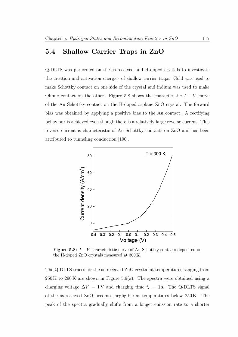
Chapter 5. Hydrogen States and Recombination Kinetics in ZnO 117
5.4 Shallow Carrier Traps in ZnO
Q-DLTS was performed on the as-received and H-doped crystals to investigate
the creation and activation energies of shallow carrier traps. Gold was used to
make Schottky contact on one side of the crystal and indium was used to make
Ohmic contact on the other. Figure 5.8 shows the characteristic I − V curve
of the Au Schottky contact on the H-doped a-plane ZnO crystal. The forward
bias was obtained by applying a positive bias to the Au contact. A rectifying
behaviour is achieved even though there is a relatively large reverse current. This
reverse current is characteristic of Au Schottky contacts on ZnO and has been
attributed to tunneling conduction [190].
Figure 5.8: I − V characteristic curve of Au Schottky contacts deposited onthe H-doped ZnO crystals measured at 300K.
The Q-DLTS traces for the as-received ZnO crystal at temperatures ranging from
250K to 290K are shown in Figure 5.9(a). The spectra were obtained using a
charging voltage ΔV = 1V and charging time tc = 1 s. The Q-DLTS signal
of the as-received ZnO becomes negligible at temperatures below 250K. The
peak of the spectra gradually shifts from a longer emission rate to a shorter

Chapter 5. Hydrogen States and Recombination Kinetics in ZnO 118
one with increasing temperature. More charge is emitted from the as-received
ZnO crystal, which is attributable to the addition of charge being trapped as
the free carrier concentration increases with rising temperature. Figure 5.9(b)
shows an Arrhenius plot derived from the Q-DLTS spectra. Analysis of the
Arrhenius plot using the effective mass m∗e = 0.24me [27] reveals a trap position
of Ea = (23± 2)meV and a capture cross section, σ = 2.6× 10⁻¹⁷ cm−2.
Q-DLTS spectra recorded on the H-doped ZnO crystal at temperatures from
130K to 290K are shown in Figure 5.10(a). The traces have a similar shape to
those obtained on the as-received ZnO. However, while no Q-DLTS signal was ob-
tained for the as-received crystal at temperatures below 250K, Q-DLTS spectra
were collected at temperatures down to 130K for the H-doped crystal. The cor-
responding Arrhenius plot for the H-doped crystal is given in Figure 5.10(b). The
Arrhenius plot shows the presence of two linear regions with different slopes, with
a distinct break occurring at ∼220K which is approximately the same tempera-
ture at which the Q-DLTS signal in the as-grown crystal completely disappears.
Two defect states can be determined from the slopes of the Arrhenius plot with
activation energies Ea of (22± 4)meV and (11± 2)meV with capture cross sec-
tions σ of 4.3× 10⁻¹⁷ cm−2 and 3.9× 10⁻¹⁷ cm−2 respectively.
To index Q-DLTS peaks, the subscript of E is used to indicate the energy level of
a trap in meV. The activation energy of the E22 state is within the experimental
error of the state energy for the as-grown crystal (E23); both can therefore be as-
signed to the same trap. The slight increase in the capture cross section of the E23
trap after hydrogen plasma might be due to the reduction in the number of com-
petitive traps as the ZnO crystals surface is passivated by hydrogen. The lower
energy state at 11meV in the H-doped ZnO crystal is attributed to a sub-surface
state introduced by the hydrogen plasma. While Q-DLTS itself cannot deter-
mine whether carriers in this trap are thermally activated to the valence band or
conduction band, the coincidence of the H-related shallow state formation and
the increase in electron density as revealed by the Hall effect measurement (see

Chapter 5. Hydrogen States and Recombination Kinetics in ZnO 119
(a) Q-DLTS spectra
(b) Arrhenius plot
Figure 5.9: (a) Q-DLTS spectra obtained from the as-received ZnO crystalin the temperature range of 250K to 300K using charging voltage ΔV = 1Vand charging time tc = 1 s (b) Arrhenius plot derived from the data in (a)indicating a state with an average energy of (23± 2)meV.

Chapter 5. Hydrogen States and Recombination Kinetics in ZnO 120
(a) Q-DLTS spectra
(b) Arrhenius plot
Figure 5.10: (a) Q-DLTS spectra obtained from the H-doped ZnO crystalin the temperature range of 130K to 290K using charging voltage ΔV = 1Vand charging time tc = 1 s (b) Arrhenius plot derived from the data in (a) twostates with energies of (22± 4)meV and (11± 2)meV.
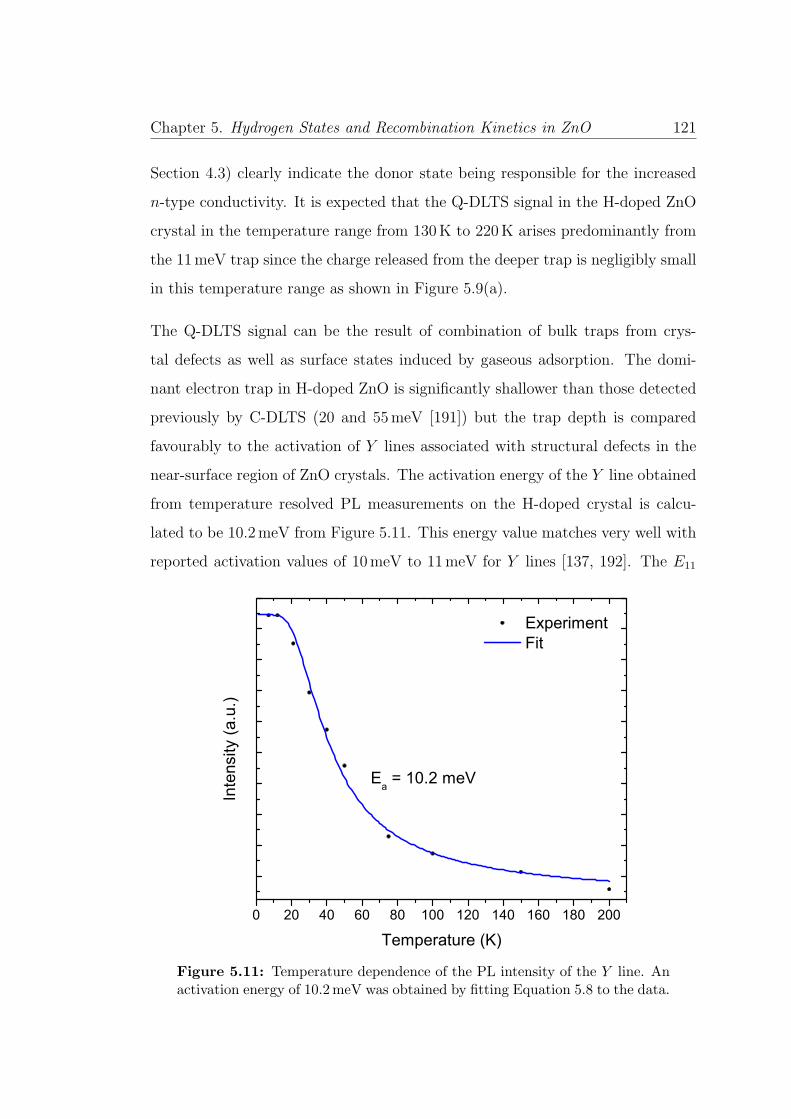
Chapter 5. Hydrogen States and Recombination Kinetics in ZnO 121
Section 4.3) clearly indicate the donor state being responsible for the increased
n-type conductivity. It is expected that the Q-DLTS signal in the H-doped ZnO
crystal in the temperature range from 130K to 220K arises predominantly from
the 11meV trap since the charge released from the deeper trap is negligibly small
in this temperature range as shown in Figure 5.9(a).
The Q-DLTS signal can be the result of combination of bulk traps from crys-
tal defects as well as surface states induced by gaseous adsorption. The domi-
nant electron trap in H-doped ZnO is significantly shallower than those detected
previously by C-DLTS (20 and 55meV [191]) but the trap depth is compared
favourably to the activation of Y lines associated with structural defects in the
near-surface region of ZnO crystals. The activation energy of the Y line obtained
from temperature resolved PL measurements on the H-doped crystal is calcu-
lated to be 10.2meV from Figure 5.11. This energy value matches very well with
reported activation values of 10meV to 11meV for Y lines [137, 192]. The E11
0 20 40 60 80 100 120 140 160 180 200
Inte
nsity
(a.u
.)
Temperature (K)
Experiment Fit
Ea = 10.2 meV
Figure 5.11: Temperature dependence of the PL intensity of the Y line. Anactivation energy of 10.2meV was obtained by fitting Equation 5.8 to the data.

Chapter 5. Hydrogen States and Recombination Kinetics in ZnO 122
trap energy also matches the activation energy of the Y lines well and is much
smaller than the ionisation energy of H shallow state (Ei(H) = 47meV to 53meV
[98, 147]) or the localisation energy of Y lines (Eloc ∼ 47meV [27, 137]).
Both hydrogen and Y line structural defects can introduce additional shallow
donor states in ZnO. In highly doped semiconductors, effects such as Burstein-
Moss and free-carrier screening could have a prominent influence on the NBE
emission. However, these effects are negligible since there is no spectral shift of
the BX and FX peaks after H incorporation. Since hydrogen can diffuse up to
1.5 �m in the crystal (see Section 4.4.5.2), and the activation energy of the E11
trap matches that of the Y lines, the E11 can be attributed to Y line structural
defects in the near-surface region of the crystal caused by hydrogen plasma. The
negative thermal quenching behaviour of the H-doped ZnO (see Section 5.3) can
well be explained by a model in which electrons released from the 11meV trap at
temperatures above ∼130K readily bind with holes to form free excitons, leading
to a large enhancement in radiative recombination of FX and its phonon replicas.
The proposed mechanism is illustrated in Figure 5.12.
ConductionBand
Valence Band
Y states(a)
(b)
(c)
FX
Figure 5.12: Proposed mechanism for the NTQ effect. (a) electrons aretrapped at the Y states, (b) electrons are released from the Y states to theconduction band with increasing temperature, (c) the released electron recom-bines with free holes to form FX luminescence.

Chapter 5. Hydrogen States and Recombination Kinetics in ZnO 123
5.5 Recombination Kinetics
In addition to simple spectral collection or depth-resolved analysis (see Sec-
tion 4.4.5), CL can also be used to perform power density dependent measure-
ments. Before doing such measurements, it is necessary to ensure that the electron
beam itself does not damage the samples.
Exposing samples to high flux electron beams can lead to electron beam induced
damage in the form of atomic displacement arising from elastic collisions (knock-
on damage) [193]. There will be a minimum displacement energy, Ed, required
to dislodge an ion in the lattice to form a vacancy-interstitial pair. Those dis-
placement energies for Zn and O are 18.5 eV and 41.4 eV respectively [194]. The
threshold energy, Eth, required for a particle to dislodge an ion from the lattice
is [195]:
Eth = mc2
(√1 +
Ed
2mc2· Mm− 1
)(5.10)
where m is the mass of the incoming particle, M is the mass of the ion being
dislodged, c is the speed of light in vacuum.
From Equation 5.10 and using the appropriate masses for the electron, zinc and
oxygen ions, the minimum energy of the electron beam necessary to cause knock
on damage is 400 keV for Zn ions and 250 keV for O ions. This energy is much
higher that those used in this project and as such direct damage to the samples
from the electron beam is not expected to happen.
In power density measurements, the beam energy (hence the CL generation
depth) is kept constant while the beam current is varied. By increasing the
beam current, a higher number of electron-hole pairs are created as per Equa-
tion 4.1. This provides information on the recombination kinetics. Excitons have
a typical recombination lifetimes of the order of ps to ns [58, 196], while deep
level emissions have recombination times of the order of hundreds of ns to �s
[197, 198].

Chapter 5. Hydrogen States and Recombination Kinetics in ZnO 124
The CL intensity, ICL, follows a power dependency on the beam current Ib in the
following way [199, 200]:
ICL ∝ Imb (5.11)
The exponent m can be found by taking the log of Equation 5.11 to obtain:
log ICL ∝ m · log Ib (5.12)
A plot of the logarithm of the CL intensity versus the logarithm of the beam
current would then be expected to be linear with slope m. This slope is repre-
sentative of each emission type and gives information about the recombination
kinetics and nature of the emission.
For fast recombinations, such as band-to-band or excitonic emission, the value
of m is expected to be ≥ 1 [201], while defect related recombination tend to
have m < 1, with 1⁄2 being typical [202, 203]. Furthermore, if the incident elec-
tron beam power is producing electron-hole pairs faster than the recombination
rate, the emission channel may show saturation effects by exhibiting a non-linear
response at higher beam currents.
Figure 5.13 shows the luminescence of the as-received ZnO crystal in the DLE
region collected at two different beam currents. At the lower current of 13 pA,
the only observable luminescence was the yellow luminescence centered at 1.96 eV
and with a FWHM of 0.56 eV; the NBE and green luminescence were completely
quenched. The peak parameters of that luminescence are identical to the yellow
luminescence in ZnO intentionally doped with lithium (see Section 4.4.4) and
show that the yellow luminescence in the as-received crystals are due to lithium
impurities. At higher beam currents, the DLE is made up of both the yellow
and green components. This can be explained by the difference in recombination
lifetimes of the yellow luminescence and green luminescence. The yellow lumines-
cence centres, while being present in higher concentrations than those responsible
for the green luminescence, have longer recombination lifetimes in the range of �s
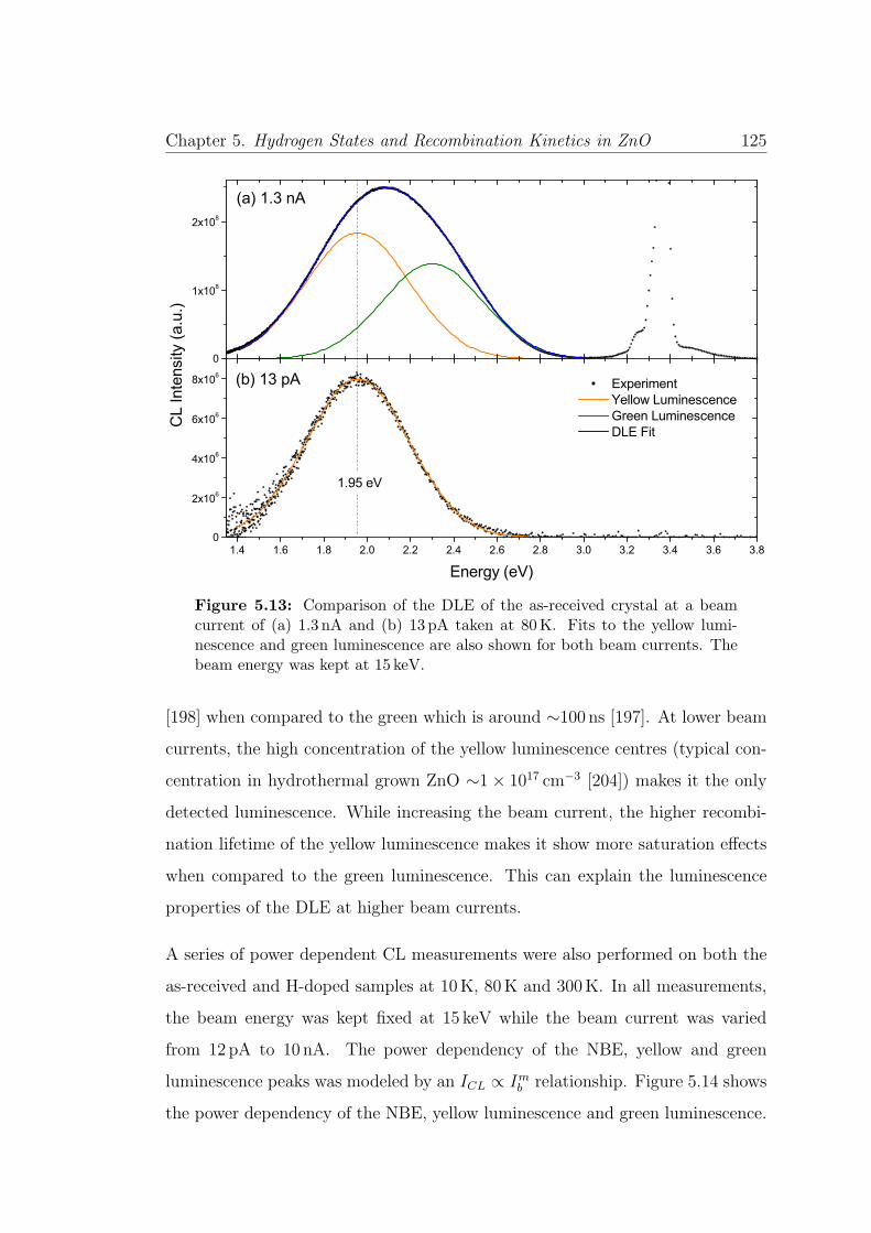
Chapter 5. Hydrogen States and Recombination Kinetics in ZnO 125
0
1x10⁸
2x10⁸
ExperimentYellow LuminescenceGreen LuminescenceDLE Fit
(a) 1.3 nA
1.4 1.6 1.8 2.0 2.2 2.4 2.6 2.8 3.0 3.2 3.4 3.6 3.80
2x10⁶
4x10⁶
6x10⁶
8x10⁶ (b) 13 pA
CL
Inte
nsity
(a.u
.)
Energy (eV)
1.95 eV
Figure 5.13: Comparison of the DLE of the as-received crystal at a beamcurrent of (a) 1.3 nA and (b) 13 pA taken at 80K. Fits to the yellow lumi-nescence and green luminescence are also shown for both beam currents. Thebeam energy was kept at 15 keV.
[198] when compared to the green which is around ∼100 ns [197]. At lower beamcurrents, the high concentration of the yellow luminescence centres (typical con-
centration in hydrothermal grown ZnO ∼1× 1017 cm−3 [204]) makes it the only
detected luminescence. While increasing the beam current, the higher recombi-
nation lifetime of the yellow luminescence makes it show more saturation effects
when compared to the green luminescence. This can explain the luminescence
properties of the DLE at higher beam currents.
A series of power dependent CL measurements were also performed on both the
as-received and H-doped samples at 10K, 80K and 300K. In all measurements,
the beam energy was kept fixed at 15 keV while the beam current was varied
from 12 pA to 10 nA. The power dependency of the NBE, yellow and green
luminescence peaks was modeled by an ICL ∝ Imb relationship. Figure 5.14 shows
the power dependency of the NBE, yellow luminescence and green luminescence.

Chapter 5. Hydrogen States and Recombination Kinetics in ZnO 126
10-10 10-9 10-8
106
107
108
10-10 10-9 10-8105
106
107
108
109
10-10 10-9 10-8
106
107
108
10-10 10-9 10-8
105
106
107
108
109
10-10 10-9 10-8
106
107
108
109
10-11 10-10 10-9
106
107
108
109
NBEYellowGreen
H-dopedC
LIn
tens
ity(a
.u.)
Current (A)
300 K(a) (b) 300 K
(c) 80 K (d) 80 K
(e) 10 K (f) 10 K
As-received
Current (A)
CL
Inte
nsity
(a.u
.)
Current (A) Current (A)
CL
Inte
nsity
(a.u
.)
Current (A) Current (A)
Figure 5.14: Power density measurements of the as-received (a, c, e) andH-doped (b, d, f) crystals at 10K, 80K and 300K. The lines show the powerlaw fit, ICL ∝ Imb , of the data according to Equation 5.11.

Chapter 5. Hydrogen States and Recombination Kinetics in ZnO 127
The lines are the linear fits to the data with the slope of the lines being the
exponent m. The values of m extracted from the fits are summarised in Table 5.2.
It can be seen that the NBE luminescence is increased in the H-doped crystal
compared to the as-received one and is the most intense luminescence at all
temperatures. This result is in accordance to hydrogen forming new shallow
donors while passivating defects.
The NBE luminescence for both as-received and H-doped crystals exhibits a lin-
ear to super-linear (m ≥ 1) dependence on the beam power at all temperatures.
This behaviour is expected and is typical of radiative transitions involving exci-
tons [201]. The power density behaviour of the yellow and green luminescences
however shows high dependencies on temperature.
For the as-received crystals at 300K, both the yellow and green luminescences
show strong sub-linear power dependencies (m ≈ 0.5). This behaviour is not un-
common and is characteristic of radiative transitions involving deep levels. Such
behaviour was observed in other semiconductors and explained through satura-
tion dynamics [200]. Deep-level centres are present in a fixed concentration and
have typical recombination times of the order of hundreds of ns to �s as compared
to excitonic recombinations which are of the order of ps. The long recombination
time of the DLE is caused by their high coupling to the lattice. Increasing the
beam current therefore leads to a saturation of the DLE because they do not
depopulate fast enough to respond to the increase of carriers being injected. This
is reflected in a sub-linear slope (m < 1) of the yellow and green luminescences,
confirming that they originate from radiative recombinations involving deep level
defects.
In the case of the H-doped crystal at 300K, the green luminescence still shows
a strong sub-linear relationship with m = 0.62, while the yellow luminescence is
quenched. The quenching of the yellow luminescence is displayed more clearly in
Figure 5.15 which shows CL spectra of the as-received and H-doped ZnO taken

Chapter 5. Hydrogen States and Recombination Kinetics in ZnO 128
1.4 1.6 1.8 2.0 2.2 2.4 2.6 2.8 3.0 3.2 3.4 3.6
CL
Inte
nsity
(a.u
.)
Energy (eV)
1.4 1.6 1.8 2.0 2.2 2.4 2.6 2.8 3.0
CL
Inte
nsity
(a.u
.)
Energy (eV)
As-received H-doped Green fit Yellow fit
Figure 5.15: CL spectra of the as-received and H-doped crystals taken at300K with a beam energy of 15 keV and beam current of 2 nA. Inset showsthe DLE with fits for the yellow and green luminescences.
at 300K. While the low temperature CL did not show any direct interaction
between hydrogen species and LiZn (see Section 4.4.2), it has been reported that
hydrogen can form neutral complexes with Li impurities in ZnO crystals with
high Li impurity concentration. This can lead to the passivation of LiZn centres
by the formation of neutral LiZn-H complexes [204–206]. The quenching of the
yellow luminescence is therefore attributed to the formation of neutral LiZn-H
complexes.
At 80K, both the yellow and green luminescence of the as-received crystal show
sub linear relationship with beam current. However, the slopes m increase when
compared to those at 300K. After hydrogen doping, the slope of the green
luminescence is unchanged while the yellow luminescence exhibits two slopes.
At lower beam currents (IB < 1 nA), the yellow luminescence responds linearly
with increasing beam current, while at higher beam current (IB > 1 nA), the
slope is sub-linear and similar to that of the green luminescence. Hydrogen
plasma introduces donors in the ZnO crystals. Since the yellow luminescence

Chapter 5. Hydrogen States and Recombination Kinetics in ZnO 129
originates from a DAP recombination involving LiZn, the increase in the donor
concentration reduces the distance between the donor and the LiZn acceptors.
This increases the recombination probability and gives rises to a linear slope. At
higher beam currents, the yellow luminescence starts to saturate owing to the
high recombination time and the slope is sub-linear and comparable to that of
the green luminescence.
At 10K, both the yellow and green luminescence of the as-received crystal again
show sub linear relationship with beam current. The increase in the slope when
compared to both 300K and 80K can be attributed to less donors being ionised,
making the recombination more efficient. It is also possible that the DLE at 10K
differs in mechanism to the one at higher temperatures. Namely being of a DAP
recombination nature at 10K while it is a free to bound at higher temperatures.
However, after hydrogen doping, the yellow luminescence exhibits two slopes
similar to what is observed at 80K. The green luminescence exhibits a single
linear slope after hydrogen doping. The linear slopes after hydrogen doping can
be explained by a higher number of donors being introduced in the vicinity of
both LiZn and VZn, increasing the recombination rate. The two slopes of the
yellow luminescence can again be explained in terms of saturation effects with
increasing beam currents.
Table 5.2: Coefficients of the power density fit of the NBE, yellow and greenluminescences for the as-received and H-doped samples.
Temperature (K) NBE Yellow Green
10KAs-received 1.10± 0.06 0.75± 0.03 0.84± 0.04
H-doped 1.32± 0.071.17± 0.03 (Ib < 0.1 nA)
1.00± 0.040.79± 0.03 (Ib > 0.1 nA)
80KAs-received 1.02± 0.05 0.69± 0.04 0.68± 0.03
H-doped 1.05± 0.060.95± 0.03 (Ib <1 nA)
0.66± 0.040.64± 0.03 (Ib > 1 nA)
300KAs-received 1.10± 0.04 0.44± 0.03 0.53± 0.04H-doped 1.09± 0.05 – a 0.62± 0.04
aThe yellow luminescence was quenched after H plasma.

Chapter 5. Hydrogen States and Recombination Kinetics in ZnO 130
5.6 Characteristics of the Yellow Luminescence
The coupling of electrons to phonon in the yellow luminescence was also stud-
ied. Peak position and full width half maximum (FWHM) values for the yellow
luminescence of the as-received crystal were found at lower beam powers in the
temperature range of 10K to 250K. Lower currents were chosen because the
yellow luminescence is the dominant emission present at those low current values
(see Figure 5.13). Figure 5.16 shows the variation of the FWHM of the yel-
low luminescence peak with temperature. The experimental FWHM data of the
yellow luminescence was fitted to find the Huang-Rhys parameter S using the
relationship [207, 208]:
FWHM = 2.36S�ω
√coth
(�ω
2kT
)(5.13)
where �ω is the mean local photon energy. In the case of strong electron-phonon
coupling (S � 1), S represents the mean number of the emitted phonons for
each photon emitted [134]. The larger the value of S, the wider the band and the
less resolved are transitions corresponding to different vibration levels. Fitting
Equation 5.13 to the data in Figure 5.16 yielded values of S = 8 and �ω = 31meV.
Using the peak energy of the yellow luminescence peak at 1.99 eV measured by
CL, the calculated Huang-Rhys parameter and local phonon energy, the zero
phonon transition for the yellow emission was determined to be at 2.20 eV.
It is believed that the yellow luminescence is dominated by a donor-acceptor
pair (DAP) recombination of a shallow donor to a deep LiZn acceptor at low
temperature or a free to bound recombination at high temperatures. The energy
of such a DAP transition, EDAP , which is equivalent to the zero phonon line, is
given by:
EDAP = Eg − EA − ED +e2
4πε0εrr(5.14)
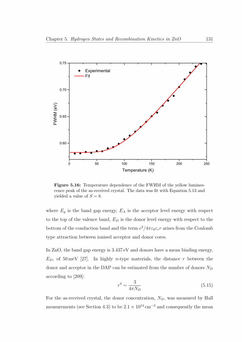
Chapter 5. Hydrogen States and Recombination Kinetics in ZnO 131
0 50 100 150 200 250
0.60
0.65
0.70
0.75
ExperimentalFit
FWH
M(e
V)
Temperature (K)
Figure 5.16: Temperature dependence of the FWHM of the yellow lumines-cence peak of the as-received crystal. The data was fit with Equation 5.13 andyielded a value of S = 8.
where Eg is the band gap energy, EA is the acceptor level energy with respect
to the top of the valence band, ED is the donor level energy with respect to the
bottom of the conduction band and the term e2/4πε0εrr arises from the Coulomb
type attraction between ionised acceptor and donor cores.
In ZnO, the band gap energy is 3.437 eV and donors have a mean binding energy,
ED, of 50meV [27]. In highly n-type materials, the distance r between the
donor and acceptor in the DAP can be estimated from the number of donors ND
according to [209]:
r3 ∼ 3
4πND
(5.15)
For the as-received crystal, the donor concentration, ND, was measured by Hall
measurements (see Section 4.3) to be 2.1× 1014 cm−3 and consequently the mean

Chapter 5. Hydrogen States and Recombination Kinetics in ZnO 132
distance between the donor-acceptor pair was calculated to be ∼50 nm. The
acceptor binding energy, EA, for the yellow luminescence was then calculated
to be 1.18 eV above the conduction band maximum. This energy is compara-
ble to acceptor energies of LiZn found by first principle calculations [210] and
experimentally through electron spin resonance measurements [50]. This shows
that the yellow luminescence in the crystals originates from a radiative transition
involving LiZn centres.
A similar analysis for the green luminescence was not achieved because it was
not possible to isolate the green luminescence owing to overlaps with the yellow
luminescence and the tail from the NBE luminescence with increasing tempera-
ture.
5.7 Stability of Hydrogen Under the Electron
Beam in ZnO
The stability of hydrogen dopants and defect complexes involving hydrogen under
the electron beam was investigated in this work. As-received and H-doped ZnO
crystals were exposed to a low energy electon beam irradiation (LEEBI) while
simultaneously monitoring the CL from the crystals.
LEEBI runs were performed on the as-received and H-doped ZnO crystals with
doping done at 200 ◦C to investigate the stability of the luminescence centres
under the electron beam. To maximise the effect of LEEBI, a high electron beam
power density was used. The electron beam energy was set at 30 keV while the
beam current was set to a high injection rate of 250 nA, with the beam stationary
during irradiation. These beam conditions are much harsher than those used
in the power density CL measurements in Section 5.5 by about two orders of
magnitude.
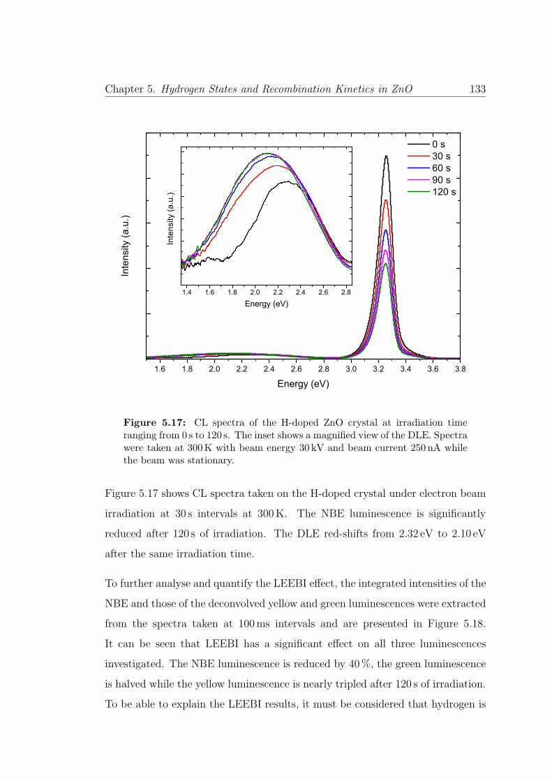
Chapter 5. Hydrogen States and Recombination Kinetics in ZnO 133
1.6 1.8 2.0 2.2 2.4 2.6 2.8 3.0 3.2 3.4 3.6 3.8
In
tens
ity (a
.u.)
Energy (eV)
0 s 30 s 60 s 90 s 120 s
1.4 1.6 1.8 2.0 2.2 2.4 2.6 2.8
Inte
nsity
(a.u
.)
Energy (eV)
Figure 5.17: CL spectra of the H-doped ZnO crystal at irradiation timeranging from 0 s to 120 s. The inset shows a magnified view of the DLE. Spectrawere taken at 300K with beam energy 30 kV and beam current 250 nA whilethe beam was stationary.
Figure 5.17 shows CL spectra taken on the H-doped crystal under electron beam
irradiation at 30 s intervals at 300K. The NBE luminescence is significantly
reduced after 120 s of irradiation. The DLE red-shifts from 2.32 eV to 2.10 eV
after the same irradiation time.
To further analyse and quantify the LEEBI effect, the integrated intensities of the
NBE and those of the deconvolved yellow and green luminescences were extracted
from the spectra taken at 100ms intervals and are presented in Figure 5.18.
It can be seen that LEEBI has a significant effect on all three luminescences
investigated. The NBE luminescence is reduced by 40%, the green luminescence
is halved while the yellow luminescence is nearly tripled after 120 s of irradiation.
To be able to explain the LEEBI results, it must be considered that hydrogen is

Chapter 5. Hydrogen States and Recombination Kinetics in ZnO 134
0 20 40 60 80 100 120
Inte
nsity
(a.u
)
Time (s)
NBE
(a)
0 20 40 60 80 100 120
(b)
Time (s)
YellowGreen
Figure 5.18: Integrated intensities of (a) the NBE luminescence and (b) theyellow and green luminescences of the H-doped ZnO crystal as a function ofLEEBI time taken at 300K. Data points were taken at 100ms interval.
present in the crystal in possibly three configurations, hydrogen interstitial (Hi),
hydrogen complexing with zinc vacancies (VZn-H2), and hydrogen attached to
lithium on a zinc site (LiZn-H). The diffusion barrier for Hi has been reported
to be in the range of 0.1 eV to 0.5 eV [123–125], the dissociation energy of the
VZn-H2 complex has been reported to be 1.8 eV [64], and the dissociation energy
of the LiZn-H complex has been reported to be 2.5 eV [211]. There are several
mechanisms by which these binding energies may be overcome during LEEBI:
1. elastic collisions and momentum transfer between injected electrons and H
impurities.
2. re-absorption of band edge emission (3.37 eV at 300K) [212].
3. electromigration of species under localised electric field.

Chapter 5. Hydrogen States and Recombination Kinetics in ZnO 135
4. localised beam heating.
Re-absorption of the band edge emission can be ruled out because no sign of such
effects was seen in depth-resolved CL measurements. The decrease in the NBE
luminescence can be attributed to mobile Hi being removed from the interaction
volume from the electric fields in the crystal’s surface induced by the beam [213].
While the carrier concentration of the H-doped crystals increases after hydrogen
plasma, the bulk of the crystals have lower carrier concentrations. It is known
that electron irradiation of semi- or insulating materials can lead to the formation
of a charged double layer [214]. In the near surface region, electrons generated
within the secondary electron escape depth are emitted from the surface, leaving
behind a positively charged thin layer. Deeper in the sample, excess electrons
from the main beam are trapped and this region develops a negative charge. The
two regions set up a strong dipole field capable of facilitating electromigration of
mobile defects such as Hi.
The increase in the yellow luminescence can be explained by the dissociation of
LiZn-H complexes under the electron beam. Thermally assisted processes under
the influence of electron beams in SEM on ZnO have been reported [215]. It
was found that at room temperature, the yellow luminescence is quenched in H-
doped ZnO crystals, consistent with the formation of neutral LiZn-H complexes
(see Section 5.5). The dissociation of LiZn-H complexes to LiZn impurities can
explain the increase in the yellow luminescence. On the other hand, the decrease
of the green luminescence can be explained in terms of competition for carriers.
The LiZn centre is a more efficient recombination pathway, therefore the yellow
luminescence increases at the expense of the green luminescence. This explana-
tion is further supported because both the intensities of the yellow luminescence
and green luminescence reach equilibrium after 40 s of beam irradiation. The
increase in the yellow luminescence and the decrease of the green luminescence
is also consistent with the red-shift of the DLE from 2.32 eV to 2.10 eV observed
from Figure 5.17.
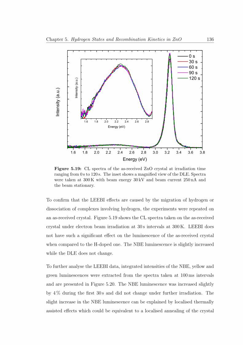
Chapter 5. Hydrogen States and Recombination Kinetics in ZnO 136
1.6 1.8 2.0 2.2 2.4 2.6 2.8 3.0 3.2 3.4 3.6 3.8
Inte
nsity
(a.u
.)
Energy (eV)
0 s30 s60 s90 s120 s
1.6 1.8 2.0 2.2 2.4 2.6 2.8
Inte
nsity
(a.u
.)
Energy (eV)
Figure 5.19: CL spectra of the as-received ZnO crystal at irradiation timeranging from 0 s to 120 s. The inset shows a magnified view of the DLE. Spectrawere taken at 300K with beam energy 30 kV and beam current 250 nA andthe beam stationary.
To confirm that the LEEBI effects are caused by the migration of hydrogen or
dissociation of complexes involving hydrogen, the experiments were repeated on
an as-received crystal. Figure 5.19 shows the CL spectra taken on the as-received
crystal under electron beam irradiation at 30 s intervals at 300K. LEEBI does
not have such a significant effect on the luminescence of the as-received crystal
when compared to the H-doped one. The NBE luminescence is slightly increased
while the DLE does not change.
To further analyse the LEEBI data, integrated intensities of the NBE, yellow and
green luminescences were extracted from the spectra taken at 100ms intervals
and are presented in Figure 5.20. The NBE luminescence was increased slightly
by 4% during the first 30 s and did not change under further irradiation. The
slight increase in the NBE luminescence can be explained by localised thermally
assisted effects which could be equivalent to a localised annealing of the crystal

Chapter 5. Hydrogen States and Recombination Kinetics in ZnO 137
0 10 20 30 40 50 60 70 80 90 100 110 120
Inte
nsity
(a.u
)
Time (s)
NBEGreenYellow
Figure 5.20: Integrated intensities of the NBE luminescence and the yellowand green luminescences of the as-received ZnO crystal as a function of LEEBItime taken at 300K. Data points were taken at 100ms interval.
in the interaction volume. Such effects can lead to an improvement in the crystal
quality and consequently an increase in the NBE luminescence. The yellow and
green luminescence were however practically unchanged over the whole 120 s of
irradiation. The variation in the intensities is attributed to the electron beam
power not being properly stable over the course of the irradiation run.
To confirm the mechanisms taking place during LEEBI, the irradiation experi-
ments on both the as-received and H-doped ZnO crystals were repeated at 10K.
The evolution of the NBE luminescence for the as-received and H-doped ZnO
crystals at both 10K and 300K is shown in Figure 5.21. The NBE luminescence
of the as-received crystal does not show any change throughout the whole 120 s
of irradiation at 10K. The NBE of the H-doped crystal decreases by 70% after
120 s of irradiation at 10K compared to the 40% decrease at 300K. By lowering
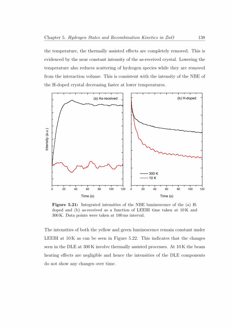
Chapter 5. Hydrogen States and Recombination Kinetics in ZnO 138
the temperature, the thermally assisted effects are completely removed. This is
evidenced by the near constant intensity of the as-received crystal. Lowering the
temperature also reduces scattering of hydrogen species while they are removed
from the interaction volume. This is consistent with the intensity of the NBE of
the H-doped crystal decreasing faster at lower temperatures.
0 20 40 60 80 100 120
Inte
nsity
(a.u
.)
Time (s)
(a) As-received
0 20 40 60 80 100 120
Time (s)
300 K 10 K
(b) H-doped
Figure 5.21: Integrated intensities of the NBE luminescence of the (a) H-doped and (b) as-received as a function of LEEBI time taken at 10K and300K. Data points were taken at 100ms interval.
The intensities of both the yellow and green luminescence remain constant under
LEEBI at 10K as can be seen in Figure 5.22. This indicates that the changes
seen in the DLE at 300K involve thermally assisted processes. At 10K the beam
heating effects are negligible and hence the intensities of the DLE components
do not show any changes over time.

Chapter 5. Hydrogen States and Recombination Kinetics in ZnO 139
0 20 40 60 80 100 120 0 20 40 60 80 100 120
Inte
nsity
(a.u
.)
Time (s)
(a) As-received
Time (s)
Green Yellow
(b) H-doped
Figure 5.22: Integrated intensities of the yellow and green luminescence ofthe (a) as-received and (b) H-doped crystals as a function of LEEBI time takenat 10K. Data points were taken at 100ms interval.
Chapter 5. Hydrogen States and Recombination Kinetics in ZnO 140
5.8 Summary
It was found that the main luminescence at high temperature is dominated by
the phonon replica of the free exciton and not the free exciton luminescence itself.
Moreover, while the as-received crystals show a normal thermal quenching of the
intensity of the NBE luminescence with increasing temperature, the H-doped
crystal exhibits a so-called negative thermal quenching from 130K to 320K. In
samples showing this NTQ behaviour, the intensity of the luminescence tends to
increase with increasing temperature.
An analysis of shallow carrier traps in the as-received ZnO revealed only one
charge trap with activation energy of 23meV. The H-doped crystal exhibits two
carrier traps, one with activation energy of 22meV and another at 11meV. More-
over, the activation energy of the Y lines was found to be 10.2meV from temper-
ature resolved PL measurements. The mechanism for the NTQ is attributed to
hydrogen introducing charge traps at the Y lines which then get thermally ionised
at 130K, releasing electrons which then bind with holes to form free excitons.
This leads to the increase in the NBE luminescence.
The recombination kinetics of the luminescence were also investigated. The NBE
emission shows the expected linear to super-linear relation to beam current in
both the as-received and H-doped crystals. The recombination kinetics of the
yellow and green luminescences however show strong temperature dependencies.
They exhibit a sub-linear relationship at 300K which then becomes linear with
decreasing temperature. This is explained by more shallow donors available at
lower temperatures to take part in radiative recombination.
The characteristics of the yellow luminescence was analysed by temperature re-
solved CL. The peak properties of the yellow luminescence in the as-received ZnO
crystals are identical to the yellow luminescence observed in lithium doped ZnO.

Chapter 5. Hydrogen States and Recombination Kinetics in ZnO 141
The origin of the yellow luminescence is then attributed to radiative recombina-
tions involving LiZn impurities.
Finally, the stability of hydrogen species under high current electron beam ir-
radiation was investigated. Electromigration of hydrogen donors was observed
which leads to a decrease in the intensity of the NBE emission in H-doped ZnO.
Dissociation of neutral LiZn-H complexes to form LiZn was also observed and this
was detected by an increase in the yellow luminescence at the expense of the
green. At 10K only the electromigration of hydrogen donors is observed.

Chapter 6
Conclusions and Future
Directions
6.1 Conclusions
The overall aim of this project was to elucidate the role of hydrogen as a shallow
donor and defect passivator in ZnO. This was achieved by assessing the key
objectives of the research project which were to investigate:
� the effects of hydrogen on the luminescence and electronic properties ofZnO.
� the interaction of hydrogen with native defects and impurities.
� the spatial distribution of luminescence centres and defect related emisionsin ZnO and their origins.
� the stability of hydrogen in ZnO.
The work reported in the previous chapters addressed these objectives and can
be summarised as follows.
142

Chapter 6. Conclusions and Future Directions 143
Incorporation of hydrogen dopants into a-plane ZnO crystals at low temperature
was achieved through exposure of the crystals to a hydrogen RF plasma source.
The low temperature at which the sample is kept during the hydrogen incorpo-
ration ensures minimal native defect creation in the crystals. Incorporation of
hydrogen in the crystals was confirmed by XPS measurements which revealed an
increase in hydrogenated oxygen ions. Penetration and diffusion depths of hy-
drogen was estimated from depth-resolved cathodoluminescence. Hydrogen was
found to diffuse to at least a depth of 1.5 �m.
The carrier concentration was increased from 2.1× 1014 cm−3 to 2.8× 1016 cm−3
following hydrogen incorporation and was attributed to the formation of H-related
shallow donors. Consequently, the intensity of the donor bound exciton was also
increased following hydrogen plasma while the intensity of the free exciton re-
mained unchanged. High resolution PL analysis of the BX spectral region reveals
that the intensity of both the I4 and I4a,b emissions increase after hydrogen in-
corporation suggesting that hydrogen dopants introduced by the plasma are in a
different chemical state to those incorporated during the hydrothermal growth.
PL also showed that the intensity of the peak at 3.3363 eV increases after plasma
incorporation. This peak called the Y line, is associated to extended structural
defects which have been created at the surface during plasma treatment. Tem-
perature dependent PL measurements determined the activation energy of the Y
line to be ∼10.2meV.
The NBE luminescence of the H-doped crystal exhibits negative thermal quench-
ing from 130K to 320K, whereby the intensity of the emission increases with in-
creasing temperature. An analysis of shallow carrier traps in the as-received ZnO
revealed only one charge trap with activation energy of 23meV. The H-doped
crystal showed the presence of two carrier traps, one with activation energy of
22meV and another at 11meV. The mechanism for the NTQ is attributed to hy-
drogen introducing charge traps at the Y lines which then get thermally ionised
at 130K, releasing electrons which then bind with holes to form free excitons.
Chapter 6. Conclusions and Future Directions 144
The defect luminescence commonly found in ZnO was also highly affected by
hydrogen incorporation. The green luminescence was quenched after hydrogen
plasma while the yellow luminescence was slightly increased. The green lumi-
nescence is thought to originate from a transition involving zinc vacancies. The
passivation of the green luminescence is attributed to hydrogen forming neutral
VZn-H2 complexes. This complex is made up of two hydrogen bonding to oxygen
at the zinc vacancy site. XPS results show an increase in hydrogenated oxygen
after plasma, consistent with the formation of VZn-H2 complexes. The yellow
luminescence in the as-received crystals is identical to that in lithium doped ZnO
and is attributed to a radiative recombination involving LiZn impurities.
The recombination kinetics of the luminescence were also investigated. The NBE
emission shows the expected linear to super-linear relation to beam current in
both the as-received and H-doped crystals. The recombination kinetics of the
yellow and green luminescences however show strong temperature dependencies.
They exhibit a sub-linear relationship at 300K which then becomes linear with
decreasing temperature. This is explained by more shallow donors available at
lower temperatures to take part in radiative recombination.
XANES results showed that hydrogen interacts only with oxygen atoms in the
lattice and not zinc. This indicates that most of the interstitial hydrogen incor-
porated by plasma treatment sit at the anti-bonding site of the oxygen atom,
with the hydrogen attached to a host oxygen atom and pointing away from the
Zn−O bond.
Finally, the stability of hydrogen species under high current electron beam ir-
radiation was investigated. Electromigration of hydrogen donors was observed
which leads to a decrease in the intensity of the NBE emission in H-doped ZnO.
Dissociation of neutral LiZn-H complexes to form LiZn was also observed and this
was detected by an increase in the yellow luminescence at the expense of the
green. At 10K only the electromigration of hydrogen donors is observed while

Chapter 6. Conclusions and Future Directions 145
the yellow and green luminescence remained constant throughout the irradiation
time. This indicates that dissociation of the LiZn-H complexes at 300K involves
thermally assisted processes.
6.2 Future Directions
There are some areas touched on during the course of this work that could be the
focus for further research. Nanostructures, such as nanoparticles and nanowires,
are known to have significantly different optical properties to bulk material owing
to their high surface to volume ratio. As plasma treatment is primarily a surface
modification technique, it would be interesting to investigate the optical prop-
erties of nanostructured ZnO following plasma treatments in hydrogen or other
gaseous environments.
It is thought that hydrogen is the cause of the intrinsic n-type character of as-
grown ZnO. LEEBI experiments have shown that hydrogen dopants are not stable
under electron irradiation. This property can be used to control and modify the
concentration of hydrogen impurities in ZnO. Intentional co-doping with hydro-
gen could possibly stabilise acceptors in the lattice and subsequent removal of the
hydrogen can lead to successful p-type doping, similar to what is done in GaN
with Mg-H complexes.
From an experimental point of view, studying the incorporation of hydrogen and
its effects on the optical and electrical properties in-situ would be an advantage.
It is possible that changes to the optical and electrical properties are affected by
exposure to air due to surface adsorption of impurities. Doing the incorporation
and characterisation without breaking vacuum in a scanning microscope would
be an interesting project in itself.
Chapter 6. Conclusions and Future Directions 146
6.3 Closing Remarks
ZnO remains a material with potential application in various optoelectronic de-
vices and technologies. The ultimate goal is to develop high quality devices based
on ZnO. The main hurdle to achieving those devices is the challenge of manu-
facturing high quality p-type ZnO. However, the work done in this thesis shows
that hydrogen doped ZnO offers improved optical properties over as-grown ZnO.
This could be used in high quality optical devices. I believe that it is only a
matter of time before ZnO emerges as one of most important solid state lighting
materials. I hope that work done throughout this thesis has contributed to the
understanding of the hurdles holding back ZnO.

Bibliography
[1] Becheri, A., Durr, M., Lo Nostro, P., and Baglioni, P. Synthesis andcharacterization of zinc oxide nanoparticles: application to textiles as UV-absorbers. Journal of Nanoparticle Research, 10(4):679–689, 2008.
[2] Serpone, N., Dondi, D., and Albini, A. Inorganic and organic UV filters:Their role and efficacy in sunscreens and suncare products. InorganicaChimica Acta, 360(3):794–802, 2007.
[3] Carcia, P. F., McLean, R. S., Reilly, M. H., and Nunes, G. TransparentZnO thin-film transistor fabricated by rf magnetron sputtering. Appl. Phys.Lett., 82(7):1117, 2003.
[4] Hoffman, R. L., Norris, B. J., and Wager, J. F. ZnO-based transparentthin-film transistors. Appl. Phys. Lett., 82(5):733, 2003.
[5] Lim, J.-H., Kang, C.-K., Kim, K.-K., Park, I.-K., Hwang, D.-K., and Park,S.-J. UV Electroluminescence Emission from ZnO Light-Emitting DiodesGrown by High-Temperature Radiofrequency Sputtering. Advanced Mate-rials, 18(20):2720, 2006.
[6] Choi, Y.-S., Kang, J.-W., Hwang, D.-K., and Park, S.-J. Recent Advancesin ZnO-Based Light-Emitting Diodes. Electron Devices, IEEE Transactionson, 57(1):26–41, 2010.
[7] Huang, M. H., Mao, S., Feick, H., Yan, H., Wu, Y., Kind, H., We-ber, E., Russo, R., and Yang, P. Room-temperature ultraviolet nanowirenanolasers. Science, 292(5523):1897–9, 2001.
[8] Li, H.-Y., Ruhle, S., Khedoe, R., Koenderink, A. F., and Vanmaekelbergh,D. Polarization, microscopic origin, and mode structure of luminescenceand lasing from single ZnO nanowires. Nano letters, 9(10):3515–20, 2009.
[9] Kavitha, R. and Jayaram, V. Band-Gap Engineering in ZnO-MgO FilmsPrepared by Combustion Flame Pyrolysis of Solution Precursors. Journalof Electronic Materials, 36(10):1326–1332, 2007.
147

Bibliography 148
[10] Ku, C. H., Chiang, H. H., andWu, J. J. Bandgap engineering of well-alignedZn1 - xMgxO nanorods grown by metalorganic chemical vapor deposition.Chemical Physics Letters, 404(1-3):132–135, 2005.
[11] Santana, G., Morales-Acevedo, A., Vigil, O., Vaillant, L., Cruz, F., andContreras-Puente, G. Structural and optical properties of (ZnO)x(CdO)1-xthin films obtained by spray pyrolysis. Thin Solid Films, 373(1-2):235–238,2000.
[12] Fuller, M. L. A method of determining the axial ratio of a crystal fromx-ray diffraction data: the axial ratio and lattice constants of zinc oxide.Science, 70(1808):196–8, 1929.
[13] Dierre, B., Yuan, X. L., Yao, Y. Z., Yokoyama, M., and Sekiguchi, T.Impact of electron beam irradiation on the cathodoluminescence intensityfor ZnO and GaN. Journal of Materials Science: Materials in Electronics,19(S1):307–310, 2008.
[14] Yan, H., Johnson, J., Law, M., He, R., Knutsen, K., McKinney, J., Pham,J., Saykally, R., and Yang, P. ZnO Nanoribbon Microcavity Lasers. Ad-vanced Materials, 15(22):1907–1911, 2003.
[15] Chu, S., Wang, G., Zhou, W., Lin, Y., Chernyak, L., Zhao, J., Kong, J.,Li, L., Ren, J., and Liu, J. Electrically pumped waveguide lasing from ZnOnanowires. Nature nanotechnology, 6(8):506–10, 2011.
[16] Zhang, Y., Russo, R. E. R., and Mao, S. S. S. Quantum efficiency of ZnOnanowire nanolasers. Applied Physics Letters, 87(4):043106, 2005.
[17] Coskun, C., Look, D. C., Farlow, G. C., and Sizelove, J. R. Radiation hard-ness of ZnO at low temperatures. Semiconductor Science and Technology,19(6):752–754, 2004.
[18] Polyakov, a. Y., Smirnov, N. B., Govorkov, a. V., Kozhukhova, E. a.,Vdovin, V. I., Ip, K., Overberg, M. E., Heo, Y. W., Norton, D. P., Pearton,S. J., Zavada, J. M., and Dravin, V. a. Proton implantation effects on elec-trical and recombination properties of undoped ZnO. Journal of AppliedPhysics, 94(5):2895, 2003.
[19] Kim, A., Won, Y., Woo, K., Kim, C.-h., and Moon, J. Highly Transpar-ent Low Resistance ZnO/Ag Nanowire/ZnO Composite Electrode for ThinFilm Solar Cells. ACS nano, 7(2):1081–91, 2013.
[20] Matsubara, K., Fons, P., Iwata, K., Yamada, a., Sakurai, K., Tampo, H.,and Niki, S. ZnO transparent conducting films deposited by pulsed laserdeposition for solar cell applications. Thin Solid Films, 431-432:369–372,2003.
Bibliography 149
[21] Jaffe, J. E. and Hess, A. C. Hartree-Fock study of phase changes in ZnOat high pressure. Physical review. B, Condensed matter, 48(11):7903–7909,1993.
[22] Wang, Z. L. Zinc oxide nanostructures: growth, properties and applications.Journal of Physics: Condensed Matter, 16(25):R829–R858, 2004.
[23] Woll, C. The chemistry and physics of zinc oxide surfaces. Progress inSurface Science, 82(2-3):55–120, 2007.
[24] Du, M. H., Zhang, S. B., Northrup, J. E., and Erwin, S. C. Stabilizationmechanisms of polar surfaces: ZnO surfaces. Phys. Rev. B, 78(15):155424–155427, 2008.
[25] Laskowski, R. and Christensen, N. Ab initio calculation of excitons in ZnO.Physical Review B, 73(4):045201, 2006.
[26] Cobet, M., Cobet, C., Wagner, M. R., Esser, N., Thomsen, C., and Hoff-mann, A. Polariton effects in the dielectric function of ZnO excitons ob-tained by ellipsometry. Applied Physics Letters, 96(3):031904, 2010.
[27] Meyer, B. K., Alves, H., Hofmann, D. M., Kriegseis, W., Forster, D.,Bertram, F., Christen, J., Hoffmann, A., Straß burg, M., Dworzak, M.,Haboeck, U., and Rodina, A. V. Bound exciton and donoracceptor pairrecombinations in ZnO. Phys. Status Solidi B, 241(2):231–260, 2004.
[28] Janotti, A. and Van de Walle, C. G. Fundamentals of zinc oxide as asemiconductor. Reports on Progress in Physics, 72(12):126501, 2009.
[29] Varshni, Y. Temperature dependence of the energy gap in semiconductors.Physica, 34(1):149–154, 1967.
[30] Jagadish, C. and Pearton, S. J. Zinc Oxide Bulk, Thin Films and Nanos-tructures: Processing, Properties, and Applications. Elsevier Science, 1edition, 2006.
[31] Janotti, A. and Van de Walle, C. G. Oxygen vacancies in ZnO. AppliedPhysics Letters, 87(12):122102, 2005.
[32] Pfisterer, D., Sann, J., Hofmann, D. M., Meyer, B., Frank, T., Pensl, G.,Tena-Zaera, R., Zuniga Perez, J., Martinez-Tomas, C., and Munoz Sanjose,V. Negative U-properties of the oxygen-vacancy in ZnO. Physica StatusSolidi (C), 3(4):997–1000, 2006.
[33] Erhart, P., Klein, A., and Albe, K. First-principles study of the structureand stability of oxygen defects in zinc oxide. Physical Review B, 72(8):085213, 2005.

Bibliography 150
[34] Paudel, T. and Lambrecht, W. First-principles calculation of the O vacancyin ZnO: A self-consistent gap-corrected approach. Physical Review B, 77(20):205202, 2008.
[35] Erhart, P., Albe, K., and Klein, A. First-principles study of intrinsic pointdefects in ZnO: Role of band structure, volume relaxation, and finite-sizeeffects. Physical Review B, 73(20):205203, 2006.
[36] Oba, F., Togo, A., and Tanaka, I. Defect energetics in ZnO: A hybridHartree-Fock density functional study. Physical Review B, 77(24):245202,2008.
[37] Janotti, A. and Van de Walle, C. G. Hydrogen multicentre bonds. Nat.Mater., 6(1):44–47, 2007.
[38] Lany, S. and Zunger, A. Dopability, Intrinsic Conductivity, and Nonstoi-chiometry of Transparent Conducting Oxides. Physical Review Letters, 98(4):045501, 2007.
[39] Janotti, A. and Van De Walle, C. Native point defects in ZnO. Phys. Rev.B, 76(16):165202, 2007.
[40] Vanheusden, K., Warren, W. L., Seager, C. H., Tallant, D. R., Voigt, J. A.,and Gnade, B. E. Mechanisms behind green photoluminescence in ZnOphosphor powders. J. Appl. Phys., 79(10):7983, 1996.
[41] Vlasenko, L. and Watkins, G. Optical detection of electron paramagneticresonance in room-temperature electron-irradiated ZnO. Physical ReviewB, 71(12):125210, 2005.
[42] Hofmann, D., Pfisterer, D., Sann, J., Meyer, B., Tena-Zaera, R., Munoz-Sanjose, V., Frank, T., and Pensl, G. Properties of the oxygen vacancy inZnO. Applied Physics A, 88(1):147–151, 2007.
[43] Kohan, A. F., Ceder, G., Morgan, D., Van De Walle, C., and de Walle, C.G. V. First-principles study of native point defects in ZnO. Phys. Rev. B,61(22):15019–15027, 2000.
[44] Evans, S. M., Giles, N. C., Halliburton, L. E., and Kappers, L. a. Fur-ther characterization of oxygen vacancies and zinc vacancies in electron-irradiated ZnO. Journal of Applied Physics, 103(4):043710, 2008.
[45] Sekiguchi, T., Ohashi, N., and Terada, Y. Effect of Hydrogenation on ZnOLuminescence. Jpn. J. Appl. Phys., 36(Part 2, No. 3A):L289–L291, 1997.
[46] Look, D., Farlow, G., Reunchan, P., Limpijumnong, S., Zhang, S., andNordlund, K. Evidence for Native-Defect Donors in n-Type ZnO. PhysicalReview Letters, 95(22):225502, 2005.

Bibliography 151
[47] Sann, J., Stehr, J., Hofstaetter, a., Hofmann, D., Neumann, a., Lerch, M.,Haboeck, U., Hoffmann, a., and Thomsen, C. Zn interstitial related donorsin ammonia-treated ZnO powders. Physical Review B, 76(19):195203, 2007.
[48] Sun, Y. and Wang, H. The electronic properties of native interstitials inZnO. Physica B: Condensed Matter, 325:157–163, 2003.
[49] Dingle, R. Luminescent Transitions Associated With Divalent Copper Im-purities and the Green Emission from Semiconducting Zinc Oxide. Phys.Rev. Lett., 23(11):0, 1969.
[50] Schirmer, O. and Zwingel, D. The yellow luminescence of zinc oxide. SolidState Commun., 8(19):1559–1563, 1970.
[51] Van de Walle, C. G. Defect analysis and engineering in ZnO. Physica B:Condensed Matter, 308-310:899–903, 2001.
[52] Yacobi, B. G. Semiconductor Materials: An Introduction to BasicPrinciples. Microdevices Series. Kluwer Academic Pub, 2003. ISBN9780306473616.
[53] Chemla, D., Miller, D., Smith, P., Gossard, A., and Wiegmann, W. Roomtemperature excitonic nonlinear absorption and refraction in GaAs/AlGaAsmultiple quantum well structures. IEEE Journal of Quantum Electronics,20(3):265–275, 1984.
[54] Mang, A., Reimann, K., and Rubenacke, S. Band gaps, crystal-field split-ting, spin-orbit coupling, and exciton binding energies in ZnO under hy-drostatic pressure. Solid state communications, 94(4):251–254, 1995.
[55] Toropov, A. A., Nekrutkina, O. V., Shubina, T. V., Gruber, T., Kirchner,C., Waag, a., Karlsson, K. F., and Monemar, B. Temperature-dependentpolarized luminescence of exciton polaritons in a ZnO film. Physica StatusSolidi (a), 202(3):392–395, 2005.
[56] Calleja, J. and Cardona, M. Resonant Raman scattering in ZnO. PhysicalReview B, 16(8):3753–3761, 1977.
[57] Reynolds, D., Litton, C., and Collins, T. Zeeman Effects in the EdgeEmission and Absorption of ZnO. Physical Review, 140(5A):A1726–A1734,1965.
[58] Teke, A., Ozgur, U., Doan, S., Gu, X., Morkoc, H., Nemeth, B., Nause,J., and Everitt, H. Excitonic fine structure and recombination dynamics insingle-crystalline ZnO. Physical Review B, 70(19):195207, 2004.
[59] Boemare, C., Monteiro, T., Soares, M., Guilherme, J., and Alves, E. Pho-toluminescence studies in ZnO samples. Physica B: Condensed . . . , 310:985–988, 2001.

Bibliography 152
[60] Ewles, J. Resolution and interpretation of the luminescent spectra of somesolids at low temperatures. Proceedings of the Royal Society of . . . , 167(928):34–52, 1938.
[61] Broser, I., Podlowski, L., Thurian, P., Heitz, R., and Hoffmann, A. Calori-metric absorption spectroscopy of copper centers in IIVI semiconductors atmK temperatures. Journal of Luminescence, 60-61:588–591, 1994.
[62] Vanheusden, K., Seager, C. H., Warren, W. L., Tallant, D. R., and Voigt,J. A. Correlation between photoluminescence and oxygen vacancies in ZnOphosphors. Appl. Phys. Lett., 68(3):403, 1996.
[63] Leiter, F. H., Alves, H. R., Hofstaetter, A., Hofmann, D. M., and Meyer,B. K. The Oxygen Vacancy as the Origin of a Green Emission in UndopedZnO. Phys. Status Solidi B, 226(1):R4–R5, 2001.
[64] Wardle, M., Goss, J., and Briddon, P. Theory of Fe, Co, Ni, Cu, and theircomplexes with hydrogen in ZnO. Physical Review B, 72(15):155108, 2005.
[65] Wang, D., Seo, H. W., Tin, C.-C. C., Bozack, M. J., Williams, J. R.,Park, M., Sathitsuksanoh, N., Cheng, A.-j., and Tzeng, Y. H. Effects ofpostgrowth annealing treatment on the photoluminescence of zinc oxidenanorods. J. Appl. Phys., 99(11):113509, 2006.
[66] Studenikin, S. a., Golego, N., and Cocivera, M. Fabrication of green andorange photoluminescent, undoped ZnO films using spray pyrolysis. Journalof Applied Physics, 84(4):2287, 1998.
[67] Kwok, W. M., Djurisic, a. B., Leung, Y. H., Chan, W. K., and Phillips,D. L. Time-resolved photoluminescence study of the stimulated emissionin ZnO nanoneedles. Applied Physics Letters, 87(9):093108, 2005.
[68] Liu, M., Kitai, a. A., and Mascher, P. Point defects and luminescencecentres in zinc oxide and zinc oxide doped with manganese. Journal ofLuminescence, 54(1):35–42, 1992.
[69] Greene, L. E., Law, M., Goldberger, J., Kim, F., Johnson, J. C., Zhang, Y.,Saykally, R. J., and Yang, P. Low-temperature wafer-scale production ofZnO nanowire arrays. Angewandte Chemie (International ed. in English),42(26):3031–4, 2003.
[70] Ohashi, N., Ebisawa, N., Sekiguchi, T., Sakaguchi, I., Wada, Y., Takenaka,T., and Haneda, H. Yellowish-white luminescence in codoped zinc oxide.Applied Physics Letters, 86(9):091902, 2005.
[71] LAUDISE, R. A., KOLB, E. D., and CAPORASO, A. J. HydrothermalGrowth of Large Sound Crystals of Zinc Oxide. Journal of the AmericanCeramic Society, 47(1):9–12, 1964.

Bibliography 153
[72] Sekiguchi, T., Miyashita, S., Obara, K., Shishido, T., and Sakagami, N. Hy-drothermal growth of ZnO single crystals and their optical characterization.Journal of Crystal Growth, 214-215:72–76, 2000.
[73] Demyanets, L. and Lyutin, V. Status of hydrothermal growth of bulk ZnO:Latest issues and advantages. Journal of Crystal Growth, 310(5):993–999,2008.
[74] Ehrentraut, D., Sato, H. H., Kagamitani, Y., Yoshikawa, A., and Fukuda,T. Solvothermal growth of ZnO. Progress in Crystal Growth and Charac-terization of Materials, 52(4):280–335, 2006.
[75] Rauch, C., Gehlhoff, W., Wagner, M. R., Malguth, E., Callsen, G., Kirste,R., Salameh, B., Hoffmann, a., Polarz, S., Aksu, Y., and Driess, M. Lithiumrelated deep and shallow acceptors in Li-doped ZnO nanocrystals. J. Appl.Phys., 107(2):024311, 2010.
[76] Cox, R., Block, D., Herve, A., Picard, R., Santier, C., and Helbig, R.Exchange broadened, optically detected ESR spectra for luminescent donor-acceptor pairs in Li doped ZnO. Solid State Communications, 25(2):77–80,1978.
[77] Ehret, W. and Greenstone, A. Red Zinc Oxide. Journal of the AmericanChemical Society, 65(5):872–877, 1943.
[78] de la Cruz RM, Pareja, R., Gonzalez, R., Boatner, L., and Chen, Y. Ef-fect of thermochemical reduction on the electrical, optical-absorption, andpositron-annihilation characteristics of ZnO crystals. Physical review. B,Condensed matter, 45(12):6581–6586, 1992.
[79] Halliburton, L. E., Giles, N. C., Garces, N. Y., Luo, M., Xu, C., Bai, L.,and Boatner, L. a. Production of native donors in ZnO by annealing at hightemperature in Zn vapor. Applied Physics Letters, 87(17):172108, 2005.
[80] Selim, F., Weber, M., Solodovnikov, D., and Lynn, K. Nature of NativeDefects in ZnO. Physical Review Letters, 99(8):085502, 2007.
[81] Pearton, S. J., Norton, D. P., Ip, K., Heo, Y. W., and Steiner, T. Recentadvances in processing of ZnO. Journal of Vacuum Science & TechnologyB: Microelectronics and Nanometer Structures, 22(3):932, 2004.
[82] Lommens, P., Smet, P. F., de Mello Donega, C., Meijerink, A., Piraux,L., Michotte, S., Matefi-Tempfli, S., Poelman, D., and Hens, Z. Pho-toluminescence properties of Co2+-doped ZnO nanocrystals. Journal ofLuminescence, 118(2):245–250, 2006.
[83] Weber, M., Parmar, N., Jones, K., and Lynn, K. Oxygen Deficiency andHydrogen Turn ZnO Red. Journal of Electronic Materials, 39(5):573–576,2010.

Bibliography 154
[84] Thomas, D. G. and Lander, J. J. Hydrogen as a Donor in Zinc Oxide. TheJournal of Chemical Physics, 25(6):1136, 1956.
[85] Ip, K., Overberg, M. E., Heo, Y. W., Norton, D. P., Pearton, S. J., Stutz,C. E., Luo, B., Ren, F., Look, D. C., and Zavada, J. M. Hydrogen incorpo-ration and diffusivity in plasma-exposed bulk ZnO. Appl. Phys. Lett., 82(3):385, 2003.
[86] Van De Walle, C. G. Hydrogen as a cause of doping in zinc oxide. Phys.Rev. Lett., 85(5):1012–5, 2000.
[87] Hofmann, D., Hofstaetter, A., Leiter, F., Zhou, H., Henecker, F., Meyer, B.,Orlinskii, S., Schmidt, J., and Baranov, P. Hydrogen: A Relevant ShallowDonor in Zinc Oxide. Physical Review Letters, 88(4):045504, 2002.
[88] McCluskey, M. D. and Jokela, S. J. Sources of n-type conductivity in ZnO.Physica B: Condensed Matter, 401-402:355–357, 2007.
[89] Herklotz, F., Lavrov, E. V., and Weber, J. Photoluminescence study ofhydrogen donors in ZnO. Physica B: Condensed Matter, 404(22):4349–4353, 2009.
[90] Lavrov, E. V., Herklotz, F., and Weber, J. Identification of HydrogenMolecules in ZnO. Phys. Rev. Lett., 102(18):185502, 2009.
[91] Chan, K. S., Vines, L., Johansen, K. M., Monakhov, E. V., Ye, J. D.,Parkinson, P., Jagadish, C., Svensson, B. G., and Wong-Leung, J. Defectformation and thermal stability of H in high dose H implanted ZnO. Journalof Applied Physics, 114(8):083111, 2013.
[92] Zhang, Z., Look, D. C., Schifano, R., Johansen, K. M., Svensson, B. G.,and Brillson, L. J. Process dependence of H passivation and doping inH-implanted ZnO. Journal of Physics D: Applied Physics, 46(5):055107,2013.
[93] Strzhemechny, Y. M., Nemergut, J., Smith, P. F., Bae, J., Look, D. C., andBrilison, L. J. Remote hydrogen plasma processing of ZnO single crystalsurfaces. J. Appl. Phys., 94(7):4256, 2003.
[94] Van de Walle, C. G., Neugebauer, J., and de Walle, C. V. Universal align-ment of hydrogen levels in semiconductors, insulators and solutions. Nature,423(June):626–628, 2003.
[95] Strzhemechny, Y. M., Mosbacker, H. L., Look, D. C., Reynolds, D. C.,Litton, C. W., Garces, N. Y., Giles, N. C., Halliburton, L. E., Niki, S., andBrillson, L. J. Remote hydrogen plasma doping of single crystal ZnO. Appl.Phys. Lett., 84(14):2545–2547, 2004.

Bibliography 155
[96] Zhou, Z., Kato, K., Komaki, T., Yoshino, M., Yukawa, H., Morinaga, M.,and Morita, K. Effects of dopants and hydrogen on the electrical conduc-tivity of ZnO. Journal of the European Ceramic Society, 24(1):139–146,2004.
[97] McCluskey, M. D., Jokela, S. J., Zhuravlev, K. K., Simpson, P. J., andLynn, K. G. Infrared spectroscopy of hydrogen in ZnO. Applied PhysicsLetters, 81(20):3807, 2002.
[98] Shi, G. A., Stavola, M., Pearton, S. J., Thieme, M., Lavrov, E. V., andWeber, J. Hydrogen local modes and shallow donors in ZnO. Phys. Rev.B, 72(19):195211, 2005.
[99] Lavrov, E. V., Weber, J., Borrnert, F., Van De Walle, C., and Helbig,R. Hydrogen-related defects in ZnO studied by infrared absorption spec-troscopy. Phys. Rev. B, 66(16):165205, 2002.
[100] Dangbegnon, J. K., Talla, K., and Botha, J. R. Effect of annealing andhydrogen plasma treatment on the luminescence of hydrothermally grownbulk ZnO. Optical Materials, 34(5):920–925, 2012.
[101] Dev, A., Niepelt, R., Richters, J. P., Ronning, C., and Voss, T. Stableenhancement of near-band-edge emission of ZnO nanowires by hydrogenincorporation. Nanotechnology, 21(6):065709, 2010.
[102] McCluskey, M. D. and Jokela, S. J. Defects in ZnO. J. Appl. Phys., 106(7):071101, 2009.
[103] Jokela, S. and McCluskey, M. Structure and stability of O-H donors in ZnOfrom high-pressure and infrared spectroscopy. Physical Review B, 72(11):113201, 2005.
[104] Shimomura, K., Nishiyama, K., and Kadono, R. Electronic Structure ofthe Muonium Center as a Shallow Donor in ZnO. Physical Review Letters,89(25):255505, 2002.
[105] Bang, J. and Chang, K. J. Atomic Structure and Diffusion of Hydrogen inZnO. Journal of the Korean Physical Society, 55(1):98–102, 2009.
[106] Wardle, M., Goss, J., and Briddon, P. First-Principles Study of the Diffu-sion of Hydrogen in ZnO. Physical Review Letters, 96(20):205504, 2006.
[107] Cai, P. F., You, J. B., Zhang, X. W., Dong, J. J., Yang, X. L., Yin, Z. G.,and Chen, N. F. Enhancement of conductivity and transmittance of ZnOfilms by post hydrogen plasma treatment. J. Appl. Phys., 105(8):83713,2009.
Bibliography 156
[108] Seager, C. H. and Myers, S. M. Quantitative comparisons of dissolvedhydrogen density and the electrical and optical properties of ZnO. Journalof Applied Physics, 94(5):2888, 2003.
[109] Ohashi, N., Ishigaki, T., Okada, N., Sekiguchi, T., Sakaguchi, I., andHaneda, H. Effect of hydrogen doping on ultraviolet emission spectra ofvarious types of ZnO. Appl. Phys. Lett., 80(16):2869, 2002.
[110] Kanaya, K. and Okayama, S. Penetration and energy-loss theory of elec-trons in solid targets. Journal of Physics D: Applied Physics, 43(1):43,1972.
[111] Drouin, D., Couture, A. R., Joly, D., Tastet, X., Aimez, V., and Gauvin, R.CASINO V2.42: a fast and easy-to-use modeling tool for scanning electronmicroscopy and microanalysis users. Scanning, 29(3):92–101, 2007.
[112] van der Pauw, L. J. A Method of Measuring Specific Resistivity and HallEffect of Discs of Arbitrary Shapes. Philips Research Reports, 13:1–9, 1958.
[113] Cowie, B. C. C., Tadich, A., Thomsen, L., Garrett, R., Gentle, I., Nugent,K., and Wilkins, S. The Current Performance of the Wide Range (90-2500eV) Soft X-ray Beamline at the Australian Synchrotron. AIP ConferenceProceedings, 1234(1):307–310, 2010.
[114] Sincrotrone Trieste SCpA. Atomic Calculation of Photoionization Cross-Sections and Asymmetry Parameters, 2013. URL http://ulisse.
elettra.trieste.it/services/elements/WebElements.html.
[115] Loudon, R. The Raman effect in crystals. Advances in Physics, 13(52):423–482, 1964.
[116] Cusco, R., Alarcon-Llado, E., Ibanez, J., Artus, L., Jimenez, J., Wang, B.,and Callahan, M. Temperature dependence of Raman scattering in ZnO.Physical Review B, 75(16):165202, 2007.
[117] Klingshirn, C. C. F. and Waag, A. Zinc Oxide: From Fundamental Proper-ties Towards Novel Applications. Springer Series in Materials Science, 120.Springer Berlin Heidelberg, 2010. ISBN 9783642105777.
[118] Arora, B. M., Chakravarty, S., Subramanian, S., Polyakov, V. I., Ermakov,M. G., Ermakova, O. N., and Perov, P. I. Deep-level transient chargespectroscopy of Sn donors in AlxGa1xAs. Journal of Applied Physics, 73(4):1802, 1993.
[119] Lang, D. V. Deep-level transient spectroscopy: A new method to char-acterize traps in semiconductors. Journal of Applied Physics, 45(7):3023,1974.
Bibliography 157
[120] Thurzo, I., Beyer, R., and Zahn, D. R. T. Experimental evidence for com-plementary spatial sensitivities of capacitance and charge deep-level tran-sient spectroscopies. Semiconductor Science and Technology, 15(4):378–385, 2000.
[121] Fukumasa, O., Italani, R., and Saeki, S. Numerical simulation of hydrogenion species in the steady-state plasma of a low-pressure ion source. Journalof Physics D: Applied Physics, 18(12):2433–2449, 1985.
[122] Lide, D. R. CRC Handbook of Chemistry and Physics. CRC Press, 72edition, 1991.
[123] Ip, K., Overberg, M. E., Heo, Y. W., Norton, D. P., Pearton, S. J., Stutz,C. E., Kucheyev, S. O., Jagadish, C., Williams, J. S., Luo, B., Ren, F.,Look, D. C., and Zavada, J. M. Hydrogen incorporation, diffusivity andevolution in bulk ZnO. Solid-State Electronics, 47(12):2255–2259, 2003.
[124] Lavrov, E. V., Borrnert, F., and Weber, J. Hydrogen motion in ZnO.Physica B: Condensed Matter, 401-402:366–369, 2007.
[125] Nickel, N. Hydrogen migration in single crystal and polycrystalline zincoxide. Phys. Rev. B, 73(19):195204, 2006.
[126] Park, Y. R., Kim, J., and Kim, Y. S. Effect of hydrogen doping in ZnOthin films by pulsed DC magnetron sputtering. Applied Surface Science,255(22):9010–9014, 2009.
[127] Groenen, R., Creatore, M., and Sanden, M. V. D. Dry etching of surfacetextured zinc oxide using a remote argonhydrogen plasma. Applied SurfaceScience, 241(3-4):321–325, 2005.
[128] Look, D. C. Model for thickness dependence of mobility and concentrationin highly conductive zinc oxide. Optical Engineering, 52(3):033801, 2013.
[129] Look, D. C., Claflin, B., and Smith, H. E. Origin of conductive surfacelayer in annealed ZnO. Applied Physics Letters, 92(12):122108, 2008.
[130] Look, D., Mosbacker, H., Strzhemechny, Y., and Brillson, L. Effects ofsurface conduction on Hall-effect measurements in ZnO. Superlattices andMicrostructures, 38(4-6):406–412, 2005.
[131] Reynolds, D., Look, D., Jogai, B., Jones, R., Litton, C., Harsch, W., andCantwell, G. Optical properties of ZnO crystals containing internal strains.Journal of Luminescence, 82(2):173–176, 1999.
[132] Morkoc, H. and Ozgur, U. Zinc Oxide: Fundamentals, Materials and DeviceTechnology. Wiley, 2008. ISBN 9783527623952.

Bibliography 158
[133] Garces, N. Y., Wang, L., Bai, L., Giles, N. C., Halliburton, L. E., andCantwell, G. Role of copper in the green luminescence from ZnO crystals.Appl. Phys. Lett., 81(4):622, 2002.
[134] Jaros, M. Deep Levels in Semiconductors. Taylor & Francis, 1st edition,1982.
[135] Klingshirn, C. ZnO: material, physics and applications. ChemPhysChem,8(6):782–803, 2007.
[136] Lander, J. J. Reactions of Lithium as a donor and an acceptor in ZnO.Journal of Physics and Chemistry of Solids, 1(4):324–334, 1960.
[137] Wagner, M., Callsen, G., Reparaz, J., Schulze, J.-H., Kirste, R., Cobet, M.,Ostapenko, I., Rodt, S., Nenstiel, C., Kaiser, M., Hoffmann, A., Rodina, A.,Phillips, M., Lautenschlager, S., Eisermann, S., and Meyer, B. Bound exci-tons in ZnO: Structural defect complexes versus shallow impurity centers.Phys. Rev. B, 84(3):035313, 2011.
[138] Yacobi, B. G. and Holt, D. B. Cathodoluminescence microscopy of inorganicsolids. Plenum Press, New York, 1990. ISBN 0306433141.
[139] Hoffmann, A., Meyer, B. K., and Malguth, E. Deep Centres in ZnO. In ZincOxide: From Fundamental Properties Towards Novel Applications, volume120 of Springer Series in Materials Science, pages 233–266. Springer BerlinHeidelberg, 2010. ISBN 978-3-642-10577-7.
[140] Gelhausen, O., Phillips, M. R., and Toth, M. Depth-resolved cathodo-luminescence microanalysis of near-edge emission in III-nitride thin films.Journal of Applied Physics, 89(6):3535, 2001.
[141] Mass, J., Avella, M., Jimenez, J., Callahan, M., Grant, E., Rakes, K., Bliss,D., and Wang, B. Cathodoluminescence characterization of hydrothermalZnO crystals. Superlattices and Microstructures, 38(4-6):223–230, 2005.
[142] Du, M.-H. and Biswas, K. Anionic and Hidden Hydrogen in ZnO. PhysicalReview Letters, 106(11):1–4, 2011.
[143] Wang, R., Xu, G., and Jin, P. Size dependence of electron-phonon couplingin ZnO nanowires. Phys. Rev. B, 69(11):5–8, 2004.
[144] Arguello, C., Rousseau, D., and Porto, S. First-Order Raman Effect inWurtzite-Type Crystals. Physical Review, 181(3):1351–1363, 1969.
[145] Umar, a. and Hahn, Y. B. Aligned hexagonal coaxial-shaped ZnOnanocolumns on steel alloy by thermal evaporation. Applied Physics Let-ters, 88(17):173120, 2006.

Bibliography 159
[146] Cao, B., Cai, W., Zeng, H., and Duan, G. Morphology evolution andphotoluminescence properties of ZnO films electrochemically deposited onconductive glass substrates. Journal of Applied Physics, 99(7):073516, 2006.
[147] Lavrov, E. V., Herklotz, F., and Weber, J. Identification of two hydrogendonors in ZnO. Phys. Rev. B, 79(16):165210, 2009.
[148] Albrecht, a. C. On the Dependence of Vibrational Raman Intensity onthe Wavelength of Incident Light. The Journal of Chemical Physics, 55(9):4438, 1971.
[149] Jeanmaire, D. L. and Van Duyne, R. P. Surface raman spectroelectrochem-istry. Journal of Electroanalytical Chemistry and Interfacial Electrochem-istry, 84(1):1–20, 1977.
[150] Weber, J., Lavrov, E. V., and Herklotz, F. Hydrogen shallow donors inZnO and rutile TiO2. Physica B: Condensed Matter, 407(10):1456–1461,2012.
[151] Wagner, C. D., Davis, L. E., Zeller, M. V., Taylor, J. A., Raymond, R. H.,and Gale, L. H. Empirical atomic sensitivity factors for quantitative anal-ysis by electron spectroscopy for chemical analysis. Surface and InterfaceAnalysis, 3(5):211–225, 1981.
[152] Hecht, E. and Zajac, A. Optics. Addison Wesley Publishing Company, 3rdeditio edition, 1997.
[153] Somorjai, G. A. and Li, Y. Introduction to Surface Chemistry and Catalysis.John Wiley & Sons, 2010. ISBN 9780470508237.
[154] DelaRosa, E., Sepulveda-Guzman, S., Reeja-Jayan, B., Torres, A., Salas, P.,Elizondo, N., and Yacaman, M. Controlling the Growth and LuminescenceProperties of Well-Faceted ZnO Nanorods. Journal of Physical ChemistryC, 111(24):8489–8495, 2007.
[155] Ramgir, N. S., Late, D. J., Bhise, A. B., More, M. a., Mulla, I. S., Joag,D. S., and Vijayamohanan, K. ZnO multipods, submicron wires, and spher-ical structures and their unique field emission behavior. The journal ofphysical chemistry. B, 110(37):18236–42, 2006.
[156] Allen, M. W., Durbin, S. M., and Metson, J. B. Silver oxide Schottkycontacts on n-type ZnO. Applied Physics Letters, 91(5):053512, 2007.
[157] Bastin, D., Lavrov, E., and Weber, J. Metastable state of the V {Zn}H {2}defect in ZnO. Phys. Rev. B, 83(19):1–5, 2011.

Bibliography 160
[158] Chiou, J. W., Jan, J. C., Tsai, H. M., Bao, C. W., Pong, W. F., Tsai,M.-H., Hong, I.-H., Klauser, R., Lee, J. F., Wu, J. J., and Liu, S. C.Electronic structure of ZnO nanorods studied by angle-dependent x-rayabsorption spectroscopy and scanning photoelectron microscopy. AppliedPhysics Letters, 84(18):3462, 2004.
[159] Allen, M. W., Zemlyanov, D. Y., Waterhouse, G. I. N., Metson, J. B., Veal,T. D., McConville, C. F., and Durbin, S. M. Polarity effects in the x-rayphotoemission of ZnO and other wurtzite semiconductors. Applied PhysicsLetters, 98(10):101906, 2011.
[160] Center for X-Ray Optics. X-Ray Attenuation Length, 2010. URL http:
//henke.lbl.gov/optical_constants/atten2.html.
[161] Henke, B., Gullikson, E., and Davis, J. X-Ray Interactions: Photoabsorp-tion, Scattering, Transmission, and Reflection at E = 50-30,000 eV, Z =1-92. Atomic Data and Nuclear Data Tables, 54(2):181–342, 1993.
[162] Chen, J. G. Near-edge x-ray absorption fine structure characterization ofcompositions and reactivities of transition metal oxides. Journal of VacuumScience & Technology A: Vacuum, Surfaces, and Films, 14(3):1668, 1996.
[163] Chen, J. NEXAFS investigations of transition metal oxides, nitrides, car-bides, sulfides and other interstitial compounds. Surface Science Reports,30(1-3):1–152, 1997.
[164] Guo, J., Vayssieres, L., Persson, C., Ahuja, R., and Johansson, B.Polarization-dependent soft-x-ray absorption of highly oriented ZnO mi-crorod arrays. Journal of Physics: Condensed Matter, 14(28):6969–6974,2002.
[165] Endo, O., Nakamura, M., Sumii, R., and Amemiya, K. 1D HydrogenBond Chain on Pt(211) Stepped Surface Observed by O K-NEXAFS Spec-troscopy. The Journal of Physical Chemistry C, 116(26):13980–13984, 2012.
[166] Bergmann, U., Wernet, P., Glatzel, P., Cavalleri, M., Pettersson, L., Nils-son, a., and Cramer, S. X-ray Raman spectroscopy at the oxygen K edgeof water and ice: Implications on local structure models. Physical ReviewB, 66(9):092107, 2002.
[167] Parent, P., Laffon, C., Mangeney, C., Bournel, F., and Tronc, M. Structureof the water ice surface studied by x-ray absorption spectroscopy at the OK-edge. The Journal of Chemical Physics, 117(23):10842, 2002.
[168] Grunes, L. L., Leapman, R., Wilker, C. C., Hoffmann, R., and Kunz, a.Oxygen K near-edge fine structure: An electron-energy-loss investigationwith comparisons to new theory for selected 3d Transition-metal oxides.Physical Review B, 25(12):7157–7173, 1982.

Bibliography 161
[169] Ton-That, C., Phillips, M. R., Foley, M., Moody, S. J., and Stampfl, A.P. J. Surface electronic properties of ZnO nanoparticles. Applied PhysicsLetters, 92(26):261916, 2008.
[170] Krishnamurthy, S., McGuinness, C., Dorneles, L. S., Venkatesan, M., Coey,J. M. D., Lunney, J. G., Patterson, C. H., Smith, K. E., Learmonth, T.,Glans, P. a., Schmitt, T., and Guo, J. H. Soft-x-ray spectroscopic investi-gation of ferromagnetic Co-doped ZnO. Journal of Applied Physics, 99(8):08M111, 2006.
[171] Lagarde, P. Surface X-ray absorption spectroscopy principles and someexamples of applications. Ultramicroscopy, 86(3-4):255–263, 2001.
[172] Schroer, P., Kruger, P., and Pollmann, J. First-principles calculation of theelectronic structure of the wurtzite semiconductors ZnO and ZnS. Physicalreview. B, Condensed matter, 47(12):6971–6980, 1993.
[173] Ray, S. C., Low, Y., Tsai, H. M., Pao, C. W., Chiou, J. W., Yang, S. C.,Chien, F. Z., Pong, W. F., Tsai, M.-H., Lin, K. F., Cheng, H. M., Hsieh,W. F., and Lee, J. F. Size dependence of the electronic structures andelectron-phonon coupling in ZnO quantum dots. Applied Physics Letters,91(26):262101, 2007.
[174] Horwat, D., Jullien, M., Capon, F., Pierson, J.-F., Andersson, J., andEndrino, J. L. On the deactivation of the dopant and electronic structurein reactively sputtered transparent Al-doped ZnO thin films. Journal ofPhysics D: Applied Physics, 43(13):132003, 2010.
[175] Mosquera, A. a., Horwat, D., Rashkovskiy, A., Kovalev, A., Miska, P.,Wainstein, D., Albella, J. M., and Endrino, J. L. Exciton and core-levelelectron confinement effects in transparent ZnO thin films. Scientific re-ports, 3:1714, 2013.
[176] Sturm, C., Hilmer, H., Schmidt-Grund, R., and Grundmann, M. Observa-tion of strong excitonphoton coupling at temperatures up to 410K. NewJournal of Physics, 11(7):073044, 2009.
[177] Wang, L. and Giles, N. C. Temperature dependence of the free-exciton tran-sition energy in zinc oxide by photoluminescence excitation spectroscopy.Journal of Applied Physics, 94(2):973, 2003.
[178] Willardson, R. K. and Beer, A. C. Semiconductors and Semimetals Volume8: Transport and optical phenomena. Academic Press, 1972.
[179] Giles, N. C., Xu, C., Callahan, M. J., Wang, B., Neal, J. S., and Boatner,L. a. Effects of phonon coupling and free carriers on band-edge emission atroom temperature in n-type ZnO crystals. Applied Physics Letters, 89(25):251906, 2006.

Bibliography 162
[180] Chen, Y., Bagnall, D. M., Koh, H.-j., Park, K.-t., Hiraga, K., Zhu, Z.,and Yao, T. Plasma assisted molecular beam epitaxy of ZnO on c-planesapphire: Growth and characterization. Journal of Applied Physics, 84(7):3912, 1998.
[181] Hamby, D. W. D., Lucca, D. a., Klopfstein, M. J. M., and Cantwell, G.Temperature dependent exciton photoluminescence of bulk ZnO. Journalof Applied Physics, 93(6):3214, 2003.
[182] Pankove, J. I. Optical processes in semiconductors. Dover Publications Inc,1975.
[183] Willardson, R. and Beer, A. C. Semiconductors and Semimetals, Vol. 16:Defects, (HgCd) Se, (HgCd) Te. Academic Press, 1981.
[184] Bogardus, E. and Bebb, H. Bound-Exciton, Free-Exciton, Band-Acceptor,Donor-Acceptor, and Auger Recombination in GaAs. Physical Review, 176(3):993–1002, 1968.
[185] Shibata, H. Negative Thermal Quenching Curves in Photoluminescence ofSolids. J. Appl. Phys., 37(Part 1, No. 2):550–553, 1998.
[186] Watanabe, M., Sakai, M., Shibata, H., Satou, C., Satou, S., Shibayama,T., Tampo, H., Yamada, a., Matsubara, K., Sakurai, K., Ishizuka, S., Niki,S., Maeda, K., and Niikura, I. Negative thermal quenching of photolumi-nescence in ZnO. Physica B: Condensed Matter, 376-377:711–714, 2006.
[187] Wu, K., He, H., Lu, Y., Huang, J., and Ye, Z. Negative thermal quenchingof the 3.338eV emission in ZnO nanorods. Solid State Communications,152(18):1757–1760, 2012.
[188] Singh, A., Chaudhary, S., and Pandya, D. K. Hydrogen incorporationinduced metal-semiconductor transition in ZnO:H thin films sputtered atroom temperature. Applied Physics Letters, 102(17):172106, 2013.
[189] Hauser, M., Hepting, A., Hauschild, R., Zhou, H., Fallert, J., Kalt, H., andKlingshirn, C. Absolute external luminescence quantum efficiency of zincoxide. Applied Physics Letters, 92(21):211105, 2008.
[190] Fang, Z.-Q., Claflin, B., Look, D. C., Dong, Y. F., Mosbacker, H. L., andBrillson, L. J. Surface traps in vapor-phase-grown bulk ZnO studied by deeplevel transient spectroscopy. Journal of Applied Physics, 104(6):063707,2008.
[191] Vines, L., Monakhov, E. V., Schifano, R., Mtangi, W., Auret, F. D., andSvensson, B. G. Lithium and electrical properties of ZnO. J. Appl. Phys.,107(10):103707, 2010.

Bibliography 163
[192] Alves, H., Pfisterer, D., Zeuner, a., Riemann, T., Christen, J., Hofmann,D., and Meyer, B. Optical investigations on excitons bound to impuritiesand dislocations in ZnO. Optical Materials, 23(1-2):33–37, 2003.
[193] Look, D. C., Reynolds, D. C., Hemsky, J. W., Jones, R. L., and Sizelove,J. R. Production and annealing of electron irradiation damage in ZnO.Applied Physics Letters, 75(6):811, 1999.
[194] Vechten, J. A. V. Handbook on Semiconductors Vol. 3: Materials andPreparation. North-Holland, 1980.
[195] Braaunig, D. and Wulf, F. Atomic displacement and total ionizing dosedamage in semiconductors. Radiation Physics and Chemistry, 43(1-2):105–127, 1994.
[196] SerevicIius, T., Miasojedovas, S., Gavryushin, V., and JursIeInas, S. Lumi-nescence of ZnO crystals under surface and bulk excitation regimes. PhysicaStatus Solidi (C), 6(12):2671–2673, 2009.
[197] Djurisic, A. B., Leung, Y. H., Tam, K. H., Hsu, Y. F., Ding, L., Ge, W. K.,Zhong, Y. C., Wong, K. S., Chan, W. K., Tam, H. L., Cheah, K. W.,Kwok, W. M., Phillips, D. L., and Djurisic, A. B. Defect emissions in ZnOnanostructures. Nanotechnology, 18(9):95702, 2007.
[198] van Dijken, A., Meulenkamp, E. A., Vanmaekelbergh, D., and Meijerink,A. The Kinetics of the Radiative and Nonradiative Processes in Nanocrys-talline ZnO Particles upon Photoexcitation. The Journal of Physical Chem-istry B, 104(8):1715–1723, 2000.
[199] Phillips, M. R., Telg, H., Kucheyev, S. O., Gelhausen, O., and Toth, M.Cathodoluminescence efficiency dependence on excitation density in n-typegallium nitride. Microscopy and microanalysis : the official journal of Mi-croscopy Society of America, Microbeam Analysis Society, MicroscopicalSociety of Canada, 9(2):144–51, 2003.
[200] Kucheyev, S. O., Toth, M., Phillips, M. R., Williams, J. S., and Jagadish,C. Effects of excitation density on cathodoluminescence from GaN. Appl.Phys. Lett., 79(14):2154, 2001.
[201] Mullhauser, J., Brandt, O., Yang, H., and Ploog, K. Exciton Luminescenceof Single-Crystal GaN. MRS Proceedings, 395:607, 2011.
[202] Singh, R., Molnar, R. J., Unlu, M. S., and Moustakas, T. D. Intensity de-pendence of photoluminescence in GaN thin films. Applied Physics Letters,64(3):336, 1994.
[203] Reshchikov, M. and Korotkov, R. Analysis of the temperature and exci-tation intensity dependencies of photoluminescence in undoped GaN films.Physical Review B, 64(11):115205, 2001.

Bibliography 164
[204] Johansen, K., Zubiaga, A., Tuomisto, F., Monakhov, E., Kuznetsov, a. Y.,and Svensson, B. H passivation of Li on Zn-site in ZnO: Positron annihila-tion spectroscopy and secondary ion mass spectrometry. Phys. Rev. B, 84(11):115203, 2011.
[205] Halliburton, L. E., Wang, L., Bai, L., Garces, N. Y., Giles, N. C., Callahan,M. J., and Wang, B. Infrared absorption from OH[sup ] ions adjacentto lithium acceptors in hydrothermally grown ZnO. Journal of AppliedPhysics, 96(12):7168, 2004.
[206] Shi, G., Stavola, M., and Fowler, W. Identification of an OH-Li centerin ZnO: Infrared absorption spectroscopy and density functional theory.Physical Review B, 73(8):081201, 2006.
[207] Manasreh, M. O. and Fischer, D. W. Infrared absorption of electron ir-radiation induced deep defects in semi-insulating GaAs. Applied PhysicsLetters, 53(24):2429, 1988.
[208] Reshchikov, M., Shahedipour, F., Korotkov, R., Ulmer, M., and Wessels, B.Deep acceptors in undoped GaN. Physica B: Condensed Matter, 273-274:105–108, 1999.
[209] Bhattacharya, P., Mahajan, S., and Kamimura, H. ComprehensiveSemiconductor Science and Technology: Online version. Comprehen-sive semiconductor science and technology. Elsevier Science, 2011. ISBN9780080932286.
[210] Carvalho, A., Alkauskas, A., Pasquarello, A., Tagantsev, A. K., and Setter,N. A hybrid density functional study of lithium in ZnO: Stability, ionizationlevels, and diffusion. Phys. Rev. B, 80(19):195205, 2009.
[211] Johansen, K. M., Haug, H., Lund, E., Monakhov, E. V., and Svensson,B. G. Thermal stability of the OHLi complex in hydrothermally grownsingle crystalline ZnO. Appl. Phys. Lett., 97(21):211907, 2010.
[212] Gelhausen, O., Phillips, M., Goldys, E., Paskova, T., Monemar, B., Strass-burg, M., and Hoffmann, a. Dissociation of H-related defect complexes inMg-doped GaN. Physical Review B, 69(12):125210, 2004.
[213] Weston, L., Ton-That, C., and Phillips, M. Doping properties of hydrogenin ZnO. Journal of Materials Research, 27(17):2220–2224, 2012.
[214] Cazaux, J. e-Induced secondary electron emission yield of insulators andcharging effects. Nuclear Instruments and Methods in Physics ResearchSection B: Beam Interactions with Materials and Atoms, 244(2):307–322,2006.

Bibliography 165
[215] Phillips, M. R., Gelhausen, O., and Goldys, E. M. Cathodoluminescenceproperties of zinc oxide nanoparticles. Physica Status Solidi (a), 201(2):229–234, 2004.