Embed Size (px)
Citation preview

Higher Speed Ethernet: 40 Gb/s OperationOver Twisted‐Pair Copper Cabling

Authors
• Christopher DiMinico, MC Communications/PHY‐SI LLC [email protected]
• Mike Resso, Agilent, [email protected]
• Mike Sapozhnikov, Cisco Systems, [email protected]
• Ronald Nordin, Panduit, [email protected]
• Harshang Pandya, Psiber Data, hpandya@psiber‐data.com

IEEE P802.3bq 40GBASE‐T IEEE Standard
• 40 Gb/s Ethernet over 4‐pair balanced twisted‐pair copper with a reach of up to at least 30 meters.
• Targeted topology, racks and cabinets in data centers, computer rooms, and central office environments.
• Data center racks and cabinet heights are typically under 2.4 m and racks and cabinet’s widths are nominally 1.5 meters.
• 30 meter reach can support a row of 20 adjacent equipment racks or cabinets.
• 40GBASE‐T will enable network managers to scale their networks to 40 Gigabit speeds while maintaining backward compatibility with 1000BASE‐T and 10GBASE‐T via auto‐negotiation.

Purpose and Scope
• 40GBASE‐T PHY‐Channel signal integrity performance; worse case PHY‐Channels; Maximum insertion loss PHY‐Channel (30 meter twisted‐pair link segment)
Minimum insertion loss PHY‐Channel (4 meter twisted‐pair link segment); worse case return loss and crosstalk.
• Background on requirements for alien crosstalk and mode conversion .
• Capability of hand held field test instruments to assess post‐installation performance of cabling compared to VNA.

40GBASE‐T PHY‐Channel
• Channel characterization key to evaluating signaling proposals and considering tradeoffs in silicon attributes (e.g., power, complexity) versus channel performance (e.g., insertion loss, return loss, crosstalk).
• 40GBASE‐T PHY‐Channel generated to characterize the transmission path between the transmitter and receiver blocks. Tx and Rx PCB Magnetics Equipment connector, medium dependent interface (MDI) 4‐pair twisted‐pair cabling , twisted‐pair link segment

40GBASE‐T PHY‐Channel
• 40GBASE‐T PHY‐Channel
Tx and Rx PCB Magnetics Equipment connector, medium dependent interface (MDI)4‐pair twisted‐pair cabling , twisted‐pair link segment
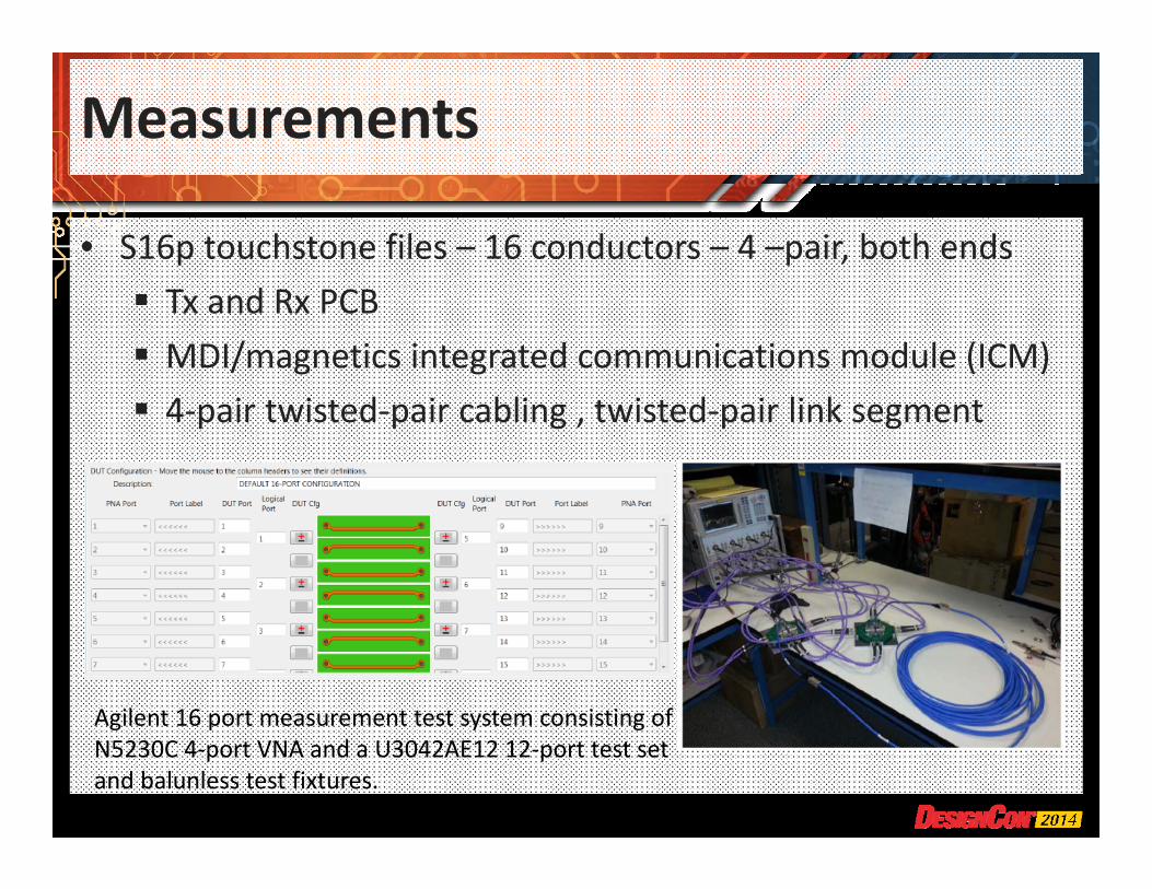
Measurements
• S16p touchstone files – 16 conductors – 4 –pair, both ends Tx and Rx PCB MDI/magnetics integrated communications module (ICM) 4‐pair twisted‐pair cabling , twisted‐pair link segment
Agilent 16 port measurement test system consisting of N5230C 4‐port VNA and a U3042AE12 12‐port test set and balunless test fixtures.

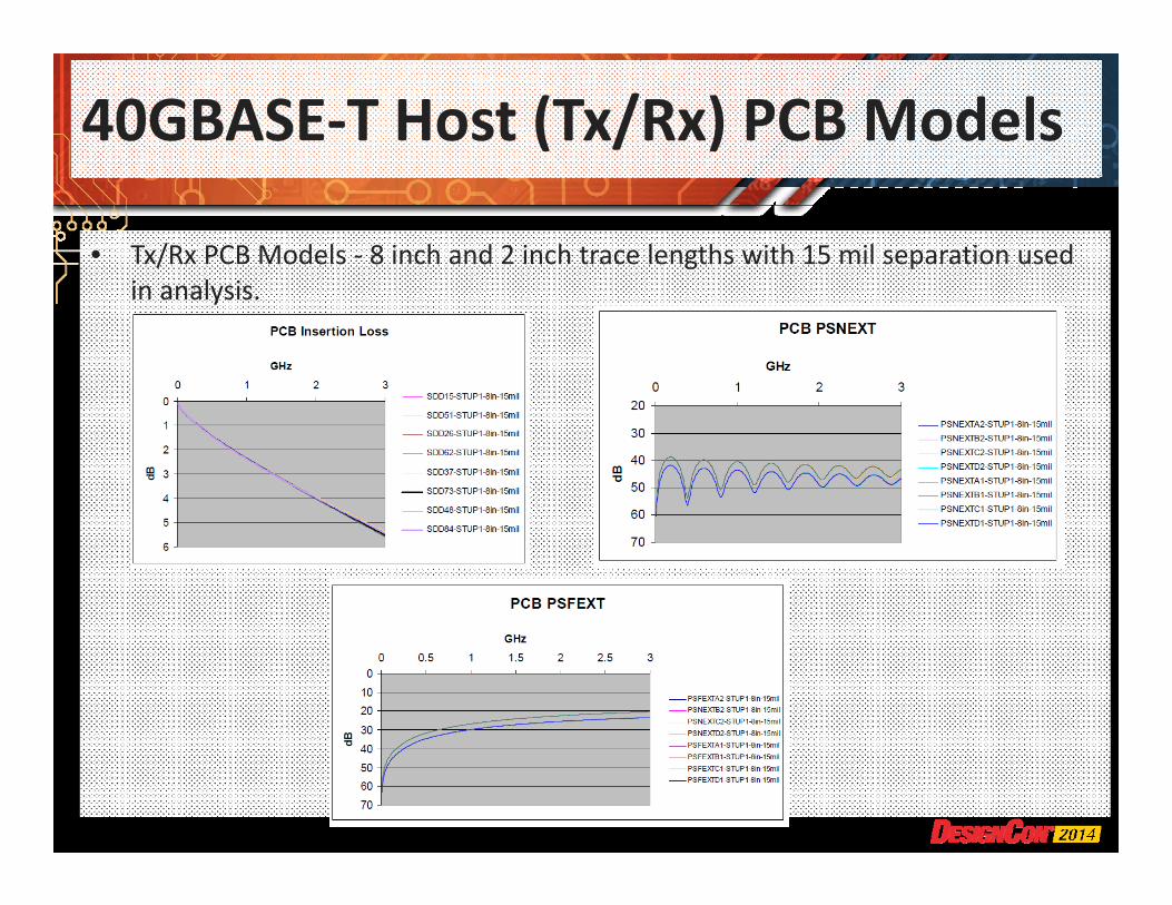
40GBASE‐T Host (Tx/Rx) PCB Models
• Touchstone files (s16p) of HFSS models of multiple variations of trace isolation for 2 inch and 8 inch trace lengths; isolation separation (s2) in Figure 2 of 15 mil, 20 mil, 25 mil and 30 mil for the 2 inch and 8 inch traces. 2 inch and 8 inch trace lengths with 15 mil separation used in analysis.
40GBASE‐T Host (Tx/Rx) PCB Models
• Tx/Rx PCB Models ‐ 8 inch and 2 inch trace lengths with 15 mil separation used in analysis.

ICM ‐ Connector and Magnetics
• Connector/magnetic measurement models

40GBASE‐T Cabling
• Alien crosstalk and mode conversion
• Alien near‐end crosstalk (ANEXT) and alien far‐end crosstalk (AFEXT) yielded responses with both a differential and common mode component.
• Shielding required to meet Category 8 alien crosstalk specifications• Shielding replaced need to specify balance parameters between
cables.

40GBASE‐T Cabling
• 40GBASE‐T Link segment and alien crosstalk

Connecting hardware
Category 6A RJ45 split pair Switched RJ45
• Cabling measurements with S‐RJ45 • Switching is implemented on insertion of the
modular plug patch cord.• S‐RJ45 plug insertion switches out the
RJ45 “split pair” where the cable pair is terminated to pins (3,6) splitting across pins (4,5).

VNA and field tester cabling measurements
• Shortest link exhibits the most allowable crosstalk and return loss noise.
• Longest link most allowable insertion loss.
WireXpert field tester with VNA adapter modules

Cabling measurements

Cabling measurements

40GBASE‐T PHY‐Channel concatenation
Concatenation: Agilent Advanced Design System (ADS) version 2013.06

Results and conclusions
• Characterization of the PHY‐Channel signal integrity performance considered for worse case PHY‐Channels.
• ICM impact considered by concatenating PHY‐Channelswith and without the ICM.
• The S‐RJ45 was introduced to support the capability of non‐magnetic operation while maintaining backward compatibility with RJ45 modular plug patch cords (i.e., backward compatibility with BASE‐T PHY’s.
• Validation of field tester capabilities to measure the installed cabling performance to support 40GBASE‐T applications.

Acknowledgements
• The authors thank Ronald Tellas, Andy Ciezak, Gina Sepic, and Paul Wachtel (Panduit)
• Arvind Patel (Psiber Data) • Bob Schaefer (Agilent) for their assistance in laboratory measurements.

DesignCon 2014
Higher Speed Ethernet: 40 Gb/s Operation Over Twisted-Pair Copper Cabling Christopher DiMinico, MC Communications [email protected] Mike Resso, Agilent [email protected] Mike Sapozhnikov, Cisco Systems [email protected] Ronald Nordin, Panduit [email protected] Harshang Pandya, Psiber Data [email protected]

Abstract The IEEE 802.3bq Task Force is chartered to extend the Ethernet protocol to operating speeds of 40 Gb/s over 4-pair balanced twisted-pair copper with a reach of up to at least 30 meters. The project was substantiated on the market need for a low cost 40 Gb/s solution backward compatible to IEEE 802.3 BASE-T family of technologies for data center applications The paper will provide a detailed technical overview of the validation of achieving 40 Gb/s over 30 meters of 4-pair balanced twisted-pair copper. The copper cabling media specifications will be explored in detail including specification development analysis and measurement methodologies to include both laboratory and field testing. In addition to the copper cabling media, the channel signal integrity performance, from transmitter-pin to receiver-pin, will be discussed including the active device transmitter and receiver printed circuit board characteristics, the transformer (magnetics), and equipment connectors.
Biographies Mike Sapozhnikov is a technical leader at Cisco Systems where he works on Catalyst 2k, 3k and 4k systems and ASIC designs. He received his B.S. in electrical engineering from SJSU. He has 17 years of experience with Signal and Power Integrity for System and ASIC level development, system design and Ethernet transceiver technology. Mike Resso is the Signal Integrity Application Scientist in the Component Test Division of Agilent Technologies and has over twenty-five years of experience in the test and measurement industry. His background includes the design and development of electro-optic test instrumentation for aerospace and commercial applications. His most recent activity has focused on the complete multiport characterization of high speed digital interconnects using Time Domain Reflectometry and Vector Network Analysis. He has authored over 30 professional publications including a book on signal integrity. Mike has been awarded one US patent and has twice received the Agilent “Spark of Insight” Award for his contribution to the company. He received a Bachelor of Science degree in Electrical and Computer Engineering from University of California. Chris Di Minico is President of MC Communications a telecommunications consulting firm and President/CTO of PHY-SI producing high speed test fixtures. Chris has over 30 years of experience in the telecommunication industry and plays an active role in the development of a number of telecommunication industry standards. Chris is an active participant and technical contributor IEEE 802.3; participating in the development of 802.3bj as the editor of clause 92 and annex 92A (100GBASE-CR4), channel definitions ad hoc co-chair in 802.3bp (reduced twisted-pair Ethernet), and cabling champion in 802.3bq (40GBASE-T). Chris was the co-chair for TIA/EIA–942 Telecommunications Infrastructure Standard for Data Centers” and is the IEEE 802.3 liaison to TIA-TR42.

Harshang Pandya is Managing Director of Singapore operation of Psiber Data, where he leads the cable certification tester product line. He has over 15 years of experience in developing test and measurement solutions. Prior to co-founding Psiber Data Singapore, he worked with Agilent Technologies in R&D and product planning roles. He received a Master of Technology in Electrical Engineering from Indian Institute of Technology (IIT) Bombay, India. Ron Nordin, Ph.D., is the Director of Research at Panduit. He received his BSEE from Purdue University in 1977, MSEE and Ph.D. EE from Northwestern University in 1979 and 1984 respectively. Current research interest include; 40/100 Gbps fiber and copper based cabling related technologies and RFID based asset tracking technologies. Prior to Panduit, he was a Distinguished Member of Technical Staff / Technical Manager at Bell Laboratories / Lucent Technologies engaged in the research and development of switching and access systems for 25 years. He is an active member of the IEEE involved in various standard developments. Ron has been awarded over 60 patents, co-authored 7 technical books and has published numerous technical papers. He also serves as an Adjunct Associate Professor of Electrical Engineering at Illinois Institute of Technology.
Introduction Approved in March 2013 the IEEE P802.3bq 40GBASE-T IEEE standards project is chartered to extend the Ethernet protocol to operating speeds of 40 Gb/s over 4-pair balanced twisted-pair copper with a reach of up to at least 30 meters. The targeted application space is within and between racks and cabinets in data centers, computer rooms, and central office environments. The 30 meter distance reach provides reasonable coverage given that data center racks and cabinet heights are typically under 2.4 m (8 ft) and racks and cabinet’s widths are nominally 1.5 meters. The 30 meter reach can support a row of 20 adjacent equipment racks or cabinets. 40GBASE-T will enable network managers to scale their networks to 40 Gigabit speeds while maintaining backward compatibility with 1000BASE-T and 10GBASE-T leveraging the cost-effectiveness and plug-and-play simplicity of copper structured cabling. Ethernet BASE-T port types support auto-negotiation allowing the transceivers to exchange capabilities and agree on the highest speed that both can support. Channel characterization is a prerequisite for evaluating signaling proposals and considering tradeoffs in silicon attributes (e.g., power, complexity) versus channel performance (e.g., insertion loss, return loss, crosstalk). To achieve a common channel reference, the P802.3bq Task Force defined a PHY-Channel as the transmission path between the transmitter and receiver blocks, the transmitter and receiver differential controlled impedance printed circuit board, the magnetics, the equipment connector (in Ethernet standards referred to as the medium dependent interface (MDI)) and 4-pair twisted-pair cabling (in Ethernet standards referred to as a twisted-pair link segment).

The paper will address the PHY-Channel signal integrity performance, from transmitter-pin to receiver-pin, including the active device transmitter and receiver printed circuit board characteristics, the transformer (magnetics), the equipment connectors (MDI’s) and the cabling twisted-pair link segment. Worse case PHY-Channels will be considered; a maximum insertion loss PHY-Channel (30 meter twisted-pair link segment) and a minimum insertion loss PHY-Channel (4 meter twisted-pair link segment). A minimum insertion loss PHY-Channel yields the worse case return loss and crosstalk. During the development of 10GBASE-T it was observed that vector network analyzer (VNA) s-parameter measurements of alien near-end crosstalk (ANEXT) and alien far-end crosstalk (AFEXT) yielded responses that included both a differential and common mode component. As 10GBASE-T specifies only differential cabling parameters, these observations led to investigations by TIA and ISO cabling standards development groups and others to further the understanding of common-to-differential mode conversion and differential-to-common mode conversion within a pair, between pairs, and between pairs in adjacent cables (e.g., cables in close proximity such as cables bundled together with tie wraps). Recognizing the need to characterize cabling and PHY-Channel common mode parameters in addition to differential mode parameters the paper will include PHY-Channel characterization as a 16 port device, 8 input ports and 8 output ports. Each element of the PHY-Channel (e.g., PCB, magnetics, equipment connector, cabling) will be either modeled or measured as a 16 port device. The cabling segments were measured by performing single-ended VNA measurements utilizing balunless test fixtures of all 8 conductors of 4-pair cabling at each end for a total of 16 conductors. The 16-port VNA measurement will enable evaluation of all possible port-to-port s-parameters (e.g., insertion loss, return loss, crosstalk and conversion loss). The measurements are to be converted to s16p Touchstone files which contain the s-parameter data in matrix format. The s16p Touchstone files are to be utilized in PHY-modeling, evaluating signaling proposals to consider tradeoffs in silicon attributes (e.g., power, complexity) versus channel performance (e.g., insertion loss, return loss, crosstalk). Field testing to assess post-installation performance of cabling is an integral component of Ethernet ecosystem. The paper will include assessment of field tester capability to measure the installed cabling performance to support 40GBASE-T applications. Field tester s-parameter measurements of the maximum insertion loss twisted-pair link segments (30 meters) and the minimum insertion loss twisted-pair link segment (4 meters) to 2 GHz are presented and compared to the VNA measurements.

40GBASE-T PHY-Channel One of the lessons learned in the development of 10GBASE-T was the need to model and characterize the channel performance from the transmitter to receiver. Recognizing this need, the 40GBASE-T Task Force initiated an ad hoc to characterize a PHY-Channel. The PHY-Channel, illustrated in Figure 1, includes the transmitter and receiver printed circuit boards (PCB), magnetics, equipment connector (MDI) and cabling (link segment). In addition to differential mode parameters the PHY-Channel is to be characterized as a 16 port device, 8 input ports and 8 output ports. Each element of the PHY-Channel (e.g., PCB, magnetics, equipment connector, cabling) will be either modeled or measured as a 16 port device. The measurements are to be converted to s16p Touchstone file which contains the s-parameter data in matrix format. The s16p Touchstone files are to be utilized in PHY-modeling, evaluating signaling proposals to consider tradeoffs in silicon attributes (e.g., power, complexity) versus channel performance (e.g., insertion loss, return loss, crosstalk).
Figure 1 – 40GBASE-T PHY-Channel
40GBASE-T Host (Tx/Rx) PCB Models For host (Tx/Rx) PCB model, Intel Corporation provided the 802.3bq Task Force s16p Touchstone files generated from HFSS PCB models representative of materials used in 2012 high volume servers. The HFSS models were validated by fabricating boards based on modeled stack-up and performing measurements. Figure 2 illustrates PCB model and Table 1 lists associated parameters. Touchstone files (s16p) were generated from HFSS models of multiple variations of trace isolation for 2 inch and 8 inch trace lengths; isolation separation (s2) in Figure 2 of 15 mil, 20 mil, 25 mil and 30 mil for the 2 inch and 8 inch traces.

Figure 2 – 40GBASE-T PCB Model
Stack-up 1 Stack-up 2
w (mils) 4 w (mils) 4 h1 (mils) 2.7 h1 (mils) 3.5 s1 (mils) 11 s1 (mils) 5.1 t1 (mils) 2 t1 (mils) 2
Dk 4.04 Dk 4.04 Df 0.02 Df 0.02
s2 (mils) varied s2 (mils) varied calculated Zdiff (ohms) 99.6 calculated Zdiff (ohms) 100.2
calculated Zcomm (ohms) 27.3 calculated Zcomm (ohms) 34.1
Table 1 – 40GBASE-T PCB Model Parameters
The insertion loss and crosstalk for stack-up 1 PCB model parameters with 8 inch trace lengths and trace separation (S2) of 15 mils are illustrated in Figures 3-5. This stack-up parameter set was used to impose a reasonable “worse case” for insertion loss and crosstalk.
PCB Insertion Loss
0
1
2
3
4
5
6
0 1 2 3
GHz
dB
SDD15-STUP1-8in-15mil
SDD51-STUP1-8in-15mil
SDD26-STUP1-8in-15mil
SDD62-STUP1-8in-15mil
SDD37-STUP1-8in-15mil
SDD73-STUP1-8in-15mil
SDD48-STUP1-8in-15mil
SDD84-STUP1-8in-15mil
Figure 3 – PCB Model Insertion Loss

The PCB PSNEXT illustrated in Figure 4 is the power summation of the three worse case NEXT disturbers (Tx) into a disturbed differential pair (Rx).
PCB PSNEXT
20
30
40
50
60
70
0 1 2 3GHz
dB
PSNEXTA2-STUP1-8in-15milPSNEXTB2-STUP1-8in-15milPSNEXTC2-STUP1-8in-15milPSNEXTD2-STUP1-8in-15milPSNEXTA1-STUP1-8in-15milPSNEXTB1-STUP1-8in-15milPSNEXTC1-STUP1-8in-15milPSNEXTD1-STUP1-8in-15mil
Figure 4 – PCB Model PSNEXT
The PCB PSFEXT illustrated in Figure 5 is the power summation of the three worse case NEXT disturbers (Tx) into a disturbed differential pair (Rx).
PCB PSFEXT
0
1020
30
40
5060
70
0 0.5 1 1.5 2 2.5 3
GHz
dB
PSFEXTA2-STUP1-8in-15milPSNEXTB2-STUP1-8in-15milPSNEXTC2-STUP1-8in-15milPSNEXTD2-STUP1-8in-15milPSFEXTA1-STUP1-8in-15milPSFEXTB1-STUP1-8in-15milPSFEXTC1-STUP1-8in-15milPSFEXTD1-STUP1-8in-15mil
Figure 5 – PCB Model PSFEXT

40GBASE-T Transformer Models For transformer models, both Bel-Fuse and Pulse provided the 802.3bq Task Force touchstone files generated from measurements. The Bel-Fuse measurement models were used, illustrated here in Figures 7-10 as the measurements include both transformer and connector in an integrated connector module (ICM) illustrated in Figure 6.
Figure 6 – ICM – connector and magnetics
ICM Insertion Loss
02468
101214
0 0.5 1 1.5 2
GHz
dB
SDD15-ICM-IL SDD51-ICM-IL SDD26-ICM-IL SDD62-ICM-IL SDD37-ICM-IL SDD73-ICM-IL SDD48-ICM-IL SDD84-ICM-IL
Figure 7 – ICM Insertion Loss

ICM Return Loss
05
10152025303540
0 0.5 1 1.5 2
GHzd
B
Category 8 - Channel RL
Category 8 ConnectingHardware RL SDD11-ICM-RL
SDD55-ICM-RL
SDD22-ICM-RL
SDD66-ICM-RL
SDD33-ICM-RL
SDD77-ICM-RL
SDD44-ICM-RL
SDD88-ICM-RL
Figure 8 – ICM Insertion Loss
The ICM PSNEXT illustrated in Figure 9 is the power summation of the three worse case NEXT disturbers (Tx) into a disturbed differential pair (Rx).
ICM PSNEXT
0102030405060708090
100110
0 0.5 1 1.5 2
GHz
dB
Category 8- ChannelPSNEXT Loss
ICM PSNEXT - RJ45 side
SDD12- NEXT
SDD13- NEXT
SDD14- NEXT
SDD23- NEXT
SDD24- NEXT
SDD34- NEXT
SDD78- NEXT
Figure 9 –ICM PSNEXT

The ICM PSFEXT illustrated in Figure 10 is the power summation of the three worse case FEXT disturbers (Tx) into a disturbed differential pair (Rx).
ICM PSFEXT
10
30
50
70
90
110
130
0 0.5 1 1.5 2
GHz
dB
CAT8 Connecting HardwarePSFEXT Loss
ICM PSFEXT
SDD52- FEXT
SDD53- FEXT
SDD54- FEXT
SDD63- FEXT
SDD64- FEXT
SDD74- FEXT
SDD16- FEXT
Figure 10 –ICM PSFEXT
40GBASE-T cabling The 40GBASE-T link segment specifications are the minimum cabling requirements specified to support operation at the objective BER. The 802.3bq Task Force established an objective to define the 40GNASE-T link segment based upon copper media specified by ISO/IEC JTC1/SC25/WG3 and TIA TR42.7 meeting the following characteristics: 4-pair, balanced twisted-pair copper cabling, up to 2 connectors, up to at least 30 m. In support of the 40GBASE-T developments, TIA TR42.7 T is developing a Standard to provide requirements for 100 Ω Category 8 balanced twisted-pair cabling and for the field test procedures used to verify the performance of installed cabling. The Standard is to be published as ANSI/TIA-568-C.2-1. In addition, TR42.7 is updating ANSI/TIA 1152 “Requirements for Field Test Instruments and Measurements for Balanced Twisted-Pair Cabling” to incorporate requirements for field testing Category 8 cabling. The Category 8 Cabling channel topology is identical to the 40GBASE-T link segment. Cabling parameters are specified within channels and between channels. The within channel specifications include insertion loss, return loss, pair-to-pair near-end crosstalk loss (NEXT), power sum NEXT loss, pair-to-pair attenuation to crosstalk ratio, far-end (ACRF), power sum ACRF, return loss, and delay. The between channel parameters are the alien crosstalk parameters, power sum alien attenuation to crosstalk ratio, far-end (PSAACRF) and power sum alien NEXT. The link segment (channel) cabling topology consisting of components (cables, cords, and connectors) is illustrated in Figure 11. The Medium dependent interfaces (MDIs) refer to eight position connectors providing the mechanical interfaces for the balanced cabling plug connectors.

Figure 11 – Twisted-pair link segment
Alien crosstalk, crosstalk coupled “between” link segments of a single disturbed link and a single disturbing link is illustrated in the schematic representation of Figure 12.
Figure 12 – Alien crosstalk
The cabling impairments of return loss (echo), NEXT and FEXT within a cable are reduced to a small residual noise utilizing cancellation methods. For 10GBASE-T, the SNR is primarily based on the ratio of the signal (insertion loss) to the alien crosstalk noise appearing at the receiver and the residual echo of the receiver.

The DesignCon 2013 paper “Mode Conversion: Missing parameters in Understanding Alien Crosstalk of LAN Cabling for Higher Speed Ethernet Sources of alien crosstalk” addressed detailing sources of alien crosstalk due to common-to-differential mode conversion and differential-to-common mode conversion within a pair, between pairs, and between pairs in adjacent cables (e.g., cables in close proximity such as cables bundled together with tie wraps). The additional sources of ANEXT due to the connecting hardware mode conversion at the near-end and the ANEXTcc between cables are illustrated in Figure 13. The subscript “c” and “d” are common and differential respectively. The directionality is left to right i.e., cd is differential-to-common mode. Referring to the legend, ANEXTcc is ANEXT common-to-common mode, NEXTdc is NEXT common-to-differential mode, TCL is transverse conversion loss and LCL is longitudinal conversion loss.
Figure 13 - Alien NEXT due to mode conversion near-end Shielding is implemented in Category 8 cable and connector designs to meet the Category 8 specifications of >60 dB powers sum alien crosstalk loss (isolation) to frequency of 2 GHz illustrated in Figure 14. The addition of the shield, providing >60 dB power sum align crosstalk loss, isolates the pairs from sources of alien crosstalk due to common-to-differential mode conversion and differential-to-common mode conversion between pairs in adjacent cables (e.g., cables in close proximity such as cables bundled together with tie wraps; see Figure 15).
Link Segment IL and Alien Crosstalk
0
20
40
60
80
100
120
0 0.5 1 1.5 2
GHz
dB
Category 8 (d0.9) ChannelPSAACRFCategory 8 (d0.9) Channel IL
Category 8 (d0.9) ChannelPSAFEXT Category 8 (d0.9) ChannelPSANEXTCategory 8 Channel (d0.9)PSAXTCategory 8 (d0.9) LinkSegment SNR
Figure 14 – Link segment IL and Alien Crosstalk
Connecting hardware at near-end of link
ANEXTcc between cables
LCL or NEXTdc of connector
TCL or NEXTcd of connector
Legend
ANEXTcc between cables
LCL or NEXTdc of connector
TCL or NEXTcd of connector
Legend
ANEXTcc between cables
LCL or NEXTdc of connector
TCL or NEXTcd of connector
Legend
IL1
IL1
DisturbingChannel
DisturbedChannel
100 DM + 50 CM termination
100 DM + 50 CM termination
IL2ILX
ILX IL2

Figure 15 – Alien crosstalk six-around-one
VNA and field tester cabling measurements VNA and field tester measurements were performed on multiple cabling test configurations with the objective of characterizing the shortest allowable link segment and the longest allowable link segment relative to the link segment limits. The near-end crosstalk and return loss noise measured at the input of a link segment due to connecting hardware at the output is reduced by the link segment insertion loss. The shortest link is chosen that exhibits the most allowable crosstalk and return loss noise relative to the limits. The longest link is chosen that exhibits the most allowable insertion loss relative to the link segment limits; see Table 2 and Figure 11 for the measured test configurations.
Set-up A B C
Category 8 0.5 m 3 m 0.5 m
Category 8 3 m 24 m 3 m
Table 2 – VNA and field tester test configurations
Six-around-one
Six disturbing
One disturbed
Six-around-one
Six disturbing
One disturbed
Six-around-one
Six disturbing
One disturbed

The VNA s-parameter cabling measurements were performed utilizing an Agilent 16 port measurement test system consisting of N5230C 4-port VNA and a U3042AE12 12-port test set and balunless test fixtures.
Figure 16 – VNA cabling measurements
The connecting hardware used in the link segment utilizes the IEC 60603-7-71 form factor with the addition of a mechanical switch (S-RJ45) to maintain backward compatibility with RJ45 modular plugs. The S-RJ45 connector fits in same faceplate footprint as the RJ45.
Figure 17 – IEC connector form factors
Shielded connector IEC 60603-7-71 form factor
Shielded Cat 6A RJ45IEC 60603-7-1 form factor
Shielded connector IEC 60603-7-71 form factor
Shielded Cat 6A RJ45IEC 60603-7-1 form factor

Switching is implemented on insertion of the modular plug patch cord; see Figure 18. The S-RJ45 plug insertion switches out the RJ45 “split pair”; see Figure 19, where the cable pair is terminated to pins (3,6) splitting across pins (4,5), with poor connector balance and conversion loss relative to the non-split pairs. Although Category 6A is specified to 500 MHz, the graph frequency range is extended to illustrate the impact of the split pair on insertion loss which would preclude the use Category 6A for applications beyond 500 MHz. In addition, the S-RJ45 modular plug patch cord and the RJ45 modular plug patch cord connector pin contacts are independent enabling S-RJ45 to support non-magnetic operation while maintaining backward compatibility with RJ45 modular plug patch cords and current BASE-T PHY’s (e.g., 10GBASE-T, 1000BASE-T) that utilize transformers.
Figure 18 – S-RJ45 compatibility to RJ45 modular plug cords
RJ45 modular plug cord
S-RJ45 modular plug cord
S-R
J45
S-R
J45
plug face
RJ45 modular plug cord
S-RJ45 modular plug cord
S-R
J45
S-R
J45
plug face

Figure 19– Category 6A RJ45 split pair insertion loss
Figure 20 illustrates the measured transverse conversion loss (TCL). The differences in magnitudes between ports (i.e., between pairs) track closely with the geometrical unbalances of the connecting hardware’s. Category 6A is specified to 500 MHz.
Figure 20 – Category 6A transverse conversion loss (TCL) – 500 MHz

Field testing to assess post-installation performance of cabling is an integral component of the Ethernet ecosystem. TR42.7 is updating ANSI/TIA 1152 “Requirements for Field Test Instruments and Measurements for Balanced Twisted-Pair Cabling” to incorporate requirements for field testing Category 8 cabling. The field testing s-parameter cabling measurements were performed utilizing the WireXpert 4500 (Psiber Data). Figure 21 illustrates the field tester connections to the link segment under test. The WireXpert field tester VNA adapter modules are utilized enabling the field tester and the VNA a common calibration reference at the end of the SMA cables attached to the test fixtures. The field tester provides integral switching. All of the link segment parameters insertion loss, return loss, and crosstalk are measured from both ends simultaneously with auto test function in less than eleven seconds without reconfiguring connections to the test fixtures.
Figure 21 – Field tester cabling measurements

Link segment insertion Loss
0
5
10
15
20
25
30
35
40
0 0.5 1 1.5 2
GHz
dB
Cat 8 - 30 m ChannelIL d0.9
VNA-Cisco-45N-0.5m-3m-0.5m
WireXpert-45N--0.5m-3m-0.5m
VNA-Panduit-45N-0.5m-3m-0.5m
VNA-Cisco-45N-3m-24m-3m
VNA-Panduit-45N-3m-24m-3m
WireXpert-45N-3m-24m-3m
Figure 22 – Link segments insertion loss
Link segment return Loss
0
10
20
30
40
50
60
70
0 0.5 1 1.5 2
GHz
dB
Cat 8 - Channel RLd0.9VNA Cisco-45N-3m-24m-3mVNA Panduit-45N-3m-24m-3mWireXpert -45N-3m-24m-3mVNA Cisco-45F-3m-24m-3mVNA Panduit-45F-3m-24m-3mWireXpert -45F-3m-24m-3m
Figure 23 – Link segment return loss (0.5m-3m-0.5m)

Link segment return Loss
0
10
20
30
40
50
60
70
80
0 0.5 1 1.5 2
GHz
dB
Cat 8 - Channel RLd0.9
WireXpert -45N-0.5m-3m-0.5m
WireXpert -45F-0.5m-3m-0.5m
VNA Panduit-45N-0.5m-3m-0.5m
VNA Panduit-45F-0.5m-3m-0.5m
VNA Cisco-45N-0.5m-3m-0.5m
VNA Cisco-45F-0.5m-3m-0.5m
Figure 24– Link segment return loss (0.5m-3m-0.5m)
The link segment PSNEXT illustrated in Figure 25 is the power summation of the three worse case NEXT disturbers (Tx) into a disturbed differential pair (Rx).
Link segment PSNEXT - 3Tx-->1Rx
0
20
40
60
80
100
120
0 0.5 1 1.5 2
GHz
dB
Cat 8-Channel PSNEXT Lossd0.9
WireXpert_45-PSNEXT-3m-24m-3m
VNA-Panduit_45-PSNEXT-3m-24m-3m
VNA-Cisco_45-PSNEXT-3m-24m-3m
Figure 25– Link segment PSNEXT (3m-24m-3m)

The link segment PSNEXT for the 0.5m-3m-0.5m illustrated in Figure 26 is the power summation of the three worse case NEXT disturbers (Tx) into a disturbed differential pair (Rx).
Link segment PSNEXT - 3Tx-->1Rx
0102030405060708090
100110
0 0.5 1 1.5 2
GHz
dB
Cat 8-Channel PSNEXTLoss d0.9
WireXpert_45-PSNEXT-0.5m-3m-0.5m
VNA-Cisco_45-PSNEXT-0.5m-3m-0.5m
VNA-Panduit_45-PSNEXT-0.5m-3m-0.5m
Figure 26 – Link segment PSNEXT (0.5m-3m-0.5m)
The link segment PSFEXT and PSACRF illustrated in Figure 27 is the power summation of the three worse case FEXT disturbers (Tx) into a disturbed differential pair (Rx).
Link segment PSFEXT-PSACRF- 3Tx--->1Rx
0
20
40
60
80
100
120
140
0 0.5 1 1.5 2
GHz
dB
VNA-Cisco-45N-ACRF
Category 8-Channel PSACRFLoss
VNA-Cisco_45-PSFEXT-3m-24m-3m
VNA-Panduit_45-PSFEXT-3m-24m-3m
WireXpert_45-PSFEXT-3m-24m-3m
WireXpert_45-PSACRF-3m-24m-3m
VNA-Panduit_45-PSACRF-3m-24m-3m
Figure 27 – Link segment PSFEXT-PSACRF (3m-24m-3m)

The link segment PSFEXT and PSACRF illustrated in Figure 28 is the power summation of the three worse case FEXT disturbers (Tx) into a disturbed differential pair (Rx).
Link segment PSFEXT-PSACRF- 3Tx-->1Rx
0102030405060708090
100
0 0.5 1 1.5 2
GHz
dB
VNA-Cisco_45-PSACRF-0.5m-3m-0.5m
WireXpert_45-PSACRF-0.5m-3m-0.5m
VNA-Panduit_45-PSACRF-0.5m-3m-0.5m
VNA-Cisco_45-PSFEXT-0.5m-3m-0.5m
VNA-Panduit_45-PSFEXT-0.5m-3m-0.5m
WireXpert_45-PSFEXT-0.5m-3m-0.5m
Category 8-Channel PSACRFLoss
Figure 28 – Link segment PSFEXT-PSACRF (0.5m-3 m-0.5m)
40GBASE-T PHY-Channel concatenation The host (Tx/Rx) PCB models, ICM measurements, and cabling measurements illustrated above are concatenated to implement a 40GBASE-T PHY-Channel. The s-parameter concatenation was performed utilizing Agilent Advanced Design System (ADS) version 2013.06. The independent s-parameter models and measurements were brought into the ADS environment and swept from 1 MHz to 5 GHz in 1MHz steps. The results were written out as single ended s16p Touchstone files. Two channels are developed, a PHY-Channel consisting of a 30 meter link segment and 8 inches of host (Tx/Rx) PCB’s (16 inches total) to allow for a “worse case” insertion loss and a short PHY-Channel with minimal insertion loss between connecting hardware to impose a “worse case” return loss and crosstalk. In addition, the ICM impact on channel performance is considered by concatenating PHY-Channels with and without the ICM. The PHY-Channels are to be utilized in PHY-modeling, evaluating signaling proposals to consider tradeoffs in silicon attributes (e.g., power, complexity) versus channel performance (e.g., insertion loss, return loss, crosstalk).

Figure 29 – PHY-Channel insertion loss (8in-3m-24m-3m-8in)
Figure 30 – PHY-Channel insertion loss (2in-0.5m-3m-0.5m-2in)

Figure 31– PHY-Channel return loss (8in-3m-24m-3m-8in)
Figure 32 – PHY-Channel return loss (2in-0.5m-3m-0.5m-2in)

Results and Conclusions The paper addressed characterization of the PHY-Channel signal integrity performance, from transmitter-pin to receiver-pin, including the active device transmitter and receiver printed circuit board characteristics, the transformer (magnetics), the equipment connectors (MDI’s) and the cabling twisted-pair link segment. Worse case PHY-Channels were considered; a maximum insertion loss PHY-Channel (30 meter twisted-pair link segment) and a minimum insertion loss PHY-Channel (4 meter twisted-pair link segment). A minimum insertion loss PHY-Channel yields the worse case return loss and crosstalk. The ICM impact on channel performance was considered by concatenating PHY-Channels with and without the ICM. The S-RJ45 was introduced to support the capability of non-magnetic operation while maintaining backward compatibility with RJ45 modular plug patch cords (i.e., backward compatibility with BASE-T PHY’s that utilize transformers) and to provide superior performance yielding significant margin from the draft Category 8 channel limits. In addition, the paper presented validation of field tester capabilities to measure the installed cabling performance to support 40GBASE-T applications. Field tester s-parameter measurements of the maximum insertion loss twisted-pair link segments (30 meters) and the minimum insertion loss twisted-pair link segment (4 meters) to 2 GHz were presented and compared to VNA measurements.
Acknowledgements The authors thank Ronald Tellas, Andy Ciezak, Gina Sepic, and Paul Wachtel (Panduit) Arvind Patel (Psiber Data) and Bob Schaefer (Agilent) for their assistance in laboratory measurements.