Embed Size (px)
Citation preview
152doi:10.1017/S1431927618001253
Microsc. Microanal. 24 (Suppl 1), 2018© Microscopy Society of America 2018
Spherical Aberration Correction for SEMs with Electrostatic-type Compact Cs-corrector Tadahiro Kawasaki1, Ryuji Yoshida1, Takeharu Kato1, Tsunenori Nomaguchi2, Shunichi Motomura2, Kenichi Nishinaka2, Toshihide Agemura2, Masahiro Tomita3, and Takashi Ikuta4
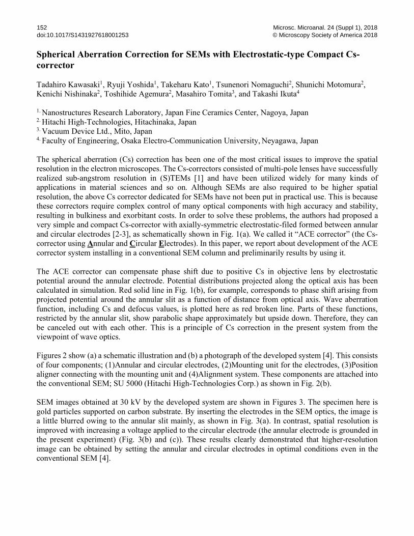
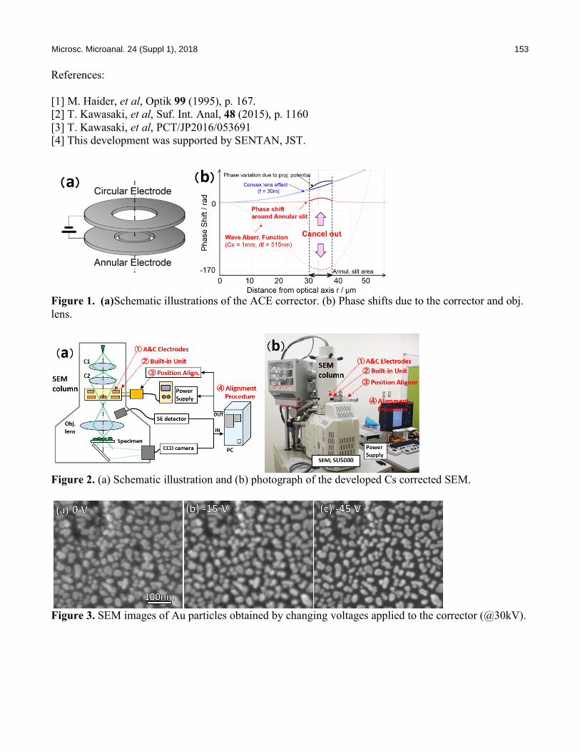
1. Nanostructures Research Laboratory, Japan Fine Ceramics Center, Nagoya, Japan 2. Hitachi High-Technologies, Hitachinaka, Japan 3. Vacuum Device Ltd., Mito, Japan 4. Faculty of Engineering, Osaka Electro-Communication University, Neyagawa, Japan The spherical aberration (Cs) correction has been one of the most critical issues to improve the spatial resolution in the electron microscopes. The Cs-correctors consisted of multi-pole lenses have successfully realized sub-angstrom resolution in (S)TEMs [1] and have been utilized widely for many kinds of applications in material sciences and so on. Although SEMs are also required to be higher spatial resolution, the above Cs corrector dedicated for SEMs have not been put in practical use. This is because these correctors require complex control of many optical components with high accuracy and stability, resulting in bulkiness and exorbitant costs. In order to solve these problems, the authors had proposed a very simple and compact Cs-corrector with axially-symmetric electrostatic-filed formed between annular and circular electrodes [2-3], as schematically shown in Fig. 1(a). We called it “ACE corrector” (the Cs-corrector using Annular and Circular Electrodes). In this paper, we report about development of the ACE corrector system installing in a conventional SEM column and preliminarily results by using it. The ACE corrector can compensate phase shift due to positive Cs in objective lens by electrostatic potential around the annular electrode. Potential distributions projected along the optical axis has been calculated in simulation. Red solid line in Fig. 1(b), for example, corresponds to phase shift arising from projected potential around the annular slit as a function of distance from optical axis. Wave aberration function, including Cs and defocus values, is plotted here as red broken line. Parts of these functions, restricted by the annular slit, show parabolic shape approximately but upside down. Therefore, they can be canceled out with each other. This is a principle of Cs correction in the present system from the viewpoint of wave optics. Figures 2 show (a) a schematic illustration and (b) a photograph of the developed system [4]. This consists of four components; (1)Annular and circular electrodes, (2)Mounting unit for the electrodes, (3)Position aligner connecting with the mounting unit and (4)Alignment system. These components are attached into the conventional SEM; SU 5000 (Hitachi High-Technologies Corp.) as shown in Fig. 2(b). SEM images obtained at 30 kV by the developed system are shown in Figures 3. The specimen here is gold particles supported on carbon substrate. By inserting the electrodes in the SEM optics, the image is a little blurred owing to the annular slit mainly, as shown in Fig. 3(a). In contrast, spatial resolution is improved with increasing a voltage applied to the circular electrode (the annular electrode is grounded in the present experiment) (Fig. 3(b) and (c)). These results clearly demonstrated that higher-resolution image can be obtained by setting the annular and circular electrodes in optimal conditions even in the conventional SEM [4].
Microsc. Microanal. 24 (Suppl 1), 2018 153
References: [1] M. Haider, et al, Optik 99 (1995), p. 167. [2] T. Kawasaki, et al, Suf. Int. Anal, 48 (2015), p. 1160 [3] T. Kawasaki, et al, PCT/JP2016/053691 [4] This development was supported by SENTAN, JST.
Figure 1. (a)Schematic illustrations of the ACE corrector. (b) Phase shifts due to the corrector and obj. lens.
Figure 2. (a) Schematic illustration and (b) photograph of the developed Cs corrected SEM.
Figure 3. SEM images of Au particles obtained by changing voltages applied to the corrector (@30kV).
(b)(a)

![Index [link.springer.com]3A978-3-642...preoperative vs. post operative aberration, 254 pseudophakic IOL, 249 selection, 250–251 shrink wrap effect, 252 spherical aberration, 249](https://img.pdfslide.net/doc/110x75/6007b3795dd77f35d01bc971/index-link-3a978-3-642-preoperative-vs-post-operative-aberration-254-pseudophakic.jpg)