Embed Size (px)
Citation preview
LX7730 rev 0.94 April 2016
© 2016 Microsemi Corporation
1
64 Analog Input RAD Tolerant Telemetry
Controller
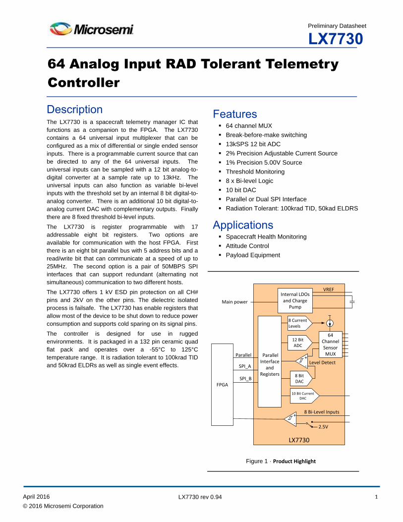
Figure 1 · Product Highlight
Preliminary Datasheet
Features 64 channel MUX
Break-before-make switching
13kSPS 12 bit ADC
2% Precision Adjustable Current Source
1% Precision 5.00V Source
Threshold Monitoring
8 x Bi-level Logic
10 bit DAC
Parallel or Dual SPI Interface
Radiation Tolerant: 100krad TID, 50kad ELDRS
Applications Spacecraft Health Monitoring
Attitude Control
Payload Equipment
Description The LX7730 is a spacecraft telemetry manager IC that
functions as a companion to the FPGA. The LX7730
contains a 64 universal input multiplexer that can be
configured as a mix of differential or single ended sensor
inputs. There is a programmable current source that can
be directed to any of the 64 universal inputs. The
universal inputs can be sampled with a 12 bit analog-to-
digital converter at a sample rate up to 13kHz. The
universal inputs can also function as variable bi-level
inputs with the threshold set by an internal 8 bit digital-to-
analog converter. There is an additional 10 bit digital-to-
analog current DAC with complementary outputs. Finally
there are 8 fixed threshold bi-level inputs.
The LX7730 is register programmable with 17
addressable eight bit registers. Two options are
available for communication with the host FPGA. First
there is an eight bit parallel bus with 5 address bits and a
read/write bit that can communicate at a speed of up to
25MHz. The second option is a pair of 50MBPS SPI
interfaces that can support redundant (alternating not
simultaneous) communication to two different hosts.
The LX7730 offers 1 kV ESD pin protection on all CH#
pins and 2kV on the other pins. The dielectric isolated
process is failsafe. The LX7730 has enable registers that
allow most of the device to be shut down to reduce power
consumption and supports cold sparing on its signal pins.
The controller is designed for use in rugged
environments. It is packaged in a 132 pin ceramic quad
flat pack and operates over a -55°C to 125°C
temperature range. It is radiation tolerant to 100krad TID
and 50krad ELDRs as well as single event effects.
LX7730
LX7730
FPGA
Parallel Interface
and Registers
Parallel
SPI_A
SPI_B
64 Channel Sensor MUX
12 Bit ADC
+
-
8 Bit DAC
Level Detect
10 Bit Current DAC
8 Bi-Level Inputs
Internal LDOs and Charge
PumpMain power
+
-2.5V
8 CurrentLevels
VREF
LX7730 rev 0.94 April 2016
© 2016 Microsemi Corporation
2
64 Analog Input RAD Tolerant Telemetry Controller
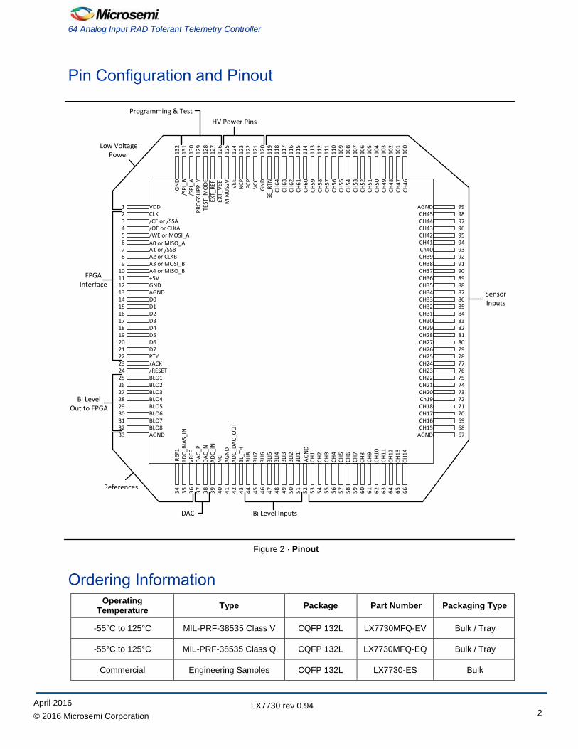
Pin Configuration and Pinout
CH41Ch40CH39CH38CH37CH36CH35CH34CH33CH32CH31CH30CH29CH28CH27CH26CH25CH24CH23CH22CH21CH20Ch19CH18CH17CH16CH15
AGND
CH
11
CH
9C
H1
0
VDD
/SP
I_A
/SP
I_B
CLK/CE or /SSA/OE or CLKA/WE or MOSI_AA0 or MISO_AA1 or /SSBA2 or CLKBA3 or MOSI_BA4 or MISO_B
D0D1D2D3D4D5D6D7
BLO1
VC
CG
ND
NC
PP
CP
VEE
CH
64
CH
63
CH
62
CH
61
CH
60
CH
59
CH
58
CH
57
CH
56
CH
55
CH
54
CH
53
CH
52
CH
51
CH
50
CH
49
CH
48
CH
47
CH
46
CH45CH44CH43CH42
BLI
8B
LI7
BLI
6B
LI5
BLI
4B
LI3
BLI
2B
LI1
DA
C_P
CH
1C
H2
CH
3C
H4
CH
5C
H6
CH
7C
H8
999897969594939291908988878685848382818079787776757473727170696867
13
21
31
13
01
29
12
81
27
12
61
25
12
41
23
12
21
21
12
01
19
11
81
17
11
61
15
11
41
13
11
21
11
11
01
09
10
81
07
10
61
05
10
41
03
10
21
01
10
0
34
35
36
37
38
39
40
41
42
43
44
45
46
47
48
49
50
51
52
53
54
55
56
57
58
59
60
61
62
63
64
65
66
123456789
101112131415161718192021222324252627282930313233
BLO2BLO3BLO4BLO5BLO6BLO7BLO8
FPGA Interface
Bi LevelOut to FPGA
References
Bi Level Inputs
Sensor Inputs
HV Power Pins
GN
D
AGND
AD
C_D
AC
_OU
T
VR
EF
DA
C_N
AD
C_B
IAS_
IN
BL_
TH
SE_R
TN
NC
AD
C_I
N
Low VoltagePower
DAC
/ACK
AGND
IREF
1
/RESET
PR
OG
SUP
PLY
TEST
_MO
DE
AG
ND
AG
ND
CH
12
CH
13
CH
14
AGND
PTY
EXT_
REF
EXT_
VEE
Programming & Test
MIN
US2
V
+5VGND
Figure 2 · Pinout
Ordering Information Operating
Temperature Type Package Part Number Packaging Type
-55°C to 125°C MIL-PRF-38535 Class V CQFP 132L LX7730MFQ-EV Bulk / Tray
-55°C to 125°C MIL-PRF-38535 Class Q CQFP 132L LX7730MFQ-EQ Bulk / Tray
Commercial Engineering Samples CQFP 132L LX7730-ES Bulk
LX7730 rev 0.94 April 2016
© 2016 Microsemi Corporation 3
Pin Description
Pin Description Pin Number Pin Designator Description
1 VDD VDD - Power reference pin – This pin is used to reference the output logic
level to the FPGA. It connects to the FPGA I/O power supply.
2 CLK
System Clock – Logic Input – This clock input is used to time synchronous
logic needed to perform the ADC conversions. There is a weak pull-down on
this pin.
3 /CE or /SSA
Chip enable or Slave Select channel A – Logic Input – Provides chip enable
for the parallel interface when /SPI_A and /SPI_B are high. Provides slave
select for the SPI channel A interface when the /SPI_A pin is pulled low. In
both cases the logic is active low. There is a weak pull-up on this pin.
4 /OE or CLKA
Output enable or SPI Clock channel A – Logic Input – Provides output
enable (read enable) for the parallel interface when /SPI_A and /SPI_B are
high. Provides the clock for the SPI channel A interface when the /SPI_A pin
is pulled low. There is a weak pull-up on this pin.
5 /WE or MOSI_A
Write enable or SPI MOSI channel A – Logic Input – Provides active low
write enable for the parallel interface when /SPI_A and /SPI_B are high.
Provides data input for the SPI channel A interface when the /SPI_A pin is
pulled low. There is a weak pull-up on this pin.
6 A0 or MISO_A
Address bit 0 or SPI MISO channel A – Logic I/O – Provides the address bit
0 (LSB) for the parallel interface when /SPI_A and /SPI_B are high.
Provides data output for the SPI channel A interface when the /SPI_A pin is
pulled low. There is a weak pull-down on this pin.
7 A1 or/SSB
Address bit 1 or Slave Select channel B – Logic Input – Provides the
address bit 1 for the parallel interface when /SPI_A and /SPI_B are high.
Provides slave select for the SPI channel B interface when the /SPI_B pin is
pulled low. There is a weak pull-up on this pin.
8 A2 or CLKB
Address bit 2 or SPI Clock channel B – Logic Input – Provides the address
bit 2 for the parallel interface when /SPI_A and /SPI_B are high. Provides
the clock for the SPI channel B interface when the /SPI_B pin is pulled low.
There is a weak pull-down on this pin.
9 A3 or MOSI_B
Address bit 3 or SPI MOSI channel B – Logic I/O – Provides the address bit
3 for the parallel interface when /SPI_A and /SPI_B are high. Provides data
input for the SPI channel B interface when the /SPI_B pin is pulled low.
There is a weak pull-down on this pin.
10 A4 or MISO_B
Address bit 4 or SPI MISO channel B – Logic I/O – Provides the address bit
4 (MSB) for the parallel interface when /SPI_A and /SPI_B are high.
Provides data output for the SPI channel B interface when the /SPI_B pin is
pulled low. There is a weak pull-down on this pin.
11 +5V
+5V power rail – Power Pin – This pin is the low voltage power rail. It is
generated internally using a linear regulator connected to the VCC rail. A
bypass capacitor to GND is required.
12, 120, 132 GND Ground – Power and Signal pin – These pins provide a return path for power
supplies and a reference point for signals.
13, 33, 41, 52,
67, 99 AGND
Analog Ground –Signal pin – These pin provides a reference point for
signals.
LX7730 rev 0.94 April 2016
© 2016 Microsemi Corporation
4
64 Analog Input RAD Tolerant Telemetry Controller
Pin Number Pin Designator Description
14-21 D#
Data I/O for the parallel interface – Logic I/O - Provides the data bits, D0
(LSB) (pin 14) through D7 (pin 21) for the parallel interface. There is a weak
pull-down on these pins.
22 PTY
Parity I/O Bit – Logic I/O – Provides the parity bit for the parallel data
communication. Even parity is used for the combination of address and data
bits and is used in both directions. There is a weak pull-down on this pin.
23 /ACK
Acknowledge Bit – Logic Output – In the event of a parity error encountered
in a serial or parallel data transfer, the /ACK pin is de-asserted (pulled high).
see “FPGA Interface” for conditions.
24 /RESET
System Reset – Logic Input– This pin provides a forced reset to the default
state of all registers and flip-flops within the LX7730. The logic is active low
which requires the pin to be pulled low to assert a reset.
25-32 BLO#
Fixed Threshold Bi Level detector output to FPGA – Logic Output– Provides
the state of the Fixed Level Bi Level Input of the same # directly to the
FPGA.
34 IREF1
Reference current programming pin –Signal Input – This pin is used to
create a precision reference current for the IC. A 20kΩ resistor should be
attached from this pin to AGND. IREF2 is an internal redundant resistor and
can be selected should IREF1 fail.
35 ADC_BIAS_IN
ADC Reference current programming pin –Signal Input – This pin is used to
create a precision reference current for the ADC. A 7.87kΩ resistor should
be attached from this pin to AGND.
36 VREF
+5V reference – Signal Output – This pin is a precision reference voltage
that can be used to provide a voltage reference to sensors for precision
measurements. A bypass capacitor to AGND is required. The internal
reference can be disabled and an external reference connected to this pin;
the internal voltage reference must be disabled in this case using the
/EXT_REF programming pin.
37,38 DAC_#
10 Bit Current DAC output – Signal Pin – This pin provides the output for the
10 bit current DAC; it should be terminated in a resistor of 1.5kΩ or less to
AGND. The DAC_P output increases with the LSB level and the DAC_N
output decrease with the LSB level. DAC_P maximum occurs at full scale
setting and DAC_N output maximum occurs at zero setting.
If the “Use DAC” bit is asserted; this implies the DAC is used to control the
current setting of the Current De-Mux. In this case the DAC_P should be left
open circuited and the DAC_N terminated to GND.
39 ADC_IN
Analog to Digital Converter Input – Signal Pin – This pin is used to monitor
the output of the anti-aliasing filters or to provide an input signal directly into
the ADC from an external source. When used as an input, the anti-aliasing
filter can be put in a Hi-Z output state.
40 NC No Connect – Test Pin – This pin is used for testing and should be left
floating in the application.
42 ADC_DAC_OUT
ADC gain scale current programming pin –Signal Input – This pin is used to
create a precision load for the current DAC portion of the SAR ADC. A 158Ω
resistor should be attached from this pin to AGND.
43 BL_TH External Bi-Level Threshold Setting – Signal Pin – This pin is used to
LX7730 rev 0.94 April 2016
© 2016 Microsemi Corporation 5
Pin Description
Pin Number Pin Designator Description
override the internal 2.5V bi-Level threshold setting and change it to the
voltage applied to this pin. An addressable register bit is used to select
either the internal or external bi-level threshold.
44-51 BLI# Fixed threshold Bi Level Signal Input – Signal Input Pin – This pin is fixed
threshold bi-level input: channel 8 (pin 44) decreasing to channel 1 (pin 51).
53-118 CH#
General purpose sensor interface – Signal I/O - This pin provides input for
the sensor interface or output for the adjustable current source. Channel 1
(pin 53) to channel 64 (pin 118). A few AGND pins are interspersed.
119 SE_RTN Single Ended Sensor Return – Signal Pin – This pin is used as a common
return for single ended sensor inputs.
121 VCC Main power supply – Power Input – This pin is the main power supply. The
internal (VEE and +5V) voltage regulators are powered from this rail.
122 PCP
Charge Pump Transfer Capacitor Positive Terminal – Power Pin – This pin is
used for the charge pump used to generate VEE; it swings between GND
and VCC. Connect a 0.47µF capacitor between this pin and the NCP pin.
123 NCP
Charge Pump Transfer Capacitor Negative Terminal – Power Pin – This pin
is used for the charge pump used to generate VEE; it swings between GND
and VEE. Connect a 0.47µF capacitor between this pin and the PCP pin.
124 VEE
Negative power rail – Power I/O – This pin is the negative voltage power rail.
It can be generated internally (using the charge pump) or supplied from an
external source connected to this pin. Use a bypass capacitor to GND. The
charge pump can be disabled by shorting the /EXT_VEE pin to GND.
125 MINUS2V
-2V Intermediate power rail – Power Pin – This pin is the low negative
voltage power rail. It is generated internally using a linear regulator
connected to the VEE rail. A bypass capacitor to GND is required.
126 /EXT_VEE
Enable external VEE – Programming pin – This pin disables the VEE charge
pump if it is shorted to ground. If high, the VEE charge pump is enabled.
There is a weak pull-up on this pin.
127 /EXT_REF
Enable External Reference – Programming pin – This pin disables the
internal voltage reference when it is shorted to ground. If high, the internally
generated voltage reference is used. There is a weak pull-up on this pin.
128 TEST_MODE Test and Trim Pins – Programming Pins - This pin is used for in package
trim and testing of the device. In normal use it should be connected to GND.
129 PROGSUPPLY
Trim Power Supply – Power Pin – This pin is used to blow fusible links when
trimming the part in package at the factory. In normal application this pin
should be shorted to +5V.
130 /SPI_A
Enable SPI Interface A – Logic Input – This pin is active low. Asserting this
pin enables the SPI channel A interface and deactivates the parallel
interface and SPI channel B. If both /SPI_A and /SPI_B pins are low, the
first asserted pin dominates. There is a weak pull-up on this pin.
131 /SPI_B
Enable SPI Interface B – Logic Input – This pin is active low. Asserting this
pin enables the SPI channel B interface and deactivates the parallel
interface and SPI channel A. If both /SPI_A and /SPI_B pins are low, the
first asserted pin dominates. There is a weak pull-up on this pin.
LX7730 rev 0.94 April 2016
© 2016 Microsemi Corporation
6
64 Analog Input RAD Tolerant Telemetry Controller
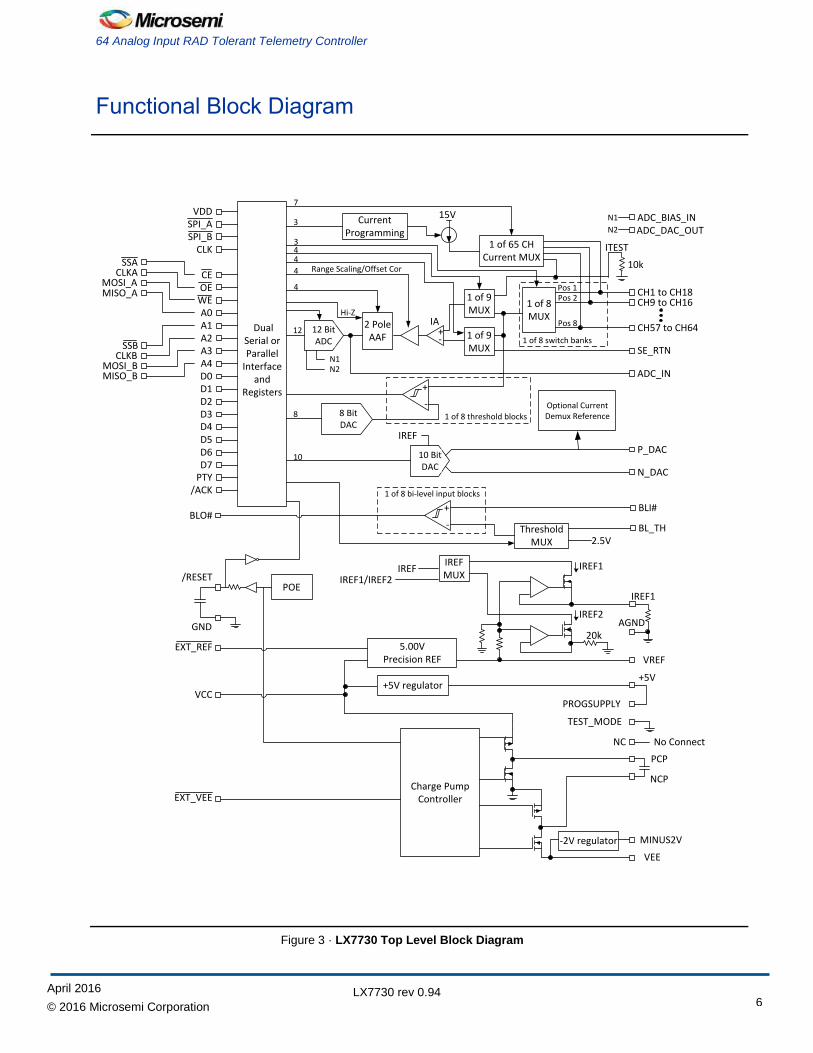
Functional Block Diagram
1 of 8 threshold blocks
1 of 8 bi-level input blocks
BLI#
2.5V
D0D1D2D3
Dual Serial or Parallel
Interfaceand
Registers
BLO#
15V
+-
12 Bit ADC
Current Programming
1 of 65 CH Current MUX
+
- 8 Bit DAC
VDD
1 of 9 MUX
1 of 9 MUX
1 of 8 MUX
10 Bit DAC
IREFD4D5D6D7
N_DAC
1 of 8 switch banks
CE
A1A2A3A4
WEOE
A0
CLKBMOSI_B
SSB
CLKASSA
MOSI_A
MISO_B
MISO_A
SPI_BSPI_A
CLK
2 Pole AAF
CH1 to CH18
CH57 to CH64
SE_RTN
P_DAC
+
- Threshold MUX
BL_TH
ADC_IN
IA
Range Scaling/Offset Cor
Hi-Z
PTY
7
3
344
4
4
12
8
10
ITEST
/ACK
CH9 to CH16
Pos 1Pos 2
Pos 8
VCC
PCP
NCP
VEE
+5V regulator+5V
5.00V Precision REF VREF
IREF2
IREF1
IREF1
IREFMUX
IREF
EXT_REF
IREF1/IREF2
Charge PumpControllerEXT_VEE
-2V regulator MINUS2V
AGNDGND
Optional Current Demux Reference
20k
N1N2
N1
N2
ADC_BIAS_INADC_DAC_OUT
10k
POE/RESET
PROGSUPPLY
TEST_MODE
NC No Connect
Figure 3 · LX7730 Top Level Block Diagram
LX7730 rev 0.94 April 2016
© 2016 Microsemi Corporation 7
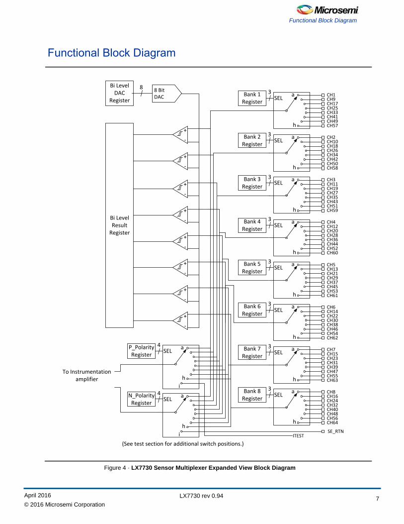
Functional Block Diagram
Functional Block Diagram
8 Bit DAC
8a
h
SEL
+
-
+
-
+
-
Bi Level Result
Register
Bi LevelDAC
RegisterBank 1
Register
a
h
SELBank 2
Register
a
h
SELBank 3
Register
a
h
SELBank 4
Register
a
h
SELBank 5
Register
a
h
SELBank 6
Register
a
h
SELBank 7
Register
a
h
SELBank 8
Register
a
h
SELP_PolarityRegister
a
h
SELN_Polarity
Register
+
-
+
-
+
-
+
-
+
-
To Instrumentation amplifier
3
3
3
3
3
3
3
3
4
4
iSE_RTN
(See test section for additional switch positions.)
i
ITEST
CH1CH9CH17CH25CH33CH41CH49CH57
CH2CH10CH18CH26CH34CH42CH50CH58
CH3CH11CH19CH27CH35CH43CH51CH59
CH4CH12CH20CH28CH36CH44CH52CH60
CH5CH13CH21CH29CH37CH45CH53CH61
CH6CH14CH22CH30CH38CH46CH54CH62
CH7CH15CH23CH31CH39CH47CH55CH63
CH8CH16CH24CH32CH40CH48CH56CH64
Figure 4 · LX7730 Sensor Multiplexer Expanded View Block Diagram
LX7730 rev 0.94 April 2016
© 2016 Microsemi Corporation
8
64 Analog Input RAD Tolerant Telemetry Controller
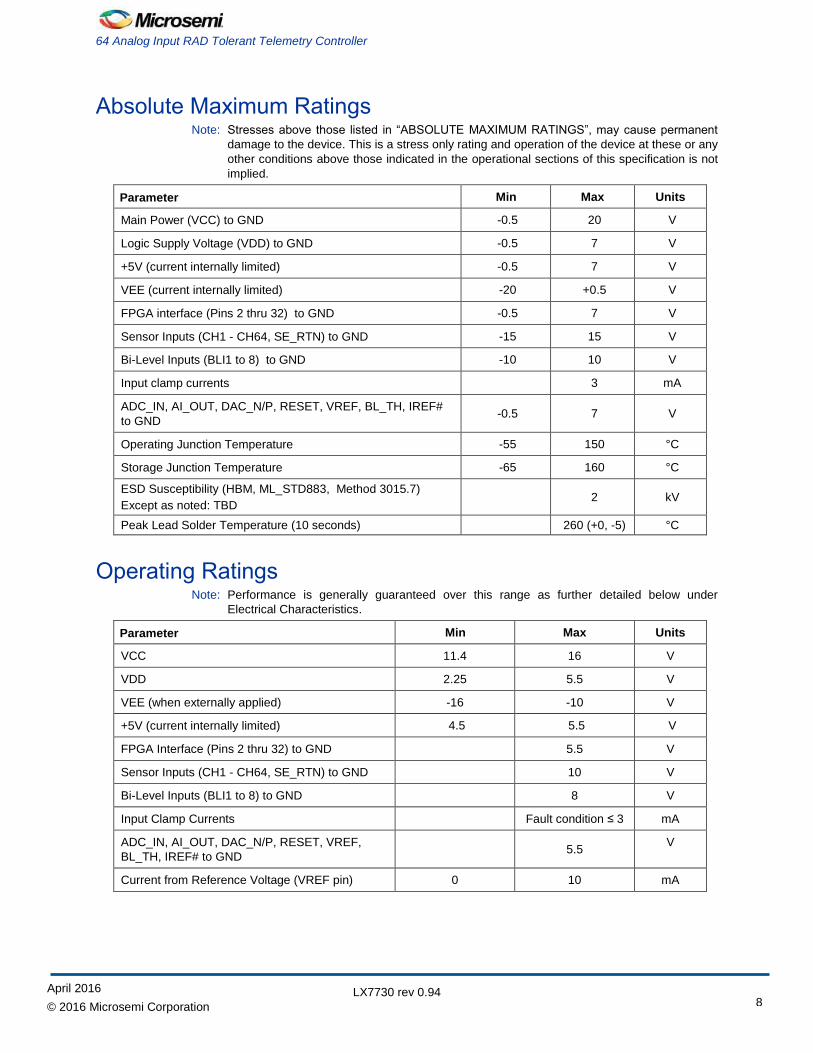
Absolute Maximum Ratings Note: Stresses above those listed in “ABSOLUTE MAXIMUM RATINGS”, may cause permanent
damage to the device. This is a stress only rating and operation of the device at these or any
other conditions above those indicated in the operational sections of this specification is not
implied.
Parameter Min Max Units
Main Power (VCC) to GND -0.5 20 V
Logic Supply Voltage (VDD) to GND -0.5 7 V
+5V (current internally limited) -0.5 7 V
VEE (current internally limited) -20 +0.5 V
FPGA interface (Pins 2 thru 32) to GND -0.5 7 V
Sensor Inputs (CH1 - CH64, SE_RTN) to GND -15 15 V
Bi-Level Inputs (BLI1 to 8) to GND -10 10 V
Input clamp currents 3 mA
ADC_IN, AI_OUT, DAC_N/P, RESET, VREF, BL_TH, IREF#
to GND -0.5 7 V
Operating Junction Temperature -55 150 °C
Storage Junction Temperature -65 160 °C
ESD Susceptibility (HBM, ML_STD883, Method 3015.7)
Except as noted: TBD 2 kV
Peak Lead Solder Temperature (10 seconds) 260 (+0, -5) °C
Operating Ratings Note: Performance is generally guaranteed over this range as further detailed below under
Electrical Characteristics.
Parameter Min Max Units
VCC 11.4 16 V
VDD 2.25 5.5 V
VEE (when externally applied) -16 -10 V
+5V (current internally limited) 4.5 5.5 V
FPGA Interface (Pins 2 thru 32) to GND 5.5 V
Sensor Inputs (CH1 - CH64, SE_RTN) to GND 10 V
Bi-Level Inputs (BLI1 to 8) to GND 8 V
Input Clamp Currents Fault condition ≤ 3 mA
ADC_IN, AI_OUT, DAC_N/P, RESET, VREF,
BL_TH, IREF# to GND
5.5
V
Current from Reference Voltage (VREF pin) 0 10 mA
LX7730 rev 0.94 April 2016
© 2016 Microsemi Corporation 9
Thermal Properties
Thermal Properties
Thermal Resistance Typ Units
θJC 2 °C/W
Note: The JA numbers assume no forced airflow. Junction Temperature is calculated using TJ = TA + (PD x JA). In
particular, θJA is a function of the PCB construction. The stated number above is for a four-layer board in
accordance with JESD-51 (JEDEC).
Electrical Characteristics The following specifications apply over the operating ambient temperature of -55C ≤ TA ≤ 125C except where
otherwise noted with the following test conditions: VCC = 15V, VDD = 3.3V; RIREF = 20kΩ; RADC_BIAS_IN = 7.87kΩ;
RADC_DAC_OUT = 158Ω; / EXT_VEE open, /EXT_REF open. CH1 and CH2 selected and CH2 grounded. CLK =
500kHz. Reg 7 =001010xx. Typical parameter refers to TJ = 25°C. Positive currents flow into the pin.
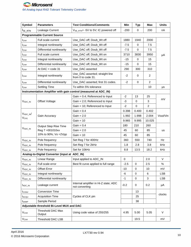
Symbol Parameters Test Conditions/Comments Min Typ Max Units
Operating Current
IVCC VCC Normal Current 55 70 85 mA
IVCC VCC Standby Current Chip Enable Register de-asserted 2.0 4.0 7.0 mA
IVEE VEE Current Using external VEE source. Positive
current out of pin. -3.5 -4.7 -6.0 mA
Under Voltage Detection
VVCC VCC UVLO Voltage rising; 200mV Hysteresis 9.5 10 10.5 V
VVEE VEE UVLO Voltage falling; 200mV Hysteresis -8.2 -8.0 -7.8 V
V+5V +5V UVLO Voltage rising; 200mV Hysteresis 3.9 4.15 4.4 V
Internally Regulated Voltages and Currents
VVEE VEE voltage VCC - |VEE| 2.0 2.6 2.9 V
V+5V_NOM +5V voltage 4.8 5.00 5.20 V
VREF_NOM VREF voltage 4.95 5.00 5.05 V
VIREF IREF pin voltage RIREF = 20kΩ 1.568 1.600 1.632 V
Analog MUX
VCH# Differential Range CH# to CH# or CH# to SE_RTN 0 5 V
VCH1 &
VCH2 Common Mode Range With VCH1 –VCH2 = 5V -5 5 V
VCH# Voltage Clamp
(power applied)
Clamp Current = 1mA (into pin) (1)
15 16 17 V
Clamp Current = 1mA (out of pin) -23 -20 -17
VCH# Voltage Clamp
(VCC=VEE=0)
Clamp Current = 1mA (into pin) 17 20 23 V
Clamp Current = 1mA (out of pin) -23 -20 -17
All to VCH1 Ch – Ch Isolation
CH1 and SE_RTN selected; CH2 to
CH64 each with series 2kΩ to a
10kHz common source, CH1 with
2kΩ to GND. SE_RTN to GND.
60 dB
VADC_IN Settling Time Including dead time 10 µs
ICH# Bias Current VCH1= -5V to 5V -200 0 200 nA
ICH# Leakage Current VCH1= -5V to 5V; IC powered off -200 0 200 nA
ISE_RTN Bias Current VSE_RTN= -5V to 5V -200 0 200 nA
LX7730 rev 0.94 April 2016
© 2016 Microsemi Corporation
10
64 Analog Input RAD Tolerant Telemetry Controller
Symbol Parameters Test Conditions/Comments Min Typ Max Units
ISE_RTN Leakage Current VSE_RTN= -5V to 5V; IC powered off -200 0 200 nA
Programmable Current Source
ICH# Full scale current Use_DAC off; Doub_Wt off 1880 1940 2000
µA
ICH# Integral nonlinearity Use_DAC off; Doub_Wt off -7.5 0 7.5
ICH# Differential nonlinearity Use_DAC off; Doub_Wt off -7.5 0 7.5
ICH# Full scale current Use_DAC off; Doub_Wt on 3710 3830 3950
ICH# Integral nonlinearity Use_DAC off; Doub_Wt on -15 0 15
ICH# Differential nonlinearity Use_DAC off; Doub_Wt on -15 0 15
ICH# At DAC = code 31 Use_DAC asserted 290 300 310
ICH# Integral nonlinearity Use_DAC asserted; straight line
from 0 to code 31. -2 0 2
ICH# Differential nonlinearity Use_DAC asserted; first 31 codes. -2 0 2
ICH# Settling Time To within 5% tolerance 10 µs
Instrumentation Amplifier with gain control (measured at ADC_IN)
VADC_IN Offset Voltage
Gain = 0.4; Referenced to Input -2 13 25 mV
Gain = 2.0; Referenced to Input -3 0 3
Gain = 10; Referenced to Input -2 0 2
VADC_IN/
VCH1 Gain Accuracy
Gain = 0.4 0.398 0.400 0.402
Vout/Vin Gain = 2.0 1.992 1.998 2.004
Gain = 10 9.965 9.995 10.025
VADC_IN
Output Step Rise Time
Reg 7 =001010xx
10% to 90%; Vo =2Vpp
Gain = 0.4 180 210 260
us Gain = 2.0 45 60 85
Gain = 10 45 60 85
VADC_IN Pole frequency Set Reg 7 for 400Hz 360 550 740 Hz
VADC_IN Pole frequency Set Reg 7 for 2kHz 1.8 2.8 3.8 kHz
VADC_IN Pole frequency Set for 10kHz 8.8 13.5 18.2 kHz
Analog-to-Digital Converter (input at ADC_IN)
VADC_IN Linear Range Input applied to ADC_IN 0 2.0 V
VADC_IN Full scale error Best fit curve applied to full range -2.5 0 2.5 %
VADC_IN Offset Error
-10 0 10 mV
VADC_IN Integral nonlinearity -6 0 6 LSB
VADC_IN Differential nonlinearity -1 0 3 LSB
IADC_IN Leakage current Internal amplifier in Hi-Z state; ADC
not converting -0.2 0 0.2 µA
tCONV Conversion Time
Cycles of CLK pin
13 clocks
tACQU Acquisition Time 25
tSAMP Sample Period 38
Adjustable threshold Bi-Level MUX and DAC
VCH# Threshold DAC Max
Output Using code value of 255/255 4.95 5.00 5.05 V
VCH# Threshold DAC LSB 19.5 mV

LX7730 rev 0.94 April 2016
© 2016 Microsemi Corporation 11
Electrical Characteristics
Symbol Parameters Test Conditions/Comments Min Typ Max Units
Weight
VCH# DAC Integral Linearity Using codes 20 to 240, best fit
straight line
-1 1 LSB
VCH# Offset error -10 10 mV
VCH# DAC Differential Linearity -0.75 0.75 LSB
VCH# Hysteresis Rising threshold = DAC output;
falling threshold has hysteresis 75 112 150 mV
10 Bit Current DAC
IDAC_P Full scale -2.06 -2.00 -1.94 mA
IDAC_N Full scale 0 mA
IDAC_P,N LSB Weight -1.953 µA
IDAC_ P,N Integral Nonlinearity -5 0 5 LSB
IDAC_ P,N Differential Nonlinearity -0.5 0 0.5 LSB
VDAC_ P,N Compliance Range 0 3 V
IDAC_ P,N Settling 0.2 1 µs
Fixed Threshold Bi-Level Inputs
VBLI# Threshold
(Rising Voltage)
Internal reference 2.45 2.50 2.55 V
With external 2.50V reference 2.45 2.50 2.55
VBLI# Hysteresis Only falling threshold has hysteresis;
Rising is dead on 60 120 180 mV
VBLI# Voltage Clamp
(power applied)
Clamp Current = 1mA (into pin) 15 20 23 V
Clamp Current = 1mA (out of pin) -23 -20 -15
VBLI# Voltage Clamp
(power removed)
Clamp Current = 1mA (into pin) 15 20 23 V
Clamp Current = 1mA (out of pin) -23 -20 -15
IBLI# Bias Current VBLI1 = 0V to 5V -0.2 0 1.5 µA
IBLI# Leakage Current VBLI1 = 0V to 5V; IC powered off -0.2 0 1.5 µA
tBLI# Propagation Delay High to low transition 0.3 0.8 1.3
µs Low to high transition 0.8 2.1 3.4
VBL_TH Ext Threshold Pin Range 0.1 4.9 V
IBL_TH Threshold Pin Leakage VBL_TH = 0V to 5V -0.2 0 2.0 µA
LX7730 rev 0.94 April 2016
© 2016 Microsemi Corporation
12
64 Analog Input RAD Tolerant Telemetry Controller
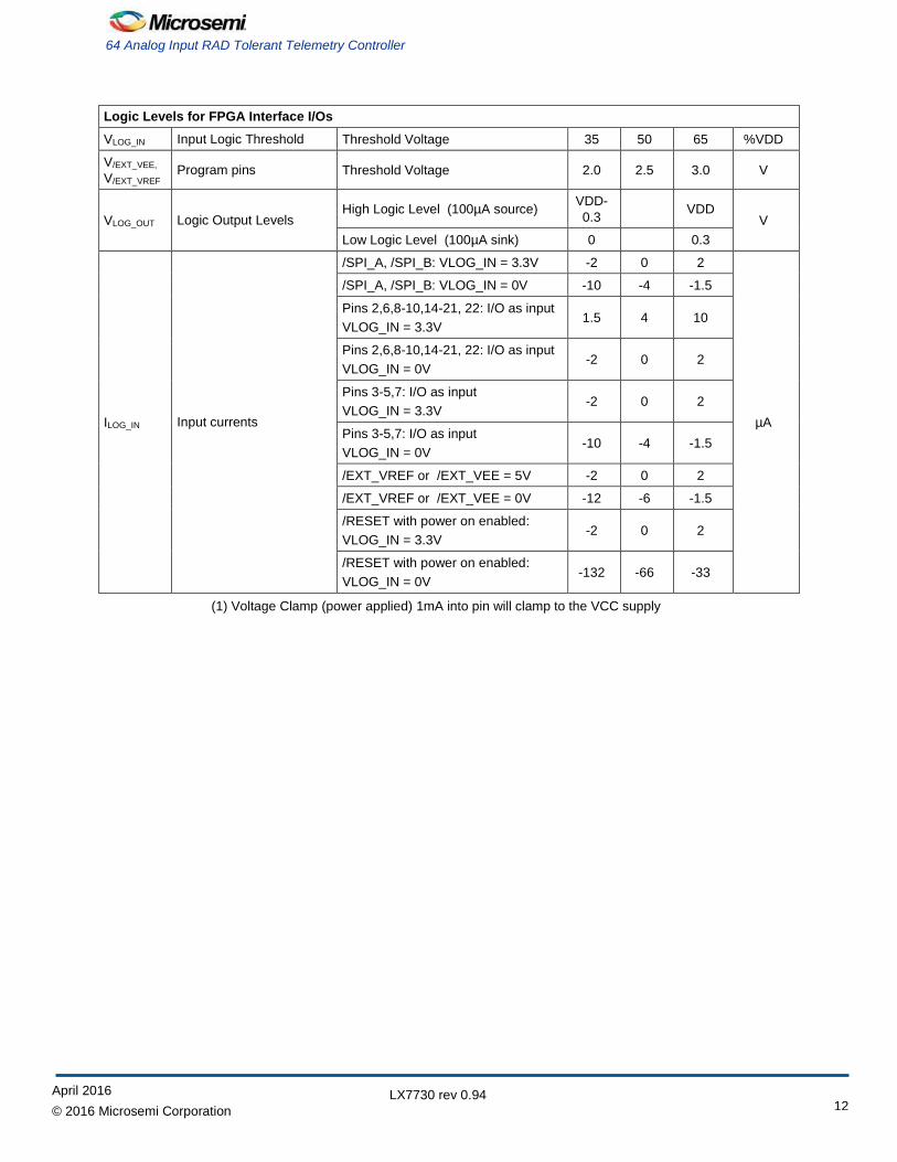
Logic Levels for FPGA Interface I/Os
VLOG_IN Input Logic Threshold Threshold Voltage 35 50 65 %VDD
V/EXT_VEE,
V/EXT_VREF Program pins Threshold Voltage 2.0 2.5 3.0 V
VLOG_OUT Logic Output Levels High Logic Level (100µA source)
VDD-
0.3 VDD
V
Low Logic Level (100µA sink) 0 0.3
ILOG_IN Input currents
/SPI_A, /SPI_B: VLOG_IN = 3.3V -2 0 2
µA
/SPI_A, /SPI_B: VLOG_IN = 0V -10 -4 -1.5
Pins 2,6,8-10,14-21, 22: I/O as input
VLOG_IN = 3.3V 1.5 4 10
Pins 2,6,8-10,14-21, 22: I/O as input
VLOG_IN = 0V -2 0 2
Pins 3-5,7: I/O as input
VLOG_IN = 3.3V -2 0 2
Pins 3-5,7: I/O as input
VLOG_IN = 0V -10 -4 -1.5
/EXT_VREF or /EXT_VEE = 5V -2 0 2
/EXT_VREF or /EXT_VEE = 0V -12 -6 -1.5
/RESET with power on enabled:
VLOG_IN = 3.3V -2 0 2
/RESET with power on enabled:
VLOG_IN = 0V -132 -66 -33
(1) Voltage Clamp (power applied) 1mA into pin will clamp to the VCC supply
LX7730 rev 0.94 April 2016
© 2016 Microsemi Corporation 13
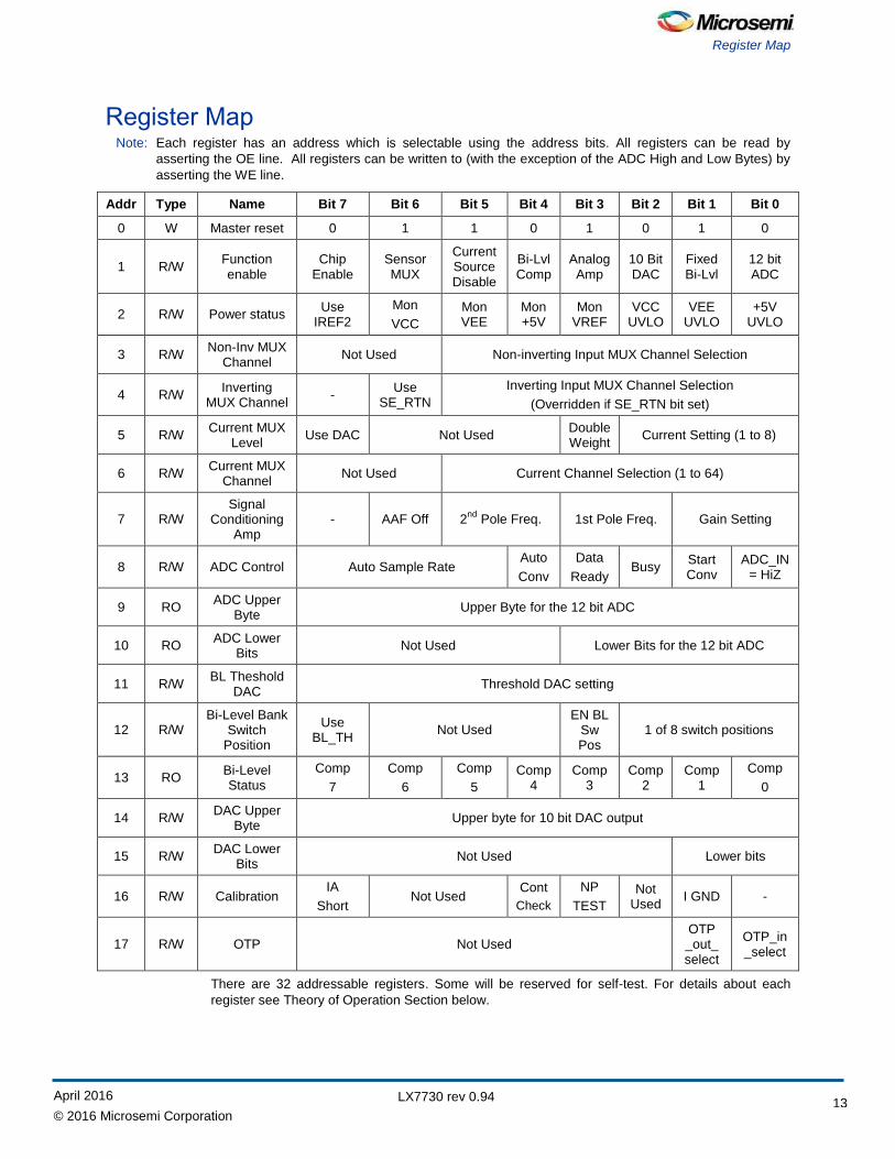
Register Map
Register Map Note: Each register has an address which is selectable using the address bits. All registers can be read by
asserting the OE line. All registers can be written to (with the exception of the ADC High and Low Bytes) by
asserting the WE line.
Addr Type Name Bit 7 Bit 6 Bit 5 Bit 4 Bit 3 Bit 2 Bit 1 Bit 0
0 W Master reset 0 1 1 0 1 0 1 0
1 R/W Function enable
Chip Enable
Sensor MUX
Current Source Disable
Bi-Lvl Comp
Analog Amp
10 Bit DAC
Fixed Bi-Lvl
12 bit ADC
2 R/W Power status Use
IREF2
Mon
VCC
Mon VEE
Mon +5V
Mon VREF
VCC UVLO
VEE UVLO
+5V UVLO
3 R/W Non-Inv MUX
Channel Not Used Non-inverting Input MUX Channel Selection
4 R/W Inverting
MUX Channel -
Use SE_RTN
Inverting Input MUX Channel Selection
(Overridden if SE_RTN bit set)
5 R/W Current MUX
Level Use DAC Not Used
Double Weight
Current Setting (1 to 8)
6 R/W Current MUX
Channel Not Used Current Channel Selection (1 to 64)
7 R/W Signal
Conditioning Amp
- AAF Off 2nd
Pole Freq. 1st Pole Freq. Gain Setting
8 R/W ADC Control Auto Sample Rate Auto
Conv
Data
Ready Busy
Start Conv
ADC_IN = HiZ
9 RO ADC Upper
Byte Upper Byte for the 12 bit ADC
10 RO ADC Lower
Bits Not Used Lower Bits for the 12 bit ADC
11 R/W BL Theshold
DAC Threshold DAC setting
12 R/W Bi-Level Bank
Switch Position
Use BL_TH
Not Used EN BL
Sw Pos
1 of 8 switch positions
13 RO Bi-Level Status
Comp
7
Comp
6
Comp
5
Comp4
Comp 3
Comp 2
Comp 1
Comp
0
14 R/W DAC Upper
Byte Upper byte for 10 bit DAC output
15 R/W DAC Lower
Bits Not Used Lower bits
16 R/W Calibration IA
Short Not Used
Cont
Check
NP
TEST
Not Used
I GND -
17 R/W OTP Not Used OTP _out_ select
OTP_in_select
There are 32 addressable registers. Some will be reserved for self-test. For details about each
register see Theory of Operation Section below.
LX7730 rev 0.94 April 2016
© 2016 Microsemi Corporation
14
64 Analog Input RAD Tolerant Telemetry Controller
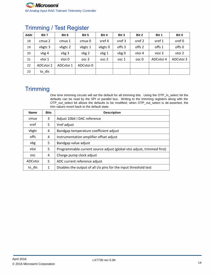
Trimming / Test Register Addr Bit 7 Bit 6 Bit 5 Bit 4 Bit 3 Bit 2 Bit 1 Bit 0
18 cmux 2 cmux 1 cmux 0 vref 4 vref 3 vref 2 vref 1 vref 0
19 vbgtc 3 vbgtc 2 vbgtc 1 vbgtc 0 offs 3 offs 2 offs 1 offs 0
20 vbg 4 vbg 3 vbg 2 vbg 1 vbg 0 vtoi 4 vtoi 3 vtoi 2
21 vtoi 1 vtoi 0 osc 3 osc 2 osc 1 osc 0 ADCvtoi 4 ADCvtoi 3
22 ADCvtoi 2 ADCvtoi 1 ADCvtoi 0
23 Io_dis
Trimming One time trimming circuits will set the default for all trimming bits. Using the OTP_in_select bit the
defaults can be read by the SPI or parallel bus. Writing to the trimming registers along with the
OTP_out_select bit allows the defaults to be modified; when OTP_out_select is de-asserted, the
trim values revert back to the default state.
Name Bits Description
cmux 3 Adjust 10bit I DAC reference
vref 5 Vref adjust
vbgtc 4 Bandgap temperature coefficient adjust
offs 4 Instrumentation amplifier offset adjust
vbg 5 Bandgap value adjust
vtoi 5 Programmable current source adjust (global vtoi adjust, trimmed first)
osc 4 Charge pump clock adjust
ADCvtoi 5 ADC current reference adjust
Io_dis 1 Disables the output of all i/o pins for the input threshold test
LX7730 rev 0.94 April 2016
© 2016 Microsemi Corporation 15
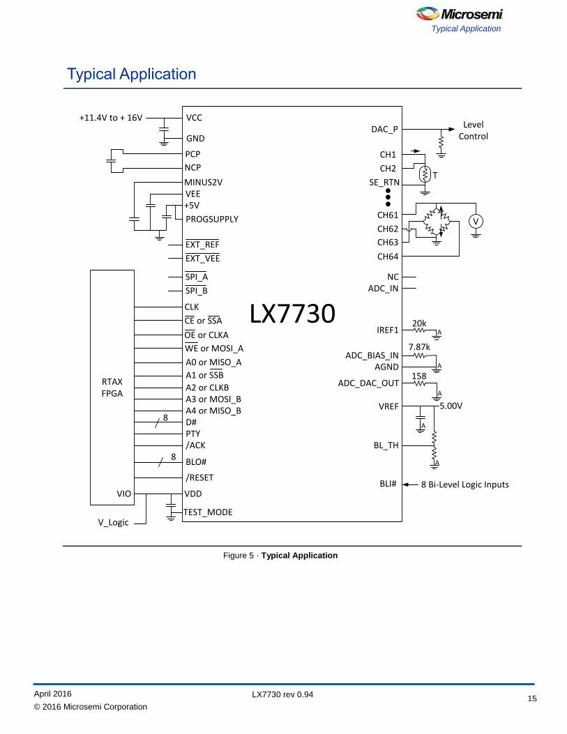
Typical Application
Typical Application
RTAXFPGA
LX7730WE or MOSI_A
OE or CLKA
A0 or MISO_A
D#
DAC_P
VREF 5.00V
8 Bi-Level Logic InputsBLI#
IREF1
BLO#8
CH1
CH2
SE_RTN
CH61
CH62
VDDVIO
V_Logic
+11.4V to + 16V
GND
VEE
VCC
+5V
PCP
NCPT
CH63
8
CH64
V
Level Control
CE or SSA
SPI_A
SPI_B
CLK
A1 or SSB
A2 or CLKBA3 or MOSI_BA4 or MISO_B
ADC_BIAS_IN
20k
PTYBL_TH
NCADC_IN
/ACK
/RESET
EXT_REF
EXT_VEE
MINUS2V
AGND A
A
A
A
7.87k
ADC_DAC_OUTA
158
TEST_MODE
PROGSUPPLY
Figure 5 · Typical Application
LX7730 rev 0.94 April 2016
© 2016 Microsemi Corporation
16
64 Analog Input RAD Tolerant Telemetry Controller
Theory of Operation
Analog Multiplexer
The analog multiplexer (AMUX) consists of 64 inputs. There are two outputs which are the non-
inverting and inverting inputs of the following instrumentation amplifier stage. Since the ADC
processes only positive voltages, the input voltage at the non-inverting channel is expected to be
greater than or equal to the inverting channel. The AMUX is physically divided into eight banks of
eight inputs. Only one CH#, from one input bank can be selected at a time which means that
differential measurements must consist of two CH#s from two different input banks. For a single
ended input measurement the common SE_RTN reference pin can be selected by asserting the
appropriate bit in the inverting terminal AMUX register. The EN_BL SW POS bit of register 12 must
be de-asserted to use the analog multiplexing registers (3 and 4). The address bits for the Analog
MUX (registers 3 and 4) are shown in the table below.
Bi-Level Inputs with Adjustable Threshold
The 64 sensor inputs can also be used as bi-level detection inputs. The bi-level detection
comparators monitor one position, simultaneously, from each of the input banks; the position is
register selectable. The Bi-level MUX and the AMUX are not independent, the EN_BL SW POS bit
of register 12 must be asserted to use the Bi-Level MUX. The selected eight bi-level inputs are
compared to a common adjustable threshold that is developed using an 8 bit binary DAC. The
outputs for the group of 8 are available in a register that is continuously updated and can be polled
to monitor the status. The comparators are sampled during the clock cycle that the Bi-Level Status
is read.
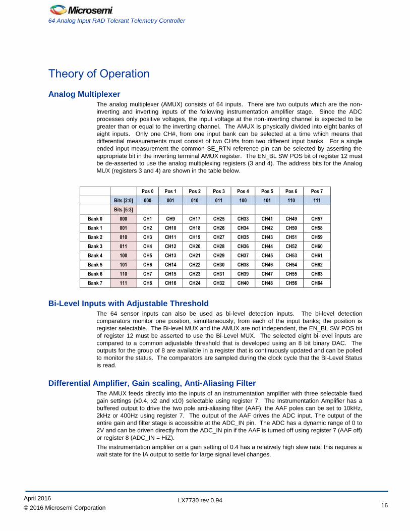
Differential Amplifier, Gain scaling, Anti-Aliasing Filter
The AMUX feeds directly into the inputs of an instrumentation amplifier with three selectable fixed
gain settings (x0.4, x2 and x10) selectable using register 7. The Instrumentation Amplifier has a
buffered output to drive the two pole anti-aliasing filter (AAF); the AAF poles can be set to 10kHz,
2kHz or 400Hz using register 7. The output of the AAF drives the ADC input. The output of the
entire gain and filter stage is accessible at the ADC_IN pin. The ADC has a dynamic range of 0 to
2V and can be driven directly from the ADC_IN pin if the AAF is turned off using register 7 (AAF off)
or register 8 (ADC_IN = HiZ).
The instrumentation amplifier on a gain setting of 0.4 has a relatively high slew rate; this requires a
wait state for the IA output to settle for large signal level changes.
Pos 0 Pos 1 Pos 2 Pos 3 Pos 4 Pos 5 Pos 6 Pos 7
Bits [2:0] 000 001 010 011 100 101 110 111
Bits [5:3]
Bank 0 000 CH1 CH9 CH17 CH25 CH33 CH41 CH49 CH57
Bank 1 001 CH2 CH10 CH18 CH26 CH34 CH42 CH50 CH58
Bank 2 010 CH3 CH11 CH19 CH27 CH35 CH43 CH51 CH59
Bank 3 011 CH4 CH12 CH20 CH28 CH36 CH44 CH52 CH60
Bank 4 100 CH5 CH13 CH21 CH29 CH37 CH45 CH53 CH61
Bank 5 101 CH6 CH14 CH22 CH30 CH38 CH46 CH54 CH62
Bank 6 110 CH7 CH15 CH23 CH31 CH39 CH47 CH55 CH63
Bank 7 111 CH8 CH16 CH24 CH32 CH40 CH48 CH56 CH64
LX7730 rev 0.94 April 2016
© 2016 Microsemi Corporation 17
Theory of Operation
+
-AMUX
BufferI/A
AAF
12 Bit ADC
ADC_IN
Register 1: Analog Amp
Enable
Register 7: Filter Off
Disable
Register 1: 12 bit ADC
Enable
Register 7: Gain Setting
Register 7: Pole Freq
Register 9 & 10: ADC Output
Register 8: ADC Control
The table below indicates how to configure the amplifier and filter chain for various modes of operation.
Condition 12 bit ADC Analog Amp AAF off
Use entire chain: IA, buffer, AAF and ADC on on on
Use ADC driven by ADC_IN on Don’t care off
Shut everything off to save maximum power off off off
12 Bit ADC
The ADC uses a successive approximation register (SAR) design. The CLK input sequences the
ADC logic.
The ADC can be set to convert continuously or to convert on request using START CONVERT.
Whenever a conversion is in process the BUSY status bit is asserted. When the conversion is
complete the DATA READY bit is set. The ADC value registers are updated when the DATA
READY bit is asserted, but will not change during the process of a data read which starts by
reading the upper byte and ends by reading the lower byte.
If the continuous conversion is selected using the Auto Conv bit of register 8, the ADC values are
updated continuously whether or not the registers are read.
The specified linearity and offset error of the ADC is a result of fitting a straight line to the ADC
response curve.
10-bit Current DAC
The output of the DAC should be terminated in a resistor that is less than 1.5kΩ to insure the DAC
stays within its compliance range. A parallel 1nF or greater capacitor can also be used to help
reduce bit change glitches. The DAC has complementary outputs that are accomplished by
steering the current between the two outputs based on the DAC setting. At zero LSBs, the DAC_N
is full scale and DAC_P is off. The 10-bit Current DAC positive output, DAC_P should be open
circuited and the negative output DAC_N can be connected to GND if the Use_DAC bit is asserted.
(See current De-Mux description.)
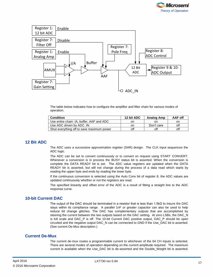
Current De-Mux
The current de-mux routes a programmable current to whichever of the 64 CH inputs is selected.
There are several modes of operation depending on the current amplitude required. The maximum
current is available when the Use_DAC bit is de-asserted and the Double_Weight bit is asserted;
LX7730 rev 0.94 April 2016
© 2016 Microsemi Corporation
18
64 Analog Input RAD Tolerant Telemetry Controller
this provides eight levels ranging from 500uA to 4mA. When both the Use_DAC and
Double_Weight bits are de-asserted there are eight possible levels from 250uA to 2mA. If the
Use_DAC bit is asserted, the 10bit DAC is used to set the de-mux current; each LSB has a weight
of 10uA. A maximum of 300uA is suggested (code 31) when operating in this mode. The current
de-mux can be shut off by asserting the Current Source Disable bit of register 1; the current De-
MUX defaults to the off state at power up and must be enabled.
16 levels0 to 800uA
1024 levels0 to 2mA
DAC_NDAC_P
Register 5: DW & Level
Register 14 & 15:10 bit DAC
Register 6:Current De-Mux
CH1
CH64X 5 Current amp
CurrentDe-MUX
IDAC
Register 5: Use DAC
Register 1
IREFEnable
Fixed Bi-Level Inputs
There are eight fixed bi-level inputs with a 2.5V internal threshold setting common to all detectors.
There is also a register selectable external threshold pin BL_TH where a threshold voltage can be
programmed using a voltage divider to VREF that can be used in place of the internal reference.
These logic threshold detected outputs go directly to output pins so they can be monitored directly
by the FPGA without the delay of the digital interface. A low pass filter and threshold hysteresis
provides high frequency noise rejection.
Power On Reset
In Manual reset mode, the FPGA logically drives the RESET pin directly. The RESET pin should
be asserted and released a few milliseconds after power is applied to place the registers in the
default state. In auto-reset mode, a capacitor should be connected from RESET to GND to provide
SEFI immunity and to program the reset time delay: the time delay from a valid VDD and internal
5V rail within the IC until the reset is released. The equation for this timing is:
RESETCDELAY 35000
FPGA Interface
There are two options provided for the FPGA interface; either a single parallel interface or two SPI
interfaces. Grounding either the SPI_A or SPI_B pin will selected either of these interfaces; these
pins have a 1MΩ pull-up to VDD. Only one interface can be active at any one time, but it is
acceptable to switch between interfaces; this should only be done when the interface is idle or at
rest. The LX7730 executes a command as soon as it has been received with the exception of the
10 bit DAC. The DAC output is updated when the upper byte MSB register is written to.
LX7730 rev 0.94 April 2016
© 2016 Microsemi Corporation 19
Theory of Operation
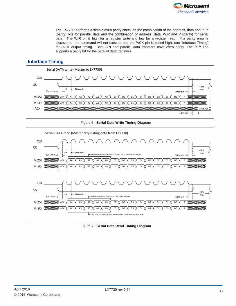
The LX7730 performs a simple even parity check on the combination of the address, data and PTY
(parity) bits for parallel data and the combination of address, data, W/R and P (parity) for serial
data. The W/R bit is high for a register write and low for a register read. If a parity error is
discovered, the command will not execute and the /ACK pin is pulled high, see “Interface Timing”
for /ACK output timing. Both SPI and parallel data transfers have even parity. The PTY line
supports a parity bit for the parallel data transfers.
Interface Timing
SS
MOSI
Serial DATA write (Master to LX7730)
CLK
40nsmin
W/R A4 A3 A2 A1 A0 D7 D6 D5 D4 D3 D2 D1 D0 P
10ns min10ns min
10ns min
MISO W/R A4 A3 A2 A1 A0 D7 D6 D5 D4 D3 D2 D1 D0 P
ACK
10ns min
Valid ACK
10ns min
Figure 6 · Serial Data Write Timing Diagram
SS
MOSI
MISO
Serial DATA read (Master requesting data from LX7730)
CLK
40nsmin
W/R A4 A3 A2 A1 A0 D7 D6 D5 D4 D3 D2 D1 D0 P
W/R A4 A3 A2 A1 A0 D7 D6 D5 D4 D3 D2 D1 D0 P
10ns min10ns min
10ns minAddress of byte to be sent from LX7730 on next data transfer
SS
MOSI
MISO
CLK
40nsmin
W/R A4 A3 A2 A1 A0 D7 D6 D5 D4 D3 D2 D1 D0 P
W/R A4 A3 A2 A1 A0 D7 D6 D5 D4 D3 D2 D1 D0 P
10ns min10ns min
10ns minAddress of byte to be sent on next data transfer
Address and data of byte requested on previous read command
Figure 7 · Serial Data Read Timing Diagram

LX7730 rev 0.94 April 2016
© 2016 Microsemi Corporation
20
64 Analog Input RAD Tolerant Telemetry Controller
ADDRESS
OE
DATA (OUT)
DATA read. (WE remains high.)
ADDRESS
WE
DATA (IN)
DATA write. (OE remains high.)
10ns min
Valid dataValid data
20ns min
20ns min
Valid addrValid addr
10ns max
CE CE
ACK Valid ACK
Figure 8 · Parallel Data Transfer Timing Diagram
Note: For “serial data write” /ACK output is valid after /SS rises. It will remain valid until the next time /SS is pulled low. For
“parallel data write” the /ACK output is valid after the address, data, and PTY signals are stable. The /ACK output should be
low while /CE is low for the data to be written to the registers

LX7730 rev 0.94 April 2016
© 2016 Microsemi Corporation 21
Theory of Operation
Figure 9 · Parallel Data Transfer Timing Diagram for Successive Data Transfers
LX7730 rev 0.94 April 2016
© 2016 Microsemi Corporation
22
64 Analog Input RAD Tolerant Telemetry Controller
Register Descriptions
Register address 0: Master Reset
Register address 0 is used to perform a master reset which returns all internal registers to the
power on (default) state. During the applied reset state, test signals are routed to BLO5 to 8. The
mapping for this is: BLO5 = VCC UVLO, BLO6 = VEE UVLO, BLO7 = +5V UVLO, BLO8 = Power
On Enable. To perform the master reset, the bit code 01101010 must be written to register 0; then,
to restore normal operation a write to register 0 of another code (such as 00000000) is required.
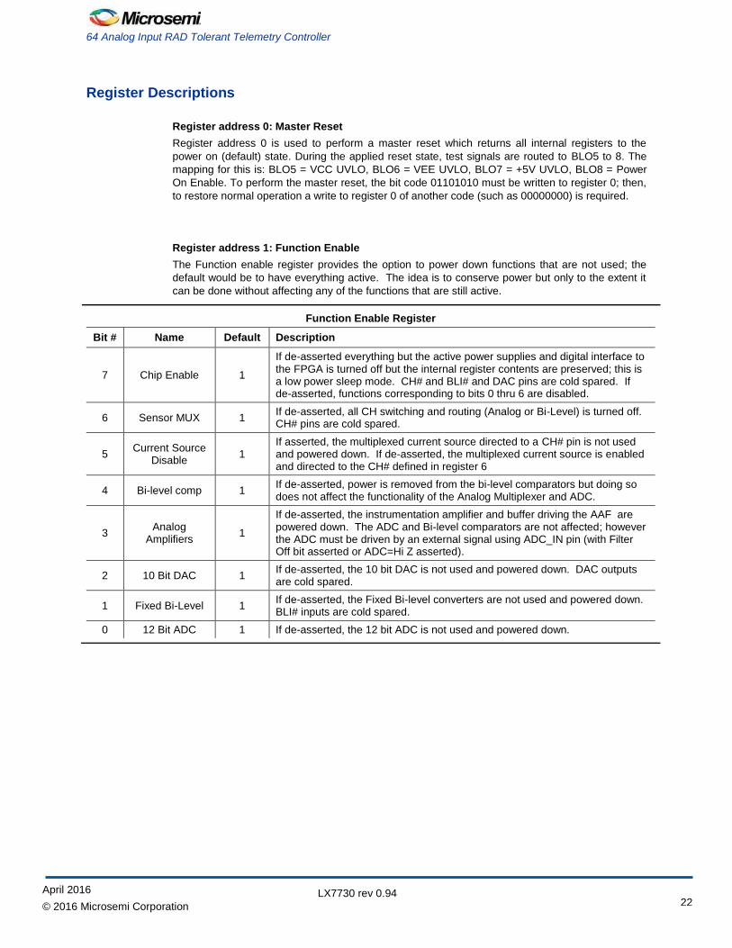
Register address 1: Function Enable
The Function enable register provides the option to power down functions that are not used; the
default would be to have everything active. The idea is to conserve power but only to the extent it
can be done without affecting any of the functions that are still active.
Function Enable Register
Bit # Name Default Description
7 Chip Enable 1
If de-asserted everything but the active power supplies and digital interface to the FPGA is turned off but the internal register contents are preserved; this is a low power sleep mode. CH# and BLI# and DAC pins are cold spared. If de-asserted, functions corresponding to bits 0 thru 6 are disabled.
6 Sensor MUX 1 If de-asserted, all CH switching and routing (Analog or Bi-Level) is turned off. CH# pins are cold spared.
5 Current Source
Disable 1
If asserted, the multiplexed current source directed to a CH# pin is not used and powered down. If de-asserted, the multiplexed current source is enabled and directed to the CH# defined in register 6
4 Bi-level comp 1 If de-asserted, power is removed from the bi-level comparators but doing so does not affect the functionality of the Analog Multiplexer and ADC.
3 Analog
Amplifiers 1
If de-asserted, the instrumentation amplifier and buffer driving the AAF are powered down. The ADC and Bi-level comparators are not affected; however the ADC must be driven by an external signal using ADC_IN pin (with Filter Off bit asserted or ADC=Hi Z asserted).
2 10 Bit DAC 1 If de-asserted, the 10 bit DAC is not used and powered down. DAC outputs are cold spared.
1 Fixed Bi-Level 1 If de-asserted, the Fixed Bi-level converters are not used and powered down. BLI# inputs are cold spared.
0 12 Bit ADC 1 If de-asserted, the 12 bit ADC is not used and powered down.
LX7730 rev 0.94 April 2016
© 2016 Microsemi Corporation 23
Theory of Operation
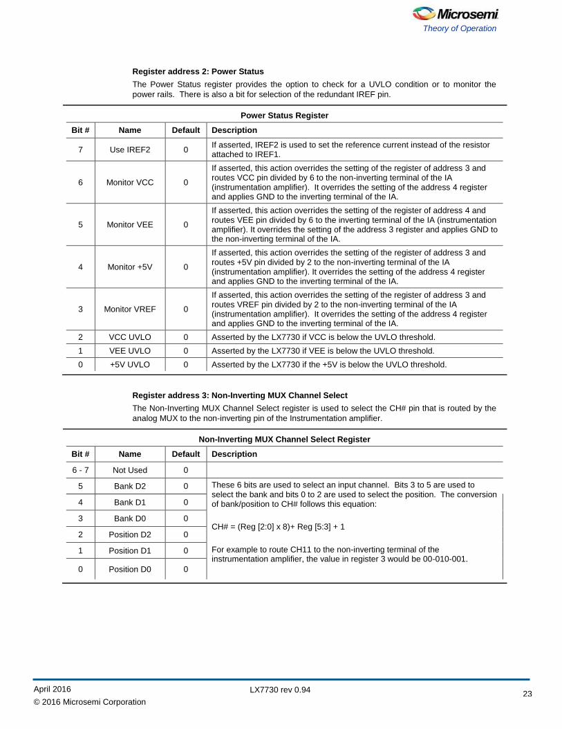
Register address 2: Power Status
The Power Status register provides the option to check for a UVLO condition or to monitor the
power rails. There is also a bit for selection of the redundant IREF pin.
Power Status Register
Bit # Name Default Description
7 Use IREF2 0 If asserted, IREF2 is used to set the reference current instead of the resistor attached to IREF1.
6 Monitor VCC 0
If asserted, this action overrides the setting of the register of address 3 and routes VCC pin divided by 6 to the non-inverting terminal of the IA (instrumentation amplifier). It overrides the setting of the address 4 register and applies GND to the inverting terminal of the IA.
5 Monitor VEE 0
If asserted, this action overrides the setting of the register of address 4 and routes VEE pin divided by 6 to the inverting terminal of the IA (instrumentation amplifier). It overrides the setting of the address 3 register and applies GND to the non-inverting terminal of the IA.
4 Monitor +5V 0
If asserted, this action overrides the setting of the register of address 3 and routes +5V pin divided by 2 to the non-inverting terminal of the IA (instrumentation amplifier). It overrides the setting of the address 4 register and applies GND to the inverting terminal of the IA.
3 Monitor VREF 0
If asserted, this action overrides the setting of the register of address 3 and routes VREF pin divided by 2 to the non-inverting terminal of the IA (instrumentation amplifier). It overrides the setting of the address 4 register and applies GND to the inverting terminal of the IA.
2 VCC UVLO 0 Asserted by the LX7730 if VCC is below the UVLO threshold.
1 VEE UVLO 0 Asserted by the LX7730 if VEE is below the UVLO threshold.
0 +5V UVLO 0 Asserted by the LX7730 if the +5V is below the UVLO threshold.
Register address 3: Non-Inverting MUX Channel Select
The Non-Inverting MUX Channel Select register is used to select the CH# pin that is routed by the
analog MUX to the non-inverting pin of the Instrumentation amplifier.
Non-Inverting MUX Channel Select Register
Bit # Name Default Description
6 - 7 Not Used 0
5 Bank D2 0 These 6 bits are used to select an input channel. Bits 3 to 5 are used to select the bank and bits 0 to 2 are used to select the position. The conversion of bank/position to CH# follows this equation:
CH# = (Reg [2:0] x 8)+ Reg [5:3] + 1
For example to route CH11 to the non-inverting terminal of the instrumentation amplifier, the value in register 3 would be 00-010-001.
4 Bank D1 0
3 Bank D0 0
2 Position D2 0
1 Position D1 0
0 Position D0 0
LX7730 rev 0.94 April 2016
© 2016 Microsemi Corporation
24
64 Analog Input RAD Tolerant Telemetry Controller
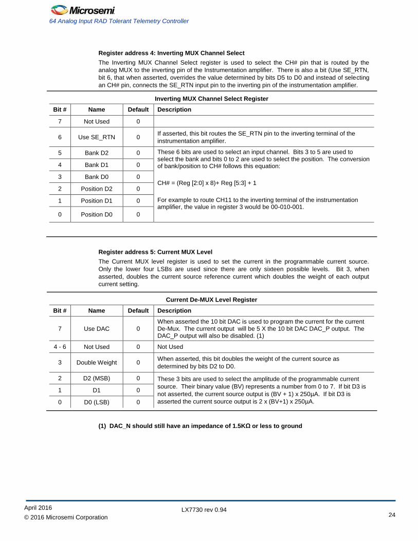
Register address 4: Inverting MUX Channel Select
The Inverting MUX Channel Select register is used to select the CH# pin that is routed by the
analog MUX to the inverting pin of the Instrumentation amplifier. There is also a bit (Use SE_RTN,
bit 6, that when asserted, overrides the value determined by bits D5 to D0 and instead of selecting
an CH# pin, connects the SE_RTN input pin to the inverting pin of the instrumentation amplifier.
Inverting MUX Channel Select Register
Bit # Name Default Description
7 Not Used 0
6 Use SE_RTN 0 If asserted, this bit routes the SE_RTN pin to the inverting terminal of the
instrumentation amplifier.
5 Bank D2 0 These 6 bits are used to select an input channel. Bits 3 to 5 are used to select the bank and bits 0 to 2 are used to select the position. The conversion of bank/position to CH# follows this equation:
CH# = (Reg [2:0] x 8)+ Reg [5:3] + 1
For example to route CH11 to the inverting terminal of the instrumentation amplifier, the value in register 3 would be 00-010-001.
4 Bank D1 0
3 Bank D0 0
2 Position D2 0
1 Position D1 0
0 Position D0 0
Register address 5: Current MUX Level
The Current MUX level register is used to set the current in the programmable current source.
Only the lower four LSBs are used since there are only sixteen possible levels. Bit 3, when
asserted, doubles the current source reference current which doubles the weight of each output
current setting.
Current De-MUX Level Register
Bit # Name Default Description
7 Use DAC 0 When asserted the 10 bit DAC is used to program the current for the current De-Mux. The current output will be 5 X the 10 bit DAC DAC_P output. The DAC_P output will also be disabled. (1)
4 - 6 Not Used 0 Not Used
3 Double Weight 0 When asserted, this bit doubles the weight of the current source as
determined by bits D2 to D0.
2 D2 (MSB) 0 These 3 bits are used to select the amplitude of the programmable current
source. Their binary value (BV) represents a number from 0 to 7. If bit D3 is
not asserted, the current source output is (BV + 1) x 250µA. If bit D3 is
asserted the current source output is 2 x (BV+1) x 250µA.
1 D1 0
0 D0 (LSB) 0
(1) DAC_N should still have an impedance of 1.5KΩ or less to ground
LX7730 rev 0.94 April 2016
© 2016 Microsemi Corporation 25
Theory of Operation
Register address 6: Current MUX Channel Selection
The Current MUX Select register is used to route the current source to one of the 64 input channels
(CH#).
Current MUX Channel Selection Register
Bit # Name Default Description
6 - 7 Not Used 0 Not Used
5 D5 (MSB) 0
These 6 bits are used to select an input channel. Their binary value
represents a number from 0 to 63. The CH# pin selected is their binary value
plus 1. For example value D5 to D0 = 011011, or binary 27 will route the
output of the programmable current source to CH28.
4 D4 0
3 D3 0
2 D2 0
1 D1 0
0 D0 (LSB) 0
Register address 7: Signal Conditioning Amplifier
The Signal Conditioning Amplifier register controls the gain and pole location for the signal
conditioning amplifier located between the output of the instrumentation amplifier and the input to
the ADC. It can be shut off to facilitate bypassing or using external signal.
Signal Conditioning Amplifier Register
Bit # Name Default Description
7 Not Used 0 Not Used
6 AAF off 0
If de-asserted (and ADC=HiZ is also de-asserted) , the AAF amplifier is fully
functional and the output of the AAF drives the ADC input with a low
impedance driver. When asserted, the AAF filter is off and the ADC can be
driven from ADC_IN.
5 Second Pole
Frequency MSB 0 These two pins are used to select the pole frequency for a single pole
response for one of two possible single pole filters. The frequency settings
are [D5, D4] = 00, 01, 10 for 400, 2k, 10k in Hertz, respectively (setting 11 is
not used). 4 Second Pole
Frequency LSB 0
3 First Pole
Frequency MSB 0 These two pins are used to select the pole frequency for a single pole
response for one of two possible single pole filters. The frequency settings
are [D3, D2] = 00, 01, 10for 400, 2k, 10k in Hertz, respectively (setting 11 is
not used). 2 First Pole
Frequency LSB 0
1 Gain Setting
MSB 0 These two pins are used to select the gain setting for the amplifier channel.
The gain settings are [D1,D0] = 00, 01, 10 for a gain of 0.4, 2.0, or 10. The
[D1,D0] = 11 setting is not used (but also sets a gain of 10). 0 Gain Setting
LSB 0
LX7730 rev 0.94 April 2016
© 2016 Microsemi Corporation
26
64 Analog Input RAD Tolerant Telemetry Controller
Register address 8: Analog to Digital Converter Control
The ADC Converter Control register allows the FPGA to initiate a sampling or continuous sampling.
It also indicates the status of the ADC.
Analog to Digital Converter Control Register
Bit # Name Default Description
7
Auto Sample
Rate
0 This register is used to slow down the auto sample rate of the ADC. The auto
sample rate is set to multiples of the Sample Period (tSAMP).The register bits 7,
6, 5 represent a binary value “N” with bit 7 representing the MSB. This 3 bit
binary value sets the ADC auto sample rate = tSAMP x 2N.
6 0
5 0
4 Auto Conv 0 If asserted, the ADC performs continuous conversions. ADC conversions are
stored until the next value is ready and then overwritten.
3 Data Ready 0
This bit is asserted by the LX7730 when the ADC finishes a conversion and
stays asserted until Start Conv is asserted or the Auto Conv timer begins
another conversion.
2 Busy 0 This bit is asserted by the LX7730 while the ADC is performing a conversion.
1 Start Conv 0 If asserted, this bit starts a single conversion process of the ADC.
0 ADC_IN = HI_Z 0
If de-asserted (and AAF off is also de-asserted) , the AAF amplifier is fully
functional and the output of the AAF drives the ADC input with a low
impedance driver. When asserted, the AAF filter is off and the ADC can be
driven from ADC_IN.
Register address 9: ADC Upper Byte
The ADC Upper Byte register contains the most significant eight bits from the last completed ADC
conversion.
ADC Upper Byte
Bit # Name Default Description
7 D11 (MSB) 0
Eight most significant bits from last completed ADC conversion. The combined ADC output from registers 9 and 10 represents a value that is 12 bits long.
From the ADC input, the ADC value represents: ([12 bit value]/4095) x 2.0
6 D10 0
5 D9 0
4 D8 0
3 D7 0
2 D6 0
1 D5 0
0 D4 0
LX7730 rev 0.94 April 2016
© 2016 Microsemi Corporation 27
Theory of Operation
Register address 10: ADC Lower Bits
The ADC Lower Bits register contains the least significant four bits from the last completed ADC
conversion.
ADC Lower Bits
Bit # Name Default Description
4 - 7 Not Used 0 Not Used
3 D3 0 Four least significant bits from last completed ADC conversion. The combined ADC output from registers 9 and 10 represents a value that is 12 bits long. From the ADC input, the ADC value represents:
([12 bit value]/4095) x 2.0
2 D2 0
1 D1 0
0 D0 (LSB) 0
Register address 11: Bi Level Threshold DAC
The Bi Level Threshold DAC register contains the digital value that controls the 8 bit Digital to
Analog converter output.
Bi Level Threshold DAC Register
Bit # Name Default Description
7 D7 (MSB) 0
Eight bits for setting the Bi-Level Threshold. The Bi-Level Threshold level is:
([Reg 11 value]/255) x 5V
6 D6 0
5 D5 0
4 D4 0
3 D3 0
2 D2 0
1 D1 0
0 D0 (LSB) 0
Register address 12: Bi-Level Bank Switch Position and Fixed Bi-Level Optional Input
The Bi-Level Bank Switch Position register selects one of the eight switch positions form the eight
banks of inputs to be routed to the eight Bi-Level comparators. The fixed Bi-Level inputs (not
related to the Bi-Level Banks) has an optional external threshold setting input which can be
selected using the MSB of this register.
Bi-Level Bank Switch Position and Fixed Bi-Level Optional Input Register
Bit # Name Default Description
7 Use BL-TH 0 Asserting this bit selects the external BL_TH pin for the Fixed Bi-Level inputs.
4 - 6 Not Used 0 Not Used
3 En BL Sw Pos 0 Asserting this bit enable the selection of the Bi-Level Bank Switch Position.
2 D2 (MSB) 0 These 3 bits are used to select a common switch position for the eight bi-level multiplexers. The binary value represents a number from 0 to 7. The switch position selected is their binary value plus 1. For example value [D2, D1, D0] = 011, or binary 3 will select switch position 4 or route CH25 to CH32 to the bi-level comparators.
1 D1 0
0 D0 (LSB) 0

LX7730 rev 0.94 April 2016
© 2016 Microsemi Corporation
28
64 Analog Input RAD Tolerant Telemetry Controller
Register address 13: Bi-Level Status
The Bi-Level status register has a bit dedicated to each threshold comparator output. The bit is
asserted if the selected CH# channel voltage is greater than the reference as determined by the Bi-
Level Threshold DAC register.
Bi-Level Status Register
Bit # Name Default Description
7 Comparator 8 0 Comparator for channels: ([REG 12]+1) x 8
6 Comparator 7 0 Comparator for channels: ([REG 12]+1) x 8 - 1
5 Comparator 6 0 Comparator for channels: ([REG 12]+1) x 8 - 2
4 Comparator 5 0 Comparator for channels: ([REG 12]+1) x 8 - 3
3 Comparator 4 0 Comparator for channels: ([REG 12]+1) x 8 - 4
2 Comparator 3 0 Comparator for channels: ([REG 12]+1) x 8 - 5
1 Comparator 2 0 Comparator for channels: ([REG 12]+1) x 8 - 6
0 Comparator 1 0 Comparator for channels: ([REG 12]+1) x 8 - 7
Register address 14: 10 Bit DAC Upper Byte
The 10 Bit DAC Upper Byte register contains the upper eight most significant bits for the digital
value that controls the outputs of the 10 Bit Current Digital to Analog converter.
10 Bit DAC Upper Byte
Bit # Name Default Description
7 D7 (MSB) 0
Eight most significant bits for setting the outputs of the 10 Bit Current DAC. Combined with the two least significant bits from register 15, this makes up a 10 bit value The Current DAC output currents are (with Riref = 20k):
DAC_P = ([10 Bit value]/1023) x 2mA
DAC_N = [1 - ([10 Bit value]/1023) x 2mA
When the upper byte is written, both the upper byte and lower byte are changed to the values stored in registers 14 and 15.
6 D6 0
5 D5 0
4 D4 0
3 D3 0
2 D2 0
1 D1 0
0 D0 (LSB) 0
Register address 15: 10 Bit DAC Lower Bits
The 10 Bit DAC Lower Byte register contains the two least significant bits for the digital value that
controls the outputs of the 10 Bit Current Digital to Analog.
10 Bit DAC Lower Bits Register
Bit # Name Default Description
2 - 7 Not used 0 Not Used
1 D1 0 Two least significant bits for setting the outputs of the 10 Bit Current DAC. Combined with the eight most significant bits from register 14, this makes up a 10 bit value The Current DAC output currents are (with Riref = 20k):
DAC_P = ([10 Bit value]/1023) x 2mA
DAC_N = [1 - ([10 Bit value]/1023) x 2mA
The lower byte is not loaded until the upper byte register is written.
0 D0 (LSB) 0

LX7730 rev 0.94 April 2016
© 2016 Microsemi Corporation 29
Theory of Operation
Register address 16: Calibration
The Calibration register is used to perform calibration of the amplifier offset and FPGA assisted
testing of the multiplexer switches and programmable current source multiplexer.
Calibration Register
Bit # Name Default Description
7 IA Short 0 If asserted, this action overrides the setting of the register of address 4 and causes a switch closure which shorts the inverting terminal of the instrumentation amplifier to the non-inverting terminal.
6 Not used 0
5 Not used 0
4 Cont Check 0 If asserted, a current source is applied to the non-inverting input of the instrumentation amplifier.
3 NP Cont Check 0 If asserted, a current source is applied to the inverting input of the instrumentation amplifier and the non-inverting terminal is connected to VREF.
2 Not used 0
1 I GND 0 If asserted, this action overrides the setting of the register of address 4 and causes a switch closure which shorts the inverting terminal of the instrumentation amplifier to IC GND.
0 Not Used 0
Register address 17: OTP
The OTP register enables the user to read the default OTP bits and adjusts the bits as required.
Power and Reference Adjust Register
Bit # Name Default Description
2 - 7 Not Used 0 Not Used
1 OTP out select 0 If this bit is asserted the OTP outputs will be set by registers 18 through 22. If
this bit is not asserted the OTP will out be set by internal programming bits
0 OTP in select 0 If this bit is asserted the default OTP bits are read into register 18 through 22.
Built-In Test and Adjustment Features
The following test features allow for checking and adjusting the LX7730.
Amplifier Offset calibration: There are two features that can be used to calibrate the offset
voltage of the sample amplifier chain. The first feature is a “shorting switch” that can be closed
across the input to the instrumentation amplifier. This switch is activated by asserting the IA
SHORT register. (See figure #9)
LX7730 rev 0.94 April 2016
© 2016 Microsemi Corporation
30
64 Analog Input RAD Tolerant Telemetry Controller
P_PolarityRegister
4
SELBANK1BANK2BANK3BANK4BANK5BANK6BANK7BANK8ITEST
GND
VCC_DIVNU+5V_DIVVREF_DIVNUNU
SELBANK1BANK2BANK3BANK4BANK5BANK6BANK7BANK8SE_RTN
NU
IA_SHORTGNDVEE_DIVNUNUNUIncrement
4
Up/DownCounter
+-
N_PolarityRegister
4
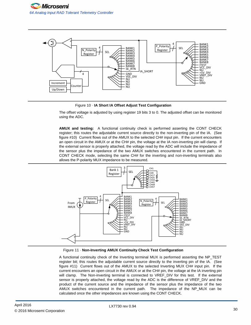
Figure 10 · IA Short IA Offset Adjust Test Configuration
The offset voltage is adjusted by using register 19 bits 3 to 0. The adjusted offset can be monitored
using the ADC.
AMUX and testing: A functional continuity check is performed asserting the CONT CHECK
register; this routes the adjustable current source directly to the non-inverting pin of the IA. (See
figure #10) Current flows out of the AMUX to the selected CH# input pin. If the current encounters
an open circuit in the AMUX or at the CH# pin, the voltage at the IA non-inverting pin will clamp. If
the external sensor is properly attached, the voltage read by the ADC will include the impedance of
the sensor plus the impedance of the two AMUX switches encountered in the current path. In
CONT CHECK mode, selecting the same CH# for the inverting and non-inverting terminals also
allows the P-polarity MUX impedance to be measured.
P_PolarityRegister
4
SEL BANK2BANK3BANK4BANK5BANK6BANK7BANK8ITEST
SELBANK1BANK2BANK3BANK4BANK5BANK6BANK7BANK8SE_RTN
NU
IA_SHORTGNDVEE_DIVNUNUNU
+-
N_PolarityRegister
4BANK1
From IMUX
Bank 1Register
3
SELCH1
CH9CH17CH25CH33CH41CH49CH57
GND
VCC_DIVNU+5V_DIVVREF_DIVNUNU
Figure 11 · Non-Inverting AMUX Continuity Check Test Configuration
A functional continuity check of the Inverting terminal MUX is performed asserting the NP_TEST
register bit; this routes the adjustable current source directly to the inverting pin of the IA. (See
figure #11) Current flows out of the AMUX to the selected Inverting MUX CH# input pin. If the
current encounters an open circuit in the AMUX or at the CH# pin, the voltage at the IA inverting pin
will clamp. The Non-inverting terminal is connected to VREF_DIV for this test. If the external
sensor is properly attached, the voltage read by the ADC is the difference of VREF_DIV and the
product of the current source and the impedance of the sensor plus the impedance of the two
AMUX switches encountered in the current path. The impedance of the NP_MUX can be
calculated once the other impedances are known using the CONT CHECK.
LX7730 rev 0.94 April 2016
© 2016 Microsemi Corporation 31
Theory of Operation
P_PolarityRegister
4
SEL BANK2BANK3BANK4BANK5BANK6BANK7BANK8ITEST
SELBANK1BANK2BANK3BANK4BANK5BANK6BANK7BANK8SE_RTN
NU
IA_SHORTGNDVEE_DIVNUNUNU
+-
N_PolarityRegister
4BANK1
From IMUX
Bank 1Register
3
SELCH1
CH9CH17CH25CH33CH41CH49CH57
GND
VCC_DIVNU+5V_DIVVREF_DIVNUNU
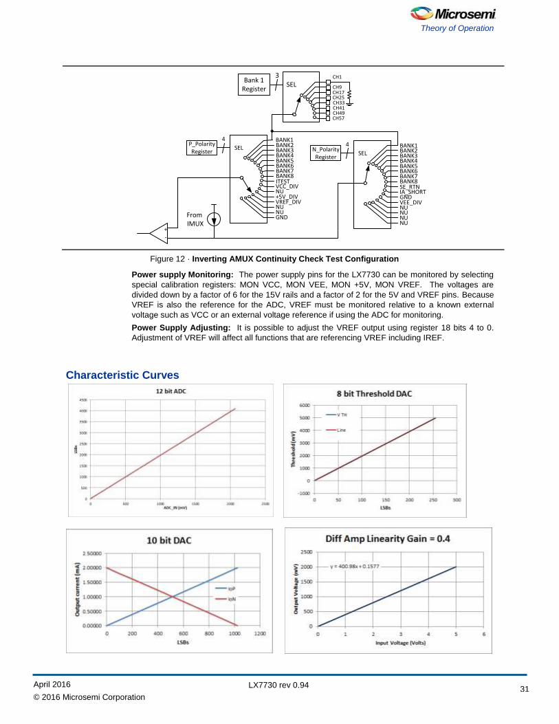
Figure 12 · Inverting AMUX Continuity Check Test Configuration
Power supply Monitoring: The power supply pins for the LX7730 can be monitored by selecting
special calibration registers: MON VCC, MON VEE, MON +5V, MON VREF. The voltages are
divided down by a factor of 6 for the 15V rails and a factor of 2 for the 5V and VREF pins. Because
VREF is also the reference for the ADC, VREF must be monitored relative to a known external
voltage such as VCC or an external voltage reference if using the ADC for monitoring.
Power Supply Adjusting: It is possible to adjust the VREF output using register 18 bits 4 to 0.
Adjustment of VREF will affect all functions that are referencing VREF including IREF.
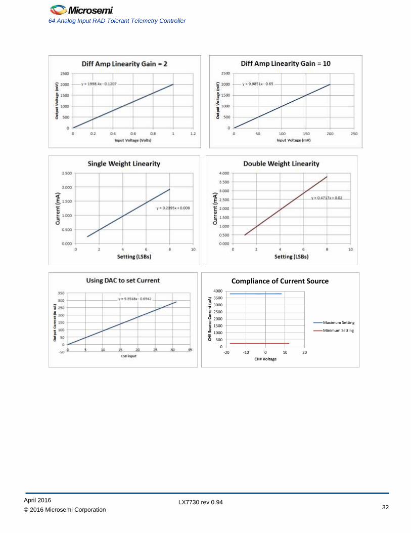
Characteristic Curves
LX7730 rev 0.94 April 2016
© 2016 Microsemi Corporation
32
64 Analog Input RAD Tolerant Telemetry Controller
0
500
1000
1500
2000
2500
3000
3500
4000
-20 -10 0 10 20
CH
# So
urc
e C
urr
en
t (u
A)
CH# Voltage
Compliance of Current Source
Maximum Setting
Minimum Setting
LX7730 rev 0.94 April 2016
© 2016 Microsemi Corporation 33
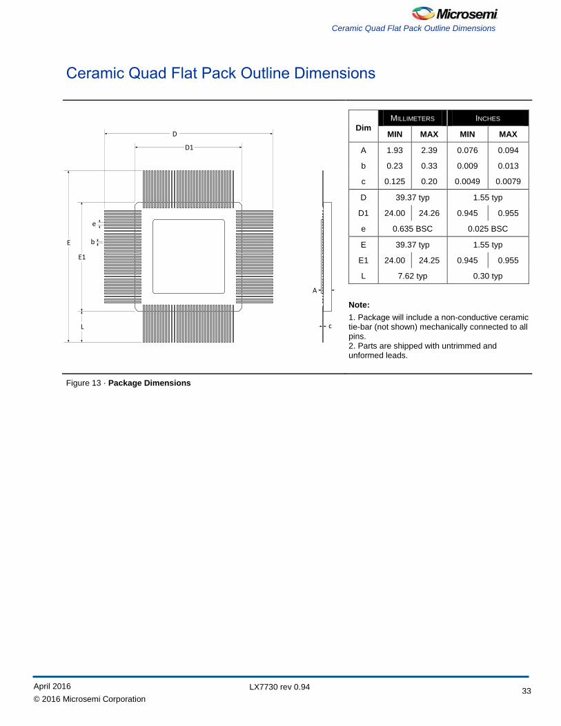
Ceramic Quad Flat Pack Outline Dimensions
Ceramic Quad Flat Pack Outline Dimensions
b
e
E1
E
D1
D
L c
A
Note:
1. 1. Package will include a non-conductive ceramic tie-bar (not shown) mechanically connected to all pins.
2. 2. Parts are shipped with untrimmed and unformed leads.
Dim
MILLIMETERS INCHES
MIN MAX MIN MAX
A 1.93 2.39 0.076 0.094
b 0.23 0.33 0.009 0.013
c 0.125 0.20 0.0049 0.0079
D 39.37 typ 1.55 typ
D1 24.00 24.26 0.945 0.955
e 0.635 BSC 0.025 BSC
E 39.37 typ 1.55 typ
E1 24.00 24.25 0.945 0.955
L 7.62 typ 0.30 typ
Figure 13 · Package Dimensions
LX7730 0.94/02.16
Microsemi Corporation (Nasdaq: MSCC) offers a comprehensive portfolio of semiconductor
and system solutions for communications, defense & security, aerospace and industrial
markets. Products include high-performance and radiation-hardened analog mixed-signal
integrated circuits, FPGAs, SoCs and ASICs; power management products; timing and
synchronization devices and precise time solutions, setting the world’s standard for time; voice
processing devices; RF solutions; discrete components; security technologies and scalable
anti-tamper products; Power-over-Ethernet ICs and midspans; as well as custom design
capabilities and services. Microsemi is headquartered in Aliso Viejo, Calif., and has
approximately 3,400 employees globally. Learn more at www.microsemi.com.
Microsemi makes no warranty, representation, or guarantee regarding the information contained herein or
the suitability of its products and services for any particular purpose, nor does Microsemi assume any
liability whatsoever arising out of the application or use of any product or circuit. The products sold
hereunder and any other products sold by Microsemi have been subject to limited testing and should not
be used in conjunction with mission-critical equipment or applications. Any performance specifications are
believed to be reliable but are not verified, and Buyer must conduct and complete all performance and
other testing of the products, alone and together with, or installed in, any end-products. Buyer shall not
rely on any data and performance specifications or parameters provided by Microsemi. It is the Buyer’s
responsibility to independently determine suitability of any products and to test and verify the same. The
information provided by Microsemi hereunder is provided “as is, where is” and with all faults, and the
entire risk associated with such information is entirely with the Buyer. Microsemi does not grant, explicitly
or implicitly, to any party any patent rights, licenses, or any other IP rights, whether with regard to such
information itself or anything described by such information. Information provided in this document is
proprietary to Microsemi, and Microsemi reserves the right to make any changes to the information in this
document or to any products and services at any time without notice.
Microsemi Corporate Headquarters One Enterprise, Aliso Viejo, CA 92656 USA Within the USA: +1 (800) 713-4113 Outside the USA: +1 (949) 380-6100 Sales: +1 (949) 380-6136 Fax: +1 (949) 215-4996
E-mail: [email protected]
© 2016 Microsemi Corporation. All rights reserved. Microsemi and the Microsemi logo are trademarks of Microsemi Corporation. All other trademarks and service marks are the property of their respective owners.