Embed Size (px)
Citation preview
APPENDIX B
SPICE DEVICE MODELS AND SIMULATIONEXAMPLES
Introduction
This appendix is concerned with the very important topic of using SPICE to simulatethe operation of electronic circuits. We described the need for and the role of computersimulation in circuit design in the preface. This Appendix presents a brief description ofthe models that SPICE uses to describe the operation of op amps, diodes, MOSFETs, andBJTs. Furthermore, this Appendix is accompanied by design and simulation examples usingSPICE simulators, including instructions on how to install and use the simulators, SPICEnetlists for the examples, and a summary of the simulation results that can be expected. Allof these resources are available via the book website.
Contents
B.1 SPICE Device Models B-2B.1.1 The Op-Amp Model B-2B.1.2 The Diode Model B-4B.1.3 The Zener Diode Model B-6B.1.4 MOSFET Models B-6B.1.5 The BJT Model B-10
B.2 SPICE Examples B-13S.2.1 Performance of a Noninverting Amplifier B-13S.2.2 Characteristics of the 741 Op Amp B-16S.4.1 Design of a DC Power Supply B-19S.6.1 Dependence of the BJT. β on the Bias Circuit B-24S.7.1 The CS Amplifier B-25S.7.2 The CE Amplifier with Emitter Resistance B-28S.7.3 Design of a CMOS CS Amplifier B-31S.8.1 The CS Amplifier with Active Load B-36S.9.1 A Multistage Differential BJT Amplifier B-39S.9.2 The Two-Stage CMOS Op Amp B-46S.10.1 Frequency Response of the CMOS CS and the Folded-Cascode
Amplifiers B-52S.10.2 Frequency Response of the Discrete CS Amplifier B-58S.11.1 Determining the Loop Gain of a Feedback Amplifier B-61S.11.2 A Two-Stage CMOS Op Amp with Series-Shunt Feedback B-65S.12.1 Class B BJT Output Stage B-71S.13.1 Frequency Compensation of the Two-Stage CMOS Op Amp B-75
B-1©20 Oxford University PressReprinting or distribution, electronically or otherwise, without the express written consent of Oxford University Press is prohibited.
20
B-2 Appendix B SPICE Device Models and Simulation Examples
S.14.1 Verification of the Design of a Fifth-Order Chebyshev Filter B-80S.14.2 Effect of Finite Op-Amp Bandwidth on the Operation of the
Two-Integrator-Loop Filter B-82S.15.1 Wien-Bridge Oscillator B-86S.15.2 Active-Filter-Tuned Oscillator B-88S.16.1 Operation of the CMOS Inverter B-90
B.1 SPICE Device Models
To the designer, the value of simulation results depends entirely on the quality of the modelsused for the devices. The more faithfully the models represent the devices’ characteristics,the more accurately the simulation results will describe the operation of an actual circuit.Device nonidealities must be included in the device model, otherwise their impact will notappear in the simulation results.
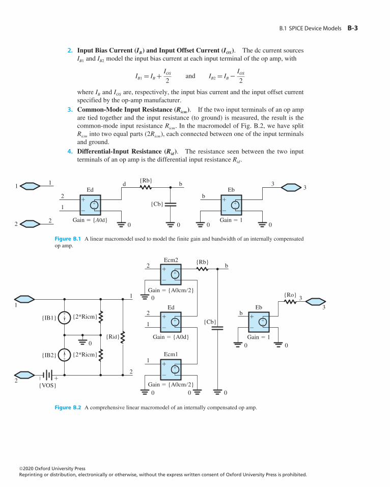
B.1.1 The Op-Amp Model
In simulating circuits that use one or more op amps, amacromodel can be used to representeach op amp. A macromodel is based on the observed terminal characteristics of the op amprather than on the modeling of every transistor in the op-amp internal circuit. Macromodelscan be developed from data-sheet specifications without knowing the details of the internalcircuitry of the op amp.
Linear Macromodel A linear macromodel for an internally compensated op amp withfinite gain and bandwidth is shown in Fig. B.1. In this equivalent-circuit model, the gainconstant A0d of the voltage-controlled voltage source Ed corresponds to the differential gainof the op amp at dc. Resistor Rb and capacitor Cb form a single-time-constant (STC) filterwith a corner frequency
fb = 1
2πRbCb
(B.1)
The low-pass response of this filter is used to model the frequency response of the internallycompensated op amp. The values of Rb and Cb used in the macromodel are chosen such thatfb corresponds to the 3-dB frequency of the op amp being modeled. This is done by arbitrarilyselecting a value for either Rb or Cb (the selected value does not need to be a practical one)and then using Eq. (B.1) to compute the other value. In Fig. B.1, the voltage-controlledvoltage source Eb with a gain constant of unity is used as a buffer to isolate the low-pass filterfrom any load at the op-amp output. Thus any op-amp loading will not affect the frequencyresponse of the filter and hence that of the op amp.
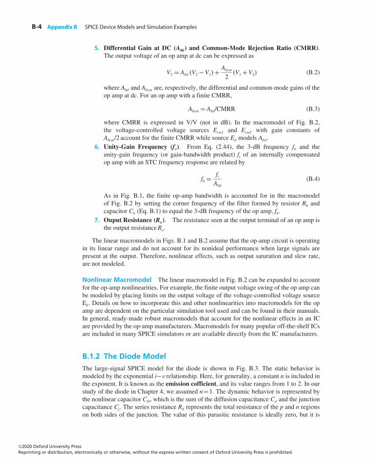
The linear macromodel in Fig. B.1 can be further expanded to account for other op-ampnonidealities. For example, the equivalent-circuit model in Fig. B.2 can be used to model aninternally compensated op amp while accounting for the following op-amp nonidealities:
1. Input Offset Voltage (VOS). The dc voltage source VOS models the op-amp inputoffset voltage.
©20 Oxford University PressReprinting or distribution, electronically or otherwise, without the express written consent of Oxford University Press is prohibited.
20
B.1 SPICE Device Models B-3
2. Input Bias Current (IB) and Input Offset Current (IOS). The dc current sourcesIB1 and IB2 model the input bias current at each input terminal of the op amp, with
IB1 = IB + IOS2
and IB2 = IB − IOS2
where IB and IOS are, respectively, the input bias current and the input offset currentspecified by the op-amp manufacturer.
3. Common-Mode Input Resistance (Ricm). If the two input terminals of an op ampare tied together and the input resistance (to ground) is measured, the result is thecommon-mode input resistance Ricm. In the macromodel of Fig. B.2, we have splitRicm into two equal parts (2Ricm), each connected between one of the input terminalsand ground.
4. Differential-Input Resistance (Rid). The resistance seen between the two inputterminals of an op amp is the differential input resistance Rid.
{Cb}
{Rb}
2
11
1
Gain � {A0d}
Edbd
0 022
�
�
��
b
33
Gain � 1
Eb
0 0
�
�
��
Figure B.1 A linear macromodel used to model the finite gain and bandwidth of an internally compensatedop amp.
{IB1}
{IB2}
{VOS}
{2*Ricm}
{2*Ricm}
1
1
0
2
2
{Rid}
��
Ecm1
Ed
Ecm2
{Cb}
{Rb}2 b
1
Gain � {A0cm�2}
Gain � {A0cm�2}
0
0 0 0
2
1
Gain � {A0d}
�
�
��
�
�
��
�
�
��
�
�
�
�
{Ro}
0
b
3
3
Gain � 10
Eb
�
�
��
Figure B.2 A comprehensive linear macromodel of an internally compensated op amp.
©20 Oxford University PressReprinting or distribution, electronically or otherwise, without the express written consent of Oxford University Press is prohibited.
20
B-4 Appendix B SPICE Device Models and Simulation Examples
5. Differential Gain at DC (A0d) and Common-Mode Rejection Ratio (CMRR).The output voltage of an op amp at dc can be expressed as
V3 = A0d (V2 −V1)+ A0cm
2(V1 +V2) (B.2)
where A0d and A0cm are, respectively, the differential and common-mode gains of theop amp at dc. For an op amp with a finite CMRR,
A0cm = A0d/CMRR (B.3)
where CMRR is expressed in V/V (not in dB). In the macromodel of Fig. B.2,the voltage-controlled voltage sources Ecm1 and Ecm2 with gain constants ofA0cm/2 account for the finite CMRR while source Ed models A0d.
6. Unity-Gain Frequency (f t). From Eq. (2.44), the 3-dB frequency fb and theunity-gain frequency (or gain-bandwidth product) ft of an internally compensatedop amp with an STC frequency response are related by
fb = ftA0d
(B.4)
As in Fig. B.1, the finite op-amp bandwidth is accounted for in the macromodelof Fig. B.2 by setting the corner frequency of the filter formed by resistor Rb andcapacitor Cb (Eq. B.1) to equal the 3-dB frequency of the op amp, fb.
7. Ouput Resistance (Ro). The resistance seen at the output terminal of an op amp isthe output resistanceRo.
The linear macromodels in Figs. B.1 and B.2 assume that the op-amp circuit is operatingin its linear range and do not account for its nonideal performance when large signals arepresent at the output. Therefore, nonlinear effects, such as output saturation and slew rate,are not modeled.
Nonlinear Macromodel The linear macromodel in Fig. B.2 can be expanded to accountfor the op-amp nonlinearities. For example, the finite output voltage swing of the op amp canbe modeled by placing limits on the output voltage of the voltage-controlled voltage sourceEb. Details on how to incorporate this and other nonlinearities into macromodels for the opamp are dependent on the particular simulation tool used and can be found in their manuals.In general, ready-made robust macromodels that account for the nonlinear effects in an ICare provided by the op-amp manufacturers. Macromodels for many popular off-the-shelf ICsare included in many SPICE simulators or are available directly from the IC manufacturers.
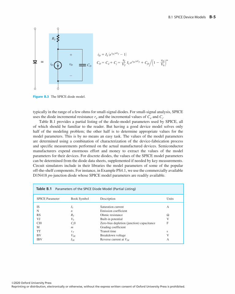
B.1.2 The Diode Model
The large-signal SPICE model for the diode is shown in Fig. B.3. The static behavior ismodeled by the exponential i−v relationship. Here, for generality, a constant n is included inthe exponent. It is known as the emission cofficient, and its value ranges from 1 to 2. In ourstudy of the diode in Chapter 4, we assumed n=1. The dynamic behavior is represented bythe nonlinear capacitor CD, which is the sum of the diffusion capacitance Cd and the junctioncapacitance Cj. The series resistance RS represents the total resistance of the p and n regionson both sides of the junction. The value of this parasitic resistance is ideally zero, but it is
©20 Oxford University PressReprinting or distribution, electronically or otherwise, without the express written consent of Oxford University Press is prohibited.
20
B.1 SPICE Device Models B-5
Figure B.3 The SPICE diode model.
typically in the range of a few ohms for small-signal diodes. For small-signal analysis, SPICEuses the diode incremental resistance rd and the incremental values of Cd and Cj.
Table B.1 provides a partial listing of the diode-model parameters used by SPICE, allof which should be familiar to the reader. But having a good device model solves onlyhalf of the modeling problem; the other half is to determine appropriate values for themodel parameters. This is by no means an easy task. The values of the model parametersare determined using a combination of characterization of the device-fabrication processand specific measurements performed on the actual manufactured devices. Semiconductormanufacturers expend enormous effort and money to extract the values of the modelparameters for their devices. For discrete diodes, the values of the SPICE model parameterscan be determined from the diode data sheets, supplemented if needed by key measurements.Circuit simulators include in their libraries the model parameters of some of the popularoff-the-shelf components. For instance, in Example PS4.1, we use the commercially availableD1N418 pn-junction diode whose SPICE model parameters are readily available.
Table B.1 Parameters of the SPICE Diode Model (Partial Listing)
SPICE Parameter Book Symbol Description Units
IS IS Saturation current AN n Emission coefficientRS RS Ohmic resistance �
VJ V0 Built-in potential VCJ0 Cj0 Zero-bias depletion (junction) capacitance FM m Grading coefficientTT τ T Transit time sBV VZK Breakdown voltage VIBV IZK Reverse current at VZK A
©20 Oxford University PressReprinting or distribution, electronically or otherwise, without the express written consent of Oxford University Press is prohibited.
20
B-6 Appendix B SPICE Device Models and Simulation Examples
D2
D1
rz
VZ0
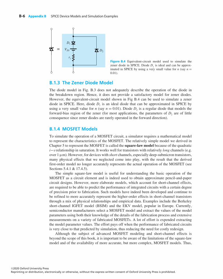
Figure B.4 Equivalent-circuit model used to simulate thezener diode in SPICE. Diode D1 is ideal and can be approx-imated in SPICE by using a very small value for n (say n =0.01).
B.1.3 The Zener Diode Model
The diode model in Fig. B.3 does not adequately describe the operation of the diode inthe breakdown region. Hence, it does not provide a satisfactory model for zener diodes.However, the equivalent-circuit model shown in Fig B.4 can be used to simulate a zenerdiode in SPICE. Here, diode D1 is an ideal diode that can be approximated in SPICE byusing a very small value for n (say n = 0.01). Diode D2 is a regular diode that models theforward-bias region of the zener (for most applications, the parameters of D2 are of littleconsequence since zener diodes are rarely operated in the forward direction).
B.1.4 MOSFET Models
To simulate the operation of a MOSFET circuit, a simulator requires a mathematical modelto represent the characteristics of the MOSFET. The relatively simple model we derived inChapter 5 to represent the MOSFET is called the square-law model because of the quadratici−v relationship in saturation. It works well for transistors with relatively long channels (e.g.over 1µm). However, for devices with short channels, especially deep-submicron transistors,many physical effects that we neglected come into play, with the result that the derivedfirst-order model no longer accurately represents the actual operation of the MOSFET (seeSections 5.4.1 & 17.4.5).
The simple square-law model is useful for understanding the basic operation of theMOSFET as a circuit element and is indeed used to obtain approximate pencil-and-papercircuit designs. However, more elaborate models, which account for short-channel effects,are required to be able to predict the performance of integrated circuits with a certain degreeof precision prior to fabrication. Such models have indeed been developed and continue tobe refined to more accurately represent the higher-order effects in short-channel transistorsthrough a mix of physical relationships and empirical data. Examples include the Berkeleyshort-channel IGFET model (BSIM) and the EKV model, popular in Europe. Currently,semiconductor manufacturers select a MOSFET model and extract the values of the modelparameters using both their knowledge of the details of the fabrication process and extensivemeasurements on a variety of fabricated MOSFETs. A lot of effort is expended extractingthe model parameter values. The effort pays off when the performance of fabricated circuitsis very close to that predicted by simulation, thus reducing the need for costly redesign.
Although the subject of advanced MOSFET modeling and short-channel effects isbeyond the scope of this book, it is important to be aware of the limitations of the square-lawmodel and of the availability of more accurate, but more complex, MOSFET models. Thus,
©20 Oxford University PressReprinting or distribution, electronically or otherwise, without the express written consent of Oxford University Press is prohibited.
20
B.1 SPICE Device Models B-7
computer simulation becomes even more important when these complex device models arerequired to accurately analyze and design integrated circuits.
SPICE simulators provide the user with a choice of MOSFET models. The MOSFETmodel being used is indicated by a parameter called LEVEL. When LEVEL= 1, the simplesquare-law model (called the Shichman-Hodges model) is used, based on the MOSFETequations presented in Chapter 5. For simplicity, we will use this model to illustrate thedescription of the MOSFET model parameters in SPICE and to simulate the example circuitsin SPICE. However, the reader is again reminded of the need to use a more sophisticatedmodel to accurately predict circuit performance, especially for deep submicron transistors.
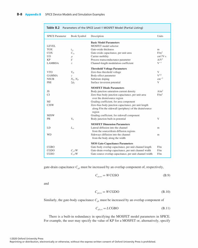
MOSFET Model Parameters Table B.2 provides a listing of some of the MOSFETmodel parameters used in the level-1 model. The reader should already be familiar withthese parameters, except for a few, which are described next.
MOSFET Diode Parameters For the two reverse-biased diodes formed between each ofthe source and drain diffusion regions and the body (see Fig. 10.3), the saturation-currentdensity is modeled in SPICE by the parameter JS. Furthermore, based on the parametersspecified in Table B.2, SPICE will calculate the depletion-layer ( junction) capacitancesdiscussed in Section 10.1.1 as
Cdb = CJ(1+ VDB
PB
)MJ AD+ CJSW(1+ VDB
PB
)MJSW PD (B.5)
Csb = CJ(1+ VSB
PB
)MJ AS+ CJSW(1+ VSB
PB
)MJSW PS (B.6)
where AD and AS are the areas, and PD and PS are the perimeters of, respectively, thedrain and source regions of the MOSFET. The first capacitance term in Eqs. (B.5) and (B.6)represents the depletion-layer (junction) capacitance over the bottom of the drain and sourceregions. The second capacitance term accounts for the depletion-layer capacitance along thesidewall (periphery) of these regions. Both terms are expressed using the formula developedin Section 3.6.1 (Eq. 3.47). The values of AD, AS, PD, and PS must be specified by the userbased on the dimensions of the device being used.
MOSFET Dimension and Gate-Capacitance Parameters In a fabricated MOSFET,the effective channel length Leff is shorter than the nominal (or drawn) channel length L (asspecified by the designer) because the source and drain diffusion regions extend slightlyunder the gate oxide during fabrication. Furthermore, the effective channel width Weff ofthe MOSFET is shorter than the nominal or drawn channel widthW because of the sidewaysdiffusion into the channel from the body along the width. In terms of the parameters specifiedin Table B.2,
Leff = L− 2LD (B.7)
Weff =W− 2WD (B.8)
In a manner analogous to using Lov to denote LD, we will use the symbol Wov to denoteWD. Consequently, as indicated in Section 10.1.1, the gate-source capacitance Cgs and the
©20 Oxford University PressReprinting or distribution, electronically or otherwise, without the express written consent of Oxford University Press is prohibited.
20
B-8 Appendix B SPICE Device Models and Simulation Examples
Table B.2 Parameters of the SPICE Level-1 MOSFET Model (Partial Listing)
SPICE Parameter Book Symbol Description Units
Basic Model ParametersLEVEL MOSFET model selectorTOX tox Gate-oxide thickness mCOX Cox Gate-oxide capacitance, per unit area F/m2
UO μ Carrier mobility cm2/V·sKP k ′ Process transconductance parameter A/V2
LAMBDA λ Channel-length modulation coefficient V−1
Threshold Voltage ParametersVTO Vt0 Zero-bias threshold voltage VGAMMA γ Body-effect parameter V1/2
NSUB NA, ND Substrate doping cm−3
PHI 2φf Surface inversion potential V
MOSFET Diode ParametersJS Body-junction saturation-current density A/m2
CJ Zero-bias body-junction capacitance, per unit area F/m2
over the drain/source regionMJ Grading coefficient, for area componentCJSW Zero-bias body-junction capacitance, per unit length
along F/m the sidewall (periphery) of the drain/sourceregion
MJSW Grading coefficient, for sidewall componentPB V0 Body-junction built-in potential V
MOSFET Dimension ParametersLD Lov Lateral diffusion into the channel m
from the source/drain diffusion regionsWD Sideways diffusion into the channel m
from the body along the width
MOS Gate-Capacitance ParametersCGBO Gate-body overlap capacitance, per unit channel length F/mCGDO Cov/W Gate-drain overlap capacitance, per unit channel width F/mCGSO Cov/W Gate-source overlap capacitance, per unit channel width F/m
gate-drain capacitance Cgd must be increased by an overlap component of, respectively,
Cgs,ov =WCGSO (B.9)
and
Cgd,ov =WCGDO (B.10)
Similarly, the gate-body capacitance Cgb must be increased by an overlap component of
Cgb,ov = LCGBO (B.11)
There is a built-in redundancy in specifying the MOSFET model parameters in SPICE.For example, the user may specify the value of KP for a MOSFET or, alternatively, specify
©20 Oxford University PressReprinting or distribution, electronically or otherwise, without the express written consent of Oxford University Press is prohibited.
20
B.1 SPICE Device Models B-9
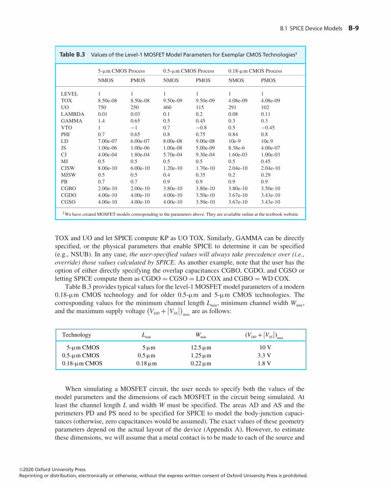
Table B.3 Values of the Level-1 MOSFETModel Parameters for Exemplar CMOS Technologies1
5-µm CMOS Process 0.5-µm CMOS Process 0.18-µm CMOS Process
NMOS PMOS NMOS PMOS NMOS PMOS
LEVEL 1 1 1 1 1 1TOX 8.50e-08 8.50e-08 9.50e-09 9.50e-09 4.08e-09 4.08e-09UO 750 250 460 115 291 102LAMBDA 0.01 0.03 0.1 0.2 0.08 0.11GAMMA 1.4 0.65 0.5 0.45 0.3 0.3VTO 1 −1 0.7 −0.8 0.5 −0.45PHI 0.7 0.65 0.8 0.75 0.84 0.8LD 7.00e-07 6.00e-07 8.00e-08 9.00e-08 10e-9 10e.9JS 1.00e-06 1.00e-06 1.00e-08 5.00e-09 8.38e-6 4.00e-07CJ 4.00e-04 1.80e-04 5.70e-04 9.30e-04 1.60e-03 1.00e-03MJ 0.5 0.5 0.5 0.5 0.5 0.45CJSW 8.00e-10 6.00e-10 1.20e-10 1.70e-10 2.04e-10 2.04e-10MJSW 0.5 0.5 0.4 0.35 0.2 0.29PB 0.7 0.7 0.9 0.9 0.9 0.9CGBO 2.00e-10 2.00e-10 3.80e-10 3.80e-10 3.80e-10 3.50e-10CGDO 4.00e-10 4.00e-10 4.00e-10 3.50e-10 3.67e-10 3.43e-10CGSO 4.00e-10 4.00e-10 4.00e-10 3.50e-10 3.67e-10 3.43e-10
1We have created MOSFET models corresponding to the parameters above. They are available online at the textbook website.
TOX and UO and let SPICE compute KP as UO TOX. Similarly, GAMMA can be directlyspecified, or the physical parameters that enable SPICE to determine it can be specified(e.g., NSUB). In any case, the user-specified values will always take precedence over (i.e.,override) those values calculated by SPICE. As another example, note that the user has theoption of either directly specifying the overlap capacitances CGBO, CGDO, and CGSO orletting SPICE compute them as CGDO = CGSO = LD COX and CGBO = WD COX.
Table B.3 provides typical values for the level-1 MOSFETmodel parameters of a modern0.18-µm CMOS technology and for older 0.5-µm and 5-µm CMOS technologies. Thecorresponding values for the minimum channel length Lmin, minimum channel width Wmin,and the maximum supply voltage
(VDD + ∣∣VSS∣∣)max
are as follows:
Technology Lmin Wmin (VDD + ∣∣VSS
∣∣)max
5-µm CMOS 5µm 12.5µm 10 V0.5-µm CMOS 0.5µm 1.25µm 3.3 V0.18-µm CMOS 0.18µm 0.22µm 1.8 V
When simulating a MOSFET circuit, the user needs to specify both the values of themodel parameters and the dimensions of each MOSFET in the circuit being simulated. Atleast the channel length L and width W must be specified. The areas AD and AS and theperimeters PD and PS need to be specified for SPICE to model the body-junction capaci-tances (otherwise, zero capacitances would be assumed). The exact values of these geometryparameters depend on the actual layout of the device (Appendix A). However, to estimatethese dimensions, we will assume that a metal contact is to be made to each of the source and
©20 Oxford University PressReprinting or distribution, electronically or otherwise, without the express written consent of Oxford University Press is prohibited.
20
B-10 Appendix B SPICE Device Models and Simulation Examples
drain regions of the MOSFET. For this purpose, typically, these diffusion regions must beextended past the end of the channel (i.e., in the L-direction in Fig. 5.1) by at least 2.75 Lmin.Thus, the minimum area and perimeter of a drain/source diffusion region with a contact are,respectively,
AD=AS= 2.75LminW (B.12)
and
PD= PS= 2× 2.75Lmin +W (B.13)
Unless otherwise specified, we will use Eqs. (B.12) and (B.13) to estimate the dimensions ofthe drain/source regions in our examples.
Finally, we note that SPICE computes the values for the parameters of the MOSFETsmall-signal model based on the dc operating point (bias point). These are then used bySPICE to perform the small-signal analysis (called “ac analysis”).
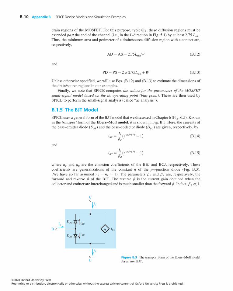
B.1.5 The BJT Model
SPICE uses a general form of the BJTmodel that we discussed in Chapter 6 (Fig. 6.5). Knownas the transport form of the Ebers–Moll model, it is shown in Fig. B.5. Here, the currents ofthe base–emitter diode (DBE) and the base–collector diode (DBC) are given, respectively, by
iBE = ISβF
(evBE /nFVT − 1
)(B.14)
and
iBC = ISβR
(evBC /nRVT − 1
)(B.15)
where nF and nR are the emission coefficients of the BEJ and BCJ, respectively. Thesecoefficients are generalizations of the constant n of the pn-junction diode (Fig. B.3).(We have so far assumed nF = nR = 1). The parameters βF and βR are, respectively, theforward and reverse β of the BJT. The reverse β is the current gain obtained when thecollector and emitter are interchanged and is much smaller than the forward β. In fact, βR�1.
iCE
DBC
B
E
C
iB
iE
DBE
iBC
iBE
iC
Figure B.5 The transport form of the Ebers–Moll modelfor an npn BJT.
©20 Oxford University PressReprinting or distribution, electronically or otherwise, without the express written consent of Oxford University Press is prohibited.
20
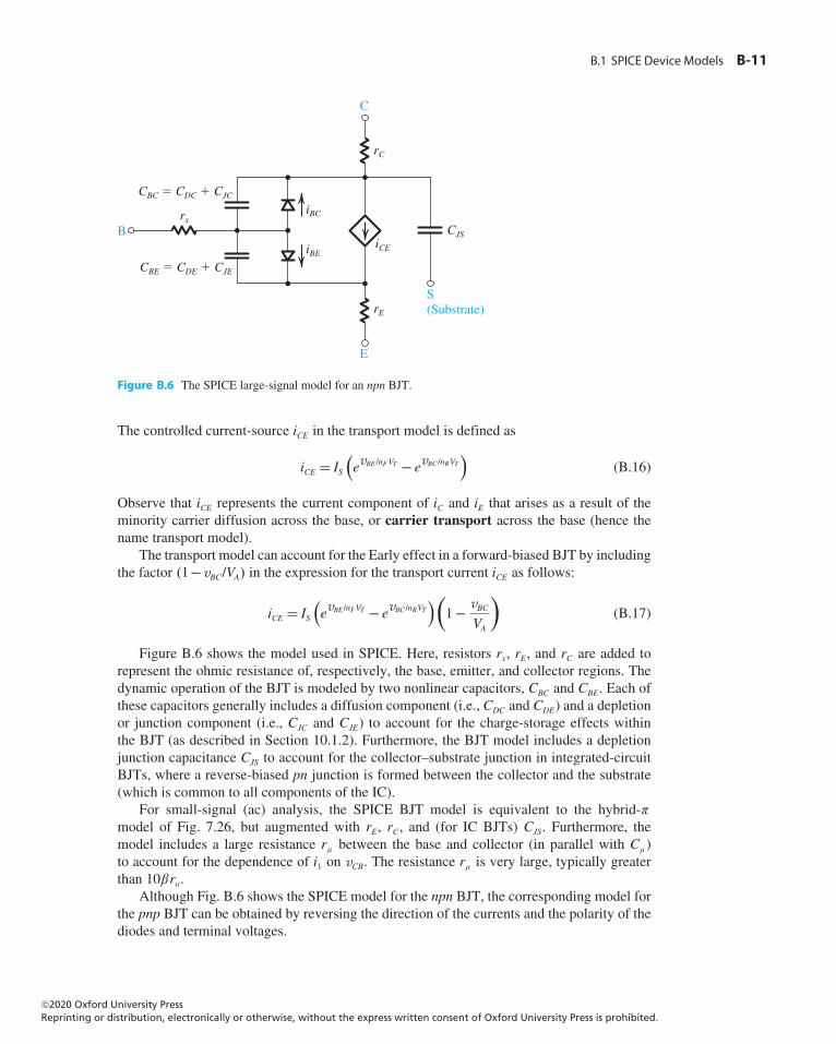
B.1 SPICE Device Models B-11
iCE
CJS
CBC � CDC � CJC
CBE � CDE � CJE
B
E
S(Substrate)
iBC
iBE
rC
C
rx
rE
Figure B.6 The SPICE large-signal model for an npn BJT.
The controlled current-source iCE in the transport model is defined as
iCE = IS(evBE /nFVT − evBC /nRVT
)(B.16)
Observe that iCE represents the current component of iC and iE that arises as a result of theminority carrier diffusion across the base, or carrier transport across the base (hence thename transport model).
The transport model can account for the Early effect in a forward-biased BJT by includingthe factor (1−vBC/VA) in the expression for the transport current iCE as follows:
iCE = IS(evBE /nFVT − evBC /nRVT
)(1− vBC
VA
)(B.17)
Figure B.6 shows the model used in SPICE. Here, resistors rx, rE, and rC are added torepresent the ohmic resistance of, respectively, the base, emitter, and collector regions. Thedynamic operation of the BJT is modeled by two nonlinear capacitors, CBC and CBE. Each ofthese capacitors generally includes a diffusion component (i.e., CDC and CDE) and a depletionor junction component (i.e., CJC and CJE) to account for the charge-storage effects withinthe BJT (as described in Section 10.1.2). Furthermore, the BJT model includes a depletionjunction capacitance CJS to account for the collector–substrate junction in integrated-circuitBJTs, where a reverse-biased pn junction is formed between the collector and the substrate(which is common to all components of the IC).
For small-signal (ac) analysis, the SPICE BJT model is equivalent to the hybrid-πmodel of Fig. 7.26, but augmented with rE, rC, and (for IC BJTs) CJS. Furthermore, themodel includes a large resistance rμ between the base and collector (in parallel with Cμ)to account for the dependence of i1 on vCB. The resistance rμ is very large, typically greaterthan 10βro.
Although Fig. B.6 shows the SPICE model for the npn BJT, the corresponding model forthe pnp BJT can be obtained by reversing the direction of the currents and the polarity of thediodes and terminal voltages.
©20 Oxford University PressReprinting or distribution, electronically or otherwise, without the express written consent of Oxford University Press is prohibited.
20
B-12 Appendix B SPICE Device Models and Simulation Examples
The SPICE Gummel–Poon Model of the BJT The BJT model described above lacksa representation of some second-order effects present in actual devices. One of the mostimportant such effects is the variation of the current gains, βF and βR, with the current iC.The Ebers–Moll model assumes βF and βR to be constant, thereby neglecting their currentdependence (as depicted in Fig. 6.20). To account for this, and other second-order effects,SPICE uses a more accurate, yet more complex, BJT model called the Gummel–Poon model(named after H. K. Gummel and H. C. Poon, two pioneers in this field). This model isbased on the relationship between the electrical terminal characteristics of a BJT and itsbase charge. It is beyond the scope of this book to delve into the model details. However, itis important for the reader to be aware of the existence of such a model.
In SPICE, the Gummel–Poon model automatically simplifies to the Ebers–Moll modelwhen certain model parameters are not specified. Consequently, the BJT model to be usedby SPICE need not be explicitly specified by the user (unlike the MOSFET case in whichthe model is specified by the LEVEL parameter). For discrete BJTs, the values of theSPICE model parameters can be determined from the data specified on the BJT data sheets,supplemented (if needed) by key measurements. For instance, in Example S.6.1, we willuse the Q2N3904 npn BJT (from Fairchild Semiconductor) whose SPICE model is readilyavailable. In fact, most SPICE simulators already include the SPICE model parameters formany of the commercially available discrete BJTs. For IC BJTs, the values of the SPICEmodel parameters are determined by the IC manufacturer (using both measurements on thefabricated devices and knowledge of the details of the fabrication process) and are providedto IC designers.
The SPICE BJT Model Parameters Table B.4 provides a listing of some of theBJT model parameters used in SPICE. The reader should be already familiar with theseparameters. In the absence of a user-specified value for a particular parameter, SPICE usesa default value that typically results in the corresponding effect being ignored. For example,if no value is specified for the forward Early voltage (VAF), SPICE assumes that VAF=∞and does not account for the Early effect. Although ignoring VAF can be a serious issuein some circuits, the same is not true, for example, for the value of the reverse Earlyvoltage (VAR).
The BJT Model Parameters BF and BR in SPICE Before leaving the SPICE model, acomment on β is in order. SPICE interprets the user-specified model parameters BF and BRas the ideal maximum values of the forward and reverse dc current gains, respectively, versusthe operating current. These parameters are not equal to the constant-current-independentparameters βF(βdc) and βR used in the Ebers–Moll model for the forward and reverse dccurrent gains of the BJT. SPICE uses a current-dependent model for βF and βR, and theuser can specify other parameters (not shown in Table B.4) for this model. Only when suchparameters are not specified, and the Early effect is neglected, will SPICE assume that βF
and βR are constant and equal to BF and BR, respectively. Furthermore, SPICE computesvalues for both βdc and βac, the two parameters that we generally assume to be approximatelyequal. SPICE then uses βac to perform small-signal (ac) analysis.
©20 Oxford University PressReprinting or distribution, electronically or otherwise, without the express written consent of Oxford University Press is prohibited.
20
B.2 SPICE Examples B-13
Table B.4 Parameters of the SPICE BJT Model (Partial Listing)
SPICE BookParameter Symbol Description Units
IS IS Saturation current ABF βF Ideal maximum forward current gainBR βR Ideal maximum reverse current gainNF nF Forward current emission coefficientNR nR Reverse current emission coefficientVAF VA Forward Early voltage VVAR Reverse Early voltage VRB rx Zero-bias base ohmic resistance �
RC rC Collector ohmic resistance �
RE rE Emitter ohmic resistance �
TF τ F Ideal forward transit time sTR τ R Ideal reverse transit time sCJC Cμ0 Zero-bias base–collector depletion F
( junction) capacitanceMJC mBCJ Base–collector grading coefficientVJC V0c Base–collector built-in potential VCJE Cje0 Zero-bias base–emitter depletion F
( junction) capacitanceMJE mBEJ Base–emitter grading coefficientVJE V0e Base–emitter built-in potential VCJS Zero-bias collector–substrate depletion F
( junction) capacitanceMJS Collector–substrate grading coefficientVJS Collector–substrate built-in potential V
B.2 SPICE Examples
Example S.2.1
Performance of a Noninverting AmplifierConsider an op amp with a differential input resistance of 2 M�, an input offset voltage of 1 mV, a dcgain of 100 dB, and an output resistance of 75�. Assume the op amp is internally compensated and hasan STC frequency response with a gain–bandwidth product of 1 MHz.
(a) Create a subcircuit model for this op amp in SPICE.(b) Using this subcircuit, simulate the closed-loop noninverting amplifier in Fig. 2.12 with resistors R1 =
1 k� and R2 = 100 k� to find:(i) Its 3-dB bandwidth f3dB.(ii) Its output offset voltage VOSout.(iii) Its input resistance Rin.(iv) Its output resistance Rout.
(c) Simulate the step response of the closed-loop amplifier, and measure its rise time tr. Verify that thistime agrees with the 3-dB frequency measured above.
©20 Oxford University PressReprinting or distribution, electronically or otherwise, without the express written consent of Oxford University Press is prohibited.
20
B-14 Appendix B SPICE Device Models and Simulation Examples
Example S.2.1 continued
Solution
To model the op amp in SPICE, we use the equivalent circuit in Fig. B.2, but with Rid = 2 M�, Ricm = ∞(open circuit), IB1 = IB2 = 0 (open circuit), VOS = 1 mV, A0d = 105 V/V, A0cm = 0 (short circuit), andRo = 75�. Furthermore, we set Cb = 1 µF and Rb = 15.915 k� to achieve an ft = 1 MHz.
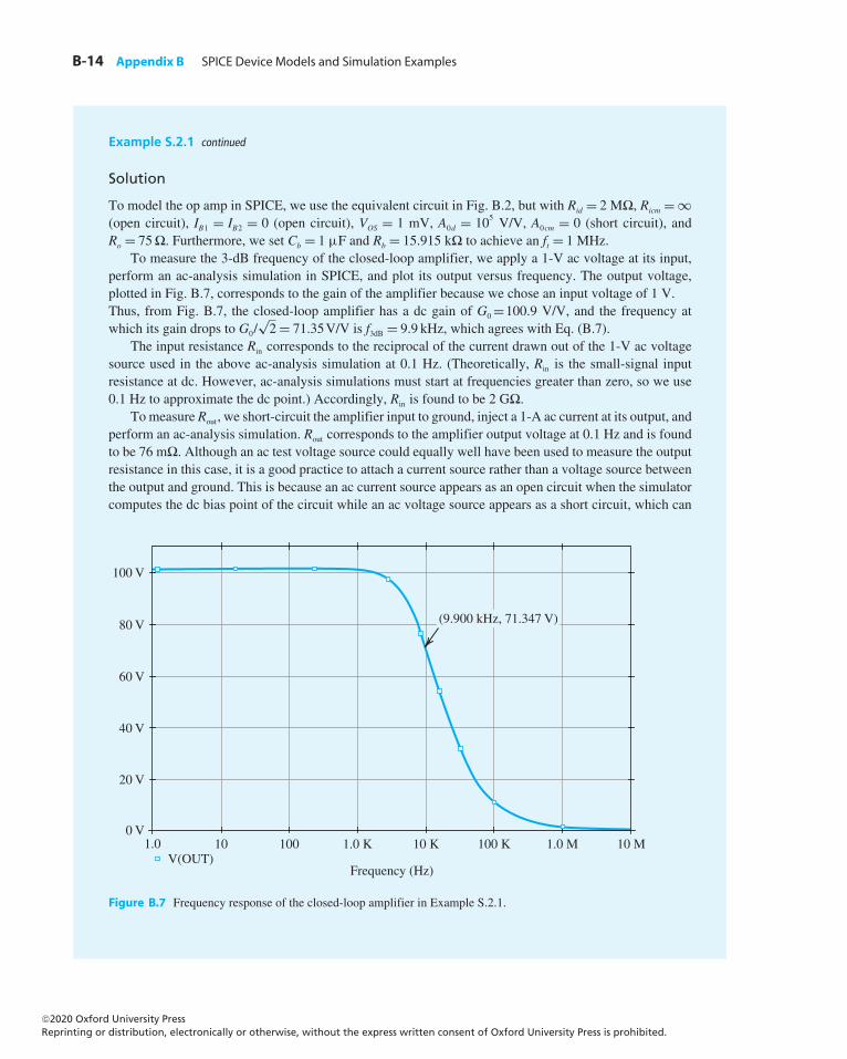
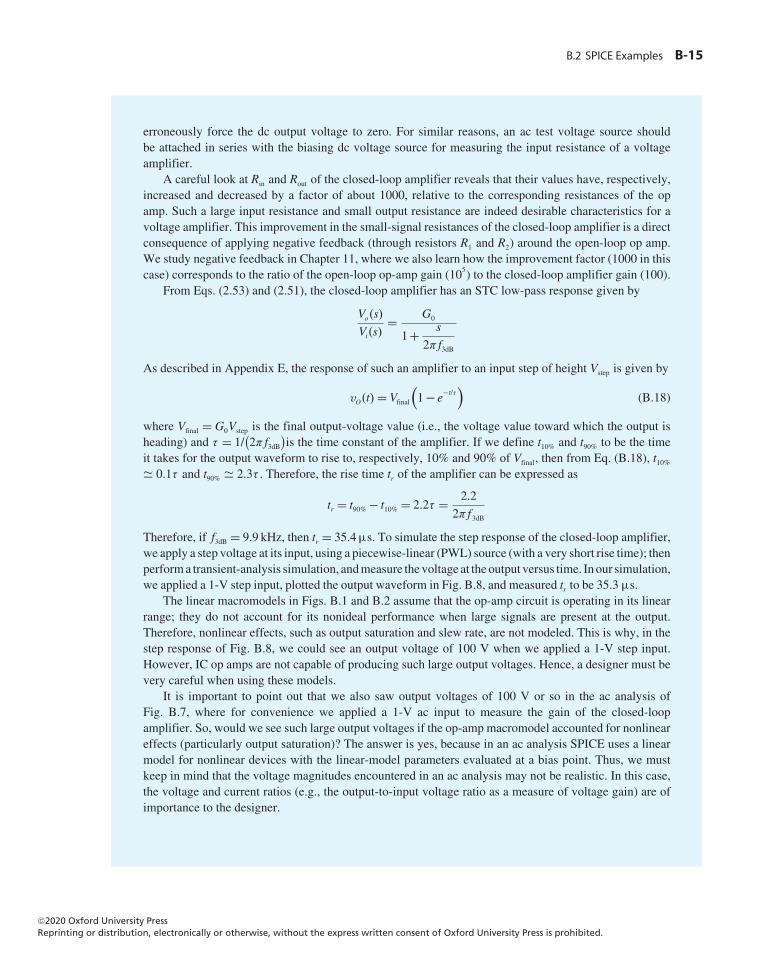
To measure the 3-dB frequency of the closed-loop amplifier, we apply a 1-V ac voltage at its input,perform an ac-analysis simulation in SPICE, and plot its output versus frequency. The output voltage,plotted in Fig. B.7, corresponds to the gain of the amplifier because we chose an input voltage of 1 V.Thus, from Fig. B.7, the closed-loop amplifier has a dc gain of G0 =100.9 V/V, and the frequency atwhich its gain drops to G0/
√2= 71.35V/V is f3dB = 9.9 kHz, which agrees with Eq. (B.7).
The input resistance Rin corresponds to the reciprocal of the current drawn out of the 1-V ac voltagesource used in the above ac-analysis simulation at 0.1 Hz. (Theoretically, Rin is the small-signal inputresistance at dc. However, ac-analysis simulations must start at frequencies greater than zero, so we use0.1 Hz to approximate the dc point.) Accordingly, Rin is found to be 2 G�.
To measure Rout, we short-circuit the amplifier input to ground, inject a 1-A ac current at its output, andperform an ac-analysis simulation. Rout corresponds to the amplifier output voltage at 0.1 Hz and is foundto be 76 m�. Although an ac test voltage source could equally well have been used to measure the outputresistance in this case, it is a good practice to attach a current source rather than a voltage source betweenthe output and ground. This is because an ac current source appears as an open circuit when the simulatorcomputes the dc bias point of the circuit while an ac voltage source appears as a short circuit, which can
0 V
20 V
40 V
60 V
80 V
1.0 10 100 1.0 K
Frequency (Hz)
10 K 100 K 1.0 M 10 M
100 V
V(OUT)
(9.900 kHz, 71.347 V)
Figure B.7 Frequency response of the closed-loop amplifier in Example S.2.1.
©20 Oxford University PressReprinting or distribution, electronically or otherwise, without the express written consent of Oxford University Press is prohibited.
20
B.2 SPICE Examples B-15
erroneously force the dc output voltage to zero. For similar reasons, an ac test voltage source shouldbe attached in series with the biasing dc voltage source for measuring the input resistance of a voltageamplifier.
A careful look at Rin and Rout of the closed-loop amplifier reveals that their values have, respectively,increased and decreased by a factor of about 1000, relative to the corresponding resistances of the opamp. Such a large input resistance and small output resistance are indeed desirable characteristics for avoltage amplifier. This improvement in the small-signal resistances of the closed-loop amplifier is a directconsequence of applying negative feedback (through resistors R1 and R2) around the open-loop op amp.We study negative feedback in Chapter 11, where we also learn how the improvement factor (1000 in thiscase) corresponds to the ratio of the open-loop op-amp gain (105) to the closed-loop amplifier gain (100).
From Eqs. (2.53) and (2.51), the closed-loop amplifier has an STC low-pass response given by
Vo(s)
Vi(s)= G0
1+ s
2π f3dB
As described in Appendix E, the response of such an amplifier to an input step of height Vstep is given by
vO(t) = Vfinal
(1− e−t/τ
)(B.18)
where Vfinal = G0Vstep is the final output-voltage value (i.e., the voltage value toward which the output isheading) and τ = 1/
(2π f3dB
)is the time constant of the amplifier. If we define t10% and t90% to be the time
it takes for the output waveform to rise to, respectively, 10% and 90% of Vfinal, then from Eq. (B.18), t10%
� 0.1τ and t90% � 2.3τ . Therefore, the rise time tr of the amplifier can be expressed as
tr = t90% − t10% = 2.2τ = 2.2
2π f3dB
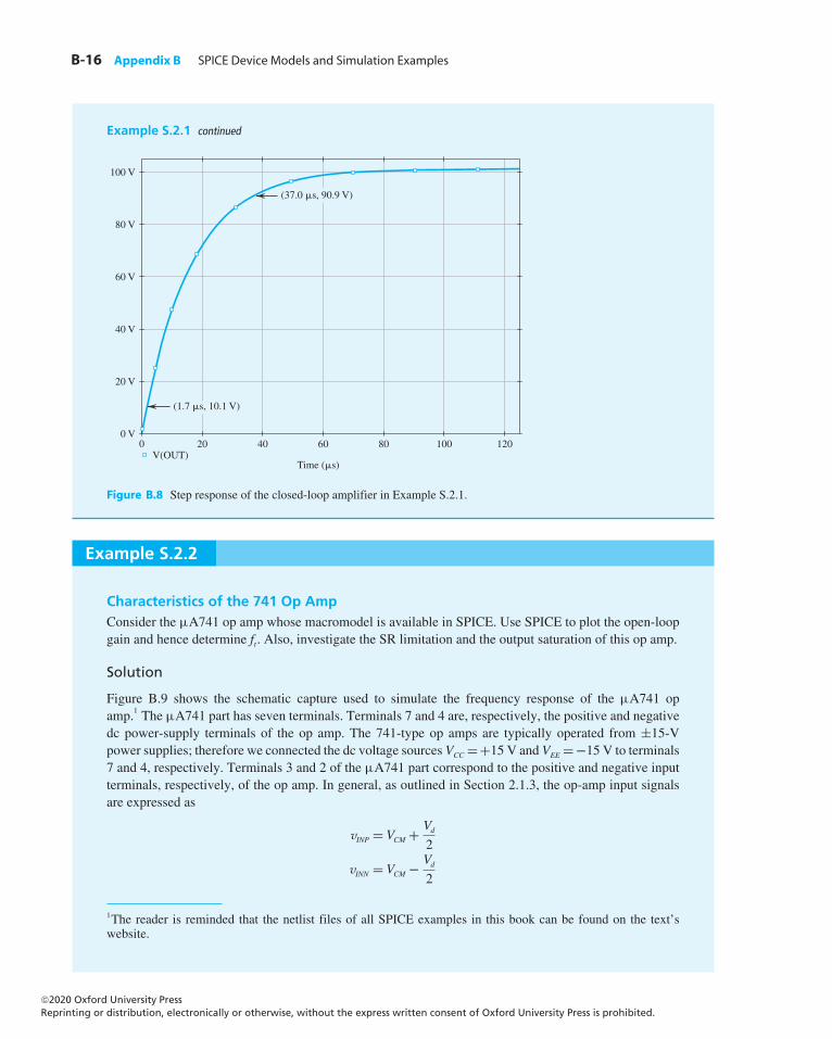
Therefore, if f3dB = 9.9 kHz, then tr = 35.4µs. To simulate the step response of the closed-loop amplifier,we apply a step voltage at its input, using a piecewise-linear (PWL) source (with a very short rise time); thenperforma transient-analysis simulation, andmeasure thevoltage at the output versus time. In our simulation,we applied a 1-V step input, plotted the output waveform in Fig. B.8, and measured tr to be 35.3 µs.
The linear macromodels in Figs. B.1 and B.2 assume that the op-amp circuit is operating in its linearrange; they do not account for its nonideal performance when large signals are present at the output.Therefore, nonlinear effects, such as output saturation and slew rate, are not modeled. This is why, in thestep response of Fig. B.8, we could see an output voltage of 100 V when we applied a 1-V step input.However, IC op amps are not capable of producing such large output voltages. Hence, a designer must bevery careful when using these models.
It is important to point out that we also saw output voltages of 100 V or so in the ac analysis ofFig. B.7, where for convenience we applied a 1-V ac input to measure the gain of the closed-loopamplifier. So, would we see such large output voltages if the op-amp macromodel accounted for nonlineareffects (particularly output saturation)? The answer is yes, because in an ac analysis SPICE uses a linearmodel for nonlinear devices with the linear-model parameters evaluated at a bias point. Thus, we mustkeep in mind that the voltage magnitudes encountered in an ac analysis may not be realistic. In this case,the voltage and current ratios (e.g., the output-to-input voltage ratio as a measure of voltage gain) are ofimportance to the designer.
©20 Oxford University PressReprinting or distribution, electronically or otherwise, without the express written consent of Oxford University Press is prohibited.
20
B-16 Appendix B SPICE Device Models and Simulation Examples
Example S.2.1 continued
0 20 40 60
Time (�s)
80 100 1200 V
20 V
40 V
60 V
80 V
100 V
V(OUT)
(37.0 �s, 90.9 V)
(1.7 �s, 10.1 V)
Figure B.8 Step response of the closed-loop amplifier in Example S.2.1.
Example S.2.2
Characteristics of the 741 Op AmpConsider the µA741 op amp whose macromodel is available in SPICE. Use SPICE to plot the open-loopgain and hence determine ft. Also, investigate the SR limitation and the output saturation of this op amp.
Solution
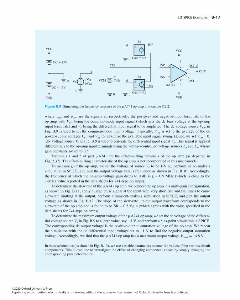
Figure B.9 shows the schematic capture used to simulate the frequency response of the µA741 opamp.1 The µA741 part has seven terminals. Terminals 7 and 4 are, respectively, the positive and negativedc power-supply terminals of the op amp. The 741-type op amps are typically operated from ±15-Vpower supplies; therefore we connected the dc voltage sources VCC =+15 V and VEE =−15 V to terminals7 and 4, respectively. Terminals 3 and 2 of the µA741 part correspond to the positive and negative inputterminals, respectively, of the op amp. In general, as outlined in Section 2.1.3, the op-amp input signalsare expressed as
vINP = VCM + Vd2
vINN = VCM − Vd2
1The reader is reminded that the netlist files of all SPICE examples in this book can be found on the text’swebsite.
©20 Oxford University PressReprinting or distribution, electronically or otherwise, without the express written consent of Oxford University Press is prohibited.
20
B.2 SPICE Examples B-17
VEE
0
VCC
d
Vd1Vac0Vdc
DC � 15V
DC � 15V
0 �
�
d INPEp
�
�
��
End
CM
VCM 0Vdc
INN
0
00Gain � 0.5
�
�
��
�
�
Gain � 0.5
�
�
INP 3
uA741
2INN
7
4
VCC
VEE
V�
V�
5
6
1
OS2
OS1
OUT
Figure B.9 Simulating the frequency response of the µA741 op-amp in Example S.2.2.
where vINP and vINN are the signals at, respectively, the positive- and negative-input terminals of theop amp with VCM being the common-mode input signal (which sets the dc bias voltage at the op-ampinput terminals) and Vd being the differential input signal to be amplified. The dc voltage source VCM inFig. B.9 is used to set the common-mode input voltage. Typically, VCM is set to the average of the dcpower-supply voltages VCC and VEE to maximize the available input signal swing. Hence, we set VCM =0.The voltage source Vd in Fig. B.9 is used to generate the differential input signal Vd. This signal is applieddifferentially to the op-amp input terminals using the voltage-controlled voltage sources Ep and En, whosegain constants are set to 0.5.
Terminals 1 and 5 of part µA741 are the offset-nulling terminals of the op amp (as depicted inFig. 2.37). The offset-nulling characteristic of the op amp is not incorporated in this macromodel.
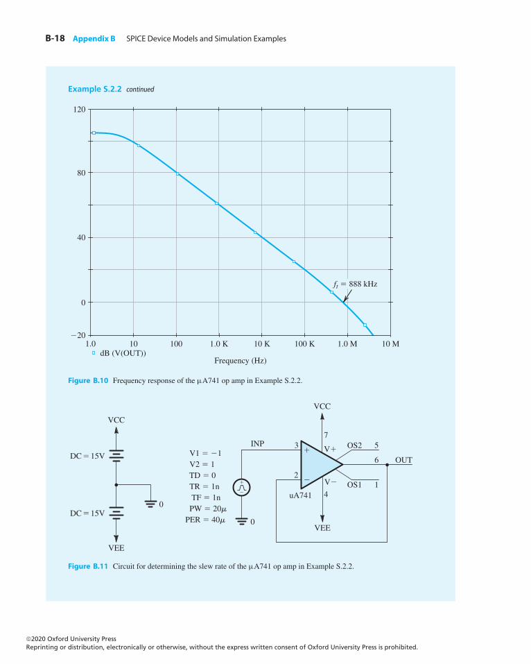
To measure ft of the op amp, we set the voltage of source Vd to be 1-V ac, perform an ac-analysissimulation in SPICE, and plot the output voltage versus frequency as shown in Fig. B.10. Accordingly,the frequency at which the op-amp voltage gain drops to 0 dB is ft = 0.9 MHz (which is close to the1-MHz value reported in the data sheets for 741-type op amps).
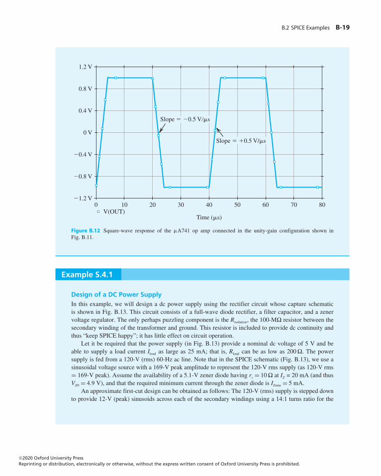
To determine the slew rate of theµA741 op amp, we connect the op amp in a unity-gain configuration,as shown in Fig. B.11, apply a large pulse signal at the input with very short rise and fall times to causeslew-rate limiting at the output, perform a transient-analysis simulation in SPICE, and plot the outputvoltage as shown in Fig. B.12. The slope of the slew-rate limited output waveform corresponds to theslew-rate of the op amp and is found to be SR = 0.5 V/µs (which agrees with the value specified in thedata sheets for 741-type op amps).
To determine the maximum output voltage of theµA741 op amp, we set the dc voltage of the differen-tial voltage source Vd in Fig. B.9 to a large value, say+1 V, and perform a bias-point simulation in SPICE.The corresponding dc output voltage is the positive-output saturation voltage of the op amp. We repeatthe simulation with the dc differential input voltage set to –1 V to find the negative-output saturationvoltage. Accordingly, we find that the µA741 op amp has a maximum output voltage Vomax = 14.8 V.
In these schematics (as shown in Fig. B.13), we use variable parameters to enter the values of the various circuitcomponents. This allows one to investigate the effect of changing component values by simply changing thecorresponding parameter values.
©20 Oxford University PressReprinting or distribution, electronically or otherwise, without the express written consent of Oxford University Press is prohibited.
20
B-18 Appendix B SPICE Device Models and Simulation Examples
Example S.2.2 continued
�20
0
40
80
120
1.0 10 100 1.0 K
Frequency (Hz)
10 K 100 K 1.0 M 10 MdB (V(OUT))
ft � 888 kHz
Figure B.10 Frequency response of the µA741 op amp in Example S.2.2.
Figure B.11 Circuit for determining the slew rate of the µA741 op amp in Example S.2.2.
©20 Oxford University PressReprinting or distribution, electronically or otherwise, without the express written consent of Oxford University Press is prohibited.
20
B.2 SPICE Examples B-19
�1.2 V
�0.8 V
�0.4 V
0 V
0.4 V
0.8 V
0 10 20 30 40
Time (�s)
50 7060 80
1.2 V
Slope � �0.5 V��s
Slope � �0.5 V/�s
V(OUT)
Figure B.12 Square-wave response of the µA741 op amp connected in the unity-gain configuration shown inFig. B.11.
Example S.4.1
Design of a DC Power SupplyIn this example, we will design a dc power supply using the rectifier circuit whose capture schematicis shown in Fig. B.13. This circuit consists of a full-wave diode rectifier, a filter capacitor, and a zenervoltage regulator. The only perhaps puzzling component is the Risolation, the 100-M� resistor between thesecondary winding of the transformer and ground. This resistor is included to provide dc continuity andthus “keep SPICE happy”; it has little effect on circuit operation.
Let it be required that the power supply (in Fig. B.13) provide a nominal dc voltage of 5 V and beable to supply a load current Iload as large as 25 mA; that is, Rload can be as low as 200�. The powersupply is fed from a 120-V (rms) 60-Hz ac line. Note that in the SPICE schematic (Fig. B.13), we use asinusoidal voltage source with a 169-V peak amplitude to represent the 120-V rms supply (as 120-V rms= 169-V peak). Assume the availability of a 5.1-V zener diode having rz = 10� at IZ = 20 mA (and thusVZ0 = 4.9 V), and that the required minimum current through the zener diode is IZmin = 5 mA.
An approximate first-cut design can be obtained as follows: The 120-V (rms) supply is stepped downto provide 12-V (peak) sinusoids across each of the secondary windings using a 14:1 turns ratio for the
©20 Oxford University PressReprinting or distribution, electronically or otherwise, without the express written consent of Oxford University Press is prohibited.
20
B-20 Appendix B SPICE Device Models and Simulation Examples
Example S.4.1 continued
PARAMETERS: C � 520u
R � 191Risolation � 100E6 Rload � 200 Rs � 0.5
3
21
76
4
0
Vsin
{Rload}Zener_diode
{Risolation}
Ls1
Ls2Lp
{R}
{C}
D1
D1N4148
5 D2
D1N4148
00
{Rs}
�
�
VOFF � 0VAMPL � 169 FREQ � 60
Figure B.13 Schematic capture of the 5-V dc power supply in Example S.4.1.
center-tapped transformer. The choice of 12 V is a reasonable compromise between the need to allow forsufficient voltage (above the 5-V output) to operate the rectifier and the regulator, while keeping the PIVratings of the diodes reasonably low. To determine a value for R, we can use the following expression:
R= VCmin −VZ0 − rzIZmin
IZmin + ILmax
where an estimate for VCmin, the minimum voltage across the capacitor, can be obtained by subtracting adiode drop (say, 0.8 V) from 12 V and allowing for a ripple voltage across the capacitor of, say, Vr =0.5 V.Thus, VS min =10.7 V. Furthermore, we note that IL max =25 mA and IZmin =5 mA, and that VZ0=4.9 V andrz=10�. The result is that R= 191 �.
Next, we determine C using a restatement of Eq. (4.33) with Vp /R replaced by the current throughthe 191-� resistor. This current can be estimated by noting that the voltage across C varies from 10.7 Vto 11.2 V, and thus has an average value of 10.95 V. Furthermore, the desired voltage across the zener is5 V. The result is C= 520µF.
Now, with an approximate design in hand, we can proceed with the SPICE simulation. For the zenerdiode, we use the model of Fig. B.4, and assume (arbitrarily) thatD1 has IS =100 pA and n=0.01 whileD2
has IS=100 pA and n=1.7. For the rectifier diodes, we use the commercially available 1N4148 type (withIS=2.682 nA, n=1.836, RS=0.5664�, V0 =0.5 V, Cj0 =4 pF, m=0.333, τ T =11.54 ns, VZK =100 V,IZK =100 µA).
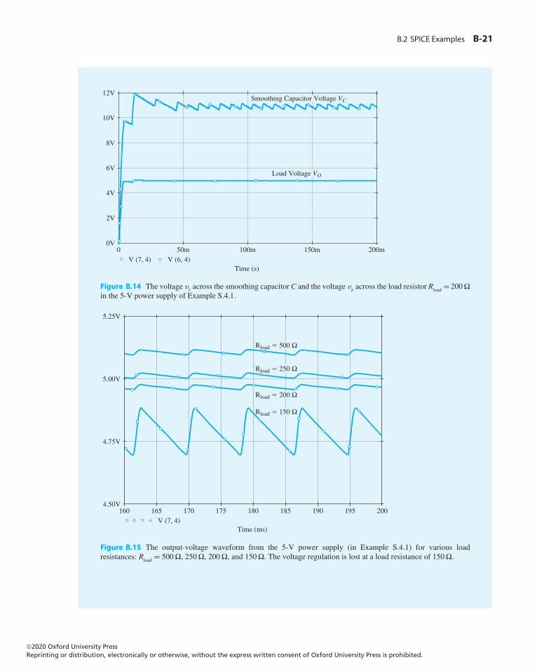
In SPICE, we perform a transient analysis and plot the waveforms of both the voltage vC acrossthe smoothing capacitor C and the voltage vO across the load resistor Rload. The simulation results forRload = 200� (Iload � 25 mA) are presented in Fig. B.14. Observe that vC has an average of 10.85 V anda ripple of ± 0.21 V. Thus, V1 = 0.42 V, which is close to the 0.5-V value that we would expect fromthe chosen value of C. The output voltage vO is very close to the required 5 V, with vO varying between4.957 V and 4.977 V for a ripple of only 20 mV. The variations of vO with Rload are illustrated in Fig. B.15
©20 Oxford University PressReprinting or distribution, electronically or otherwise, without the express written consent of Oxford University Press is prohibited.
20
B.2 SPICE Examples B-21
Time (s)
0 50m 100m 150m 200m0V
2V
4V
6V
8V
10V
12VSmoothing Capacitor Voltage VC
Load Voltage VO
V (7, 4) V (6, 4)
Figure B.14 The voltage vc across the smoothing capacitor C and the voltage vo across the load resistor Rload = 200�in the 5-V power supply of Example S.4.1.
Rload � 150 Ω
Time (ms)
160 165 170 175 180 185 190 195 2004.50V
4.75V
5.00V
5.25V
V (7, 4)
Rload � 500 Ω
Rload � 250 Ω
Rload � 200 Ω
Figure B.15 The output-voltage waveform from the 5-V power supply (in Example S.4.1) for various loadresistances: Rload = 500�, 250�, 200�, and 150�. The voltage regulation is lost at a load resistance of 150�.
©20 Oxford University PressReprinting or distribution, electronically or otherwise, without the express written consent of Oxford University Press is prohibited.
20
B-22 Appendix B SPICE Device Models and Simulation Examples
Example S.4.1 continued
for Rload = 500�, 250�, 200 �, and 150�. Accordingly, vO remains close to the nominal value of 5 Vfor Rload as low as 200�(Iload � 25 mA). For Rload = 150� (which implies Iload � 33.3 mA, greater thanthe maximum designed value), we see a significant drop in vO (to about 4.8 V), as well as a large increasein the ripple voltage at the output (to about 190 mV). This is because the zener regulator is no longeroperational; the zener has in fact cut off.
We conclude that the design meets the specifications, and we can stop here. Alternatively, we mayconsider using further runs of SPICE to help with the task of fine-tuning the design. For instance, wecould consider what happens if we use a lower value of C, and so on. We can also investigate otherproperties of the present design (e.g., the maximum current through each diode) and ascertain whetherthis maximum is within the rating specified for the diode.
EXERCISE
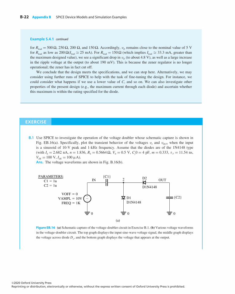
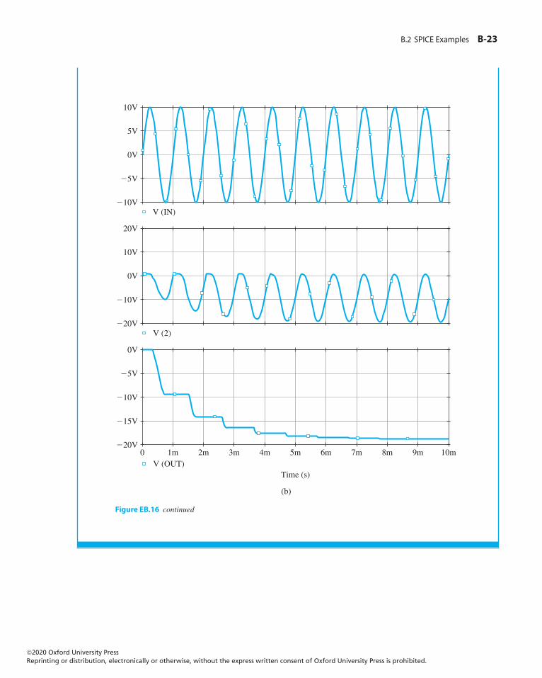
B.1 Use SPICE to investigate the operation of the voltage doubler whose schematic capture is shown inFig. EB.16(a). Specifically, plot the transient behavior of the voltages v2 and vOUT when the inputis a sinusoid of 10-V peak and 1-kHz frequency. Assume that the diodes are of the 1N4148 type(with IS = 2.682 nA, n = 1.836, RS = 0.5664�, V0 = 0.5 V, Cj0 = 4 pF, m = 0.333, τ T = 11.54 ns,VZK = 100 V, IZK = 100 µA).Ans. The voltage waveforms are shown in Fig. B.16(b).
(a)
{C2}
{C1}
D1D1N4148
0 0
2 D2
D1N4148
OUTIN
0
�
�
VOFF � 0VAMPL � 10V FREQ � 1K
PARAMETERS: C1 � 1u C2 � 1u
Figure EB.16 (a) Schematic capture of the voltage-doubler circuit in Exercise B.1. (b)Various voltage waveforms
in the voltage-doubler circuit. The top graph displays the input sine-wave voltage signal, the middle graph displays
the voltage across diode D1, and the bottom graph displays the voltage that appears at the output.
©20 Oxford University PressReprinting or distribution, electronically or otherwise, without the express written consent of Oxford University Press is prohibited.
20
B.2 SPICE Examples B-23
(b)
Time (s)
0 1m 2m 3m 4m 5m 6m 7m 8m 9m 10m�20V
�15V
�10V
�5V
0V
V (IN)�10V
�5V
0V
5V
10V
�20V
�10V
0V
10V
20V
V (2)
V (OUT)
Figure EB.16 continued
©20 Oxford University PressReprinting or distribution, electronically or otherwise, without the express written consent of Oxford University Press is prohibited.
20
B-24 Appendix B SPICE Device Models and Simulation Examples
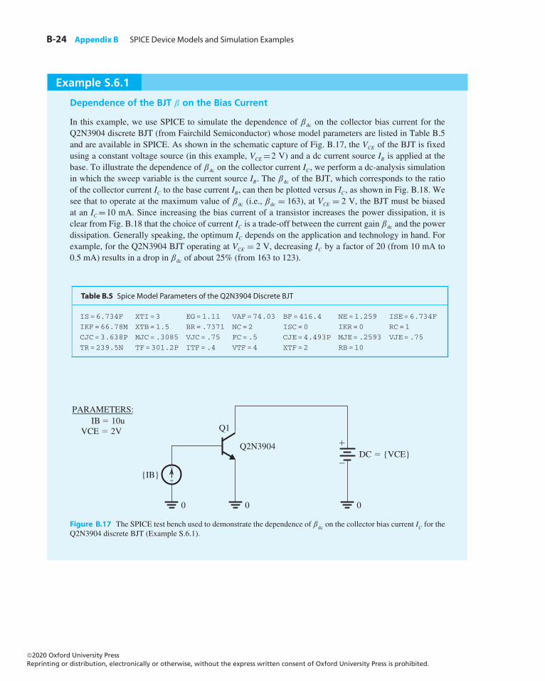
Example S.6.1
Dependence of the BJT β on the Bias Current
In this example, we use SPICE to simulate the dependence of βdc on the collector bias current for theQ2N3904 discrete BJT (from Fairchild Semiconductor) whose model parameters are listed in Table B.5and are available in SPICE. As shown in the schematic capture of Fig. B.17, the VCE of the BJT is fixedusing a constant voltage source (in this example, VCE =2 V) and a dc current source IB is applied at thebase. To illustrate the dependence of βdc on the collector current IC, we perform a dc-analysis simulationin which the sweep variable is the current source IB. The βdc of the BJT, which corresponds to the ratioof the collector current IC to the base current IB, can then be plotted versus IC, as shown in Fig. B.18. Wesee that to operate at the maximum value of βdc (i.e., βdc = 163), at VCE = 2 V, the BJT must be biasedat an IC =10 mA. Since increasing the bias current of a transistor increases the power dissipation, it isclear from Fig. B.18 that the choice of current IC is a trade-off between the current gain βdc and the powerdissipation. Generally speaking, the optimum IC depends on the application and technology in hand. Forexample, for the Q2N3904 BJT operating at VCE = 2 V, decreasing IC by a factor of 20 (from 10 mA to0.5 mA) results in a drop in βdc of about 25% (from 163 to 123).
Table B.5 Spice Model Parameters of the Q2N3904 Discrete BJT
IS=6.734F XTI=3 EG=1.11 VAF=74.03 BF=416.4 NE=1.259 ISE=6.734F
IKF=66.78M XTB=1.5 BR=.7371 NC=2 ISC=0 IKR=0 RC=1
CJC=3.638P MJC=.3085 VJC=.75 FC=.5 CJE=4.493P MJE=.2593 VJE=.75
TR=239.5N TF=301.2P ITF=.4 VTF=4 XTF=2 RB=10
{IB}
IB � 10uVCE � 2V Q1
�
�
DC � {VCE}�
�
000
Q2N3904
PARAMETERS:
Figure B.17 The SPICE test bench used to demonstrate the dependence of βdc on the collector bias current IC for theQ2N3904 discrete BJT (Example S.6.1).
©20 Oxford University PressReprinting or distribution, electronically or otherwise, without the express written consent of Oxford University Press is prohibited.
20
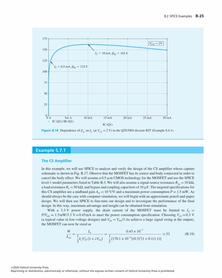
B.2 SPICE Examples B-25
IC (Q1)
0 A 5m A 10 mA 15 mA 20 mA 25 mA 30 mAIC (Q1)�IB (Q1)
0
25
50
75
100
125
150
175
IC � 0.5 mA, bdc � 122.9
IC � 10 mA, bdc � 162.4
VCE � 2V
Figure B.18 Dependence of βdc on IC (at VCE = 2 V) in the Q2N3904 discrete BJT (Example S.6.1).
Example S.7.1
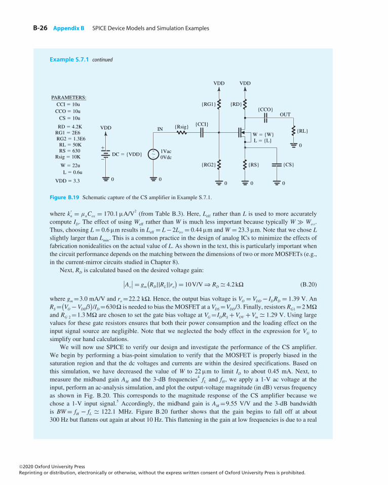
The CS Amplifier
In this example, we will use SPICE to analyze and verify the design of the CS amplifier whose captureschematic is shown in Fig. B.17. Observe that the MOSFET has its source and body connected in order tocancel the body effect. We will assume a 0.5-µm CMOS technology for the MOSFET and use the SPICElevel-1 model parameters listed in Table B.3. We will also assume a signal-source resistance Rsig = 10 k�,a load resistance RL = 50 k�, and bypass and coupling capacitors of 10µF. The targeted specifications forthis CS amplifier are a midband gain AM = 10 V/V and a maximum power consumption P= 1.5 mW. Asshould always be the case with computer simulation, we will begin with an approximate pencil-and-paperdesign. We will then use SPICE to fine-tune our design and to investigate the performance of the finaldesign. In this way, maximum advantage and insight can be obtained from simulation.
With a 3.3-V power supply, the drain current of the MOSFET must be limited to ID =P/VDD = 1.5mW/3.3 V=0.45mA to meet the power consumption specification. Choosing VOV =0.3 V(a typical value in low-voltage designs) and VDS = VDD/3 (to achieve a large signal swing at the output),the MOSFET can now be sized as
W
Leff
= ID1
2k ′nV
2OV
(1+λVDS
) = 0.45× 10⁻³
1
2
(170.1× 10⁻⁶
)(0.3)2[1+ 0.1(1.1)]
� 53 (B.19)
©20 Oxford University PressReprinting or distribution, electronically or otherwise, without the express written consent of Oxford University Press is prohibited.
20
B-26 Appendix B SPICE Device Models and Simulation Examples
Example S.7.1 continued
PARAMETERS: CCI � 10u CCO � 10u CS � 10u
RD � 4.2K RG1 � 2E6 RG2 � 1.3E6 RL � 50K RS � 630 Rsig � 10K
W � 22u L � 0.6u
VDD � 3.3
IN
OUT
W � {W} L � {L}
0
{CCO}{RD}
VDD
{RL}
{RG1}
{Rsig}
VDD
{CS}
00
{RS}
0
{RG2}
{CCI}
1Vac0Vdc
0
�
�
VDD
DC � {VDD}�
�
0
Figure B.19 Schematic capture of the CS amplifier in Example S.7.1.
where k ′n = μnCox = 170.1µA/V2 (from Table B.3). Here, Leff rather than L is used to more accurately
compute ID. The effect of using Weff rather than W is much less important because typically W � Wov.Thus, choosing L= 0.6µm results in Leff = L− 2Lov = 0.44µm and W = 23.3µm. Note that we chose Lslightly larger than Lmin. This is a common practice in the design of analog ICs to minimize the effects offabrication nonidealities on the actual value of L. As shown in the text, this is particularly important whenthe circuit performance depends on the matching between the dimensions of two or more MOSFETs (e.g.,in the current-mirror circuits studied in Chapter 8).
Next, RD is calculated based on the desired voltage gain:∣∣Av
∣∣ = gm(RD||RL||ro
) = 10V/V⇒ RD � 4.2k� (B.20)
where gm=3.0 mA/V and ro=22.2 k�. Hence, the output bias voltage is VO = VDD − IDRD = 1.39 V. AnRS=
(VO −VDD/3
)/ID=630� is needed to bias the MOSFET at a VDS=VDD/3. Finally, resistors RG1 =2M�
and RG 2 =1.3M� are chosen to set the gate bias voltage at VG= IDRS +VOV +Vtn � 1.29 V. Using largevalues for these gate resistors ensures that both their power consumption and the loading effect on theinput signal source are negligible. Note that we neglected the body effect in the expression for VG tosimplify our hand calculations.
We will now use SPICE to verify our design and investigate the performance of the CS amplifier.We begin by performing a bias-point simulation to verify that the MOSFET is properly biased in thesaturation region and that the dc voltages and currents are within the desired specifications. Based onthis simulation, we have decreased the value of W to 22µm to limit ID to about 0.45 mA. Next, tomeasure the midband gain AM and the 3-dB frequencies4 fL and fH , we apply a 1-V ac voltage at theinput, perform an ac-analysis simulation, and plot the output-voltage magnitude (in dB) versus frequencyas shown in Fig. B.20. This corresponds to the magnitude response of the CS amplifier because wechose a 1-V input signal.5 Accordingly, the midband gain is AM =9.55 V/V and the 3-dB bandwidthis BW= fH − fL � 122.1 MHz. Figure B.20 further shows that the gain begins to fall off at about300 Hz but flattens out again at about 10 Hz. This flattening in the gain at low frequencies is due to a real
©20 Oxford University PressReprinting or distribution, electronically or otherwise, without the express written consent of Oxford University Press is prohibited.
20
B.2 SPICE Examples B-27
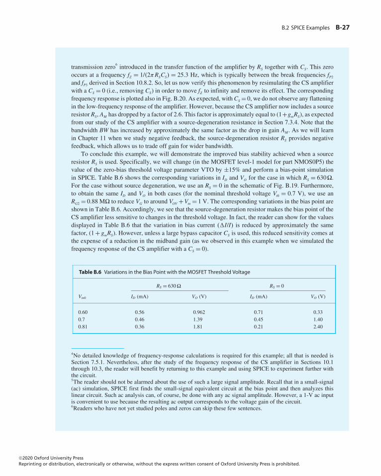
transmission zero6 introduced in the transfer function of the amplifier by RS together with CS. This zerooccurs at a frequency fZ = 1/(2πRSCS) = 25.3 Hz, which is typically between the break frequencies fP2and fP3 derived in Section 10.8.2. So, let us now verify this phenomenon by resimulating the CS amplifierwith a CS = 0 (i.e., removing CS) in order to move fZ to infinity and remove its effect. The correspondingfrequency response is plotted also in Fig. B.20. As expected, withCS = 0, we do not observe any flatteningin the low-frequency response of the amplifier. However, because the CS amplifier now includes a sourceresistor RS, AM has dropped by a factor of 2.6. This factor is approximately equal to (1+gmRS), as expectedfrom our study of the CS amplifier with a source-degeneration resistance in Section 7.3.4. Note that thebandwidth BW has increased by approximately the same factor as the drop in gain AM . As we will learnin Chapter 11 when we study negative feedback, the source-degeneration resistor RS provides negativefeedback, which allows us to trade off gain for wider bandwidth.
To conclude this example, we will demonstrate the improved bias stability achieved when a sourceresistor RS is used. Specifically, we will change (in the MOSFET level-1 model for part NMOS0P5) thevalue of the zero-bias threshold voltage parameter VTO by ±15% and perform a bias-point simulationin SPICE. Table B.6 shows the corresponding variations in ID and VO for the case in which RS = 630�.For the case without source degeneration, we use an RS = 0 in the schematic of Fig. B.19. Furthermore,to obtain the same ID and VO in both cases (for the nominal threshold voltage Vt0 = 0.7 V), we use anRG2 = 0.88 M� to reduce VG to around VOV +Vtn = 1 V. The corresponding variations in the bias point areshown in Table B.6. Accordingly, we see that the source-degeneration resistor makes the bias point of theCS amplifier less sensitive to changes in the threshold voltage. In fact, the reader can show for the valuesdisplayed in Table B.6 that the variation in bias current (I/I) is reduced by approximately the samefactor, (1+ gmRS). However, unless a large bypass capacitor CS is used, this reduced sensitivity comes atthe expense of a reduction in the midband gain (as we observed in this example when we simulated thefrequency response of the CS amplifier with a CS = 0).
Table B.6 Variations in the Bias Point with the MOSFET Threshold Voltage
RS = 630� RS = 0
Vtn0 ID (mA) VO (V) ID (mA) VO (V)
0.60 0.56 0.962 0.71 0.330.7 0.46 1.39 0.45 1.400.81 0.36 1.81 0.21 2.40
4No detailed knowledge of frequency-response calculations is required for this example; all that is needed isSection 7.5.1. Nevertheless, after the study of the frequency response of the CS amplifier in Sections 10.1through 10.3, the reader will benefit by returning to this example and using SPICE to experiment further withthe circuit.5The reader should not be alarmed about the use of such a large signal amplitude. Recall that in a small-signal(ac) simulation, SPICE first finds the small-signal equivalent circuit at the bias point and then analyzes thislinear circuit. Such ac analysis can, of course, be done with any ac signal amplitude. However, a 1-V ac inputis convenient to use because the resulting ac output corresponds to the voltage gain of the circuit.6Readers who have not yet studied poles and zeros can skip these few sentences.
©20 Oxford University PressReprinting or distribution, electronically or otherwise, without the express written consent of Oxford University Press is prohibited.
20
B-28 Appendix B SPICE Device Models and Simulation Examples
Example S.7.1 continued
Frequency (Hz)
100m 1.0 10m 100 1.0K 10 100K 1.0M 10K 100M 1.0G 10M
20
15
10
5
0
dB (V(OUT))
CS � 10 uF
CS � 0
AM � 19.6 dB
AM � 11.3 dB
fH � 122.1 MHz fL � 54.2 Hz
fL � 0.3 Hz fH � 276.5 MHz
Figure B.20 Frequency response of the CS amplifier in Example S.7.1 with CS = 10µF and CS = 0 (i.e., CS
removed).
Example S.7.2
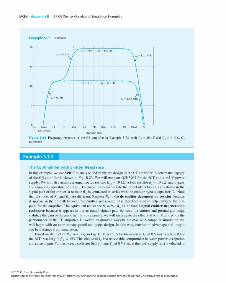
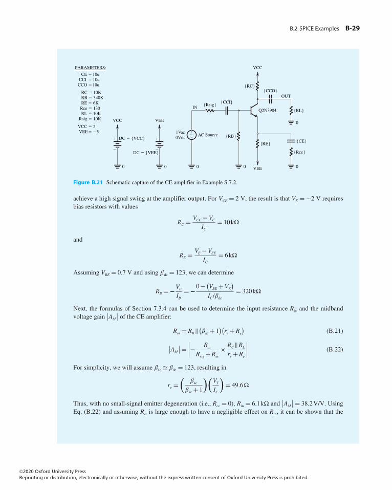
The CE Amplifier with Emitter ResistanceIn this example, we use SPICE to analyze and verify the design of the CE amplifier. A schematic captureof the CE amplifier is shown in Fig. B.23. We will use part Q2N3904 for the BJT and a ±5-V powersupply. We will also assume a signal source resistor Rsig = 10 k�, a load resistor RL = 10 k�, and bypassand coupling capacitors of 10 µF. To enable us to investigate the effect of including a resistance in thesignal path of the emitter, a resistor Rce is connected in series with the emitter bypass capacitor CE. Notethat the roles of RE and Rce are different. Resistor RE is the dc emitter-degeneration resistor becauseit appears in the dc path between the emitter and ground. It is therefore used to help stabilize the biaspoint for the amplifier. The equivalent resistance Re = RE‖Rce is the small-signal emitter-degenerationresistance because it appears in the ac (small-signal) path between the emitter and ground and helpsstabilize the gain of the amplifier. In this example, we will investigate the effects of both RE and Re on theperformance of the CE amplifier. However, as should always be the case with computer simulation, wewill begin with an approximate pencil-and-paper design. In this way, maximum advantage and insightcan be obtained from simulation.
Based on the plot of βdc versus IC in Fig. B.20, a collector bias current IC of 0.5 mA is selected forthe BJT, resulting in βdc = 123. This choice of IC is a reasonable compromise between power dissipationand current gain. Furthermore, a collector bias voltage VC of 0 V (i.e., at the mid–supply rail) is selected to
©20 Oxford University PressReprinting or distribution, electronically or otherwise, without the express written consent of Oxford University Press is prohibited.
20
B.2 SPICE Examples B-29
IN
VCC
Q2N3904
OUT
DC � {VCC}�
�
0
VEE
DC � {VEE}
�
�
0
0
{CCO}{RC}
VCC
VEE
{RL}
{Rce}
{Rsig}
{CE}
0
{RE}
0
{RB}
{CCI}
AC Source1Vac0Vdc
0
�
�
CE � 10u CCI � 10uCCO � 10u
RC � 10K RB � 340K RE � 6K Rce � 130 RL � 10K Rsig � 10K
VCC � 5 VEE � �5
PARAMETERS:
Figure B.21 Schematic capture of the CE amplifier in Example S.7.2.
achieve a high signal swing at the amplifier output. For VCE = 2 V, the result is that VE = −2 V requiresbias resistors with values
RC = VCC −VCIC
= 10k�
and
RE = VE −VEEIC
= 6k�
Assuming VBE = 0.7 V and using βdc = 123, we can determine
RB = −VBIB
= −0− (VBE +VE
)IC/βdc
= 320k�
Next, the formulas of Section 7.3.4 can be used to determine the input resistance Rin and the midbandvoltage gain
∣∣AM
∣∣ of the CE amplifier:
Rin = RB‖(βac + 1
)(re +Re
)(B.21)
∣∣AM
∣∣ =∣∣∣∣− Rin
Rsig +Rin
× RC‖RL
re +Re
∣∣∣∣ (B.22)
For simplicity, we will assume βac � βdc = 123, resulting in
re =(
βac
βac + 1
)(VTIC
)= 49.6�
Thus, with no small-signal emitter degeneration (i.e., Rce = 0), Rin = 6.1k� and∣∣AM
∣∣ = 38.2V/V. UsingEq. (B.22) and assuming RB is large enough to have a negligible effect on Rin, it can be shown that the
©20 Oxford University PressReprinting or distribution, electronically or otherwise, without the express written consent of Oxford University Press is prohibited.
20
B-30 Appendix B SPICE Device Models and Simulation Examples
Example S.7.2 continued
emitter-degeneration resistor Re decreases the voltage gain∣∣AM
∣∣ by a factor of
1+ Re
re+ Rsig
rπ
1+ Rsig
rπTherefore, to limit the reduction in voltage gain to a factor of 2, we will select
Re = re +Rsig
βac + 1(B.23)
Thus, Rce � Re = 130�. Substituting this value in Eqs. (B.21) and (B.22) shows that Rin increases from6.1k� to 20.9k� while
∣∣AM
∣∣ drops from 38.2 V/V to 18.8 V/V.We will now use SPICE to verify our design and investigate the performance of the CE amplifier. We
begin by performing a bias-point simulation to verify that the BJT is properly biased in the active regionand that the dc voltages and currents are within the desired specifications. Based on this simulation, wehave increased the value of RB to 340k� in order to limit IC to about 0.5 mA while using a standard 1%resistor value. Next, to measure the midband gain AM and the 3-dB frequencies9 fL and fH , we apply a 1-Vac voltage at the input, perform an ac-analysis simulation, and plot the output-voltage magnitude (in dB)versus frequency as shown in Fig. B.22. This corresponds to the magnitude response of the CE amplifierbecause we chose a 1-V input signal.10 Accordingly, with no emitter degeneration, the midband gain is∣∣AM
∣∣ = 38.5 V/V = 31.7 dB and the 3-dB bandwidth is BW = fH − fL = 145.7 kHz. Using an Rce of130�
results in a drop in the midband gain∣∣AM
∣∣ by a factor of 2 (i.e., 6 dB). Interestingly, however, BW has nowincreased by approximately the same factor as the drop in
∣∣AM
∣∣. As we learned in Chapter 11 in our studyof negative feedback, the emitter-degeneration resistor Rce provides negative feedback, which allows usto trade off gain for other desirable properties, such as a larger input resistance and a wider bandwidth.
To conclude this example, we will demonstrate the improved bias-point (or dc operating-point)stability achieved when an emitter resistor RE is used. Specifically, we will increase/decrease the value ofthe parameter BF (i.e., the ideal maximum forward current gain) in the SPICE model for part Q2N3904by a factor of 2 and perform a bias-point simulation. The corresponding change in BJT parameters (βdc
and βac) and bias-point (including IC and CE) are presented in Table B.7 for the case of RE = 6k�. Notethat βac is not equal to βdc as we assumed, but is slightly larger. For the case without emitter degeneration,we will use RE = 0 in the schematic of Fig. B.21. Furthermore, to maintain the same IC and VC in bothcases at the values obtained for nominal BF, we use RB = 1.12 M� to limit IC to approximately 0.5 mA.The corresponding variations in the BJT bias point are also shown in Table B.7. Accordingly, we seethat emitter degeneration makes the bias point of the CE amplifier much less sensitive to changes in β.However, unless a large bypass capacitor CE is used, this reduced bias sensitivity comes at the expenseof a reduction in the midband gain (as we observed in this example when we simulated the frequencyresponse of the CE amplifier with an Re = 130�).
9No detailed knowledge of frequency-response calculations is required for this example; all that is needed isSection 7.4.2. Nevertheless, after the study of the frequency response of the CE amplifier in Sections 10.2 and10.8, the reader will benefit by returning to this example to experiment further with the circuit using SPICE.10The reader should not be alarmed about the use of such a large signal amplitude. Recall that in a small-signal(ac) simulation, SPICE first finds the small-signal equivalent circuit at the dc bias point and then analyzes thislinear circuit. Such ac analysis can, of course, be done with any ac signal amplitude. However, a 1-V ac inputis convenient to use because the resulting ac output corresponds to the voltage gain of the circuit.
©20 Oxford University PressReprinting or distribution, electronically or otherwise, without the express written consent of Oxford University Press is prohibited.
20
B.2 SPICE Examples B-31
Frequency (Hz)
1.0 10 100 1.0 K 10 K 100 K 1.0 M 10 M 0
5
10
15
20
25
30
35
dB (V(OUT))
fL � 131.1 Hz AM � 31.7 dB
Rce � 0 �
fH � 287.1 kHz
Rce � 130 �
AM � 25.6 dB
fH � 145.8 kHz
fL � 62.9 Hz
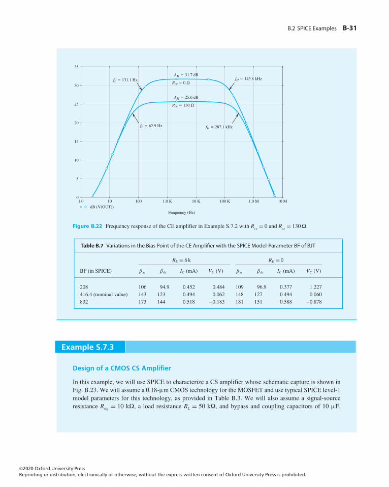
Figure B.22 Frequency response of the CE amplifier in Example S.7.2 with Rce = 0 and Rce = 130�.
Table B.7 Variations in the Bias Point of the CE Amplifier with the SPICE Model-Parameter BF of BJT
RE = 6 k RE = 0
BF (in SPICE) βac βdc IC (mA) VC (V) βac βdc IC (mA) VC (V)
208 106 94.9 0.452 0.484 109 96.9 0.377 1.227416.4 (nominal value) 143 123 0.494 0.062 148 127 0.494 0.060832 173 144 0.518 −0.183 181 151 0.588 −0.878
Example S.7.3
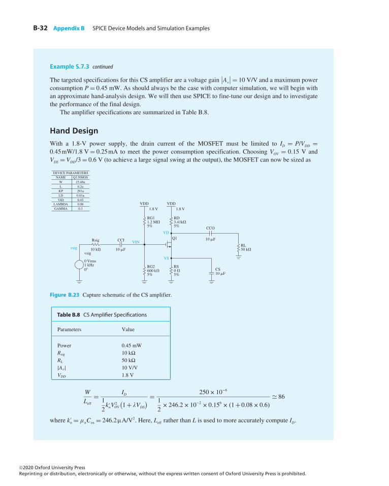
Design of a CMOS CS Amplifier
In this example, we will use SPICE to characterize a CS amplifier whose schematic capture is shown inFig. B.23. We will assume a 0.18-µm CMOS technology for the MOSFET and use typical SPICE level-1model parameters for this technology, as provided in Table B.3. We will also assume a signal-sourceresistance Rsig = 10 k�, a load resistance RL = 50 k�, and bypass and coupling capacitors of 10 µF.
©20 Oxford University PressReprinting or distribution, electronically or otherwise, without the express written consent of Oxford University Press is prohibited.
20
B-32 Appendix B SPICE Device Models and Simulation Examples
Example S.7.3 continued
The targeted specifications for this CS amplifier are a voltage gain∣∣Av
∣∣ = 10 V/V and a maximum powerconsumption P= 0.45 mW. As should always be the case with computer simulation, we will begin withan approximate hand-analysis design. We will then use SPICE to fine-tune our design and to investigatethe performance of the final design.
The amplifier specifications are summarized in Table B.8.
Hand Design
With a 1.8-V power supply, the drain current of the MOSFET must be limited to ID = P/VDD =0.45mW/1.8 V= 0.25mA to meet the power consumption specification. Choosing VOV = 0.15 V andVDS = VDD/3= 0.6 V (to achieve a large signal swing at the output), the MOSFET can now be sized as
10 k� 10 �F
Rsig
vsig vsig
0 Vrms RG2 600 k� 5%
RS 0 � CS
10 �F 5%
RG1
1.8 V 1.8 V VDD
DEVICE PARAMETERS NAME
W L
KP LD VID
LAMBDA GAMMA
Q1:NMOS 15.48u
0.2u 291u 0.01u 0.45 0.08 0.3
VDD
1.2 M� 5%
RD 3.41k� 5%
RL 50 k�
VD
VS
Q1 10 �F
CCO
1 kHz 0�
CCI VIN
Figure B.23 Capture schematic of the CS amplifier.
Table B.8 CS Amplifier Specifications
Parameters Value
Power 0.45 mWRsig 10 k�RL 50 k�|Av| 10 V/VVDD 1.8 V
W
Leff
= ID1
2k ′nV
2OV
(1+λVDS
) = 250× 10−6
1
2× 246.2× 10−2 × 0.156 × (1+ 0.08× 0.6)
� 86
where k ′n = μnCox = 246.2µA/V2. Here, Leff rather than L is used to more accurately compute ID.
©20 Oxford University PressReprinting or distribution, electronically or otherwise, without the express written consent of Oxford University Press is prohibited.
20
B.2 SPICE Examples B-33
The effect of using Weff instead of W is much less important, because typically W � Wov. Thus,choosing L= 0.200µm results in Leff = L− 2Lov = 0.180µm, and W = 86×Leff = 15.48µm.
Note that we chose L slightly larger than Lmin. This is a common practice in the design of analogICs to minimize the effects of fabrication nonidealities on the actual value of L. As we have seen, this isparticularly important when the circuit performance depends on the matching between the dimensions oftwo or more MOSFETs (e.g., in the current-mirror circuits studied in Chapter 8).
Next, RD is calculated based on the desired voltage gain:∣∣Av
∣∣ = gm(RD‖RL‖ro
) = 10V/V⇒ RD � 3.41 k�
where
gm = 2IDVOV
= 2× 0.25× 10−3
0.15= 3.33mA/V
and
ro = VAID
= 12.5
0.25× 10−3 = 50k�
Hence, the dc bias voltage is VD = VDD − IDRD = 0.9457V.To stabilize the bias point of the CS amplifier, we include a resistor in the source lead. In other words,
to bias the MOSFET at VDS = VDD/3, we need an
Rs =VSID
=(VD −VDD/3
)ID
= 0.3475
0.25× 10−3 = 1.39 k�
However, as a result of including such a resistor, the gain drops by a factor of (1+ gmRS). Therefore, weinclude a capacitor, CS, to eliminate the effect of RS on ac operation of the amplifier and gain.
Finally, choosing the current in the biasing branch to be 1µA gives RG1 +RG2 = VDD/1µA= 1.8�.Also, we know that
VGS = VOV +Vt = 0.15+ 0.45= 0.6V⇒ VG = VS + 0.6= 0.3475+ 0.6= 0.9475V
Hence,RG2
RG1 +RG2
= VGVDD
= 0.9475
1.8⇒ RG1 = 0.8525M�,RG2 = 0.9475 M�
Using large values for these gate resistors ensures that both their power consumption and the loadingeffect on the input signal source are negligible.
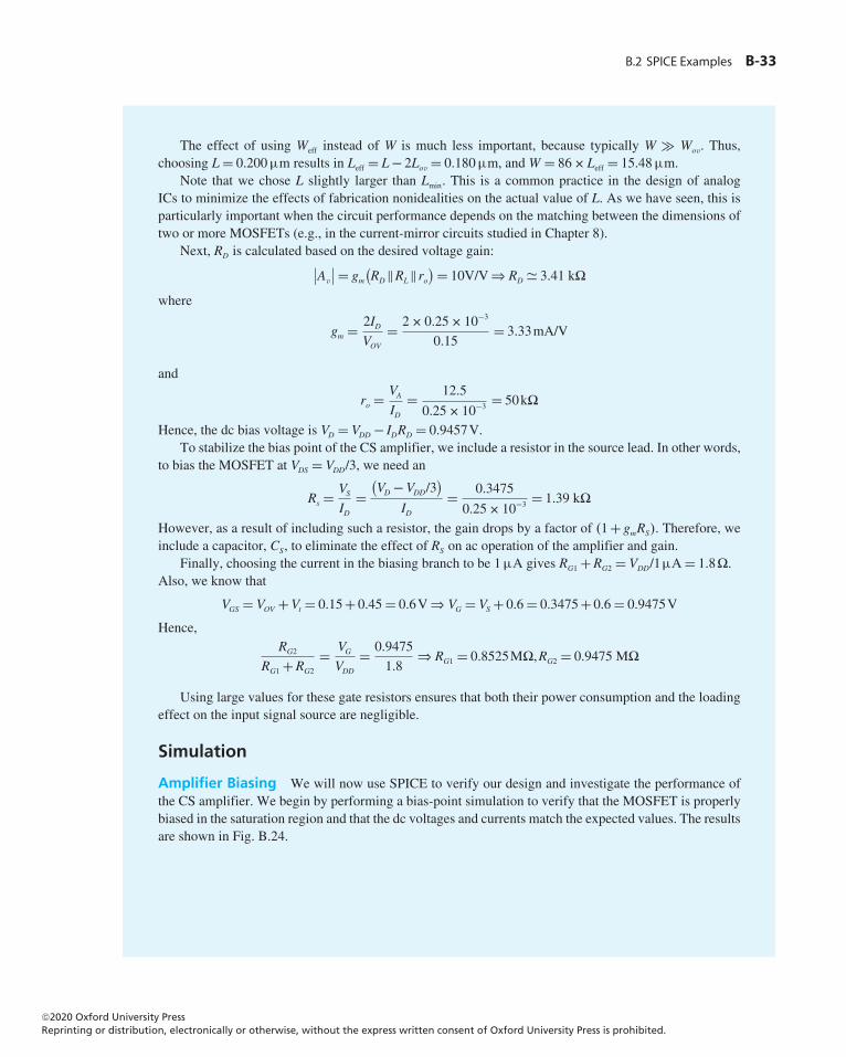
Simulation
Amplifier Biasing We will now use SPICE to verify our design and investigate the performance ofthe CS amplifier. We begin by performing a bias-point simulation to verify that the MOSFET is properlybiased in the saturation region and that the dc voltages and currents match the expected values. The resultsare shown in Fig. B.24.
©20 Oxford University PressReprinting or distribution, electronically or otherwise, without the express written consent of Oxford University Press is prohibited.
20
B-34 Appendix B SPICE Device Models and Simulation Examples
Example S.7.3 continued
VDD
1.8 V
RG1852.5 k�5%
RG2947.5 k�5% RS
1.39 k�5%
RD3.41 k�5%
Q1
VD
VS
1.8 V
V: 948 mVI: 250 uA
V: 347 mVI: 250 uA
V: 947 mVI: 0 A
VDD
Figure B.24 DC bias-point analysis ofthe CS amplifier.
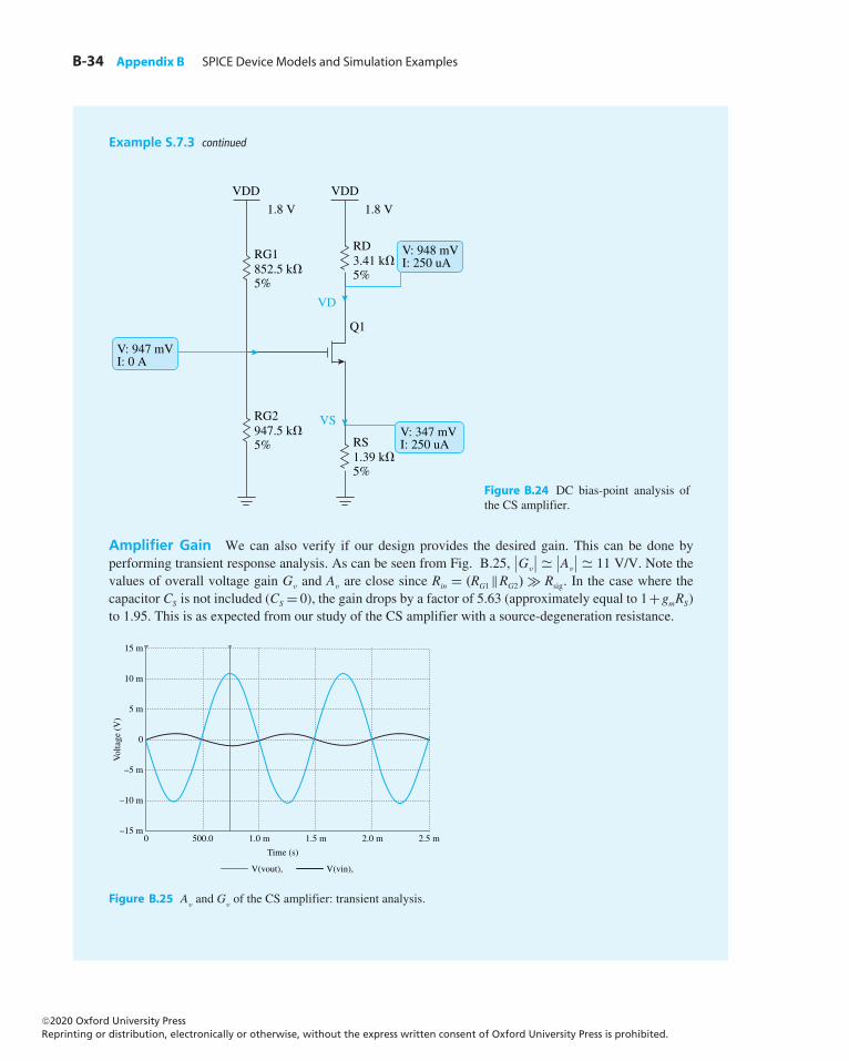
Amplifier Gain We can also verify if our design provides the desired gain. This can be done byperforming transient response analysis. As can be seen from Fig. B.25,
∣∣Gv
∣∣ � ∣∣Av
∣∣ � 11 V/V. Note thevalues of overall voltage gain Gv and Av are close since Rin = (RG1‖RG2) � Rsig. In the case where thecapacitor CS is not included (CS = 0), the gain drops by a factor of 5.63 (approximately equal to 1+gmRS)to 1.95. This is as expected from our study of the CS amplifier with a source-degeneration resistance.
15 m
10 m
5 m
0
Vol
tage
(V
)
–5 m
–10 m
–15 m0 500.0 1.0 m 1.5 m
Time (s)
2.0 m 2.5 m
V(vout), V(vin),
Figure B.25 Av and Gv of the CS amplifier: transient analysis.
©20 Oxford University PressReprinting or distribution, electronically or otherwise, without the express written consent of Oxford University Press is prohibited.
20
B.2 SPICE Examples B-35
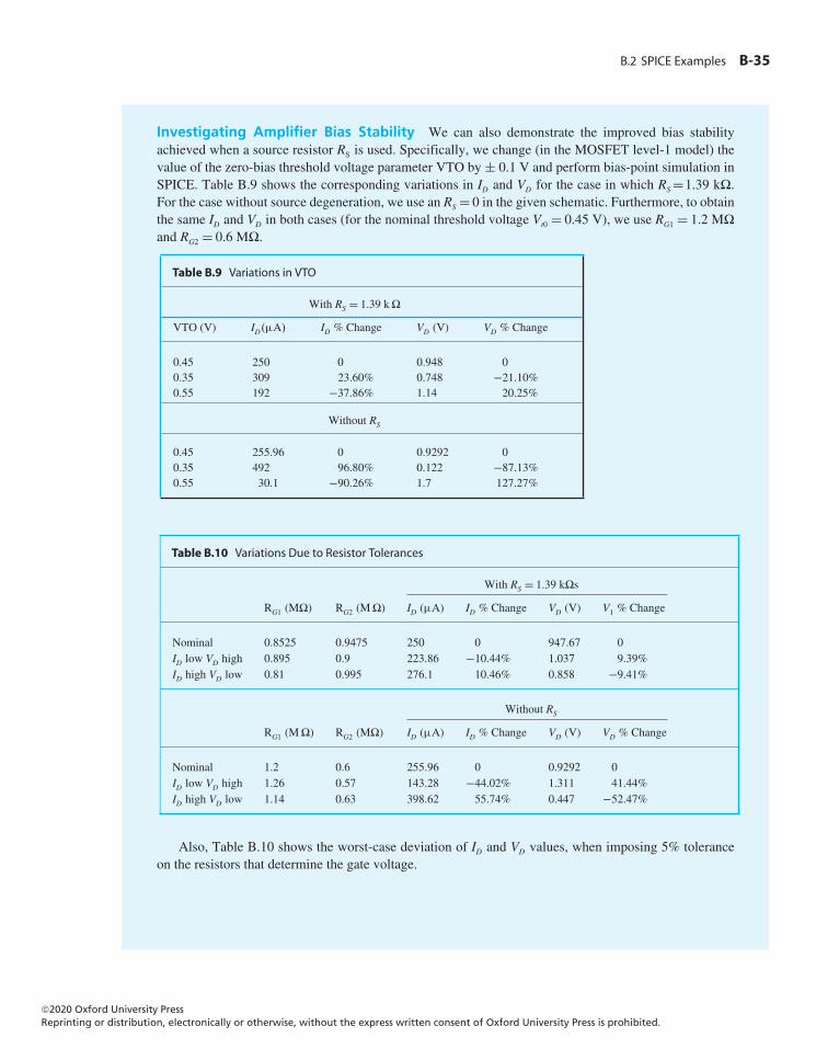
Investigating Amplifier Bias Stability We can also demonstrate the improved bias stabilityachieved when a source resistor RS is used. Specifically, we change (in the MOSFET level-1 model) thevalue of the zero-bias threshold voltage parameter VTO by ± 0.1 V and perform bias-point simulation inSPICE. Table B.9 shows the corresponding variations in ID and VD for the case in which RS=1.39 k�.For the case without source degeneration, we use an RS = 0 in the given schematic. Furthermore, to obtainthe same ID and VD in both cases (for the nominal threshold voltage Vt0 = 0.45 V), we use RG1 = 1.2 M�
and RG2 = 0.6 M�.
Table B.9 Variations in VTO
With RS = 1.39 k�
VTO (V) ID(µA) ID % Change VD (V) VD % Change
0.45 250 0 0.948 00.35 309 23.60% 0.748 −21.10%0.55 192 −37.86% 1.14 20.25%
Without RS
0.45 255.96 0 0.9292 00.35 492 96.80% 0.122 −87.13%0.55 30.1 −90.26% 1.7 127.27%
Table B.10 Variations Due to Resistor Tolerances
With RS = 1.39 k�s
RG1 (M�) RG2 (M�) ID (µA) ID % Change VD (V) V1 % Change
Nominal 0.8525 0.9475 250 0 947.67 0ID low VD high 0.895 0.9 223.86 −10.44% 1.037 9.39%ID high VD low 0.81 0.995 276.1 10.46% 0.858 −9.41%
Without RS
RG1 (M�) RG2 (M�) ID (µA) ID % Change VD (V) VD % Change
Nominal 1.2 0.6 255.96 0 0.9292 0ID low VD high 1.26 0.57 143.28 −44.02% 1.311 41.44%ID high VD low 1.14 0.63 398.62 55.74% 0.447 −52.47%
Also, Table B.10 shows the worst-case deviation of ID and VD values, when imposing 5% toleranceon the resistors that determine the gate voltage.
©20 Oxford University PressReprinting or distribution, electronically or otherwise, without the express written consent of Oxford University Press is prohibited.
20
B-36 Appendix B SPICE Device Models and Simulation Examples
Example S.7.3 continued
Accordingly, we see that the source-degeneration resistor makes the bias point of the CS amplifierless sensitive to changes in the threshold voltage and the values of gate resistors. However, unless a largebypass capacitor CS is used, this reduced sensitivity comes at the expense of a reduction in gain.
Largest Allowable Input Signal Swing Next, we wish to analyze this amplifier circuit todetermine the largest allowable vsig for which the transistor remains in saturation:
vDS ≥ vGS − vt
By enforcing this condition, with equality, at the point vGS is maximum and vDS is correspondinglyminimum, we write:
vDS,min ≥ vGS,max − vt0
vDS −∣∣Gv
∣∣vsig = VGS + vsig − vt0
vsig = VDS −VGS +Vt0(1+ ∣∣Gv
∣∣) = 0.9475− 0.6+ 0.45
11= 72.5mV
If we increase the source signal’s amplitude beyond approximately 73 mV, we can observe the distortionin the output signal, indicating that the MOSFET has entered the triode region.
Amplifier Linearity Finally, we can investigate the linearity of the designed amplifier. In this case,we use a triangular waveform and increase the amplitude of the signal until the output waveform beginsto show nonlinear distortion (i.e., the rising and falling edges are no longer straight lines). Based on handanalysis, linearity holds as long as vin � 2Vov. According to the simulation results, linearity holds until vinreaches the value of approximately 30 mV, which is one-tenth of the value of 2Vov.
Example S.8.1
The CS Amplifier with Active load
In this example, we will use SPICE to compute the dc transfer characteristic of the CS amplifier whosecapture schematic is shown in Fig. B.27. We will assume a 5-µm CMOS technology for the MOSFETsand use parts NMOS5P0 and PMOS5P0 whose SPICE level-1 parameters are listed in Table B.3. Tospecify the dimensions of the MOSFETs in SPICE, we will use the multiplicative factor m together withthe channel length L and the channel width W. The MOSFET parameter m, whose default value is 1, isused in SPICE to specify the number of MOSFETs connected in parallel. As depicted in Fig. B.28, awide transistor with channel length L and channel width m × W can be implemented using m narrowertransistors in parallel, each having a channel length L and a channel width W. Thus, neglecting thechannel-length modulation effect, the drain current of a MOSFET operating in the saturation region canbe expressed as
©20 Oxford University PressReprinting or distribution, electronically or otherwise, without the express written consent of Oxford University Press is prohibited.
20
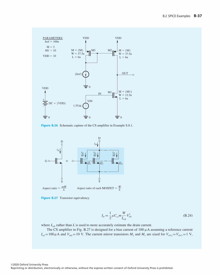
B.2 SPICE Examples B-37
0
PARAMETERS: Iref � 100u
M � 2 M1 � 10
VDD VDD
M � {M}W � 37.5u L � 6u
M � {M}W � 37.5u L � 6u
M � {M1}W � 12.5u L � 6u
VDD
DC � {VDD}�
�
0 0
�
�
�
�
OUT
IN
0
M3 M2
{Iref}
1.5Vdc
VIN
M1
VDD � 10
Figure B.26 Schematic capture of the CS amplifier in Example S.8.1.
iD
D
S
G
Aspect ratio � mWL Aspect ratio of each MOSFET � W
L
iD
Q1 Q2 Qm
D
S
iDm
iDm
iDm
Figure B.27 Transistor equivalency.
ID = 1
2μCoxm
W
Leff
V2OV (B.24)
where Leff rather than L is used to more accurately estimate the drain current.The CS amplifier in Fig. B.27 is designed for a bias current of 100 µA assuming a reference current
Iref =100µA and VDD=10 V. The current mirror transistors M2 and M3 are sized for VOV2 =VOV3 =1 V,
©20 Oxford University PressReprinting or distribution, electronically or otherwise, without the express written consent of Oxford University Press is prohibited.
20
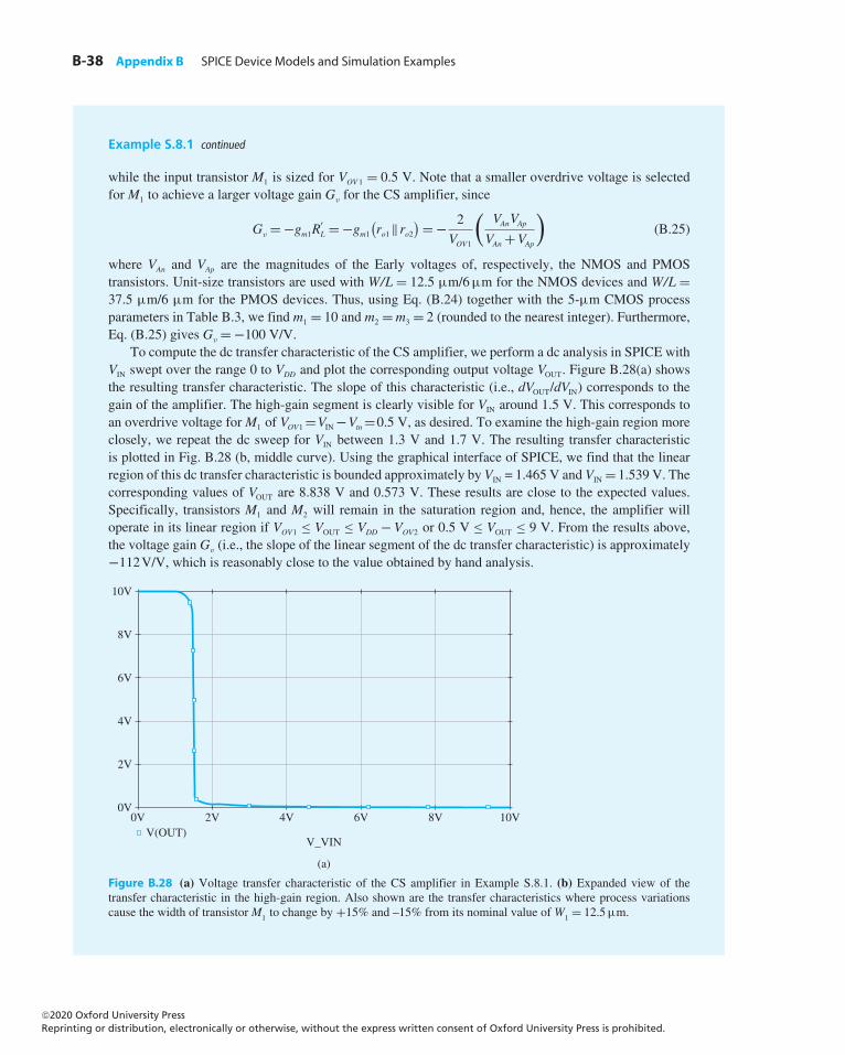
B-38 Appendix B SPICE Device Models and Simulation Examples
Example S.8.1 continued
while the input transistor M1 is sized for VOV 1 = 0.5 V. Note that a smaller overdrive voltage is selectedfor M1 to achieve a larger voltage gain Gv for the CS amplifier, since
Gv = −gm1R′L = −gm1
(ro1‖ro2
) = − 2
VOV1
(VAnVApVAn +VAp
)(B.25)
where VAn and VAp are the magnitudes of the Early voltages of, respectively, the NMOS and PMOStransistors. Unit-size transistors are used with W/L = 12.5 µm/6µm for the NMOS devices and W/L =37.5 µm/6 µm for the PMOS devices. Thus, using Eq. (B.24) together with the 5-µm CMOS processparameters in Table B.3, we find m1 = 10 and m2 =m3 = 2 (rounded to the nearest integer). Furthermore,Eq. (B.25) gives Gv = −100 V/V.
To compute the dc transfer characteristic of the CS amplifier, we perform a dc analysis in SPICE withVIN swept over the range 0 to VDD and plot the corresponding output voltage VOUT. Figure B.28(a) showsthe resulting transfer characteristic. The slope of this characteristic (i.e., dVOUT/dVIN) corresponds to thegain of the amplifier. The high-gain segment is clearly visible for VIN around 1.5 V. This corresponds toan overdrive voltage forM1 of VOV1 =VIN −Vtn=0.5 V, as desired. To examine the high-gain region moreclosely, we repeat the dc sweep for VIN between 1.3 V and 1.7 V. The resulting transfer characteristicis plotted in Fig. B.28 (b, middle curve). Using the graphical interface of SPICE, we find that the linearregion of this dc transfer characteristic is bounded approximately by VIN = 1.465 V and VIN = 1.539 V. Thecorresponding values of VOUT are 8.838 V and 0.573 V. These results are close to the expected values.Specifically, transistors M1 and M2 will remain in the saturation region and, hence, the amplifier willoperate in its linear region if VOV1 ≤ VOUT ≤ VDD −VOV2 or 0.5 V ≤ VOUT ≤ 9 V. From the results above,the voltage gain Gv (i.e., the slope of the linear segment of the dc transfer characteristic) is approximately−112V/V, which is reasonably close to the value obtained by hand analysis.
V_VIN
(a)
0V 2V 4V 6V 8V 10VV(OUT)
0V
2V
4V
6V
8V
10V
Figure B.28 (a) Voltage transfer characteristic of the CS amplifier in Example S.8.1. (b) Expanded view of thetransfer characteristic in the high-gain region. Also shown are the transfer characteristics where process variationscause the width of transistor M1 to change by +15% and –15% from its nominal value of W1 = 12.5µm.
©20 Oxford University PressReprinting or distribution, electronically or otherwise, without the express written consent of Oxford University Press is prohibited.
20
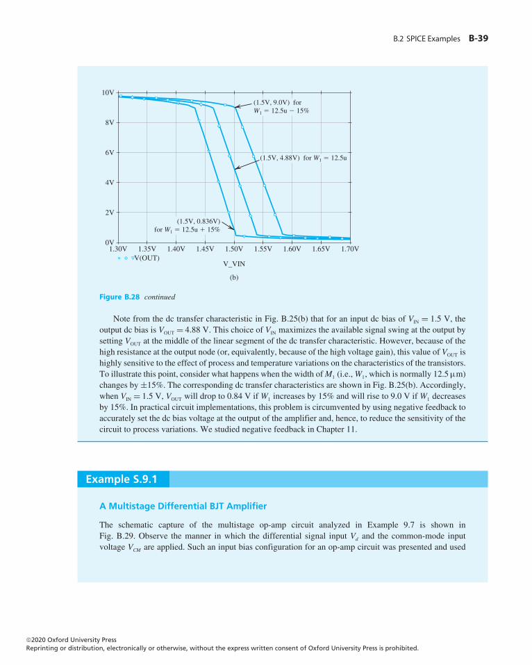
B.2 SPICE Examples B-39
V(OUT)V_VIN
1.30V 1.35V 1.40V 1.45V 1.50V 1.55V 1.60V 1.65V 1.70V0V
2V
4V
6V
8V
10V
(b)
(1.5V, 0.836V)for W1 � 12.5u � 15%
(1.5V, 4.88V) for W1 � 12.5u
(1.5V, 9.0V) forW1 � 12.5u � 15%
Figure B.28 continued
Note from the dc transfer characteristic in Fig. B.25(b) that for an input dc bias of VIN = 1.5 V, theoutput dc bias is VOUT = 4.88 V. This choice of VIN maximizes the available signal swing at the output bysetting VOUT at the middle of the linear segment of the dc transfer characteristic. However, because of thehigh resistance at the output node (or, equivalently, because of the high voltage gain), this value of VOUT ishighly sensitive to the effect of process and temperature variations on the characteristics of the transistors.To illustrate this point, consider what happens when the width ofM1 (i.e.,W1, which is normally 12.5µm)changes by ±15%. The corresponding dc transfer characteristics are shown in Fig. B.25(b). Accordingly,when VIN = 1.5 V, VOUT will drop to 0.84 V if W1 increases by 15% and will rise to 9.0 V ifW1 decreasesby 15%. In practical circuit implementations, this problem is circumvented by using negative feedback toaccurately set the dc bias voltage at the output of the amplifier and, hence, to reduce the sensitivity of thecircuit to process variations. We studied negative feedback in Chapter 11.
Example S.9.1
A Multistage Differential BJT Amplifier
The schematic capture of the multistage op-amp circuit analyzed in Example 9.7 is shown inFig. B.29. Observe the manner in which the differential signal input Vd and the common-mode inputvoltage VCM are applied. Such an input bias configuration for an op-amp circuit was presented and used
©20 Oxford University PressReprinting or distribution, electronically or otherwise, without the express written consent of Oxford University Press is prohibited.
20
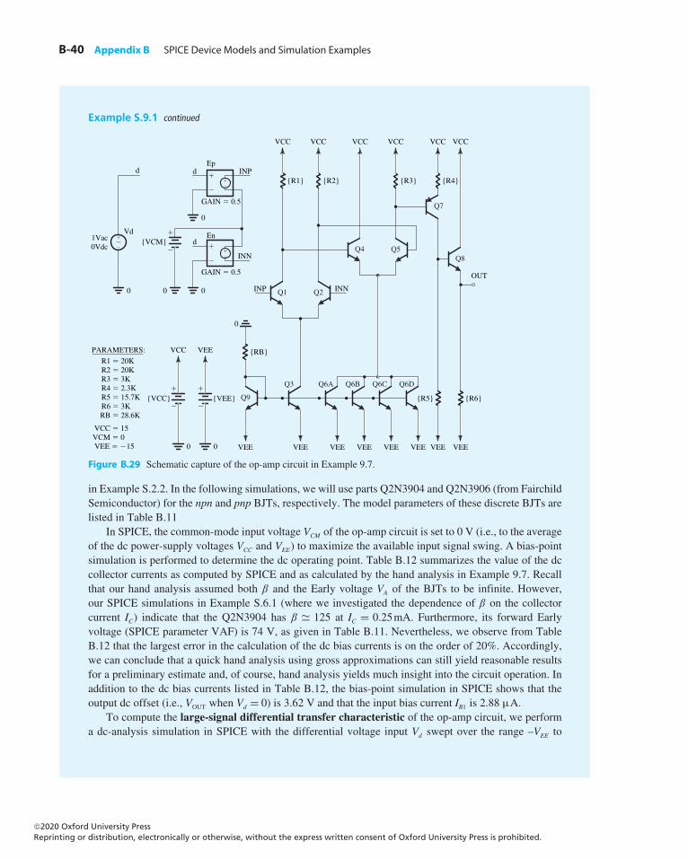
B-40 Appendix B SPICE Device Models and Simulation Examples
Example S.9.1 continued
Q2
INN
INNINP
d{VCM}
{VCC} {VEE}
GAIN � 0.5
0
{RB}R1 � 20K R2 � 20K R3 � 3K R4 � 2.3K R5 � 15.7KR6 � 3K RB � 28.6K
VCC � 15 VCM � 0 VEE � �15
PARAMETERS:
1Vac0Vdc
Vd
0
d
�
�
{R3}
VCC
{R4}
VCC
{R6}
OUT
VEE
VCCVCC
{R2}
VCC
{R1}
VCC
Q5Q4
Q7
Q8
{R5}
VEE
Q1
�
�
0 0
Q6D
VEE
Q6C
VEE
Q6B
VEE
Q6A
VEE
Q3
VEEVEE
Q9
VEE
�
�
0
VCC
�
�
0
�
�
��
En
INPd
GAIN � 0.5
0
�
�
��
Ep
Figure B.29 Schematic capture of the op-amp circuit in Example 9.7.
in Example S.2.2. In the following simulations, we will use parts Q2N3904 and Q2N3906 (from FairchildSemiconductor) for the npn and pnp BJTs, respectively. The model parameters of these discrete BJTs arelisted in Table B.11
In SPICE, the common-mode input voltage VCM of the op-amp circuit is set to 0 V (i.e., to the averageof the dc power-supply voltages VCC and VEE) to maximize the available input signal swing. A bias-pointsimulation is performed to determine the dc operating point. Table B.12 summarizes the value of the dccollector currents as computed by SPICE and as calculated by the hand analysis in Example 9.7. Recallthat our hand analysis assumed both β and the Early voltage VA of the BJTs to be infinite. However,our SPICE simulations in Example S.6.1 (where we investigated the dependence of β on the collectorcurrent IC) indicate that the Q2N3904 has β � 125 at IC = 0.25mA. Furthermore, its forward Earlyvoltage (SPICE parameter VAF) is 74 V, as given in Table B.11. Nevertheless, we observe from TableB.12 that the largest error in the calculation of the dc bias currents is on the order of 20%. Accordingly,we can conclude that a quick hand analysis using gross approximations can still yield reasonable resultsfor a preliminary estimate and, of course, hand analysis yields much insight into the circuit operation. Inaddition to the dc bias currents listed in Table B.12, the bias-point simulation in SPICE shows that theoutput dc offset (i.e., VOUT when Vd = 0) is 3.62 V and that the input bias current IB1 is 2.88 µA.
To compute the large-signal differential transfer characteristic of the op-amp circuit, we performa dc-analysis simulation in SPICE with the differential voltage input Vd swept over the range –VEE to
©20 Oxford University PressReprinting or distribution, electronically or otherwise, without the express written consent of Oxford University Press is prohibited.
20
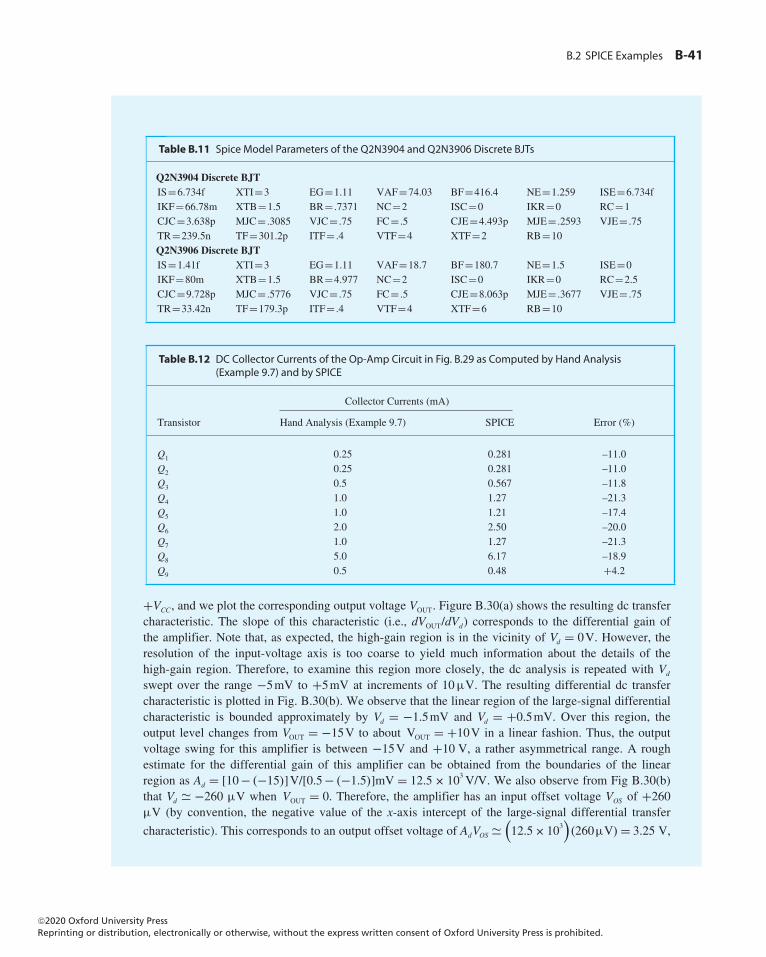
B.2 SPICE Examples B-41
Table B.11 Spice Model Parameters of the Q2N3904 and Q2N3906 Discrete BJTs
Q2N3904 Discrete BJTIS=6.734f XTI=3 EG=1.11 VAF=74.03 BF=416.4 NE=1.259 ISE=6.734fIKF=66.78m XTB=1.5 BR= .7371 NC=2 ISC=0 IKR=0 RC=1CJC=3.638p MJC= .3085 VJC= .75 FC= .5 CJE=4.493p MJE= .2593 VJE= .75TR=239.5n TF=301.2p ITF= .4 VTF=4 XTF=2 RB=10Q2N3906 Discrete BJTIS=1.41f XTI=3 EG=1.11 VAF=18.7 BF=180.7 NE=1.5 ISE=0IKF=80m XTB=1.5 BR=4.977 NC=2 ISC=0 IKR=0 RC=2.5CJC=9.728p MJC= .5776 VJC= .75 FC= .5 CJE=8.063p MJE= .3677 VJE= .75TR=33.42n TF=179.3p ITF= .4 VTF=4 XTF=6 RB=10
Table B.12 DC Collector Currents of the Op-Amp Circuit in Fig. B.29 as Computed by Hand Analysis(Example 9.7) and by SPICE
Collector Currents (mA)
Transistor Hand Analysis (Example 9.7) SPICE Error (%)
Q1 0.25 0.281 –11.0Q2 0.25 0.281 –11.0Q3 0.5 0.567 –11.8Q4 1.0 1.27 –21.3Q5 1.0 1.21 –17.4Q6 2.0 2.50 –20.0Q7 1.0 1.27 –21.3Q8 5.0 6.17 –18.9Q9 0.5 0.48 +4.2
+VCC, and we plot the corresponding output voltage VOUT. Figure B.30(a) shows the resulting dc transfercharacteristic. The slope of this characteristic (i.e., dVOUT/dVd) corresponds to the differential gain ofthe amplifier. Note that, as expected, the high-gain region is in the vicinity of Vd = 0V. However, theresolution of the input-voltage axis is too coarse to yield much information about the details of thehigh-gain region. Therefore, to examine this region more closely, the dc analysis is repeated with Vd
swept over the range −5mV to +5mV at increments of 10µV. The resulting differential dc transfercharacteristic is plotted in Fig. B.30(b). We observe that the linear region of the large-signal differentialcharacteristic is bounded approximately by Vd = −1.5mV and Vd = +0.5mV. Over this region, theoutput level changes from VOUT = −15V to about VOUT = +10V in a linear fashion. Thus, the outputvoltage swing for this amplifier is between −15V and +10 V, a rather asymmetrical range. A roughestimate for the differential gain of this amplifier can be obtained from the boundaries of the linearregion as Ad = [10− (−15)]V/[0.5− (−1.5)]mV = 12.5× 10³V/V. We also observe from Fig B.30(b)that Vd � −260 µV when VOUT = 0. Therefore, the amplifier has an input offset voltage VOS of +260µV (by convention, the negative value of the x-axis intercept of the large-signal differential transfer
characteristic). This corresponds to an output offset voltage of AdVOS �(12.5× 10³
)(260µV) = 3.25 V,
©20 Oxford University PressReprinting or distribution, electronically or otherwise, without the express written consent of Oxford University Press is prohibited.
20
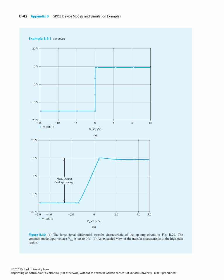
B-42 Appendix B SPICE Device Models and Simulation Examples
Example S.9.1 continued
�10�15 �5 50 10 15
20 V
10 V
0 V
�10 V
�20 V
V_Vd (V)
(a)
V (OUT)
�4.0�5.0 �2.0 2.00 4.0 5.0
20 V
10 V
0 V
�10 V
�20 V
V_Vd (mV)
(b)
V (OUT)
Max. OutputVoltage Swing
Figure B.30 (a) The large-signal differential transfer characteristic of the op-amp circuit in Fig. B.29. Thecommon-mode input voltage VCM is set to 0 V. (b) An expanded view of the transfer characteristic in the high-gainregion.
©20 Oxford University PressReprinting or distribution, electronically or otherwise, without the express written consent of Oxford University Press is prohibited.
20
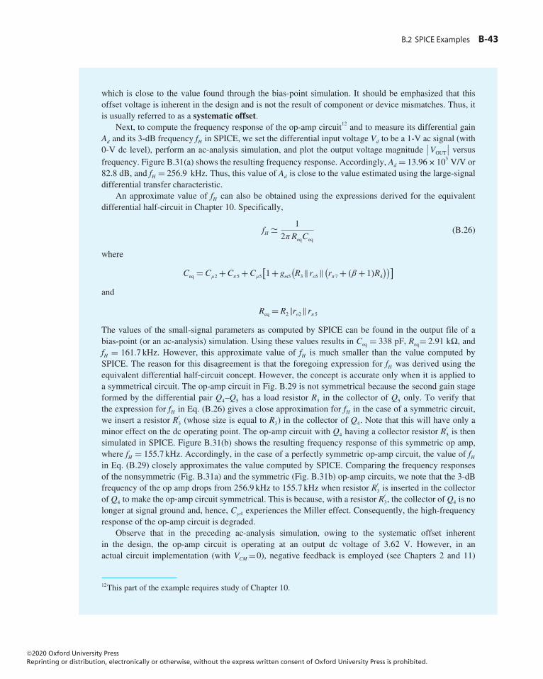
B.2 SPICE Examples B-43
which is close to the value found through the bias-point simulation. It should be emphasized that thisoffset voltage is inherent in the design and is not the result of component or device mismatches. Thus, itis usually referred to as a systematic offset.
Next, to compute the frequency response of the op-amp circuit12 and to measure its differential gainAd and its 3-dB frequency fH in SPICE, we set the differential input voltage Vd to be a 1-V ac signal (with0-V dc level), perform an ac-analysis simulation, and plot the output voltage magnitude
∣∣VOUT
∣∣ versusfrequency. Figure B.31(a) shows the resulting frequency response. Accordingly, Ad = 13.96×10³ V/V or82.8 dB, and fH = 256.9 kHz. Thus, this value of Ad is close to the value estimated using the large-signaldifferential transfer characteristic.
An approximate value of fH can also be obtained using the expressions derived for the equivalentdifferential half-circuit in Chapter 10. Specifically,
fH � 1
2πReqCeq
(B.26)
where
Ceq = Cμ2 +Cπ5 +Cμ5
[1+ gm5
(R3‖ro5‖
(rπ7 + (β + 1)R4
))]and
Req = R2 |ro2‖rπ5The values of the small-signal parameters as computed by SPICE can be found in the output file of abias-point (or an ac-analysis) simulation. Using these values results in Ceq = 338 pF, Req= 2.91 k�, andfH = 161.7 kHz. However, this approximate value of fH is much smaller than the value computed bySPICE. The reason for this disagreement is that the foregoing expression for fH was derived using theequivalent differential half-circuit concept. However, the concept is accurate only when it is applied toa symmetrical circuit. The op-amp circuit in Fig. B.29 is not symmetrical because the second gain stageformed by the differential pair Q4–Q5 has a load resistor R3 in the collector of Q5 only. To verify thatthe expression for fH in Eq. (B.26) gives a close approximation for fH in the case of a symmetric circuit,we insert a resistor R′
3 (whose size is equal to R3) in the collector of Q4. Note that this will have only aminor effect on the dc operating point. The op-amp circuit with Q4 having a collector resistor R′
3 is thensimulated in SPICE. Figure B.31(b) shows the resulting frequency response of this symmetric op amp,where fH = 155.7 kHz. Accordingly, in the case of a perfectly symmetric op-amp circuit, the value of fHin Eq. (B.29) closely approximates the value computed by SPICE. Comparing the frequency responsesof the nonsymmetric (Fig. B.31a) and the symmetric (Fig. B.31b) op-amp circuits, we note that the 3-dBfrequency of the op amp drops from 256.9 kHz to 155.7 kHz when resistor R′
3 is inserted in the collectorof Q4 to make the op-amp circuit symmetrical. This is because, with a resistor R′
3, the collector of Q4 is nolonger at signal ground and, hence, Cμ4 experiences the Miller effect. Consequently, the high-frequencyresponse of the op-amp circuit is degraded.
Observe that in the preceding ac-analysis simulation, owing to the systematic offset inherentin the design, the op-amp circuit is operating at an output dc voltage of 3.62 V. However, in anactual circuit implementation (with VCM =0), negative feedback is employed (see Chapters 2 and 11)
12This part of the example requires study of Chapter 10.
©20 Oxford University PressReprinting or distribution, electronically or otherwise, without the express written consent of Oxford University Press is prohibited.
20
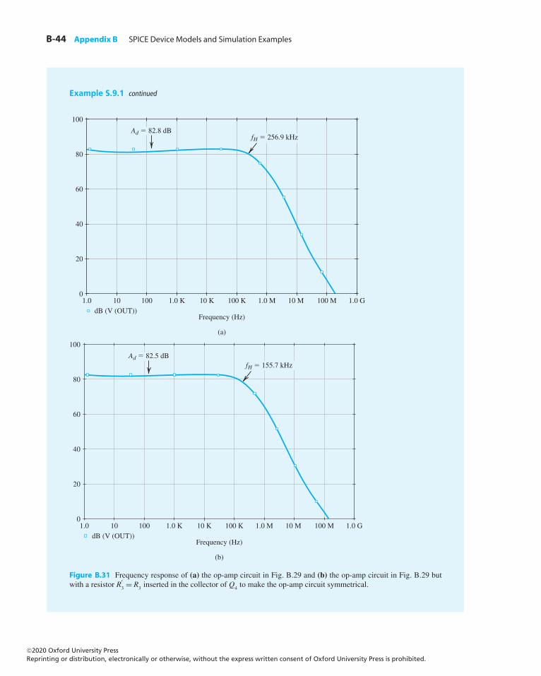
B-44 Appendix B SPICE Device Models and Simulation Examples
Example S.9.1 continued
100
Frequency (Hz)
(a)
1.0dB (V (OUT))
10 100 1.0 K 10 K 100 K 1.0 M 10 M 100 M 1.0 G
Ad � 82.8 dBfH � 256.9 kHz
80
60
40
20
0
100
Frequency (Hz)
(b)
1.0dB (V (OUT))
10 100 1.0 K 10 K 100 K 1.0 M 10 M 100 M 1.0 G
Ad � 82.5 dBfH � 155.7 kHz
80
60
40
20
0
Figure B.31 Frequency response of (a) the op-amp circuit in Fig. B.29 and (b) the op-amp circuit in Fig. B.29 butwith a resistor R
′3 = R3 inserted in the collector of Q4 to make the op-amp circuit symmetrical.
©20 Oxford University PressReprinting or distribution, electronically or otherwise, without the express written consent of Oxford University Press is prohibited.
20
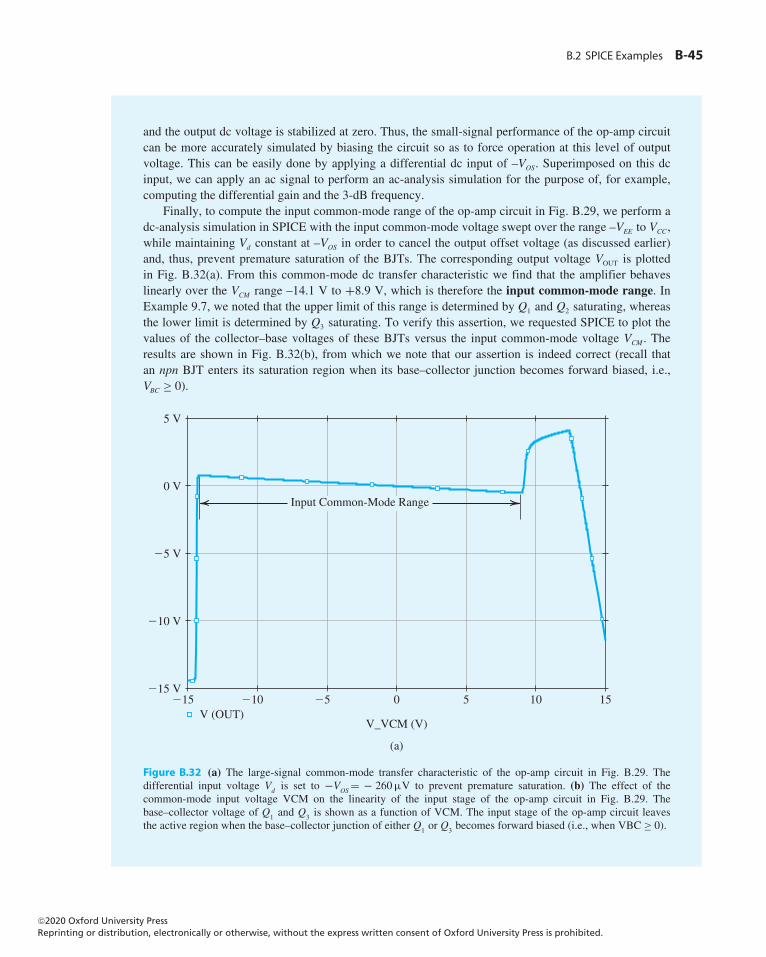
B.2 SPICE Examples B-45
and the output dc voltage is stabilized at zero. Thus, the small-signal performance of the op-amp circuitcan be more accurately simulated by biasing the circuit so as to force operation at this level of outputvoltage. This can be easily done by applying a differential dc input of –VOS. Superimposed on this dcinput, we can apply an ac signal to perform an ac-analysis simulation for the purpose of, for example,computing the differential gain and the 3-dB frequency.
Finally, to compute the input common-mode range of the op-amp circuit in Fig. B.29, we perform adc-analysis simulation in SPICE with the input common-mode voltage swept over the range –VEE to VCC,while maintaining Vd constant at –VOS in order to cancel the output offset voltage (as discussed earlier)and, thus, prevent premature saturation of the BJTs. The corresponding output voltage VOUT is plottedin Fig. B.32(a). From this common-mode dc transfer characteristic we find that the amplifier behaveslinearly over the VCM range –14.1 V to +8.9 V, which is therefore the input common-mode range. InExample 9.7, we noted that the upper limit of this range is determined by Q1 and Q2 saturating, whereasthe lower limit is determined by Q3 saturating. To verify this assertion, we requested SPICE to plot thevalues of the collector–base voltages of these BJTs versus the input common-mode voltage VCM . Theresults are shown in Fig. B.32(b), from which we note that our assertion is indeed correct (recall thatan npn BJT enters its saturation region when its base–collector junction becomes forward biased, i.e.,VBC ≥ 0).
�10�15 �5 50 10 15
5 V
0 V
�5 V
�10 V
�15 V
V_VCM (V)
(a)
V (OUT)
Input Common-Mode Range
Figure B.32 (a) The large-signal common-mode transfer characteristic of the op-amp circuit in Fig. B.29. Thedifferential input voltage Vd is set to −VOS= − 260µV to prevent premature saturation. (b) The effect of thecommon-mode input voltage VCM on the linearity of the input stage of the op-amp circuit in Fig. B.29. Thebase–collector voltage of Q1 and Q3 is shown as a function of VCM. The input stage of the op-amp circuit leavesthe active region when the base–collector junction of either Q1 or Q3 becomes forward biased (i.e., when VBC≥ 0).
©20 Oxford University PressReprinting or distribution, electronically or otherwise, without the express written consent of Oxford University Press is prohibited.
20
B-46 Appendix B SPICE Device Models and Simulation Examples
Example S.9.1 continued
�10�15 �5 50 10 15
10 V
�0 V
�10 V
�20 V
�30 V
V_VCM (V)
(b)
V (Q3:B)–V (Q3:C) V (Q1:B)–V (Q1:C)
VBC of Q3
VBC of Q1
Figure B.32 continued
Example S.9.2
The Two-Stage CMOS Op Amp
In this example, we will design the two-stage CMOS op amp whose schematic capture is shown inFig. B.33. Once designed, the circuit’s characteristics, such as the input common-mode range, thecommon-mode rejection ratio, the output-voltage range, and the input offset voltage will be evaluated.
The first stage is differential pair Q1–Q2 (which is actively loaded with the current mirror formed byQ3 and Q4), with bias current supplied by the current mirror formed by Q8, and Q5, which utilizes thereference bias current IREF. The second stage consists of Q6, which is a common-source amplifier activelyloaded with the current source transistor Q7.
For the design of this CMOS op amp, we will assume a 0.18-µmCMOS technology for the MOSFETsand use typical SPICE level-1 model parameters for this technology in Table B.3, excluding the intrinsiccapacitance values. We will begin with an approximate hand-analysis design. We will then use SPICE toverify that the implemented circuit meets the specifications. The targeted specifications for this op amp
©20 Oxford University PressReprinting or distribution, electronically or otherwise, without the express written consent of Oxford University Press is prohibited.
20
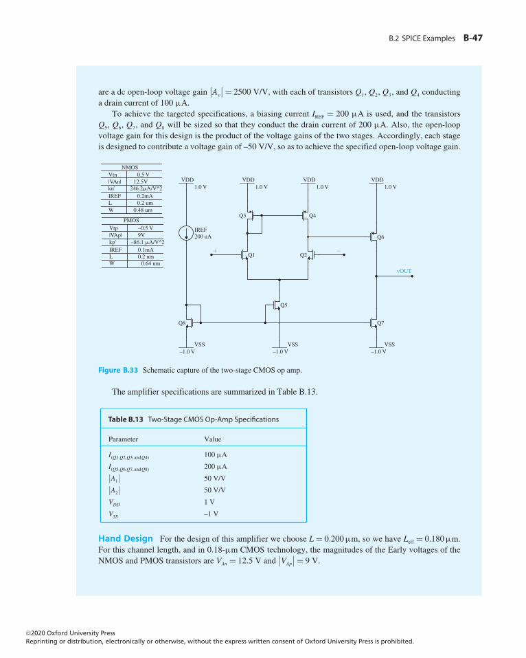
B.2 SPICE Examples B-47
are a dc open-loop voltage gain∣∣Av
∣∣ = 2500 V/V, with each of transistors Q1, Q2, Q3, and Q4 conductinga drain current of 100 µA.
To achieve the targeted specifications, a biasing current IREF = 200 µA is used, and the transistorsQ5, Q6, Q7, and Q8 will be sized so that they conduct the drain current of 200 µA. Also, the open-loopvoltage gain for this design is the product of the voltage gains of the two stages. Accordingly, each stageis designed to contribute a voltage gain of –50 V/V, so as to achieve the specified open-loop voltage gain.
Q1 Q2
Q3 Q4
Q6IREF200 uA
Q8
Q5
Q7
VDD1.0 V
VSS–1.0 V
VDD1.0 V
VDD1.0 V
VDD1.0 V
VSS–1.0 V
VSS–1.0 V
NMOSVtn|VAn|kn'IREFLW
0.5 V12.5V
246.2�A/V^20.2mA0.2 um
0.48 um
PMOSVtp|VAp|kp'IREFLW
–0.5 V9V
–86.1 �A/V^20.1mA0.2 um
0.64 um
� �
vOUT
Figure B.33 Schematic capture of the two-stage CMOS op amp.
The amplifier specifications are summarized in Table B.13.
Table B.13 Two-Stage CMOS Op-Amp Specifications
Parameter Value
I(Q1,Q2,Q3,andQ4) 100 µA
I(Q5,Q6,Q7,andQ8) 200 µA∣∣A1
∣∣ 50 V/V∣∣A2
∣∣ 50 V/V
VDD 1 V
VSS –1 V
Hand Design For the design of this amplifier we choose L= 0.200µm, so we have Leff = 0.180µm.For this channel length, and in 0.18-µm CMOS technology, the magnitudes of the Early voltages of theNMOS and PMOS transistors are VAn = 12.5 V and
∣∣VAp
∣∣ = 9 V.
©20 Oxford University PressReprinting or distribution, electronically or otherwise, without the express written consent of Oxford University Press is prohibited.
20
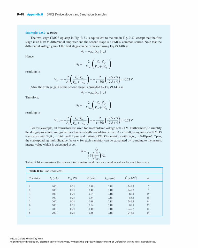
B-48 Appendix B SPICE Device Models and Simulation Examples
Example S.9.2 continued
The two-stage CMOS op amp in Fig. B.33 is equivalent to the one in Fig. 9.37, except that the firststage is an NMOS differential amplifier and the second stage is a PMOS common source. Note that thedifferential voltage gain of the first stage can be expressed using Eq. (9.140) as:
A1 = −gm1(ro2‖ro4
)Hence,
A1 = − 2
VOV 1
(VAn
∣∣VAp∣∣VAn +
∣∣VAp∣∣)
resulting in
VOV1 = − 2
A1
(VAn
∣∣VAp∣∣VAn +
∣∣VAp∣∣)
= − 2
(−50)
(12.5× 9
12.5+ 9
)� 0.21V
Also, the voltage gain of the second stage is provided by Eq. (9.141) as
A2 = −gm6(ro6‖ro7
)Therefore,
A2 = − 2
VOV 6
(VAn
∣∣VAp∣∣VAn +
∣∣VAp∣∣)
resulting in
VOV6 = − 2
A2
(VAn
∣∣VAp∣∣VAn +
∣∣VAp∣∣)
= − 2
(−50)
(12.5× 9
12.5+ 9
)� 0.21V
For this example, all transistors are sized for an overdrive voltage of 0.21 V. Furthermore, to simplifythe design procedure, we ignore the channel-length modulation effect. As a result, using unit-size NMOStransistors with Wn/Ln = 0.64µm/0.2µm, and unit-size PMOS transistors with Wn/Ln = 0.48µm/0.2µm,the corresponding multiplicative factor m for each transistor can be calculated by rounding to the nearestinteger value which is calculated as m:
m= ID1
2k ′
(W
Leff
)V2OV
Table B.14 summarizes the relevant information and the calculated m values for each transistor.
Table B.14 Transistor Sizes
Transistor ID (µA) VOV (V) W (µm) Leff (µm) k′(µA/V
2) m
1 100 0.21 0.48 0.18 246.2 72 100 0.21 0.48 0.18 246.2 73 100 0.21 0.64 0.18 86.1 154 100 0.21 0.64 0.18 86.1 155 200 0.21 0.48 0.18 246.2 146 200 0.21 0.64 0.18 86.1 307 200 0.21 0.48 0.18 246.2 148 200 0.21 0.48 0.18 246.2 14
©20 Oxford University PressReprinting or distribution, electronically or otherwise, without the express written consent of Oxford University Press is prohibited.
20
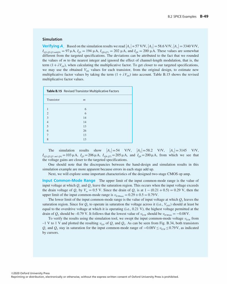
B.2 SPICE Examples B-49
Simulation
Verifying Av Based on the simulation results we read∣∣A1
∣∣ = 57 V/V,∣∣A2
∣∣= 58.6 V/V,∣∣Av
∣∣= 3340 V/V,I(Q1,Q2,Q3,andQ4) = 97µA, IQ5 = 194 µA, I(Q6,Q7) = 202 µA, and IQ8 = 200 µA. These values are somewhatdifferent from the targeted specifications. The deviations can be attributed to the fact that we roundedthe values of m to the nearest integer and ignored the effect of channel-length modulation, that is, theterm (1+λVDS), when calculating the multiplicative factor. To get closer to our targeted specifications,we may use the obtained VDS values for each transistor, from the original design, to estimate newmultiplicative factor values by taking the term (1+ λVDS) into account. Table B.15 shows the revisedmultiplicative factor values.
Table B.15 Revised Transistor Multiplicative Factors
Transistor m
1 62 63 144 145 136 267 138 13
The simulation results show∣∣A1
∣∣=54 V/V,∣∣A2
∣∣=58.2 V/V,∣∣Av
∣∣= 3145 V/V,I(Q1,Q2,Q3 and Q4) =103µA, IQ5 =206µA, I(Q6,Q7) =205µA, and IQ8 =200µA, from which we see thatthe voltage gains are closer to the targeted specifications.
One should note that the discrepancies between the hand-design and simulation results in thissimulation example are more apparent because errors in each stage add up.
Next, we will explore some important characteristics of the designed two-stage CMOS op amp.
Input Common-Mode Range The upper limit of the input common-mode range is the value ofinput voltage at which Q1 and Q2 leave the saturation region. This occurs when the input voltage exceedsthe drain voltage of Q1 by Vtn = 0.5 V. Since the drain of Q1 is at 1− (0.21+ 0.5) = 0.29 V, then theupper limit of the input common-mode range is vICMmax = 0.29+ 0.5= 0.79V.
The lower limit of the input common-mode range is the value of input voltage at which Q5 leaves thesaturation region. Since for Q5 to operate in saturation the voltage across it (i.e., VDS5) should at least beequal to the overdrive voltage at which it is operating (i.e., 0.21 V), the highest voltage permitted at thedrain of Q5 should be –0.79 V. It follows that the lowest value of vICM should be vICMmin = −0.08V.
To verify the results using the simulation tool, we swept the input common-mode voltage vICM from–1 V to 1 V and plotted the resulting vGD of Q1 and Q5. As can be seen from Fig. B.34, both transistorsQ1 and Q5 stay in saturation for the input common-mode range of −0.08V≤vICM ≤0.79V, as indicatedby cursors.
©20 Oxford University PressReprinting or distribution, electronically or otherwise, without the express written consent of Oxford University Press is prohibited.
20
B-50 Appendix B SPICE Device Models and Simulation Examples
Example S.9.2 continued
1.0
500.0 m
0
–500.0 m
–1.0
VG
D o
f Q
and
Q5
(V)
–1.5
–2.0–500 m 0
vv1 Voltage (V)
500 m–1
Q1 leavessaturation
Q5 leavessaturation
Figure B.34 Input common–mode range of the two-stage CMOS op amp.
Common-Mode Rejection Ratio (CMRR) of the First Stage The value of the CMRR of thefirst stage (the active-loaded MOS differential amplifier) is determined from Eq. (9.138). Note that thevalue of RSS in the provided equation corresponds to the output resistance of Q5 (i.e., ro5). Thus,
CMRR≡∣∣A1
∣∣∣∣Acm
∣∣ = 50
1/2gm3ro5= 100gm3ro5 = 100
2× 100× 10−6
0.21
12.5
200× 10−6 = 5952.4= 75.5 dB
Using the simulation tool, the value of CMRR is calculated by dividing the previously obtained A1 value(54 V/V) by the common-mode gain of the first stage. This yields
CMRR≡∣∣A1
∣∣∣∣Acm
∣∣ = 54
78× 10−3 = 6923= 76.8dB
Output Voltage Range The lowest allowable output voltage is the value at which Q7 leaves thesaturation region, which is −VSS +VOV7 = −1+0.21= 0.79V. The highest allowable output voltage is thevalue at which Q6 leaves saturation, which is VDD−∣∣−VOV6
∣∣ = 1−0.21= 0.79V. Thus, the output-voltagerange is –0.79 V to 0.79 V.
To verify the calculated output voltage range, we swept the input voltage from –2 mV to 2 mV (weused a small input voltage due to high gain). As can be seen from Fig. B.35, the output level changesfrom –0.795 V to 0.784 V, a rather symmetrical range. Therefore, the simulation results confirm ourhand-analysis calculations.
©20 Oxford University PressReprinting or distribution, electronically or otherwise, without the express written consent of Oxford University Press is prohibited.
20
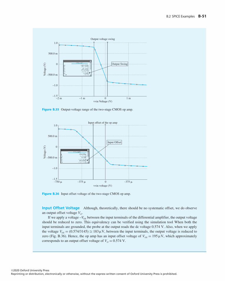
B.2 SPICE Examples B-51
1.0
Output voltage swing
500.0 m
–500.0 m
–1.0
–1.5–2 m –1 m 0
vvin Voltage (V)1 m
0
Vol
tage
(V
) Output Swing
Figure B.35 Output-voltage range of the two-stage CMOS op amp.
1.0Input offset of the op amp
500.0 m
–500.0 mVol
tage
(V
)
–1.0
–1.5–750 � –375 � –375 �0
vvin voltage (V)
0
Input Offset
Figure B.36 Input offset voltage of the two-stage CMOS op amp.
Input Offset Voltage Although, theoretically, there should be no systematic offset, we do observean output offset voltage VO.
If we apply a voltage –VOS between the input terminals of the differential amplifier, the output voltageshould be reduced to zero. This equivalency can be verified using the simulation tool When both theinput terminals are grounded, the probe at the output reads the dc voltage 0.574 V. Also, when we applythe voltage VOS = (0.574/3145) � 183µV, between the input terminals, the output voltage is reduced tozero (Fig. B.36). Hence, the op amp has an input offset voltage of VOS = 195µV, which approximatelycorresponds to an output offset voltage of VO = 0.574 V.
©20 Oxford University PressReprinting or distribution, electronically or otherwise, without the express written consent of Oxford University Press is prohibited.
20
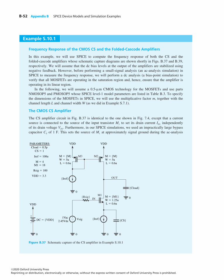
B-52 Appendix B SPICE Device Models and Simulation Examples
Example S.10.1
Frequency Response of the CMOS CS and the Folded-Cascode Amplifiers
In this example, we will use SPICE to compute the frequency response of both the CS and thefolded-cascode amplifiers whose schematic capture diagrams are shown shortly in Figs. B.37 and B.39,respectively. We will assume that the dc bias levels at the output of the amplifiers are stabilized usingnegative feedback. However, before performing a small-signal analysis (an ac-analysis simulation) inSPICE to measure the frequency response, we will perform a dc analysis (a bias-point simulation) toverify that all MOSFETs are operating in the saturation region and, hence, ensure that the amplifier isoperating in its linear region.
In the following, we will assume a 0.5-µm CMOS technology for the MOSFETs and use partsNMOSOP5 and PMOSOP5 whose SPICE level-1 model parameters are listed in Table B.3. To specifythe dimensions of the MOSFETs in SPICE, we will use the multiplicative factor m, together with thechannel length L and channel width W (as we did in Example S.7.1).
The CMOS CS Amplifier
The CS amplifier circuit in Fig. B.37 is identical to the one shown in Fig. 7.4, except that a currentsource is connected to the source of the input transistor M1 to set its drain current ID1 independentlyof its drain voltage VD1. Furthermore, in our SPICE simulations, we used an impractically large bypasscapacitor CS of 1 F. This sets the source of M1 at approximately signal ground during the ac-analysis
0
PARAMETERS: Cload � 0.5p CS � 1
Iref � 100u
M � 4 M1 � 18
Rsig � 100
VDD � 3.3
VDD VDD
M � {M}W � 5u L � 0.6u
M � {M}W � 5u L � 0.6u
M � {M1}W � 1.25u L � 0.6uVDD
DC � {VDD}�
�
0 0
�
�
�
�
OUT
{Rsig}
0 0
M3 M2
{Iref}
�
�{Iref} {CS}
1Vac2.45Vdc
Vsig
M1IN 0
{Cload}
Figure B.37 Schematic capture of the CS amplifier in Example S.10.1
©20 Oxford University PressReprinting or distribution, electronically or otherwise, without the express written consent of Oxford University Press is prohibited.
20
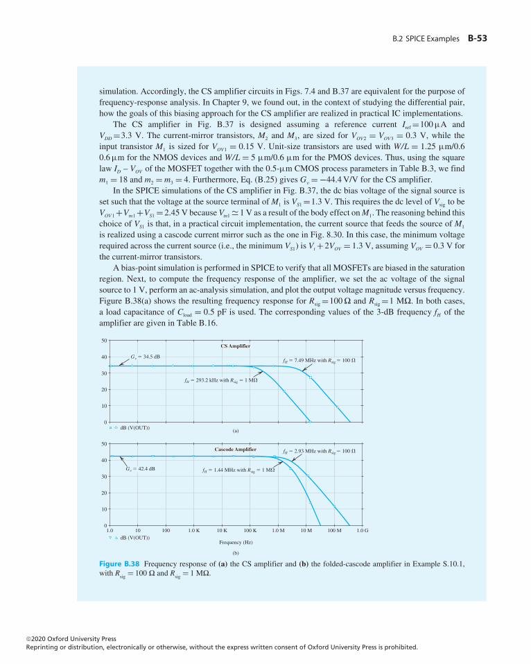
B.2 SPICE Examples B-53
simulation. Accordingly, the CS amplifier circuits in Figs. 7.4 and B.37 are equivalent for the purpose offrequency-response analysis. In Chapter 9, we found out, in the context of studying the differential pair,how the goals of this biasing approach for the CS amplifier are realized in practical IC implementations.
The CS amplifier in Fig. B.37 is designed assuming a reference current Iref =100µA andVDD=3.3 V. The current-mirror transistors, M2 and M3, are sized for VOV2 = VOV3 = 0.3 V, while theinput transistor M1 is sized for VOV1 = 0.15 V. Unit-size transistors are used with W/L = 1.25 µm/0.60.6µm for the NMOS devices and W/L = 5 µm/0.6 µm for the PMOS devices. Thus, using the squarelaw ID – VOV of the MOSFET together with the 0.5-µm CMOS process parameters in Table B.3, we findm1 = 18 and m2 =m3 = 4. Furthermore, Eq. (B.25) gives Gv = −44.4V/V for the CS amplifier.
In the SPICE simulations of the CS amplifier in Fig. B.37, the dc bias voltage of the signal source isset such that the voltage at the source terminal ofM1 is VS1 =1.3 V. This requires the dc level of Vsig to beVOV 1+Vtn1+VS1 = 2.45 V because Vtn1 � 1 V as a result of the body effect onM1. The reasoning behind thischoice of VS1 is that, in a practical circuit implementation, the current source that feeds the source of M1
is realized using a cascode current mirror such as the one in Fig. 8.30. In this case, the minimum voltagerequired across the current source (i.e., the minimum VS1) is Vt +2VOV = 1.3 V, assuming VOV = 0.3 V forthe current-mirror transistors.
A bias-point simulation is performed in SPICE to verify that all MOSFETs are biased in the saturationregion. Next, to compute the frequency response of the amplifier, we set the ac voltage of the signalsource to 1 V, perform an ac-analysis simulation, and plot the output voltage magnitude versus frequency.Figure B.38(a) shows the resulting frequency response for Rsig =100� and Rsig =1 M�. In both cases,a load capacitance of Cload = 0.5 pF is used. The corresponding values of the 3-dB frequency fH of theamplifier are given in Table B.16.
Figure B.38 Frequency response of (a) the CS amplifier and (b) the folded-cascode amplifier in Example S.10.1,with Rsig = 100 � and Rsig = 1 M�.
©20 Oxford University PressReprinting or distribution, electronically or otherwise, without the express written consent of Oxford University Press is prohibited.
20
B-54 Appendix B SPICE Device Models and Simulation Examples
Example S.10.1 continued
Table B.16 Dependence of the 3-dB Bandwidth fH on Rsig for the CS and the Folded-Cascode
Amplifiers in Example S.10.1
fH
Rsig CS Amplifier Folded-Cascode Amplifier
100� 7.49 MHz 2.93 MHz1 M� 293.2 kHz 1.44 MHz
Observe that fH drops when Rsig is increased. This is anticipated from our study of the high-frequencyresponse of the CS amplifier in Section 10.2. Specifically, as Rsig increases, the pole
fp, in = 1
2π
1
RsigCin
(B.27)
formed at the amplifier input will have an increasingly significant effect on the overall frequencyresponse of the amplifier. As a result, the effective time constant τH in Eq. (10.80) increases and fHdecreases. When Rsig becomes very large, as it is when Rsig = 1 M�, a dominant pole is formed by Rsig
and Cin. This results in
fH � fp, in (B.28)
To estimate fp, in, we need to calculate the input capacitance Cin of the amplifier. Using Miller’s theorem,we have
Cin = Cgs1 +Cgd1(1+ gm1R′L)
=(2
3m1W1L1Cox +Cgs,ov1
)+Cgd,ov1(1+ gm1R
′L) (B.29)
where
R′L = ro1‖ro2 (B.30)
Thus, Cin can be calculated using the values of Cgs1 and Cgd1, which are computed by SPICE and can befound in the output file of the bias-point simulation. Alternatively, Cin can be found using Eq. (B.29) withthe values of the overlap capacitances Cgs,ov1 and Cgsd,ov1 calculated using the process parameters in TableB.4 (as described in Eqs. B.9 and B.10); that is:
Cgs,ov1 =m1W1CGSO (B.31)
Cgd,ov1 =m1W1CGDO (B.32)
This results in Cin = 0.53 pF when∣∣Gv
∣∣ = gm1R′L = 53.2V/V. Accordingly, using Eqs. (B.27) and (B.28),
fH = 300.3 kHz when Rsig = 1 M�, which is close to the value computed by SPICE.
The Folded-Cascode Amplifier
The folded-cascode amplifier circuit in Fig. B.39 is equivalent to the one in Fig. 13.8, except that a currentsource is placed in the source of the input transistorM1 (for the same dc-biasing purpose as in the case of
©20 Oxford University PressReprinting or distribution, electronically or otherwise, without the express written consent of Oxford University Press is prohibited.
20
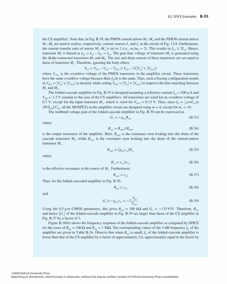
B.2 SPICE Examples B-55
the CS amplifier). Note that, in Fig. B.39, the PMOS current mirrorM3–M4 and the NMOS current mirrorM5–M6 are used to realize, respectively, current sources I1 and I2 in the circuit of Fig. 13.8. Furthermore,the current transfer ratio of mirror M3–M4 is set to 2 (i.e., m3/m4 = 2). This results in ID3 � 2Iref. Hence,transistor M2 is biased at ID2 = ID3 − ID1 = Iref. The gate bias voltage of transistor M2 is generated usingthe diode-connected transistorsM7 andM8. The size and drain current of these transistors are set equal tothose of transistor M2. Therefore, ignoring the body effect,
VG2 = VDD −VSG7 −VSG8 � VDD − 2(∣∣Vtp∣∣+ ∣∣VOVp∣∣)
where VOVp is the overdrive voltage of the PMOS transistors in the amplifier circuit. These transistorshave the same overdrive voltage because their ID/m is the same. Thus, such a biasing configuration resultsin VSG2 = ∣∣Vtp∣∣+ ∣∣VOVp∣∣ as desired, while setting VSD3 = ∣∣Vtp∣∣+ ∣∣VOVp∣∣ to improve the bias matching betweenM3 andM4.
The folded-cascode amplifier in Fig. B.39 is designed assuming a reference current Iref =100 µA andVDD = 3.3 V (similar to the case of the CS amplifier). All transistors are sized for an overdrive voltage of0.3 V, except for the input transistor M1, which is sized for VOV1 = 0.15 V. Thus, since ID = 1
2μmCoxm(
W/Leff
)V2OV , all the MOSFETs in the amplifier circuit are designed using m= 4, except for m1 = 18.
The midband voltage gain of the folded-cascode amplifier in Fig. B.39 can be expressed as
Gv = −gm1Rout (B.33)
where
Rout = Rout2‖Rout5 (B.34)
is the output resistance of the amplifier. Here, Rout2 is the resistance seen looking into the drain of thecascode transistor M2, while Rout5 is the resistance seen looking into the drain of the current-mirrortransistor M5.
Rout2 � (gm2ro2
)Rs2 (B.35)
where
Rs2 = ro1‖ro3 (B.36)
is the effective resistance at the source ofM2. Furthermore,
Rout5 = ro5 (B.37)
Thus, for the folded-cascoded amplifier in Fig. B.39,
Rout � ro5 (B.38)
and
Gv �−gm1ro5 = −2VAnVOV1
(B.39)
Using the 0.5-µm CMOS parameters, this gives Rout = 100 k� and Gv = −133V/V. Therefore, Rout
and hence∣∣Gv
∣∣ of the folded-cascode amplifier in Fig. B.39 are larger than those of the CS amplifier inFig. B.37 by a factor of 3.
Figure B.38(b) shows the frequency response of the folded-cascode amplifier as computed by SPICEfor the cases of Rsig = 100� and Rsig = 1 M�. The corresponding values of the 3-dB frequency fH of theamplifier are given in Table B.16. Observe that when Rsig is small, fH of the folded-cascode amplifier islower than that of the CS amplifier by a factor of approximately 2.6, approximately equal to the factor by
©20 Oxford University PressReprinting or distribution, electronically or otherwise, without the express written consent of Oxford University Press is prohibited.
20
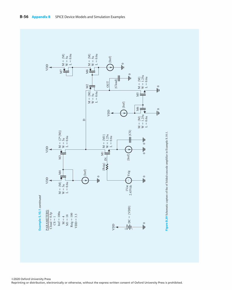
B-56 Appendix B SPICE Device Models and Simulation Examples
0
PAR
AM
ETER
S: C
load
0
.5p
CS
1
Ir
ef
100
u
M
4
M1
18
R
sig
100
V
DD
3
.3
VD
DV
DD
VD
D
VD
D
M
{M
}W
5
u L
0
.6u
M
{2*
{M}}
W
5u
L
0.6
u
M
{M
1}W
1
.25u
L
0.6
u
M
{M
}W
1
.25u
L
0.6
u
M
{M
}W
1
.25u
L
0.6
u
M
{M
}W
5
u L
0
.6u
M
{M
}W
5
u L
0
.6u
M
{M
}W
5
u L
0
.6u
VD
D
DC
{
VD
D}
00
D
{Rsi
g}
0
0
0
M4
M3
{Ire
f}
{Ire
f}
0{Ire
f}
{Ire
f}
{CS}
1Vac
2.45
Vdc
Vsi
g
M1
M7
M2
M8
M6
M5
IN
0
0
{Clo
ad}
OU
T
Figu
re B
.39
Sche
mat
ic c
aptu
re o
f the
of f
olde
d-ca
scod
e am
plifi
er in
Exa
mpl
e S.
10.1
.
Exam
ple
S.1
0.1 continued
©20 Oxford University PressReprinting or distribution, electronically or otherwise, without the express written consent of Oxford University Press is prohibited.
20
B.2 SPICE Examples B-57
which the gain is increased. This is because when Rsig is small, the frequency response of both amplifiersis dominated by the pole formed at the output node, that is,
fH � fp,out =1
2π
1
RoutCout
(B.40)
Since the output resistance of the folded-cascode amplifier is larger than that of the CS amplifier (by afactor of approximately 3, as found through the hand analysis above) while their output capacitances areapproximately equal, the folded-cascode amplifier has a lower fH in this case.
On the other hand, when Rsig is large, fH of the folded-cascode amplifier is much higher than thatof the CS amplifier. This is because, in this case, the effect of the pole at fp, in on the overall frequencyresponse of the amplifier becomes significant. Since, due to the Miller effect, Cin of the CS amplifier ismuch larger than that of the folded-cascode amplifier, its fH is much lower in this case. To confirm thispoint, observe that Cin of the folded-cascode amplifier can be estimated by replacing R′
L in Eq. (B.29) withthe total resistance Rd1 between the drain of M1 and ground. Here,
Rd1 = ro1‖ro3‖Rin2 (B.41)
where Rin2 is the input resistance of the common-gate transistor M2 and can be obtained using anapproximation of the relationship in Eq. (8.51) as
Rin2 � ro2 + ro5gm2ro2
(B.42)
Thus,
Rd1 � ro1‖ro3‖(ro2 + ro5gm2ro2
� 2
gm2
)(B.43)
Therefore, Rd1 is much smaller than R′L in Eq. (B.30). Hence, Cin of the folded-cascode amplifier in
Fig. B.39 is indeed much smaller than that of the CS amplifier in Fig. B.37. This confirms that thefolded-cascode amplifier is much less impacted by the Miller effect and, therefore, can achieve a muchhigher fH when Rsig is large.
The midband gain of the folded-cascode amplifier can be significantly increased by replacing thecurrent mirrorM5–M6 with a current mirror having a larger output resistance, such as the cascode currentmirror in Fig. 8.36 whose output resistance is approximately gmr
2o . In this case, however, Rin2 and hence
Rd1 increase, causing an increased Miller effect and a corresponding reduction in fH .Finally, it is interesting to observe that the frequency response of the folded-cascode amplifier,
shown in Fig. B.38(b), drops beyond fH at approximately –20 dB/decade when Rsig =100� and atapproximately −40 dB/decade when Rsig =1 M�. This is because when Rsig is small, the frequencyresponse is dominated by the pole at fp,out. However, when Rsig is increased, fp, in is moved closer to fp,outand both poles contribute to the gain falloff.
©20 Oxford University PressReprinting or distribution, electronically or otherwise, without the express written consent of Oxford University Press is prohibited.
20
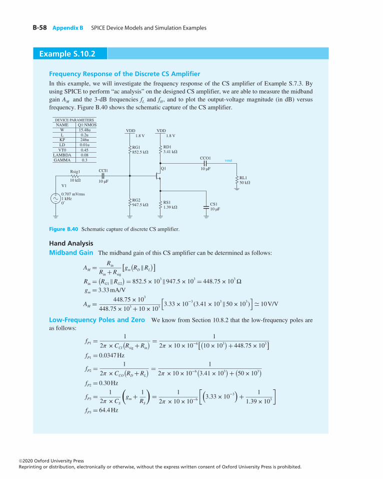
B-58 Appendix B SPICE Device Models and Simulation Examples
Example S.10.2
Frequency Response of the Discrete CS AmplifierIn this example, we will investigate the frequency response of the CS amplifier of Example S.7.3. Byusing SPICE to perform “ac analysis” on the designed CS amplifier, we are able to measure the midbandgain AM and the 3-dB frequencies fL and fH , and to plot the output-voltage magnitude (in dB) versusfrequency. Figure B.40 shows the schematic capture of the CS amplifier.
NAME
WL
KPLDVT0
LAMBDAGAMMA
DEVICE PARAMETERSQ1:NMOS15.48u0.2u
0.01u0.450.080.3
246u
RG1852.5 k�
RD13.41 k�
RG2947.5 k�
RL150 k�
Rsig1
10 k�
CCI1
10 µF
CCO1
10 µF
CS110 µF
VDD1.8 V
VDD1.8 V
V1
0.707 mVrms 1 kHz 0˚ RS1
1.39 k�
vout
Q1
�
�
Figure B.40 Schematic capture of discrete CS amplifier.
Hand AnalysisMidband Gain The midband gain of this CS amplifier can be determined as follows:
AM = Rin
Rin +Rsig
[gm
(RD‖RL
)]Rin = (
RG1‖RG2
) = 852.5× 10³‖947.5× 103 = 448.75× 10³�
gm = 3.33mA/V
AM = 448.75× 10³
448.75× 10³ + 10× 103
[3.33× 10⁻³
(3.41× 10³‖50× 103)]
� 10V/V
Low-Frequency Poles and Zero We know from Section 10.8.2 that the low-frequency poles areas follows:
fP1 = 1
2π ×CCI
(Rsig +Rin
) = 1
2π × 10× 10−6[(10× 103
)+ 448.75× 10³]
fP1 = 0.0347Hz
fP2 = 1
2π ×CCO
(RD +RL
) = 1
2π × 10× 10−6(3.41× 10³
)+ (50× 103
)fP2 = 0.30Hz
fP3 = 1
2π ×CS
(gm + 1
RS
)= 1
2π × 10× 10−6
[(3.33× 10⁻³
)+ 1
1.39× 10³
]fP3 = 64.4Hz
©20 Oxford University PressReprinting or distribution, electronically or otherwise, without the express written consent of Oxford University Press is prohibited.
20
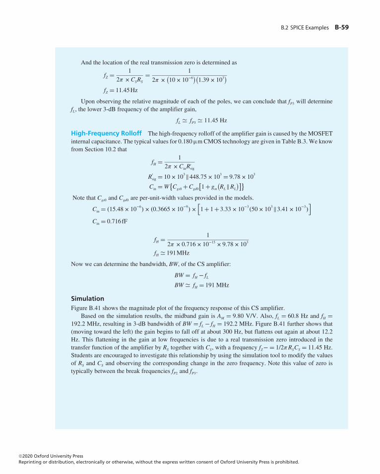
B.2 SPICE Examples B-59
And the location of the real transmission zero is determined as
fZ = 1
2π ×CSRS
= 1
2π × (10× 10−6
)(1.39× 10³
)fZ = 11.45Hz
Upon observing the relative magnitude of each of the poles, we can conclude that fP3 will determinefL, the lower 3-dB frequency of the amplifier gain,
fL � fP3 � 11.45 Hz
High-Frequency Rolloff The high-frequency rolloff of the amplifier gain is caused by the MOSFETinternal capacitance. The typical values for 0.180µmCMOS technology are given in Table B.3. We knowfrom Section 10.2 that
fH = 1
2π ×CinR′sig
R′sig = 10× 103‖448.75× 103 = 9.78× 10³
Cin =W{Cgs0 +Cgd0
[1+ gm
(RL‖RL
)]}Note that Cgs0 and Cgd0 are per-unit-width values provided in the models.
Cin = (15.48× 10−6)× (0.3665× 10−9
)×[1+ 1+ 3.33× 10⁻³
(50× 103‖3.41× 10⁻³)]
Cin = 0.716fF
fH = 1
2π × 0.716× 10−15 × 9.78× 103
fH � 191MHz
Now we can determine the bandwidth, BW, of the CS amplifier:
BW = fH − fLBW � fH = 191 MHz
SimulationFigure B.41 shows the magnitude plot of the frequency response of this CS amplifier.
Based on the simulation results, the midband gain is AM = 9.80 V/V. Also, fL = 60.8 Hz and fH =192.2 MHz, resulting in 3-dB bandwidth of BW = fL − fH = 192.2 MHz. Figure B.41 further shows that(moving toward the left) the gain begins to fall off at about 300 Hz, but flattens out again at about 12.2Hz. This flattening in the gain at low frequencies is due to a real transmission zero introduced in thetransfer function of the amplifier by RS together with CS, with a frequency fZ− = 1/2πRSCS = 11.45 Hz.Students are encouraged to investigate this relationship by using the simulation tool to modify the valuesof RS and CS and observing the corresponding change in the zero frequency. Note this value of zero istypically between the break frequencies fP2 and fP3.
©20 Oxford University PressReprinting or distribution, electronically or otherwise, without the express written consent of Oxford University Press is prohibited.
20
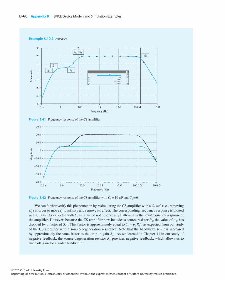
B-60 Appendix B SPICE Device Models and Simulation Examples
Example S.10.2 continued
30
20
10
–10
–20
–30
–4010 m 1 100 10 k
Frequency (Hz)
1 M 100 M 10 G
0
Mag
nitu
de fP1
fP2
fH
fz
fP2 = fL
Figure B.41 Frequency response of the CS amplifier.
30.0
20.0
10.0
�10.0
�20.0
�30.0
�40.010.0 m 1.0 100.0 10.0 k
Frequency (Hz)
1.0 M 100.0 M 10.0 G
0
Mag
nitu
de
Figure B.42 Frequency response of the CS amplifier with CS=10 µF and CS=0.
We can further verify this phenomenon by resimulating the CS amplifier with a CS = 0 (i.e., removingCS) in order to move fZ to infinity and remove its effect. The corresponding frequency response is plottedin Fig. B.42. As expected with CS = 0, we do not observe any flattening in the low-frequency response ofthe amplifier. However, because the CS amplifier now includes a source resistor RS, the value of AM hasdropped by a factor of 5.4. This factor is approximately equal to (1+ gmRS), as expected from our studyof the CS amplifier with a source-degeneration resistance. Note that the bandwidth BW has increasedby approximately the same factor as the drop in gain AM . As we learned in Chapter 11 in our study ofnegative feedback, the source-degeneration resistor RS provides negative feedback, which allows us totrade off gain for a wider bandwidth.
©20 Oxford University PressReprinting or distribution, electronically or otherwise, without the express written consent of Oxford University Press is prohibited.
20
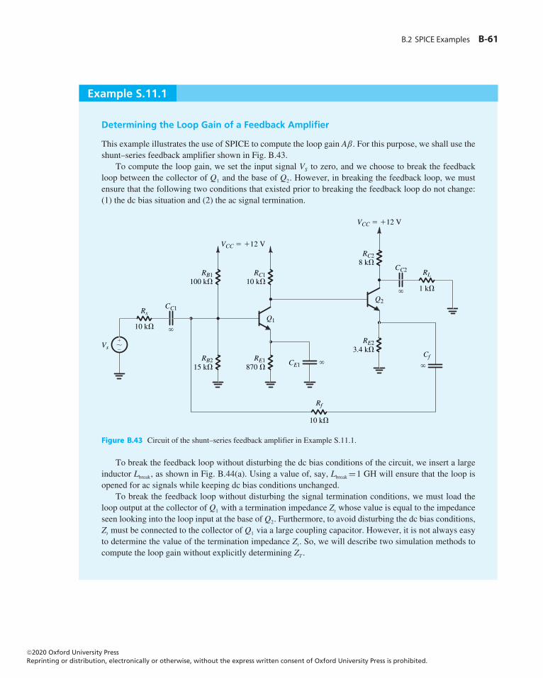
B.2 SPICE Examples B-61
Example S.11.1
Determining the Loop Gain of a Feedback Amplifier
This example illustrates the use of SPICE to compute the loop gain Aβ. For this purpose, we shall use theshunt–series feedback amplifier shown in Fig. B.43.
To compute the loop gain, we set the input signal VS to zero, and we choose to break the feedbackloop between the collector of Q1 and the base of Q2. However, in breaking the feedback loop, we mustensure that the following two conditions that existed prior to breaking the feedback loop do not change:(1) the dc bias situation and (2) the ac signal termination.
Q2
Cf
CC2 RL
RC28 k�
1 k�
VCC � �12 V
RE23.4 k�
Q1
RC110 k�
VCC � �12 V
RE1870 �
Rs
10 k�
CC1
RB1100 k�
RB215 k�
CE1
Vs�
�
Rf
10 k�
Figure B.43 Circuit of the shunt–series feedback amplifier in Example S.11.1.
To break the feedback loop without disturbing the dc bias conditions of the circuit, we insert a largeinductor Lbreak, as shown in Fig. B.44(a). Using a value of, say, Lbreak =1 GH will ensure that the loop isopened for ac signals while keeping dc bias conditions unchanged.
To break the feedback loop without disturbing the signal termination conditions, we must load theloop output at the collector of Q1 with a termination impedance Zt whose value is equal to the impedanceseen looking into the loop input at the base of Q2. Furthermore, to avoid disturbing the dc bias conditions,Zt must be connected to the collector of Q1 via a large coupling capacitor. However, it is not always easyto determine the value of the termination impedance Zt. So, we will describe two simulation methods tocompute the loop gain without explicitly determining ZT .
©20 Oxford University PressReprinting or distribution, electronically or otherwise, without the express written consent of Oxford University Press is prohibited.
20
B-62 Appendix B SPICE Device Models and Simulation Examples
Example S.11.1 continued
Method 1 Using the open-circuit and short-circuit transfer functionsNote that to avoid the problem of terminating the loop when we open it, the loop gain can be expressedas
Aβ = −1/(
1
Toc+ 1
Tsc
)
where Toc is the open-circuit voltage transfer function and Tsc is the short-circuit voltage transfer function.The circuit for determining Toc is shown in Fig. B.44(b). Here, an ac test signal voltage Vt is applied
to the loop input at the base of Q2 via a large coupling capacitor (having a value of, say, 1 kF) to avoiddisturbing the dc bias conditions. Then,
Toc = VocVt
where Voc is the ac open-circuit output voltage at the collector of Q1.In the circuit for determining Tsc (Fig. B.44b), an ac test signal current It is applied to the loop input
at the base of Q2. Note that a coupling capacitor is not needed in this case because the ac current sourceappears as an open circuit at dc, and, hence, does not disturb the dc bias conditions.
The loop output at the collector of Q1 is ac short-circuited to ground via a large capacitor Cto. Then,
Tsc = IscIt
where Isc is the ac short-circuit output current at the collector of Q1.
Method 2 Using a replica circuitAs shown in Fig. B.45, a replica of the feedback amplifier circuit can be simply used as a terminationimpedance. Here, the feedback loops of both the amplifier circuit and the replica circuit are broken usinga large inductor Lbreak to avoid disturbing the dc bias conditions. The loop output at the collector of Q1
in the amplifier circuit is then connected to the loop input at the base of Q2 in the replica circuit via alarge coupling capacitor Cto (again, to avoid disturbing the dc bias conditions). Thus, for ac signals, theloop output at the collector of Q1 in the amplifier circuit sees an impedance equal to that seen before thefeedback loop is broken. Accordingly, we have ensured that the conditions that existed in the amplifiercircuit prior to breaking the loop have not changed.
Next, to determine the loop gain Aβ, we apply an ac test signal voltage Vt via a large couplingcapacitor Cti to the loop input at the base of Q2 in the amplifier circuit. Then, as described in Chapter 11,
Aβ = −VrVt
where Vr is the ac returned signal at the loop output at the collector of Q1 in the amplifier circuit.
©20 Oxford University PressReprinting or distribution, electronically or otherwise, without the express written consent of Oxford University Press is prohibited.
20
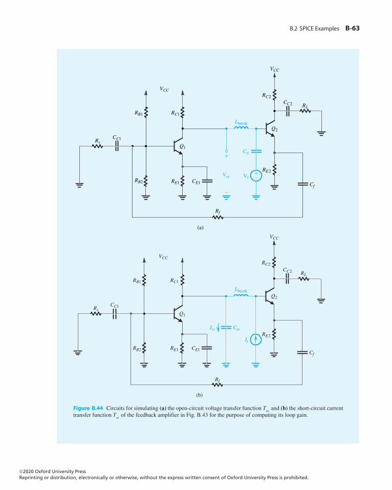
B.2 SPICE Examples B-63
(a)
Q2
Cf
CC2 RL
RC2
VCC
Rf
RE2
Q1
RC1
VCC
RE1
RsCC1
RB1
RB2 CE1
Cti�
�
Voc
Lbreak
Vt��
(b)
Q2
Cf
CC2 RL
RC2
Rf
RE2
Q1
RC1
VCC
RE1
RsCC1
RB1
RB2 CE1
Isc Cto
It
Lbreak
VCC
Figure B.44 Circuits for simulating (a) the open-circuit voltage transfer function Toc and (b) the short-circuit currenttransfer function Tsc of the feedback amplifier in Fig. B.43 for the purpose of computing its loop gain.
©20 Oxford University PressReprinting or distribution, electronically or otherwise, without the express written consent of Oxford University Press is prohibited.
20
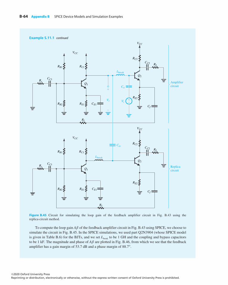
B-64 Appendix B SPICE Device Models and Simulation Examples
Example S.11.1 continued
Q2
Cf
CC2 RL
RC2
VCC
Rf
RE2
Q1
RC1
VCC
RE1
RsCC1
RB1
RB2 CE1
Cti�
�
Vr
Lbreak
Q2
Cf
CC2 RL
RC2
VCC
Rf
RE2
Q1
RC1
VCC
RE1
RsCC1
RB1
RB2 CE1
Lbreak
Cto
Amplifiercircuit
Replicacircuit
Vt��
Figure B.45 Circuit for simulating the loop gain of the feedback amplifier circuit in Fig. B.43 using thereplica-circuit method.
To compute the loop gain Aβ of the feedback amplifier circuit in Fig. B.43 using SPICE, we choose tosimulate the circuit in Fig. B.45. In the SPICE simulations, we used part Q2N3904 (whose SPICE modelis given in Table B.6) for the BJTs, and we set Lbreak to be 1 GH and the coupling and bypass capacitorsto be 1 kF. The magnitude and phase of Aβ are plotted in Fig. B.46, from which we see that the feedbackamplifier has a gain margin of 53.7 dB and a phase margin of 88.7°.
©20 Oxford University PressReprinting or distribution, electronically or otherwise, without the express written consent of Oxford University Press is prohibited.
20
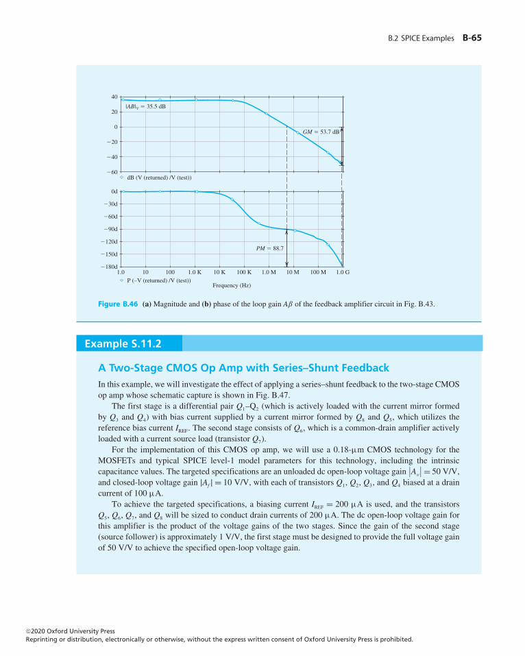
B.2 SPICE Examples B-65
�60
�40
�20
0
20
dB (V (returned) /V (test))
40
Frequency (Hz)
1.0 1.0 G100 M10 M 1.0 M100 K10 K1.0 K10010
�150d
�120d
�90d
�60d
�30d
P (–V (returned) /V (test))
0d
�180d
|AB|V � 35.5 dB
PM � 88.7
GM � 53.7 dB
Figure B.46 (a) Magnitude and (b) phase of the loop gain Aβ of the feedback amplifier circuit in Fig. B.43.
Example S.11.2
A Two-Stage CMOS Op Amp with Series–Shunt FeedbackIn this example, we will investigate the effect of applying a series–shunt feedback to the two-stage CMOSop amp whose schematic capture is shown in Fig. B.47.
The first stage is a differential pair Q1–Q2 (which is actively loaded with the current mirror formedby Q3 and Q4) with bias current supplied by a current mirror formed by Q8 and Q5, which utilizes thereference bias current IREF. The second stage consists of Q6, which is a common-drain amplifier activelyloaded with a current source load (transistor Q7).
For the implementation of this CMOS op amp, we will use a 0.18-µm CMOS technology for theMOSFETs and typical SPICE level-1 model parameters for this technology, including the intrinsiccapacitance values. The targeted specifications are an unloaded dc open-loop voltage gain
∣∣Av
∣∣ = 50 V/V,and closed-loop voltage gain |Af | = 10 V/V, with each of transistors Q1, Q2, Q3, and Q4 biased at a draincurrent of 100 µA.
To achieve the targeted specifications, a biasing current IREF = 200 µA is used, and the transistorsQ5, Q6, Q7, and Q8 will be sized to conduct drain currents of 200 µA. The dc open-loop voltage gain forthis amplifier is the product of the voltage gains of the two stages. Since the gain of the second stage(source follower) is approximately 1 V/V, the first stage must be designed to provide the full voltage gainof 50 V/V to achieve the specified open-loop voltage gain.
©20 Oxford University PressReprinting or distribution, electronically or otherwise, without the express written consent of Oxford University Press is prohibited.
20
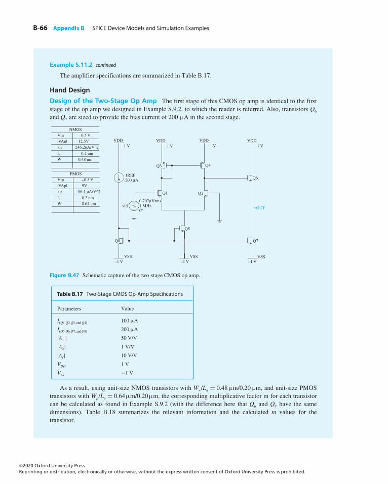
B-66 Appendix B SPICE Device Models and Simulation Examples
Example S.11.2 continued
The amplifier specifications are summarized in Table B.17.
Hand Design
Design of the Two-Stage Op Amp The first stage of this CMOS op amp is identical to the firststage of the op amp we designed in Example S.9.2, to which the reader is referred. Also, transistors Q6
and Q7 are sized to provide the bias current of 200 µA in the second stage.
VDD VDD VDD VDD1 V
1REF 200 μA
Q3
Q1 Q2
Q5
Q8
Q4
1 V 1 V
Q6
Q7
vOUT
VSS–1 V–1 V–1 V
VSSVSS
1 V
vid0.707μVrms 1 MHz 0º
�
�
NMOSVtn|VAn|kn'
LW
0.5 V12.5V
246.2uA/V^2
0.2 um0.48 um
PMOSVtp|VAp|kp'
LW
–0.5 V9V
–86.1 µA/V^2
0.2 um0.64 um
Figure B.47 Schematic capture of the two-stage CMOS op amp.
Table B.17 Two-Stage CMOS Op-Amp Specifications
Parameters Value
I(Q1,Q2,Q3,andQ4) 100 µA
I(Q5,Q6,Q7,andQ8) 200 µA
|A1‖ 50 V/V
|A2| 1 V/V
|Af | 10 V/V
VDD 1 V
VSS −1 V
As a result, using unit-size NMOS transistors with Wn/Ln = 0.48µm/0.20µm, and unit-size PMOStransistors with Wp/Lp = 0.64µm/0.20µm, the corresponding multiplicative factor m for each transistorcan be calculated as found in Example S.9.2 (with the difference here that Q6 and Q7 have the samedimensions). Table B.18 summarizes the relevant information and the calculated m values for thetransistor.
©20 Oxford University PressReprinting or distribution, electronically or otherwise, without the express written consent of Oxford University Press is prohibited.
20
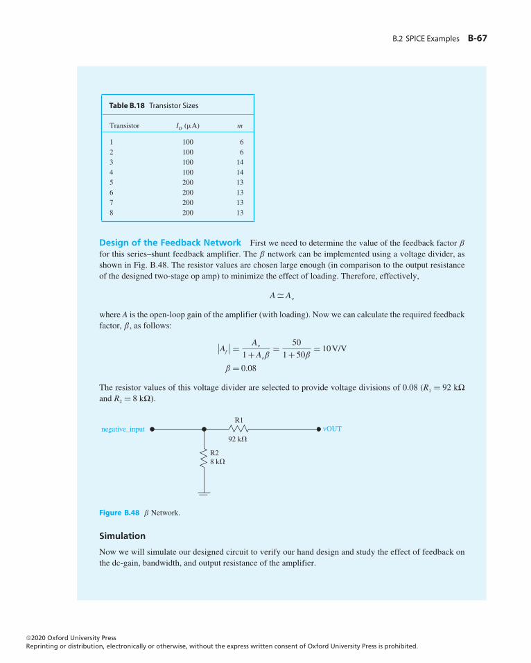
B.2 SPICE Examples B-67
Table B.18 Transistor Sizes
Transistor ID (µA) m
1 100 62 100 63 100 144 100 145 200 136 200 137 200 138 200 13
Design of the Feedback Network First we need to determine the value of the feedback factor β
for this series–shunt feedback amplifier. The β network can be implemented using a voltage divider, asshown in Fig. B.48. The resistor values are chosen large enough (in comparison to the output resistanceof the designed two-stage op amp) to minimize the effect of loading. Therefore, effectively,
A� Av
where A is the open-loop gain of the amplifier (with loading). Now we can calculate the required feedbackfactor, β, as follows:
∣∣Af
∣∣ = Av
1+Avβ= 50
1+ 50β= 10V/V
β = 0.08
The resistor values of this voltage divider are selected to provide voltage divisions of 0.08 (R1 = 92 k�and R2 = 8 k�).
vOUTnegative_inputR1
92 k�
R2 8 k�
Figure B.48 β Network.
Simulation
Now we will simulate our designed circuit to verify our hand design and study the effect of feedback onthe dc-gain, bandwidth, and output resistance of the amplifier.
©20 Oxford University PressReprinting or distribution, electronically or otherwise, without the express written consent of Oxford University Press is prohibited.
20
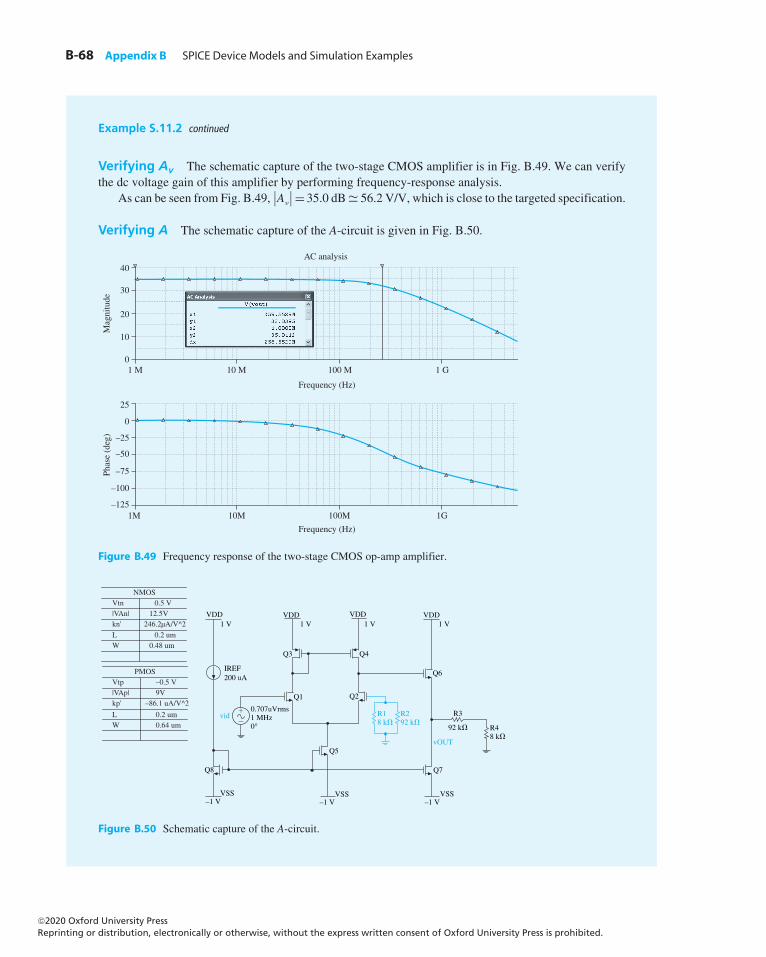
B-68 Appendix B SPICE Device Models and Simulation Examples
Example S.11.2 continued
Verifying Av The schematic capture of the two-stage CMOS amplifier is in Fig. B.49. We can verifythe dc voltage gain of this amplifier by performing frequency-response analysis.
As can be seen from Fig. B.49,∣∣Av
∣∣= 35.0 dB� 56.2 V/V, which is close to the targeted specification.
Verifying A The schematic capture of the A-circuit is given in Fig. B.50.
40AC analysis
30
20
Mag
nitu
dePh
ase
(deg
)
10
0
25
–25
–75
1M 10M 100M
Frequency (Hz)
1G
–100
–125
–50
0
1 M 10 M 100 M
Frequency (Hz)
1 G
Figure B.49 Frequency response of the two-stage CMOS op-amp amplifier.
VDD1 V 1 V 1 V 1 V
Q3
Q8
VSS VSS VSS–1 V–1 V–1 V
Q1
R18 k�
R3R292 k�
R48 k�
92 k�
Q5
Q7
0.707uVrms1 MHz0°
vid
Q2
Q6
vOUT
Q4
IREF200 uA
VDD VDD VDD
�
�
NMOSVtn|VAn|kn'
LW
0.5 V12.5V
246.2µA/V^2
0.2 um0.48 um
PMOSVtp|VAp|kp'
LW
–0.5 V9V
–86.1 uA/V^2
0.2 um0.64 um
Figure B.50 Schematic capture of the A-circuit.
©20 Oxford University PressReprinting or distribution, electronically or otherwise, without the express written consent of Oxford University Press is prohibited.
20
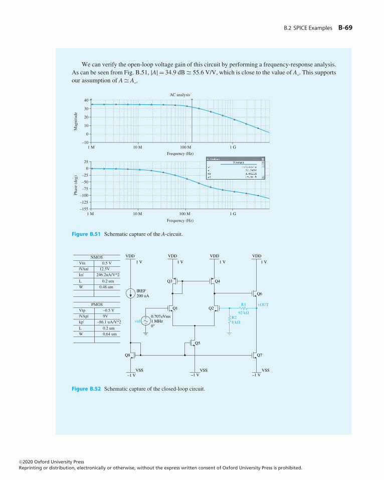
B.2 SPICE Examples B-69
We can verify the open-loop voltage gain of this circuit by performing a frequency-response analysis.As can be seen from Fig. B.51, |A| = 34.9 dB � 55.6 V/V, which is close to the value of Av. This supportsour assumption of A� Av.
40 AC analysis
30
20
10
–10 1 M
25
0
–25
–50
–75
–100 Phas
e (d
eg)
Mag
nitu
de
–125
–155
10 M 100 M
Frequency (Hz)
Frequency (Hz)
1 G
1 M 10 M 100 M 1 G
0
Figure B.51 Schematic capture of the A-circuit.
VDD VDD VDD VDD
Q3 Q4
Q1 Q2
Q6
vOUT
vid
R1
R28 k�
92 k�
Q5
Q7Q8
VSS VSS VSS–1 V –1 V –1 V
0.707uVms1 MHz0°
1 V 1 V 1 V 1 V
IREF200 uA
�
�
NMOSVtn|VAn|kn'
LW
0.5 V12.5V
246.2uA/V^2
0.2 um0.48 um
PMOSVtp|VAp|kp'
LW
–0.5 V9V
–86.1 uA/V^2
0.2 um0.64 um
Figure B.52 Schematic capture of the closed-loop circuit.
©20 Oxford University PressReprinting or distribution, electronically or otherwise, without the express written consent of Oxford University Press is prohibited.
20
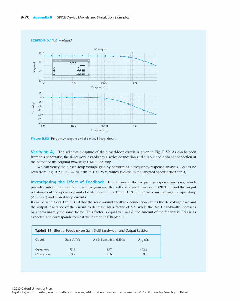
B-70 Appendix B SPICE Device Models and Simulation Examples
Example S.11.2 continued
25
AC analysis
10
Mag
nitu
de
–5
–20 1 M
25
–25
Phas
e (d
eg)
–50
–75
–100
–125
–150 1 M
0
10 M 100 M 1 G
Frequency (Hz)
10 M 100 M 1 G
Frequency (Hz)
Figure B.53 Frequency response of the closed-loop circuit.
Verifying Af The schematic capture of the closed-loop circuit is given in Fig. B.52. As can be seenfrom this schematic, the β-network establishes a series connection at the input and a shunt connection atthe output of the original two-stage CMOS op amp.
We can verify the closed-loop voltage gain by performing a frequency-response analysis. As can beseen from Fig. B.53,
∣∣Af
∣∣ = 20.2 dB � 10.2 V/V, which is close to the targeted specification for Af .
Investigating the Effect of Feedback In addition to the frequency-response analysis, whichprovided information on the dc voltage gain and the 3-dB bandwidth, we used SPICE to find the outputresistances of the open-loop and closed-loop circuits Table B.19 summarizes our findings for open-loop(A-circuit) and closed-loop circuits.It can be seen from Table B.19 that the series–shunt feedback connection causes the dc voltage gain andthe output resistance of the circuit to decrease by a factor of 5.5, while the 3-dB bandwidth increasesby approximately the same factor. This factor is equal to 1+Aβ, the amount of the feedback. This is asexpected and corresponds to what we learned in Chapter 11.
Table B.19 Effect of Feedback on Gain, 3-dB Bandwidth, and Output Resistor
Circuit Gain (V/V) 3-dB Bandwidth (MHz) Rout (�)
Open loop 55.6 137 492.6Closed loop 10.2 816 89.3
©20 Oxford University PressReprinting or distribution, electronically or otherwise, without the express written consent of Oxford University Press is prohibited.
20
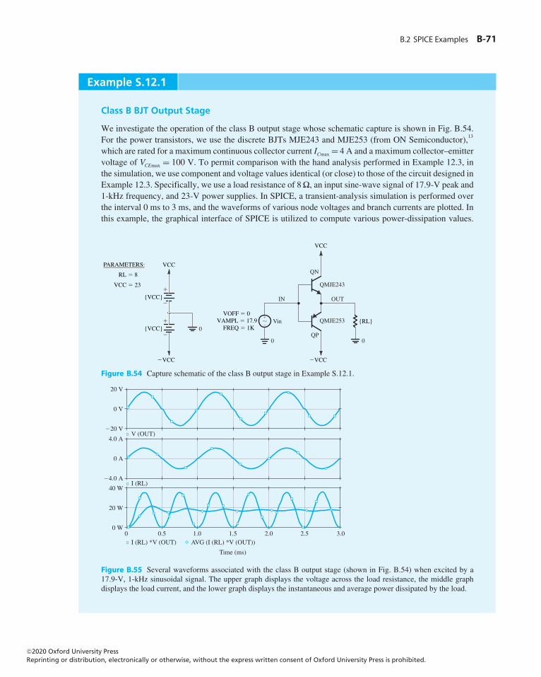
B.2 SPICE Examples B-71
Example S.12.1
Class B BJT Output Stage
We investigate the operation of the class B output stage whose schematic capture is shown in Fig. B.54.For the power transistors, we use the discrete BJTs MJE243 and MJE253 (from ON Semiconductor),13
which are rated for a maximum continuous collector current ICmax = 4 A and a maximum collector–emittervoltage of VCEmax = 100 V. To permit comparison with the hand analysis performed in Example 12.3, inthe simulation, we use component and voltage values identical (or close) to those of the circuit designed inExample 12.3. Specifically, we use a load resistance of 8�, an input sine-wave signal of 17.9-V peak and1-kHz frequency, and 23-V power supplies. In SPICE, a transient-analysis simulation is performed overthe interval 0 ms to 3 ms, and the waveforms of various node voltages and branch currents are plotted. Inthis example, the graphical interface of SPICE is utilized to compute various power-dissipation values.
VCC
�VCC
{RL}QMJE253
OUTIN
Vin
0 0
QMJE243
QN
QP
�VCC
0
VOFF � 0VAMPL � 17.9 FREQ � 1K
�
�{VCC}
VCC
�
�
{VCC}�
�
RL � 8
VCC � 23
PARAMETERS:
Figure B.54 Capture schematic of the class B output stage in Example S.12.1.
�20 V
0 V
20 V
0 0.5 1.0 1.5
Time (ms)
2.0 2.5 3.0
�4.0 A
0 A
4.0 A
0 W
20 W
40 W
AVG (I (RL) *V (OUT))
V (OUT)
I (RL)
I (RL) *V (OUT)
Figure B.55 Several waveforms associated with the class B output stage (shown in Fig. B.54) when excited by a17.9-V, 1-kHz sinusoidal signal. The upper graph displays the voltage across the load resistance, the middle graphdisplays the load current, and the lower graph displays the instantaneous and average power dissipated by the load.
©20 Oxford University PressReprinting or distribution, electronically or otherwise, without the express written consent of Oxford University Press is prohibited.
20
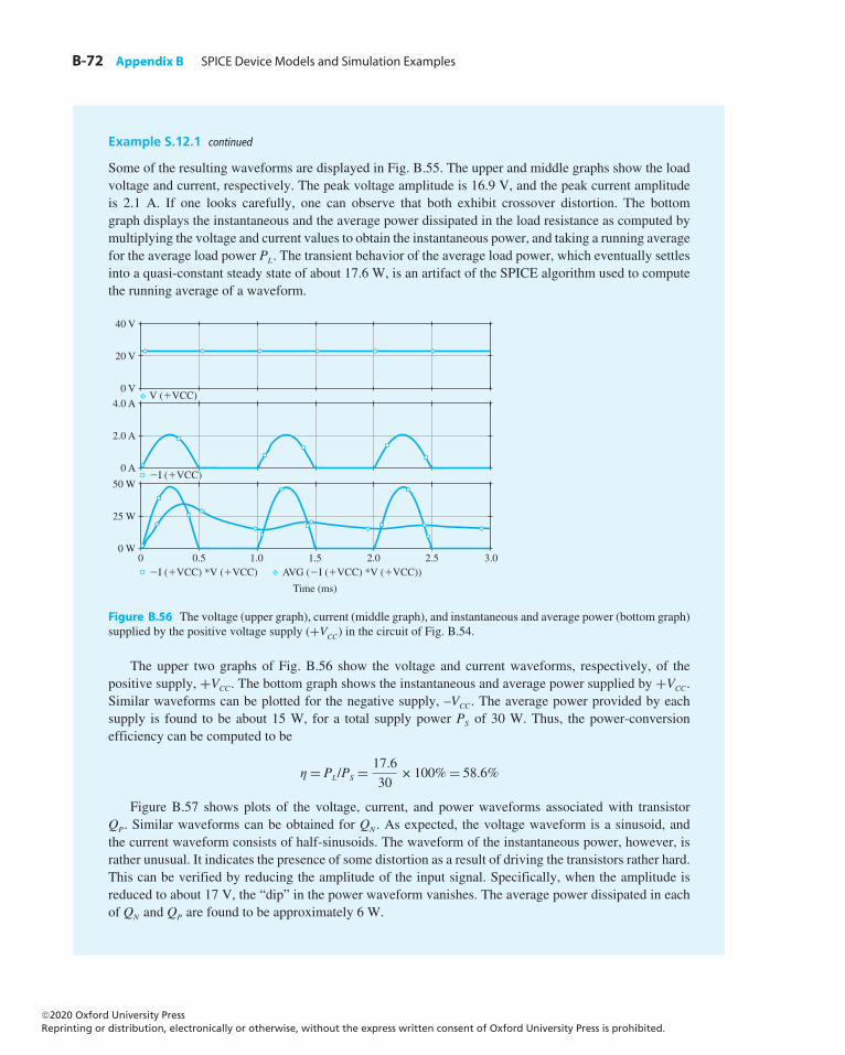
B-72 Appendix B SPICE Device Models and Simulation Examples
Example S.12.1 continued
Some of the resulting waveforms are displayed in Fig. B.55. The upper and middle graphs show the loadvoltage and current, respectively. The peak voltage amplitude is 16.9 V, and the peak current amplitudeis 2.1 A. If one looks carefully, one can observe that both exhibit crossover distortion. The bottomgraph displays the instantaneous and the average power dissipated in the load resistance as computed bymultiplying the voltage and current values to obtain the instantaneous power, and taking a running averagefor the average load power PL. The transient behavior of the average load power, which eventually settlesinto a quasi-constant steady state of about 17.6 W, is an artifact of the SPICE algorithm used to computethe running average of a waveform.
0 V
20 V
40 V
0 0.5 1.0 1.5
Time (ms)
2.0 2.5 3.0
0 A
2.0 A
4.0 A
0 W
25 W
50 W
AVG (�I (�VCC) *V (�VCC))
V (�VCC)
�I (�VCC)
�I (�VCC) *V (�VCC)
Figure B.56 The voltage (upper graph), current (middle graph), and instantaneous and average power (bottom graph)supplied by the positive voltage supply (+VCC) in the circuit of Fig. B.54.
The upper two graphs of Fig. B.56 show the voltage and current waveforms, respectively, of thepositive supply, +VCC. The bottom graph shows the instantaneous and average power supplied by +VCC.Similar waveforms can be plotted for the negative supply, –VCC. The average power provided by eachsupply is found to be about 15 W, for a total supply power PS of 30 W. Thus, the power-conversionefficiency can be computed to be
η = PL/PS = 17.6
30× 100% = 58.6%
Figure B.57 shows plots of the voltage, current, and power waveforms associated with transistorQP. Similar waveforms can be obtained for QN . As expected, the voltage waveform is a sinusoid, andthe current waveform consists of half-sinusoids. The waveform of the instantaneous power, however, israther unusual. It indicates the presence of some distortion as a result of driving the transistors rather hard.This can be verified by reducing the amplitude of the input signal. Specifically, when the amplitude isreduced to about 17 V, the “dip” in the power waveform vanishes. The average power dissipated in eachof QN and QP are found to be approximately 6 W.
©20 Oxford University PressReprinting or distribution, electronically or otherwise, without the express written consent of Oxford University Press is prohibited.
20
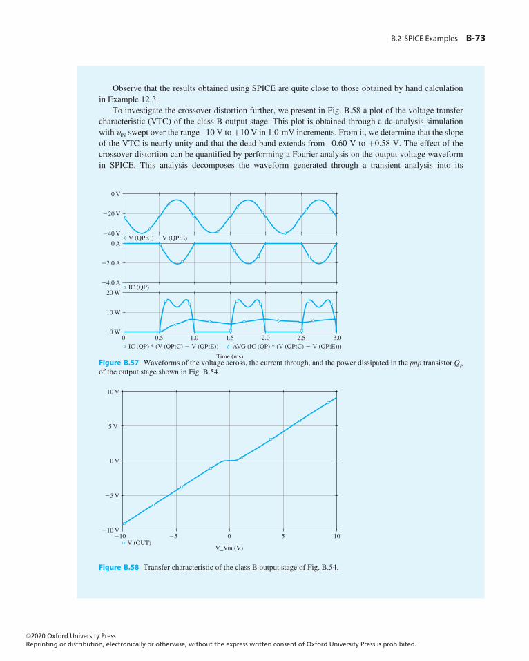
B.2 SPICE Examples B-73
Observe that the results obtained using SPICE are quite close to those obtained by hand calculationin Example 12.3.
To investigate the crossover distortion further, we present in Fig. B.58 a plot of the voltage transfercharacteristic (VTC) of the class B output stage. This plot is obtained through a dc-analysis simulationwith vIN swept over the range –10 V to +10 V in 1.0-mV increments. From it, we determine that the slopeof the VTC is nearly unity and that the dead band extends from –0.60 V to +0.58 V. The effect of thecrossover distortion can be quantified by performing a Fourier analysis on the output voltage waveformin SPICE. This analysis decomposes the waveform generated through a transient analysis into its
�40 V
�20 V
0 V
0 0.5 1.0 1.5
Time (ms)
2.0 2.5 3.0
�4.0 A
�2.0 A
0 A
0 W
10 W
20 W
AVG (IC (QP) * (V (QP:C) � V (QP:E)))
V (QP:C) � V (QP:E)
IC (QP)
IC (QP) * (V (QP:C) � V (QP:E))
Figure B.57 Waveforms of the voltage across, the current through, and the power dissipated in the pnp transistor QP
of the output stage shown in Fig. B.54.
�10 �5V (OUT)
V_Vin (V)
0 5 10�10 V
5 V
0 V
�5 V
10 V
Figure B.58 Transfer characteristic of the class B output stage of Fig. B.54.
©20 Oxford University PressReprinting or distribution, electronically or otherwise, without the express written consent of Oxford University Press is prohibited.
20
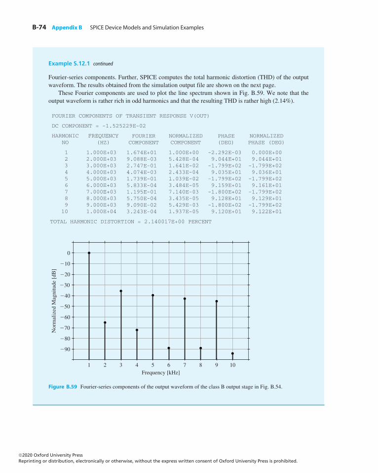
B-74 Appendix B SPICE Device Models and Simulation Examples
Example S.12.1 continued
Fourier-series components. Further, SPICE computes the total harmonic distortion (THD) of the outputwaveform. The results obtained from the simulation output file are shown on the next page.
These Fourier components are used to plot the line spectrum shown in Fig. B.59. We note that theoutput waveform is rather rich in odd harmonics and that the resulting THD is rather high (2.14%).
FOURIER COMPONENTS OF TRANSIENT RESPONSE V(OUT)
HARMONICNO
123456789
10
FREQUENCY(HZ)
1.000E+032.000E+033.000E+034.000E+035.000E+036.000E+037.000E+038.000E+039.000E+031.000E+04
NORMALIZEDCOMPONENT
1.000E+005.428E-041.641E-022.433E-041.039E-023.484E-057.140E-033.435E-055.429E-031.937E-05
NORMALIZEDPHASE (DEG)
0.000E+009.044E+01-1.799E+029.036E+01-1.799E+029.161E+01-1.799E+029.129E+01-1.799E+029.122E+01
TOTAL HARMONIC DISTORTION = 2.140017E+00 PERCENT
-2.292E-039.044E+01-1.799E+029.035E+01-1.799E+029.159E+01-1.800E+029.128E+01-1.800E+029.120E+01
PHASE(DEG)
FOURIERCOMPONENT
1.674E+019.088E-032.747E-014.074E-031.739E-015.833E-041.195E-015.750E-049.090E-023.243E-04
DC COMPONENT = -1.525229E-02
1 2 3 4 5 6 7 8 9 10
�90
�80
�70
�60
�50
�40
�30
�20
0
�10
Frequency [kHz]
Nor
mal
ized
Mag
nitu
de [
dB]
Figure B.59 Fourier-series components of the output waveform of the class B output stage in Fig. B.54.
©20 Oxford University PressReprinting or distribution, electronically or otherwise, without the express written consent of Oxford University Press is prohibited.
20
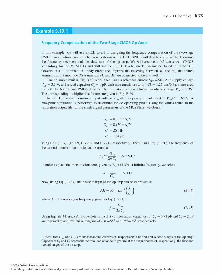
B.2 SPICE Examples B-75
Example S.13.1
Frequency Compensation of the Two-Stage CMOS Op Amp
In this example, we will use SPICE to aid in designing the frequency compensation of the two-stageCMOS circuit whose capture schematic is shown in Fig. B.60. SPICE will then be employed to determinethe frequency response and the slew rate of the op amp. We will assume a 0.5-µm n-well CMOStechnology for the MOSFETs and will use the SPICE level-1 model parameters listed in Table B.3.Observe that to eliminate the body effect and improve the matching between M1 and M2, the sourceterminals of the input PMOS transistorsM1 and M2 are connected to their n well.
The op-amp circuit in Fig. B.60 is designed using a reference current IREF = 90µA, a supply voltageVDD = 3.3 V, and a load capacitor CL = 1 pF. Unit-size transistors with W/L= 1.25 µm/0.6 µm are usedfor both the NMOS and PMOS devices. The transistors are sized for an overdrive voltage VOV = 0.3V.The corresponding multiplicative factors are given in Fig. B.60.
In SPICE, the common-mode input voltage VCM of the op-amp circuit is set to VDD/2=1.65 V. Abias-point simulation is performed to determine the dc operating point. Using the values found in thesimulation output file for the small-signal parameters of the MOSFETs, we obtain14
Gm1 = 0.333mA/V
Gm2 = 0.650mA/V
C1 = 26.5fF
C2 = 1.04pF
using Eqs. (13.7), (13.12), (13.20), and (13.21), respectively. Then, using Eq. (13.30), the frequency ofthe second, nondominant, pole can be found as
fP2 � Gm2
2πC2
= 97.2MHz
In order to place the transmission zero, given by Eq. (13.39), at infinite frequency, we select
R= 1
Gm2
= 1.53k�
Now, using Eq. (13.37), the phase margin of the op amp can be expressed as
PM = 90°−tan−1
(ftfP2
)(B.44)
where ft is the unity-gain frequency, given in Eq. (13.31),
ft =Gm1
2πCC
(B.45)
Using Eqs. (B.44) and (B.45), we determine that compensation capacitors of CC = 0.78 pF and CC = 2 pFare required to achieve phase margins of PM=55° and PM=75°, respectively.
14Recall that Gm1 and Gm2 are the transconductances of, respectively, the first and second stages of the op amp.Capacitors C1 and C2 represent the total capacitance to ground at the output nodes of, respectively, the first andsecond stages of the op amp.
©20 Oxford University PressReprinting or distribution, electronically or otherwise, without the express written consent of Oxford University Press is prohibited.
20
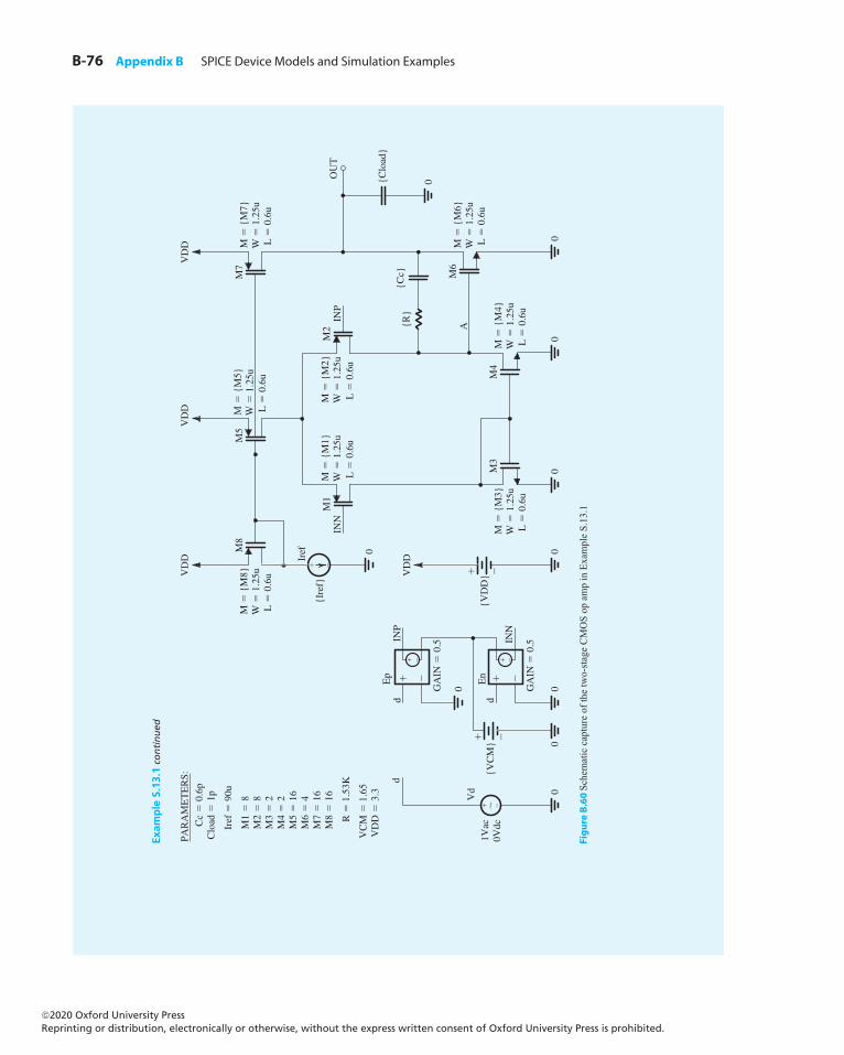
B-76 Appendix B SPICE Device Models and Simulation Examples
INN
d {V
CM
}
GA
IN
0.5
1Vac
0V
dc
Vd 0
d
0 0
INP
INN
En
INP
d
GA
IN
0.5
0
Ep
{VD
D}
M
{M
3}
W
1.2
5u
L
0.6
u
M
{M
4}
W
1.2
5u
L
0.6
u
M
{M
6}
W
1.2
5u
L
0.6
u
M
{M
8}
W
1.2
5u
L
0.6
u
M
{M
1}
W
1.2
5u
L
0.6
u
{Cc}
{R
}
{Clo
ad}
OU
T
M
{M
2}
W
1.2
5u
L
0.6
u
VD
D
M3
M1
M8
M5
M2
M4
A
0
VD
D 0
0
{Ire
f}
Iref
0
M6
0
0
VD
D
M7
VD
D
M
{M
5}
W
1.2
5u
L
0.6
u
M
{M
7}
W
1.2
5u
L
0.6
u
Cc
0
.6p
Clo
ad
1p
Iref
9
0u
M1
8
M
2
8
M3
2
M
4
2
M5
1
6 M
6
4
M7
1
6 M
8
16
R
1.5
3K
VC
M
1.6
5 V
DD
3.
3
PAR
AM
ET
ER
S:
Fig
ure
B.6
0 S
chem
atic
cap
ture
of t
he tw
o-st
age
CM
OS
op a
mp
in E
xam
ple
S.13
.1
Exa m
ple
S.1
3.1 continued
©20 Oxford University PressReprinting or distribution, electronically or otherwise, without the express written consent of Oxford University Press is prohibited.
20
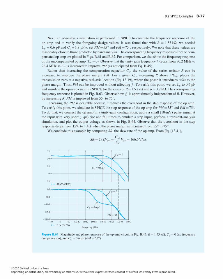
B.2 SPICE Examples B-77
Next, an ac-analysis simulation is performed in SPICE to compute the frequency response of theop amp and to verify the foregoing design values. It was found that with R = 1.53 k�, we neededCC = 0.6 pF and CC =1.8 pF to set PM=55° and PM=75°, respectively. We note that these values arereasonably close to those predicted by hand analysis. The corresponding frequency responses for the com-pensated op amp are plotted in Figs. B.61 and B.62. For comparison, we also show the frequency responseof the uncompensated op amp (CC =0). Observe that the unity gain frequency ft drops from 70.2 MHz to26.4 MHz as CC is increased to improve PM (as anticipated from Eq. B.45).
Rather than increasing the compensation capacitor CC, the value of the series resistor R can beincreased to improve the phase margin PM: For a given CC, increasing R above 1/Gm2 places thetransmission zero at a negative real-axis location (Eq. 13.39), where the phase it introduces adds to thephase margin. Thus, PM can be improved without affecting ft. To verify this point, we set CC to 0.6 pFand simulate the op-amp circuit in SPICE for the cases of R=1.53 k� and R=3.2 k�. The correspondingfrequency response is plotted in Fig. B.63. Observe how ft is approximately independent of R. However,by increasing R, PM is improved from 55° to 75°.
Increasing the PM is desirable because it reduces the overshoot in the step response of the op amp.To verify this point, we simulate in SPICE the step response of the op amp for PM=55° and PM=75°.To do that, we connect the op amp in a unity-gain configuration, apply a small (10-mV) pulse signal atthe input with very short (1-ps) rise and fall times to emulate a step input, perform a transient-analysissimulation, and plot the output voltage as shown in Fig. B.64. Observe that the overshoot in the stepresponse drops from 15% to 1.4% when the phase margin is increased from 55° to 75°.
We conclude this example by computing SR, the slew rate of the op amp. From Eq. (13.41),
SR= 2π ftVOV = Gm1
CC
VOV = 166.5V/µs
�25
25
50
0
75
�180d
�90d
�45d
�135d
0d
Frequency (Hz)
1.0 10 100 1.0 K 10 K 100 K 1.0 M 10 M 100 M 1.0 G
dB (V (OUT))
CC � 0.6 pF
CC � 0
CC � 0
CC � 0.6 pF
PM � 55
P (V (OUT))
Figure B.61 Magnitude and phase response of the op-amp circuit in Fig. B.43: R= 1.53 k�, CC = 0 (no frequencycompensation), and CC = 0.6 pF (PM = 55°).
©20 Oxford University PressReprinting or distribution, electronically or otherwise, without the express written consent of Oxford University Press is prohibited.
20
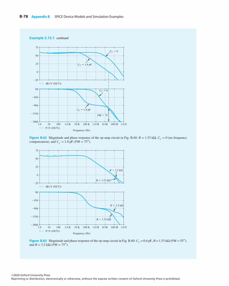
B-78 Appendix B SPICE Device Models and Simulation Examples
Example S.13.1 continued
�25
25
50
0
75
�180d
�90d
�45d
�135d
0d
Frequency (Hz)
1.0 10 100 1.0 K 10 K 100 K 1.0 M 10 M 100 M 1.0 G
dB (V (OUT))
CC � 1.8 pF
CC � 0
CC � 1.8 pF
P (V (OUT))
PM � 75
CC � 0
Figure B.62 Magnitude and phase response of the op-amp circuit in Fig. B.60: R= 1.53 k�, CC = 0 (no frequencycompensation), and CC = 1.8 pF (PM = 75°).
�25
25
50
0
75
�180d
�90d
�45d
�135d
0d
Frequency (Hz)
1.0 10 100 1.0 K 10 K 100 K 1.0 M 10 M 100 M 1.0 G
dB (V (OUT))
R � 1.53 kΩ
R � 3.2 kΩ
R � 3.2 kΩ
R � 1.53 kΩ
P (V (OUT))
Figure B.63 Magnitude and phase response of the op-amp circuit in Fig. B.60: CC =0.6 pF, R=1.53 k� (PM= 55°),and R= 3.2 k� (PM = 75°).
©20 Oxford University PressReprinting or distribution, electronically or otherwise, without the express written consent of Oxford University Press is prohibited.
20
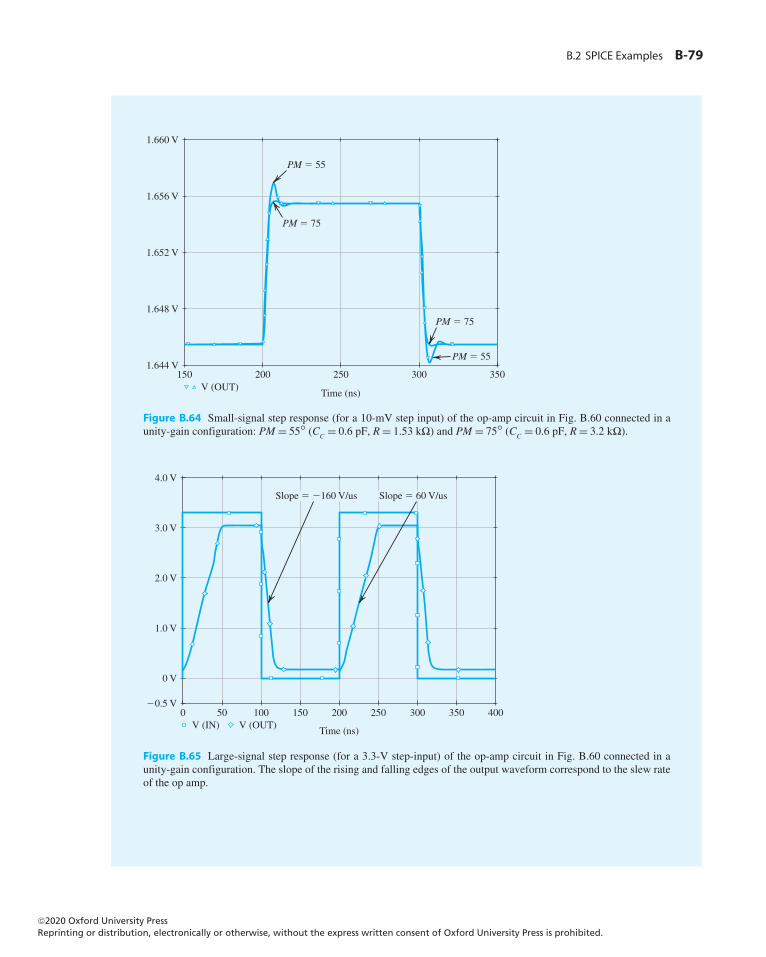
B.2 SPICE Examples B-79
V (OUT)
1.660 V
150 200 250 300 350 1.644 V
1.648 V
1.652 V
1.656 V
Time (ns)
PM � 55
PM � 75
PM � 75
PM � 55
Figure B.64 Small-signal step response (for a 10-mV step input) of the op-amp circuit in Fig. B.60 connected in aunity-gain configuration: PM = 55° (CC = 0.6 pF, R= 1.53 k�) and PM = 75° (CC = 0.6 pF, R= 3.2 k�).
Time (ns)
Slope � �160 V/us Slope � 60 V/us
0 50 100 150 200 250 300 350 400
0 V
1.0 V
2.0 V
3.0 V
4.0 V
�0.5 V
V (IN) V (OUT)
Figure B.65 Large-signal step response (for a 3.3-V step-input) of the op-amp circuit in Fig. B.60 connected in aunity-gain configuration. The slope of the rising and falling edges of the output waveform correspond to the slew rateof the op amp.
©20 Oxford University PressReprinting or distribution, electronically or otherwise, without the express written consent of Oxford University Press is prohibited.
20
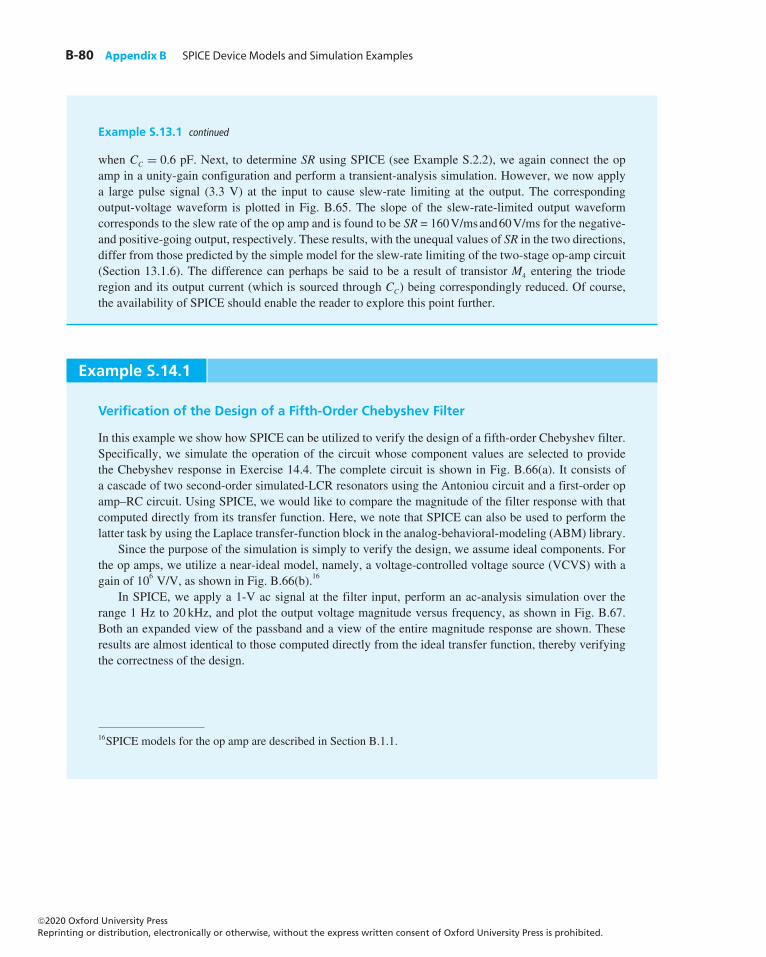
B-80 Appendix B SPICE Device Models and Simulation Examples
Example S.13.1 continued
when CC = 0.6 pF. Next, to determine SR using SPICE (see Example S.2.2), we again connect the opamp in a unity-gain configuration and perform a transient-analysis simulation. However, we now applya large pulse signal (3.3 V) at the input to cause slew-rate limiting at the output. The correspondingoutput-voltage waveform is plotted in Fig. B.65. The slope of the slew-rate-limited output waveformcorresponds to the slew rate of the op amp and is found to be SR = 160V/msand60V/ms for the negative-and positive-going output, respectively. These results, with the unequal values of SR in the two directions,differ from those predicted by the simple model for the slew-rate limiting of the two-stage op-amp circuit(Section 13.1.6). The difference can perhaps be said to be a result of transistor M4 entering the trioderegion and its output current (which is sourced through CC) being correspondingly reduced. Of course,the availability of SPICE should enable the reader to explore this point further.
Example S.14.1
Verification of the Design of a Fifth-Order Chebyshev Filter
In this example we show how SPICE can be utilized to verify the design of a fifth-order Chebyshev filter.Specifically, we simulate the operation of the circuit whose component values are selected to providethe Chebyshev response in Exercise 14.4. The complete circuit is shown in Fig. B.66(a). It consists ofa cascade of two second-order simulated-LCR resonators using the Antoniou circuit and a first-order opamp–RC circuit. Using SPICE, we would like to compare the magnitude of the filter response with thatcomputed directly from its transfer function. Here, we note that SPICE can also be used to perform thelatter task by using the Laplace transfer-function block in the analog-behavioral-modeling (ABM) library.
Since the purpose of the simulation is simply to verify the design, we assume ideal components. Forthe op amps, we utilize a near-ideal model, namely, a voltage-controlled voltage source (VCVS) with again of 106 V/V, as shown in Fig. B.66(b).16
In SPICE, we apply a 1-V ac signal at the filter input, perform an ac-analysis simulation over therange 1 Hz to 20 kHz, and plot the output voltage magnitude versus frequency, as shown in Fig. B.67.Both an expanded view of the passband and a view of the entire magnitude response are shown. Theseresults are almost identical to those computed directly from the ideal transfer function, thereby verifyingthe correctness of the design.
16SPICE models for the op amp are described in Section B.1.1.
©20 Oxford University PressReprinting or distribution, electronically or otherwise, without the express written consent of Oxford University Press is prohibited.
20
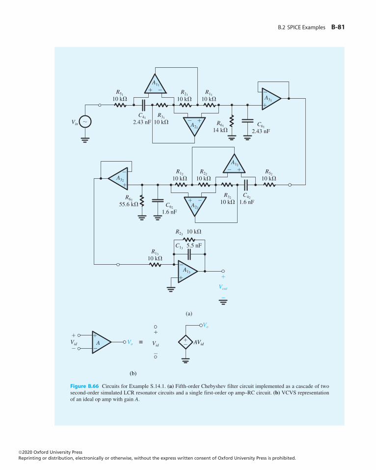
B.2 SPICE Examples B-81
�
�
VidVo
Vo
Vid A
�
�
�
�
�� AVid
(b)
Figure B.66 Circuits for Example S.14.1. (a) Fifth-order Chebyshev filter circuit implemented as a cascade of twosecond-order simulated LCR resonator circuits and a single first-order op amp–RC circuit. (b) VCVS representationof an ideal op amp with gain A.
©20 Oxford University PressReprinting or distribution, electronically or otherwise, without the express written consent of Oxford University Press is prohibited.
20
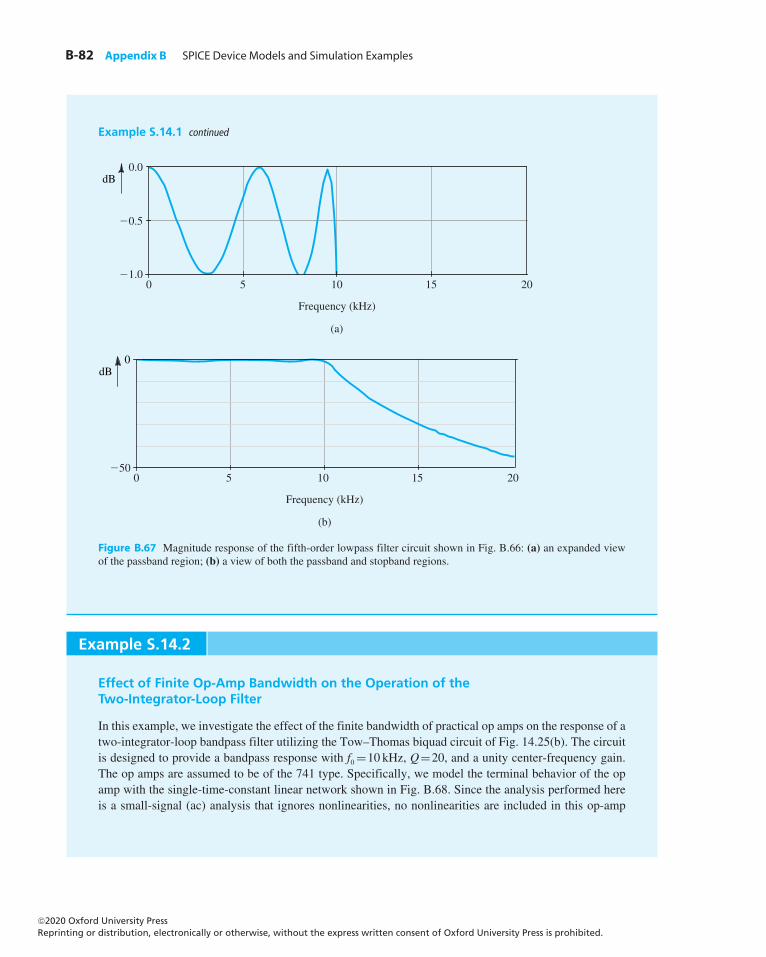
B-82 Appendix B SPICE Device Models and Simulation Examples
Example S.14.1 continued
�0.5
�1.0
0.0dB
0 5
Frequency (kHz)
10 15 20
(a)
0 5
Frequency (kHz)
10 15 20 �50
0dB
(b)
Figure B.67 Magnitude response of the fifth-order lowpass filter circuit shown in Fig. B.66: (a) an expanded viewof the passband region; (b) a view of both the passband and stopband regions.
Example S.14.2
Effect of Finite Op-Amp Bandwidth on the Operation of theTwo-Integrator-Loop Filter
In this example, we investigate the effect of the finite bandwidth of practical op amps on the response of atwo-integrator-loop bandpass filter utilizing the Tow–Thomas biquad circuit of Fig. 14.25(b). The circuitis designed to provide a bandpass response with f0 =10 kHz, Q=20, and a unity center-frequency gain.The op amps are assumed to be of the 741 type. Specifically, we model the terminal behavior of the opamp with the single-time-constant linear network shown in Fig. B.68. Since the analysis performed hereis a small-signal (ac) analysis that ignores nonlinearities, no nonlinearities are included in this op-amp
©20 Oxford University PressReprinting or distribution, electronically or otherwise, without the express written consent of Oxford University Press is prohibited.
20
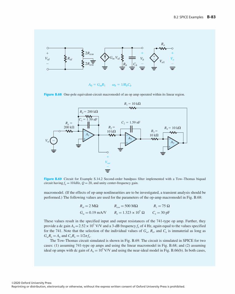
B.2 SPICE Examples B-83
A0 � GmR1 b � 1/RbCb
Gm Vid
�
�
Vb
�
�
Vid
Rb Cb
Ro
Vo1�
�
VoRid
2Ricm
2Ricm
��
Figure B.68 One-pole equivalent-circuit macromodel of an op amp operated within its linear region.
�
�
Rg �200 k�
A1 �
�
A2 �
�
A3
Vout
�
�
C1 � 1.59 nF
C2 � 1.59 nF
Rd � 200 k�
R2 �
10 k� R3 �
10 k�
R4 � 10 k�
Vin
R1 � 10 k�
Figure B.69 Circuit for Example S.14.2 Second-order bandpass filter implemented with a Tow–Thomas biquadcircuit having f0 = 10 kHz, Q= 20, and unity center-frequency gain.
macromodel. (If the effects of op-amp nonlinearities are to be investigated, a transient analysis should beperformed.) The following values are used for the parameters of the op-amp macromodel in Fig. B.68:
Rid = 2 M� Ricm = 500 M� R1 = 75 �
Gm = 0.19 mA/V Rb = 1.323× 10⁹� Cb = 30 pF
These values result in the specified input and output resistances of the 741-type op amp. Further, theyprovide a dc gain A0 =2.52×10⁵ V/V and a 3-dB frequency fb of 4 Hz, again equal to the values specifiedfor the 741. Note that the selection of the individual values of Gm, Rb, and Cb is immaterial as long asGmRb = A0 and CbRb = 1/2π fb.
The Tow-Thomas circuit simulated is shown in Fig. B.69. The circuit is simulated in SPICE for twocases: (1) assuming 741-type op amps and using the linear macromodel in Fig. B.68; and (2) assumingideal op amps with dc gain of A0 = 106V/V and using the near-ideal model in Fig. B.66(b). In both cases,
©20 Oxford University PressReprinting or distribution, electronically or otherwise, without the express written consent of Oxford University Press is prohibited.
20
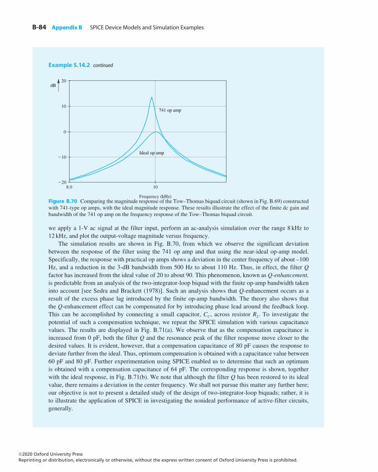
B-84 Appendix B SPICE Device Models and Simulation Examples
Example S.14.2 continued
�20
10
0
�10
20dB
8.0
Frequency (kHz)
10
741 op amp
Ideal op amp
Figure B.70 Comparing the magnitude response of the Tow–Thomas biquad circuit (shown in Fig. B.69) constructedwith 741-type op amps, with the ideal magnitude response. These results illustrate the effect of the finite dc gain andbandwidth of the 741 op amp on the frequency response of the Tow–Thomas biquad circuit.
we apply a 1-V ac signal at the filter input, perform an ac-analysis simulation over the range 8 kHz to12 kHz, and plot the output-voltage magnitude versus frequency.
The simulation results are shown in Fig. B.70, from which we observe the significant deviationbetween the response of the filter using the 741 op amp and that using the near-ideal op-amp model.Specifically, the response with practical op amps shows a deviation in the center frequency of about –100Hz, and a reduction in the 3-dB bandwidth from 500 Hz to about 110 Hz. Thus, in effect, the filter Qfactor has increased from the ideal value of 20 to about 90. This phenomenon, known as Q-enhancement,is predictable from an analysis of the two-integrator-loop biquad with the finite op-amp bandwidth takeninto account [see Sedra and Brackett (1978)]. Such an analysis shows that Q-enhancement occurs as aresult of the excess phase lag introduced by the finite op-amp bandwidth. The theory also shows thatthe Q-enhancement effect can be compensated for by introducing phase lead around the feedback loop.This can be accomplished by connecting a small capacitor, CC, across resistor R2. To investigate thepotential of such a compensation technique, we repeat the SPICE simulation with various capacitancevalues. The results are displayed in Fig. B.71(a). We observe that as the compensation capacitance isincreased from 0 pF, both the filter Q and the resonance peak of the filter response move closer to thedesired values. It is evident, however, that a compensation capacitance of 80 pF causes the response todeviate further from the ideal. Thus, optimum compensation is obtained with a capacitance value between60 pF and 80 pF. Further experimentation using SPICE enabled us to determine that such an optimumis obtained with a compensation capacitance of 64 pF. The corresponding response is shown, togetherwith the ideal response, in Fig. B.71(b). We note that although the filter Q has been restored to its idealvalue, there remains a deviation in the center frequency. We shall not pursue this matter any further here;our objective is not to present a detailed study of the design of two-integrator-loop biquads; rather, it isto illustrate the application of SPICE in investigating the nonideal performance of active-filter circuits,generally.
©20 Oxford University PressReprinting or distribution, electronically or otherwise, without the express written consent of Oxford University Press is prohibited.
20
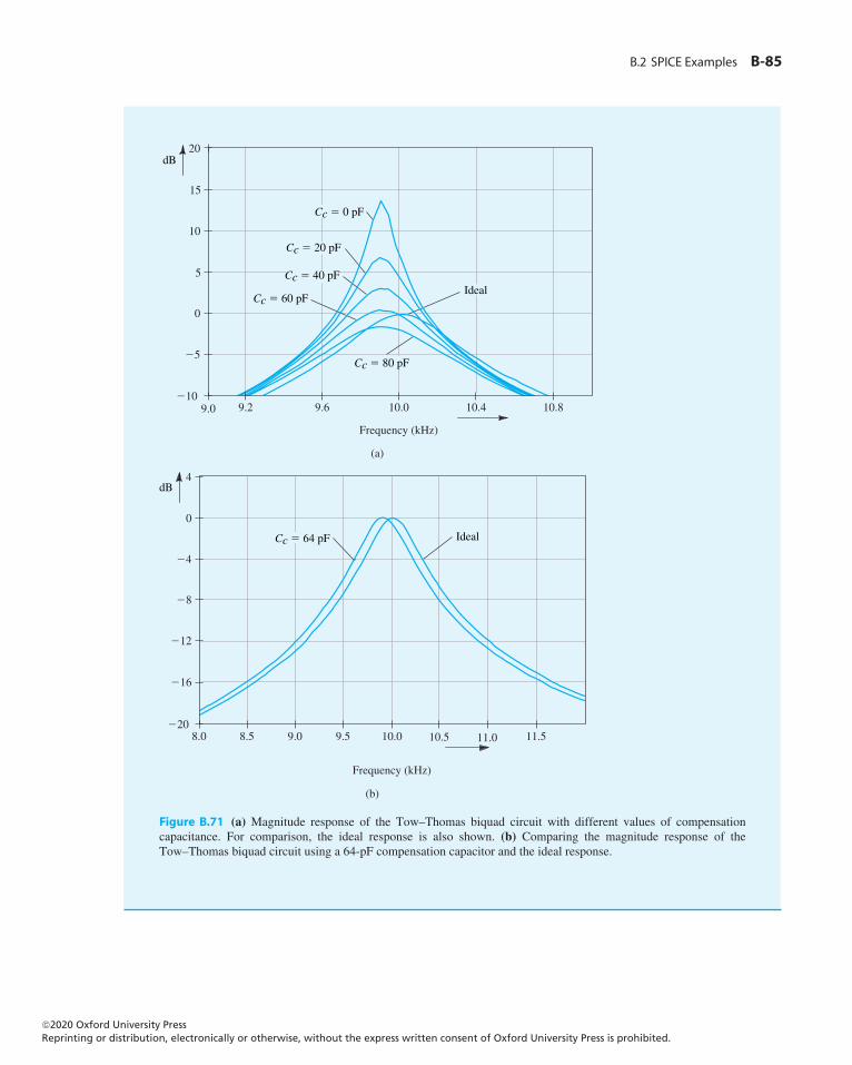
B.2 SPICE Examples B-85
(a)
�10
15
5
�5
20
0
dB
10
Cc � 60 pF
Cc � 20 pF
Cc � 0 pF
Cc � 80 pF
Cc � 40 pFIdeal
9.0 9.2 10.0 10.49.6 10.8
Frequency (kHz)
(b)
8.0 8.5 10.0 11.010.59.59.0 11.5
Frequency (kHz)
�20
0
�8
�16
4
�12
�4
dB
Cc � 64 pF Ideal
Figure B.71 (a) Magnitude response of the Tow–Thomas biquad circuit with different values of compensationcapacitance. For comparison, the ideal response is also shown. (b) Comparing the magnitude response of theTow–Thomas biquad circuit using a 64-pF compensation capacitor and the ideal response.
©20 Oxford University PressReprinting or distribution, electronically or otherwise, without the express written consent of Oxford University Press is prohibited.
20
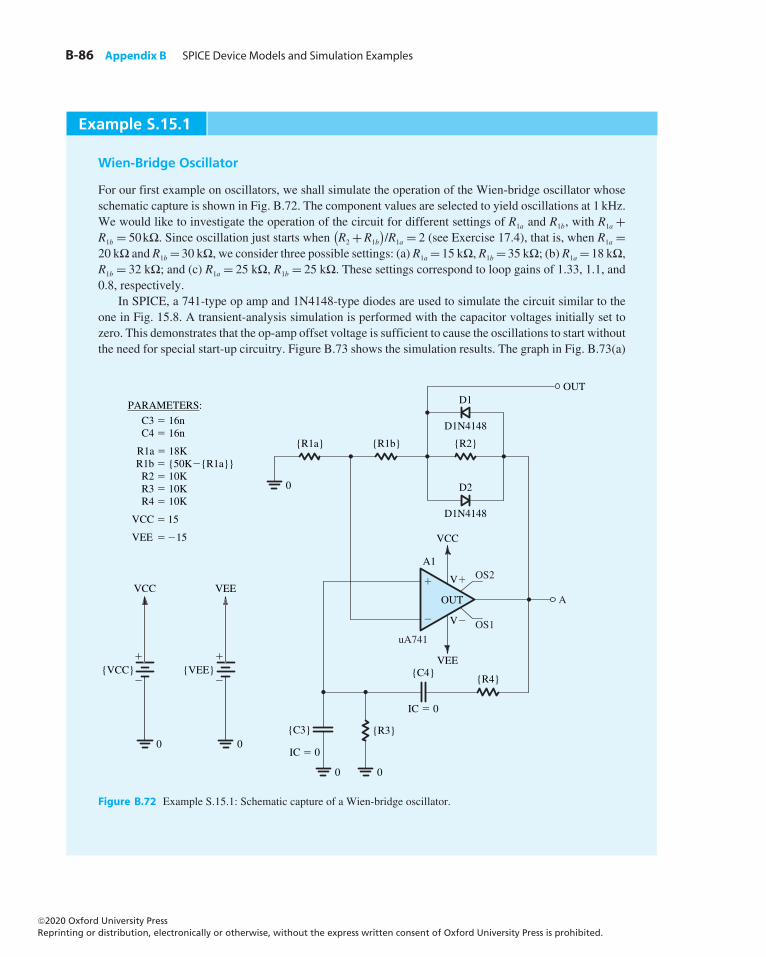
B-86 Appendix B SPICE Device Models and Simulation Examples
Example S.15.1
Wien-Bridge Oscillator
For our first example on oscillators, we shall simulate the operation of the Wien-bridge oscillator whoseschematic capture is shown in Fig. B.72. The component values are selected to yield oscillations at 1 kHz.We would like to investigate the operation of the circuit for different settings of R1a and R1b, with R1a +R1b = 50k�. Since oscillation just starts when
(R2 +R1b
)/R1a = 2 (see Exercise 17.4), that is, when R1a =
20 k� and R1b = 30 k�, we consider three possible settings: (a) R1a = 15 k�, R1b = 35 k�; (b) R1a = 18 k�,R1b = 32 k�; and (c) R1a = 25 k�, R1b = 25 k�. These settings correspond to loop gains of 1.33, 1.1, and0.8, respectively.
In SPICE, a 741-type op amp and 1N4148-type diodes are used to simulate the circuit similar to theone in Fig. 15.8. A transient-analysis simulation is performed with the capacitor voltages initially set tozero. This demonstrates that the op-amp offset voltage is sufficient to cause the oscillations to start withoutthe need for special start-up circuitry. Figure B.73 shows the simulation results. The graph in Fig. B.73(a)
{VEE}
VEE
�
�
0
{VCC}
VCC
�
�
0
C3 � 16n C4 � 16n
R1a � 18K R1b � {50K�{R1a}} R2 � 10K R3 � 10K R4 � 10K
VCC � 15
VEE � �15
PARAMETERS:
{R2}
{R3}
0
{C3}
{R4}{C4}
IC � 0
IC � 0
0 0
{R1b}
D2
D1OUT
D1N4148
D1N4148
{R1a}
VEE
VCC
A1
V�
V�
OS2
A
OS1uA741
OUT
�
�
Figure B.72 Example S.15.1: Schematic capture of a Wien-bridge oscillator.
©20 Oxford University PressReprinting or distribution, electronically or otherwise, without the express written consent of Oxford University Press is prohibited.
20
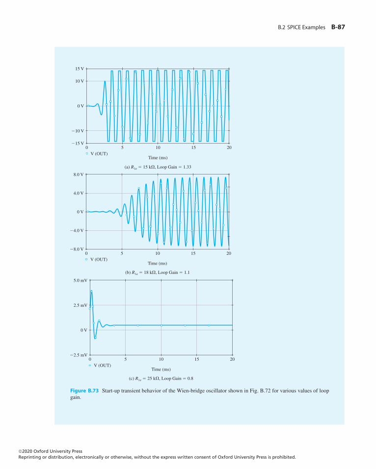
B.2 SPICE Examples B-87
Figure B.73 Start-up transient behavior of the Wien-bridge oscillator shown in Fig. B.72 for various values of loopgain.
©20 Oxford University PressReprinting or distribution, electronically or otherwise, without the express written consent of Oxford University Press is prohibited.
20
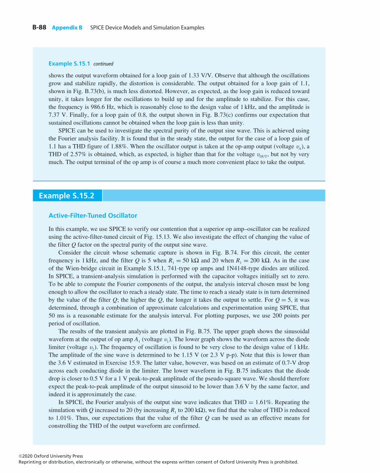
B-88 Appendix B SPICE Device Models and Simulation Examples
Example S.15.1 continued
shows the output waveform obtained for a loop gain of 1.33 V/V. Observe that although the oscillationsgrow and stabilize rapidly, the distortion is considerable. The output obtained for a loop gain of 1.1,shown in Fig. B.73(b), is much less distorted. However, as expected, as the loop gain is reduced towardunity, it takes longer for the oscillations to build up and for the amplitude to stabilize. For this case,the frequency is 986.6 Hz, which is reasonably close to the design value of 1 kHz, and the amplitude is7.37 V. Finally, for a loop gain of 0.8, the output shown in Fig. B.73(c) confirms our expectation thatsustained oscillations cannot be obtained when the loop gain is less than unity.
SPICE can be used to investigate the spectral purity of the output sine wave. This is achieved usingthe Fourier analysis facility. It is found that in the steady state, the output for the case of a loop gain of1.1 has a THD figure of 1.88%. When the oscillator output is taken at the op-amp output (voltage vA), aTHD of 2.57% is obtained, which, as expected, is higher than that for the voltage vOUT, but not by verymuch. The output terminal of the op amp is of course a much more convenient place to take the output.
Example S.15.2
Active-Filter-Tuned Oscillator
In this example, we use SPICE to verify our contention that a superior op amp–oscillator can be realizedusing the active-filter-tuned circuit of Fig. 15.13. We also investigate the effect of changing the value ofthe filter Q factor on the spectral purity of the output sine wave.
Consider the circuit whose schematic capture is shown in Fig. B.74. For this circuit, the centerfrequency is 1 kHz, and the filter Q is 5 when R1 = 50 k� and 20 when R1 = 200 k�. As in the caseof the Wien-bridge circuit in Example S.15.1, 741-type op amps and 1N4148-type diodes are utilized.In SPICE, a transient-analysis simulation is performed with the capacitor voltages initially set to zero.To be able to compute the Fourier components of the output, the analysis interval chosen must be longenough to allow the oscillator to reach a steady state. The time to reach a steady state is in turn determinedby the value of the filter Q; the higher the Q, the longer it takes the output to settle. For Q = 5, it wasdetermined, through a combination of approximate calculations and experimentation using SPICE, that50 ms is a reasonable estimate for the analysis interval. For plotting purposes, we use 200 points perperiod of oscillation.
The results of the transient analysis are plotted in Fig. B.75. The upper graph shows the sinusoidalwaveform at the output of op amp A1 (voltage v1). The lower graph shows the waveform across the diodelimiter (voltage v2). The frequency of oscillation is found to be very close to the design value of 1 kHz.The amplitude of the sine wave is determined to be 1.15 V (or 2.3 V p-p). Note that this is lower thanthe 3.6 V estimated in Exercise 15.9. The latter value, however, was based on an estimate of 0.7-V dropacross each conducting diode in the limiter. The lower waveform in Fig. B.75 indicates that the diodedrop is closer to 0.5 V for a 1 V peak-to-peak amplitude of the pseudo-square wave. We should thereforeexpect the peak-to-peak amplitude of the output sinusoid to be lower than 3.6 V by the same factor, andindeed it is approximately the case.
In SPICE, the Fourier analysis of the output sine wave indicates that THD = 1.61%. Repeating thesimulation with Q increased to 20 (by increasing R1 to 200 k�), we find that the value of THD is reducedto 1.01%. Thus, our expectations that the value of the filter Q can be used as an effective means forconstrolling the THD of the output waveform are confirmed.
©20 Oxford University PressReprinting or distribution, electronically or otherwise, without the express written consent of Oxford University Press is prohibited.
20
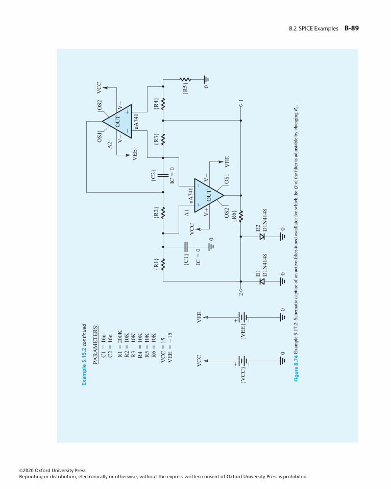
B.2 SPICE Examples B-89
uA74
1V
CC
VE
E
VC
C
VE
E
{C1}
{R6}
2
{R1}
{R2}
{R3}
{R4}
IC
0
IC
0
D1
D1N
4148
D2
D1N
4148
{R5}
{C2}
0
00
0
1
OU
T
OS2
OS1
OS1
A2
uA74
1
A1
OS2
OU
T
{VE
E}V
EE
0
{VC
C}V
CC
0
C
1 1
6n
C2
16n
R
1 2
00K
R
2 1
0K
R3
10K
R
4
10K
R
5 1
0K
R6
10K
VC
C
15
VE
E
15
PAR
AM
ET
ER
S:
VV
VV
Exa
mpl
e S.
17.2
: Sch
emat
ic c
aptu
re o
f an
act
ive-
filte
r-tu
ned
osci
llato
r for
whi
ch th
e Q
of
the
filte
r is
adju
stab
le b
y ch
angi
ng R
1.
Exam
ple
S.1
5.2 continued
Fig
ure
B.7
4
©20 Oxford University PressReprinting or distribution, electronically or otherwise, without the express written consent of Oxford University Press is prohibited.
20
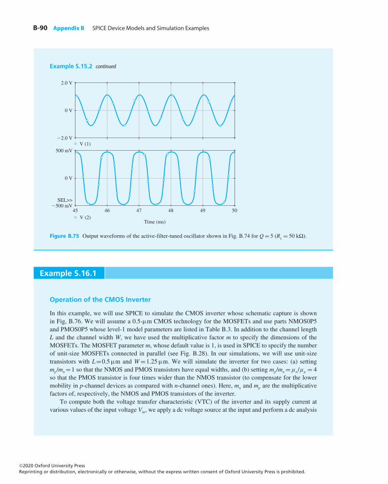
B-90 Appendix B SPICE Device Models and Simulation Examples
Example S.15.2 continued
�2.0 V
0 V
2.0 V
0 V
45 46 47 48
Time (ms)
49 50
500 mV
SEL>>�500 mV
V (1)
V (2)
Figure B.75 Output waveforms of the active-filter-tuned oscillator shown in Fig. B.74 for Q= 5 (R1 = 50 k�).
Example S.16.1
Operation of the CMOS Inverter
In this example, we will use SPICE to simulate the CMOS inverter whose schematic capture is shownin Fig, B.76. We will assume a 0.5-µm CMOS technology for the MOSFETs and use parts NMOS0P5and PMOS0P5 whose level-1 model parameters are listed in Table B.3. In addition to the channel lengthL and the channel width W, we have used the multiplicative factor m to specify the dimensions of theMOSFETs. The MOSFET parameter m, whose default value is 1, is used in SPICE to specify the numberof unit-size MOSFETs connected in parallel (see Fig. B.28). In our simulations, we will use unit-sizetransistors with L=0.5µm and W=1.25µm. We will simulate the inverter for two cases: (a) settingmp/mn=1 so that the NMOS and PMOS transistors have equal widths, and (b) setting mp/mn=μn/μp = 4so that the PMOS transistor is four times wider than the NMOS transistor (to compensate for the lowermobility in p-channel devices as compared with n-channel ones). Here, mn and mp are the multiplicativefactors of, respectively, the NMOS and PMOS transistors of the inverter.
To compute both the voltage transfer characteristic (VTC) of the inverter and its supply current atvarious values of the input voltage Vin, we apply a dc voltage source at the input and perform a dc analysis
©20 Oxford University PressReprinting or distribution, electronically or otherwise, without the express written consent of Oxford University Press is prohibited.
20
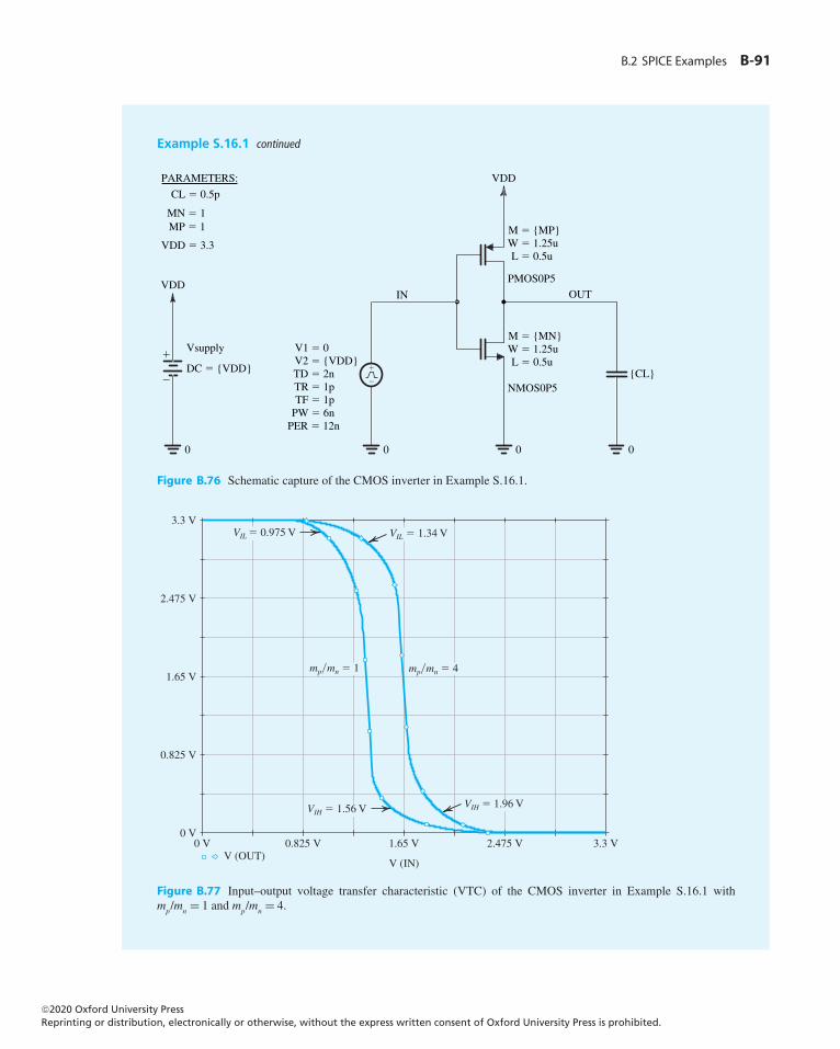
B.2 SPICE Examples B-91
Example S.16.1 continued
V1 � 0 V2 � {VDD} TD � 2n TR � 1p TF � 1p PW � 6nPER � 12n
OUT
M � {MN}W � 1.25u L � 0.5u
NMOS0P5
Vsupply
VDD
DC � {VDD}�
�
VDD
0
{CL}
00
IN
0
M � {MP}W � 1.25u L � 0.5u
PMOS0P5
PARAMETERS:
CL � 0.5p
�
�
MN � 1 MP � 1
VDD � 3.3
Figure B.76 Schematic capture of the CMOS inverter in Example S.16.1.
V (IN)
0 V 0.825 V 1.65 V 2.475 V 3.3 V0 V
0.825 V
1.65 V
2.475 V
3.3 V
V (OUT)
VIH � 1.96 V
mp�mn � 4mp�mn � 1
VIH � 1.56 V
VIL � 1.34 VVIL � 0.975 V
Figure B.77 Input–output voltage transfer characteristic (VTC) of the CMOS inverter in Example S.16.1 withmp/mn = 1 and mp/mn = 4.
©20 Oxford University PressReprinting or distribution, electronically or otherwise, without the express written consent of Oxford University Press is prohibited.
20
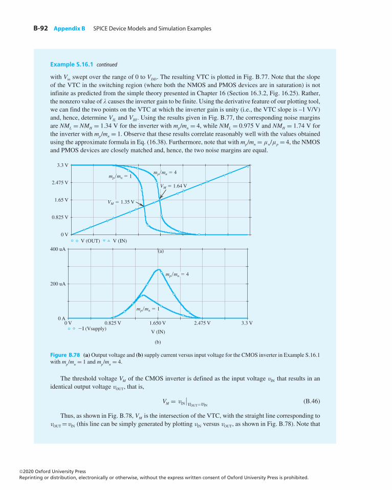
B-92 Appendix B SPICE Device Models and Simulation Examples
Example S.16.1 continued
with Vin swept over the range of 0 to VDD. The resulting VTC is plotted in Fig. B.77. Note that the slopeof the VTC in the switching region (where both the NMOS and PMOS devices are in saturation) is notinfinite as predicted from the simple theory presented in Chapter 16 (Section 16.3.2, Fig. 16.25). Rather,the nonzero value of λ causes the inverter gain to be finite. Using the derivative feature of our plotting tool,we can find the two points on the VTC at which the inverter gain is unity (i.e., the VTC slope is –1 V/V)and, hence, determine VIL and VIH . Using the results given in Fig. B.77, the corresponding noise marginsare NML = NMH = 1.34 V for the inverter with mp/mn = 4, while NML = 0.975 V and NMH = 1.74 V forthe inverter with mp/mn = 1. Observe that these results correlate reasonably well with the values obtainedusing the approximate formula in Eq. (16.38). Furthermore, note that with mp/mn = μn/μp = 4, the NMOSand PMOS devices are closely matched and, hence, the two noise margins are equal.
0 V
1.65 V
2.475 V
0.825 V
3.3 V
V (OUT) V (IN)
(a)
VM � 1.64 V
mp�mn � 4 mp�mn � 1
VM � 1.35 V
V (IN)
(b)
0 V 0.825 V 1.650 V 2.475 V 3.3 V 0 A
200 uA
400 uA
�I (Vsupply)
mp�mn � 4
mp�mn � 1
Figure B.78 (a)Output voltage and (b) supply current versus input voltage for the CMOS inverter in Example S.16.1with mp/mn = 1 and mp/mn = 4.
The threshold voltage VM of the CMOS inverter is defined as the input voltage vIN that results in anidentical output voltage vOUT, that is,
VM = vIN
∣∣vOUT=vIN
(B.46)
Thus, as shown in Fig. B.78, VM is the intersection of the VTC, with the straight line corresponding tovOUT =vIN (this line can be simply generated by plotting vIN versus vOUT, as shown in Fig. B.78). Note that
©20 Oxford University PressReprinting or distribution, electronically or otherwise, without the express written consent of Oxford University Press is prohibited.
20
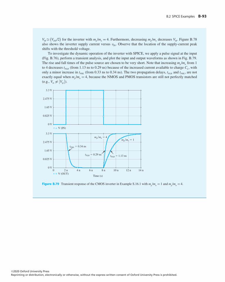
B.2 SPICE Examples B-93
VM �(VDD/2
)for the inverter with mp/mn = 4. Furthermore, decreasing mp/mn decreases VM . Figure B.78
also shows the inverter supply current versus vIN. Observe that the location of the supply-current peakshifts with the threshold voltage.
To investigate the dynamic operation of the inverter with SPICE, we apply a pulse signal at the input(Fig. B.76), perform a transient analysis, and plot the input and output waveforms as shown in Fig. B.79.The rise and fall times of the pulse source are chosen to be very short. Note that increasing mp/mn from 1to 4 decreases tPLH (from 1.13 ns to 0.29 ns) because of the increased current available to charge CL, withonly a minor increase in tPHL (from 0.33 ns to 0.34 ns). The two propagation delays, tPLH and tPHL, are notexactly equal when mp/mn = 4, because the NMOS and PMOS transistors are still not perfectly matched(e.g., Vtn = ∣∣Vtp∣∣).
V (IN)
Time (s)
0 4 n 6 n 2 n 8 n 10 n 12 n 14 n V (OUT)
0 V
1.65 V
2.475 V
0.825 V
3.3 V
0 V
1.65 V
2.475 V
0.825 V
3.3 V mp�mn � 4
mp�mn � 1
tPHL � 0.34 ns
tPLH � 0.29 ns tPLH � 1.13 ns
Figure B.79 Transient response of the CMOS inverter in Example S.16.1 with mp/mn = 1 and mp/mn = 4.
©20 Oxford University PressReprinting or distribution, electronically or otherwise, without the express written consent of Oxford University Press is prohibited.
20

©20 Oxford University PressReprinting or distribution, electronically or otherwise, without the express written consent of Oxford University Press is prohibited.
20