Embed Size (px)
Citation preview

SPICE Modeling of STT-RAM
for Resilient Design
Zihan Xu, Ketul Sutaria, Chengen Yang,
Chaitali Chakrabarti, Yu (Kevin) Cao
School of ECEE, ASU

OUTLINE
Heterogeneous Memory Design
A Promising Candidate: STT-RAM
– Fundamentals of STT-RAM
– Previous approaches
– Hierarchical Modeling Solution
SPICE Model of STT-RAM
– Equivalent Circuit Model
– Device Parameter Model
STT-RAM Single Cell Simulation
Summary and Future Work
- 2 -
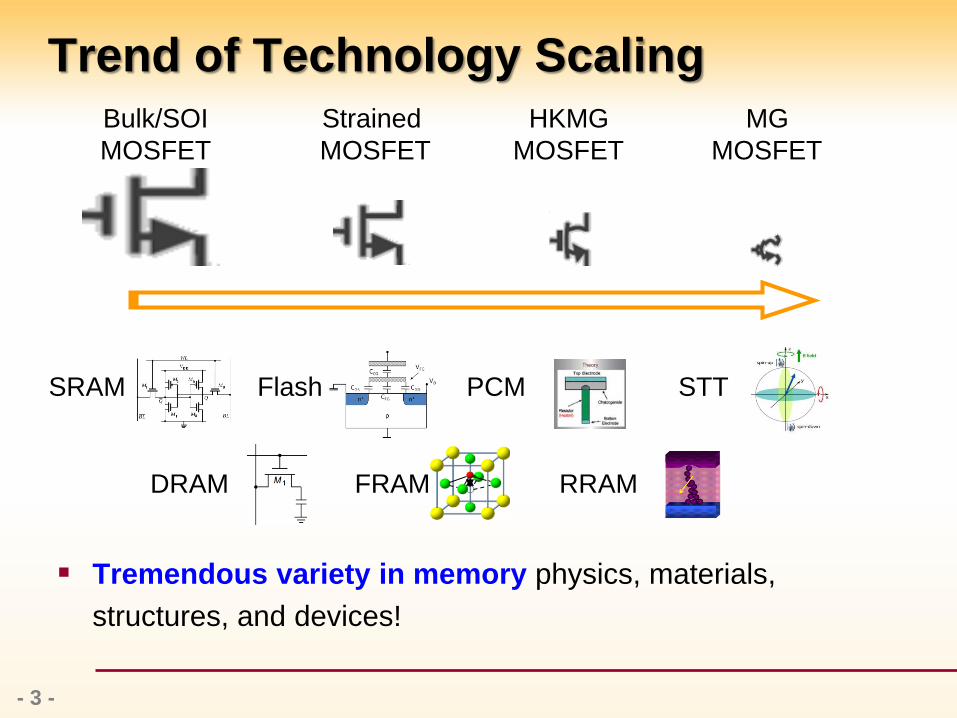
Trend of Technology Scaling
Tremendous variety in memory physics, materials,
structures, and devices!
- 3 -
Bulk/SOI
MOSFET
Strained
MOSFET
HKMG
MOSFET
MG
MOSFET
SRAM
DRAM
Flash
FRAM
PCM
RRAM
STT

Tremendous Diversity
STT-RAM
Advantages:
– Access time comparable to
SRAM
– Density comparable to
DRAM
– Low standby power
– High endurance (>1016)
– Scalable to lower
technology nodes
– Can be used for logic
design
- 4 -
Performance
Read
+ W
rite
Tim
e
Cell Size (F2)
[R. Venkatesan, ISLPED 2012]
STT-RAM
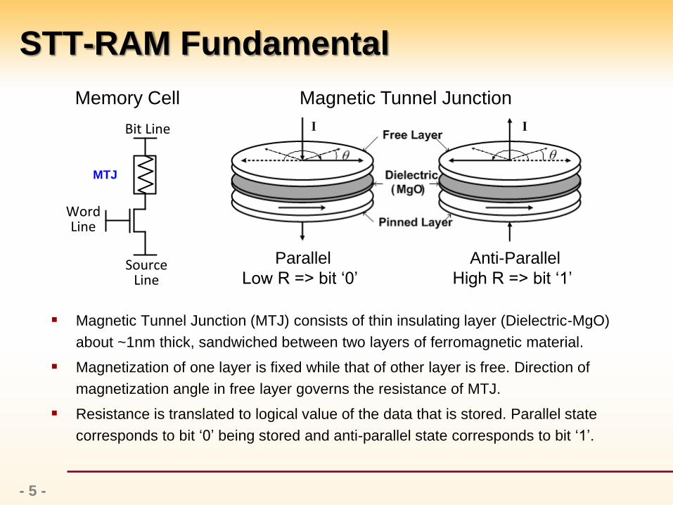
STT-RAM Fundamental
Magnetic Tunnel Junction (MTJ) consists of thin insulating layer (Dielectric-MgO)
about ~1nm thick, sandwiched between two layers of ferromagnetic material.
Magnetization of one layer is fixed while that of other layer is free. Direction of
magnetization angle in free layer governs the resistance of MTJ.
Resistance is translated to logical value of the data that is stored. Parallel state
corresponds to bit ‘0’ being stored and anti-parallel state corresponds to bit ‘1’.
Parallel
Low R => bit ‘0’
Anti-Parallel
High R => bit ‘1’
- 5 -
Bit Line
Word Line
Source Line
Memory Cell
MTJ
Magnetic Tunnel Junction
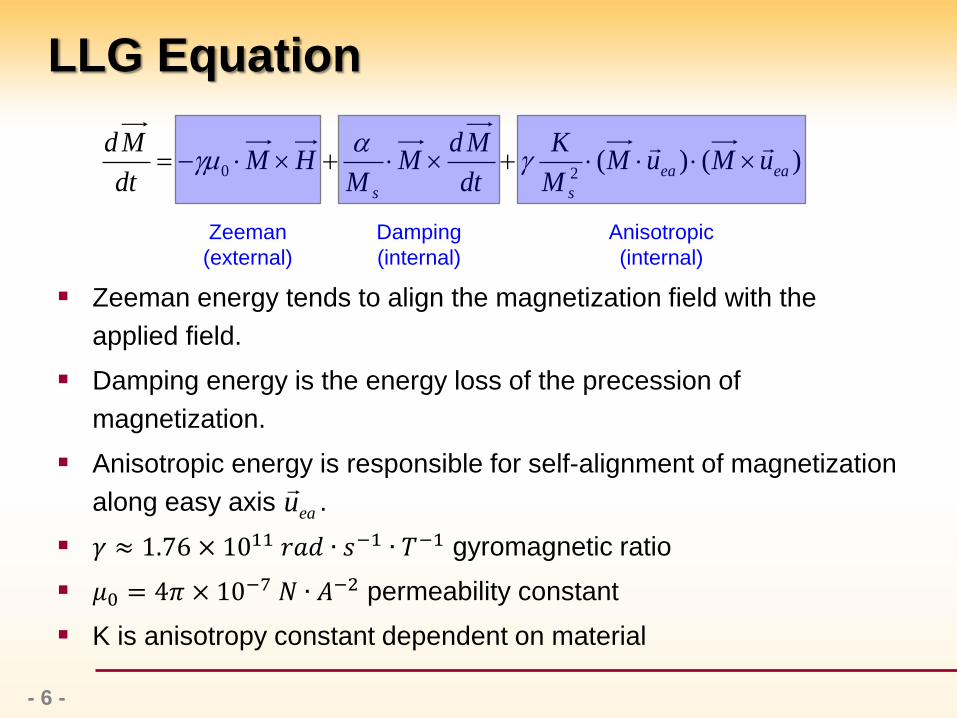
LLG Equation
Zeeman energy tends to align the magnetization field with the
applied field.
Damping energy is the energy loss of the precession of
magnetization.
Anisotropic energy is responsible for self-alignment of magnetization
along easy axis .
𝛾 ≈ 1.76 × 10¹¹ 𝑟𝑎𝑑 ∙ 𝑠−1 ∙ 𝑇−1 gyromagnetic ratio
𝜇0 = 4𝜋 × 10−7 𝑁 ∙ 𝐴−2 permeability constant
K is anisotropy constant dependent on material
)()(20 eaea
ss
uMuMM
K
dt
MdM
MHM
dt
Md
Zeeman
(external)
Damping
(internal)
Anisotropic
(internal)
eau
- 6 -

Numerical Method
Numerically solve 3D LLG equation
Capture both static and transient behavior of
magnetization
Difficult implementation and low efficiency
[J. B. Kammerer, TED 2010]
- 7 -
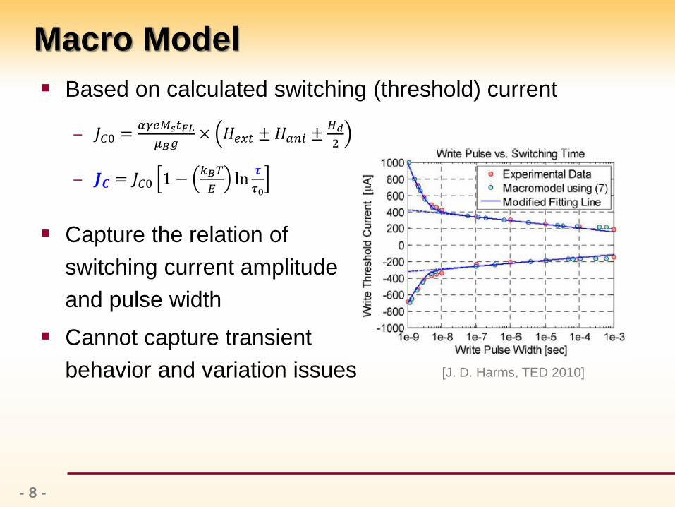
Macro Model
Based on calculated switching (threshold) current
– 𝐽𝐶0 =𝛼𝛾𝑒𝑀𝑠𝑡𝐹𝐿
𝜇𝐵𝑔× 𝐻𝑒𝑥𝑡 ± 𝐻𝑎𝑛𝑖 ±
𝐻𝑑
2
– 𝑱𝑪 = 𝐽𝐶0 1 −𝑘𝐵𝑇
𝐸ln
𝝉
𝜏0
Capture the relation of
switching current amplitude
and pulse width
Cannot capture transient
behavior and variation issues [J. D. Harms, TED 2010]
- 8 -
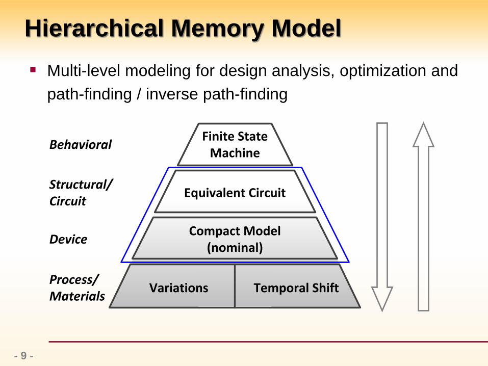
Hierarchical Memory Model
- 9 -
Finite State Machine
Equivalent Circuit
Compact Model (nominal)
Variations Temporal Shift
Behavioral
Structural/Circuit
Device
Process/Materials
Multi-level modeling for design analysis, optimization and
path-finding / inverse path-finding
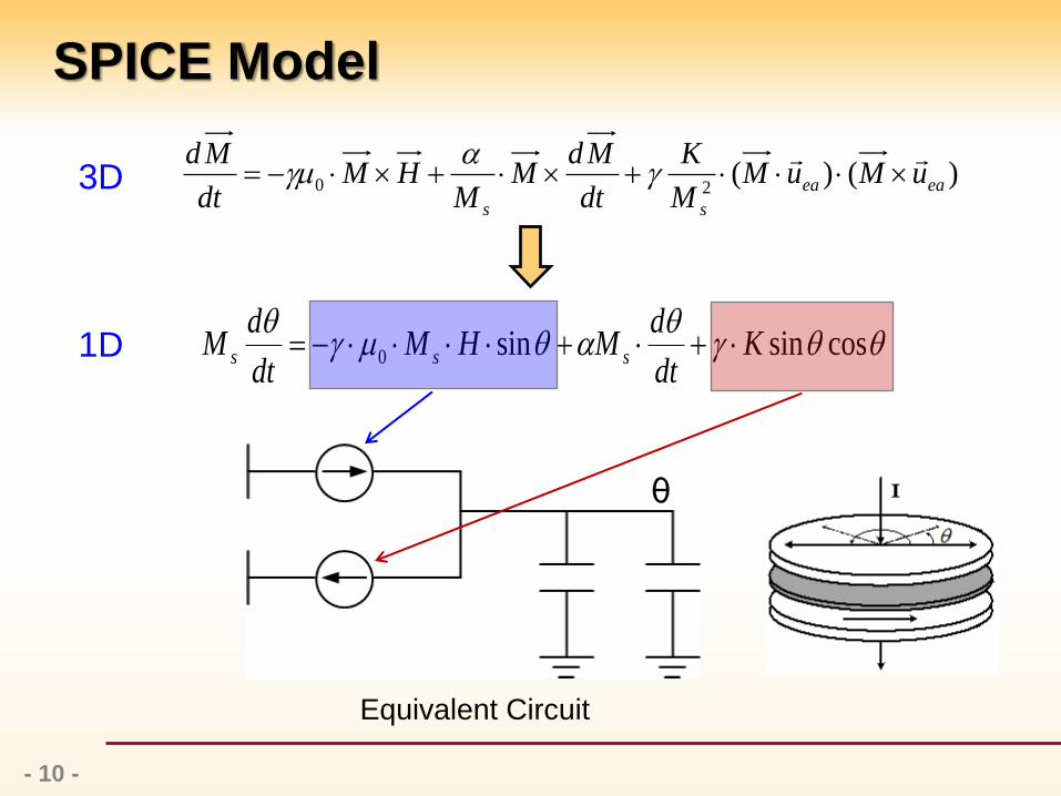
SPICE Model
cossinsin0 Kdt
dMHM
dt
dM sss
- 10 -
)()(20 eaea
ss
uMuMM
K
dt
MdM
MHM
dt
Md
3D
1D
θ
Equivalent Circuit
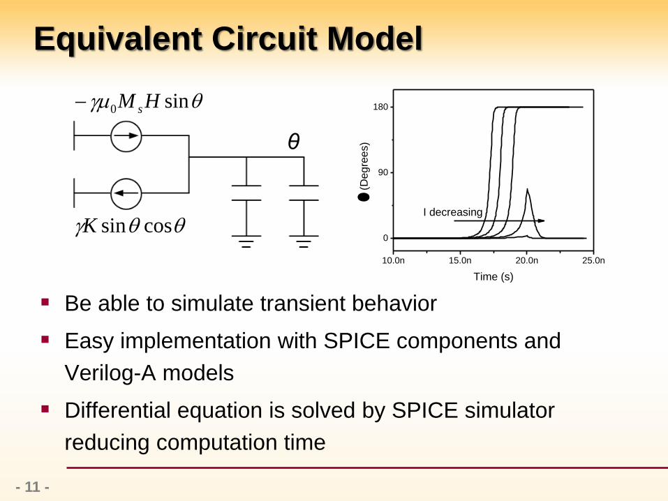
Equivalent Circuit Model
Be able to simulate transient behavior
Easy implementation with SPICE components and
Verilog-A models
Differential equation is solved by SPICE simulator
reducing computation time
sin0 HM s
θ
cossinK
10.0n 15.0n 20.0n 25.0n
Time (s)
0
90
180
(
De
gre
es)
I decreasing
- 11 -

Saturation Magnetization (Ms)
- 12 -
Material and geometry dependent
𝑀𝑠 𝐷
𝑀𝑠0= 4 1 −
1
2𝐷𝑐ℎ
− 1∙ 𝑒𝑥𝑝 −
2𝑆𝑏
3𝑅
1
2𝐷𝑐ℎ
− 1− 3
D: diameter of MTJ layer
Ms0: Ms of bulk ferromagnetic material
c: a constant (0<c≤1) depends on the
interface
h: atomic diameter
Sb: bulk solid-vapour transition entropy
R: ideal gas constant [H. M. Lu, J. Phys. D 2007]
𝑴𝒔
𝑑𝜃
𝑑𝑡= −𝛾 ∙ 𝜇0 ∙ 𝑴𝒔 ∙ 𝐻 ∙ sin 𝜃 + 𝛼𝑴𝒔
𝑑𝜃
𝑑𝑡+ 𝛾 ∙ 𝐾 sin 𝜃 cos 𝜃
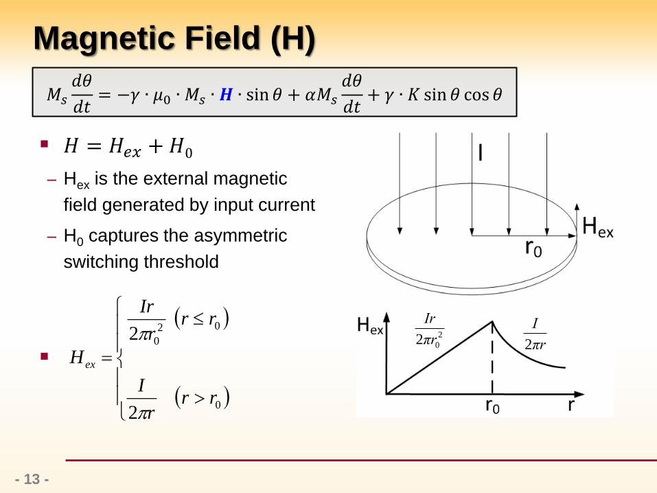
Magnetic Field (H)
𝐻 = 𝐻𝑒𝑥 + 𝐻0
– Hex is the external magnetic
field generated by input current
– H0 captures the asymmetric
switching threshold
𝑀𝑠
𝑑𝜃
𝑑𝑡= −𝛾 ∙ 𝜇0 ∙ 𝑀𝑠 ∙ 𝑯 ∙ sin 𝜃 + 𝛼𝑀𝑠
𝑑𝜃
𝑑𝑡+ 𝛾 ∙ 𝐾 sin 𝜃 cos 𝜃
2
02πr
Ιr
πr
Ι
2
0
02
0
2
2
rrr
I
rrr
Ir
H ex
- 13 -

Magnetic Angle to Resistance
𝑅 = 𝑅𝑃[1 + 0.5𝑇𝑀𝑅(1 − cos 𝜃)]
𝑅𝑃 =𝑡𝑜𝑥
𝐹 𝜑𝐴exp 1.025𝑡𝑜𝑥 𝜑
[J. C. Slonczewski, Phys. Rev. B 2005, Y. Zhang, TED 2012]
As θ approaches 180o, R = RAP
RP RAP
10.0n 15.0n 20.0n 25.0n
(
Deg
ree
s)
R (
)
Time (s)
R1500
2000
2500
0
90
180
tox Oxide thickness 0.85 nm
F Material parameter 332.2
φ Potential barrier 0.4 eV
A Area 3318 nm2
- 14 -

Voltage Dependence of TMR
Tunnel Magnetoresistance (TMR) is the resistance
difference ratio of MTJ of the two states. 𝑇𝑀𝑅 =𝑅𝐴𝑃−𝑅𝑃
𝑅𝑃
TMR depends on the voltage across the MTJ.
– TMR0 is the TMR ratio with
0 voltage.
– Vh is the voltage as
𝑇𝑀𝑅 = 0.5 × 𝑇𝑀𝑅0.
22
0
1 hVV
TMRTMR
2000
3000
4000
5000
Re
sis
tance
(
)
Voltage (mV)
SPICE Model
-300 -200 -100 0 100 200 300
Macro Model [Y. Zhang, TED 2012]
- 15 -
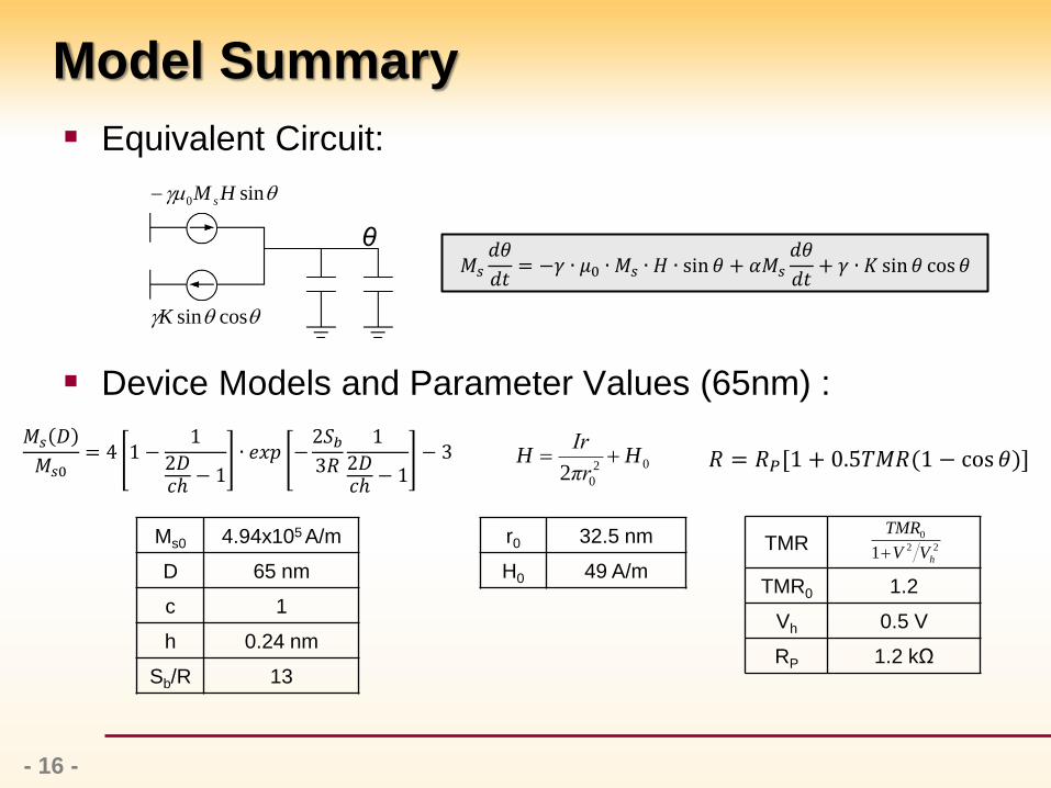
Model Summary
Equivalent Circuit:
Device Models and Parameter Values (65nm) :
sin0 HM s
θ
cossinK
𝑀𝑠
𝑑𝜃
𝑑𝑡= −𝛾 ∙ 𝜇0 ∙ 𝑀𝑠 ∙ 𝐻 ∙ sin 𝜃 + 𝛼𝑀𝑠
𝑑𝜃
𝑑𝑡+ 𝛾 ∙ 𝐾 sin 𝜃 cos 𝜃
𝑀𝑠 𝐷
𝑀𝑠0= 4 1 −
1
2𝐷𝑐ℎ
− 1∙ 𝑒𝑥𝑝 −
2𝑆𝑏
3𝑅
1
2𝐷𝑐ℎ
− 1− 3
02
02H
πr
ΙrH 𝑅 = 𝑅𝑃[1 + 0.5𝑇𝑀𝑅(1 − cos 𝜃)]
Ms0 4.94x10⁵ A/m
D 65 nm
c 1
h 0.24 nm
Sb/R 13
r0 32.5 nm
H0 49 A/m
TMR
TMR0 1.2
Vh 0.5 V
RP 1.2 kΩ
22
0
1 hVV
TMR
- 16 -
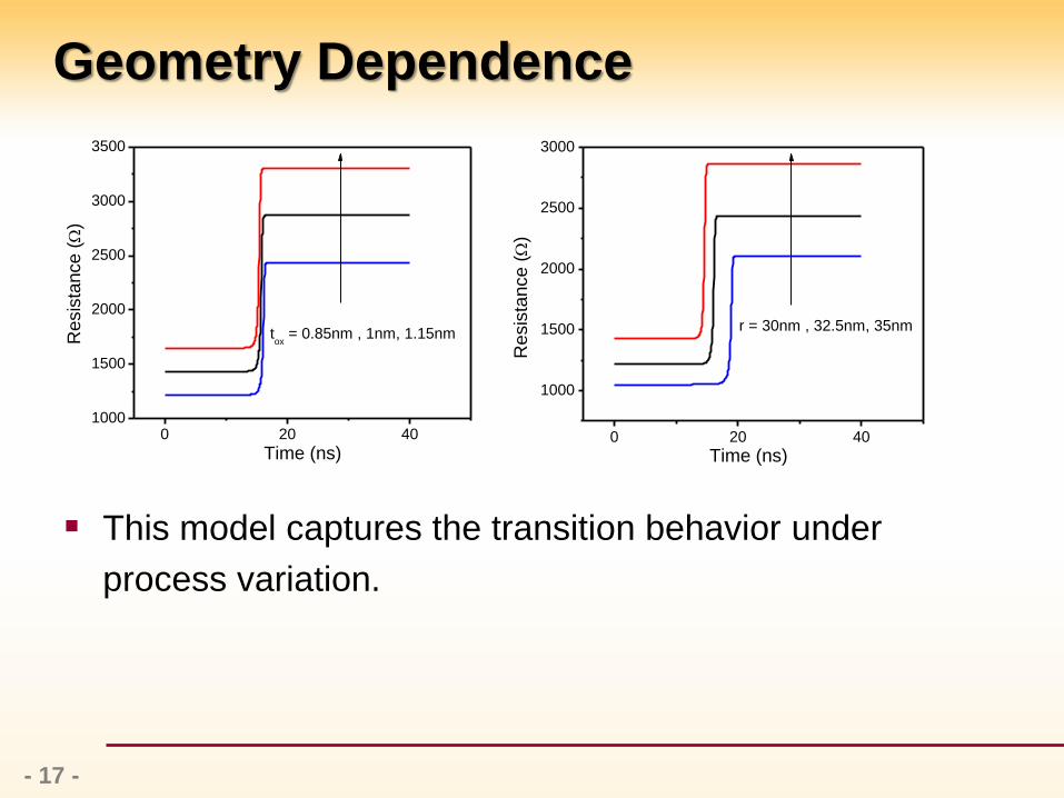
Geometry Dependence
This model captures the transition behavior under
process variation.
- 17 -
0 20 401000
1500
2000
2500
3000
3500
Resis
tance (
)
Time (ns)
tox
= 0.85nm , 1nm, 1.15nm
0 20 40
1000
1500
2000
2500
3000
Resis
tance (
)
Time (ns)
r = 30nm , 32.5nm, 35nm
Temperature Dependence
- 18 -
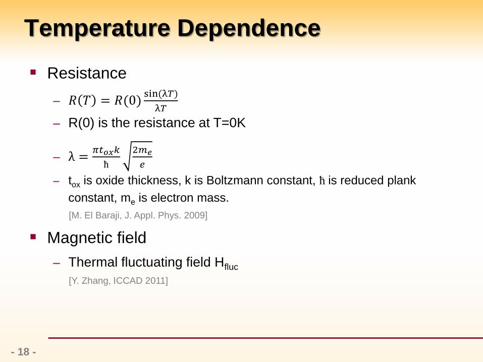
Resistance
– 𝑅 𝑇 = 𝑅(0)sin (λ𝑇)
λ𝑇
– R(0) is the resistance at T=0K
– λ =𝜋𝑡𝑜𝑥𝑘
ћ
2𝑚𝑒
𝑒
– tox is oxide thickness, k is Boltzmann constant, ћ is reduced plank
constant, me is electron mass. [M. El Baraji, J. Appl. Phys. 2009]
Magnetic field
– Thermal fluctuating field Hfluc
[Y. Zhang, ICCAD 2011]
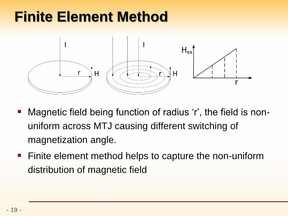
Finite Element Method
Magnetic field being function of radius ‘r’, the field is non-
uniform across MTJ causing different switching of
magnetization angle.
Finite element method helps to capture the non-uniform
distribution of magnetic field
- 19 -
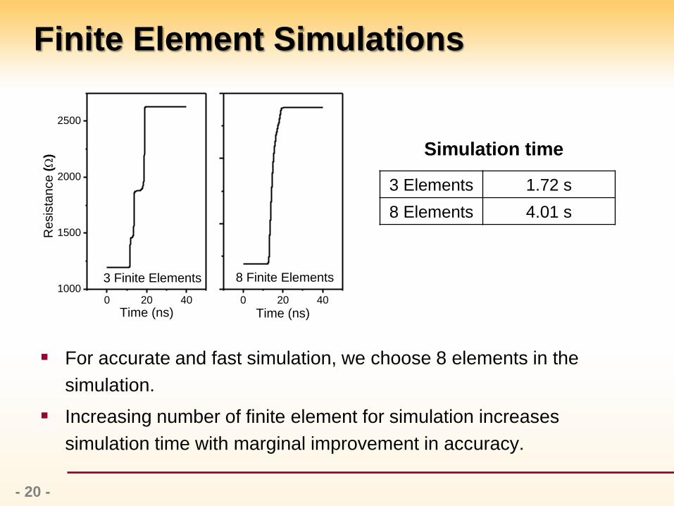
Finite Element Simulations
For accurate and fast simulation, we choose 8 elements in the
simulation.
Increasing number of finite element for simulation increases
simulation time with marginal improvement in accuracy.
0 20 401000
1500
2000
2500
0 20 40
Resis
tance (
)
Time (ns)
3 Finite Elements
Time (ns)
8 Finite Elements
3 Elements 1.72 s
8 Elements 4.01 s
Simulation time
- 20 -

Hysteresis effect predicted by model validated by experimental
data for two different MTJs.
0.4
0.6
0.8
1.0
No
rma
lize
d R
esis
tance
-600.0µ -400.0µ -200.0µ 0.0 200.0µ 400.0µ 600.0µ
Current (A)
[Z. Diao, J. Phys. 2007]
Model Validation
- 21 -

Simulation Setup
Read operation: current lower than critical value is applied to MTJ to
determine its resistance state.
During write operation, BL and SL are charged to opposite values
depending on bit value that is to be stored. For write-0, BL=Vdd,
SL=0V; write-1, BL=0V and SL=Vdd.
Bit Line
Word Line
Source Line
sin0 HM s
θ
cossinK
8X Finite Elements
- 22 -
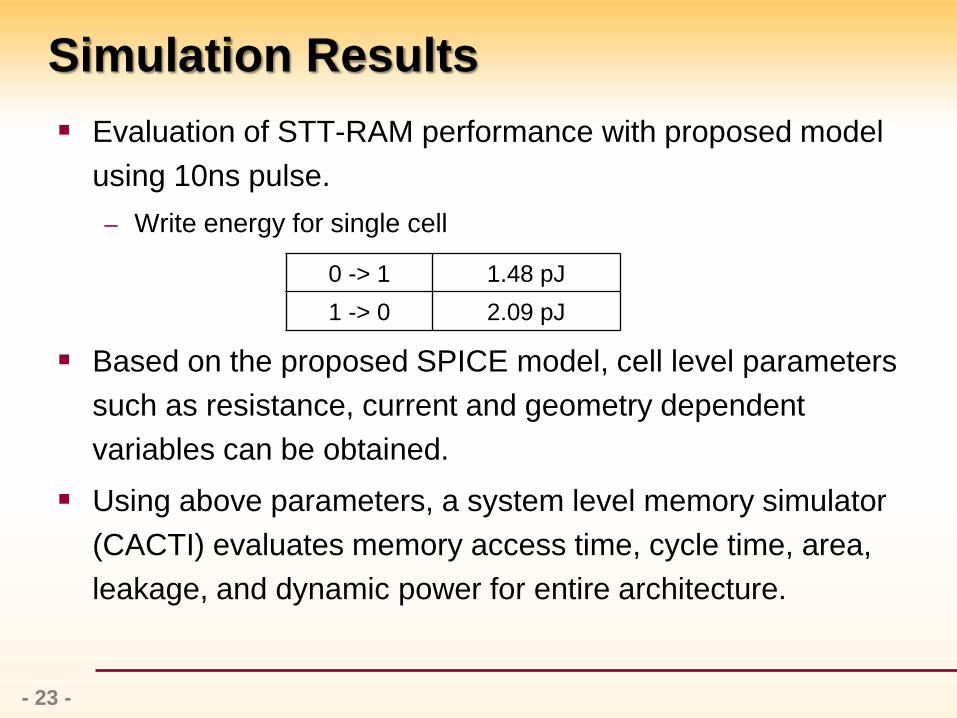
Simulation Results
Evaluation of STT-RAM performance with proposed model
using 10ns pulse.
– Write energy for single cell
Based on the proposed SPICE model, cell level parameters
such as resistance, current and geometry dependent
variables can be obtained.
Using above parameters, a system level memory simulator
(CACTI) evaluates memory access time, cycle time, area,
leakage, and dynamic power for entire architecture.
0 -> 1 1.48 pJ
1 -> 0 2.09 pJ
- 23 -
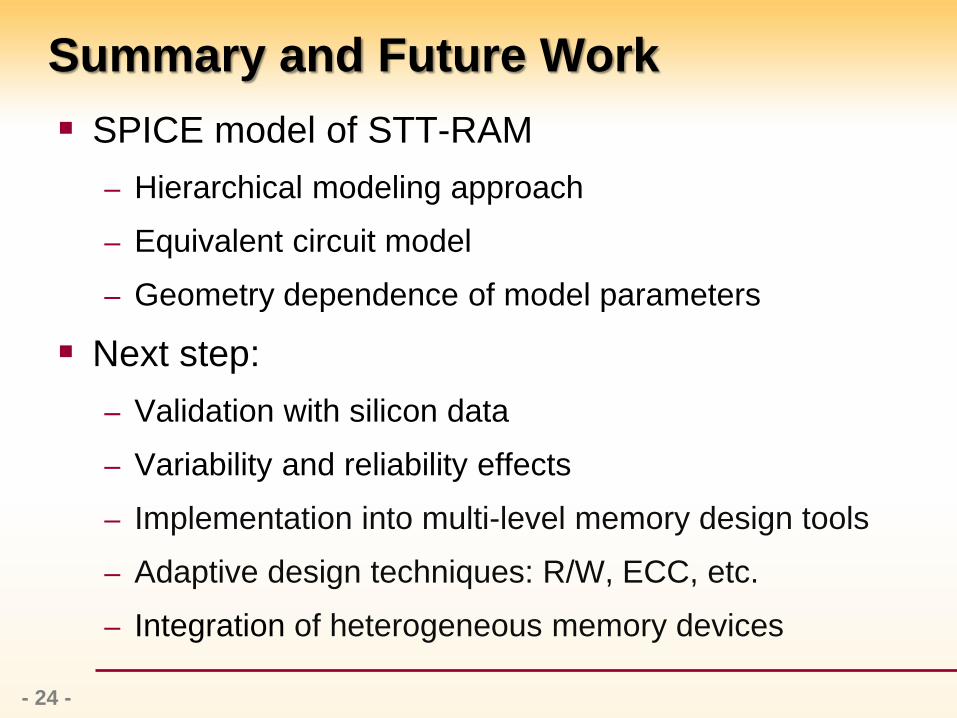
Summary and Future Work
SPICE model of STT-RAM
– Hierarchical modeling approach
– Equivalent circuit model
– Geometry dependence of model parameters
Next step:
– Validation with silicon data
– Variability and reliability effects
– Implementation into multi-level memory design tools
– Adaptive design techniques: R/W, ECC, etc.
– Integration of heterogeneous memory devices
- 24 -