Embed Size (px)
Citation preview

SP
ON
SO
RS

The European Solid-State Devices Research Conference (ESSDERC)and the European Solid-State Circuits Conference (ESSCIRC) arethe premier events in the European research and developmentcalendar. They have a long-established tradition of high-qualitypresentations covering major aspects of solid-state technology,devices, circuits and systems. Since 2002 the ESSCIRC andESSDERC conferences have been organised jointly in recognition ofthe need for the two communities to interact in order to addressthe many challenges faced when designing highly complex systemsin ever more advanced technologies and associated restrictions indesign space.
This year the ESSDERC conference received 165 submissionsoriginating from more than 20 countries, with 101 papers comingfrom Europe, 45 from Asia-Pacific and 16 from the Americas,demonstrating the international nature of ESSDERC. About 20% ofthe submissions came from industry, underlying the relevance ofthe conference. The difficult task of selecting the best papers wascarried out by a 100-strong Technical Programme Committee (TPC)comprising world-class experts from academia, research institutesand industry. The TPC finally selected 71 papers for oralpresentation. All papers received rigorous review with judgementsmade by more than 10 reviewers per paper.
The selected papers are organised in two parallel session trackscomprising three to five presentations. Both traditional and newtopics are evident, namely advanced devices, IC manufacturing,telecommunication, high-voltage and power devices, modelling andsimulation, characterisation and reliability, memory and system-on-chip technologies, sensors, MEMS, flexible electronics,bioelectronics, and emerging devices and nanotechnology. Theseregular sessions are combined with 12 invited papers for bothESSDERC and ESSCIRC. There are six invited speakers who willdeliver joint plenary talks shared between the ESSDERC andESSCIRC conferences, addressing topics of mutual interest,including flexible electronics, 3D integration and energyscavenging, together with perspectives on technology interfacing forfabless design companies, research for the 22 nm node and the
1
WE
LCO
ME
TO
ES
SD
ER
C 2
00
8Welcome toESSDERC 2008

European position around “More Moore and More than Moore”. Inaddition, three speakers have been invited to address theESSDERC community, focusing on topics relating to the futurevision for devices and technology in the areas of memory,germanium, and III-V high-mobility channels and ultimate CMOS.
Three joint sessions have been organised to address topics ofinterest to both device and circuit communities. Two will tackleissues around process stability and yield in the light of the severemanufacturing variability associated with dopant statistics andlinewidth definition, which are becoming evident as devices moveto the atomistic scale. A third joint session will concentrate oncomponents in high-frequency circuits.
The conference programme is complemented by a pre-conference day that is dedicated to tutorials aimed at bothexperienced and early-career research engineers and a post-conference day that includes several workshops.
We would like to thank all of the authors for their excellentcontribution, which has made possible the high quality of theESSDERC 2008 technical and scientific programme. We would alsolike to take this opportunity to acknowledge most warmly all of themembers of the ESSDERC 2008 TPC for their hard work anddedication in their timely reviewing of all of the submitted papersand ensuring a high standard of technical and scientific quality.Particular thanks go to the conference secretariat for handling everyaspect of this complex event with efficiency and competence, andfor their tireless efforts and dedication.
We are looking forward to an exciting and high-level scientificprogramme, combined with many social activities that will give alldelegates the opportunity to network and share experiences whileenjoying the beautiful city of Edinburgh.
Stephen HallESSDERC 2008Technical Programme Committee chair
Anthony WaltonESSDERC 2008General chair
WE
LCO
ME
TO
ES
SD
ER
C 2
00
8
2

AB
OU
T TH
E I
OP
3
The Institute of Physics is a scientific membership organisationdevoted to increasing the understanding and application ofphysics. It has an extensive worldwide membership (currentlyaround 35 000) and is a leading communicator of physics with allaudiences, from specialists through government to the generalpublic. Its publishing company, IOP Publishing, is a world leader inscientific publishing and the electronic dissemination of physics.
For further information about individual membership or how yourcompany can take advantage of the many benefits of the CorporateAffiliates Network, visit us at our stand during the exhibition atESSDERC-ESSCIRC 2008, or go to our website, www.iop.org.Alternatively, contact:
Steve BirdBusiness development managerInstitute of Physics76 Portland PlaceLondonW1B 1NTTel 0207 470 4883E-mail [email protected]
About the IOP

Published byIOP PublishingDirac HouseTemple BackBristolBS1 6BEUKwww.iop.org
ContactTel +44 (0)20 7470 4800 E-mail [email protected] Editorial teamFaye Héran, Lisa Cornwell
Reproduction of any material is subject to editorial authorisation.© The Institute of Physics 2008
ImagesESSCIRC
For further information, visit www.essderc2008.org.
IMP
RIN
T
4

Timetable 6
General information 9
Welcome to Edinburgh 12
Conference site 15
Conference venue 18
Conference facilities 20
Conference registration 22
Conference information 23
Conference overview 24
Meals and refreshments 26
Social programme 27
Accompanying persons programme 29
Exhibition 32
Joint plenary talks 33
ESSDERC plenary talks 37
ESSDERC tutorials 39
ESSDERC programme 52
ESSDERC workshops 64
ESSDERC fringe 72
Notes 75
CO
NTE
NTS
5
Contents
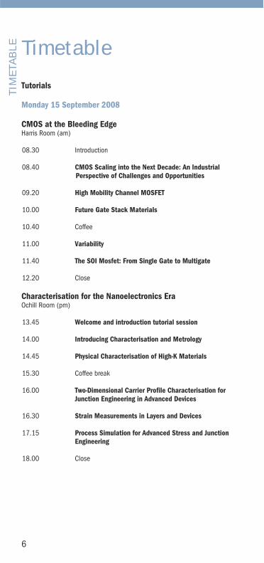
Tutorials
Monday 15 September 2008
CMOS at the Bleeding EdgeHarris Room (am)
08.30 Introduction
08.40 CMOS Scaling into the Next Decade: An IndustrialPerspective of Challenges and Opportunities
09.20 High Mobility Channel MOSFET
10.00 Future Gate Stack Materials
10.40 Coffee
11.00 Variability
11.40 The SOI Mosfet: From Single Gate to Multigate
12.20 Close
Characterisation for the Nanoelectronics EraOchill Room (pm)
13.45 Welcome and introduction tutorial session
14.00 Introducing Characterisation and Metrology
14.45 Physical Characterisation of High-K Materials
15.30 Coffee break
16.00 Two-Dimensional Carrier Profile Characterisation forJunction Engineering in Advanced Devices
16.30 Strain Measurements in Layers and Devices
17.15 Process Simulation for Advanced Stress and JunctionEngineering
18.00 Close
TIM
ETA
BLE
6
Timetable

Integrating CMOS with other TechnologiesMoorfoot Room (pm)
13.30 Introduction to Integrating CMOS with other Technologies
14.10 Design for Manufacture Challenges in MEMS EnabledMicro & Nano Systems
14.50 Post-Processing Microdisplays on CMOS
15.30 Coffee break
15.50 Post-Processing Image Sensors on CMOS
16.30 CMOS Integration with Biotechnology
17.10 Gas Multiplication Grid Integrated on CMOS
17.50 Close
Tuesday 16 September 2008
08.50 Introduction Pentland
09.00–09.40 Joint plenary talk 1 R. Chau, Pentland
09.50–10.50 Process Variability and Yield Joint session, PentlandReliability FintryHigh Voltage Devices Sidlaw
10.50–11.20 Coffee break
11.20–12.50 Channel Engineered Devices FintryAdvanced Analogue Analogue Devices Sidlaw
12.50–14.10 Lunch
14.10–14.50 Joint plenary 2 V. Manian, Pentland
15.00–15.40 ESSDERC plenary 1 T. Hamamoto, Fintry
15.40–16.10 Coffee break and fringe session Cromdale
16.10–17.50 Floating-Gate and Charge-Trap Memories FintryCharacterisation of Advanced Front-End Materials Sidlaw
18.30 Welcome reception, including whisky tastingCromdale Hall
TIM
ETA
BLE
7
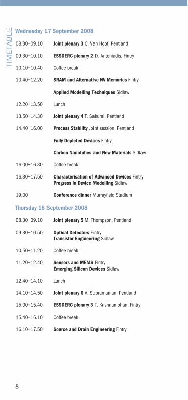
Wednesday 17 September 2008
08.30–09.10 Joint plenary 3 C. Van Hoof, Pentland
09.30–10.10 ESSDERC plenary 2 D. Antoniadis, Fintry
10.10–10.40 Coffee break
10.40–12.20 SRAM and Alternative NV Memories Fintry
Applied Modelling Techniques Sidlaw
12.20–13.50 Lunch
13.50–14.30 Joint plenary 4 T. Sakurai, Pentland
14.40–16.00 Process Stability Joint session, Pentland
Fully Depleted Devices Fintry
Carbon Nanotubes and New Materials Sidlaw
16.00–16.30 Coffee break
16.30–17.50 Characterisation of Advanced Devices FintryProgress in Device Modelling Sidlaw
19.00 Conference dinner Murrayfield Stadium
Thursday 18 September 2008
08.30–09.10 Joint plenary 5 M. Thompson, Pentland
09.30–10.50 Optical Detectors FintryTransistor Engineering Sidlaw
10.50–11.20 Coffee break
11.20–12.40 Sensors and MEMS FintryEmerging Silicon Devices Sidlaw
12.40–14.10 Lunch
14.10–14.50 Joint plenary 6 V. Subramanian, Pentland
15.00–15.40 ESSDERC plenary 3 T. Krishnamohan, Fintry
15.40–16.10 Coffee break
16.10–17.50 Source and Drain Engineering Fintry
TIM
ETA
BLE
8

GE
NE
RA
L IN
FOR
MA
TIO
N
9
General organisationFaye HéranConference organiserTel +44 (0)20 7470 4908Fax +44 (0)20 7470 4900E-mail [email protected]
Programme organisationLisa CornwellProgramme coordinatorTel +44 (0)20 7470 4916Fax +44 (0)20 7470 4900E-mail [email protected]
Conference secretariatThe Institute of Physics 76 Portland PlaceLondon W1B 1NTTel +44 (0)20 7470 4839E-mail [email protected]
Local organisationUniversity of EdinburghScottish Microelectronics CentreKings Building, Edinburgh EH9 3JF, UKTel +44 (0)131 560 5624Fax +44 (0)131 560 6554E-mail [email protected]
Conference chair Anthony Walton, University of Edinburgh Deputy chair Peter Ashburn, University of
Southampton
ESSDERC TPC chair Steve Hall, University of Liverpool Deputy chair Asen Asenov, University of Glasgow Vice-chair A Dimoulas, IMEL/NCSR Demokritos
Tutorial chairsESSDERC Anthony O’Neil, Newcastle University Workshop chair Anthony O’Neil, Newcastle University ESS-fringe poster chairs A J Snell, University of Edinburgh
J T M Stevenson, University of Edinburgh Local chair Les Haworth, University of Edinburgh
Local organising committeeScott Roy University of GlasgowRebecca Cheung University of EdinburghTom Stevenson University of Edinburgh Stewart Smith University of EdinburghJon Terry University of Edinburgh
Steering committeePeter Ashburn University of SouthamptonRoberto Bez ST MicroelectronicsRalf Brederlow Texas InstrumentsCor Clareys (permanent secretary), IMECSorin Cristploveanu ENSERG-IMEP Franz Dielacher InfineonChristian Enz CSEM Gaudenzio Meneghesso University of PadovaHervé Mingam ST MicroelectronicsErneston Perea ST MicroelectronicsHans-Jörg Pfleiderer University of UlmWilliam Redman-White (Vice Chair) NXP/University of
SouthamptonDoris Schmitt-Landsiedel Technical University MunichHannu Tenhunen KTH, StockholmRoland Thewes Qimonda AGReinout Woltjer (chair) NXP
General information

GE
NE
RA
L IN
FOR
MA
TIO
N
10
ESSDERC Technical Programme CommitteeRob Aitken ARMPeter Ashburn University of SouthamptonAsen Asenov University of Glasgow Emmanuel Augendre CEA LETI Jacek Baborowski CSEM (CH)Giorgio Baccarani University of BolognaLivio Baldi St Microelectronics AgrateStefan Bengtsson Chalmers University (S) Anton Bauer FhG, ErlangenRoberto Bez St. Microelectronic Agrate Romuald Beck Wawsaw University of TechnologyStefan Bengtsson Chalmers University (S)Josef Boeck InfineonMizuno Bunji Ultimate Junction Technology LabIngo Bork Synopsys Joachim Burghartz Institute for Microelectronics StuttgartEugenio Cantatore Eindhoven University of TechnologyRaphael Clerc IMEPNadine Collaert IMEC Philippe Coronel STMicroelectronics Crolles (F)Gilles Dambrine IEMNSuman Datta Penn StateStefan Decoutere IMECAn De Keersgieter IMEC Kristin De Meyer IMECBarbara De Salvo CEA-LETI Simon Deleonibus CEA-LETI Bart Dierickx IMECAthanasios Dimoulas NCRS Akis Doganis TSMCKelvin Doong TSMCEmmanuel Dubois IEMNOlof Engström Chalmers University Thomas Ernst CEA-LETI Davide Esseni DIEGM - University of Udine Martin Fallon National Semiconductor UKJuergen Faul QimondaDenis Flandre University Catholique de LouvainHarold Gamble Queens University BelfastFrancisco Gamiz University of GranadaJacques Gautier CEA-LETI (F)Thomas Gessner Chemnitz University of TechnologyGerard Ghibaudo MinatecCarlotta Guiducci University of BolognaStephen Hall University of LiverpoolLuc Haspeslagh IMEC Paul Heremans IMEC (B)Giuseppe Iannacconne University of PisaAdrian Ionescu EPFL LausanneRyoichi Ishihara Tu Delft (NL)Kazunari Ishimaru ToshibaHiroshi Iwai Tokyo Institute of TechnologyHervé Jaouen STMicroelectronics CrollesErich Kasper University of StuttgartFranz Kreupl Qimonda Gilles Le Carval CEA-LETI Tejas Krishnamohan INTEL Salvatoro Lombardo CNR-IMM Jürgen Lorenz, FhG IISB

GE
NE
RA
L IN
FOR
MA
TIO
N
11
Lidia Lukasiak Warsaw University of TechnologyMassimo Macucci University of Pisa (I)Phil Mawby University of Warwick Carlos Mazure SOITECKevin McCarthy University College CorkBernd Meinerzhagen TU BraunschweigRobert Mertens IMECBunji Mizuno Ultimate jn TechVictor Moroz SynopsysMalgorzata Napieralska University of Technology Lodz Androula Nassiopoulou IMEL/NCSR Alexei Nazarov University of Kiev Bich-Yen Nguyen SOITEC Anthony O’Neill University of NewcastleHideki Oka Fujitsu Labs Mikael Östling KTH Davide Pandini St Microelectonics Gianluca Piazza University of Pennsylvania (US)Henryk Przewlocki ITE Warsaw (PL)Massimo Rudan University of BolognaEnrico Sangiorgi University of BolognaAndreas Schenk Integrated Systems Laboratory, ETHZ Jurriaan Schmitz University of Twente (NL) Wim Schoenmaker MAGWELSiegfried Selberherr TU WienLuca Selmi University of Udine (I)Herbert Shea EPF Lausanne/Uni. Neuchatel (CH) Thomas Skotnicki St MicroelectronicsRalph Steiner-Vanha AnalogMichael Stoisiek University of ErlangenYanning Sun IBMEiichi Suzuki National Institute of Advanced Industrial
Science and Technology (AIST)Richard Syms Imperial College (UK)Roland Thewes Qimonda (D)Joseph Tringe Lawrence Livermore Nat. Lab. (US) Dimitris Tsoukalas IMEL/NCRS (GR)Ken Uchida ToshibaMark Van Dal Philips Leuven Gerhard Wachutka Technical University of MunichAndreas Wild Freescale Gilson Wirth University of Porto AllegreReinout Woltjer NXP SemiconductorsJason Woo UCLA Katsunobu Yoshimura Kitakyushu Foundation for the
Advancement of Industriy, Science andTechnology

Edinburgh is located in the south-east of Scotland. It has been thecapital of Scotland since 1437 and is the seat of the ScottishParliament. Owing to its rugged setting and vast collection ofmedieval and Georgian architecture, including numerous stonetenements, it is often considered to be one of the most picturesquecities in Europe. The Old Town and New Town districts of Edinburghwere listed as a UNESCO World Heritage Site in 1995.
The city is well known for the annual Edinburgh Festival – acollection of official and independent festivals held annually overabout four weeks starting in early August. Edinburgh is one ofEurope’s major tourist destinations, attracting around 13 millionvisitors a year, and it is the second most visited tourist destinationin the UK, after London.
ClimateThe climate in Edinburgh is relatively mild in September. However,the weather can change quickly throughout the day – a rainymorning can often be followed by a sunny afternoon. It is thereforeadvisable to come prepared for a mild but rainy climate.
Time zoneWestern Europe daylight/summertime (GMT + 1:00)
ElectricityRequires UK standard three-pin plug, 220–240 V, 50 Hz.
CurrencyThe Scottish currency is the British Pound Sterling. Bank of Englandbanknotes are accepted as legal currency, in addition to those
WE
LCO
ME
TO
ED
INB
UR
GH
12
Welcome to Edinburgh

issued by the Bank of Scotland, the Royal Bank of Scotland andthe Clydesdale Bank. Some retail outlets and visitor attractions willalso accept Euros.
TipsIt is customary to pay 10% in a restaurant or café, although this isonly expected if there is waiter service. If it is a takeaway or self-service establishment you will not be expected to tip.
BanksMost banks are usually open Monday to Friday from 09.30 to16.00/17.00. Some larger branches may also be open later onThursdays and on Saturday mornings. Avoid changing money orcheques in hotels because the rates are usually very poor.
Emergency callsIn case of emergency, dial 999 for the police or fire services.
Passport and visaVisitors from some countries require a visa to enter the UK. Pleasecheck with your travel agent. Participants who require a visa shouldallow plenty of time for their application to be processed. TheInstitute of Physics can issue the standard letter of invitation tothose participants with an accepted presentation at the conferenceand from whom payment has been received in full for theirregistration. For those not making a presentation, the Institute ofPhysics cannot issue invitation letters. Delegates will insteadreceive a letter confirming the conference details and confirmationof payment of registration.
Hotels To arrange accommodation while at the conference, please contactBSI, quoting “IOP” (tel 0870 830 4266; e-mail [email protected]).Information about all hotels can be found in the “Hotels” section of
13
WE
LCO
ME
TO
ED
INB
UR
GH

the websites at www.essderc2008.org and www.esscirc2008.org.
More information about the city is available on the EdinburghTourist Board website at www.edinburgh.org.
WE
LCO
ME
TO
ED
INB
UR
GH
14

The conference, tutorials, workshops and exhibition will be held at:
Edinburgh International Conference Centre (EICC)The ExchangeEdinburgh EH3 8EETel 0131 300 3000 www.eicc.co.uk
How to get to thereThe Edinburgh International Conference is located at the heart ofScotland’s capital city. Its prime central location ensures easyaccess via road, rail and air, and many of its famous and historicalattractions are within walking distance. A range of hotels to suit allbudgets and requirements are also within a short distance of thecentre.
The EICC is arranged over four levels and part of its attraction is theversatility and space available. On arriving in the conference centre,you will find yourself in the Strathblane Hall, where you will be ableto register for the conference.
By planeFor the latest information about flights to Edinburgh, visit thewebsite at www.edinburghairport.com. There are a number of waysto travel into the city centre from the airport, as described below.
By taxiThere is an excellent taxi service direct from the airport to the city.You’ll find official airport taxis at the taxi rank outside the terminalbuilding (follow the signs inside the airport). It costs about £15 toget a taxi from the airport to the city centre and the journey takesaround 20 minutes, depending on traffic flow and time of day.
Local taxi numbersComputer CabsTel 0131 272 8000 www.comcab-edinburgh.co.uk
Festival City CarsTel 0131 552 1777www.festivalcitycars.co.uk
CO
NFE
RE
NC
E S
ITE
15
Conference site

By coachThe Airlink 100 operates a frequent bus service (every 10 minutesat peak times) between Edinburgh Airport and the city centre, withdesignated stops en route. Regular bus services start at 04.45 andrun until 00.22 at night. The journey time is 20 minutes, withtickets costing £3.00 single and £5.00 return. Delegates areadvised to disembark at Haymarket Railway Station and to followsigns for the EICC on foot (a five-minute walk). Also, the N22 busdeparts from stand 19 and runs every 30 minutes through the nightuntil the Airlink service starts again. For more information aboutthese services, visit www.flybybus.com.
By Edinburgh ShuttleThe Edinburgh Shuttle is a door-to-door shared transport servicebetween Edinburgh Airport and the city centre. Fares start at £8.00for an individual with reduced rates for passengers travellingtogether to the same destination. Visit www.edinburghshuttle.comor tel 0845 500 5000.
Arriving by trainEdinburgh has two railway stations: Waverley and Haymarket.Waverley is the main station and has direct routes to many citiesacross the country. For more information, visitwww.nationalrail.co.uk. Haymarket is just a five-minute walk fromthe EICC. Waverley is a few minutes away by taxi.
By busEdinburgh’s main bus terminal is located at St Andrew’s Square.Bus connections stretch right across the UK. For details of theseroutes, visit www.nationalexpress.com or www.citylink.co.uk.
16
HAYMARKETSTATION
BUS
TERMINAL
M8 WESTGLASGOW
M90 NORTHPERTH INVERNESS
A68SOUTHJEDBURGH
NEWCASTLE
M90 NORTHP E R T H
I N V E R N E S S
© Crown copyright. All rights reserved. Licence number WL5214
THEEXCHANGE
CANNING ST
GARD NERSCRESC
ENT
BELGRAVE CRESCENTE T ON T
ERRA
CE
QUEENSFERRYROAD
B E L F O R DR
OAD Q U E E N S F E R R Y
S T R E E T
R A ND O LPHCRES
AIN
S L I E
P LA
CE
LYNEDOCH PLACE
CHESTERSTREET
ROTH
E S A Y T E R R A C E
DRUMSHE UGH GARDENS
MA
NO
RP
LA
CE
M E L V I L L ES T R E E T
STAFFORDSTREET
W I L L I A MS T R E E T
ALVA
STREE
T
COAT
E S CR ES
A T H O L L
CR
ES
MA I T L A N
DS T
S H A ND W
I C KP L A C E
P R I N C E SS T R E E T
M O R R I S O N S T R E E T
LO
TH
IA
NR
OA
D
EARLGREY
DA
LR
YR
OA
D
GR
OV
ES
T RE E T
TORPH ICHEN STREET DEWAR
PL
W E S TA P
PROA
CH
ROAD
SEMPLE
ST
F O U N T A I N B R I D G E
E A S T F O U N T A I N B R I D G EW E S T P O R T
L AUR ISTON PL ACE
T E V I OT
PLA
CE
PO
TTE
RR
OW
CR ICHTON ST
S P I TA L
S T RE E
TC AS
TLE T E R R A C EJ O H N S T ON T E R R A C E
K I N G ’ S S T A B L E S
R O A D
C A ST L E
T E R R A C E
G R I N D L A Y S T
B R E A D S T R E E T
SQUA
RERU T LAN
D RUTLAN
D ST
MO R A Y P L A
CE
ERLANE
WEMYSS PLACE
H E R I O T R O W
HA
NO
VE
RS
TR
EE
T
S TREE TF
RE
DE
RI C
KS
TR
EE
T
ST COLME STREET
Q U E E NS T R E E T
ST
AN
DR
E WS
T RE E T
CH
AR
LO
TT
ES
TR
EE
T
CA
ST L E
ST R
E E T
Y O U N G S T R E E TH I L L S T R E E T
T H I S T L E S T R E E T
NORTHST
DAVIDST
SOUTHDAVID
ST
G E O R G ES T R E E T
ST ANDREW
SQUARE
CHARLOTTE
S Q U A R E
TH
EM
OU
ND
N O R T H B A N K SST
M A R K E T S T R E E T
C A S T L E H I L LL A W N M A R K E T
H I G H S T R E E T
WAV E R
L E YB
RI D
GE
C O C K B U R N S T
NO
RT
HB
RI D
GE
SO
UT
HB
RI D
GE
L E IT H
S TR
E ET
C O W G A T E
C H A M B E R S T R E E T
G R A S S M A R K E T
VI C
T OR I A S T
R O T H E S AYP L A C E
PALMERSTON
PLACE
MO
RR
I S O N L I N K
MELVILLE
CR E S C E N
T
CAMBR
IDGE ST
C A S T L E
E S P L A N A D E
AT HO LL C RESCENT LANE
CANDLEMAKER ROW
BRISTO PL
W E S T P R I N C E S S T R E E T G A R D E N S
EDINBURGHCASTLE
WAVERLEYSTATION
ST JAMESCENTRE
The Exchange, Morrison Street,Edinburgh EH3 8EE.
T: 0131 300 3000 F: 0131 300 3030W: www.eicc.co.uk E: [email protected]
CITY CENTRE MAP The main entrance to the EICC is on Morrison Street where thereis a coach drop off point.
Access to the EICC Loading Bay is from the West Approach Road.
There are a number of car parks within walking distance of theEICC, they are marked on the map. For further details on carparking please visit our website.
Please note that there are a number of one way streets in closeproximity to the EICC.
After 18.30 street parking is allowed in certain areas.
Please be advised that these maps cannot be reproduced withoutthe permission of Ordnance Survey.
A74 SOUTH CARLISLE
Issue No.5
CO
NFE
RE
NC
E S
ITE

By carThe EICC is right in the centre of Edinburgh. The main entrance ison Morrison Street. For directions from your home or office, visitwww.theaa.com and input EH3 8EE for the destination postcodeinto the route planner.
Local busesNumbers 2 and 12 depart approximately 200 yards from theentrance to the EICC on Morrison Street and run every 15 minutesbetween 07.00 and 23.30. There are regular city bus services toLothian Road and Shandwick Place. Delegates should followdirectional signage from Lothian Road and Shandwick Place to theEICC. Buses require the exact change: £1.10 for any journey; daytickets are available for £2.30. For further information, visit theLothian Buses website at www.lothianbuses.co.uk.
CO
NFE
RE
NC
E S
ITE
17
CO
NFE
RE
NC
E V
EN
UE
18
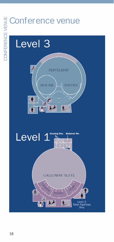
Conference venue

CO
NFE
RE
NC
E V
EN
UE
19

Car parksThere are a number of car parks, all within five minutes’ walkingdistance from the EICC. Local car parks are highlighted on the EICCcity centre map (p16).
Morrison Street car parkCapacity: 400 spaces. Approximate rates: £1.00 (hourly rate)/£5.00 (4–6 h)/£7.20(8 h)/£2.50 (from 17.00 until 07.00).Contact: enquire at the registration desk or tel 0131 477 7000
Semple Street (Thistle Parking)Capacity: 200 spaces. Approximate rates: £1.00 (up to 6 h)/£8.00 (6–10 h)/£10.00(more than 10 h)Contact: tel 0131 225 7480
EICC Morrison Street Capacity: 88 spacesApproximate rates: £1.00 (up to 1 h)/£5.00 (4–6 h)/£7.20 (morethan 8 h)/£2.50 (from 17.00 until 07.00)Contact: enquire at the registration desk or tel 0131 477 7000
Castle Terrace Capacity: 750 spacesOpen 24 hoursApproximate rates: £2.50 (up to 2 h)/£7.00 (4–6 h)/£10.50(9–24 h)/£3.00 (from 17.00 until 06.00)Contact: tel 0131 229 2870
Public phonesFor outgoing calls, coin/card-operated phones are available in theBusiness and Media Centre on Level 0 and near the mainescalator/stairs on Levels 2 and 3.
Cloakroom and toiletsCloakroom facilities can be found next to the lifts in the StrathblaneHall on Level 0. Toilets can be found on every level of theconference centre next to the main escalators/stairs.
Left luggageA left luggage area will be available at the cloakroom in theStrathblane Hall, particularly during peak times for delegate arrival
CO
NFE
RE
NC
E F
AC
ILIT
IES
20
Conference facilities

and departures. Please visit the registration desks near thecloakroom if you have any special requirements.
Drink and food facilitiesThere are coffee/tea machines throughout the venue, all of whichaccept cash. There is also an area in the Strathblane Hall sellingsoft drinks and light snacks.
Disabled accessPlease contact the registration desk or make yourself known to amember of EICC staff, who will assist with any access or facilityrequirements.
Fire and evacuation proceduresFire exits are located in each of the four corners of the building andare well signposted. In the unlikely event of an emergency, pleaseleave the building in an orderly manner, as directed. Do not use themain stairs or escalators. On exiting the building, we will ask you tomove to muster points as advised by the stewards and emergencymarshals.
CO
NFE
RE
NC
E F
AC
ILIT
IES
21

Conference registration deskThe registration desk will be situated in the Strathblane Hall andwill be open throughout the conference at the following times:
Sunday 16.00–19.00Monday 08.00–18.30 Tuesday 08.00–18.30Wednesday 08.00–18.30Thursday 08.00–18.30Friday 08.00–18.00
On arrival, all participants will be given a registration packcontaining conference material and a lapel badge, which must beworn at all times during the conference. Replacement badges canbe issued at the registration desk.
To contact the ESSDERC-ESSCIRC registration desk, tel +44 (0)131519 4123.
MessagesThere will be a message board next to the registration desks in theStrathblane Hall. All messages must be given to a member of theconference team, who will then be able to post them on the board.Plasma screens throughout the EICC will broadcast up-to-dateinformation about the technical programme.
CO
NFE
RE
NC
E R
EG
ISTR
ATI
ON
22
Conference registration

Internet accessWireless internet access will be available throughout the EICC. Thiswill be free of charge during the conference and exhibition, andpasses can be collected from the registration desk throughout theevent. For one-off access to a PC and the internet, there will beseveral computers in the Business and Media Centre, charged atan hourly rate.
Official languageThe congress language is English.
Speakers briefingAuthors should meet their chairperson in the session room20 minutes prior to the beginning of their respective sessions.
Conference proceedingsAll participants will receive a copy of either the ESSDERC or theESSCIRC Proceedings and a USB device containing the acceptedpapers for both.
Best Paper AwardESSDERC/ESSCIRC offers a Best Paper Award (for contributedpapers only) and a Young Scientist Award for the best paperpresented by a speaker under the age of 28. Selection is based onevaluation by the audience and paper ratings.
Insurance disclaimerParticipants are responsible for their own insurance. The Institute ofPhysics, Trinity College and their approved representatives cannottake responsibility for any accident, loss or damage to participantor their property during the event.
ComplaintsWhile we hope that your time at the conference is enjoyable, if youencounter a problem during your stay, please report it to theregistration desk as soon as possible. The conference team willmake every effort to rectify the issue.
CO
NFE
RE
NC
E I
NFO
RM
ATI
ON
23
Conference information

24
CO
NFE
RE
NC
E O
VE
RV
IEW
Sunday 14 September 2008Registration Strathblane Hall
Monday 15 September 2008Registration Strathblane HallTutorials Harris 1, Moorfoot Suite, Kilsyth Suite,
Tinto SuiteBuffet lunch Strathblane HallFringe Cromdale Hall
Tuesday 16 September 2008Registration Strathblane HallConference opening Pentland SuiteTechnical sessions Pentland Suite, Sidlaw Suite, Fintry Suite,
Carrick Suite, Harris 1, Ochil Suite, TintoSuite, Moorfoot Suite, Kilsyth Suite
Buffet lunch Cromdale HallExhibition Cromdale HallFringe Cromdale HallWelcome reception Cromdale HallWomen’s event University of Edinburgh
Wednesday 17 September 2008Registration Strathblane HallTechnical sessions Pentland Suite, Sidlaw Suite, Fintry Suite,
Carrick Suite, Harris 1, Ochil Suite, TintoSuite, Moorfoot Suite, Kilsyth Suite
Buffet lunch Cromdale HallExhibition Cromdale HallFringe Cromdale HallConference dinner Murrayfield Stadium
Thursday 18 September 2008Registration Strathblane HallTechnical sessions Pentland Suite, Sidlaw Suite, Fintry Suite,
Carrick Suite, Harris 1, Ochil Suite, TintoSuite, Moorfoot Suite, Kilsyth Suite
Buffet lunch Cromdale HallExhibition Cromdale HallFringe Cromdale Hall
Conference overview

25
CO
NFE
RE
NC
E O
VE
RV
IEWFriday 19 September 2008
Registration Strathblane HallWorkshops Sidlaw Suite, Carrick Suite, Harris 1, Harris
1, Ochill Suite, Tinto Suite, Moorfoot Suite,Kilsyth Suite
Buffet lunch Stathblane Hall

26
ME
ALS
AN
D R
EFR
ES
HM
EN
TS
All meals and refreshments will be served at allocated times duringthe conference programme.
Monday 15 September 2008Morning refreshments Strathblane HallBuffet lunch Strathblane HallAfternoon refreshments Strathblane Hall
Tuesday 16 September 2008Morning refreshments Cromdale HallBuffet lunch Cromdale HallAfternoon refreshments Cromdale HallWelcome reception Cromdale Hall
Wednesday 17 September 2008Morning refreshments Cromdale HallBuffet lunch Cromdale HallAfternoon refreshments Cromdale HallConference dinner* Murrayfield Stadium
Thursday 18 September 2008Morning refreshments Cromdale HallBuffet lunch Cromdale HallAfternoon refreshments Cromdale Hall
Friday 19 September 2008Morning refreshments Strathblane HallBuffet lunch Strathblane HallAfternoon refreshments Strathblane Hall
*The conference dinner is inclusive in the conference fee and mustbe prebooked. To reserve additional places, [email protected] in advance.
Meals and refreshments

27
Tuesday 16 SeptemberWelcome reception A welcome reception will take place from 18.30 to 20.30 in theCromdale Hall. This will include a whisky-tasting session, offeringdelegates the opportunity to sample traditional whiskies andcheeses from across Scotland. Wine and soft drinks will also beavailable.
Tuesday 16 SeptemberWomen’s event and dinner This will take place in the evening. For further details, pleaseenquire at the registration desk during the conference or refer tothe websites at www.essderc2008.org or www.esscirc2008.org.
Wednesday 17 SeptemberConference dinnerThe conference dinner will be held at Murrayfield Stadium, thehome of Scottish Rugby, from 19.00 to 01.00. It will consist of athree-course Scottish-themed menu in the Thistle and PresidentialSuite and will be preceded by a Pitchside drinks reception (weatherpermitting) with traditional Scottish entertainment. Coaches will beprovided to transport participants to and from the EICC.
Participants with special dietary requirements are asked to notifythe conference organiser prior to their arrival. Unfortunately it willnot be possible to provide an alternative menu unless priornotification has been received.
For further information about Murrayfield Stadium, visit the websiteat www.murrayfieldexperience.com
Social programme
SO
CIA
L P
RO
GR
AM
ME

28
SO
CIA
L P
RO
GR
AM
ME
Travelling to the Murrayfield StadiumShuttle serviceCoaches will be scheduled to take all delegates to and fromMurrayfield Stadium at the following times:.
EICC to Murrayfield StadiumThere will be three pick-ups from the front of the EICC at 18.30,19.00 and 19.30.
Murrayfield Stadium to EICCA shuttle service will run between 22.30 and 24.00, picking upoutside Murrayfield Stadium and dropping off outside the EICC andPrincess Street. For all delegates returning after 24.00, it is advisedthat a private taxi is booked beforehand. Taxi numbers are providedon p15.
Independent travelFor those who wish to arrange independent travel to and fromMurrayfield Stadium, details of the location and directions to thevenue are provided below:
Murrayfield ExperienceEdinburghMidlothian EH12 5PJTel 0131 346 5250 E-mail [email protected]
Murrayfield Stadium is situated in West Edinburgh, six miles fromthe International Airport, three miles from Edinburgh WaverleyRailway Station, one mile from Haymarket Railway Station andclose to the city bypass, and the M8 and M9 motorways. A map of the location is provided below. Please note that the greenarrows are for match-day routes and the red arrows are normalbusiness days.
Gorgie Road
MurryfieldStadium
West Approach Road
Baird Drive
Baird Grove
Saughtonhall DriveBalgreen Road
Westfi
eld R
oad

As a world-class tourist destination, the Edinburgh naturally offers amultitude of activities, whatever time of year you visit. Locatedwithin easy walking distance of the EICC, Edinburgh’s Old Town is afascinating district of cobbled streets, alleys and courtyards. TheRoyal Mile is a clear favourite with visitors, offering a variety ofmuseums, shops and, of course, the world-famous EdinburghCastle. Ghost tours take place every evening around the Old Town,alluding to perhaps the more sinister side of Edinburgh’s past.Open-top bus tours are an excellent way of viewing the whole city.Linking the Old Town with the Royal Yacht Britannia, these exploreEdinburgh’s Georgian New Town and Holyrood Park. Simply hop onand off the bus to visit your favourite attractions.
A list of attractions can be found on the Edinburgh Tourist Boardwebsite at www.edinburgh.org. Some that we particularlyrecommend are listed below.
Dynamic EarthBased in the heart of Edinburgh, Dynamic Earth tells the story ofour planet’s past, present and future. Price per person: adult £9.50/child £5.95 (3–15 years) Opening times: 10.00–18.00 www.dynamicearth.co.uk
29
Accompanying personsprogramme
AC
CO
MP
AN
YIN
G P
ER
SO
NS
PR
OG
RA
MM
E

30
AC
CO
MP
AN
YIN
G P
ER
SO
NS
PR
OG
RA
MM
E
Edinburgh CastleThe castle is the best known and most visited of historic buildingsin the city. Perched on an extinct volcano and offering stunningviews, this instantly recognisable fortress is a powerful nationalsymbol and part of Edinburgh’s world heritage site.Price per person: adult £12.00/Child £6.00 (5–15 years)Opening times: 09.30–18.00www.edinburghcastle.gov.uk
Museum of EdinburghThe Museum of Edinburgh, formerly known as Huntly House,occupies a series of picturesque 16th- and 17th-century buildingsin the heart of the Old Town. It illustrates the history of the city fromthe earliest settlement to the present day. Admission freeOpening times: 10.00–17.00 (Monday to Saturday) www.cac.org.uk
National Museums ScotlandThis family of attractions includes the National Museum ofScotland, the National War Museum, the National Museum ofCostume, the National Museum of Rural Life, the National Museumof Flight and the National Museums Collection Centre. Price per person: varies from free admission to £8.50Opening times: 10.00–17.00 www.nms.ac.uk
The Palace of HolyroodhouseFounded as a monastery in 1128, the palace is The Queen’sofficial residence in Scotland. Situated at the end of the Royal Mile,the it is closely associated with Scotland’s turbulent past, including

31
AC
CO
MP
AN
YIN
G P
ER
SO
NS
PR
OG
RA
MM
EMary, Queen of Scots, who lived here between 1561 and 1567.Successive kings and queens have made the Palace ofHolyroodhouse the premier royal residence in Scotland. Price per person: adult £9.80/child £5.80 (5–17 years)/free(under 5 years)Opening times: 09.30–18.00 (last admission 17:00)www.royal.gov.uk
Edinburgh ZooThe largest and most exciting wildlife attraction in Scotland, the zoois committed to the highest standards of animal welfare,conservation and environmental education. Price per person: adult £11.50/child £8.00 (3–14 years)/free(under 3 years)Opening times: 09.00–18.00www.edinburghzoo.org.uk
Time Out guideTime Out provides an up-to-date guide to accommodation andattractions, a current events calender and restaurant reviews. Theguide for Edinburgh can be found online atwww.timeout.com/travel/edinburgh.
Edinburgh passThe Edinburgh pass offers free travel, plus discounts on shopping,meals and visitor attractions around the city, together with acomprehensive guidebook. Passes range from one to three daysand can be purchased online at www.edinburgh.org/pass, whichalso offers maps, information about the city and suggested itineriesfor a short visit.

32
EX
HIB
ITIO
N
Hosted by JEMI UKwww.jemiuk.com
The exhibition is a new addition to the ESSSDERC/ESSCIRC formatand will include representation from a number of equipment andmaterials suppliers as well as major scientific publishers. It willtake place in the Cromdale Hall on Level 2 and will run fromTuesday 16 To Thursday 18 September. All refreshment and lunchbreaks will be hosted in the exhibition area during the mainconference days, together with the welcome reception on Tuesday16 September and the fringe sessions.
A separate exhibition handbook will be produced and can becollected from the registration desk on arrival.
Opening hoursTuesday 16 September 08:00–18:00Wednesday 17 September 08:00–18:00 Thursday 18 September 08:00–18:00
Exhibition organisersIngrid PrinceBusiness managerJEMI UK Ltd Tel +44 (0)131 650 7815Fax +44 (0)131 650 7475E-mail [email protected]
Exhibition

33
JOIN
T P
LEN
AR
Y T
ALK
S
Emerging Device Nanotechnology for Future High-Speed andEnergy-Efficient VLSI: Challenges and OpportunitiesChau, RobertIntel Corporation
Emerging device nanotechnologies as well as their integration on large siliconwafers present both challenges and opportunities for future high-speed andenergy-efficient digital VLSI applications.aRobert Chau received a BSc, an MS and a PhD in electrical engineering fromOhio State University, Columbus, Ohio. He is an Intel senior fellow and directorof transistor research and nanotechnology at Intel Corporation, Hillsboro,Oregon, and is responsible for directing R&D in advanced transistors and gatedielectrics, process modules and technologies, and integrated processes formicroprocessor applications. He has developed seven generations of Intel gatedielectrics, along with many transistor innovations used in various Intel logicprocesses, since joining Intel in 1989. He is also responsible for leadingresearch efforts in emerging nanotechnologies for future nanoelectronicsapplications. He holds more than 75 US patents and has received six IntelAchievement Awards and 13 Intel Logic Technology Development DivisionRecognition Awards. He was recognised by Industry Week in 2003 as one of the16 “R&D Stars” in the US who “continue to push the boundaries of technicaland scientific achievement”.
Founded in 1968, Intel Corporation is the world’s largest semiconductorcompany and has recently demonstrated a functional 32 nm logic processSRAM with 1.9 B second-generation high-k metal gate transistors.
Technology Interfacing for Fabless Semiconductor CompaniesManian, VahidBroadcom
Today the semiconductor industry faces unprecedented challenges, and thosecompanies that meet these challenges through collaboration, integration andinnovation will be the winners of huge new market opportunities from mobileconvergence to emerging biomedical markets. The semiconductor industry hasmatured and consequently overall revenue growth rates have fallen to singledigits, while the number of units continues to grow robustly. Volume and pricingare on opposite trajectories. The triangulation of increasing volumes; decreasingASPs; and higher R&D investment just to stay in the game is putting seriousprofitability pressure on companies. The design of new products is acceleratingin terms of both costs and complexity. Today it costs a minimum of $15–$30mto reach tape-out, and there doesn’t seem to be an end in sight. Companiescurrently allocate 17% of their revenue to R&D, and this is expected to be 20%by 2012. There are many factors behind this acceleration, including theexponentially growing role of process technology development and softwaredesign. Most leading-edge companies now have more software design engineersthan hardware engineers.
As the cost of developing new process technology increases and building newfabrication facilities grows exponentially, more and more traditional largesemiconductor companies and traditional integrated design manufacturers are
Joint plenary talks
34
JOIN
T P
LEN
AR
Y T
ALK
S migrating to either a fabless model or a fab-light strategy. The fabless businessmodel has clearly won and nearly all companies outside microprocessors andmemory have adopted it. And, despite the reliance on foundries, there are somechallenges that both large and small semiconductor companies face.
Some of the questions facing today’s fabless semiconductor companies are:
� Do we still need specific technology knowledge to support SOCdevelopment?� How much detail do you need in the process technology nodes?� How do we deal with modelling issues?� What is provided from a foundry versus what a company needs?� How do you deal with yield improvement and cost reduction?
Broadcom is one of the early adopters of this business model and has grownfrom zero to a nearly $4bn semiconductor company by adhering to thismodel and navigating through these challenges. We still believe that this is thesuccessful model for the future and need to continue our investment inpartnership with the critical elements of our supply chain
Vahid Manian is the senior vice-president of global manufacturing operationsfor Broadcom Corporation. In this position he is responsible for allmanufacturing activities, including foundry operations and process technologydirection. Manian joined Broadcom in January 1996 as director of operationsand became vice-president of manufacturing operations in December 1997.Previously, he served in a number of positions for approximately 12 years atSilicon Systems Inc, a semiconductor manufacturer, including more than sixyears as director of operations. At Silicon Systems he led the implementation,production ramp and qualification of advanced PRML-read channel integratedcircuits. He received a BSEE and an MBA from the University of California,Irvine.
Micropower Energy Scavengingvan Hoof, ChrisIMEC
More than a decade of research in the field of thermal, motion and vibrationalenergy scavenging has resulted in increasing power output and smallerembodiments. Power-management circuits for rectification and DC–DCconversion are becoming able to convert the power from these energyscavengers efficiently. This paper summarises recent energy-scavenging resultsand their power-management circuits.
Chris Van Hoof received a PhD in electrical engineering from the University ofLeuven, Belgium, in collaboration with IMEC in 1992. He is currently director ofthe Integrated Systems Department of the Microsystems, Components andPackaging Division at IMEC, Leuven, Belgium. At IMEC he became successivelyhead of the detector systems group in 1998, director of the MicrosystemsDepartment in 2002 and director of the Integrated Systems Department in2004. His research concerns several key ingredients of autonomous sensornodes (sensor front-ends, energy scavenging) and is largely focused onadvanced packaging and interconnect technology (2D and 3D integration, RFintegration). Van Hoof has contributed to two cornerstone ESA flight missions.Since 2000 he has also been a guest professor at the University of Leuven, andhe is currently the promoter of eight doctoral theses. He has written more than130 publications and given 20 invited talks.

35
JOIN
T P
LEN
AR
Y T
ALK
SThe Interuniversity Microelectronics Centre (IMEC) is a research facility based inLeuven, with affiliated laboratories throughout Flanders. Its approximately 1500employees focus on next-generation electronics, 3–10 years ahead of industryneeds.
Solving Issues of Integrated Circuits by 3D-Stacking Meetingwith the Era of Power, Integrity Attackers and NRE Explosionand a Bit of FutureSakurai, TakayasuUniversity of Tokyo
In the foreseeable future, VLSI design will meet a few explosions: an explosionof power and an explosion of integrity attackers, including power integrity andsignal integrity, and an explosion of non-recurring engineering cost (NRE). Aremedy for the power explosion and the explosion of integrity attackers lies in“voltage engineering”. A remedy for the NRE explosion is to reduce the numberof developments and sell tens of millions of chips with a fixed design. A 3D-stacked LSI approach may embody such a possibility.
Takayasu Sakuri received his PhD in electrical engineering from the Universityof Tokyo, Japan, in 1981. That year he was with Toshiba Corporation, where hedesigned CMOS DRAM, SRAM, RISC processors, DSPs and SoC Solutions. Hehas worked extensively on interconnect-delay and capacitance modelling,known as the Sakurai model, and an alpha power-law MOS model. From 1988to 1990 he was a visiting researcher with the University of California, Berkeley,where he conducted research in the field of VLSI computer-aided design. Since1996 he has been a professor with the University of Tokyo, working on low-power, high-speed VLSI; memory design; interconnects; and wireless systems.Sakuri has published more than 400 technical papers (including 70 invited)and several books, and he has filed more than 100 patents. He is a consultantto a number of US start-ups. He served as a conference chair for the symposiumon VLSI Circuits and ICICDT, a vice-chair for ASPDAC, a TPC chair for the first A-SSCC and VLSI symposium, and a programme committee member for IEEEISSCC, CICC, DAC, ESSCIRC, ICCAD, ISLPED and other internationalconferences. Sakuri was a plenary speaker for the 2003 ISSC. He is an electedAdCom member for the IEEE Solid-State Circuits Society and a DistinguishedLecturer of the IEEE Circuits and Systems Society. He was a recipient of the2005 IEEE ICICDT Award, the 2005 IEEE ISSCC Takuo Sugano Award and the2005 P&I Patent of the Year Award.
More Than Moore and More Moore in EuropeMichael ThompsonSTMicroelectronics
A brief summary of the trends over the last 10 years for design andmanufacturing activity in Europe is presented, covering the More Moore andMore than Moore technologies. Some of the difficulties in maintaining thetraditional paradigm are then presented, covering the barriers to (re-)entry in theMore Moore field as well as some methods to address them. The samepresentation for the More than Moore field is then made. From this, a number ofconclusions are drawn, including the important role that Europe has to play inshaping design, technology and manufacturing going forward.
Michael Thompson graduated from the University of Glasgow, UK, with a degreein astronomy with advanced mathematics. He started working in 1980 atGeneral Instrument Microelectronics, Glenrothes, as a photolithography
36
JOIN
T P
LEN
AR
Y T
ALK
S engineer, then joined Inmos at Newport, a 100 mm fab specialising in high-performance memories and microprocessors, which was acquired in 1989 tobecome part of SGS-THOMSON, where he worked as process developmentmanager and engineering manager. In 1991 Thompson moved to STMicroelectronics, Crolles, ST’s first 200 mm fab, where he was appointedoperations director. He was involved in the first process technologydevelopment collaboration between ST Microelectronics and Philips from itsstart in 1992, as well as in the creation of the ST Microelectronics–FranceTelecom-CEA/Leti Centre Commun. By 2005 he had the double responsibility ofmanaging the 200 mm fab and contributing to the start-up of Crolles 2, the new300 mm state-of-the-art facility, specialising in high-performance technologiesfor system on chip. He is currently group VP of front-end technology andmanufacturing, advanced R&D — high-performance logic and derivatives.
ST Microelectronics (originally SGS-THOMSON) was formed in 1987 from long-established semiconductor companies SGS Microelettronica and ThomsonSemiconducteurs, It has approximately 50 000 employees, together with 16R&D units and 39 design and application units in front-end technology andmanufacturing.
Printed Electronics for Low-Cost Electronic Systems: TechnologyStatus and Application DevelopmentSubramanian, VivekUniversity of California, Berkeley
Recently, printing has received interest for realising low-cost, large-areaelectronics. It allows additive processing, thus lowering process cost. Coupledwith the use of flexible substrates, printed electronics will enable a range ofelectronic systems, including displays, sensors and RFID tags. We review ourwork on the development of printed electronics. We have realised a range ofprintable electronic “inks”, and used these to demonstrate printed active andpassive components, batteries and various types of gas and biosensor. Byexploiting printing to integrate these cheaply, it is likely that a range ofubiquitous electronic systems will be realised.
Vivek Subramanian received his MSc and PhD in electrical engineering fromStanford University, Stanford, California, in 1996 and 1998, respectively. In1998 he co-founded Matrix Semiconductor Inc. Since 1998 he has been withthe University of California, Berkeley, where he is currently an associateprofessor in the Department of Electrical Engineering and Computer Sciences.He has written more than 50 publications and patents. His research interestsinclude CMOS devices and technology, and polysilicon thin-film transistortechnology for displays and vertical integration applications. His currentresearch focuses on organic electronics for display, low-cost logic and sensingapplications. Subramanian has served on the technical committees for theDevice Research Conference and the International Electron Device Meeting. In2002 he was nominated to Technology Review’s list of top-100 younginnovators and his work at Matrix Semiconductor was nominated to theScientific American SA50 list for visionary technology. In 2003 he wasnominated to the National Academy of Engineering’s Frontiers of Engineeringand was awarded an NSF Young Investigator Award.

Overview and Future Challenges of Floating Body Ram (FBRAM)Technology for 32 nm Technology Node and BeyondHamamoto, TakeshiToshiba Corporation
A floating body cell (FBC) is a one-transistor memory cell on an SOI substrate,which aims high density embedded memory on SOC. In order to verify thismemory-cell technology, a 128 MB floating body RAM with FBC has beendesigned and successfully developed. The memory-cell design and theexperimental results, including the single cell (one cell/bit) operation, arereviewed. Based on the experimental results, the scalability of FBC is alsodiscussed.
Takeshi Hamamoto received his BSc, MSc and PhD from Waseda University,Tokyo, in 1982, 1984 and 1997, respectively. In 1984 he joined the VLSIResearch Centre, Toshiba Corporation, Kawasaki, Japan, where he was engagedin research into memory-cell technologies for high-density DRAMs. From 1989to 1992 he worked on the development of 16 Mb DRAM products, and since1993 he has been engaged in the R&D of device and process technologies forhigh density/high-performance DRAMs. He has been involved in developingNAND structured DRAM cell, 6-F2 layout trench cell, embedded DRAM cell, MIMSTC cell, and Fin Array FET for trench cell. At present, he is a chief specialistwith the Advanced Memory Device Technology Department, Centre forSemiconductor Research and Development, and is developing the technologiesfor SOI and other novel memories. Dr Hamamoto is a member of the JapanSociety of Applied Physics and was a subcommittee member of the IntegratedCircuits and Manufacturing, International Electron Devices Meeting in 2006.
Toshiba Corporation is a high-technology, electrical engineering and electronicsconglomerate based in Tokyo. It was formed in 1939 from two 19th-centurytelegraph and lighting companies, and it currently has 200 000 employees. It isthe third largest semiconductor company in the world by sales.
The Future of High-Performance CMOS: Trends andRequirementsAntoniadis, DimitriMIT
Intrinsic MOSFET time delay is examined as a function of the scaling of high-performance CMOS technology. An analytical expression is used to calculate thedelay from physically meaningful transistor characteristics, which are eitherobtained from the literature or projected forward. The key performanceparameter is the calculated virtual-source carrier velocity in the channel, whichis shown to be responsible for the historical decrease in transistor delay withscaling. The forward projection of transistor delay is based on an optimisticscaling scenario with realistic assumptions about device geometry, electrostaticintegrity and parasitics. It is shown that from the 32 nm CMOS generationonward the intrinsic transistor performance will not improve unless parasiticcapacitances are significantly reduced. Finally, characteristics of performancescaling under localised circuit power density constraints are examined.
Dimitri Antoniadis received his BSc in physics from the National University of
ES
SD
ER
C P
LEN
AR
Y T
ALK
S
37
ESSDERC plenary talks

38
ES
SD
ER
C P
LEN
AR
Y T
ALK
S Athens in 1970 and his PhD in electrical engineering in 1976 from StanfordUniversity. His initial research activities were in the area of the measurementand modelling of the Earth’s ionosphere and thermosphere, ranging frominstrument design to computer simulation. After earning his PhD at Stanford, heled the development of the first two generations of the SUPREM processsimulator, and since then his technical activity has been in the area ofsemiconductor devices and integrated circuit technology. He has worked on thephysics of diffusion in silicon, thin-film technology and devices, and quantum-effect semiconductor devices. His current research focuses on the physics andtechnology of extreme-submicron Si, SOI and Si/SiGe MOSFETs. In 1978,Antoniadis joined the faculty at MIT, where he currently holds the Ray and MariaStata chair in electrical engineering. He was co-founder and first director of theMIT Micro-systems Technology Laboratories and from 1993 to 2000 he wasdirector of the SRC MIT Centre of Excellence for Microsystems Technology.Currently he is director of the multi-university Focus Research Centre forMaterials Structures and Devices centred at MIT. He is the recipient of the SolidState Science and Technology Young Author Award of the ElectrochemicalSociety in 1979, the Paul Rappaport Award of the IEEE in 1998 and the 2002Andrew Grove Award of the IEEE.
High Mobility Ge and III-V Materials and Novel Device Structuresfor High Performance Nanoscale MOSFETSSaraswat, KrishnaStanford University
In order to continue the scaling of silicon-based CMOS and maintain the historicprogress in information processing and transmission, innovative devicestructures and new materials have to be created. A channel material with highmobility and therefore high injection velocity can increase on current and reducedelay. Currently, strained-Si is the dominant technology for high-performanceMOSFETs, and increasing the strain provides a viable solution to scaling.However, looking into the future scaling of nanoscale MOSFETs, it becomesimportant to look at higher-mobility materials, like Ge and III-V materials,together with innovative device structures and strain, which may perform betterthan even very highly strained Si. For both Ge and III-V devices, problems ofleakage need to be solved. Novel heterostructure quantum-well (QW) FETs willbe needed to exploit the promised advantages of Ge and III-V based devices.
Krishna Saraswat received an MSc and a PhD in electrical engineering fromStanford University, California, in 1969 and 1974, respectively. From 1969 hewas with Texas Instruments, engaged in research on microwave transistors.From 1983 he was a professor of electrical engineering at Stanford University,where he developed equipment and simulators for silicon processing. Currentlyhe is the Rickey/Nielsen professor in the School of Engineering, professor ofelectrical engineering, and professor of materials science and engineering (bycourtesy) at Stanford University. Since 2004 he has also been with the BirlaInstitute of Technology and Science as an honorary adjunct professor. He ischair of Stanford’s Materials Council and on the Leadership Council of theMARCO/DARPA-funded Focus Center for Materials, Structures and Nano-Devices. Since the mid-1990s he has been engaged in research on newmaterials, devices, and interconnects for scaling MOS technology to sub-10 nmregime, pioneering several new concepts in 3D ICs. He has guided more than50 doctoral students and written more than 500 technical papers. Saraswat isa recipient of the Thomas Callinan Award from the Electrochemical Society, andthe 2004 IEEE Andrew Grove Award for seminal contributions to silicon processtechnology.

Tutorial 1: CMOS at the Bleeding EdgeHarris RoomOrganiser: Anthony O’Neill, Newcastle University, UK
This tutorial will describe state-of-the-art CMOS from both an industrial and anacademic perspective. Internationally leading experts will give authoritativepresentations on the current status, future directions and challenges facingadvanced silicon technology. The tutorial will appeal to graduate students andyoung engineers who want to gain a broader perspective of the field, as well asto more experienced engineers and managers.
Agenda
08.30 Introduction A O’Neill (Newcastle University, UK)
08.40 CMOS Scaling Into the Next Decade: An Industrial Perspectiveof Challenges and Opportunities P Mahji (Intel/Sematech, USA)
09.20 High Mobility Channel MOSFET S Takagi (Tokyo University,Japan)
10.00 Future Gate Stack Materials O Engstrom (Chalmers University,Sweden)
10.40 Coffee
11.00 Variability A Asenov (Glasgow University)
11.40 The SOI Mosfet: From Single Gate to Multigate J-P Colinge(Tyndall National Institute, Ireland)
12.20 Close
CMOS Scaling Into the Next Decade: An Industrial Perspective of Challengesand OpportunitiesSpeaker: P Mahji, Intel/Sematech
For more than three decades, CMOS scaling has provided the means to realisehigher performance and lower cost/function with every technology node. Thisscaling, often referred to as Moore’s law, has essentially allowed for amonotonic increase in density via geometric scaling while relying onconventional materials. However, as the device dimensions begin to reach thefundamental tolerance limit of conventional materials, the inevitableintroduction of new materials is needed. For example, scaling below 65 nmnode has seen the introduction of high-k dielectrics to curtail the increasing gateleakage. While this introduction has been characterised by Moore himself as thebiggest change in transistor history in the last 40 years, it is becoming clear thatmany more changes involving new materials and/or architecture would benecessary to continue CMOS scaling in the future.
This work will review some of the key highlights of high-k/metal researchworks from various groups and provide an outlook of the primary challenges andopportunities that lie beyond advanced gate stacks, to keep up the scaling
ES
SD
ER
C T
UTO
RIA
LS
39
ESSDERC tutorials

40
ES
SD
ER
C T
UTO
RIA
LS roadmap beyond high-k/metal gates. More specifically, new approaches to formultra-shallow junctions with high active dopant concentrations and low-resistance contacts with novel materials will be presented. Also, critical modulelevel challenges for the potential replacement of Si channel with advanced highmobility channel materials (group IV and III-V) will be discussed. Generally,these high-mobility channel materials have a larger lattice constant, lower band-gap, lower thermal stability and lower dopant solubility limits. Thesecharacteristics directly challenge a) heterogeneous integration on Si platform, b)controlled short channel properties, c) formation of stable gate stacks and d)low external resistance, respectively. Trends, challenges and opportunitiesrelated to several of the aforementioned modules (gate stack, junctions,contacts, and high mobility Ge-based channels) will be briefly presented anddiscussed.
High Mobility Channel MOSFETSpeaker: Shinichi Takagi, The University of Tokyo
Channel engineering is currently recognised as mandatory for future scaledMOSFETs. Among a variety of the channel engineering, I will focus on the currentdrive-enhancement technologies through carrier-transport-enhanced channelsusing strained-Si, Ge and III-V semiconductors in this short course. I will reviewthe basic concept of the choice of channel materials for high-performanceMOSFETs, and address the critical issues for realising CMOS devices using thesechannel materials. I will introduce typical examples of these devices.
Future Gate Stack MaterialsSpeaker: Olof Engstrom, Chalmers University, Sweden
The dielectric material of MOSFET gate stacks has two main purposes: (1) tokeep the electric vector field in the transistor channel under control and (2) tolimit the gate leakage current. The former requirement means that the capacitivecoupling between the gate metal and the channel must be high, which in turninvolves the need for a thin dielectric layer. For an ideally amorphous ormonocrystalline dielectric, the leakage is determined by tunnelling. This,however, requires a thick dielectric or a high value of the “equivalent oxidethickness” (EOT), which can be achieved by a high dielectric constant, k. Also, ahigh energy offset value,���E, between the energy bands of the semiconductorand the dielectric limits leakage by tunneling. As a rule of thumb, in order tofulfil a given field versus leakage requirement, k and �E approximately need tocombine to a minimum product k x �� �� �CE. For the 22 nm LSTP bulk node andbeyond, it is estimated that CE should be about 70 eV and above, while for SOItechnology this value may be lower. In a CMOS process, there are a number ofobstacles to achieve materials with the ideal properties mentioned above,including chemical stability, interface properties and charge carrier traps.Moreover, being influenced also by the properties of the gate metal, thedielectric cannot be treated separately. The whole gate stack, therefore, must beconsidered with a holistic approach. In present gate stack development thebearing is set on rare-earth metal oxides and on ternary compounds based onrare-earth elements. Describing these problems as a background, the talk willdiscuss the prospects of finding gate stack combinations to fulfil therequirements of future CMOS technology.
VariabilitySpeaker: Asen Asenov, University of Glasgow
The variability of the transistor characteristics has become a major concernassociated with CMOS transistors scaling and integration. It already critically

41
ES
SD
ER
C T
UTO
RIA
LSaffects SRAM scaling, and introduces leakage and timing issues in digital logiccircuits. The variability is the main factor restricting the scaling of the supplyvoltage, which for the last three technology generations has remained constant,adding to the looming power crisis.
The tutorial will introduce the different sources of variability on CMOS includingprocess control and uniformity related variability, systematic (deterministic)lithography and stress related variability and statistical variability associatedwith the discreteness of charge and granularity of matter. The main focus of thetutorial will be on the statistical variability, which has become a dominantsource of variability at the 45 nm technology generation and which cannot bereduces by tightening the process control. While in the case of systematicvariability the impact of lithography and stress on the characteristics of anindividual transistor can be modelled or characterised and therefore factored inthe design process, in the case of statistical variability only the statisticalbehaviour of the transistors can be simulated or characterised. Twomacroscopically identical transistors next to each other can have characteristicsfrom the two distant ends of the statistical distribution.
In the tutorial we will review the major sources of statistical variability in nanoCMOS transistors focusing at the 45 nm technology generation and beyond. Thedominant sources of statistical variability including random discrete dopants(Fig.1), like edge roughness (Fig. 2) and poly silicon granularity (Fig. 3) will bediscussed in details.
The SOI MOSFET: From Single Gate to Multigate Speaker: Jean-Pierre ColingeTyndall National Institute, Cork, Ireland
The classical MOSFET is reaching its scaling limits and “end-of-roadmap”alternative devices are being investigated. In a continuous effort to increasecurrent drive and better control short-channel effects, silicon-on-insulator MOStransistors have evolved from classical, planar, single-gate devices into three-dimensional devices with a multi-gate structure (double-, triple- or quadruple-gate devices). It is worth noting that, in most cases, the term “double gate”refers to a single gate electrode that is present on two opposite sides of thedevice. Similarly, the term “triple gate” is used for a single gate electrode that isfolded over three sides of the transistor. This lecture describes the evolution ofMOS transistors from single-gate to multiple-gate structures, the associatedbenefits and potential problems of this technology migration, as well as theemergence of novel quantum effects in small multigate devices.
BiographiesAnthony O’Neill was born in Leicester, England in 1959. He received the BScdegree from the University of Nottingham in 1980 and the PhD degree from theUniversity of St Andrews three years later. Between 1983 and 1986 he workedfor Plessey Research (Caswell) Ltd before taking up his post at the University of
Fig. 1: Random discrete dopants in a 35 nm MOSFET. Fig. 2: Line edgeroughness in a 35 nm MOSFET. Fig. 3 Poly Si granularity in a 35 nm MOSFET.

42
ES
SD
ER
C T
UTO
RIA
LS Newcastle upon Tyne. He has worked on a wide range of topics in the field ofsemiconductor device and process technology and published many papers. In1994 he was Visiting Scientist at MIT (Microsystems Technology Laboratories)and in 2002 he became a Royal Society Industry Fellow with Amtel. He wasappointed to a personal chair in physical electronics and since 1996 has beenSiemans Professor of Microelectronics. He is an IEEE Distinguished Lecturer, aFellow of the IET and a director of the National Microelectronics Institute, UK.Current research interests include Si, strained Si/SiGe and SiC device andprocess technologies and interconnect reliability. He is the chair for tutorialsand workshops at ESSDERC 2008.
Prashant Majhi received his Bachelors of Technology degree from the IndianInstitute of Technology, Madras (1996), and his PhD in science and engineeringof materials program from Arizona State University, Tempe, AZ (2000). Hejoined Phillips Semiconductor in the Netherlands and worked on several CMOSand mixed-signal process technologies. In 2004, he joined Intel Corp., and iscurrently at SEMATECH as an Intel Assignee managing the CMOS scaling group.
Shin-ichi Takagi was born in Tokyo, Japan, on 25 August 1959. He received aBSc, an MSc and a PhD in electronic engineering from the University of Tokyo,Tokyo, Japan, in 1982, 1984 and 1987, respectively. His PhD thesis involvedthe study on the surface carrier transport in MISFETs based on III-Vsemiconductors. He joined the Toshiba Research and Development Center,Kawasaki, Japan, in 1987, where he has been engaged in the research on thedevice physics of Si MOSFETs, including the carrier transport in the inversionlayer, the impact ionisation phenomena, the hot carrier degradation and theelectric properties of Si/SiO2 interface. From 1993 to 1995, he was a VisitingScholar at Stanford University, Stanford, California, where he studied theSi/SiGe hetero-structure devices. Since returning to the ULSI ResearchLaboratories, he was also engaged in the physics and technology of thereliability of SiO2, ferroelectric devices and strained- Si MOS devices. From2001 to 2008, he worked for the MIRAI Project, as the leader of Ultra-HighPerformance New Transistor Structures Theme. In October 2003, he moved tothe University of Tokyo, where he is currently working as a professor in thedepartment of Electronic Engineering, School of Engineering. His recent interestsinclude the science and the technologies of advanced Si CMOS and highperformance CMOS devices using new channel materials, such as strained-Si,Ge and III-Vs. Dr Takagi served on the technical programme committee onseveral international conferences, including the International Electron DeviceMeeting, the International Reliability Physics Symposium, the InternationalConference on Solid State Device and Materials, and the International SolidState Circuits Conference. He is a member of the IEEE Electron Device Societyand the Japan Society of Applied Physics.
Olof Engström received a PhD in solid-state physics from the University of Lundin 1975 and was later employed by ASEA AB for research on high-powerthyristors, by AB Rifa for development of MOS technology and by the SwedishDefence Research Institute for sensor research. In 1984 he came to ChalmersUniversity of Technology as a professor in solid-state electronics. Between 1996and 1999 he served as dean of Chalmers School of Electrical and ComputerEngineering, and from 1999 to 2002 he was director of the MicrotechnologyCenter at Chalmers (MC2). Since 2003 he has been back in research as aprofessor at the Department of Microtechnology and Nanoscience of MC2. Hispresent research interest is in high-k-materials and semiconductor quantumstructures. In 1991 he founded Samba Sensors AB, a company for theproduction of fibre-optical pressure sensors. He is a member of the RoyalSwedish Academy of Engineering Science, the Finnish Society of Science and

43
ES
SD
ER
C T
UTO
RIA
LSthe High-k-Gang (www.high-k-gang.eu).
Asen Asenov received his MSc in solid-state physics from Sofia University,Bulgaria, in 1979 and a PhD in physics from The Bulgarian Academy of Sciencein 1989. He is a professor of Device Modelling, leader of the Glasgow DeviceModelling Group and academic director of the Glasgow Process and DeviceSimulation Centre. He coordinates the development of 2D and 3D quantummechanical, Monte Carlo and classical device simulators and their applicationin the design of advanced and novel CMOS devices. He has pioneered thesimulations of statistical variability in nano-CMOS devices, interface roughnessand line-edge roughness. He has more than 450 publications in the aboveareas.
Jean-Pierre Colinge received a BSc in philosophy, an electrical engineeringdegree and a PhD in applied sciences from the Université Catholique deLouvain, Louvain-la-Neuve, Belgium, in 1980, 1980 and 1984, respectively. Hehas worked at the Centre National d’Etudes des Télécommunications (CNET),Meylan, France, at the Hewlett-Packard Laboratories, Palo Alto, USA, and atIMEC, Leuven, Belgium, where he was involved in SOI technology for VLSI andspecial device applications. From 1991 to 1997, Colinge was professor at theUniversité catholique de Louvain, leading a research team in the field of SOItechnology for low-power, radiation-hard, high-temperature and RF applicationsas well as reduced-dimension devices (thin double-gate and quantum-wireMOSFETs). From 1997 to 2006 he was professor at the University of Californiaat Davis, carrying on research on advanced multigate SOI MOS devices. He hasbeen on the committee of several conferences, including IEDM and SSDM, hasbeen general chairman of the IEEE SOS/SOI Technology Conference in 1988,and is a fellow of IEEE. He has published more than 300 scientific papers andfour books on the field of SOI, as well as two books on semiconductor devicephysics. Colinge is currently professor at the Tyndall National Institute, Ireland,where he is working on the modelling, fabrication and characterisation ofadvanced SOI MOS devices.
Tutorial 2: Characterisation for the Nanoelectronics EraOchill RoomOrganiser: Herman Maes
One of the objectives of the PULLNANO IP-project is to organise trainingsessions and courses for researchers and engineers in Europe, based on theknow-how built up within this project.
The ESSDERC/ESSCIRC 2008 conference has been considered to be a verysuited forum for such a contribution from PULLNANO and more in particular inthe area of characterisation of nanometer technologies and devices on whichsignificant achievements were realised in the course of this project. The topicsthat were selected are related to very challenging issues in the development ofnanometer technologies and devices. These include the characterisation of high-k materials, the characterisation of shallow junctions and the modellingand characterisation of stress and strain. We are pleased to offer a very excitingTutorial program involving an elite group of lecturers who are experts in theirfield and also excellent teachers and who will give a general introduction in theirarea of competence complemented with results from the related researchactivities within PULLNANO.
This tutorial session offers an excellent introduction to the relevant issues and istherefore strongly recommended and is in fact a “must” not only for those whoare starting in this field but also for all physicists and engineers who want to get

44
ES
SD
ER
C T
UTO
RIA
LS familiar with the characterisation issues in these nanometre devices.
We look forward to welcoming you in the Tutorial session in Edinburgh.
Agenda
13.45–14.00 Welcome and introduction to the tutorial session AnthonyO’Neil, Newcastle University, UK & Herman E. Maes, IMEC,Leuven, Belgium
14.00–14.45 Introducing Characterisation and Metrology Tom Stevenson,University of Edinburgh, UK
14.45–15.30 Physical Characterisation of High-K Materials ChristopheWyon, STMicroelectronics, France
15.30–16.00 Coffee break
16.00–16.30 Two-dimensional Carrier Profile Characterisation forJunction Engineering in Advanced Devices Pierre Eyben andWilfried Vandervorst, IMEC, Belgium
16.30–17.15 Strain Measurements in Layers and Devices Alain Claverie,CEMES, France
17.15–18.00 Process Simulation for Advanced Stress and JunctionEngineering Christophe Krzeminski and Evelyne Lampin, IEMN,France
18.00 End of session
Introducing Characterisation and MetrologySpeaker: Tom Stevenson, University of Edinburgh, UK
The tutorial will provide an introductory review of the major metrologytechniques which are used in the microfabrication of devices on silicon, for bothconventional circuits and MEMS devices. When a layer of material is grown ordeposited, process engineers need to monitor and control layer thickness,composition, stress, surface finish, and optical properties. The subsequentphotolithography process has its own set of measurements including resistthickness, critical dimensions (CD) and layer to layer registration (overlay). Theetch process will again require CD measurement as well as layer thickness oretch depth. As dimensions have shrunk on conventional devices, metrologytechniques have had to change in order to resolve and measure the smallerfeatures (CD) and thinner layers. On MEMS devices, the critical dimensions maystill be relatively large and amenable to optical imaging but this approach maybe difficult when layers are tens or hundreds of microns thick. The tutorial willconclude by highlighting some of the major metrology challenges which arepredicted by the roadmap.
Physical Characterisation of High-K Materials Speaker: Christophe Wyon, STMicroelectronics, France
In the frame of the European PullNano project, several techniques for thechemical and morphological characterisation of advanced gate stacks, and inparticular the high κ dielectric, have been investigated. Several practicalaspects of scanning transmission electron microscopy-electron energy loss

45
ES
SD
ER
C T
UTO
RIA
LSspectroscopy (STEM-EELS) and other TEM methods in the application to gatestacks were addressed. High κ/metal gate process was accuratelycharacterised using synchrotron radiation-X-ray photoelectron spectroscopy (SR-XPS). SR-XPS enables the characterisation of buried thin films like interfaciallayers, which usually occur in the high κ process. The on-line monitoring of highκ related processes was successfully achieved using X-Ray Reflectivity (XRR)technique.
Two-dimensional Carrier Profile Characterisation for Junction Engineering inAdvanced Devices Speaker: Pierre Eyben, IMEC, Leuven, Belgium
Junction engineering in advanced devices is a complex task as it requires acomplete understanding of all possible 1D and 2D interactions and theinterplay between preamorphisation steps, halo-implants and LDD/HDD profilesbut equally the impact of (outdiffusion into) liners, details of the gate profileand implant tilt, pile-up during silicidation, stress effects on diffusion andactivation etc. Due to this complexity simple 1D-experiments are no longeradequate and only true 2D-carrier (and dopant) profiles will provide the requiredfundamental understanding. The requirements on the characterisationtechniques for 2D-profiling are very stringent as one needs to combine sub-nmspatial resolution, with a high sensitivity (covering the entire concentration rangeof interest), and accurate quantification. Within the PULLNANO project ScanningSpreading Resistance Microscopy (SSRM) has emerged as the sole methodable to fulfil all these requirements with a resolution as small as 0.5 nm. In thispresentation we will discuss the basic aspects of SSRM, demonstrate itscompliance with all (ITRS)-requirements and demonstrate its application forprocess development and TCAD calibration on planar and FINFET devices.
Strain Measurements in Layers and DevicesSpeaker: Alain Claverie, CEMES, France
While stress in chips has been for long an undesirable effect resulting fromprocessing and/or packaging, strained silicon is now an integral feature of thelatest generation of transistors and electronic devices because of the associatedenhancement in carrier mobility. Different strategies have been used to engineerstrain in devices, leading to complex strain distributions in two and threedimensions. Developing methods of strain measurement at the nanoscale hastherefore been an important objective in recent years but has proved elusive inpractice: none of the existing techniques combines the necessary spatialresolution, precision and field of view. For example, Raman spectroscopy or X-ray diffraction techniques can map strain at the micrometer scale, whereastransmission electron microscopy allows strain measurement at the nanometerscale but only over small sample areas. Along this tutorial, we will review anddiscuss the applicability of these different techniques through technologicallyrelevant examples and present a recently invented technique capable ofbridging this gap and measuring strain to high precision, with nanometre spatialresolution and for micrometer fields of view.
Process Simulation for Advanced Stress and Junction EngineeringSpeaker: Christophe Krzeminski and Evelyne Lampin, IEMN, France
For CMOS devices downscaling, sharp requirements have been defined by theInternational Technology Roadmap for Semiconductors (ITRS) in terms of driveand off state current and power density, making the geometric scaling achallenging task. The new vector largely adopted to extend Moore’s law is themobility enhancement through the introduction of stress by several techniques

46
ES
SD
ER
C T
UTO
RIA
LS (Stress Liner, eSiGe embedded stressor, stress memorisation). On the otherside, a challenging experimental trade-off is being made on jonction processingto meet the sharp requirements in terms of resistance, abruptness and depth.Standard techniques (implantation and rapid thermal annealing) are beingpushed to their limits whereas alternative techniques such as preamorphisation,solid phase epitaxy (SPE), laser annealing and plasma doping are beingoptimised. As will be shown in this session of PULLNANO tutorials, manychallenges are being faced by characterisation methods and metrology tosupport all of this intense research competition. TCAD more generally, andprocess simulation in particular, have a complementary role to play to identifytrade-off and evaluate the scalability. The progresses recently made by standardfinite element based simulators for the modelling of implantation, diffusion andstress engineering will be reviewed and illustrated by examples from differenteuropean projects and from the literature. Furthermore, as the complexityincreases with device downscaling, atomistic simulations are of interest toprovide more understanding and to perform computer experiments in caseswhere the time or atomic scale are very challenging for characterisation. Severalexamples from our recent research work with molecular dynamics in PULLNANOwill be presented.
BiographiesTom Stevenson is operations director of the Scottish Microelectronics Centre,University of Edinburgh, responsible for all aspects of cleanroom operations. Heis also active, in a technical capacity, in a number of research areas, rangingfrom novel device structures to CMP for MEMS devices. His interest in metrologydates back to 1969, when he studied instrument design at the University ofAberdeen (MSc) and thereafter spent five years at Ferranti Ltd, Dalkeith, as adevelopment engineer on moire fringe measuring systems for machine tools andco-ordinate-measuring machines. At the University of Edinburgh his mainresearch interests have been in optical lithography and metrology associatedwith microfabrication of both microelectronic and MEMS devices.
Christophe Wyon has been manager of the ST Crolles Physical Characterisationdepartment since 2002. After receiving a PhD in surface physics and chemistryfrom the National Polytechnique Institute of Grenoble, he joined CEA-LETI forworking on crystal growth of dielectric materials. In 1990 he managed thecrystal growth laboratory before taking the head of Thermal processes and wetchemistry in the Microelectronics Department in 1997. In 1999 ChristopheWyon was in charge of the Physical and Chemical Characterisation laboratory atCEA-LETI. Christophe Wyon led several European projects devoted to thephysical and chemical characterisation and metrology of advanced CMOSprocesses. He is author and co-author of more than 55 international papers.
Pierre Eyben was born in 1975, obtained his MSC in engineering in 1998(Université Liege) and in 2004 his PhD at the K U Leuven with a thesis entitled“Scanning spreading resistance micrsocopy: high-resolution two-dimensionalcarrier profiling of semiconductor structures”. From 2004 to 2006 he worked asa postdoctoral fellow from the IWT (Flemish Institute for Science andTechnology) at IMEC on the further implementation of SSRM and joined Imec in2006, where he is now responsible for the SSRM research and service activities.
Wilfried Vandervorst was born in 1954, obtained his MSc in engineering in1977 and a PhD in 1984 (K U Leuven). He joined IMEC in 1985, where he iscurrently heading the Materials and Components Analysis Group. In 1990 healso became a professor at the K U Leuven and was nominated as Imec fellowin 2001. His prime research is currently focused on the development ofmetrology concepts for the characterisation of advanced devices with a special

47
ES
SD
ER
C T
UTO
RIA
LSemphasis on approaches with high 2D/3D resolution.
Alain Claverie obtained a Dipl Ing in solid-state physics in 1981 from theNational Institute for Applied Science (INSA) of Toulouse, then a PhD in 1984from the University Paul Sabatier of Toulouse. From 1985 he was staff scientist(permanent position) in the semiconductor group at CEMES, an autonomouslaboratory of the National Center for Scientific Research, where he performedexperimental work on the TEM characterisation of ion implanted materials. From1988 to 1993 he was visiting or staff scientist in national laboratories abroad,notably in India (Chandigarh) and California (Berkeley). Claverie’s interestsrange from the nucleation and growth of extended defects and nanoprecipitates,diffusion anomalies in semiconductors and very low energy ion implantation. Heis the author or co-author of more than 150 publications in internationaljournals and serves as a regular reviewer for APL, JAP, PRL, PR and NatureMaterials. He has been the organiser of several international conferences (MRS(3), E-MRS (3), IEEE, GADEST) and is a member of the scientific/technicalboards of several others. Recently he was the coordinator of the EC-supportedNEON (nanoparticles for electronics) a GROWTH Project aimed at engineeringnanocrystals for memory applications. Appointed as directeur de recherches in2002, he is now in the charge of nanoMaterials Group he created at CEMES,where about 30 permanent scientists and about the same number ofpostgraduates and postdocs work on the synthesis, physics, characterisationand integration of nanocrystals and ultrathin films in systems for applications inelectronics, magnetism and optics. E-mail him at [email protected].
Christophe Krzeminski was born in 1975. He received an engineering degreefrom the Institut Supérieur d’Electronique et du Numérique in 1998 and a PhDin electronics from the University of Lille in 2001. From 1998 to 2001 he wasinvolved in the modelling of electronic transport in molecular nanometricelectronics devices. In 2001 he joined the institute d’Electronique, deMicroelectronique et de Nanotechnologie (IEMN) as an assistant professeur inthe Silicon Microelectronics Department. His research was first focused on thedevelopment of a new approach to silicon oxidation and oxynitridationmodelling. In 2003 he joined the Centre de la Recherche Scientifique (CNRS)as a research scientist. His current interests concern the simulation andoptimisation of nanodevices, and the development of continuous and atomisticmodels for silicon process simulation.
Evelyne Lampin (née Martin) is in charge of research at the french NationalCenter of Scientific Research (CNRS). She is working at the Institute ofElectronic, Microelectronic and Nanotechnology (IEMN) close to Lille. Shereceived an engineering degree from ISEN in 1994 and a PhD in materialscience from the University of Lille in 1997. Her dissertation dealt with thecalculation of the electronic states and of the dynamic of carriers in siliconnanostructures. She joined the Silicon Microelectronic Group of the IEMN in1997, where she is studying the physics of advanced silicon technology. Herparticular interest is the modelling of dopant diffusion and activation. Afterdeveloping continuous models of the extended defects formed by ionimplantation, she is now using atomistic methods to study the recrystallisationof silicon after amorphising implants.
Tutorial 3: Integrating CMOS with other TechnologiesPM Moorfoot RoomOrganiser: Jon Terry
The evolution of silicon microelectronics has seen a recent diversification intonew device types and associated novel application areas. Examples of this

48
ES
SD
ER
C T
UTO
RIA
LS diversification include smart power, RF systems, microsystems, microdisplays,bioelectronics and silicon photonics. These technologies have in common theuse of silicon as a platform for system integration with the added value beingthe innovation associated with post-processing of, in many cases, standardfoundry technology. These so-called Silicon+ technologies will most likelybecome the mainstream silicon research direction when scaling has run itscourse and hits a combination of technological and economic barriers.
In this tutorial, experts in academia, start-up technology companies andinternational semiconductor manufacturers will examine the challenges involvedin this exciting field. Existing and potential solutions will be presented and futuredifficulties discussed. A number of case-studies from industry at the forefront ofthis stimulating area will provide invaluable first-hand experience. The tutorialwill appeal to graduate students and young engineers, as well as to moreexperienced engineers and managers who are looking for an informal andinformative introduction to this important field.
Agenda
13.30–14.10 Introduction to Integrating CMOS with other TechnologiesAnthony Walton, University of Edinburgh, UK
14.10–14.50 Design for Manufacture Challenges in MEMS enabled Micro& Nano Systems Andrew Richardson, Lancaster University, UK
14.50–15.30 Post-Processing Microdisplays on CMOS Ian Underwood,Microemissive Displays, UK
15.30–15.50 Coffee break
15.50–16.30 Post-processing Image Sensors on CMOS Lindsay Grant, STMicroelectronics, UK
16.30–17.10 CMOS Integration with Biotechnology Roland Thewes,Qimonda, Germany
17.10–17.50 Gas Multiplication Grid Integrated on CMOS Jurriaan Schmitz,University of Twente, Netherlands
17:50 Close
Introduction to Integrating CMOS with other TechnologiesSpeaker: Anthony Walton, University of Edinburgh, UK
The mainstream IC industry, manufacturing devices such as memories andmicroprocessors, follows the ITRS roadmap towards smaller and smallerdevices. However, in parallel, there is increasing activity involving the integrationof silicon with other technologies and new materials, and it is clear that MEMSwill form an important component of this Silicon+ activity. This tutorial providesan introduction and identifies the options available for integrating MEMS with ICtechnology with examples being used to identify some of the issues associatedwith their implementation.
Design for Manufacture Challenges in MEMS enabled Micro & NanoSystemsSpeaker: Andrew Richardson, Lancaster University
49
ES
SD
ER
C T
UTO
RIA
LSDesign for Manufacture technology has been prioritised, developed and usedwithin the microelectronics community to optimise yield, customise designs tospecific processes and optimise both testability and reliability. MEMSintegration through wafer level packaging and system-in-package technologyopens new challenges within these fields. This presentation will discuss thedesign challenges that relate to manufacturability that need to be addressedbefore routine integration of MEMS into electronic systems can be achieved.Emerging Design-for-X methods including “DfTestability”, “DfReliability” and“DfYield” will be covered with examples of how these techniques can be appliedwithin a systems engineering environment.
Post-processing Microdisplays on CMOSSpeaker: Ian Underwood, Microemissive Displays, UK
This tutorial will broadly review the integration of arrays of light controllingelements on CMOS substrates. It will cover the applications, capabilities andprocess requirements of a number of distinct technologies each of which eitheremits or modulates light. The particular application of microdisplays will be atheme of the tutorial.
Post-processing Image Sensors on CMOSSpeaker: Lindsay Grant, ST Microelectronics, UK
This tutorial will broadly review the integration of arrays of light sensing elementson CMOS substrates. It will cover the technology behind a range of light sensingtechnologies and the processing involved in their integration with othertechnologies. A specific theme of the presentation will be the development andfabrication of CMOS light sensors used in camera chips.
CMOS Integration with BiotechnologySpeaker: Roland Thewes, Qimonda, Germany
There has been significant interest recently with the fabrication of electronicsystems for biotechnology research; terms such as lab-on-a-chip (LOC) havefound their way into everyday use. This tutorial will examine the varioustechnologies involved in the fields of bio molecule detection and nervecell/neural tissue interaction and discuss related advantages and challenges inaccuracy, sensitivity and time-to-result, which have been achieved by theintegration of CMOS control and sensing circuitry with the wet world ofbiotechnology
Gas multiplication grid integrated on CMOSSpeaker: Jurriaan Schmitz, University of Twente, Netherlands
This final tutorial will take the form of a case-study examining the technologywhich has been developed to allow a CMOS (pixel) readout chip to beintegrated with a gas multiplication grid. The resulting system forms anintegrated device that can be applied as a readout device applicable to theincreasingly important field of gaseous detectors.
BiographiesAnthony Walton is professor of microelectronic manufacturing in the School ofEngineering and Electronics at the University of Edinburgh. He leads thetechnology research activities in the Institute for Integrated Micro and NanoSystems (IMNS) and was instrumental in setting up the ScottishMicroelectronics Centre (SMC). This is a purpose-built facility for R&D andcompany incubation consisting of approximately 350 m2 of class-10
50
ES
SD
ER
C T
UTO
RIA
LS cleanrooms. His research interests include the design and fabrication ofmicrosystem technology and its integration with CMOS, which has been afeature of many of the companies that have been spun out of the IMNS. He haspublished more than 200 papers, he is an associate editor of the IEEE’sTransactions on Semiconductor Manufacturing and a member of the IEEE.
Andrew Richardson currently holds a personal chair in microsystemsengineering in the Department of Engineering at Lancaster University. He isdirector of the Centre for Microsystems Engineering and scientific director ofDolphin Integration, Grenoble. He has published 140 journal, conference andworkshop papers, together with two books that cover work in the fields of mixedsignal and analogue design-for-test, defect, fault and degradation modelling,MEMS modelling, and test and design for micro and nanomanufacture. Morerecently he has been carrying out work on system-in-package technology,multisensor microsystems for health monitoring applications, and both bio-MEMS and microfluidics. Richardson has contributed to funded projects in allEuropean IST programmes since 1994. This includes the coordination of theFP6 PATENT-DfMM Network of Excellence that involves 24 partners and morethan 140 researchers across 10 European countries. He is also a partner in theQinetiQ-led integrated project Integrated MNT Platforms & Services(INTEGRAMplus) and is a co-investigator and member of the management teamfor the EPSRC Innovative Electronics Manufacturing Centre. Richardson is also asteering committee member for the NEXUS Association that representsEuropean universities and industry working in the field of integrated MEMS.
Ian Underwood is a co-founder of MED and co-inventor of its P-OLEDmicrodisplay technology. Prior to 1999 he was at the University of Edinburgh,where he carried out pioneering research and development R&D in the field ofliquid-crystal microdisplays between 1983 and 1999. He is a Fulbright fellow(1991), Photonics Spectra Circle of Excellence designer (1994), British Telecomfellow (1997), Ben Sturgeon Award winner (1999), Ernst & Young Entrepreneurof the Year (2003), fellow of the Royal Society of Edinburgh (2004), GannochyMedal winner (2004), fellow of the Royal Academy of Engineering (2008) andfellow of the Institute of Physics (2008). As chief scientific advisor he isresponsible for putting in place projects and programmes to ensure that MED’sfuture products will continue to meet the challenge of fast-moving markets andinnovative customers. He is recognised worldwide as an authority onmicrodisplay technology, systems and applications. In 2005, Underwood wasmade professor of electronic displays at the University of Edinburgh. In additionto his full-time post at MED, he sits on the Council of the ScottishOptoelectronics Association and the Steering Committee of ADRIA (Europe’sNetwork in Advanced Displays). He is co-author of a recently released bookentitled Introduction to Microdisplays.
Lindsay Grant was born in Glasgow, Scotland, in 1961. He received a BSc inphysics from St Andrews University in 1984 and embarked on a career in thesemiconductor industry. He has more than 20 years’ experience insemiconductor device physics and process development. Initially he workednear Bristol, UK, for equipment manufacturer Electrotech on plasma etchprocessing. Then, having moved to Harlow, UK, he spent three years in deviceengineering with STC working on BiCMOS process development. Returning toScotland in 1988 he spent 11 years with Seagate Microelectronics, Livingston.There he worked on bipolar, CMOS, DMOS and BiCMOS technologies and heheld positions in product, device and process engineering. In 1999 he joined STMicroelectronics, Edinburgh. ST acquired VLSI Vision in 1999 and, since then,Grant has played a key role in the development and introduction of CMOSImage Sensor process technology inside ST. He has worked on the development
51
ES
SD
ER
C T
UTO
RIA
LSof seven generations of pixel technology with ST progressing from 5.6 μm pitchin 1999 to 1.4 μm in 2008. He currently holds the position of imaging processdevelopment manager in the Imaging Division. He has written several papers onimaging technology and been an invited speaker at imaging conferences.
Roland Thewes was born in Marl, Germany, in 1962. He received his PhD inelectrical engineering from the University of Dortmund, Germany, in 1995. In1994 he joined the research laboratories of Siemens AG, where he was activein the field of reliability and yield of analogue CMOS circuits, and in the designof non-volatile memories. From 1997 to 1999 he managed projects in the areasof design for manufacturability, reliability, analogue device performance andanalogue CMOS circuit design. From 2000 to 2005 he was responsible for theLab on Mixed-Signal Circuits of Corporate Research of Infineon Technologies,focusing on CMOS-based biosensors, analogue CMOS circuit design and device-circuit interaction. Since 2006 he has been responsible for DRAM core circuitrydevelopment at Qimonda. Moreover, he serves as a consultant of the Max-Planck Society in the area of CMOS-based neural tissue imaging. He has writtenor co-written some 130 technical publications and a similar number of grantedpatents and patent applications. He has served as a member of the technicalprogramme committees of various conferences. Currently he is a member of thetechnical program committees of ISSCC and ESSDERC, of the executivecommittee of IEDM, and of the joint steering committee of ESSDERC/ESSCIRC.
Jurriaan Schmitz (1967) obtained his MSc (1990) and PhD (1994) at theUniversity of Amsterdam in the field of experimental high-energy physics carriedout at NIKHEF. His PhD thesis, supervised by Prof. Jos Engelen, dealt with theR&D of the microstrip gas counter, with the intent to apply it in the ATLAS innerdetector. After his PhD he joined Philips Research (in Eindhoven, Netherlands)to work on CMOS transistor downscaling, and the characterisation and reliabilityof MOS devices. Since 2002 he has been a full professor at the University ofTwente. At present he heads a group of 25 people devoted mainly to scientificresearch on the components inside integrated circuits. His current researchprogramme focuses on CMOS post-processing techniques, details of which canbe found at http://sc.el.utwente.nl/research. He holds 14 US patents and haswritten or co-written more than 80 scientific papers. He is a member of the IEEEand the Dutch and European Physical Societies.

52
ES
SD
ER
C P
RO
GR
AM
ME
Tuesday September 16
08.50 Introduction to ESSDERC and ESSCIRC 2008
A1L-A Joint plenary R. ChauPentlandChair(s): Anthony Walton, University of Edinburgh
Stephen Hall, University of Liverpool
A1L-A1 Emerging Device Nanotechnology for Future High-Speed and 09.00 Energy-Efficient VLSI: Challenges and Opportunities
Robert Chau, Intel Corporation, USA
A2L-A Process Variablilty and Yield Joint sessionPentlandChair(s): Asen Asenov, University of Glasgow
A2L-A1 Experimental Assessment of Logic Circuit Performance 09.50 Variability with Regular Fabrics at 90 nm Technology NodeAuthor(s): Sungdae Choi, University of Tokyo; Katsuyuki Ikeuchi, University
of Tokyo; Hyunkyung Kim, University of Tokyo; Kenichi Inagaki,University of Tokyo; Masami Murakata, SemiconductorTechnology Academic Research Center; Nobuyuki Nishiguchi,Semiconductor Technology Academic Research Center; MakotoTakamiya, University of Tokyo; Takayasu Sakurai, University ofTokyo
A2L-A2 Area/Yield Trade-Offs in Scaled CMOS SRAM Cell10.10Author(s): Vasudha Gupta, Mohab Anis, University of Waterloo
A2L-A3 Evaluation of Intrinsic Parameter Fluctuations on 45, 32 and 10.30 22nm Technology Node LP N-MOSFETsAuthor(s): Binjie Cheng, Scott Roy, Andrew Brown, Campbell Millar, Asen
Asenov, University of Glasgow
A2L-B ReliabilityFintryChair(s): Dimitris Tsoukalas, National Technical University of Athens
Reinout Woltjer, NXP
A2L-B1 A 65 nm Test Structure for the Analysis of NBTI Induced 09.50 Statistical Variation in SRAM TransistorsAuthor(s): Thomas Fischer, Technische Universität München; Ettore
Amirante, Karl Hofmann, Martin Ostermayr, Peter Huber, InfineonTechnologies AG; Doris Schmitt-Landsiedel, TechnischeUniversität München
A2L-B2 An Equivalent Circuit Model for the Recovery Component of 10.10 BTIAuthor(s): Javier Martin-Martinez, Rosana Rodriguez, Montse Nafria, Xavier
Aymerich, Universitat Autònoma de Barcelona; Ben Kaczer, Guido
ESSDERC programme

53
ES
SD
ER
C P
RO
GR
AM
MEGroeseneken, IMEC
A2L-B3 New Floating-Body Effect in Partially Depleted SOI pMOSFET 10.30 Due to Direct-Tunneling Current in the Partial N+ Poly GateAuthor(s): Georges Guegan, Romain Gwoziecki, Patricia Touret, Christine
Raynaud, Simon Deleonibus, CEA LETI – MINATEC; Jeremy Pretet,Olivier Gonnard, Gilles Gouget, STMicroelectronics
A2L-C High Voltage DevicesSidlawChair(s): Mikael Ostling, KTH
Giles Dambrine, IEMN
A2L-C1 High-Voltage Trenched Rectifiers for Smart Power Technology09.50Author(s): Jaume Roig, Bart Desoete, Peter Moens, Filip Bauwens, On
Semiconductor
A2L-C2 DC-Arc Behavior of a Novel Active Fuse10.10Author(s): Joachim Vom Dorp, Friedrich-Alexander University Erlangen-
Nuremberg; Sven Berberich, Anton Bauer, Fraunhofer Institute ofIntegrated Systems and Device Technology; Heiner Ryssel,Friedrich-Alexander University Erlangen-Nuremberg
A2L-C3 Design of Rugged High Voltage High Power P-Channel Silicon 10.30 MOSFET for Plasma ApplicationsAuthor(s) Jinshu Zhang, Dumitru Sdrulla, Dahwen Tsang, Dick Frey, George
Krausse, Microsemi Corporation
10.50 Coffee break
A3L-B Channel Engineered Devices FintryChair(s): Thomas Ernst, CEA LETI
Kristin De Meyer, IMEC
A3L-B1 High Performance 70 nm Gate Length Germanium-On-Insulator 11.20 pMOSFET With High-/Metal GateAuthor(s): Krunoslav Romanjek, CEA LETI – MINATEC; Louis Hutin, CEA LETI;
Cyrille Le Royer, CEA LETI – MINATEC; Arnaud Pouydebasque,Marie-Anne Jaud, CEA LETI; Claude Tabone, CEA LETI – MINATEC;Emmanuel Augendre, Loic Sanchez, Jean-Michel Hartmann, CEALETI; Helen Grampeix, CEA LETI – MINATEC; Vincent Mazzochi,Sébastien Soliveres, Roland Truche, Laurent Clavelier, PascalScheiblin, CEA LETI
A3L-B2 Ge p-channel MOSFETS with La2O3 and Al2O3 GateDielectrics
11.40Author(s): Christophe Rossel, IBM Research GmbH, Zurich Research
Laboratory; Athanasis Dimoulas, NCSR DEMOKRITOS; AxelleTapponnier, Daniele Caimi, David Webb, Caroline Andersson,Marilyne Sousa, Chiara Marchiori, Heinz Siegwart, JeanFompeyrine, Roland Germann, IBM Research GmbH, ZurichResearch Laboratory

54
ES
SD
ER
C P
RO
GR
AM
ME A3L-B3 Atomically Flat Gate Insualtor/Silicon (100) Interface
12.00 Formation Introducing High Mobility, Ultra-low Noise, andSmall Characteristics Variation CMOSF
Author(s): Rihito Kuroda, Akinobu Teramoto, Tomoyuki Suwa, Rui Hasebe,Xiang Li, Masahiro Konda, Shigetoshi Sugawa, Tadahiro Ohmi,Tohoku University
A3L-B4 Poly-Si Stripe TFTs by Grain-Boundary Controlled Crystallization12.20 of Amorphous-Si
Author(s): Ihor Brunets, Jisk Holleman, Alexey Kovalgin, Jurriaan Schmitz,MESA Institute for Nanotechnology, University of Twente
A3L-C Advanced Analogue and RF DevicesSidlawChair(s): Peter Ashburn, University of Southampton
Stefaan Decoutere, IMEC
A3L-C1 Monolithic Integration of CMOS VLSI and CNT for Hybrid 11.20 Nanotechnology ApplicationsAuthor(s): Deji Akinwande, Stanford University; Shinichi Yasuda, Bipul Paul,
Toshiba Corporation Semiconductor Company; Shinobu Fujita,Toshiba Corporation; Gael Close, Philip Wong, Stanford University
A3L-C2 Improved Sub-Threshold Slope in RF Vertical MOSFETS Using a 11.40 Frame Gate ArchitectureAuthor(s): Mohammad Al Hakim, Takashi Uchino, William Redman White,
Peter Ashburn, University of Southampton; Lizhe Tan, OctavianBuiu, Steve Hall, University of Liverpool
A3L-C3 Improved Analog Performance of Strained Si N-MOSFETs on 12.00 Thin SiGe Strained Relaxed BuffersAuthor(s): Olayiwola Alatise, Kelvin Kwa, Sarah Olsen, Anthony O’Neill,
Newcastle University
A3L-C4 Novel Wide-Emitter SiGe HBT Technology for RF Power12.20 ApplicationsAuthor(s): Katsuyoshi Washio, Central Res Lab, Hitachi, Ltd; Hiromi
Shimamoto, Renesas Northern Japan Semiconductor, Inc;Makoto Miura, Katsuya Oda, Central Res Lab, Hitachi, Ltd;
12.50 Lunch
A4L-A Joint plenary V. ManianPentlandChair(s): Bill Redman-White, NXP/University of Southampton
Robert Henderson, University of Edinburgh
A4L-A1 Technology Interfacing for Fabless Semiconductor Companies14.10Author(s): Vahid Manian, Broadcom
A5L-A ESSDERC plenary T. HamamotoFintry Chair(s): Reinout Woltjer, NXP
Roberto Bez, Numonyx
A5L-A1 Overview and Future Challenges of Floating Body Ram

55
ES
SD
ER
C P
RO
GR
AM
ME15.00 (FBRAM) Technology for 32 nm Technology Node and Beyond
Author(s): Takeshi Hamamoto, Takashi Ohsawa, Toshiba Corporation
15.40 Coffee break
A6L-B Floating-Gate and Charge-Trap NAND MemoriesFintryChair(s): Tejas Krishhnamohan, Intel Corporation and Stanford University
Barbara De Salvo, CEA-LETI
A6L-B1 Impact of the Charge Transport in the Conduction Band on the 16.10 Retention of Si-Nitride Based MemoriesAuthor(s): Elisa Vianello, Francesco Driussi, Pierpaolo Palestri, Antonio
Arreghini, David Esseni, Luca Selmi, Università di Udine; NaderAkil, Michiel van Duuren, Dusan Golubovic, NXP-TSMC Res CenterLeuven (BE)
A6L-B2 16-Gigabit, 8-Level NAND Flash Memory with 51 nm 44-Cell16.30 String TechnologyAuthor(s): Tae-Kyung Kim, Sungnam Chang, Seungwan Hong, Dong Hyuk
Chae, Keonho, Jeong-Hyuk Choi, Samsung Electronics Co Ltd
A6L-B3 Si-Nanowire TAHOS (TaN/Al2O3/HfO2/SiO2/Si) Nonvolatile 16.50 Memory cellAuthor(s): Navab Singh, Institute of Microelectronics; J Fu, Institute of
Microelectronics and National University of Singapore; B Yang,Institute of Microelectronics; C Zhu, Institute of Microelectronicsand National University of Singapore; G Lo, D Kwong, Institute ofMicroelectronics
A6L-B4 On the Role of a HTO/Al2O3 Bi-Layer Blocking Oxide in Nitride-17.10 Trap Non-Volatile MemoriesAuthor(s): Marc Bocquet, Gabriel Molas, Luca Perniola, Xavier Garros, Julien
Buckley, Marc Gély, Jean-Philippe Colonna, Helen Grampeix,François Martin, Vincent Vidal, Alain Toffoli, Barbara De Salvo,Simon Deleonibus, CEA LETI – MINATEC; Georges Pananakakis,IMEP/MINATEC/CNRS/INPG; Gérard Ghibaudo, IMEP/LAHC
A6L-B5 Scaling of Floating Gate Electrode for Sub-40 nm Flash 17.30 TechnologiesAuthor(s): Joeri De Vos, Dirk Wellekens, Ingrid Debusschere, Jan Van Houdt,
IMEC; Steven Van Aerde, Pamela Fischer, Peter Zagwijn, ASM
A6L-C Characterisation of Advanced Front-End MaterialsSidlawChair(s): Henryk Przewlocki, Institute of Electron Technology
Stefan Bengtsson, Chalmers University of Technology
A6L-C1 Advantage of La2O3 Gate Dielectric Over HfO2 for Direct 16.10 Contact and Mobility ImprovementAuthor(s): Kuniyuki Kakushima, Kiichi Tachi, Manabu Adachi, Kouichi
Okamoto, Soushi Sato, Jaeyeol Song, Takamasa Kawanago,Parhat Ahmet, Kazuo Tsutsui, Tokyo Institute of Technology;Nobuyuki Sugii, Hitachi, Ltd; Takeo Hattori, Hiroshi Iwai, TokyoInstitute of Technology
A6L-C2 Electron Traps at HfO2/SiOx Interfaces

56
ES
SD
ER
C P
RO
GR
AM
ME 16.30
Author(s): Bahman Raeissi, Yangyin Chen, Johan Piscator, Zonghe Lai, OlofEngström, Chalmers University of Technology
A6L-C3 Origin of the Flat-Band Voltage (Vfb) Roll-Off Phenomenon in 16.50 Metal/High-K Gate StacksAuthor(s): Gennadi Bersuker, C S Park, H C Wen, Kisik Choi, Sematech;
Onise Sharia, Alex Demkov, University of Texas
A6L-C4 Impact of Si-Thickness on Interface and Device Properties for 17.10 Si-Passivated Ge pMOSFETsAuthor(s): Koen Martens, IMEC/Katholieke Universiteit Leuven; Jerome
Mitard, Brice De Jaeger, Marc Meuris, IMEC; Herman Maes, GuidoGroeseneken, IMEC/Katholieke Universiteit Leuven; FrancoMinucci, Felice Crupi, Universita della Calabria
AL6-C5 New Analysis of Heavily Doped Boron and Arsenic in Shallow 17.30 Junctions by X-Ray Photoelectron SpectroscopyAuthor(s): Kazuo Tsutsui, Masamitsu Watanabe, Yasumasa Nakagawa,
Tokyo Institute of Technology; Toru Matsuda, Musashi Institute ofTechnology; Tetsuya Yoshida, Meiji University; Eiji Ikenaga,JASRI/Spring-8; Kuniyuki Kakushima, Parhat Ahmet, TokyoInstitute of Technology; Hiroshi Nohira, Takuya Maruizumi, AtsushiOgura, Meiji University; Musashi Institute of Technology; TakeoHattori, Horoshi Iwai, Tokyo Institute of Technology
Wednesday September 17
B1L-A Joint plenary C. Van HoofPentlandChair(s): Stephen Hall, University of Liverpool
Peter Ashburn, University of Southampton
B1L-A1 Micropower Energy Scavenging08.30Author(s): Paolo Fiorini, Inge Doms, Chris van Hoof, Ruud Vullers, IMEC
B2L-A ESSDERC plenary D. AntoniadisFintryChair(s): Athanasis Dimoulas, NCSR Demokritos
Anthony O’Neill, Newcastle University
B2L-A1 The Future of High-Performance CMOS: Trends and 09.30 RequirementsAuthor(s): Ali Khakifirooz, Dimitri Antoniadis, MIT
B3L-B SRAM and Alternative NV MemoriesFintryChair(s): Roberto Bez, Numonyx
Luc Haspeslagh, IMEC
B3L-B1 Enhancing Noise Margins of FinFET SRAM by Integrating Vth-10.40 Controllable Flexible-Pass-GatesAuthor(s): Kazuhiko Endo, Shin-Ichi O’Uchi, Yuki Ishikawa, Yongxum Liu,
Takashi Matsukawa, Meishoku Masahara, Kunihiro Sakamoto,Junichi Tsukada, Ken-Ichi Ishii, Hiromi Yamauchi, Eiichi Suzuki,National Institute of Advanced Industrial Science and Technology
57
ES
SD
ER
C P
RO
GR
AM
ME
B3L-B2 A Power-Efficient impoved-Stability 6T SRAM Cell in 45 nm 11.00 Multi-Channel FET TechnologyAuthor(s): Olivier Thomas, CEA LETI – MINATEC; Bernard Guillaumot,
STMicroelectronics; Thomas Ernst, CEA LETI; Bastien Cousin,Olivier Rozeau, CEA
B3L-B3 An Integrated Multi-Physics Approach to the Modeling of a 11.20 Phase-Change Memory DeviceAuthor(s): Stefania Braga, Alessandro Cabrini, Guido Torelli, University of
Pavia
B3L-B4 On the RESET-SET Transition in Phase Change Memories11.40 Giuseppina Puzzilli, Fernanda Irrera, Università di Roma La
Sapienza; Paolo Pavan, Luca Larcher, Ankur Arya, Vincenzo DellaMarca, Università di Modena e Reggio Emilia; Andrea Padovani,Università di Ferrara; Agostino Pirovano, STMicroelectronics
B3L-B5 Low Voltage Ferroelectric FET with Sub-100nm Copolymer12.00 P(VDF-TrFE) Gate Dielectric for Non-Volatile 1T MemoryAuthor(s): Giovanni Antonio Salvatore, Didier Bouvet, Igor Stolitchnov, Nava
Setter, Adrian Mihai Ionescu, Ecole Polytechnique Fédérale deLausanne
B3L-C Applied Modelling TechniquesSidlawChair(s): An De Keersgieter, IMEC
B3L-C1 FinFET Stress Engineering Using 3D Mechanical Stress and 2D 10.40 Monte Carlo Device SimulationAuthor(s): Fabian Bufler, Luca Sponton, Axel Erlebach, Synopsys Schweiz
GmbH
B3L-C2 Deterministic Simulation of SiGe HBTs Based on theBoltzmann
11.00 EquationAuthor(s): Sung-Min Hong, Christoph Jungemann, Universität der
Bundeswehr
B3L-C3 Stress Enhancement Concept on Replacement GateTechnology
11.20 with Top-Cut Stress Liner for nFETsAuthor(s): Shinya Yamakawa, Satoru Mayuzumi, Yasushi Tateshita, Hitoshi
Wakabayashi, Ansai Hisaharo, Sony Corporation
B3L-C4 TCAD Analysis for Channel Profile Engineering with Carbon11.40 Doped Si (Si:C) Layer for Post-32 nm Node Bulk Planar
nMOSFETsAuthor(s): Naoki Kusunoki, Akira Hokazono, Shigeru Kawanaka, Ichiro
Mizushima, Hisao Yoshimura, Masaaki Iwai, Fumitomo Matsuoka,Toshiba Corporation Semiconductor Company
B3L-C5 A Compact Model for Undoped Symmetric Double-Gate 12.00 MOSFETs with Schottky-Barrier Source/DrainAuthor(s): Guo Jun Zhu, Xing Zhou, Teck Seng Lee, Lay Kee Ang, Guan Huei
See, Shi Huan Lin, Nanyang Technological University

58
ES
SD
ER
C P
RO
GR
AM
ME B4L-A Joint plenary T.Sakurai
PentlandChair(s): TBC
B4L-A1 Solving Issues of Integrated Circuits by 3D-Stacking Meeting 13.50 with the Era of Power, Integrity Attackers and NRE Explosion
and a Bit of Future
Author(s): Takayasu Sakurai, University of Tokyo B5L-A Process Stability – Joint SessionPentlandChair(s): Asen Asenov, University of Glasgow
B5L-A1 On-Chip Leakage Monitor Circuit to Scan Optimal Reverse Bias 14.40 Voltage for Adaptive Body-Bias Circuit Under Gate Induced
Drain Leakage EffectAuthor(s): Masako Fujii, Hiroaki Suzuki, Hiromi Notani, Hiroshi Makino,
Hirofumi Shinohara, Renesas Tech Corp
B5L-A2 Impact of Strain on LER Variability in bulk MOSFETs15.00Author(s): Xingsheng Wang, Scott Roy, Asen Asenov, University of Glasgow
B5L-A3 On the Stability of Fully Depleted SOI MOSFETs Under15.20 Lithography Process VariationsAuthor(s): Christian Kampen, Tim Fühner, Alexander Burenkov, Andreas
Erdmann, Heiner Ryssel, Fraunhofer Institute of IntegratedSystems and Device Technology
B5L-B Fully Depleted DevicesFintryChair(s): Nadine Collaert, IMEC
Carlos Mazure, SOITEC
B5L-B1 Silicon on Thin BOX (SOTB) CMOS for Ultralow Standby Powerwith Forward-biasing Performance Booster
Author(s): Takashi Ishigaki, Ryuta Tsuchiya, Yusuke Morita, HiroyukiYoshimoto, Nobuyuki Sugii, Hitachi, Ltd; Toshiaki Iwamatsu,Hidekazu Oda, Yasuo Inoue, Renesas Technology Corp; TetsuOhtou, Toshiro Hiramoto, University of Tokyo, Shin’Ichiro Kimura,Hitachi, Ltd
B5L-B2 Metal Gate Thickness Optimization for MuGFET Performance 15.00 ImprovementAuthor(s): Isabelle Ferain, IMEC/Katholieke Universiteit Leuven; Nadine
Collaert, Barry O’Sullivan, Thierry Conard, Mihaela Popovici, SvenVan Elshocht, IMEC; Johan Swerts, ASM Belgium; MalgorzataJurczak, IMEC; Kristin De Meyer, IMEC/Katholieke UniversiteitLeuven
B5L-B3 FDSOI Devices with Thin BOX and Ground Plane Integration for 15.20 32 nm Node and BelowAuthor(s): Claire Fenouillet-Béranger, Stephane Denorme,
STMicroelectronics; Pierre Perreau, CEA LETI; Christel Buj-Dufournet, Olivier Faynot, François Andrieu, Lucie Tosti, CEA LETI– MINATEC; Sebastien Barnola, Thierry Salvetat, CEA LETI; XavierGarros, CEA LETI – MINATEC; Mikael Casse, CEA LETI; Fabienne

59
ES
SD
ER
C P
RO
GR
AM
MEAllain, CEA LETI – MINATEC; Nicolas Loubet, STMicroelectronics;
Loan Pham-Nguyen, STMicroelectronics/IMEP; Emilie Deloffre,STMicroelectronics
B5L-B4 Folded Fully Depleted Bulk+ Technology as a Highly W-Scaled 15.40 Planar SolutionAuthor(s): Gregory Bidal, Nicolas Loubet, Claire Fenouillet-Béranger,
Stephane Denorme, STMicroelectronics; Pierre Perreau, CEA LETI;Daniel Chanemougame, Cyrille Laviron, François Leverd,STMicroelectronics; Sebastien Barnola, CEA LETI; R Beneyton, CDuluard, J Chapon, P Gouraud, T Salvetat, M Grosjean,STMicroelectronics
B5L-C Carbon Nanotubes and New MaterialsSidlawChair(s): Franz Kreupl, Qimonda
Adrian Ionescu, EPFL
B5L-C1 Reduction of the Dark-Current in Carbon Nanotube Photo-14.40 DetectorsAuthor(s): Mahdi Pourfath, Hans Kosina, Vienna University of Technology;
Siegfried Selberherr, Vienna University of Technology/Institute forMicroelectronics
B5L-C2 Integration of Resistive Switching NiO in Small via Structures15.00 from Localized Oxidation of Nickel Metallic LayerAuthor(s): Lorene Courtade, Christian Turquat, Institut Materiaux
Microelectronique et Nanosciences de Provence; Judit Lisoni,Ludovic Goux, Dirk Wouters, Interuniversity MicroElectronicsCenter; Damien Deleruyelle, Christophe Muller, Institut MateriauxMicroelectronique et Nanosciences de Provence
B5L-C3 An Analytical Model for Intrinsic Carbon Nanotube FETs15.20Author(s): Lan Wei, Stanford University; David Frank, Leland Chang, IBM
Research; Philip Wong, Stanford University
B5L-C4 Study of Ferrocene/Silicon Hybrid Memories: Influence of the 15.40 Chemical Linkers and Device Thermal StabilityAuthor(s): Tiziana Pro, CEA LETI; Julien Buckley, CEA LETI – MINATEC; R
Barattin, A Calborean, CEA LETI; Marc Gély, CEA LETI – MINATEC;K Huang, G Delapierre, F Duclairoir, E Jalaguier, P Maldivi, CEALETI;, Barbara De Salvo, Simon Deleonibus, CEA LETI – MINATEC;Gérard Ghibaudo, IMEP/LAHC
16.00 Coffee break
B6L-B Characterisation of Advanced DevicesFintryChair(s): Ken Uchida, Tokyo Institute of Technology
Atanasis Dimoulas, NCSR Demokritos
B6L-B1 A Mobility Extraction Method for 3D Multichannel Devices16.30Author(s): Thomas Ernst, Cécilia Dupré, CEA LETI; Emilie Bernard, Bernard
Guillaumot, Nathalie Vulliet, Philippe Coronel, Thomas Skotnicki,STMicroelectronics; Sorin Cristoloveanu, CNRS/IMEP; Gérard
60
ES
SD
ER
C P
RO
GR
AM
ME Ghibaudo, IMEP/LAHC; Simon Deleonibus, CEA LETI – MINATEC
B6L-B2 Experimental and Theoretical Analysis of Hole Transport in 16.50 Uniaxially Strained pMOSFETsAuthor(s): Karim Huet, University Paris-Sud/CNRS/STMicroelectronics;
Maxime Feraille, Denis Rideau, Romain Delamare,STMicroelectronics; Valerie Aubry-Fortuna, CNRS; MoustafaKasbari, Sylvain Blayac, Ecole des Mines de Saint-Etienne, Centrede Microelectronique de Provence; Christian Rivero,STMicroelectronics Rousset; Arnaud Bournel, University Paris-Sud;Clément Tavernier, STMicroelectronics Crolles; Philippe Dollfus,CNRS; Herve Jaouen, STMicroelectronics Crolles
B6L-B3 Influence of Gate Underlap in AM and IM MuGFETs17.10Author(s): Chi-Woo Lee, Aryan Afzalian, Ran Yan, Nima Dehdashti, Jean-
Pierre Colinge, Tyndall National Institute, University College Cork;Weize Xiong, Texas Instruments Inc
B6L-B4 Extracting Energy Band Offsets on Thin Silicon-on-Insulator 17.30 MOSFETsAuthor(s): Jan-Laurens van der Steen, Ray Hueting, MESA, University of
Twente; Jurriaan Schmitz, MESA Institute for Nanotechnology,University of Twente
B6L-C Progress in Device ModellingSidlawChair(s): Bernd Meinerzhagen, TU Braunschweig
B6L-C1 Revised Analysis of the Mobility and ION Degradation in High-K16.30 Gate Stacks: Surface Optical Phonons Vs. Remote Coulomb
ScatteringAuthor(s): Paolo Toniutti, Pierpaolo Palestri, David Esseni, Luca Selmi,
Università di Udine
B6L-C2 Drain Current Improvements in Uniaxially Strained p-MOSFETs: 16.50 A Multi-Subband Monte Carlo StudyAuthor(s): Francesco Conzatti, Marco De Michielis, David Esseni, Pierpaolo
Palestri, Università di Udine
B6L-C3 Fully Self-Consistent k.p Solver and Monte Carlo Simulator for17.10 Hole Inversion LayersAuthor(s): Luca Donetti, Francisco Gámiz, Andres Godoy, Noel Rodriguez,
University of Granada
B6L-C4 Simulation of intravalley Acoustic Phonon Scattering in Silicon 17.30 NanowiresAuthor(s) Martin Frey, Aniello Esposito, Andreas Schenk, ETH
Thursday 18 September
C1L-A Joint plenary M. ThompsonPentlandChair(s): Peter Mole, Intersil
C1L-A1 More Than Moore and More Moore in Europe08.30

61
ES
SD
ER
C P
RO
GR
AM
MEAuthor(s): Michael Thompson, STMicroelectronics
C2L-B Optical DetectorsFintryChair(s): Eugenio Cantatore, Eindhoven University of Technology
Ralph Steiner-Vanha, Analog Devices Inc
C2L-B1 A Single Photon Detector Implemented in a 130 nm CMOS 09.30 Imaging ProcessAuthor(s): Marek Gersbach, Christiano Niclass, Edoardo Charbon, Ecole
Polytechnique Fédérale de Lausanne; Justin Richardson,STMicroelectronics/University of Edinburgh; Robert Henderson,University of Edinburgh; Lindsay Grant, STMicroelectronics
C2L-B2 100 kframe/s 8 Bit Monolithic Single-Photon Imagers09.50Author(s): Simone Tisa, Fabrizio Guerrieri, Alberto Tosi, Franco Zappa,
Politecnico di Milano
C2L-B3 Pure Boron-Doped Photodiodes: a Solution for Radiation 10.10 Detection in EUV LithographyAuthor(s): Francesco Sarubbi, Lis Nanver, Tom Scholtes, Delft University of
Technology; Stoyan Nihtianov, ASML Netherlands B V; FrankScholze, Physikalisch-Technische Bundesanstalt
C2L-C Transistor EngineeringSidlawChair(s): Simon Deleonibus, CEA LETI
Bich-Yen Nguyen, Soitec
C2L-C1 Dual Metal Gate FinFET Integration by Ta/Mo Diffusion 09.30 Technology for Vt Reduction and Multi-Vt CMOS ApplicationAuthor(s): Takashi Matsukawa, Kazuhiko Endo, Yongxun Liu, Shin-Ichi
O’Uchi, Meishoku Masahara, Yuki Ishikawa, Hiroma Yamauchi,Junichi Tsukada, Ken-Ichi Ishii, Kunihiro Sakamoto, Eiichi Suzuki,National Institute of Advanced Industrial Science and Technology
C2L-C2 N-Type VT Tuning by Te Ion Implantation in Moly-Based Metal09.50 Gates with High-K Dielectric for Fully Depleted DevicesAuthor(s): Jasmine Pétry, Guillaume Boccardi, Ka Xiong, Markus Müller,
Jacob Hooker, NXP-TSMC Research Center; RaghunathSinganamalla, Nadine Collaert, Kristin Demeyer, IMEC
C2L-C3 Vacancy Engineering for Highly Activated ‘Diffusionless’ Boron 10.10 Doping in Bulk SiliconAuthor(s): Nick Bennett, Nick Cowern, Newcastle University; Silke Paul,
Wilfried Lerch, Mattson; Hamid Kheyrandish, CSMA-MATS; AndySmith, Russell Gwilliam, Brian Sealy, University of Surrey
C2L-C4 Process-Induced SOI Strain via Sacrificial Ge-Si10.30Author(s): Daniel Connelly, Paul Clifton, Acorn Technologies
10.50 Coffee break
C3L- B Sensors and MEMSFintry

62
ES
SD
ER
C P
RO
GR
AM
ME Chair(s): Carlotta Guiducci, Deis – University of Bologna
Roland Thewes, Qimonda
C3L-B1 Supersensitive Si-Integrated Tin Oxide Nanowire-Sensors for 11.20 Gas DetectionAuthor(s): Anton Koeck, Thomas Maier, Alexandra Tischner, Austrian
Research Centers GmbH ARC; Christian Edtmaier, ViennaUniversity of Technology; Christian Gspan, Gerald Kothleitner,Graz Centre for Electron Microscopy
C3L-B2 Double Gate Movable Body Micro-Electro-Mechanical FET as 11.40 Hysteretic Switch: Application to Data Transmission SystemsAuthor(s): Daniel Grogg, Cedric Meinen, Dimitrios Tsamados, Huseyin
Cumhur Tekin, Maher Kayal, Adrian Mihai Ionescu, EcolePolytechnique Fédérale de Lausanne
C3L-B3 Wireless Driven EWOD Technology for a MEMS Pond Skater12.00Author(s): Yifan Li, SMC, University of Edinburgh; Yoshio Mita, Masanori
Kubota, University of Tokyo; William Parkes, Les Haworth, BrianFlynn, Jonathan Terry, Tong-Boon Tang, Alec Ruthven, StewartSmith, Anthony Walton, University of Edinburgh;
C3L-C Emerging Silicon DevicesSidlawChair(s): Olof Engstrom, Chalmers University of Technology
Ryoichi Ishihara, Tu Delft (NL)
C3L-C1 Non-Hysteretic punchthrough Impact Ionization MOS (PIMOS) 11.20 Transistor: Application to Abrupt Inverter and NDR CircuitsAuthor(s): Vincent Pott, Kirsten Moselund, Adrian Mihai Ionescu, Ecole
Polytechnique Fédérale de Lausanne
C3L-C2 Enhanced Tunnel Conductance Due to QCA cotunneling 11.40 Processes Observed for Silicon Serial Triple Quantum DotsAuthor(s): Gento Yamahata, Ken Uchida, Shunri Oda, Tokyo Institute of
Technology; Yoshishige Tsuchiya, Hiroshi Mizuta, University ofSouthampton
C3L-C3 CMOS Compitable Gate-All-Around Vertical Silicon-Nanowire 12.00 MOSFETsAuthor(s): B Yang, K D Buddharaju, S H G Teo, J Fu, Navab Singh, G Q Lo, D
Kwong, Institute of Microelectronics
C3L-C4 Detection of Single-Charge Polarisation in Silicon Double 12.20 Quantum Dots by Using Serially-Connected Multiple Single-
Electron TransistorsAuthor(s): Yoshishige Tsuchiya, University of Southampton; Shunri Oda,
Yoshiyuki Kawata, Tokyo Institute of Technology; Hiroshi Mizuta,University of Southampton
12.40 Lunch
C4L-A Joint plenary V. SubramanianPentlandChair(s): Roland Thewes, Qimonda
Ralf Brederlow, Texas Instruments Deutschland GmbH

63
ES
SD
ER
C P
RO
GR
AM
ME
C4L-A1 Printed Electronics for Low-Cost Electronic Systems: 14.10 Technology Status and Application DevelopmentAuthor(s): Vivek Subramanian, Josephine Chang, Alejandro de la Fuente
Vornbrock, Daniel Huang, Lakshmi Jagannathan, Frank Liao,Brian Mattis, Steve Molesa, David Redinger, Daniel Soltman,Steven Volkman, Qintao Zhang, University of California, Berkeley
C5L-A ESSDERC plenary K. SaraswatFintryChair(s): Atanasis Dimoulas, NCSR Demokritos
Asen Asenov, University of Glasgow
C5L-A1 High Mobility Ge and III-V Materials and Novel Device 15.00Structures for High Performance Nanoscale MOSFETS
Author(s): Tejas Krishnamohan, Stanford University and Intel Corp; KrishnaSaraswat, Stanford University
15.40 Coffee break
C6L-B Source and Drain EngineeringFintryChair(s): Giuseppe Iannaecone, University of Pisa
Emmanuel Dubois, IEMN
C6L-B1 A Study on Aggressive Proximity of Embedded SiGe with 16.10 Comprehensive SDE Engineering for 32 nm-Node High-
Performance pMOSFET TechnologyAuthor(s): Hiroki Okamoto, N Yasutake, N Kusunoki, K Adachi, H Itokawa, K
Miyano, T Ishida, A Hokazonao, S Kawanaka, Ichiro Mizushima, AAzuma, Y Toyoshima
C6L-B2 Comprehensive Study of S/D Engineering for 32 nm Node16.30 CMOS in Direct Silicon Bonded (DSB) TechnologyAuthor(s): Nobuaki Yasutake, A Nomachi, H Itokawa, T Morooka, L Zhang, T
Fukushima, H Harakawa, Ichiro Mizushima, A Azuma, YToyosihma
C6L-B3 Improved Fin Width Scaling in Fully-Depleted FinFETs by 16.50 Source- Drain Implant OptimizationAuthor(s): Ray Duffy, Mark Van Dal, Bartek Pawlak, NXP-TSMC Research
Center; Nadine Collaert, Liesbeth Witters, Rita Rooyackers, IMEC;Monja Kaiser, Robbert Weemaes, Philips Research LaboratoriesEindhoven; Malgorzata Jurczak, IMEC; Robert Lander, NXP-TSMCResearch Center
C6L-B4 N-MOSFETs with Inversion-Layer Source/Drain Extensions 17.10 Formed by Cesium Segregation at SiO2/Si InterfacesAuthor(s): Kenji Kimoto, MIRAI-ASET; Tetsuya Tada, Toshihiko Kanayama,
MIRAI-ASRC, National Institute of Advanced Industrial Scienceand Technology

64
ES
SD
ER
C W
OR
KS
HO
PS
WS 1 CMOS Variability Research in Europe: From Atomic Scaleto Circuits and Systems
The increasing variability in CMOS transistor characteristics has become a majorchallenge to scaling and integration. Statistical variability related to thefundamental discreteness of charge and matter, which cannot be eliminated bytighter process control, is becoming the major component of CMOS variability.The increasing device variability demands fundamental changes in the way thatfuture integrated circuits and systems are designed. Strong links must beestablished between circuit design, system design and fundamental devicetechnology to allow circuits and systems to accommodate the individualbehaviour of every transistor on a chip. Design paradigms must change toaccommodate the increasing variability. This workshop presents the status ofCMOS variability related research in Europe conducted in three European andtwo national projects, including:
NANOSIL Silicon-based nanostructures and nanodevices for long-termnanoelectronics applications (EU FP7)PULLNANO Pulling the limits of nanoCMOS Electronics (EU FP6)-REALITY Reliable and variability tolerant system-on-a-chip design in More-Mooretechnologies (EU FP7)-NanoCMOS Meeting the design challenges of nanoCMOS electronics (UKEPSRC)-NanoMat Meeting the material challenges of nanoCMOS electronics (UKEPSRC)-
The workshop covers a broad range of technology, devices, and design aspectsof the CMOS variability from atomic scale to circuit and system level. Thekeynote speaker, Prof. Toshiro Hiramoto from Tokyo University, will introduce thesubject and will present the concerted research effort, supported by the MIRAIProject in Japan, in characterising and understanding the sources of statisticalCMOS variability.
Agenda
09.00 Welcome and introduction A. Ionescu, EPFL, Switzerland
09.10 Measuring and Understanding Device Variability Keynote, T.Hiramoto, Tokyo University (MIRAI)
09.40 Link Between ‘Ab Initio’ Material Simulation and VariabilityA. Shuger, UCL (NanoMAT)
10.10 Simulation of Statistical Variability Introduced by Discretenessof Charge and Matter A. Asenov, University of Glasgow(NanoMAT)
10.40 Coffee break
11.00 Measuring and Simulation of STMicroelectronics/DeviceVariability at 45 nm Technology Generation A. Cathignol, IMEP
ESSDERC workshops
65
ES
SD
ER
C W
OR
KS
HO
PS11.30 Measurement and Simulation A. Mercha, IMEC (PULLNANO)
of Statistical Variability in FinFETS
12.00 Variability in Novel Device Architectures G. Iannaccone, IU.NET(NANOSIL)
12.30 Lunch
13.30 Reliable and Variability-Tolerant System-on-Chip DesignStrategies B. Dierickx & M. Miranda, IMEC (REALITY)
14.00 Grid Technology to Support Statistical Device and CircuitSimulation S. Roy, University of Glasgow (NanoCMOS)
14.30 Impact of Variability on Multicore Processor Architectures S. Furber, Manchester University (NanoCMOS)
15.00 Hardware-Software Interactions in Variability and ReliabilityAware Design L. Benini, University of Bologna (REALITY)
15.30 Coffee break
16.00 Brainstorming Session: Practical Solution for VariabilityResistant Devices, Circuits and Systems A. Shluger, A. Asenov,G. Ghibaudo, S. Furber, B. Dierickx, industry representatives
17.00 End of workshop
WS 2 Electronic cubes: a More-than-Moore platform for WirelessSensor Nodes exploiting the 3rd Dimension
Agenda
09.00 Opening and Short Introduction A. Ionescu, EPFL, Switzerland09.15 Morphic Architectures: Atomic-Level Limits (10 μm cube)
(KEYNOTE) Ralph Cavin, Semiconductor Research Corporation,Reasearch Triangle Park, USA
09.45 Overview of Integrated Project e-CUBES Werner Weber,Infineon, Germany
10.15 Coffee break
10.45 e-CUBES 3D Integration Technologies Thierry Hilt, CEA, France
11.15 e-CUBES Functional Blocks for 3D Integration TBD
11.45 Overview of MINAmI Project: Towards Ambient Intelligence forEveryday Life (INVITED) Pascal Ancey, Industry RepresentativesSTMicroelectronics, France
12.15 Lunch
14.00 Energy Scavenging Research at the University of Southampton(INVITED) Stephen Beeby, University of Southampton, UK
66
ES
SD
ER
C W
OR
KS
HO
PS 14.30 Overview of Project NANOPACK (INVITED) Afshin Ziaei, Thales,
France
15.00 Wireless Sensor Networks for Space TBD, EPFL, Switzerland
15.30 End of workshop
WS 3 Workshop on Germanium and III-V MOS Technology
The time when technology-driven dimensional scaling could providesimultaneously high-density/low cost and high performance circuits is over.Further scaling does not guarantee performance benefits. From now on, noveldevice architectures and new materials may be necessary to obtain the requiredperformance. In fact, Hf-based dielectric/metal gate combinations havereplaced the long standing SiO2/polysilicon in the gate of transistors. The newgates are already in production for the 45 nm CMOS since the end of 2007 byleading ICs manufacturer. What is next? Some people believe that new highmobility channels such as germanium and III-V compounds may be needed forfuture device generations.
In this workshop experts from academia, technology development laboratoriesand semiconductor manufacturers will come together to discuss the challengestoward a viable high mobility MOS technology. The experts will describe largescale initiatives in the US, Asia and Europe and they will introduce the mainissues which will be subsequently debated in two panel discussions.
In the first morning session we will address issues related to gate dielectric anddevice architecture and performance. At the end, during the panel discussionwe will try to answer a few difficult questions. Is it feasible to develop acomplementary MOS technology which will be based entirely on Germanium?The answer to this question is not easy at the present time. We can only saythat Ge CMOS is highly desirable because it simplifies processing. The mainobstacle is that Ge nMOSFETs do not work as expected and we do not knowwhy. Is this problem related to materials and/or device processing or is it ofmore fundamental nature related to the semiconductor itself? In the case of III-VMOSFETs, the problems are even more difficult to solve. The consensus is that ahigh density of defect states, probably near midgap, pin the Fermi level, thusinhibiting inversion in GaAs.
Which is the best way to passivate the GaAs surface? Which is the best devicearchitecture and operation mode? Is it better to go for surface inversion-typewith implanted S/D or buried channel implant-free devices? Is InGaAs channelbetter than GaAs and why?
While high mobility channels show advantage over Si in discrete long channelresearch devices, the situation becomes unclear when dimensions shrink. Willmobility retain high values or will it degrade as in the case of Si nanoscaleddevices? More importantly, is mobility a relevant physical quantity at nanoscaledimensions or perhaps quasi-ballistic transport sets new rules for the on-statecurrent and performance in general? Will the off-state current be under controlespecially for Ge devices which are expected to suffer from band-to-bandtunneling?
During the second session in the afternoon and in the panel discussion at theend we will address integration issues including heteroepitaxy and engineeredsubstrates, self-aligned processing, junctions and contacts. As it looks right

67
ES
SD
ER
C W
OR
KS
HO
PSnow, Ge performs well for pMOS only while III-V compounds are good for nMOS,
therefore Ge and III-V compounds are not competing materials; rather, theycould complement each other to form a dual-channel CMOS, provided that agood co-integration scheme can be found. Which will be the best startingsubstrate, plain Si or GeOI? Do we have good solutions for the problemsassociated with heteroepitaxial growth of III-V compounds on Ge or Si? Is dual-channel Ge/III-V better than Ge/s-Si counterpart? Do we know how to processIII-Vs in a self-aligned way to guarantee scaling to very small dimensions? Afterall, is high mobility dual-channel CMOS scalable and manufacturable so that itcould be a viable technology for volume production?
Session 1: Gate materials and devices
Agenda
09.00 Overview of Advanced High Mobility/High Velocity ResearchDevices D. Antoniadis, MIT
09.20 Device Architecture and Processing for III-V MOS TechnologyM. Rodwell, UCSB
09.40 Devices for High Performance CMOS S. Takagi, University ofTokyo
10.00 Coffee break
10.20 Nanoscale Ge and III-V FETs T. Krishnamohan, Intel/StanfordUniversity
10.40 GaGdO and Al2O3- Passivated II-V MOSFETs M. Hong Nat, TsingHua University
11.00 A -Si-Passivated III-V MOSFETs J. Fompeyrine, IBM-Zurich Res.Lab
11.20 Panel Discussion 1 Speakers Session 1: Moderator A.Dimoulas
12.00 Lunch
Session 2: Substrates and Integration
Agenda
13.30 Ge-on-Nothing for Ultrathin Ge Microelectronics FilmIntegration T. Skotnicki, ST
13.50 GeOI/sSOI for Co-Inegration of s-Ge pMOS with s-Si nMOS L. Clavelier, CEA-LETI
14.10 Sub-100 nm Ge pMOS Using Si-Compatible Process FlowM. Heyns IMEC
14.30 Co-Integration of Ge pMOS with III-V nMOS for Heterogeneous
14.50 Process Modules for Implant-Free III-V MOSFETs I. Thayne U.

68
ES
SD
ER
C W
OR
KS
HO
PS Glasgow
15.10 Panel Discussion 2 Speakers Session 2: Moderator A.Dimoulas
15.50 End of workshop
WS 4 MOS-AK: Towards Nano Compact Modeling CompactModeling and Transistor Level Optimization in Analog Designsfor Nano CMOS/SOI Technologies
MOS-AK Workshop on compact modelling, organised for sixth subsequent timeas an integral part of the ESSDERC/ESSCIRC conference, aims to strengthen anetwork and discussion forum among experts in the field, create an openplatform for information exchange related to compact/spice modelling, bringpeople in the compact modelling field together, as well as obtain feedback fromtechnology developers, circuit designers, and CAD tool vendors. The topics coverall important aspects of compact model development, implementation,deployment and standardisation within the main theme - compact models formainstream CMOS/SOI circuit simulation. The specific workshop goal will be toclassify the most important directions for the future development of thecompact models and to clearly identify areas that need further research. Thisworkshop is designed for device process engineers (CMOS, SOI, BiCMOS, SiGe)who are interested in device modelling; ICs designers (RF/IF/analogue/mixed-Signal/SoC) and those starting in that area as well as device characterisation,modelling and parameter extraction engineers. The content will be beneficial foranyone who needs to learn what is really behind IC simulation in modern devicemodels. The technical program of MOS-AK workshop consists of one day oftutorials given by noted academic and industry experts, also a posters sessionis foreseen which will be dedicated but not limited to the VHDL-AMS/Verilog-Amodel standardisation: http://www.mos-ak.org/edinburgh
Transistor Level Optimization in Analog Designs David M. Binkley, UNCCharlotte
Aspects of high-frequency modelling of MOSFETs with EKV3 Matthias Bucher,TUC
Transistor Modeling for Low-Power and RF IC Designs Christian Enz, CSEM
Compact modeling techniques in thin-film SOI MOSFETs Benjamin Iniguez,URV
High-level modelling and performance optimisation of mixed-technologyenergy harvester systems Tom J. Kazmierski, University of Southampton
LDMOS Model Benchmark for HiSIM LDMOS, MM20 and BSIM3v3 Sub-circuit Ehrenfried Seebacher, austriamicrosystems
Compact model challenges of 65nm RF-CMOS technology SadayukiYoshitomi, TOSHIBA
Agenda
09.00 Oral presentations
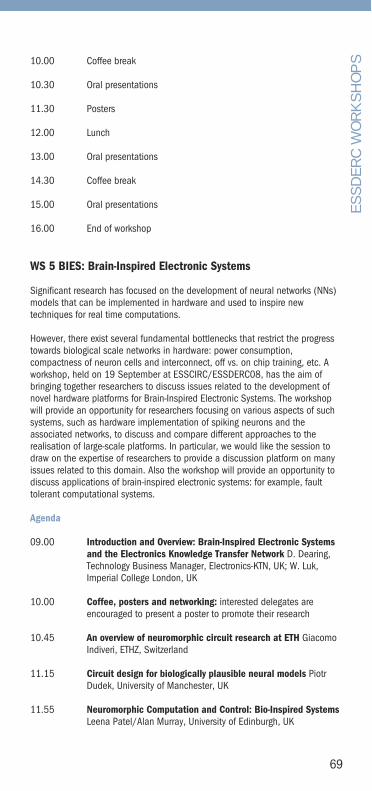
69
ES
SD
ER
C W
OR
KS
HO
PS10.00 Coffee break
10.30 Oral presentations
11.30 Posters
12.00 Lunch
13.00 Oral presentations
14.30 Coffee break
15.00 Oral presentations
16.00 End of workshop
WS 5 BIES: Brain-Inspired Electronic Systems
Significant research has focused on the development of neural networks (NNs)models that can be implemented in hardware and used to inspire newtechniques for real time computations.
However, there exist several fundamental bottlenecks that restrict the progresstowards biological scale networks in hardware: power consumption,compactness of neuron cells and interconnect, off vs. on chip training, etc. Aworkshop, held on 19 September at ESSCIRC/ESSDERC08, has the aim ofbringing together researchers to discuss issues related to the development ofnovel hardware platforms for Brain-Inspired Electronic Systems. The workshopwill provide an opportunity for researchers focusing on various aspects of suchsystems, such as hardware implementation of spiking neurons and theassociated networks, to discuss and compare different approaches to therealisation of large-scale platforms. In particular, we would like the session todraw on the expertise of researchers to provide a discussion platform on manyissues related to this domain. Also the workshop will provide an opportunity todiscuss applications of brain-inspired electronic systems: for example, faulttolerant computational systems.
Agenda
09.00 Introduction and Overview: Brain-Inspired Electronic Systemsand the Electronics Knowledge Transfer Network D. Dearing,Technology Business Manager, Electronics-KTN, UK; W. Luk,Imperial College London, UK
10.00 Coffee, posters and networking: interested delegates are encouraged to present a poster to promote their research
10.45 An overview of neuromorphic circuit research at ETH GiacomoIndiveri, ETHZ, Switzerland
11.15 Circuit design for biologically plausible neural models PiotrDudek, University of Manchester, UK
11.55 Neuromorphic Computation and Control: Bio-Inspired SystemsLeena Patel/Alan Murray, University of Edinburgh, UK

70
ES
SD
ER
C W
OR
KS
HO
PS 12.15 Networking lunch
13.30 Abstracting Both Architecture and Time: The SpiNNakerNeuromimetic Modelling Platform A. Rast, S. Furber, D. Lester,S. Temple, L. Plana, E. Painkras, M. Khan, J. Wu, Y. Shi, S. Yangand X. Jin, University of Manchester, UK
14.00 EMBRACE: A Programmable Hardware Platform for SpikingNeural Networks S. Hall (University of Liverpool), L. McDaid, J.Harkin (Ulster), P. Dudek (Manchester) and L. Smith(Sterling)
14.30 Workshop breakout session facilitated by partner organisationsand aimed at identifying themes and research projects includingthose of use to industry
15.30 Feedback session and discussion – nominated speakers fromeach of the workgroups present the outcomes; followed by opendiscussion
16.00 Coffee
16.15 Summary and follow-up Daniel Dearing, eKTN
Networking and close
WS 6 Si-based Nanodevices for ultimate CMOS and beyond-CMOS
This workshop aims to establish a discussion forum in the field ofnanoelectronics devices. It is supported by the SINANO Institute, which is a newEuropean entity founded by the main laboratories of the European academiccommunity working in this field, and by the European Network of ExcellenceNANOSIL devoted to Silicon-based Nanodevices funded by the EuropeanCommission for the 7th Framework Programme.
Over the next quarter-century, considerable challenges exist to push the limits ofsilicon integration down to nanometric dimensions and to enhance deviceperformance in order to meet the ever increasing demands of communicationand computing. The aim of the workshop is to present the status and trends ofCMOS and beyond-CMOS nanodevices for terascale ICs.
9.00 New Channel Materials for Ultimate CMOS Siegfried Mantl,Institut für Bio- und Nanosysteme, Forschungszentrum Juelich
9.30 Innovative Device Architectures Nanoscale CMOS Nadine Collaert, IMEC
10.00 Refreshment break
10.30 Comparative Analysis of Stress-Induced PerformanceEnhancement in NMOS and PMOS Transistors David Esseni,Udine University
11.00 Characterisation Methods for Nanodevices Sorin Cristoloveanu,IMEP
71
ES
SD
ER
C W
OR
KS
HO
PS11.30 Emerging Nanotechnology for Integration of Nanostructures in
Nanoelectronic Devices Thierry Baron, LTM
12.00 Lunch
13.30 Small Slope Switches Adrian Ionescu, EPFL14.00 3D Multichannels and Stacked Nanowires Technologies
Thomas Ernst, LETI
14.30 Carbon Nanotube – Silicon Heterojunctions forNanoelectronics and Nanosensors Jimmy Xu, Brown University
15.00 Atomic Functionalities in Silicon Devices: Go Beyond the FETby Using Single Dopants and Artificial Silicon Atoms MarcSanquer, INAC
15.30 End of workshop

72
ES
SD
ER
C F
RIN
GE
The Edinburgh fringe will be held in the exhibition, which is situated n theCromdale Hall. This session will take place during the afternoon coffee break onTuesday 16 September 2008. Please refer to the timetable (p6) for furtherdetails. Presenters will also be on hand to discuss their posters outside thistimeslot by prior arrangement. Please come to the registration desk to arrangean alternative session time.
P1 A Micromachined Three-Axis Acceleration Sensor for theMeasurement of Heart Wall MotionCraig Lowrie, Heriot Watt University, UK
P2 On the Design of an Integrated Monolithic 3-AxisPiezoresistive Accelerometer on SOIDr Aboubacar Chaehoi, Institute for System Level Integration, UK
P3 Characterization of Binary Oxide Thin Films Regarding theResistive Switching Effect for the Application in Future HighDensity Non-Volatile MemoriesDr Carsten Kuegeler, Centre of Nanoelectronic Systems forInformation Technology, Germany
P4 Review of the Development of Microscale MagneticComponents for DC-DC Power ConvertersDr David Flynn, Heriot Watt Uiversity, UK
P5 Analysis of the Band-to-Band Tunneling Effect in 65 nm nFETsDr Emmanuel Torres-Rios, INAOE, Mexico
P6 Photoelectric Methods to Determine Distributions ofParameter Values over the Gate Area of MOS DevicesDr Krzysztof Piskorski, Institute of Electron Technology, Poland
P7 Device Process Simulation for EEPROM Cell: Well Optimizationfor HV DevicesDipL-Ing Gerard Dubois, Altissemiconductor, France
P8 Confined and Guided Catalytic Growth of Crystalline SiliconFilms on a Dielectric SubstrateMiss Aurélie Lecestre, IEMN-UMR CNRS/STMicroelctronics,France
P9 Postponing SoC DeathMr Ahmed AbdelHamid, Technology Aware Design, Belgium
P10 Statistical Simulations of High-K-Based Non-Volatile MemoryDevicesMr Andrea Padovani, Universita di Ferrara/IU.NET, Italy
P11 Impact of the Field Induced Polarization Space-Charge on theCharacteristics of AlGaN/GaN HEMT: Self-ConsistentSimulation StudyMr Daniel Balaz, University of Glasgow, UK
ESSDERC fringe
73
ES
SD
ER
C F
RIN
GE
P12 Charge Trapping Properties of Sputtered Hafnium Oxide Filmson Silicon Dioxide Mr Emanuele Verrelli, National Technical University of Athens,Greece
P13 Field-plate LDMOS Devices for RF ApplicationsMr I Cortes, LAAS-CNRS; Universite de Toulouse, France
P14 Interfacing Continuous and Particular Ion TransportTechniques in Nano-Bio Electronic SimulationsMr Iain Moore, University of Glasgow
P15 Layout Dependency of PMOS off Current Degradation due toOff-State StressMr Jae Seo, Samsung Electronics, Korea
P16 BTI and Dielectric Breakdown in High-k Gated NMOSTransistors Studied using DC and Fast MeasurementsMr Juan Boix, Universitat Autonoma di Barcelona, Spain
P17 Study of Apparent Ballistic Magnetoresistance Mobility inNanometer Scale MOSFETsMr Karim Huet, Universite Paris Sud, CNRS/STMicroelectronics,France
P18 Impact of Oxide Progressive Soft Breakdown on MOS DevicesOperation: Experiment and ModelingMr Louis Gerrer, IMEP-LAHC, France
P19 Suspended Gate Silicon Nanodot MemoryMr Mario Garcia-Remirez, University of Southampton, UK
P20 High quality Schottky Contacts for Limiting Leakage Currentsin Ge Based Schottky Barrier MOSFETsMr Muhammad Husain, University of Southampton, UK
P21 Investigation of Strain Profile Optimization in Gate-All-AroundSuspended Silicon Nanowire FETMr Mohammad Najmzadeh, Swill Federal Institute of Technologyin Lausanne (EPFL), Switzerland
P22 Fabrication of Three-Dimensional Inverters Using the u-CzochralskiMr Mohammad Tajari Mofrad, Delft University of Technology,Netherlands
P23 Numerical Simulation of Quasi-Ballistic Transport in Fully-Depleted SOI and Double-Gate MOSFETs: Application to theAnalysis of Circuit PerformancesMr Sébastien Martinie, CEA-LETI MINATEC/IM2NP-CNRS, UMRCNRS 6242
P24 An Axonal Delay Scheme for Spiking Neural NetworksMr Thomas Dowrick, University of Liverpool, UK
P25 SWCNT-MWCNT Crossed Junction by Two-Step
74
ES
SD
ER
C F
RIN
GE Dielectrophoresis
Ms Anupama Arun, Nanolab, EPFL, Switzerland
P26 From Process to Device: Modelling Ultra-shallow Sb Implantsin Strained SiliconMs Yan Lai, Tyndall National Institute, Ireland
P27 An Improved Self-consistent Method and Hole Mobility in Geand GaAs Bulk PMOSFETMs Yan Zhang, University of Massachusetts, USA
P28 Positive Charge Trapping Induced by Plasma Charging Damagein NMOS TransistorsDipL-Ing Sebastian Sommer, Fraunhofer Institut furMikroelektronische Schaltungen und Systeme Duisburg, Germany
P29 A Proposed Wide Input Linear Range OTA CircuitMr Saad Hasan, University of Liverpool, UK
P30 High Efficiency Synchronous Buck Converter using optimisedSplit-Gate RSO MOSFETMr Chin Tong, University of Warwick, UK
P31 Full 3D Real-Space NEGF Simulation of Transport andMagnetotransport in Si-Nanowire FETsMr Claudio Buran, IMEP-LAHC MINATEC, France
P32 A High Output Impedance Current Source for Wideband Bio-Impedance MeasurementsMr Hongwei Hong, University College London, UK
P33 Advanced GeOI structures: from Material Properties to HighPerformance pMOSFETSMr Willliam Van Den Daele, IMEP-LAHC Grenoble – INP MINATECGrenoble, France
P34 Stem Cell Studies Using Micro and NanostructuresMr Aamer Shabbir, Heriot Watt University, UK
P35 Micro-Peltier Devices for BioMEMS ApplicationsMiss Alice Daniels, Heriot Watt University
P36 DNA Nanotechnology Based Biosensors for Rapid DiseaseDiagnosticsWenxing Wang, Heriot Watt University, UK
P37 Stochastic Piecewise Modelling of Post-BD Gate CurrentOriented to Circuit DesignMr Javier Martin-Martinez, Universitat Autonoma di Barcelona,Spain/IMEC, Belgium
P38 Operation and Electrical Quenching of Electroluminescence inMulticolor Eu Doped Metal-Oxide-Silicon Light-Emitting DeviceStanislav Tyagulskiy, Lashkaryov Institute of SemiconductorPhysics, National Academy of Sciences of Ukraine

NO
TES
75
Notes