Embed Size (px)
Citation preview

This document is downloaded from DR‑NTU (https://dr.ntu.edu.sg)Nanyang Technological University, Singapore.
SPP/LSP coupled hybrid mode directedmulti‑functional surface‑enhanced Raman system
Du, Luping
2012
Du, L. (2012). SPP/LSP coupled hybrid mode directed multi‑functional surface‑enhancedRaman system. Doctoral thesis, Nanyang Technological University, Singapore.
https://hdl.handle.net/10356/53455
https://doi.org/10.32657/10356/53455
Downloaded on 26 Jan 2022 18:08:31 SGT

SPP/LSP COUPLED HYBRID MODE DIRECTED
MULTI-FUNCTIONAL SURFACE-ENHANCED
RAMAN SYSTEM
DU LUPING
SCHOOL OF ELECTRICAL & ELECTRONIC ENGINEERING
NANYANG TECHNOLOGICAL UNIVERSITY
2012

SPP/LSP coupled hybrid mode directed
multi-functional surface-enhanced
Raman system
Du Luping
School of Electrical & Electronic Engineering
A thesis submitted to the Nanyang Technological University
in fulfillment of the requirement for the degree of
Doctor of Philosophy
2012

I
Acknowledgement
As with any research project, there are lots of people who contributed to the
completion of my research work as a postgraduate student.
Firstly, I would like to express my appreciation to Professor Yuan Xiaocong for
his support, trust and prudent advice. There are many critical lessons that I learned
from him as a thesis advisor, foremost being the importance of adopting a strategic
approach in research and to always keep the objective in focus. My gratitude also
goes to Associate Professor Tang Dingyuan, who supervised my research work during
my later PhD studies and provided kind support and strategic suggestions.
My sincere thanks go to Associate Professor Zhang Daohua and Associate
Professor Mei Ting. They along with Professor Yuan have generously shared their
wealth of accumulated knowledge whenever I approached them. Their passion was
instrumental in inspiring me to pursue a career in research.
I would also like to thank Dr Yuan Guanghui, Dr Wang Qian, Dr Zhang Ning,
Dr Tan Piausiong, Dr Zhang Duoguo and Dr Moh. K. J. Jonathan. They gave
indispensable help in crucial areas and were an excellent team to work with. My
thanks also go to Ms Yvonne Yang, the support staff of the Photonics Laboratory,
whose years of experience often made resolving technical problems seemingly easier
than they actually were.
Finally, I would like to thank my family members, for their constant
encouragement and emotional support.

II
To Zhang Xi and Our Parents.

III
Table of Contents
ACKNOWLEDGEMENT ............................................................................................. I
TABLE OF CONTENTS ............................................................................................. III
ABSTRACT ............................................................................................................... VII
LIST OF FIGURES ...................................................................................................... X
SYMBOLS AND ABBREVIATIONS ................................................................... XXIV
CHAPTER 1 INTRODUCTION ............................................................................... 1
1.1 MOTIVATION ................................................................................................... 1
1.2 OBJECTIVE ..................................................................................................... 5
1.3 MAJOR ACHIEVEMENTS .................................................................................. 6
1.4 ORGANIZATION OF THIS THESIS...................................................................... 8
CHAPTER 2 LITERATURE REVIEW .................................................................... 9
2.1 SURFACE PLASMONS ...................................................................................... 9
2.1.1 Surface Plasmon Polaritons ............................................................... 11
2.1.2 Localized Surface Plasmon ............................................................... 19
2.1.3 Plasmon Hybridization ...................................................................... 23
2.2 SURFACE-ENHANCED RAMAN SCATTERING .................................................. 27
2.2.1 Raman Enhancement ......................................................................... 28
2.2.2 SERS Substrates ................................................................................ 30

IV
2.3 RADIAL POLARIZATION ................................................................................ 42
2.3.1 Beam Profile ...................................................................................... 42
2.3.2 Full p-polarized Beam ....................................................................... 43
2.3.3 SPPs Excitation Source ..................................................................... 45
CHAPTER 3 SURFACE PLASMON COUPLING MODE – NUMERICAL
INVESTIGATION ....................................................................................................... 47
3.1 CHAPTER INTRODUCTION ............................................................................. 47
3.2 SURFACE PLASMON COUPLING MODE INDUCED BY PERIODIC METALLIC
STRUCTURE ......................................................................................................... 49
3.2.1 Structure ............................................................................................ 49
3.2.2 Simulation Results ............................................................................. 50
3.2.3 Summary ........................................................................................... 56
3.3 SURFACE PLASMON COUPLING MODE INDUCED BY A TIGHTLY-FOCUSED
RADIALLY-POLARIZED BEAM .............................................................................. 57
3.3.1 Excitation Configuration ................................................................... 57
3.3.2 Generation of Radial Polarization Numerically ................................ 58
3.3.3 Realization of Tight Focus Numerically ........................................... 60
3.3.4 Simulation Results ............................................................................. 61
3.3.5 Discussion ......................................................................................... 67
3.3.6 Summary ........................................................................................... 69
CHAPTER 4 SURFACE PLASMON COUPLING MODE FOR SERS ................ 70

V
4.1 CHAPTER INTRODUCTION ............................................................................. 70
4.2 GENERATION OF A RP BEAM EXPERIMENTALLY ........................................... 71
4.3 NANOSPHERE SUB-MONOLAYER ................................................................... 74
4.3.1 Experimental Setup and Procedures .................................................. 74
4.3.2 Experimental Results and Discussion ............................................... 75
4.3.3 Summary ........................................................................................... 81
4.4 SINGLE NANOSPHERE ................................................................................... 82
4.4.1 Surface Plasmon Virtual Probe .......................................................... 82
4.4.2 Experimental Results ......................................................................... 85
4.4.3 Evaluation of Raman Enhancement .................................................. 87
4.4.4 Summary ........................................................................................... 89
CHAPTER 5 DIRECTIONAL EMISSION OF SERS ............................................ 90
5.1 CHAPTER INTRODUCTION ............................................................................. 90
5.2 MECHANISM ................................................................................................. 91
5.3 RESULTS ....................................................................................................... 95
5.3.1 Fourier Plane ..................................................................................... 95
5.3.2 Image Plane ....................................................................................... 98
5.4 DISCUSSION ................................................................................................ 102
5.5 SUMMARY .................................................................................................. 105
CHAPTER 6 SPP-LONGITUDINAL-COMPONENT DETECTION WITH SERS
IMAGING 106

VI
6.1 CHAPTER INTRODUCTION ........................................................................... 106
6.2 PRINCIPLE .................................................................................................. 108
6.3 MAPPING SPP FIELDS WITH SERS IMAGING .............................................. 109
6.4 NUMERICAL-MODELLING WITH FDTD METHOD ....................................... 114
6.5 SUMMARY .................................................................................................. 117
CHAPTER 7 CONCLUSIONS AND FUTURE WORKS .................................... 120
7.1 CONCLUSIONS ............................................................................................ 120
7.2 FUTURE WORKS ......................................................................................... 122
7.2.1 Surface Plasmon Virtual Probe Directed Tip-enhanced Raman
Spectroscopy ................................................................................... 122
7.2.2 All-in-one Surface & Tip-enhanced Raman System ....................... 125
AUTHORS PUBLICATIONS ................................................................................... 128
REFERENCES .......................................................................................................... 129

VII
Abstract
Surface plasmons (SPs) have generated a tremendous amount of interest in recent
decades due to their intriguing features such as lateral spatial confinement, surface
sensitivity and field enhancement. The consistent investigation of SPs leads to a wide
scope of applications including ultrahigh-sensitivity biosensing, super-resolution
imaging, sub-wavelength nanolithography, miniaturized photonic circuits, surface-
enhanced Raman spectroscopy (SERS), etc.
In this thesis, a multi-functional surface-enhanced Raman system based on the
SP-hybrid-mode is proposed and investigated. The system is grounded on a novel idea,
which utilizes the giant electromagnetic enhancement arising from the strong coupling
between surface plasmon polaritons (SPPs) and localized surface plasmon (LSP), the
two different types of SP modes, and deals with the problems facing with SERS and
other SP-based techniques.
First of all, as a fundamental investigation, two types of excitation configurations
are proposed to achieve the plasmon-hybrid-mode: through a periodic metallic
structure and via an attenuated total reflection configuration, respectively. In both
approaches, the numerical investigation with three-dimensional finite-difference
time-domain method shows that the coupling between the LSP and SPPs could result
in a great improvement of electromagnetic enhancement compared to that from
separate SP mode. Raman enhancement of more than 109 was predicted from the
numerical simulation.
SERS experiment was carried out afterwards to verify the Raman enhancement.
In the experiment, SPPs are excited by a tightly-focused radially polarized beam and
interact with the nanospheres to generate the plasmon-hybrid-mode, exactly according
to the second configuration aforementioned. The experimental result demonstrates
VIII
that silver nanospheres within the propagation region of SPPs are effectively activated
and detected by a CCD camera. Raman enhancement presents 20 times improvement
compared to the conventional nanoparticle-induced SPPs/LSP co-enhanced Raman
spectroscopy. Surface-enhanced Raman scattering (also termed as SERS) from single
nanosphere-film junction is realized, which is of significance for SERS as a
quantitative analytical tool. It is also the basis for the following experimental work.
Subsequently, surface plasmon coupled-emission (SPCE) of SERS was studied.
It is found that Raman signal originated from molecules sitting at the nanosphere-film
junction can couple back to SPPs, and eventually radiates into the substrate side with
high refractive index at SPP resonant angles. Collection efficiency of SERS can be
improved with the help of SPCE. Meanwhile, due to the extremely narrow linewidth
of Raman peaks, the SPCE curve of SERS can also be employed for measuring the
propagation length of SPPs and quantitatively characterizing the point spread function
of an SPCE microscopy.
Last but not least, as a promising application, the two-dimensional mapping of
the strongly-dominant longitudinal field component of SPPs was realized based on the
SERS imaging. Our method takes advantage of SERS from a single nanosphere-film
junction where the enhancement factor is determined by the longitudinal component
of coupled SPPs between the nanosphere and metal film. By scanning the nanosphere
immobilized on the film over the propagation region of SPPs, We can map out the
near-field SPP longitudinal field with super-resolution.
To sum up, a plasmon-hybrid-mode directed surface-enhanced Raman system is
proposed in this thesis. By utilizing the coupling-effect between SPPs and LSP,
Raman enhancement of more than 109 was predicted numerically and more than 10
8
was achieved experimentally. Moreover, collection efficiency of SERS originating

IX
from the nanosphere-film junctions can also be improved because of the plasmon
hybridization. Finally, our system can also serve as a powerful SPP-characterization
tool, for measuring the propagation length and mapping the near-field profiles and
dynamics of SPPs.

X
List of Figures
Fig.2.1. Schematic diagrams illustrating a surface plasmon polariton (a) and
localized surface plasmon (b), respectively [48]. ........................................ 10
Fig.2.2. Single dielectric-metal interface for SPPs excitation and propagation. ...... 11
Fig.2.3. Permittivities of silver and gold over the visible spectrum. Ref. [50] ......... 13
Fig.2.4 Dispersion relations of free space photons (A), free photons propagating in
dielectric (B) and the surface plasmons (C). ................................................ 14
Fig.2.5 ATR couplers for SPPs excitation. (a) The Otto configuration, (b) the
Kretschmann-Raether configuration and (c) the objective configuration,
respectively. Ref. [51] .................................................................................. 15
Fig.2.6 Schematic of launching SPPs by a near-field tapered fiber probe (a) or a
scatterer (b). Ref. [51] .................................................................................. 16
Fig.2.7 SPPs excitation based on grating configuration. Ref. [51] ........................... 17
Fig.2.8 The scheme of a leakage radiation microscopy ............................................ 18
Fig.2.9. (a) Schematic of a sphere-shaped noble metal NP interacts with a
uniformly-distributed electromagnetic radiation. (b) Contour map of the
electric field distribution of a dipole mode. ................................................. 20
Fig.2.10. LSP excitation on an individual silver NP of different shapes. Ref. [9, 13] . 22
Fig.2.11. Demonstration of the LSP-LSP hybridization. (a) LSP mode excited on an
individual NP. (b) LSP-LSP hybridization on a NP-NP junction
configuration. The Coulomb interaction between the NPs leads to an energy

XI
splitting of the plasmon-hybridized modes. Ref. [79] ................................. 23
Fig.2.12. Electromagnetic enhancement from LSP-LSP hybridization. Ref. [13] ...... 24
Fig.2.13. Demonstration of the LSP-SPP hybridization. (a) A typical example of a
two-dimensional periodic metallic structure supporting the LSP-SPP
hybridization, in which LSP is excited on each of the metallic NPs while
SPPs spreading all over the space between the NPs. (b) Dispersion diagram
of a two-dimensional periodic metallic structure. Energy splitting occurs
when SPP and LSP are excited simultaneously. Ref. [82-83] ...................... 25
Fig.2.14. NP-film junction induced plasmon hybridization. (a) Simplified
representation of a plasmonic NP interaction with a gold film. The dipole
parallel to the gold film is canceled out by the induced image dipole. (b)
The dipole perpendicular to the gold film resonantly couples to the induced
image dipole, and scatters into the far-field. (c) and (d) Experimentally
observed far-field scattering from a 60 nm gold NP on a 45 nm gold film
illuminated with polarization parallel (scattering is damped and is virtually
undetectable) and perpendicular to the film (which couples to the vertically
oriented dipole and is scattered into the far-field), respectively. (e) Color
image and typical spectrum of 60 nm gold NPs in a quasi-uniform dielectric
(at a glass-H2O interface) and (f) on the surface of the 45 nm thick planar
gold film (under dark-field illumination), which shows a red-shift of
resonant wavelength..................................................................................... 26

XII
Fig.2.15. Electromagnetic enhancement induced by the LSP-SPP hybridization.
Electric field is significantly confined within the NP-film gap. Ref. [37, 84]
...................................................................................................................... 27
Fig.2.16. Roughened electrodes as a SERS substrate formed by means of EC-ORC.
Ref. [3] ......................................................................................................... 31
Fig.2.17. chemically-synthesized metallic NPs with different shapes. (a): nanospheres,
(b): nanocubes, (c): nanotriangles, (d): nanorods, (e): nanorices and (f):
nanobeams. Ref. [119, 121] ......................................................................... 32
Fig.2.18. Highly ordered NPs formed by means of chemical assembly method. Ref.
[112] ............................................................................................................. 34
Fig.2.19. Highly ordered NPs formed by means of Langmuir Blodgett method. Ref.
[131] ............................................................................................................. 35
Fig.2.20. (a) Illustration of the process of NSL. (b) AFM image of an NSL-fabricated
NP array in which the nanosphere mask has been removed. (c) AFM image
of a film-over-nanosphere substrate in which the nanospheres remain on the
surface. Ref. [48].......................................................................................... 36
Fig.2.21. Highly ordered NPs formed by means of nanolithography method. Ref. [137]
...................................................................................................................... 37
Fig.2.22. SERS substrates of metallic NP cluster with inter-particle junction. (a):
dimer and (b): trimer. ................................................................................... 38
Fig.2.23. Inter-particle junction created by optical trapping technique and employed

XIII
for SERS. (a) SERS spectrum from a single immobilized particle (I) shows
no signal. (b) An optically trapped particle (T), without SERS signal, is
moved toward the immobilized one. (c) When brought into near-field
contact, the particle pair (P) shows a strongly enhanced SERS signal. Ref.
[16] ............................................................................................................... 39
Fig.2.24. NP-film junction as SERS substrate, which presents remarkable
reproducibility as well as high Raman enhancement. Ref. [27] .................. 40
Fig.2.25. Double-resonance SERS substrate with LSP-LSP interaction. (a) Schematic
illustration of the structure. (b) Simulated extinction (solid line) and
near-field intensity (dashed line) spectra. Near-field intensity spectrum
shows intensity enhancement at a monitor point on the rod as a function of
illumination wavelength. Near-field spectrum exhibits two pronounced
resonances at λ = 733 and 798 nm. (c) Normalized field distribution, |E|, for
illumination at λ = 733 nm and (d) for illumination at λ= 798 nm. (e)
Carefully designed substrate with resonant wavelengths match the
excitation wavelength and one of the Raman peak. (f) The improvement of
Raman signal for the selected Raman peak. Ref. [145] ............................... 41
Fig.2.26. Double-resonance SERS substrate with LSP-SPP interaction. (a) Schematic
and SEM image of the substrate. (b) Extinction cross-section and SERS
spectrum of array with period of 780 nm. Dashed line illustrates the
excitation wavelength. Ref. [147] ................................................................ 42

XIV
Fig.2.27. Beam shapes of a linearly polarized gaussian beam (a) and a radially
polarized beam (b), respectively. (c) The corresponding amplitude
distributions. The white arrows indicate the direction of light polarizations.
...................................................................................................................... 43
Fig.2.28. Comparison of the focusing properties of a linearly, radially and azimuthally
polarized beam. ............................................................................................ 44
Fig.2.29. (a) Diagram of SPP excitation with highly focused RP beam. (b) Back
Fourier plane image of the reflected beam, in which an axis-symmetric dark
ring is observed that is due to the SPPs excitation. Ref. [40] ...................... 45
Fig.2.30. Calculated SP intensity distribution at silver/air interface with radially
polarized illumination. (a) Total intensity |E|2; (b) longitudinal component
|Ez|2; (c) Radial component |Er|
2; (d) |∇Ez|
2 distribution, which is
proportional to the NSOM signal detected by an apertured fiber probe. Ref.
[40] ............................................................................................................... 46
Fig.3.1. Schematic of the proposed structure and its cross-sectional view along the
dashed line. .................................................................................................. 49
Fig.3.2. Absorption spectra based on: semi-infinite water-silver flat interface
configuration (dashed line), 40-nm-thick silver film sandwiched between
water and Si configuration (dotted line), and dielectric grating covered by
40-nm-thick silver film configuration (solid line). ...................................... 51
Fig.3.3. |E|2 distributions at the top of cubic bumps along XY plane at various

XV
resonant conditions, i.e., the incident wavelength of (a) 450 nm
corresponding to the high order LSP, (b) 637 nm to the SPP, and (c) 670 nm
to the first-order LSP. The colorbar scale is set as log10(|E|2). ..................... 53
Fig.3.4. (a) Absorption spectra for various periods from 426 nm to 546 nm with a 24
nm increment; (b) absorption peak positions versus different periods for
LSP (circles) and SPP (squares), with corresponding maximum local |E| at
resonant wavelength of SPP (triangles). The silver film thickness is 40 nm,
the bump height is 100 nm and the environment is water. .......................... 54
Fig.3.5. Absorption peak positions at various silver film thicknesses for LSP (circles)
and SPP (squares), as well as the corresponding maximum local |E| at
resonant wavelengths of SPP (triangles). The structural period is fixed at
475 nm, the bump height is 100 nm and the environment is water. ............ 55
Fig.3.6. |E|2 distributions under surface plasmon coupling conditions in Fig.3.4 (b)
(left), and in Fig.3.5 (right), respectively. The colorbar scale is set as
log10(|E|2). ..................................................................................................... 56
Fig.3.7. Proposed optical configuration through a high NA objective lens for
plasmon-hybrid-mode, in which a RP light is tightly focused onto a
silver-air interface to excite SPPs, which subsequently interact with a silver
nanosphere on top of the silver film to excite LSP. ..................................... 57
Fig.3.8. Phases imposed onto a right-handed (a) and a left-handed circularly
polarized light (b), respectively, to achieve a RP beam. .............................. 59

XVI
Fig.3.9. Input (a) and output (b) amplitude distributions of a RP light. ................... 59
Fig.3.10. Illustration of a tightly-focused RP light realized by setting an initial
equivalent phase function of lens in the source file; 1: the focal point of the
system, which is determined by the phase function of lens; 2: indication of
the excitation of SPPs from all directions; 3: convergence verification of the
simulation to ensure the accuracy. ............................................................... 61
Fig.3.11. |Ez| distribution at XZ plane calculated by 3D-FDTD (contour map) and by
Richard-Wolf diffraction theory (solid curve), for comparison. The results
accord well with each other. ......................................................................... 62
Fig.3.12. Transmission of a 45-nm-thick silver film sandwiched by semi-infinite air
(n=1) and glass (n=1.515), obtained with the transfer matrix method. ....... 63
Fig.3.13. (a) Contour map of electric energy density around the nanosphere at a 532
nm incident wavelength excitation. (b) Exponential-decay-fitting of the
electric energy density in the vicinity of the nanosphere-film junction along
the dashed red line as illustrated with the inset. ........................................... 64
Fig.3.14. Enhanced electric fields at various incident wavelengths ranging from 380
nm to 560 nm for the proposed (blue line) and controlled configurations
(red line), respectively. ................................................................................. 65
Fig.3.15. Electric field distributions under resonant wavelengths for the cases of
45-nm-thick silver film (a) and 45-nm-thick glass film (b), respectively. The
unit for x and y axis is m and the scale bar is set as log10(|E|2). ................ 66

XVII
Fig.3.16. Demonstration of the NP-driven (a) and film-driven (b) plasmon-hybridized
gap mode. ..................................................................................................... 67
Fig.3.17. Transversal (left) and longitudinal (right) electric field distributions at the
focal plane under a tightly-focused linearly polarized Gaussian beam.
NA=0.98. The smaller the NA, the stronger (weaker) the transversal
(longitudinal) field component. ................................................................... 68
Fig.4.1. Generation and verification of a RP beam experimentally. (a) Illustration of
an optical configuration transferring a linearly polarized Gaussian beam into
a RP beam. LP: linear polarizer, QW: quarter waveplate, AA:
azimuthal-type analyzer, SPE: spiral phase element, HW; half waveplate. (b)
Schematic view of an SPE and a real one. (c) Transmission axis of an
azimuthal-type analyzer. (d) Verification of a RP beam by using a linear
polarizer........................................................................................................ 72
Fig.4.2. Optical schematic of a plasmon-hybrid-mode based surface-enhanced
Raman spectroscopy. A 532nm RP beam is used as the illumination. ......... 74
Fig.4.3. Dark-field image of immobilized silver nanospheres on a 45-nm-thick silver
film. .............................................................................................................. 75
Fig.4.4. Raman images of silver nanospheres immobilized on a silver film surface at
various sample-objective lens distances obtained by a CCD camera (a-i),
and the corresponding types of excitation schemes. (j): post-focal plane, (k):
on-focal plane and (l): pro-focal plane schemes. ......................................... 77

XVIII
Fig.4.5. Raman images of silver nanospheres obtained by a CCD camera when the
sample locates exactly at the focal plane of the objective lens, with (a) and
without (b) the SPPs excitation. (c) Demonstration of on-focal plane
excitation scheme, under which incident beam is focused onto the interface
into a minimum spot. (d) Reflected laser beam obtained at the back Fourier
plane. The sharp dark ring represents a reflectivity dip thus indicating the
SPPs excitation at the silver-air interface. ................................................... 78
Fig.4.6. Raman spectra of R6G molecules at various RP beam sizes, with a-f
representing the increase of beam size. Laser power incident onto the
sample is approximately 500 μW. Integration time of 1 second was used to
collect the Raman signals............................................................................. 80
Fig.4.7. Dark-field image of silver nanospheres with much lower density
immobilized on a silver surface. The yellow scale bar represents 5 m. .... 82
Fig.4.8. Longitudinal electric field distribution in the vicinity of the focus for a
radially-polarized (a) and a linearly-polarized Gaussian beam (b),
respectively. (c) Electric field distribution around the silver nanosphere as it
locates at the center of SP-VP. ..................................................................... 83
Fig.4.9. SERS spectra of 4-mba molecules from single nanosphere-film junction
located at the center of SP-VP (Black) and without the excitation of SPPs
(Red), respectively. The inset presents the simultaneously captured Raman
image of an individual silver nanosphere, with SPPs excitation. ................ 85

XIX
Fig.4.10. Normalized Raman intensity from individual NP-film junction as it was
scanned over the SP-VP region, plotting against the transversal axis (Line
with stars), and the electric field distribution of an SP-VP obtained
numerically by Richard-Wolf vectorial diffraction method (Line only). ..... 86
Fig.5.1. (a) Schematic view of the experimenetal setup investigating the SPCE of
SERS from single nanosphere–film juncion. (b) SERS spectrum of 4-mba
molecules adsorbed at the junction. ............................................................. 91
Fig.5.2. Three-layer system for the Fresnel coefficients calculation ........................ 92
Fig.5.3. Transmission features of the three-layer system under different
circumstances. (a) Calculated transmittance plots against the incident angle
(3) when incident light illuminates from glass into air. (b) and (c) The
transmittance plots against the incident angle (1) and transmitted angle (3),
respectively, when incident light illuminates from air into glass. Wavelength
is set to be 532 nm in the calculation. .......................................................... 93
Fig.5.4. (a) Transmission coefficients of a 55-nm-thick silver film sandwiched by
semi-infinite air and glass under 564 nm, 573 nm, and 581 nm incident
wavelengths, respectively. The wavelengths are corresponding to the three
main Raman peaks of 4-mba molecules. (b) Back Fourier plane image of
SERS from 4-mba molecules. The coupled-emission of SERS forms the
colorful SPCE ring. ...................................................................................... 96
Fig.5.5. Pixel intensity distribution along the dashed line as shown in Fig.5.4 (b)

XX
plots against the wave-number derived from the transmitted angle. ........... 97
Fig.5.6 Schematic of the imaging process within a 4f optical system of an SPCE
microscope. .................................................................................................. 99
Fig.5.7. (a) Calculated PSF of an SPCE microscopy. (b) The actual SPCE image of
SERS from 4-mba molecules obtained at the back image plane. (c)
Cross-section distributions across the center of (a) and (b), for the purpose
of comparison............................................................................................. 101
Fig.5.8. PSF of an SPCE microscopy obtained with fluorescence for comparison
[180]. .......................................................................................................... 102
Fig.5.9. Intensity comparison between the Raman signals of R6G molecules
collected at the glass side through SPCE and collected directly at the air
side (conventional). Integration time is 1s. Collection efficiency is shown to
be enhanced through SPCE. ....................................................................... 104
Fig.6.1. Working principe of plasmon-hybridized gap modes directed
characterizaiton of SPPs (a) Field feature of a typical SP-VP excited by a
RP beam, which is essentially an evanescent Bessel-like standing-wave. (b)
Illustration of a nanosphere-film junction interacting with the longitudinal
(“A”) and transversal field (“B”) of an SPP standing wave. The longitudinal
field will drive the harmonic oscillation of free electrons inside the
nanosphere perpendicular to the metal film, leadig to a vertically-oriented
plasmon-hybridized gap mode; while a lateral gap mode will be excited by

XXI
the transversal field. The different schemes of nanosphere/film interaction
will result in an energy splitting of these two kinds of plasmon-hybridized
gap modes. (c) Demonstration of the mode-splitting induced longitudinal
field sensitivity. At specific incident wavelengths, field enhancement
induced by the vertical gap mode is much higher. The enhanced electric
field can be used to excite SERS signal of molecules at the nanosphere-film
gap. Since the vertical gap mode contributes a higher Raman enhancement,
the intensity of SERS can be used to characterize SPPs dominant
longitudinal field. (d) Schematic diagram of plasmon-hybridized gap modes
directed, SERS-based SPPs detection system. Diagram is not to scale. .... 109
Fig.6.2. Mapping an SP-VP with SERS imaging. (a) Measured near-field
distribution of plasmon virtual probe produced by a tightly-focused RP
beam, compared with its calculated longitudinal (b) and transversal (c)
electric field components. (d) Cross-section distribution comparison
between the measured virtual probe and calculated longitudinal field
component. (e) Statistical measurement of the central spot size of plasmon
virtual probe with 50 randomly-selected nanospheres on the metal film,
verifying the accuracy and reproducibility of our measurement. Incident
wavelength is 532nm. Area of contour maps is 4 m 4 m. .................. 110
Fig.6.3 The mapping of SPP patterns under a tightly-focused linearly polarized
Gaussian beam (LPGB), a circularly polarized beam (CPB) and a linearly

XXII
polarized optical-vortex beam (LPVB) of charge “1”, respectively, to verify
further the longitudinal field sensitivity of our method and show the distinct
SPP patterns under different incident polarizations. From top to bottom:
measured, calculated |Ez|2 and calculated |Er|
2, respectively. From left to
right: LPGB, CPB and LPVB, respectively. Area of contour maps is 4 m
4 m. Incident wavelength is 532 nm. ....................................................... 112
Fig.6.4. Comparison of SPPs distribution obtained with NSOM [42, 63, 68] (top)
and our SERS imaging (bottom). From left to right: linearly polarized
Gaussian beam, radially polarized beam, and linearly polarized optical
vortex beam, respectively. .......................................................................... 113
Fig.6.5. Numerical-modelling of a nanosphere-film junction interacting with SP-VP.
(a) Normalized maximum electric field at the nanosphere-film junction
plots against the wavelength, when the nanosphere placed at the standing
wave node (point “A” in Fig.6.1 (b), vertical gap mode), anti-node (point “B”
in Fig.6.1 (b), lateral gap mode), and on a glass substrate, respectively. (b)
and (c) Electric field vectorial distribution in the vicinity of nanosphere-film
gap, in the case of lateral and vertical gap mode, respectively. (d) Calculated
averaged Raman enhancement for each mode, which is employed to
evaluate the field sensitivity of a NP-film junction. Left vertical axis is set
as log10(RE). ............................................................................................... 115
Fig.6.6. Contour maps of electric field distribution. (a) and (b) Vertical and lateral

XXIII
gap mode in the XZ plane. (c) and (d) The corresponding modes in the
nanosphere-film gap plane, respectively. Colorbar scale is set as log10(|E|2).
The arrows represent the electric field orientation of SP-VP in the absence
of nanosphere. Incident wavelength is 532 nm. ......................................... 116
Fig.6.7. Front view of the Labview program coded for two-dimensional mapping of
SPP’s longitudinal component. .................................................................. 119
Fig.7.1. High sensitivity, high resolution tip-enhanced Raman spectroscopy based
on surface plasmon virtual probe and surface plasmon coupled-emission.
.................................................................................................................... 122
Fig.7.2. Controllable vertically-oriented dimer structure based on AFM tip, excited
by an SP-VP ............................................................................................... 124
Fig.7.3. Near-field distribution around a vertically-oriented dimer structure excited
by a surface plasmon virtual probe, with 480 nm incident wavelength. The
white scale bar represents 100 nm. ............................................................ 125
Fig.7.4. Schematic view of an all-in-one surface-enhanced Raman system. HW: half
waveplate; LP: linear polarizer; BS: beam splitter; BFP: back Fourier plane;
IP: image plane; Spec: spectrometer; PC: personal computer; NS:
nanosphere. ................................................................................................ 126

XXIV
Symbols and Abbreviations
List of Symbols
: polarizability
: wave-vector of SPP
ε: permittivity
: potential
: azimuthal angle
: wavelength
θ: incident angle
: cross-section
: transmission coefficient
ω: frequency
Λ: pitch
c: speed of light
d: distance
f: focal length
k: wave-vector
l: angular momentum
m: diffraction order
n: refractive index
r: radial coordinate
t: thickness
w: beam waist
x: x coordinate

XXV
y: y coordinate
z: z coordinate
H: magnetic field
L: propagation length
G: grating constant
R: radius
List of Abbreviations
ATR: attenuated total reflection
BFP: back focal/fourier plane
CCD: charge-coupled device
DDA: discrete dipole approximation
EBL: electron beam lithography
FDTD: finite-difference time-domain
FWHM: full width at half maximum
LSP: localized surface plasmon
NA: numerical aperture
NP: nanoparticle
NSOM: near-field scanning optical microscope
PMT: photomultiplier tubes
PSF: point spread function
PSP: propagating surface plasmon
RP: radially polarized
SERS: surface-enhanced Raman scattering / surface-enhanced Raman spectroscopy
SPs: surface plasmons

XXVI
SPCE: surface plasmon-coupled emission
SPP: surface plasmon polariton
SPR: surface plasmon resonance
TM: transverse magnetic
TE: transverse electric

Chapter 1 Introduction
1
Chapter 1 Introduction
1.1 Motivation
Raman scattering is an inelastic scattering process between a photon and a molecule
[1]. It was firstly observed in 1928 and quickly becoming an important branch of
optical detection techniques due to its unique spectral features. Compared to the
fluorescence of molecules, Raman spectrum is much sharper, with each peak
representing the molecular vibrational or rotational mode, and hence enables the
detection of uniquely identifying molecular fingerprints. However, the cross-section
of Raman scattering is extremely small. It is 12-14 orders of magnitude lower than
typical fluorescence cross-sections [2]. Thus, despite the rich information offered by
regular Raman spectroscopy, it has not been the primary choice as a handy analytical
tool.
The discovery of surface enhanced Raman scattering (SERS) opened a new
avenue for Raman spectroscopy [3]. When molecules are residing at or near specific
metallic nanostructure surface, the Raman scattering cross-sections are hugely
enhanced, rendering them even comparable to that of fluorescence. The large signal
enhancement allows vibrational spectrum to be measured from molecules that would
otherwise be spectroscopically silent. In particular, the observation of single-molecule
SERS by Kneipp, Nie, and their co-workers boosts the development of SERS [2, 4],
and it rapidly becomes a powerful analytical tool for chemical and biological sensing
application.
The enhancement effect plays a crucial role in SERS. Chemical and
electromagnetic enhancement are widely believed the two main contributions, with

Chapter 1 Introduction
2
the latter being the dominant one [5-6]. The electromagnetic enhancement arises from
the light-substrate interaction, which consists of the resonant excitation of surface
plasmon modes (LSP, SPP, or both of them), the lightning rod effect, and the image
field effect [7-8], with SP making the major contribution. The SP frequency and the
induced electromagnetic enhancement are strongly dependent on the incident light
wavelength, polarization, substrate morphology, and environment medium [9-10].
Researchers have made great effort to develop a robust SERS substrate to optimize
the electromagnetic enhancement.
Noble metal nanoparticles (NPs) are the most widely used SERS substrate to
enhance the Raman signals. With the fast development of nano-science and
nano-technology, NPs of different sizes and shapes can easily be synthesized [11].
The electromagnetic enhancement of an individual NP ranges from several tens to
several hundred, depending on its composite and shape [12-14]. In terms of Raman
enhancement, it is on the order of 103 - 10
7. Such Raman enhancement is mainly from
the excitation of LSP and is relatively low among the family of SERS substrates.
As two NPs are put together (dimer configuration), with inter-particle separation
on the order of several nanometers, the electromagnetic enhancement can
substantially be improved [15-19]. This huge enhancement is believed due to the
strong coupling between the LSP modes on each particle (LSP-LSP hybridization).
Single molecule sensitivity has been realized on the dimer structures [20-21].
However, the nature of random formation of inter-particle junction makes it quite
irreproducible, causing Raman enhancement with dramatic variations, often by many
orders of magnitude. This significantly restricts its practical application as a robust
SERS substrate.
An alternative junction is created in a NP-film gap mode system, in which one of

Chapter 1 Introduction
3
the NPs is replaced by a smooth metal film [22-30]. Experimental studies
demonstrated that such NP-film junction configuration is capable of providing
remarkably reproducible SERS-active hotspots compared with the NP-NP junction
[27]. Moreover, due to the coupling between the LSP excited on the NP and the SPPs
generated on the conducting surface (LSP-SPPs hybridization), the electromagnetic
enhancement shows more advantageous than that on a dielectric substrate (such as
glass, silicon or SiO2), in which only LSP is present. The combination of high
reproducibility with high Raman enhancement of NP-film junctions makes them a
great potential as robust SERS substrates. However, in the preceding work regarding
NP-film junction, there exist two main drawbacks.
Firstly, the SPPs formed on the smooth metal surface are induced by the NPs,
which diffract the incident beam, generating the required wave-vector to match that of
SPPs (NP-driven plasmon hybridization). Such an excitation approach is rather
inefficient and hence limiting its Raman enhancement compared with that from
NP-NP junction. Secondly, due to the vertical arrangement of an NP-film junction, an
electric field component oriented vertically (perpendicular to the metal surface; also
called as longitudinal field component) is preferred to efficiently excite an SP
coupling mode at the junction [29, 31-37]. In the preceding SERS experiments,
linearly polarized Gaussian beam was focused directly on to the NP-film junction.
Although longitudinal electric field component does exist under this kind of excitation
approach, it is the subordinate field component and the power utility is therefore quite
low [38-39].
Hence, improving the excitation efficiency of SPPs and meanwhile increasing
the electric field longitudinal component in a NP-film junction based SERS system is
of great significance.

Chapter 1 Introduction
4
Surface plasmon virtual probe (SP-VP) generated by a tightly-focused radially
polarized (RP) beam would be a great candidate as the excitation source for the
aforementioned NP-film junction based SERS system [40]. RP light is a uniquely
polarized light pattern whose distribution of electric field vectors is arranged radially
around the optic axis of a laser beam. When a RP light is tightly-focused onto a
metal-dielectric interface, the entire beam is p-polarized with respective to the
interface, which enables the excitation of SPPs from all azimuthal directions to form
an evanescent Bessel-like standing-wave at the focal region. Such evanescent
standing-wave has a sharply-confined SPP spot at the center of focal plane, with the
longitudinal field component dominating its total electric field [41-43]. The
sharply-confined SPP spot is therefore termed as surface plasmon virtual probe. As a
result, by using the SP-VP as the excitation source, both of the above drawbacks are
overcome, and the NP-film junction configuration therefore can be as a robust SERS
substrate, owing to its high reproducibility and Raman enhancement.
Before we use the SP-VP as the excitation source, it is important to map its
near-field distribution above the metal film, particularly its longitudinal electric field
component. However, there is no experimental technique up to now, which can
effectively map the near-field distribution of SP-VP in the visible range, and hence
verify the formation of it. The difficulty of mapping an SP-VP lies in that: first of all,
due to the evanescent and sub-wavelength nature of SP-VP, the traditional far-field
techniques, such as conventional optical microscopy, lose effectiveness; secondly, the
field of an SP-VP is strongly-dominated by the longitudinal component, which is
largely unmeasurable by near-field scanning optical microscope (NSOM), the most
convenient tool to measure the field distribution of SPPs [42]. As a result, it would be
of great significance if a novel detection technique is developed to efficiently and

Chapter 1 Introduction
5
accurately map the field distribution of SP-VP. An interesting thing is that: since the
SP-VP can be as an optimized source for the excitation of SERS based on the NP-film
junction, the NP-film junction, in turn, can be employed as an SP-antenna to detect
the field distribution of SP-VP by means of SERS imaging. This is the second
motivation of this thesis.
Finally, besides the SPPs contribution on the excitation of SERS signals, recent
experimental work demonstrated that the emitted Raman radiation is also able to
couple back to SPs with periodic metallic structure or nanoantennas, forming a “beam
shaped” Raman scattering”. Such shaped emission of Raman scattering is able to
improve its collection efficiency. Motivated by their work, in this thesis, we
investigate the emission pattern of SERS from single NP-film junction. Because of
the presence of a thin metal film, Raman scattering from the NP-film junction is able
to couple back to SPPs supported at the air-metal interface, and eventually re-radiates
into the substrate side with higher refractive index. The so-call surface plasmon
coupled-emission (SPCE) [44-46] is able to improve the collection efficiency of
SERS, and the SPCE curve of SERS can also be used for measuring the propagation
length of SPPs and the point spread function of an SPCE microscopy.
1.2 Objective
Grounded on the discussion above, the main research focus of this thesis is to develop
a robust SERS substrate based on the plasmon hybridization, which, accompanying
with a suitable excitation source, can provide a relatively high Raman enhancement
with high reproducibility, and extend it to other SPs-based applications. The objective
is divided into three sub-items as following:
(1) From the excitation point of view, SP-VP excited by a tightly-focused RP beam is

Chapter 1 Introduction
6
introduced into the conventional NP-film junction based SERS system to improve
further the Raman enhancement. We will investigate the plasmonic response of the
new excitation scheme both from simulation and experiment, in term of Raman
enhancement.
(2) From the collection point of view, surface plasmon coupled-emission of SERS
from single NP-film junction will be studied. Our investigation of SPCE will
focus on the mechanism, the induced collection efficiency improvement of SERS
and its corresponding applications.
(3) From the characterization point of view, since SP-VP will be employed as the
excitation source in our SERS system, accurately and efficiently mapping its
near-field distribution is essential. As the final objective of the thesis, we propose
a novel technique to detect the near-field distribution of SPPs (including SP-VP),
which is based on the SERS imaging from single NP-film junction. The principle
and performance of our method will be demonstrated.
1.3 Major Achievements
Below presents the major achievements in this thesis:
(a) Localized surface plasmon is excited by a surface plasmon virtual probe
To our best knowledge, it is our original work that LSP is excited by an SP-VP
(film-driven plasmon hybridization), and the induced high electromagnetic
enhancement is employed for SERS. Raman enhancement of more than 1010
was
predicted from the numerical simulation and more than 108 was achieved in the
experiment. The proposed configuration possesses both high Raman enhancement and
reproducibility and hence is potential as a robust SERS substrate. The manuscript
regarding this work is under preparation.

Chapter 1 Introduction
7
(b) Radially polarized beam is employed as the excitation source for SERS
Compared to the conventional linearly polarized beam, RP beam shows many
advantages for the LSP/SPP co-enhanced Raman system based on the NP-film junction
scheme. Firstly, RP beam is well known as the optimized source for the excitation of
SPPs under a tight-focus configuration due to its full beam p-polarization. Secondly, a
dominant longitudinal field can be generated at the center of focal plane, which is quite
important for a NP-film junction due to its z-component sensitivity. The work is
published on “Plasmonics”.
(c) Surface plasmon coupled-emission of SERS was studied, both theoretically
and experimentally.
The SPCE of fluorescence has been extensively studied in the past decade, and is well
known as a powerful tool for sensitive fluorescence detection. In this thesis, we
experimentally demonstrated the coupled-emission of Raman scattering from NP-film
junctions. It can serve as a sensitive detection tool for SERS. The work is accepted
and published online on “Appl. Phys. Letts”.
(d) A novel method for mapping the dominant longitudinal field of SPPs was
proposed and realized experimentally.
An efficient characterization of SPPs near-field distribution was a source of confusion
in the past. The difficulty lies in that the field is dominated by the longitudinal field
component which is largely unmeasurable by NSOM, the most convenient tool to
measure the near field distribution of SPPs. In this thesis, we report a SERS based
method that can predominately measure the longitudinal field of SPPs. Our method
takes advantage of SERS from a single NP-film junction where the enhancement factor
is determined by the longitudinal component of coupled SPPs between the NP and the
film. By scanning the NP immobilized on the film, we can map out the longitudinal

Chapter 1 Introduction
8
field distribution of the SPPs, with super-resolution. The manuscript is ready for
submission.
1.4 Organization of This Thesis
This thesis is organized into the following seven chapters:
Chapter 1 is the thesis introduction, encompassing the motivation for this work, its
objectives, major achievements and organization.
Chapter 2 presents the background knowledge related with our work in this thesis,
including surface plasmon polaritons, localized surface plasmon, surface enhanced
Raman scattering and spectroscopy and radially polarized beam.
In Chapter 3, as a fundamental investigation, two different types of excitation
configurations are proposed to realize the plasmon-hybrid-mode and their optical
properties are numerically investigated.
Chapter 4 presents the experiments conducted to verify the high Raman enhancement
induced by surface plasmon coupling mode.
In Chapter 5, the coupled-emission of SERS is studied.
Chapter 6 demonstrates the two-dimensional mapping of SPP longitudinal component
based on the SERS imaging.
Finally, in Chapter 7, a brief summary concludes this work, describing all important
findings and offer an outlook for possible routes to follow this work.

Chapter 2 Literature Review
9
Chapter 2 Literature Review
Before we introduce our plasmon-hybrid-mode directed surface-enhanced Raman
system, it is necessary to make a systematic literature review of the knowledge related
with our work. More specifically, the unique properties of SPPs, including the
dispersion relationship, the excitation and detection techniques, will be presented
firstly, followed by the introduction of an LSP, containing its excitation mechanism
and electromagnetic enhancement effect. Next, surface-enhanced Raman scattering
will be reviewed, consisting of its mechanism, the concept of Raman enhancement
and the SERS substrates that are investigated so far. Finally, the knowledge of radially
polarized light will be introduced, including its unique beam profile and attractive
properties as an excitation source of SPPs.
2.1 Surface Plasmons
The first scientific studies of SPs dated back to the beginning of twentieth century. In
1902, Robert W. Wood observed a dramatic drop in the optical reflection spectra
measurement from metallic diffraction grating over a small change in incident angle
[47]. Although Wood had no idea at that time to explain this anomaly due to SP, his
work marked the beginning of the SP research area.
Nowadays, we have known that SPs are the coherent oscillation of the surface
conduction chargers excited by an electromagnetic radiation, and there are two types
of SP modes: SPP and LSP, respectively, with the difference between them illustrated
in Fig.2.1..

Chapter 2 Literature Review
10
Fig.2.1. Schematic diagrams illustrating a surface plasmon polariton (a) and localized surface
plasmon (b), respectively [48].
In the case of SPP, plasmons are propagating in the horizontal directions along a
metal-dielectric interface, for distances on the order of tens to hundreds of microns,
depending on the material and excitation wavelength, and decaying evanescently in
the vertical direction with 1/e decay lengths on the order of several hundred
nanometers. Because of this, SPPs are also frequently called as propagating surface
plasmons (PSPs) elsewhere. For the case of LSP, light interacts with metallic NPs
much smaller than the incident wavelength. This leads to a plasmon that oscillates
locally around the NP and a significant electric field enhancement around the surface
of it. Due to their different schemes of oscillation with metallic structures, SPP and
LSP are generally investigated separately and their specific applications are developed
accordingly. In the following section, we will introduce the SPP and LSP, respectively.
(a)
(b)

Chapter 2 Literature Review
11
2.1.1 Surface Plasmon Polaritons
(a) Dispersion relationship
The simplest geometry to support an SPP is that of a single, flat interface between a
semi-infinite dielectric space with positive dielectric constant 1 and an adjacent
conducting half space with dielectric function described as m(), as shown in
Fig.2.2..
Fig.2.2. Single dielectric-metal interface for SPPs excitation and propagation.
Based on the Maxwell equations, for a TM mode (or a p-polarized beam), the
electromagnetic fields at each half space can be expressed as [49]:
1
1( )k zi x
yH z Ae e (2.1)
1
1 1
0 1
1( )
k zi x
xE z iA k e e
(2.2)
1
1
0 1
( )k zi x
zE z A e e
(2.3)
for z > 0 (at the dielectric space), and
2
2( )k zi x
yH z A e e (2.4)
2
2 2
0
1( )
k zi x
x
m
E z iA k e e
(2.5)

Chapter 2 Literature Review
12
2
2
0
( )k zi x
z
m
E z A e e
(2.6)
for z < 0 (at the metal space), where A1 and A2 are the constants to be determined, =
kx is the propagation constant of the travelling waves and corresponds to the
component of the wave-vector in the direction of propagation, ki (i=1,2) are the
components of the wave-vector perpendicular to the interface in the two mediums,
respectively. The continuity of Hy and Ex at the interface requires that A1=A2, and
1 2
1
0m
k k
(2.7)
Eq. (2.7) clearly indicates that, on the one hand, 1m should be negative to satisfy the
condition since k1 and k2 are positive. This means that surface waves exist only at
interfaces between materials with opposite signs of the real part of their dielectric
permittivities, i.e. between a conductor and an insulator.
On the other hand, k1and k2 in Eq. (2.7) represent the components of the wave
-vector perpendicular to the interface in the dielectric and metal, and can be expressed
as:
2 2 2
1 0 1k k (2.8)
2 2 2
2 0 mk k (2.9)
Substituting Eq. (2.8) and Eq. (2.9) into Eq. (2.7) will give us the following equation:
10
1
mSPP
m
k k
(2.10)
This is the dispersion relationship of an SPP excited on a single dielectric-metal
interface. For comparison, the corresponding calculation for a TE mode (or an
s-polarized beam) leads to a condition of A1(k1+k2)=0, which is only fulfilled if
A1=A2=0. Therefore no surface mode exists for TE polarization. In other words, SPPs

Chapter 2 Literature Review
13
only exist for TM mode or p-polarized beam.
Back to Eq. (2.10), since the permittivity of a dielectric 1 is always positive, and
1m should be negative as predicted from Eq. (2.7), it means that εm needs a negative
real part with absolute value exceeding ε1. Noble metals such as gold and silver have
such large negative real part of permittivity with a small imaginary part, as shown in
Fig.2.3. Therefore, at the interface between a noble metal and a dielectric, such as air,
water or glass, surface plasmon modes at the metal/dielectric interface can exist.
Fig.2.3. Permittivities of silver and gold over the visible spectrum. Ref. [50]
Furthermore, if we express the permittivity of metal m as +i, where and
represent the real and imaginary part of the permittivity and substitute it into Eq.
(2.10), we can get the dispersion relationship, under the assumption that | ε″|<<| ε′|, as
following:
i (2.11)
1/2
10
1
k
(2.12)
3
2
10 2
1 2
k
(2.13)
As a result, from Eq. (2.1) to Eq. (2.6), the SPPs decaying along the interface can be
0.4 0.5 0.6 0.7 0.8
-28
-21
-14
-7
0.6
0.9
1.2
1.5 imag
inary
partre
al p
art
wavelength / m
Ag
0.4 0.5 0.6 0.7 0.8
-24
-16
-8
0
2
4
6
real
par
t
wavelength / m
Au
imag
inary
part

Chapter 2 Literature Review
14
described by , which is responsible for an exponential damping of the electric and
magnetic field amplitude. The 1/e decay length of the electromagnetic field density is
defined as the propagation length Lx.
1/ (2 | |)xL (2.14)
This damping is caused by Ohmic losses of the electrons participating in the SPPs and
finally results in heating of the metal. From Eq. (2.13), Lx is strongly dependent on the
imaginary part of the permittivity of metal.
According to Eq. (2.12), the dispersion relationship of an SPP propagating along
an interface between a metal and a dielectric is described as
1/2
0 1
1
'
'SPPk
c
(2.15)
Due to the negative permittivity of metal, the dispersion curve of an SPP always lies
to the right of free space photon k0 for all wave-vectors, as shown in Fig.2.4. As the
frequency ω0 increases, kSPP deviates further from k0, leading to a larger wave-vector
and shorter SPP wavelength. From the dispersion relation, it is obvious that SPP
cannot be directly transformed from free space photon and the momentum mismatch
must be compensated to couple the light with SPPs.
Fig.2.4 Dispersion relations of free space photons (A), free photons propagating in dielectric (B) and
the surface plasmons (C).
Surface plasmon
k//
2
p
ck
=0 2
ck=
2
1
21
21
ckSP=
ω
AB
C Surface plasmon
k//
2
p
ck
=0 2
ck=
2
1
21
21
ckSP=
ω
Surface plasmon
k//
2
p
ck
=0 2
ck=
2
1
21
21
ckSP=
ω
AB
C

Chapter 2 Literature Review
15
(b) Excitation configurations
As presented previously, a unique feature of SPP is that the wave-vector kSPP is
always larger than that of light in vacuum over the visible spectrum (as shown in
Fig.2.4 (A and C). This means that SPP on a planar metal-dielectric interface cannot
simply be excited by a light propagating in vacuum. It is possible only if the
wave-vector of incident light is effectively increased such that an intersection occurs
between their dispersion curves, as illustrated in Fig.2.4 (B and C). So far, there are
several approaches proposed to excite an SPP, including the attenuated total reflection
(ATR) configurations, near-field excitation configurations, and diffraction grating
structures, etc.
(i) ATR configuration
Fig.2.5 ATR couplers for SPPs excitation. (a) The Otto configuration, (b) the Kretschmann-Raether
configuration and (c) the objective configuration, respectively. Ref. [51]
A dielectric medium with larger refractive index (n2 =2 > 1) is an easy way to
increase the wave-vector of light, by a factor of n2, i.e., if a p-polarized light is
propagating and impinging onto a metal surface with incident angle θ within the
dielectric medium, its wave-vector becomes ω0/c 2 , instead of ω0/c in the vacuum.
Under this circumstance, SPP can be excited at the metal-air interface as long as the
in-plane wave-vector component of the incident light is equal to that of SPP, as
illustrated in Eq. (2.16).

Chapter 2 Literature Review
16
1/2
0 1 02
1
sinmSPP
m
kc c
(2.16)
There are two configurations that can realize the ATR coupler to excite the SPPs
at the metal-dielectric interface: the Otto configuration, which was proposed by
Andreas Otto in 1968, and the Kretschmann-Raether configuration, which was
proposed by Kretschmann and Raether shortly after Otto [52-53], respectively, as
shown in Fig.2.5 (a) and (b). Both are using a prism as the coupler and the only
difference is the location of metal film with respect to the prism. The Otto
configuration is seldom employed due to its difficulty to control the distance between
a prism and a metal, while the Kretchmann configuration is used frequently. A minor
alteration to the Kretchmann configuration makes use of a high numerical aperture
(NA) oil immersion objective lens to focus incident beam onto a metal-dielectric
interface [54], as shown in Fig.2.5 (c). The index matching oil is used to optically
couple metal coated glass slides to the objective lens. This configuration allows for
exchange of metal film and integration with conventional microscopic system,
making it well suited for applications in biosensing and imaging.
(ii) Near-field excitation
Fig.2.6 Schematic of launching SPPs by a near-field tapered fiber probe (a) or a scatterer (b). Ref.
[51]
An alternative method is using a near field probe or scatterer to generate the required

Chapter 2 Literature Review
17
larger wave-vector, as shown in Fig.2.6. In Fig.2.6 (a), a probe tip with aperture size
much smaller than incident beam wavelength is illuminating onto the surface of a
metal film in the near-field. Due to the small aperture size, the light transmitted from
the tip will consist of increased wave-vector components, thus allowing
phase-matched excitation of SPPs.
Similarly, if a nanoscale scatterer is present in the near-field region, for example,
a randomly rough surface. When light illuminates the rough surface, the scatterer
diffracts the incident light, generating the required wave-vector to match that of SPP
and hence excite the SPPs near the area of the scatterer (see Fig.2.6 (b)). With these
near-field approaches, the region of the area for launching SPPs can be greatly
reduced. However, the launching efficiency is generally much lower than that of the
ATR-based techniques.
(iii) Gratings
Fig.2.7 SPPs excitation based on grating configuration. Ref. [51]
The additional light momentum to excite SPPs can also be provided by light scattered
via a periodic corrugation on a metal surface, as shown in Fig.2.7. The incident plane
wave is diffracted by such a periodic structure into many orders, with some
corresponding to the propagating plane waves and others the evanescent waves which
can drive surface charge oscillations to form SPPs, as long as the incident light is
p-polarized and the wave-vector matching condition is satisfied. For this type of SPP

Chapter 2 Literature Review
18
coupler, the increase of wave-vector necessary to match its momentum is achieved by
adding an additional grating momentum to the free-space wave-vector. For the simple
one-dimensional grating structure, the SPP phase matching takes place whenever the
condition kSPP=k0sinθ±mG is fulfilled, where θ is the incident angle, G = 2π/Λ the
grating constant and m (= 1, 2, 3 . . .) the diffraction orders. This method can
preferentially excite a particular SPP mode with high efficiency.
(c) Detection techniques
SPPs are evanescent waves bound to the metal/dielectric interface, which brings
complexity to detect them. Imaging of their propagation with far-field optics will be
available only when the SPPs are coupled back to photons first. Three main methods
have been reported in literature to detect SPPs.
(i) Leakage radiation microscopy
The first method is to detect the leakage radiation [55]. If an incident light can couple
to an SPP mode through a substrate, the SPP is able to decouple to a propagation
radiation as well through the substrate. More specifically, when a metal surface is
rough, it will scatter the SPPs into a far-field radiation that can be detected with a
microscope, as shown in Fig.2.8. Drawback of this technique is that the scattered field
is measured, rather than the SPP itself.
Fig.2.8 The scheme of a leakage radiation microscopy
Glass
Metal
Air
θE
SPs
Glass
Metal
Air
θE
SPs

Chapter 2 Literature Review
19
(ii) Fluorescence imaging
The second technique is aided by fluorescence [56]. With sufficiently low
concentrations, the fluorescence shows little perturbation onto the SPPs under
investigation. Hence, with this technique, one can visualize the SP mode by detecting
the fluorescence over the surface. It provides a useful tool to study the propagation of
SPPs and their interaction with surface structures and optical components. However,
the resolution of this technique is restricted by the diffraction limit.
(iii) Scanning near-field optical microscope
The most widely used technique to study SPP’s near field behavior is NSOM [42,
57-68], in which a bare tapered or metal-coated glass fiber is dipped into the SPP field
to couple some of the light into the probe. SPPs are thus converted into propagating
modes and guided towards to a detector. The resolution of this technique is
comparable to the size of the tip aperture, which can approach to 100 nm or even less
when etching techniques are used.
2.1.2 Localized Surface Plasmon
In addition to the SPPs at a planar metal-dielectric interface, LSP can be excited on
other geometries, such as metallic particles or voids of various shapes. The frequency
of an LSP can be determined by solving the Laplace’s equation under
quasi-electrostatic approximation, imposing suitable boundary conditions. The
quasi-electrostatic approximation is valid if the size of nanostructure is much smaller
compared to the wavelength corresponding to the LSP frequency [10].

Chapter 2 Literature Review
20
Fig.2.9. (a) Schematic of a sphere-shaped noble metal NP interacts with a uniformly-distributed
electromagnetic radiation. (b) Contour map of the electric field distribution of a dipole mode.
A metallic nanosphere embedded within a uniform electromagnetic radiation is the
simplest configuration to excite an LSP, as shown in Fig.2.9 (a). If we assume the
radius of the nanosphere is R, the dielectric constants of nanosphere and environment
are m and 0, respectively, the solution of Laplace’s equation for the electrostatic
potential inside and outside the sphere can be expressed as the following forms:
0
( , , ) ( , ), 0 ,l
l
in lm lm
l m l
r a r Y r R
(2.17)
10
1( , , ) ( , ), ,out lm lml
l m l
r b Y r Rr
(2.18)
where Ylm(,) is the spherical harmonic, l the angular momentum label of atomic
orbitals, respectively. If we restrict our consideration to only the l = 1 solution and if
E0 is in the x direction, the potential is simplified to =Arsincos inside the sphere
and =(-E0r+B/r2)sincos outside the sphere, where A and B are constants to be
determined. By imposing the boundary conditions (the continuity of and /r at
the surface of the sphere) onto the equations, the potential can be solved. The
obtained potential is then used to determine the field outside the sphere, Eout, which is
0 0 3 5
ˆ 3ˆ ˆ ˆ ˆ
out
x xE E x E xx yy zz
r r
(2.19)
-0.05 0 0.05
-0.05
0
0.05
0
20
40
60
80(a) (b)

Chapter 2 Literature Review
21
where is the sphere polarizability and , , are the unit vectors for each axis.
The Laplace equation solution shows that the polarizability is
0 0
0 0
' ''
2 ' '' 2
m
m
i
i
(2.20)
where and represent the real and imaginary part of the permittivity of the sphere.
According to Eq. (2.20), the magnitude of electric field outside the nanosphere is
maximized when +20=0. This is just the dispersion relation used to determine the
resonant wavelength of the dipole mode on a nanosphere. in this case equals to:
0 0 0 02 '' 3 ''1 3
'' '' ''
i ii
i
(2.21)
As can be seen, on the one hand, the polarizability is positively related with the
dielectric constant of environment. In other words, we can increase the electric field
outside the nanosphere under resonant conditions by increasing the refractive index of
the environment. On the other hand, it is also negatively related with the imaginary
part of the permittivity of metal nanosphere, this is why silver NPs/nanostructures
generally present greater electromagnetic enhancement compared to the gold
nanostructures due to the smaller , as can be seen in Fig.2.3.
Since an LSP is strongly confined to a small particle, it results in a significant
electromagnetic field enhancement at the surface of particle due to the localization of
free electrons driven by the excitation radiation (as shown in Fig.2.9 (a)). The electric
field distribution around the nanosphere under resonant condition is shown in Fig.2.9
(b), which is a standard dipole mode (l=1), with electric field greatly enhanced at the
two sides of nanosphere along the direction of incident electric field. As the size of the
sphere increases, the contributions of higher multipoles, especially the quadruple term
(l=2), become more and more important [9]. However, because the high order LSP
modes will not be involved in this thesis, the corresponding background knowledge is

Chapter 2 Literature Review
22
not covered as well.
If NPs under consideration possess shapes other than spheroid (triangle, cube for
example), the Laplace equations under these circumstances become complex and no
explicit solution exist anymore. In these cases, other numerical tools should be
employed to study the light-particle interaction. Discrete dipole approximation (DDA)
[12, 69-74] and finite-difference time-domain (FDTD) [75-78] method are the most
widely used tools to solve Maxwell’s equations to determine the local fields E(ω)
around the NP. In these methods, the particle structures are represented using finite
elements. Thus, it is not difficult to describe a particle of any shape, and sizes up to a
few hundred nanometers are within standard computational capabilities.
Fig.2.10 presents the LSP (l=1) excitation on an individual silver NP of various
shapes, obtained with the DDA method. From the electric field contour maps in
Fig.2.10, we can find that the maximum electric field under LSP resonant conditions
is significantly improved for shapes with sharp edges, for example, nanocubes,
nanotriangles and nano-spheroids with high long-to-short axis length ratio.
Fig.2.10. LSP excitation on an individual silver NP of different shapes. Ref. [9, 13]
3500
4500 4700
90

Chapter 2 Literature Review
23
2.1.3 Plasmon Hybridization
Plasmon hybridization occurs when two SP modes are excited simultaneously, with
mode separation on the order of several nanometers or less. There are two types of
plasmon hybridization: LSP-LSP and LSP-SPP hybridization, respectively. In this
section, the mechanism of plasmon hybridization will be presented briefly and later in
the section of SERS substrates, the applications of plasmon hybridization on SERS
will be introduced.
a) LSP-LSP hybridization
When two metallic NPs are put together, with inter-particle separation on the order of
several nanometers, LSP can be excited on each of the NPs, resulting in the electrons
and ions driven to the two ends of NP surface along the direction parallel to the
polarization of incident electric field, as shown in Fig.2.11 (a). Because of the small
inter-particle separation, a strong Coulomb interaction between the two adjacent ends
is present, which leads to a redistribution of the surface charges on each particle and
hence a shift of resonant wavelength.
Fig.2.11. Demonstration of the LSP-LSP hybridization. (a) LSP mode excited on an individual NP. (b)
LSP-LSP hybridization on a NP-NP junction configuration. The Coulomb interaction between the NPs
leads to an energy splitting of the plasmon-hybridized modes. Ref. [79]
More specifically, as demonstrated by P. Nordlander, etc. in their theoretical
(a) (b)

Chapter 2 Literature Review
24
calculations, the particle-particle interaction will induce an energy splitting from their
original LSP mode into the plasmon-hybridized bounding and anti-bounding modes
[79] (Fig.2.11 (b)). The magnitude of splitting strongly depends on the strength of the
Coulomb interaction between the two particles and hence on their spatial separation.
In addition, the near-field electromagnetic enhancement within the gap between the
two particles is significant improved [13, 77, 80-81] (Fig.2.12), which is of great
potential for applications in SERS.
Fig.2.12. Electromagnetic enhancement from LSP-LSP hybridization. Ref. [13]
b) LSP-SPP hybridization
There are two types of configurations supporting the LSP-SPP hybridization: periodic
metallic structures and NP-film junction configurations, respectively.
For a periodic metallic structure (Fig.2.13 (a), as an example [82-83]), the
wave-vector matching condition of SPPs is fulfilled via the two-dimensional grating,
while the LSP is excited on each of the metallic NPs at specific incident wavelengths.
A typical dispersion diagram of a two-dimensional periodic metallic structure is
shown in Fig.2.13 (b) with the contour map. The horizontal lines marked with l=1,2,3
in Fig.2.13 (b) represent the excitation curves of LSP in the absence of SPP, while the

Chapter 2 Literature Review
25
other four curves originated from a single point are the excitation curves of SPPs
without the consideration of LSP. Similar to the case of LSP-LSP hybridization,
energy splitting occurs when LSP and SPP are excited simultaneously, accompanying
with a red-shift of resonant wavelengths with respect to their separate modes. The
positions of the resonant wavelengths as well as the magnitude of their energy
splitting can easily be tuned by changing the structural parameters (such as period, NP
size, etc.). Such kind of double-resonance structures is well-suited as SERS substrates
to improve the Raman enhancement.
Fig.2.13. Demonstration of the LSP-SPP hybridization. (a) A typical example of a two-dimensional
periodic metallic structure supporting the LSP-SPP hybridization, in which LSP is excited on each of
the metallic NPs while SPPs spreading all over the space between the NPs. (b) Dispersion diagram of a
two-dimensional periodic metallic structure. Energy splitting occurs when SPP and LSP are excited
simultaneously. Ref. [82-83]
NP-film junction is another configuration capable of supporting the LSP-SPP
hybridization [31-37] (Fig.2.14 (a)). The separation between the NP and metal film is
typically less than 10 nm (can be negative, meaning that the NP is embedded within
the metal film), which is achieved by depositing a thin dielectric spacer layer between
them. Similar to the particle-particle interaction, the Coulomb interaction between the
NP and metal film plays a significant role on the resonant wavelengths of plasmon
-hybridized modes. The stronger the interaction, the more remarkable the red-shift of
(b)

Chapter 2 Literature Review
26
resonant wavelength with respect to a standalone NP (Fig.2.14 (e and f)). This also
leads to a distinct response of a NP-film junction to the in-plane (transversal) and
out-of-plane (longitudinal) electric field, as illustrated in Fig.2.14 (a and b).
Fig.2.14. NP-film junction induced plasmon hybridization. (a) Simplified representation of a plasmonic
NP interaction with a gold film. The dipole parallel to the gold film is canceled out by the induced
image dipole. (b) The dipole perpendicular to the gold film resonantly couples to the induced image
dipole, and scatters into the far-field. (c) and (d) Experimentally observed far-field scattering from a 60
nm gold NP on a 45 nm gold film illuminated with polarization parallel (scattering is damped and is
virtually undetectable) and perpendicular to the film (which couples to the vertically oriented dipole
and is scattered into the far-field), respectively. (e) Color image and typical spectrum of 60 nm gold
NPs in a quasi-uniform dielectric (at a glass-H2O interface) and (f) on the surface of the 45 nm thick
planar gold film (under dark-field illumination), which shows a red-shift of resonant wavelength.
Assuming the NP scatters as a polarizable dipole, an image dipole is induced in the
film in response to the presence of a NP. The in-plane (induced by an in-plane electric
field) dipole moments of the image are opposite to those of the NP, so that the net
scattering from the NP vanishes when light is polarized such that the electric field is
parallel to the film (Fig.2.14 (a and c)). The NP and its image can then only be
polarized normal to the surface to get a far-field image of the NP (Fig.2.14 (b and d)).
At the near-field, electric field is significantly confined within the NP-film gap under
an out-of-plane field illumination [29, 37, 84] (Fig.2.15). The electromagnetic
enhancement under resonant condition is greatly improved compared to a standalone

Chapter 2 Literature Review
27
NP, for which only LSP mode is excited. This is very attractive for the application of
SERS.
Fig.2.15. Electromagnetic enhancement induced by the LSP-SPP hybridization. Electric field is
significantly confined within the NP-film gap. Ref. [37, 84]
2.2 Surface-enhanced Raman Scattering
Surface enhanced Raman scattering (SERS) is a phenomenon in which the Raman
scattering cross-sections of molecules residing at or near specific metallic
nanostructure surface are hugely-enhanced, even by factors up to 1014
, rendering them
comparable to fluorescence cross-section. Since its discovery about 40 years ago,
SERS has become one of the most spectacular applications of plasmonics to date. The
large signal enhancement allows vibrational spectrum to be measured from molecules
that would otherwise be spectroscopically silent. In addition, since each molecule has
a distinct vibrational spectrum, SERS allows molecules on the enhancing metal
substrate to be uniquely identified. The capability of obtaining fingerprint information
of species has been widely used for in-vitro biosensing [85-95], chemical warfare
detection [96-97], environmental pollutants identification [98-99], and a variety of
other applications [100-102].
The mechanisms of SERS are systematically investigated since its first discovery.
Chemical and electromagnetic enhancement are widely believed the two major
(a)

Chapter 2 Literature Review
28
contributions, with the latter being awarded the main one [5-6]. The chemical
enhancement arises from the chemical interaction between the adsorbates and metal
surface, which includes the chemical bonding enhancement, resonance enhancement
of a surface complex, and photo-induced charge-transfer enhancement (PICT)
[103-104]. PICT is the most significant one. It describes the optical resonance
excitation of charge-transfer state formed by the surface complex of the metal adatom
and the adsobate [105-107]. Generally, Raman enhancement induced by chemical
interaction is on the order of 100.
Electromagnetic enhancement, on the other hand, arises from the interaction of
light (both incident and scattered) with the substrate, including the resonant excitation
of SPs, the lightning rod effect, and the image field effect [7-8], with the SPs make the
major contribution. The resonant frequency of SP and the corresponding EM field
strength are strongly influenced by the substrate morphology, environment medium as
well as incident light polarization, as introduced in the preceding section. Therefore,
by carefully controlling the shape, size, composition and the spacing of NPs and their
assemblies, one can tune the SP frequency to obtain the optimized SERS substrate at
any desired wavelength [10, 108].
2.2.1 Raman Enhancement
As mentioned above, the enhancement of Raman signals is due to two effects. Firstly,
because of the chemical interaction between molecules and substrates, the Raman
cross-section σRaman is modified to σSERS due to a change in environment of the
molecule. Theoretical modeling suggests that CE is on the order of 100 [49].
A much more important factor arises from the enhanced electromagnetic field
due to the excitation of SPs and the crowding of electric field lines (lightning rod

Chapter 2 Literature Review
29
effect) at a curved metal surface [109-111]. This results in an enhancement of both the
incoming and scattered light fields. If we denote |Eloc (λ) | and |E0| as the amplitudes of
local field at the Raman active site and the incident field, respectively, then L (λ) =
|Eloc (λ)|/|E0| represents the electromagnetic enhancement factor, and the total power of
Stokes beam under SERS conditions is eventually calculated as [49]:
2 2( ) ( ) ( ) ( )S SERS L S LP N L L I (2.22)
in which N is the number of Stokes’ active scatterers within the excitation spot and I
the intensity of the excitation beam. Generally, the difference in wavelength Δλ = λS -
λL between the incoming and emitted photons is much smaller than the line width of
an SP mode, i.e., L (λ) is approximately equal to L (λs). Under this approximation, Eq.
(2.22) becomes:
4( ) ( ) ( ) ( )S SERS L L SERS LP N L I N RE I (2.23)
RE representing the Raman enhancement is defined as:
4 4
0| | / | |locRE E E (2.24)
Eq. (2.23) is the most commonly used expression for calculating the enhancement of
the power of Stokes beam. From this expression, we can find that the electromagnetic
contribution to the total SERS enhancement is proportional to the fourth power of the
field enhancement factor.
The physical basis of the electromagnetic enhancement consists of two main
contributions: the resonant excitation of SPs on metallic nanostructures, and the
lightning rod effect, respectively [49]. Of the two phenomena, only the plasmon
resonance shows strong frequency dependence, while the lightning rod effect is due to
the purely geometric phenomenon of field line crowding and the accompanying
enhancement near sharp metallic features. Hence, we can further write the field
enhancement factor L (λ) as LSP (λ) LLR. In this thesis, we will focus our study on the

Chapter 2 Literature Review
30
enhancement from the excitation of SPs, i.e., LSP (λ), only.
2.2.2 SERS Substrates
SERS substrate is the most widely studied topic in the area of SERS. In the practical
diagnostic applications, an ideal SERS substrate should possess the following
important features: (a), the substrate could produce a high Raman enhancement; (b), it
is able to generate a reproducible and uniform response; (c), it has a stable shelf-life,
and (d), it is simply to be fabricated. Over the past 40 years, a tremendous amount of
SERS substrates was proposed and various techniques have been developed to
generate these kinds of substrates. In the following section, we will review the
development of SERS substrates, in detail.
(a) Roughened electrodes or island films
In the early stages of SERS, most substrates were made using electrochemically
roughened electrodes or randomly deposited metal films, by means of
oxidation-reduction cycles (ORC) or vacuum deposition methods. ORC is a simple
method for preparing a SERS substrate. By employing an oxidation potential to the
metal electrode, the electrode will be oxidized to soluble compounds or form a surface
complex. A reduction potential will then reduce the dissolved species on the surface,
forming surface nanostructures [3, 112] (Fig.2.16). By using this method, Raman
enhancement for Au, Ag, and Cu can be on the order of 104–10
6, while it is on the
order of 101–10
4 for other transition metal substrates [113].
In parallel to EC-ORC, vacuum deposition is another common method to prepare
SERS substrates. For this method, a thin layer of gold or silver is deposited onto a
slide (such as Si wafer, glass, graphite, or even nano-structured substrates) [114-117],

Chapter 2 Literature Review
31
yielding a collection of thin island films which is capable of supporting LSP. By
controlling the substrate temperature and deposition rate, metal films with different
SERS activities can be obtained.
Fig.2.16. Roughened electrodes as a SERS substrate formed by means of EC-ORC. Ref. [3]
The SERS substrates formed by the above methods do have some kinds of advantages.
For example, they are of great stability and have less chance of being contaminated.
However, both ORC and vacuum deposition methods have difficultly to produce
uniform structures and lack of information regarding the SERS active sites, and
therefore restrict their applications for quantitative analysis.
(b) Chemically-synthesized metallic NPs
With the vast development of nanoscience and nanotechnology, a variety of chemical
methods were developed over the past decades to synthesize the NPs, including
chemical reduction, chemical replacement, electrochemical reduction, ultrasonic
decomposition methods, etc. [11, 118-122]. Metallic NPs of different sizes and shapes
have been successfully synthesized using these methods (Fig.2.17).
Chemical reduction is the simplest and most widely used method, in which metal
NPs are formed by reducing a metal salt in an aqueous or nonaqueous solution, with

Chapter 2 Literature Review
32
the help of reductants [118, 123-125]. Compared with the ORC or vacuum deposition
method, the use of chemically-synthesized metal NPs as SERS substrates possesses
many advantages: (i) they are easily to be synthesized; (ii) the shape and size of NPs
can be controlled by changing the reaction conditions to obtain the desired optical
properties and optimize the electromagnetic enhancement; (iii) extremely high Raman
enhancement is possible coming from the aggregated NPs, even for single-molecule
detection [2, 4].
Fig.2.17. Chemically-synthesized metallic NPs with different shapes. (a): nanospheres, (b): nanocubes,
(c): nanotriangles, (d): nanorods, (e): nanorices and (f): nanobeams. Ref. [119, 121]
Among various chemically-synthesized metal NPs, Au and Ag sols are the most
widely used SERS substrates due to their strong SERS activity in the visible spectrum.
(a) (b)
(c) (d)
(e) (f)

Chapter 2 Literature Review
33
Theoretical calculations show that Raman enhancement of a standalone gold NP is
around 103–10
4, while that for a single silver NP can reach 10
6– 10
7 [126-127].
Among different kinds of shapes, NPs possessing sharp edges, such as nanocubes and
nanotriangles, present higher enhancement compared to nanospheres, owing to the
“lightning rod effect” [109-111] at high-curvature-edges. The spectral reproducibility
from Au or Ag sols is generally good enough for quantitative analysis; however,
because of their weak field enhancement, they are only suitable for molecular systems
with strong Raman signal. As a result, up to now, the use of sols for direct SERS
detection is quite limited.
(c) Highly ordered SERS substrates
Highly ordered nanostructures are another important branch among the family of
SERS substrates. The most intriguing advantage regarding highly ordered substrates
is that they can provide a large area of dense SERS active sites with relatively high
reproducible. So far, there are many state-of-the-art methods developed to prepare
highly ordered SERS substrates, including chemical assembly (CA) method [128-129],
Langmuir Blodgett (LB) method [130-131], nanosphere lithography (NSL) method
[132], and nanolithography method, respectively.
(i) Chemical assembly method
For the CA method, a compact layer of bi-functional molecules is firstly formed onto
a solid substrate (such as Si and glass) with one moiety, which subsequently interacts
with NPs by another moiety to form an ordered layer of NPs through the electrostatic
or chemical interaction [112] (Fig.2.18). The surface coverage and uniformity of the
assembled NPs layer primarily depend on the size, concentration, and surface charge
of the NPs, as well as the type of bi-functional molecules used [112]. The most

Chapter 2 Literature Review
34
attractive advantage of using CA method is that a substrate with large area but
homogeneous SERS signal can be fabricated without any complicated equipment.
Although the dispersion of NPs on the substrate during assembly process is still
random, the signal is quite homogeneous over the whole surface because of the larger
laser spot.
Fig.2.18. Highly ordered NPs formed by means of chemical assembly method. Ref. [112]
(ii) Langmuir Blodgett technique
For the LB technique, to prepare an ordered layer of NPs, the NPs are firstly dispersed
into a volatile solvent that is immiscible with water, typically chloroform or hexane.
The solution is then spread onto the water surface, where it spreads to an equilibrium
surface pressure and evaporates, leaving behind a water-supported NPs film. An
ordered layer of NPs will be generated eventually on the surface as a result of the
compression of the layer through moving the barrier [131]. The film structures formed
by different types of NPs are quite different with the LB technique. For example,
highly ordered close-packed film of spherical and cubic NPs can easily be formed,
whereas nanowires and nanorods tend to align perpendicular to the direction of
compression and a rather ordered structure in a large area or a less ordered structure in
a small area is formed, with respect to spherical NPs. So far, The LB method is able to

Chapter 2 Literature Review
35
achieve the most uniform substrate based on the NP assembly method [112]
(Fig.2.19).
Fig.2.19. Highly ordered NPs formed by means of Langmuir Blodgett method. Ref. [131]
(iii) Nanosphere lithography method
NSL method is another powerful tool to generate an ordered SERS substrate
[132-136]. This method is both cost effective and relatively easy to be implemented.
The process involves dropping the coating polymer nanospheres on a substrate,
allowing the nanospheres to self-assemble into a close-packed hexagonal array. The
array is then used as a mask for the creation of several different SERS active
substrates. To fabricate periodic nanotriangle arrays, metal (gold or silver) is directly
deposited through the gaps in the nanosphere mask. A periodic array of nano-scale
metal is left upon removal of the mask (Fig.2.20). Such metal surfaces have an
extremely high density of SERS active sites. In spite of the inexpensive and rapid
processes for fabricating a large array of nano-structured materials, they are limited by
restricted lattice/interparticle spacings, shapes, and sizes that can be produced, as well

Chapter 2 Literature Review
36
as a large range of defects that occur in the structure.
Fig.2.20. (a) Illustration of the process of NSL. (b) AFM image of an NSL-fabricated NP array in
which the nanosphere mask has been removed. (c) AFM image of a film-over-nanosphere substrate in
which the nanospheres remain on the surface. Ref. [48]
(iv) Nanolithography
Finally, a highly-ordered metallic array can also be formed with a top-down
nanolithography method. During a nanolithography process, a photoresist layer
(photoresist can be positive or negative) is firstly spun casted onto a solid substrate
(glass, Si, or metal film). It is subsequently patterned with an electron beam, a focused
ion beam, or an ultraviolet light to desired structures. After exposure and development,
SERS-active metals are deposited on to the remaining photo-resist. A highly ordered
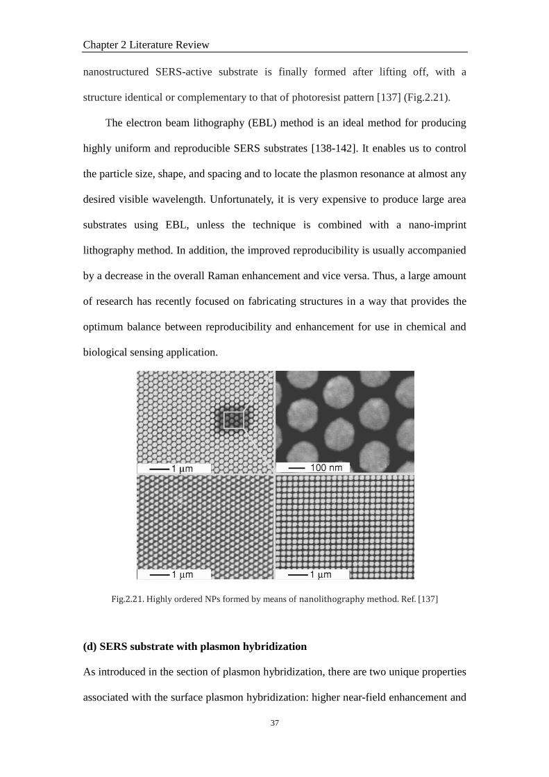
Chapter 2 Literature Review
37
nanostructured SERS-active substrate is finally formed after lifting off, with a
structure identical or complementary to that of photoresist pattern [137] (Fig.2.21).
The electron beam lithography (EBL) method is an ideal method for producing
highly uniform and reproducible SERS substrates [138-142]. It enables us to control
the particle size, shape, and spacing and to locate the plasmon resonance at almost any
desired visible wavelength. Unfortunately, it is very expensive to produce large area
substrates using EBL, unless the technique is combined with a nano-imprint
lithography method. In addition, the improved reproducibility is usually accompanied
by a decrease in the overall Raman enhancement and vice versa. Thus, a large amount
of research has recently focused on fabricating structures in a way that provides the
optimum balance between reproducibility and enhancement for use in chemical and
biological sensing application.
Fig.2.21. Highly ordered NPs formed by means of nanolithography method. Ref. [137]
(d) SERS substrate with plasmon hybridization
As introduced in the section of plasmon hybridization, there are two unique properties
associated with the surface plasmon hybridization: higher near-field enhancement and

Chapter 2 Literature Review
38
energy-splitting of plasmon-hybridized modes, respectively, both of which can be
employed for SERS.
Higher near-field enhancement
The superiority of a higher field enhancement is intuitive since the EM contribution to
the total SERS enhancement is proportional to the fourth power of the field
enhancement factor, as demonstrated in the section before. A well known substrate
that employs this property is the NP-dimer structure, with inter-particle separation at
the sub-nanometer scale (Fig.2.22). Raman enhancement on the order of 1014
has been
asserted [143-144], which is capable for single-molecule detection.
Fig.2.22. SERS substrates of metallic NP cluster with inter-particle junction. (a): dimer and (b): trimer.
A direct visualization of the high field enhancement induced by the LSP-LSP
hybridization was also experimentally demonstrated by F. Svedberg, etc. [16]. In their
experiment, a diffusing Ag-NP within the aqueous solution was trapped with an
optical tweezers and moved towards to another immobilized Ag-NP, both of which
were adsorbed with Raman molecules. As can be seen in Fig.2.23, in the case that the
two particles are separated far away, neither of them exhibits a SERS signal above the
noise level. A clear SERS spectrum only appears when the optically-trapped particle
is moved to the same position as the immobilized one and a SERS-active silver
particle dimer is thus created.
(a) (b)

Chapter 2 Literature Review
39
Fig.2.23. Inter-particle junction created by optical trapping technique and employed for SERS. (a)
SERS spectrum from a single immobilized particle (I) shows no signal. (b) An optically trapped
particle (T), without SERS signal, is moved toward the immobilized one. (c) When brought into
near-field contact, the particle pair (P) shows a strongly enhanced SERS signal. Ref. [16]
However, it is not easily to generate this kind of NP dimer or aggregate structures and
position the detected specimens exactly at the inter-particle junction. Moreover, the
SERS enhancement from NP aggregates will be strongly influenced by the size and
shape of the NPs, as well as the inter-particle spacing and incident light polarization.
Since the inter-particle spacing and arrangement for a NP aggregate is random, the
spectral intensity originated from NP aggregates is therefore quite irreproducible.
To overcome the low reproducibility of NPs aggregates, an alternative type of
junction is created by replacing one of the NPs with a smooth metal film, forming a
NP-film gap mode system [22-30]. Experimental studies demonstrated that such
NP-film junction is capable of providing remarkably reproducible SERS-active
compared with the NP-NP junction [27] (Fig.2.24). Moreover, due to the coupling
between the LSP excited on the NP and the SPPs generated on the conducting surface

Chapter 2 Literature Review
40
[37], the EM field enhancement shows more advantageous than that on a glass
substrate, in which only LSP mode is present. Hence, a NP-film junction shows a
good balance between the reproducibility and Raman enhancement.
Fig.2.24. NP-film junction as SERS substrate, which presents remarkable reproducibility as well as
high Raman enhancement. Ref. [27]
Energy-splitting of plasmon-hybridized modes
The energy-splitting of plasmon-hybridized modes can be employed for improving
the Raman enhancement as well [145-149]. The mechanism behind it is that since the
Raman peaks show a small wavelength-shift with respect to the incident illumination,
by carefully designing the structural parameters of the substrate such that the resonant
wavelengths of the bounding and anti-bounding plasmon-hybridized modes match the
excitation wavelength plus another specific Raman peak, the Raman intensity of that
peak can greatly be improved. For a clear demonstration, two of the examples are

Chapter 2 Literature Review
41
shown in Fig.2.25 (for LSP-LSP hybridization) and in Fig.2.26 (for LSP-SPP
hybridization), respectively.
Fig.2.25. Double-resonance SERS substrate with LSP-LSP interaction. (a) Schematic illustration of the
structure. (b) Simulated extinction (solid line) and near-field intensity (dashed line) spectra. Near-field
intensity spectrum shows intensity enhancement at a monitor point on the rod as a function of
illumination wavelength. Near-field spectrum exhibits two pronounced resonances at λ = 733 and 798
nm. (c) Normalized field distribution, |E|, for illumination at λ = 733 nm and (d) for illumination at λ=
798 nm. (e) Carefully designed substrate with resonant wavelengths match the excitation wavelength
and one of the Raman peak. (f) The improvement of Raman signal for the selected Raman peak. Ref.
[145]
(a) (b)
(c) (d)
(e) (f)

Chapter 2 Literature Review
42
Fig.2.26. Double-resonance SERS substrate with LSP-SPP interaction. (a) Schematic and SEM image
of the substrate. (b) Extinction cross-section and SERS spectrum of array with period of 780 nm.
Dashed line illustrates the excitation wavelength. Ref. [147]
2.3 Radial Polarization
Radially polarized light is gaining growing attention in the past decade due to its
advantages over the well known linearly and circularly polarized beams [150-162]. In
particular, it was shown that when using a high NA objective lens, the RP beam can
be focused to a much tighter spot compared with a linearly or circularly polarized
beam. This is mainly attributed to the strong longitudinal electric field component
generated at the focal plane [150, 153]. Owing to the unique properties of strong
longitudinal component and small spot size, the RP beam is well suited for a variety
of applications, including beam trapping [163], material processing [164], and optical
memories.
2.3.1 Beam Profile
The beam profile of a RP beam is quite different from that of conventional polarized
beams. Due to its singularity of polarization at the center, a RP beam has a donut
(a) (b)

Chapter 2 Literature Review
43
shape beam profile, with amplitude of electric field expressed as:
2
0 0
| | exp[ ( ) ]r
r rE
(2.25)
where r is the radial coordinate and ω0 represents the beam waist. Fig.2.27 presents
the beam shape of a RP beam and the comparison with a linearly polarized Gaussian
beam.
Fig.2.27. Beam shapes of a linearly polarized Gaussian beam (a) and a radially polarized beam (b),
respectively. (c) The corresponding amplitude distributions. The white arrows indicate the direction of
light polarizations.
2.3.2 Full p-polarized Beam
Because of its rotational symmetry of polarization, radially polarized light exhibits
focusing characteristics quite different from linearly polarized light. Fig.2.28 shows
the polarization characteristics of a linearly, radially, and azimuthally polarized light
when focused on to a planar interface. The first one on the left shows the optical ray
paths for a linearly polarized beam. In this case, the linearly polarized beam has an
0.0 0.5 1.0 1.5 2.0 2.5 3.0
0.0
0.2
0.4
0.6
0.8
1.0
r=0.707w0
Am
pli
tud
e
r/w0
Radial
Gaussian
r=w0
(a) (b)
(c)

Chapter 2 Literature Review
44
electric field that is horizontal and oriented parallel to the y-axis. Following the ray
paths through the lens we see that the electric field is perpendicular to the
plane-of-incidence (s-polarized or TE mode with respect to the surface) in the
y-axis/direction. Observing the electric field orientation in a similar manner along the
x-axis/direction, the optical paths now cause the electric field to be in the plane-of
incidence (p-polarized or TM mode). Thus there is no optical symmetry and the
surface at the focus is radiated by the varying degrees of either TM or TE type of
polarization depending on the path the ray took through the lens.
Fig.2.28. Comparison of the focusing properties of a linearly, radially and azimuthally polarized beam.
However, due to the rotational symmetry of both the radially and azimuthally type of
polarized beams, the beam is completely TM polarized (middle panel in Fig.2.28) in
all directions with respect to the surface for the radially polarized beam and
completely TE polarized (right panel in Fig.2.28) for the azimuthally polarized beam
irrespective of the ray path taken through the lens. This characteristic of having
complete TM polarization makes RP beams optimal for certain technological
applications and an ideal candidate for a variety of experiments in surface physics.

Chapter 2 Literature Review
45
2.3.3 SPPs Excitation Source
One of the most intriguing applications of radially polarized beams is to be employed
as the excitation source of SPPs. As mentioned previously, surface plasmon excitation
shows a strong dependence on the excitation polarization. In particular, under an ATR
excitation configuration, only p polarization can excite an SPP. This leads to an
interesting application of radially polarized beam in plasmonic focusing. More
specifically, when a radially polarized beam is launched into a dielectric/metal
plasmonic lens structures, the entire beam is p polarized with respect to the
dielectric/metal interface (Fig.2.29), providing an efficient way to generate a highly
focused surface plasmon through constructive interference and creating an strongly
enhanced local field, with the longitudinal component dominants the total electric
field (Fig.2.30). In contrast, if a highly focused linearly polarized beam is used to
excite the surface plasmons, because of the destructive interference between
counter-propagating surface plasmon waves, the focal field has a minimum at the
geometric focus.
Fig.2.29. (a) Diagram of SPP excitation with highly focused RP beam. (b) Back Fourier plane image of
the reflected beam, in which an axis-symmetric dark ring is observed that is due to the SPPs excitation.
Ref. [40]
(a) (b)
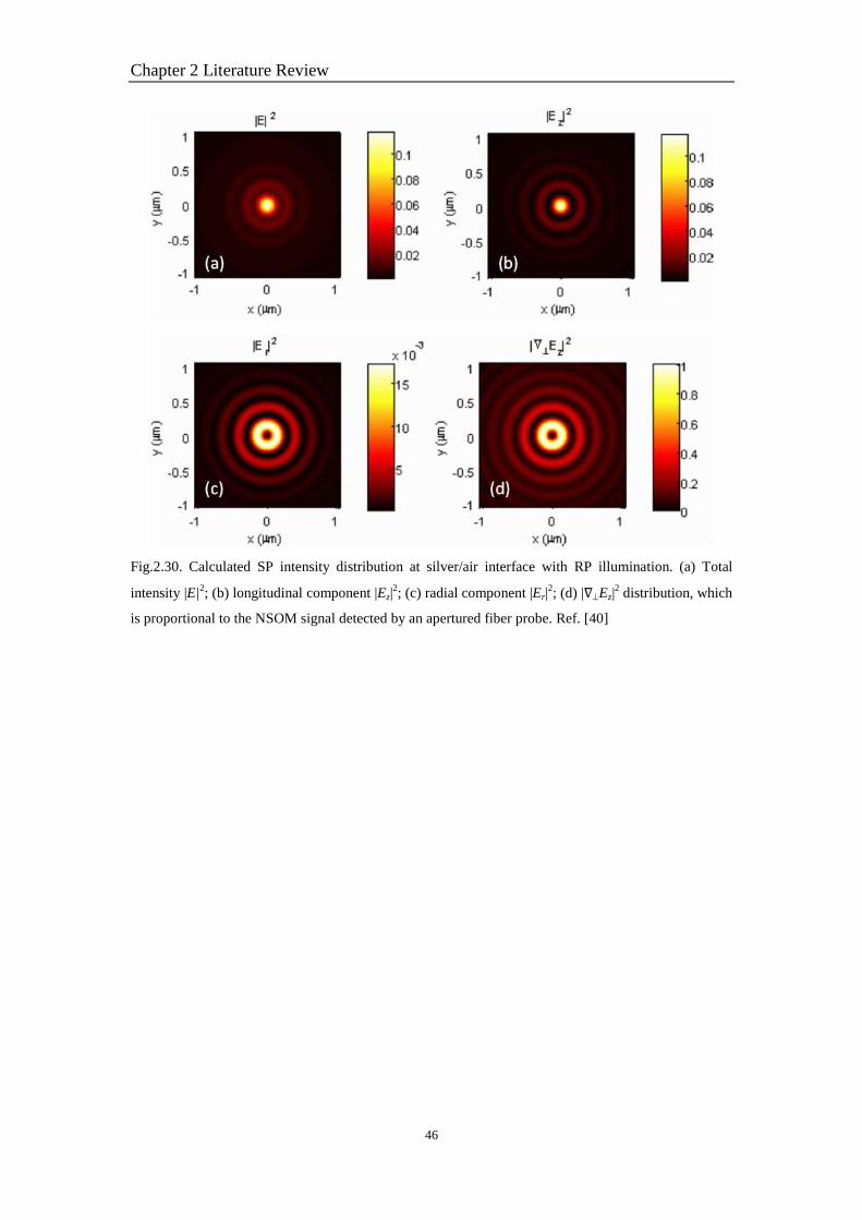
Chapter 2 Literature Review
46
Fig.2.30. Calculated SP intensity distribution at silver/air interface with RP illumination. (a) Total
intensity |E|2; (b) longitudinal component |Ez|
2; (c) radial component |Er|
2; (d) |∇Ez|
2 distribution, which
is proportional to the NSOM signal detected by an apertured fiber probe. Ref. [40]

Chapter 3 Surface Plasmon Coupling Mode – Numerical Investigation
47
Chapter 3 Surface Plasmon Coupling Mode
– Numerical Investigation
3.1 Chapter Introduction
Surface plasmon polaritons (SPPs) and localized surface plasmon (LSP) are two
different types of surface plasmon modes. For an SPP mode, two conditions should be
satisfied to excite an SPP: a p-polarized beam and the wave-vector matching
condition, respectively. As mentioned before, there are several approaches to realize
the wave-vector matching condition, such as ATR configuration, metallic grating
configuration, near-field scatter, etc. For an LSP mode, a p-polarized beam is
necessary as long as the excitation wavelength matches the resonant wavelength of
specific metallic nanostructure. In previous research work by other groups, LSP was
generally excited by free space propagating radiation, and LSP and SPPs were
investigated separately for their specific applications. In this chapter, as a fundamental
investigation, two types of excitation configurations are proposed and numerically
studied, in which SPPs and LSP are excited simultaneously, resulting in a surface
plasmon coupling mode (or called plasmon-hybrid-mode elsewhere).
The first one consists of a two-dimensional dielectric grating covered by a silver
film with thickness of tens of nanometers. SPP excitation conditions are fulfilled
through the metallic grating, while LSP is excited on the metallic bumps. Resonant
wavelengths of SPPs and LSP can effectively be tuned via changing the structural
period and the thickness of silver film. At specific wavelength, LSP and SPPs can
co-exist, leading to a surface plasmon coupling mode.
For the second configuration, a RP light is tightly-focused onto a silver-air
interface by a high NA objective lens. SPPs are thus excited under an ATR

Chapter 3 Surface Plasmon Coupling Mode – Numerical Investigation
48
configuration. The SPPs subsequently interact with a silver nanosphere on top of the
silver film to excite the LSP.
In both plasmon-hybrid-mode systems, the three-dimensional FDTD method is
employed to investigate their plasmonic response. In particular, electromagnetic
enhancement was studied under the surface plasmon coupling mode. The studies in
this chapter will provide important information for the following experiments as well
as the application based on the plasmon-hybrid-mode.

Chapter 3 Surface Plasmon Coupling Mode – Numerical Investigation
49
3.2 Surface Plasmon Coupling Mode Induced by
Periodic Metallic Structure
3.2.1 Structure
Fig.3.1 shows the proposed structure studied in this section. Briefly, a
two-dimensional array of SiO2 cuboids with fixed size of 50 50 100 nm3 is
patterned on the Si substrate, with a layer of 40-nm-thick silver film covered on the
surface. An array of cubic bumps is formed as viewed from the top. Obviously, such a
structure can easily be fabricated using the conventional silicon process technology.
Fig.3.1. Schematic of the proposed structure and its cross-sectional view along the dashed line.
To obtain the plasmonic response of such a structure, the DiffractMod package based
on rigorous coupled wave analysis in the commercial software R-Soft is applied. For
water (as the environment), Si, and SiO2, the refractive indices are set to be 1.3364,
3.99, and 1.5458, respectively. For silver, which is a lossy material possessing
wavelength-dependent dielectric constant, the refractive index is obtained from Ref.
[50] in the visible range (400 nm - 800 nm). We choose water as the environment in
this work because SERS are widely used in the area of bio-sensing and bio-imaging,
in which the sample is typically aqueous.

Chapter 3 Surface Plasmon Coupling Mode – Numerical Investigation
50
3.2.2 Simulation Results
Fig.3.2 shows the absorption characteristics based on various configurations. Using
the semi-infinite water-silver flat interface model (dashed line), the reflectance at the
interface for normal incidence is: R = ((n0 – nr)2 + k
2) / ((n0 + nr)
2 + k
2), where n0 is
the refractive index of environment, nr the real part of the refractive index of silver
and k the imaginary part which gives rise to the absorption in the silver. For a
40-nm-thick silver film sandwiched between semi-infinite water and Si (dotted line),
the absorption will decrease slightly and transmission appears due to the finite
thickness of the silver film. Further, if we produce the two-dimensional infinite
dielectric grating and cover the whole surface conformally by a 40-nm-thick silver
film, multiple absorption peaks will present in the absorption spectrum due to the
excitation of LSP and SPP (solid line). The broad ones denoted as peaks 2 and 3 in
Fig.3.2 correspond to the first-order LSP and high order LSP, respectively, whereas
the sharp one denoted as peak 1 corresponds to the SPP.
At normal incidence, the SPPs can be excited in a periodic structure satisfying
02 / ( ) / ( )m e m ek (3.1)
where Λ is the structural period, k0 the wave-number of light in vacuum, and εm and εe
the permittivity of metal and environment, respectively. The term on the right hand
side of Eq. (3.1) represents the wave-number of the SPP propagating along the single
interface. Equation (3.1) predicts an SPP excitation wavelength of 670 nm for Λ = 475
nm, which is slightly longer than the numerical simulation result (637 nm). The
difference is due to the modification of Eq. (3.1) for periodic bump structures. Fig.3.3
gives the near-field distributions at different resonant conditions in the solid-line
curve in Fig. 3.2, which is obtained by applying the FullWave Package based on the
FDTD method in R-Soft. In the simulation, the grid size is set to be 2 nm and the

Chapter 3 Surface Plasmon Coupling Mode – Numerical Investigation
51
periodic boundary conditions are set for X and Y directions and the perfectly matched
layer for Z direction.
0.4 0.5 0.6 0.7 0.80.0
0.1
0.2
0.3
0.4
0.5
0.6
0.7
Ab
sorp
tio
n
/m
1 2
3
Fig.3.2. Absorption spectra based on: semi-infinite water-silver flat interface configuration (dashed
line), 40-nm-thick silver film sandwiched between water and Si configuration (dotted line), and
dielectric grating covered by 40-nm-thick silver film configuration (solid line).
For the numerical investigation, two methods are generally employed to estimate the
Raman enhancement: the maximum enhancement factor (EF_max) and the averaged
enhancement factor (EF_ave), respectively.
For an arbitrary localized plasmon mode, for example, the dipolar plasmon mode
on a sphere-shaped NP as shown in Fig.2.9 (b), the electric field is typically
spatially-variant over the surface of particle. As a result, the enhancement factor for
molecules adsorbing at different sites are different. The maximum Raman
enhancement factor is therefore defined as: |Emax|4/|E0|
4, where Emax is the maximum
electric field over the particle surface from the excitation of plasmon mode while E0
the incident electric field. The logic behind such definition is based on the assumption
that the concentration of molecules and NPs within their specific solutions during
preparation is comparable such that there are, statistically, only few molecules
adsorbing at the NP. One typical example is the single molecule SERS (SM-SERS), in
which only single molecule is attached on the NP. Under this circumstance, the
maximum enhancement factor is meaningful since the SM-SERS is realized generally
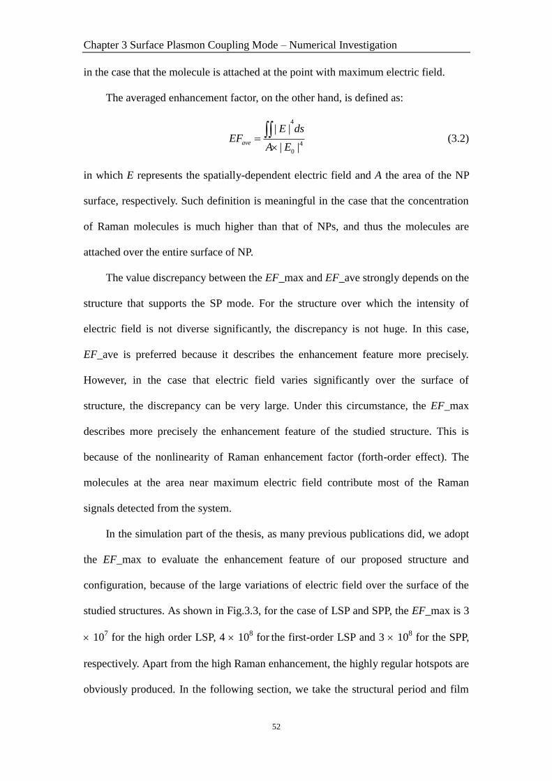
Chapter 3 Surface Plasmon Coupling Mode – Numerical Investigation
52
in the case that the molecule is attached at the point with maximum electric field.
The averaged enhancement factor, on the other hand, is defined as:
4
4
0
| |
| |ave
E dsEF
A E
(3.2)
in which E represents the spatially-dependent electric field and A the area of the NP
surface, respectively. Such definition is meaningful in the case that the concentration
of Raman molecules is much higher than that of NPs, and thus the molecules are
attached over the entire surface of NP.
The value discrepancy between the EF_max and EF_ave strongly depends on the
structure that supports the SP mode. For the structure over which the intensity of
electric field is not diverse significantly, the discrepancy is not huge. In this case,
EF_ave is preferred because it describes the enhancement feature more precisely.
However, in the case that electric field varies significantly over the surface of
structure, the discrepancy can be very large. Under this circumstance, the EF_max
describes more precisely the enhancement feature of the studied structure. This is
because of the nonlinearity of Raman enhancement factor (forth-order effect). The
molecules at the area near maximum electric field contribute most of the Raman
signals detected from the system.
In the simulation part of the thesis, as many previous publications did, we adopt
the EF_max to evaluate the enhancement feature of our proposed structure and
configuration, because of the large variations of electric field over the surface of the
studied structures. As shown in Fig.3.3, for the case of LSP and SPP, the EF_max is 3
107 for the high order LSP, 4 10
8 for
the first-order LSP and 3 10
8 for the SPP,
respectively. Apart from the high Raman enhancement, the highly regular hotspots are
obviously produced. In the following section, we take the structural period and film

Chapter 3 Surface Plasmon Coupling Mode – Numerical Investigation
53
thickness as variables and investigate their effects on the Raman enhancement.
Fig.3.3. |E|2 distributions at the top of cubic bumps along XY plane at various resonant conditions,
i.e., the incident wavelength of (a) 450 nm corresponding to the high order LSP, (b) 637 nm to the SPP,
and (c) 670 nm to the first-order LSP. The colorbar scale is set as log10(|E|2).
Fig.3.4 (a) shows a set of absorption spectra for the period ranging from 402 nm to
546 nm with a step of 24 nm. The peak absorption wavelengths are denoted as λmax
and their plots against the structural period for both the LSP and SPP are shown in
Fig.3.4 (b). The red-shift trend of the resonant wavelength for SPP for increasing
period can be predicted from the excitation condition [Eq. (3.1)]. As the structural
period increases, the right hand side value in Eq. (3.1) should be lower accordingly to
satisfy the condition. Because of the dispersion property of silver refractive index in
visible range, a red-shift of excitation wavelength is required from calculation. For the
LSP, the resonant wavelength is affected by the distance between bumps. For large
structural period, meaning bumps are separated far away; the plasmon resonant
wavelength shift is resulting from the long-range interactions. From Fig.3.4 (b), LSP
resonant wavelength shows slightly blue shift as bumps distance is decreased, which
is consistent with previous work [165-166].
The Raman enhancement shows a great dependence on the structural period
because of the interaction between the LSP and SPP. In Fig.3.4 (b), two peaks can be
found from the |Emax(λ)| plot for the resonant wavelength of SPP at each period (green
curve with triangles). The red (with circles) and black (with squares) curves clearly
0
1
2
3
1
10
102
103
0
1
2
3
1
10
102
103
0
1
2
3
1
10
102
103
(a) (b) (c)
0
1
3
2
0
1
3
2
0
1
3
2

Chapter 3 Surface Plasmon Coupling Mode – Numerical Investigation
54
show that there is an intersection between them, implying the occurrence of LSP and
SPP at the same wavelength. In this case, strong coupling between the SPP and LSP
will occur, leading to a considerable enhancement of the local electric field
responsible for the right peak in the |Emax(λ)| curve. As for the left peak at smaller
wavelength, the analysis of the |E(λ)| distribution shows that it is from the coupling
between the SPP and the second-order LSP.
Fig.3.4. (a) Absorption spectra for various periods from 426 nm to 546 nm with a 24 nm increment;
(b) absorption peak positions versus different periods for LSP (circles) and SPP (squares), with
corresponding maximum local |E| at resonant wavelength of SPP (triangles). The silver film thickness
is 40 nm, the bump height is 100 nm and the environment is water.
Next, we consider the influence of the silver film thickness to the resonant wavelength
and Raman enhancement. For a fixed structural period, the resonant wavelength of
SPP remains constant approximately. For the LSP, as film thickness is increased, three
aspects should be considered which can contribute to the wavelength shift. Firstly, the
distance between the bumps decreases for increasing film thickness. As stated above,
this causes slightly blue shifts of the resonant wavelength. Secondly, since the
nanoparticle (bump here) is not pure metal, as film thickness increases, the effective
refractive index of nanoparticle will change accordingly, which induces slightly blue
shifts as well. Thirdly, the size and shape of the nanoparticle play an important role in
determining the plasmon resonant wavelength. As film thickness increases, the size of
nanoparticle largens and the shape becomes more oblate, both effects contribute to a
400 420 440 460 480 500 520 540 560450
500
550
600
650
700
750
90
95
100
105
110
115
120
125
130
|E| m
ax
m
ax (
nm
)
Period (nm)
SPP
LSP
b
500 550 600 650 700 750 8000.0
0.1
0.2
0.3
0.4
0.5
0.6
0.7
nm)
Ab
sorp
tio
n
=426,450,474,
498,522,546 nm
a
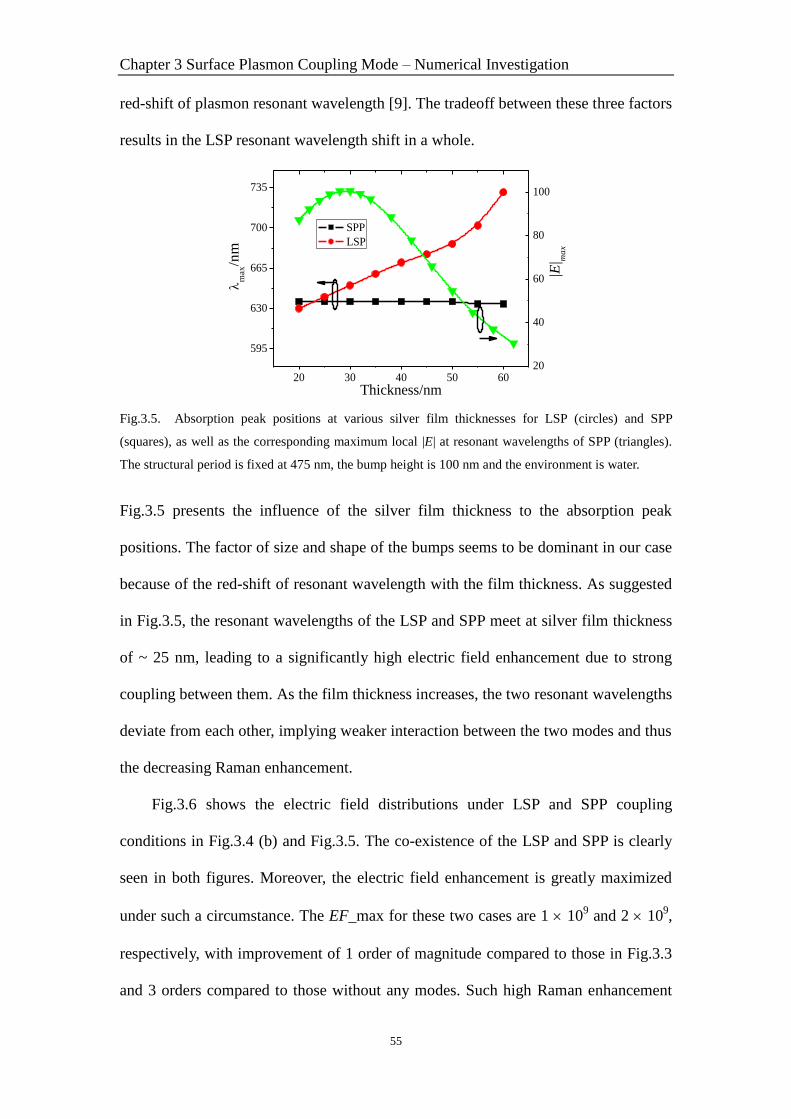
Chapter 3 Surface Plasmon Coupling Mode – Numerical Investigation
55
red-shift of plasmon resonant wavelength [9]. The tradeoff between these three factors
results in the LSP resonant wavelength shift in a whole.
20 30 40 50 60
595
630
665
700
735
20
40
60
80
100
|E| m
ax
m
ax/n
m
Thickness/nm
SPP
LSP
Fig.3.5. Absorption peak positions at various silver film thicknesses for LSP (circles) and SPP
(squares), as well as the corresponding maximum local |E| at resonant wavelengths of SPP (triangles).
The structural period is fixed at 475 nm, the bump height is 100 nm and the environment is water.
Fig.3.5 presents the influence of the silver film thickness to the absorption peak
positions. The factor of size and shape of the bumps seems to be dominant in our case
because of the red-shift of resonant wavelength with the film thickness. As suggested
in Fig.3.5, the resonant wavelengths of the LSP and SPP meet at silver film thickness
of ~ 25 nm, leading to a significantly high electric field enhancement due to strong
coupling between them. As the film thickness increases, the two resonant wavelengths
deviate from each other, implying weaker interaction between the two modes and thus
the decreasing Raman enhancement.
Fig.3.6 shows the electric field distributions under LSP and SPP coupling
conditions in Fig.3.4 (b) and Fig.3.5. The co-existence of the LSP and SPP is clearly
seen in both figures. Moreover, the electric field enhancement is greatly maximized
under such a circumstance. The EF_max for these two cases are 1 109 and 2 10
9,
respectively, with improvement of 1 order of magnitude compared to those in Fig.3.3
and 3 orders compared to those without any modes. Such high Raman enhancement

Chapter 3 Surface Plasmon Coupling Mode – Numerical Investigation
56
ensures this structure as a potential substrate and this plasmon-hybrid-mode system as
a potential mechanism for high sensitive molecule detection.
Fig.3.6. |E|2 distributions under surface plasmon coupling conditions in Fig.3.4 (b) (left), and in
Fig.3.5 (right), respectively. The colorbar scale is set as log10(|E|2).
3.2.3 Summary
We have investigated the plasmonic properties of a potential SERS substrate, on
which both the LSP and SPP can be excited. The FDTD simulation shows that the
resonant wavelengths of LSP and SPP can effectively be tuned via changing the
structural period and the silver film thickness. LSP and SPP can co-exist at specific
wavelengths such that the coupling between them can contribute to a considerable
boost of Raman enhancement. Raman enhancement of more than 109 is achieved in
the proposed structure, under the plasmon-hybrid-mode. This work illustrates a
structure with large area, regular hotspots, as well as extremely high Raman
enhancement. It is a good candidate for SERS substrates as it can be easily fabricated
using conventional silicon process technology.
0
1
2
3
4
10
0
1
2
3
4(a) (b)

Chapter 3 Surface Plasmon Coupling Mode – Numerical Investigation
57
3.3 Surface Plasmon Coupling Mode Induced by a
Tightly-Focused Radially-Polarized Beam
3.3.1 Excitation Configuration
Fig.3.7 presents the second optical configuration for a plasmon-hybrid-mode system.
A standard glass cover slip with refractive index of 1.5 is coated with a 45-nm-thick
silver film. A silver nanosphere with 60-nm-diameter is placed on the silver surface.
The gap between the objective lens and the cover slip is filled with an index matching
immersion oil. RP beam focused by a high NA objective lens is used as the excitation
light.
Fig.3.7. Proposed optical configuration through a high NA objective lens for plasmon-hybrid-mode,
in which a RP light is tightly focused onto a silver-air interface to excite SPPs, which subsequently
interact with a silver nanosphere on top of the silver film to excite LSP.
To excite the SPPs at the silver-air interface, on the one hand, the incident wavelength
and angle should satisfy the following wave-vector matching condition:
00 0
0
sin( ) msp sp
m
k k n k
(3.3)
where n is the refractive index of glass and matching oil, k0 the wave-vector of light in
Silver
Glass
Matching oil ,maxNA
SP
Optical Axis

Chapter 3 Surface Plasmon Coupling Mode – Numerical Investigation
58
vacuum, and εm and ε0 the permittivity of metal and air, respectively. The calculation
according to Eq. (3.3) indicates that resonant angle for the configuration ranges from
42 to 45 degrees over the 500 nm to 1000 nm spectrum region. This can readily be
realized as long as the maximum angle allowed by the objective lens exceeds the SP
resonance (SPR) angles. Meanwhile, the small variation of SPR angles ensures that
SPPs can be excited over the spectrum range we are interested. On the other hand, a
p-polarized beam is required to excite an SPP. For a RP beam, the entire beam is
p-polarized with respect to the silver-air interface. Thus, SPPs can be excited from all
azimuthal directions when a RP beam is tightly-focused onto a dielectric-metal
interface. The interference of the counter-propagating SPPs enables the formation of
an evanescent Bessel-like standing wave at the focal region. As can be seen later in
this work, such evanescent wave is well-suited as the excitation source of LSP on a
nanosphere-film junction.
3.3.2 Generation of Radial Polarization Numerically
Dissimilar with the conventional linear or circular polarization, radial polarization is
spatially-variant, and thus requires a tactical way to generate it, both in simulation and
experiment. In this thesis, a radial polarization derived from circular polarization is
employed numerically, which is based on the FullWave package within the
commercial software R-Soft.
Equation (3.4) and (3.5) shows the mathematical expression of a right-handed
and a left-handed circularly polarized beam, respectively. RP light is indirectly
achieved by the superposition of a right-handed circularly-polarized beam and a
left-handed circularly-polarized beam with a 2φ phase difference, where φ is the
azimuthal angle (Fig.3.8), as illustrated with Eq. (3.6).
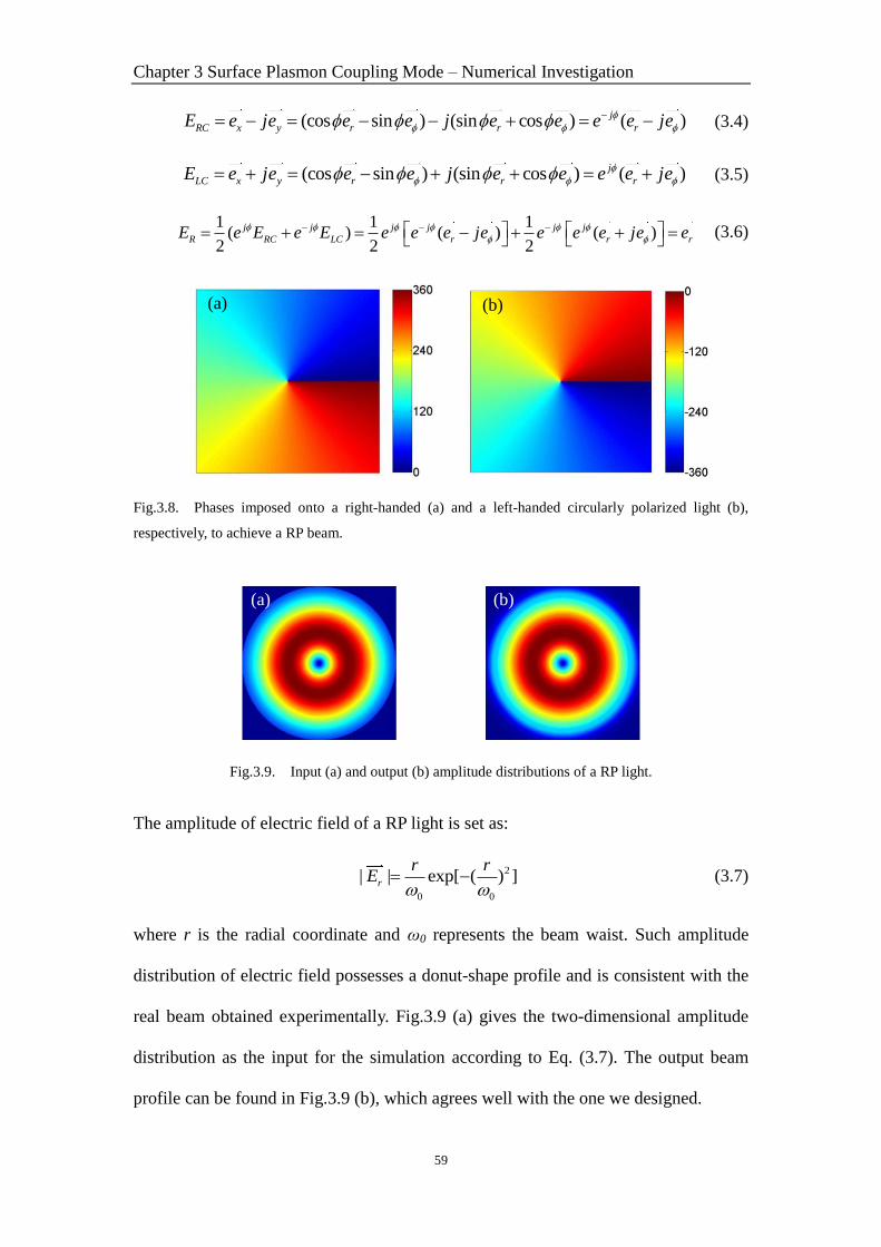
Chapter 3 Surface Plasmon Coupling Mode – Numerical Investigation
59
(cos sin ) (sin cos ) ( )j
RC x y r r rE e je e e j e e e e je
(3.4)
(cos sin ) (sin cos ) ( )j
LC x y r r rE e je e e j e e e e je
(3.5)
1 1 1( ) ( ) ( )
2 2 2
j j j j j j
R RC LC r r rE e E e E e e e je e e e je e
(3.6)
Fig.3.8. Phases imposed onto a right-handed (a) and a left-handed circularly polarized light (b),
respectively, to achieve a RP beam.
Fig.3.9. Input (a) and output (b) amplitude distributions of a RP light.
The amplitude of electric field of a RP light is set as:
2
0 0
| | exp[ ( ) ]r
r rE
(3.7)
where r is the radial coordinate and ω0 represents the beam waist. Such amplitude
distribution of electric field possesses a donut-shape profile and is consistent with the
real beam obtained experimentally. Fig.3.9 (a) gives the two-dimensional amplitude
distribution as the input for the simulation according to Eq. (3.7). The output beam
profile can be found in Fig.3.9 (b), which agrees well with the one we designed.
(a) (b)
(a) (b)

Chapter 3 Surface Plasmon Coupling Mode – Numerical Investigation
60
3.3.3 Realization of Tight Focus Numerically
The tight focus of a RP beam is realized by setting an initial equivalent phase function
of lens in the source file, instead of using the bulky objective lens to save the
computational memory and simulation time. The phase function is expressed as exp
(-ikr2/2f), where f represents the focal length. Combined with the amplitude and
phases imposed onto the circularly polarized lights, the final source file for a
tightly-focused RP beam is as following:
2 2_
0 0
1exp[ ( ) ]exp( / )( )
2
j jR focus RC LC
r rE ikr f e E e E
(3.8)
In the simulation, beam waist ω0 is set to be 6.5 μm and focal length f in the phase
function is set to be 7 μm. Such value combination of ω0 and f makes sure that the
amplitude peak of the generated RP light lies around the SPR angle, which optimizes
the excitation efficiency. Fig.3.10 shows a snapshot of the Ez component in the XZ
plane during the simulation. The tight focus of a RP beam can clearly be seen, with
the focal point marked by the circle with yellow color (number 1). The 45-nm-thick
silver film is located 2.5 μm below the focal plane. This treatment is to separate the
excited SPPs from the transmitted focused beam and hence reduce the influence from
the transmitted light. The excitation of SPPs can also clearly be seen just above the
silver film, which is indicated by the arrows with orange color (number 2). An
operation time of 20 (expressed in the unit of cT) is employed to make sure the
convergence of the simulation, as illustrated by the orange circle (number 3).

Chapter 3 Surface Plasmon Coupling Mode – Numerical Investigation
61
Fig.3.10. Illustration of a tightly-focused RP light realized by setting an initial equivalent phase
function of lens in the source file; 1: the focal point of the system, which is determined by the phase
function of lens; 2: indication of the excitation of SPPs from all directions; 3: convergence verification
of the simulation to ensure the accuracy.
3.3.4 Simulation Results
In the following numerical simulation, refractive indices of glass and matching oil are
set to be 1.5, and that of silver is obtained from Ref. [50]. The grid size within the
silver film and silver nanosphere is set to be 2 nm to ensure the simulation accuracy,
and the perfectly-matched layer boundary conditions are set for X, Y and Z directions.
Fig.3.11 presents the longitudinal field (Ez) distribution around the metal film
under a tightly-focused RP beam, in the absence of a nanosphere on the metal film.
The transversal component (Er) is not shown here because its intensity is much
smaller than that of the Ez component (~0.1|Ez|2) and hence plays a tiny role. An
interference pattern can clearly be seen in Fig.3.11, with a sharply-confined spot
1
2 2
3
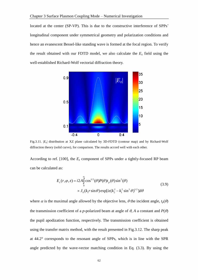
Chapter 3 Surface Plasmon Coupling Mode – Numerical Investigation
62
located at the center (SP-VP). This is due to the constructive interference of SPPs’
longitudinal component under symmetrical geometry and polarization conditions and
hence an evanescent Bessel-like standing wave is formed at the focal region. To verify
the result obtained with our FDTD model, we also calculate the Ez field using the
well-established Richard-Wolf vectorial diffraction theory.
Fig.3.11. |Ez| distribution at XZ plane calculated by 3D-FDTD (contour map) and by Richard-Wolf
diffraction theory (solid curve), for comparison. The results accord well with each other.
According to ref. [100], the Ez component of SPPs under a tightly-focused RP beam
can be calculated as:
1/2 2
0
2 2 2 1/2
0 1 2 1
( , , ) 2 cos ( ) ( ) ( )sin ( )
( sin )exp[ ( sin ) ]
z pE r z i A P t
J k r iz k k d
(3.9)
where is the maximal angle allowed by the objective lens, the incident angle, tp()
the transmission coefficient of a p-polarized beam at angle of , A a constant and P()
the pupil apodization function, respectively. The transmission coefficient is obtained
using the transfer matrix method, with the result presented in Fig.3.12. The sharp peak
at 44.2° corresponds to the resonant angle of SPPs, which is in line with the SPR
angle predicted by the wave-vector matching condition in Eq. (3.3). By using the
|Ez|

Chapter 3 Surface Plasmon Coupling Mode – Numerical Investigation
63
Richard-Wolf method, the Ez field distribution along x direction at z = 0 was obtained
and illustrated with the solid line in Fig.3.11. As can be seen, the positions of
interference fringes agree well with that obtained with the FDTD model and hence
verifying the validity of our 3D-FDTD model.
40 42 44 46 48 50
0
20
40
60 Glass/Ag/Air
Tra
nsm
issi
on
Incident angle
Fig.3.12. Transmission of a 45-nm-thick silver film sandwiched by semi-infinite air (n=1) and glass
(n=1.515), obtained with the transfer matrix method.
Next, a silver nanosphere with 60-nm-diameter is placed at the center of SPP standing
-wave just above the silver film, to investigate the nanosphere-SPP interaction.
Fig.3.13 (a) presents a contour map of electric energy density around the nanosphere
at a 532nm incident wavelength excitation. As can be seen, a vertically-oriented
dipolar-like mode is excited by the longitudinal component of SPP standing-wave,
with electric field at the nanosphere-film junction significantly concentrated and
enhanced. To make sure the accuracy and reliability of the calculation, we extract the
maximum electric field at the nanosphere-film gap by a first-order exponential-decay
-fitting of the data near the interface along the red dashed line as indicated with the
inset in Fig.3.13 (b), instead of simply using the maximum value obtained by the
simulation. The fitting curve along with the original data can be found in Fig.3.13 (b),
which shows an excellent agreement with each other. The derived fitting value A+y0,

Chapter 3 Surface Plasmon Coupling Mode – Numerical Investigation
64
which represents the maximum intensity of electric field at the gap (x=0), will be used
to characterize the enhanced electric field in the following work.
Fig.3.13. (a) Contour map of electric energy density around the nanosphere at a 532 nm incident
wavelength excitation. (b) Exponential-decay-fitting of the electric energy density in the vicinity of the
nanosphere-film junction along the dashed red line as illustrated with the inset.
Fig.3.14 presents the maximum electric field enhanced at the gap plotting against the
incident wavelength from 380 nm to 560 nm (blue curve). A controlled excitation
scheme, in which the 45-nm-thick silver film was replaced by a glass film with
identical thickness, was introduced in this study for the purpose of comparison. The
calculated result with the same method is shown in Fig.3.14 with the red curve. Under
the controlled scheme, the replacement of the metal film with a glass film avoids the
excitation of SPPs at the film surface. In other words, the LSP excitation for the
controlled one is totally due to the focused RP beam, rather than the SPPs standing
-wave, and hence no SPP & LSP coupling mode exists.
As can be seen in Fig.3.14, from the resonant wavelength point of view, the peak
of enhanced electric field occurs at 410 nm in the case of 45-nm-glass film, compared
to the 500 nm resonant wavelength in the presence of SPPs. The red-shift of resonant
wavelength is believed due to the strong interaction between the SPP standing-wave
on the silver film and the LSP excited on the nanosphere and is in line with the
preceding work [84]. From the perspective of field enhancement, the optimized
0 5 10 15 20 25 30
0
100000
200000
300000
400000
500000
600000
700000
800000
Original data
Exponential-decay-fitting
Fitting information:
Equation: y = A*exp(-x/t) + y0
R^2 = 0.99346
y0 7601.64615
A 1536080.33225
t 2.80776
Inte
nsi
tyDistance / nm
(b)
x / m
-0.4 0 0.4
-0.4
0
0.4
1
2
3
4
5
6(a)

Chapter 3 Surface Plasmon Coupling Mode – Numerical Investigation
65
enhanced electric field is 6.6 106 under resonant condition in the case of 45-nm
-thick silver film, while that from the controlled one is 1.35 105. The significant
enhancement effect for the proposed configuration attributes to two factors: from the
excitation of SPPs and from the LSP/SPPs coupling mode, respectively.
385 440 495 5500.0
0.3
0.6
0.9
1.2
0
2
4
6
105
Glass Film
En
han
ced |E
| 2En
han
ced
|E
|2
Wavelength / nm
Sivler Film
106
Fig.3.14. Enhanced electric fields at various incident wavelengths ranging from 380 nm to 560 nm for
the proposed (blue line) and controlled configurations (red line), respectively.
As introduced in the part of literature review, in a SERS system, the power of Raman
scattering radiation can be calculated by the following formula:
42
04
0
| |( ) | |
| |
locRS S SERS
EP N E
E (3.10)
where N is the number of Stokes–active scatters within the hotspot, SRES the
scattering cross-section, and Eloc and E0 the amplitudes of the enhanced and incident
electric field, respectively. In this work, SPPs are employed as the excitation source
and hence Eq. (3.10) becomes:
42
4
| |( ) | |
| |
locRS S SERS SPP
SPP
EP N E
E (3.11)
As indicated in Fig.3.11, the field enhancement induced by SPPs is on the order of 103

Chapter 3 Surface Plasmon Coupling Mode – Numerical Investigation
66
(|ESPP|2 ~ 35
2). Hence, that induced by LSP &SPPs coupling mode should be:
2 63
2 3
| | 6.6 106.6 10
| | 10
loc
SPP
E
E
(3.12)
and the total Raman enhancement is therefore on the order of 1010
. Similar calculation
for the controlled configuration results in a total Raman enhancement on the order of
107. Attention should also be paid on the field enhancement induced by LSP and SPPs
coupling mode, which is on the order of 6.6 103. This is greatly improved compared
to the one shown in Fig.2.9 (b), in which a standalone silver nanosphere with exactly
the same diameter is excited by a free-space propagating radiation and hence only
LSP mode is present. The maximum field enhancement is 100 in that case and 225 for
the controlled configuration in this study. It is 66 and 30 times improved, respectively,
after introducing the SPPs as the excitation source of LSP.
Fig.3.15. Electric field distributions under resonant wavelengths for the cases of 45-nm-thick silver
film (a) and 45-nm-thick glass film (b), respectively. The unit for x and y axis is m and the scale bar is
set as log10(|E|2).
Finally, the electric field distributions under resonant conditions are illustrated in
Fig.3.15, for the case of 45-nm-thick silver and glass film, respectively. In Fig.3.15 (a),
the presence of a metal film enables the excitation of SPPs. As a nanosphere placed
within the SPP region, LSP will be excited on the nanosphere and interacts with the
SPPs. The coupling between them results in a much higher field enhancement at the
-0.1 0 0.1
-0.1
0
0.1
2
3
4
5
6
-0.1 0 0.1
-0.1
0
0.1
3
4
5
Ag
Air
Glass
Air
Glass
(a) (b)
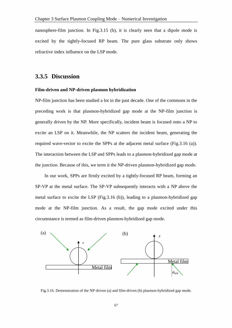
Chapter 3 Surface Plasmon Coupling Mode – Numerical Investigation
67
nanosphere-film junction. In Fig.3.15 (b), it is clearly seen that a dipole mode is
excited by the tightly-focused RP beam. The pure glass substrate only shows
refractive index influence on the LSP mode.
3.3.5 Discussion
Film-driven and NP-driven plasmon hybridization
NP-film junction has been studied a lot in the past decade. One of the commons in the
preceding work is that plasmon-hybridized gap mode at the NP-film junction is
generally driven by the NP. More specifically, incident beam is focused onto a NP to
excite an LSP on it. Meanwhile, the NP scatters the incident beam, generating the
required wave-vector to excite the SPPs at the adjacent metal surface (Fig.3.16 (a)).
The interaction between the LSP and SPPs leads to a plasmon-hybridized gap mode at
the junction. Because of this, we term it the NP-driven plasmon-hybridized gap mode.
In our work, SPPs are firstly excited by a tightly-focused RP beam, forming an
SP-VP at the metal surface. The SP-VP subsequently interacts with a NP above the
metal surface to excite the LSP (Fig.3.16 (b)), leading to a plasmon-hybridized gap
mode at the NP-film junction. As a result, the gap mode excited under this
circumstance is termed as film-driven plasmon-hybridized gap mode.
Fig.3.16. Demonstration of the NP-driven (a) and film-driven (b) plasmon-hybridized gap mode.
z
z
SPP
(a) (b)
Metal film
Metal film

Chapter 3 Surface Plasmon Coupling Mode – Numerical Investigation
68
The advantages of using our film-driven plasmon-hybridized gap mode for SERS are
two folds, as discussed in the section of “motivations”. First of all, the excitation
efficiency of SPPs is greatly improved by using the ATR configuration. In the case of
NP-driven gap mode, the SPPs formed on the metal surface are induced by the NP,
which diffracts the incident beam, generating the required wave-vector to match that
of SPPs. Such an excitation approach is rather inefficient and hence limiting its
Raman enhancement. Secondly, due to the vertical arrangement of an NP-film
junction, a longitudinal field component is preferred to efficiently excite a gap mode
at the junction. For an SP-VP excited by a tightly-focused RP beam, the portion of
longitudinal field is 98% at 532 nm, 99% at 633 nm and more than 90% over the
visible range. While in the case of NP-driven gap mode, a linearly polarized Gaussian
beam is focused directly on to the NP-film junction. A longitudinal field component
does exist under this kind of excitation approach. However, it is the subordinate field
component and the power utility is therefore quite low (Fig.3.17). Although RP beam
was also proposed as the excitation source for the NP-driven gap mode[84, 162], the
portion of longitudinal component (<80%) is still smaller than that of an SP-VP.
Fig.3.17. Transversal (left) and longitudinal (right) electric field distributions at the focal plane under a
tightly-focused linearly polarized Gaussian beam. NA=0.98. The smaller the NA, the stronger (weaker)
the transversal (longitudinal) field component.
-0.5 0 0.5
-0.5
0
0.5
0.02
0.04
0.06
0.08
0.1
0.12
0.14
-0.5 0 0.5
-0.5
0
0.5
0
0.005
0.01
0.015
0.02
0.025
0.03
|Er|2 |Ez|
2
x/μm x/μm
y

Chapter 3 Surface Plasmon Coupling Mode – Numerical Investigation
69
3.3.6 Summary
We proposed and numerically investigated a potential plasmon-hybrid-mode system,
in which a RP light is tightly-focused onto a silver-air interface to excite the SPPs.
The SPPs subsequently interact with a silver nanosphere on top of the silver film to
excite the LSP. In the simulation, RP beam is achieved by the superposition of a
right-handed and a left-handed circularly polarized beam with 2φ phase difference.
The FDTD simulation illustrates that the interaction between LSP and SPPs could
result in a remarkable red-shift of resonant wavelength with respect to the nanosphere
on a dielectric substrate, and a strong confinement of electric field at the
nanosphere-film junction. Electromagnetic field enhancement induced by the
film-driven plasmon-hybridized gap mode is on the order of 103, presenting more than
30-fold improvement compared to that from standalone LSP mode. Raman
enhancement of more than 1010
is achieved. It is 1000 times improved compared with
the controlled configuration, which is frequently used in a conventional optical
system.

Chapter 4 Surface Plasmon Coupling Mode for SERS
70
Chapter 4 Surface Plasmon Coupling Mode
for SERS
4.1 Chapter Introduction
In the previous chapter, we have numerically investigated two different types of
plasmon-hybrid-mode configurations, in which SPPs are excited by a metallic grating
structure and an ATR configuration, respectively. The electromagnetic enhancement
was significantly improved under the surface plasmon coupling mode compared to
that from the separate surface plasmon modes.
In this chapter, we will continue the work and investigate the performance of
plasmon-hybrid-mode system experimentally. More specifically, the hybrid mode
system induced by a tightly-focused RP beam will be introduced for surface-enhanced
Raman spectroscopy. The reasons why we choose the second configuration for the
experiment are three folds. Firstly, LSP is excited by an evanescent surface plasmon
standing-wave, which is a novel idea. In the previous research work, LSP was
generally excited by free space propagating radiations. Secondly, the preparation of
structure is relatively easy. No complicated fabrication process is required and the
only work is to immobilize silver nanospheres onto the silver film. Finally, using this
configuration for SERS possesses many advantages, including easily formed, high
predicted Raman enhancement and high reproducibility. These characteristics make it
a potentially-robust SERS substrate.
The organization of this chapter is as following: firstly, the generation of a RP
beam experimentally will be introduced; next, a sub-monolayer of silver nanospheres
will be immobilized onto a 45-nm-thick silver film, and interact with SPPs excited by
a tightly-focused RP beam. This experiment will present a qualitative view of the role
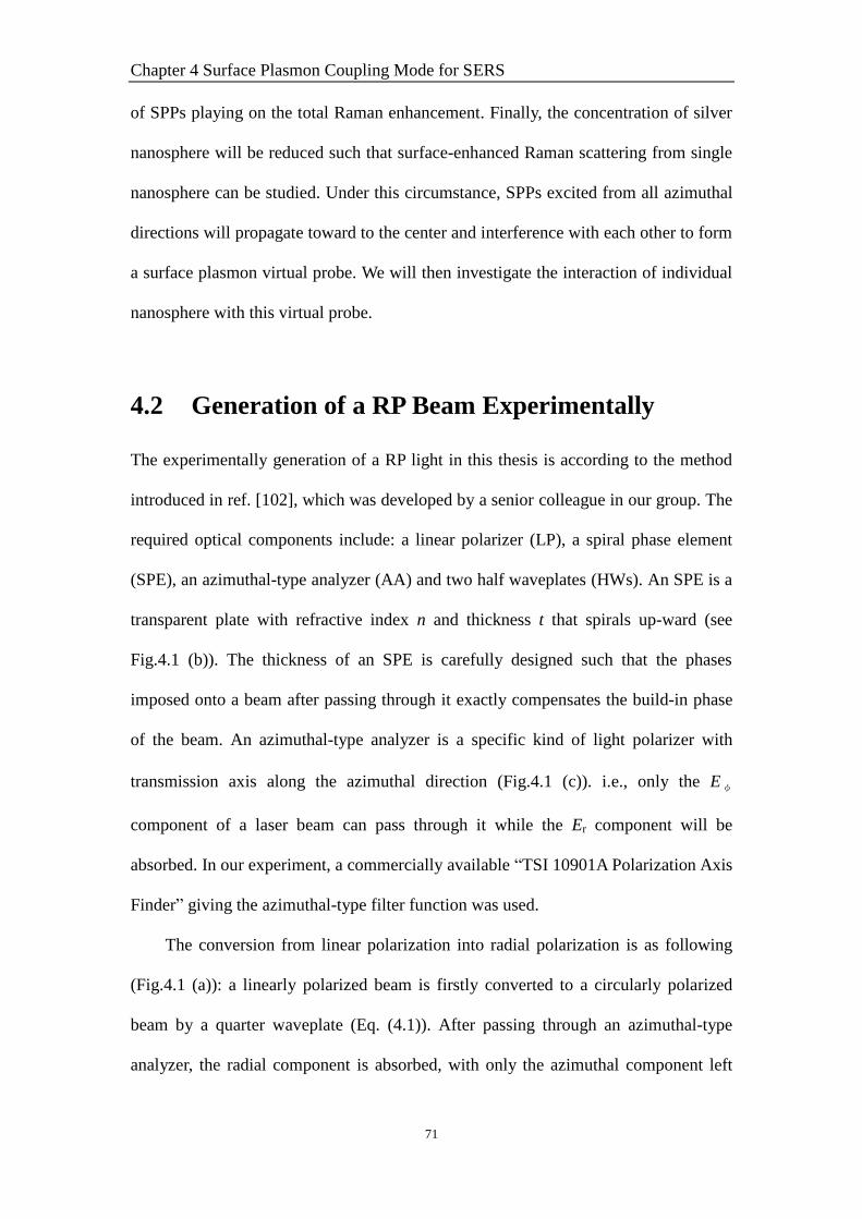
Chapter 4 Surface Plasmon Coupling Mode for SERS
71
of SPPs playing on the total Raman enhancement. Finally, the concentration of silver
nanosphere will be reduced such that surface-enhanced Raman scattering from single
nanosphere can be studied. Under this circumstance, SPPs excited from all azimuthal
directions will propagate toward to the center and interference with each other to form
a surface plasmon virtual probe. We will then investigate the interaction of individual
nanosphere with this virtual probe.
4.2 Generation of a RP Beam Experimentally
The experimentally generation of a RP light in this thesis is according to the method
introduced in ref. [102], which was developed by a senior colleague in our group. The
required optical components include: a linear polarizer (LP), a spiral phase element
(SPE), an azimuthal-type analyzer (AA) and two half waveplates (HWs). An SPE is a
transparent plate with refractive index n and thickness t that spirals up-ward (see
Fig.4.1 (b)). The thickness of an SPE is carefully designed such that the phases
imposed onto a beam after passing through it exactly compensates the build-in phase
of the beam. An azimuthal-type analyzer is a specific kind of light polarizer with
transmission axis along the azimuthal direction (Fig.4.1 (c)). i.e., only the Eφ
component of a laser beam can pass through it while the Er component will be
absorbed. In our experiment, a commercially available “TSI 10901A Polarization Axis
Finder” giving the azimuthal-type filter function was used.
The conversion from linear polarization into radial polarization is as following
(Fig.4.1 (a)): a linearly polarized beam is firstly converted to a circularly polarized
beam by a quarter waveplate (Eq. (4.1)). After passing through an azimuthal-type
analyzer, the radial component is absorbed, with only the azimuthal component left

Chapter 4 Surface Plasmon Coupling Mode for SERS
72
(Eq. (4.2)). A spiral phase element is then inserted to compensate for the geometric
phase, resulting in a non-charge azimuthally polarized beam (Eq. (4.3)). Two half
waveplates angled with 45 degrees between their optical axes are used finally to
convert the azimuthal polarization into radial polarization.
Fig.4.1. Generation and verification of a RP beam experimentally. (a) Illustration of an optical
configuration transferring a linearly polarized Gaussian beam into a RP beam. LP: linear polarizer, QW:
quarter waveplate, AA: azimuthal-type analyzer, SPE: spiral phase element, HW; half waveplate. (b)
Schematic view of an SPE and a real one. (c) Transmission axis of an azimuthal-type analyzer. (d)
Verification of a RP beam by using a linear polarizer.
( )j
LC x y rE e je e e je
(4.1)
j je e (4.2)
j j je e e je
(4.3)
The experimentally-achieved RP light is shown in Fig.4.1 (d), which possesses a
donut shape beam profile. This is due to the polarization singularity at the center of a

Chapter 4 Surface Plasmon Coupling Mode for SERS
73
RP beam. A linear polarizer is employed to verify its polarization distribution. As a RP
beam passes through a linear polarizer, the polarization along the transmission axis of
the linear polarizer will transmit while that orthogonal to the axis will be absorbed, in
between of these two directions, the polarized radiation is attenuated according to the
law of Malus. Hence the observed profiles have two distinct lobes along a line parallel
to the transmission axis of linear polarizer, as shown in Fig. 4.1 (c). In the following
experiments, the generated RP beam will be used as the excitation source.

Chapter 4 Surface Plasmon Coupling Mode for SERS
74
4.3 Nanosphere Sub-monolayer
4.3.1 Experimental Setup and Procedures
The schematic view of experimental setup is shown in Fig.4.2. RP beam as the
excitation light is achieved using the method just mentioned before. An Olympus oil
immersion objective lens (60 x, NA=1.49) is used to focus the collimated RP beam on
to the sample, composing a 45-nm-thick silver film deposited onto a cleaned cover
glass by electron beam evaporation, with 60-nm-diameter silver nanospheres
assembled on it. Raman signals originating from rhodamine 6G (R6G) molecules
sandwiched between the silver nanospheres and silver film are collected by an Ocean
Optics TEC cooling Raman spectrometer (TE 65000). A CCD camera is used at the
transmission direction to capture the Raman images of nanospheres, or at the back
Fourier plane to get the reflected laser beam.
Fig.4.2. Optical schematic of a plasmon-hybrid-mode based surface-enhanced Raman spectroscopy.
A 532nm RP beam is used as the illumination.
Silver nanospheres with diameter ~ 60 nm were purchased from nanoComposix. The
self assembly of silver nanospheres on the thin film surface was carried out by the

Chapter 4 Surface Plasmon Coupling Mode for SERS
75
following procedures: silver film with thickness of 45nm was first formed by electron
beam deposition on a cleaned glass coverslip. The coated substrate was then
immersed for around 30mins in a 10-7
M R6G solution to form a self-assembled
monolayer (SAM) of R6G molecules. The sample was subsequently rinsed with DI
water to remove excess molecules on the surface. Finally, a droplet of Ag colloids
(100 μl, ~1011
nanospheres / ml,) was applied onto the SAM/Ag plane and allowed to
evaporate naturally, followed by water-rinsing and air-drying at ambient temperature.
Dark-field image of the assembly of silver nanospheres on the silver film surface is
shown in Fig.4.3. A sub-monolayer of silver nanospheres can clearly be seen, with
most of the particles be isolated and uniformly distributed on the surface.
Fig.4.3. Dark-field image of immobilized silver nanospheres on a 45-nm-thick silver film.
4.3.2 Experimental Results and Discussion
Based on the Kretschmann configuration, SPPs can be excited to satisfy:
0 0 0 0sin / ( )oil sp spp m mk n k k (4.4)
where k0 is the wave-vector of light in vacuum, θsp the SPR angle, and εm and ε0 the
permittivity of metal and environment (air in our work), respectively. The predicted

Chapter 4 Surface Plasmon Coupling Mode for SERS
76
resonant angle for 532 nm illumination according to Eq. (4.4) (θsp =44.2°) is smaller
than the maximum angle allowed by the oil immersion objective lens with 1.49 NA
(αmax = 79), which assures the excitation of SPPs in our work. Fig.4.4 presents the
Raman images of nanospheres immobilized on the silver film captured by the CCD
camera at various sample-objective lens distances (a-i), as well as the illustrations of
three types of excitation schemes (j-l).
When the sample-objective lens distance is beyond the focal length (post-focal
plane scheme), as shown in Fig.4.4 (j), RP beam will be focused on to the silver-air
interface divergently, and so are the transversal components of wave-vector at silver
film surface, which determine the propagating direction of SPPs. Since the entire
beam for a RP beam is p-polarized, SPPs will be excited from all directions, forming
an excitation circle, and propagate from the excitation circle divergently under the
post-focal plane circumstance, as shown in Fig.4.4 (a), with the dashed yellow circle
representing the excitation circle of SPPs. It can clearly be seen that silver
nanospheres within the propagation region of SPPs are effectively activated, while
those out of the SPP region cannot be detected due to their relatively low Raman
enhancement. This demonstrates that the interaction of SPPs with nanospheres on top
of the silver film can effectively excite the LSP on each nanosphere, leading to an
impressive Raman enhancement. Attention should also be paid on the activated band
with limited length, in which the intensity of Raman signals from activated
nanospheres is gradually attenuated along positive radial direction. This is mainly due
to the limited propagation length of SPPs and the exponentially-decaying of electric
field as it propagates along radial direction.
Chapter 4 Surface Plasmon Coupling Mode for SERS
77
Fig.4.4. Raman images of silver nanospheres immobilized on a silver film surface at various
sample-objective lens distances obtained by a CCD camera (a-i), and the corresponding types of
excitation schemes. (j): post-focal plane, (k): on-focal plane and (l): pro-focal plane schemes.
As the sample-objective lens distance decreases, the SPPs excitation circle becomes
smaller since its size is proportional to the sample-focal plane displacement. However,
as long as their distance goes beyond the focal length, SPPs will propagate from the
excitation circle divergently, as demonstrated in Fig.4.4 from (a) to (d).Turning point
occurs when the sample locates exactly at the focal plane of objective lens (on-focal
plane scheme), as shown in Fig.4.4 (k). Under this circumstance, RP beam will be
focused onto the silver-air interface into a minimum spot, within which SPPs are
excited and propagate around. Likewise, silver nanospheres within the propagation
region of SPPs will be activated and detected by the CCD camera (Fig.4.4 (e)).
Further decrease of sample-objective lens distance results in the incident beam be
focused onto the silver-air interface convergently (pro-focal plane scheme). Hence,
SPPs excited under this circumstance will propagate convergently into the center from
a b c
d e f
g h i
j
k
l Ksp
Ksp

Chapter 4 Surface Plasmon Coupling Mode for SERS
78
the excitation circle, whose size becomes larger as sample-objective lens distance
further decreases, as illustrated in Fig.4.4 (f-i). To sum up, SPPs excited by the RP
beam plays a significant role on the Raman enhancement of the system. Meanwhile,
our experimental result shown in Fig.4.4 indicates that a self assembly monolayer of
metal NPs (adsorbed by detecting molecules) on a smooth metal film surface can
serve as a far field characterization of the excitation and propagation of SPPs, instead
of the near-field techniques such as NSOM.
Fig.4.5. Raman images of silver nanospheres obtained by a CCD camera when the sample locates
exactly at the focal plane of the objective lens, with (a) and without (b) the SPPs excitation. (c)
Demonstration of on-focal plane excitation scheme, under which incident beam is focused onto the
interface into a minimum spot. (d) Reflected laser beam obtained at the back Fourier plane. The sharp
dark ring represents a reflectivity dip thus indicating the SPPs excitation at the silver-air interface.
To further investigate the SPPs’ contribution on Raman enhancement and conduct a
direct comparison with the conventional NP-induced SPP&LSP coupling system, we
focus our study on the on-focal plane excitation configuration, as illustrated in Fig.4.5
(c). Also shown in Fig.4.5 (d) is the reflected laser beam obtained by the CCD camera
at the back Fourier plane. A sharp dark ring can clearly be seen at the reflected beam,
representing that incident beam at this angle is efficiently coupled to the SPPs. Thus,
as we control the RP beam size by an adjustable iris aperture just beneath the
a b
c d

Chapter 4 Surface Plasmon Coupling Mode for SERS
79
objective lens, and monitor the reflected beam at back Fourier plane, we can
conveniently switch “on” and “off” the excitation of SPPs.
Fig.4.5 (a) presents the Raman image of silver nanospheres with SPPs excitation
under the on-focal plane configuration. It is captured when the dark ring just comes
out at the reflected beam as we increase the incident beam size. While in Fig.4.5 (b),
which gives the Raman image of silver nanospheres without the SPPs excitation, is
captured when the dark ring just disappears as we decrease the beam size. The
comparison between Fig.4.5 (a) and (b) clearly indicates that the existence of SPPs
does lead to a significant improvement of Raman enhancement. Moreover, attention
should be paid on the circumstance when the dark ring just disappears and hence no
SPP is excited on the silver-air interface base on the TIRF configuration. In this case,
incident beam is focused and interacts with the nanospheres on the film to excite the
LSP, which is exactly the conventional NP-induced SPP&LSP co-enhanced system. In
other words, our experiment demonstrates that the introduction of propagating surface
plasmon into the conventional NP-film junction system brings on a significant
improvement on Raman enhancement
Subsequently, Raman spectra of R6G molecules adsorbed on silver nanospheres
at various RP beam sizes are obtained, as shown in Fig.4.6. The sample with much
less nanosphere density is prepared by reducing the silver colloid concentration and
immersion time. As can be seen from Fig.4.6, when RP beam size is too small to
cover the SPR angle, SPPs cannot be excited and hence no Raman signals can be
detected due to its limited Raman enhancement, as indicated by the black curve (a),
which is obtained when the beam size is controlled such that the dark ring at the back
Fourier plane just disappears. As incident beam size increases (red (b) and green (c)
curves), the dark ring comes out, meaning that SPPs are excited and interact with the

Chapter 4 Surface Plasmon Coupling Mode for SERS
80
nanospheres on the film surface. Raman enhancements under these circumstances are
significantly improved and remarkable SERS signal can be detected. Further increase
of beam size will not contribute to the Raman enhancement since the marginal beam
cannot couple to the SPPS due to their larger incident angle than the SPR angle.
Optimized condition occurs when the dark ring just totally comes out, with Raman
spectrum shown with the green curve (c). A 10 folds magnification of the black curve
indicates that Raman intensity for the smaller beam size is still 2 times weaker than
that of the green curve, which means the introduction of propagating surface plasmon
excitation based on a TIRF configuration induces an improvement of 20 times of the
Raman enhancement.
0 500 1000 1500 2000 2500 3000
0
20
40
60
80
100
e
f
d
b
c
Co
un
ts
Raman shifts / cm-1
a
Raman spectra
of R6G
Fig.4.6. Raman spectra of R6G molecules at various RP beam sizes, with a-f representing the
increase of beam size. Laser power incident onto the sample is approximately 500 μW. Integration time
of 1 second was used to collect the Raman signals.

Chapter 4 Surface Plasmon Coupling Mode for SERS
81
4.3.3 Summary
In summary, we qualitatively-demonstrated that Raman enhancement of conventional
NP-film junctions can significantly be improved by introducing the propagating
surface plasmon excitation based on the TIRF configuration. Experimental results
illustrate that silver nanospheres within the propagation region of SPPs are effectively
activated and detected from Raman images by a CCD camera due to their impressive
Raman enhancement. This intriguing phenomenon indicates that a self assembly
monolayer of metal NPs adsorbed with detecting molecules on a smooth metal film
can serve as a far field characterization of the excitation and propagation of SPPs,
instead of the near-field techniques such as NSOM. Raman enhancement presents
20-folds improvement compared with the NP-induced SPP/LSP co-enhanced Raman
spectroscopy. The impressive Raman enhancement along with its high reproducibility
of NP-film junction makes this configuration an attractive candidature for the
SPP-assisted gap-mode Raman spectroscopy.

Chapter 4 Surface Plasmon Coupling Mode for SERS
82
4.4 Single Nanosphere
In the previous experiment, a sub-monolayer of silver nanospheres was immobilized
on a silver film as the substrate for surface-enhanced Raman spectroscopy. Under this
circumstance, SPPs excited by a tightly-focused RP beam interact with nanospheres
very frequently and hence the interference of them is not notable.
In the following experiment, the density of nanospheres on the silver film is
significantly reduced so that only single nanosphere is within the propagation region
of SPPs. (Dark field image is shown in Fig.4.7). In this case, SPPs will propagate
freely along the metal surface and interfere with each other, forming an evanescent
standing-wave. An individual nanosphere will be moved into the SPPs region and the
SERS from single nanosphere-film junction will be investigated. 4-mba molecule will
be used in this section, due to its high power tolerance and pure Raman signals
without fluorescence, instead of the R6G molecules we used before.
Fig.4.7. Dark-field image of silver nanospheres with much lower density immobilized on a silver
surface. The yellow scale bar represents 5 m.
4.4.1 Surface Plasmon Virtual Probe
Numerically, electric field in the vicinity of the focus can be calculated with the
Richards-Wolf vectorial diffraction theory, with the results shown in Fig.4.8. Fig.4.8

Chapter 4 Surface Plasmon Coupling Mode for SERS
83
(a) exhibits the longitudinal field distribution under an RP beam illumination. The
transversal component is not shown here because of its much smaller intensity
compared to the longitudinal field, hence playing a tiny role in our work. As predicted,
because of the axially symmetric polarization of a PR light, SPPs excited from all
azimuthal directions interfere and form a Bessel-like standing-wave pattern, which
has a maximum intensity confined to a small region on the metal surface. It is
therefore termed as a surface plasmon virtual probe (SP-VP).
Fig.4.8. Longitudinal electric field distribution in the vicinity of the focus for a radially-polarized (a)
and a linearly-polarized Gaussian beam (b), respectively. (c) Electric field distribution around the silver
nanosphere as it locates at the center of SP-VP.
Also shown in Fig.4.8 (b) is the longitudinal field distribution produced from a
linearly polarized Gaussian beam with identical power, for the purpose of comparison.
As can be seen, the maximum intensity shows approximately 4-folds improvement in
the case of RP beam. The advantages of using a RP beam over a linearly polarized
beam are obvious: on the one hand, the excitation of SPPs performs an angular filter
function for the transmitted field. In other words, only the incident angles satisfying
the wave-vector matching condition can excite the SPPs. For a RP beam, the donut
shape beam profile shifts the power from center to higher inclination angle near the
dB
20
30
40
50
60c
100 nm
-0.50
0.5
-0.5
0
0.50
10
20
30
a
-0.50
0.5
-0.5
0
0.50
2
4
6
8
b

Chapter 4 Surface Plasmon Coupling Mode for SERS
84
SPR angle under a tight-focus configuration. This greatly improves the excitation
efficiency of SPPs compared to a Gaussian beam, for which most of the laser power
concentrated at the center. On the other hand, the Bessel-like standing-wave formed
under a RP beam has only one peak at the center (Fig.4.8 (a)), while there are two
longitudinal field lobes around the center in the case of a linearly polarized beam
(Fig.4.8 (b)), which halves the efficiency since only one of the two lobes will be used.
Fig.4.8 (c) presents the electric field distribution at the same region after a silver
nanosphere with 60-nm-diameter is placed at the center of the SP-VP, which is
calculated using the three-dimensional FDTD method with 2nm grid size. The result
clearly indicates that: firstly, the Bessel-like standing-wave pattern keeps well as that
in Fig.4.8 (a) in the presence of a nanosphere, meaning that the nanosphere shows
little influence on the excitation and propagation of SPPs, and hence the formation of
SP-VP. This is crucial as we intent to harness the virtual probe for single-NP-SERS.
Secondly, electric field is significantly concentrated at the nanosphere-film junction.
The maximum electric field is more than 106, which is much superior compared to
that from a standalone nanosphere without the metal film. The high electromagnetic
enhancement attributes to two factors: the formation of an SP-VP, which provides
102-10
3 enhancements, and the excitation of LSP/SPP coupling mode on the
nanosphere-film junction, which is responsible for approximately 104 enhancements,
as discussed in chapter 3.

Chapter 4 Surface Plasmon Coupling Mode for SERS
85
4.4.2 Experimental Results
Fig.4.9. SERS spectra of 4-mba molecules from single nanosphere-film junction located at the center
of SP-VP (Black) and without the excitation of SPPs (Red), respectively. The inset presents the
simultaneously captured Raman image of an individual silver nanosphere, with SPPs excitation.
Experimentally, because of the small region of SP-VP, a piezo-scanning-stage
(Physikinstrumente, P545, Nano XYZ stage) with 1-nm-resolution is used to search
and position the individual nanosphere. A CCD camera placed at the image plane in
the transmission direction is used to capture the Raman image of the nanosphere,
monitoring the intensity as we move the scanning stage. An adjustable iris aperture
placed just beneath the objective lens is used to manipulate the incident beam size.
The black curve in Fig.4.9 shows the SERS spectrum of 4-mba molecules collected
from a single nanosphere-film junction, with the inset showing the Raman image
captured by the CCD camera at the position of maximum Raman intensity. Under the
full beam illumination, nanosphere can clearly be seen, along with the Raman
spectrum with good signal to noise ratio obtained by the spectrometer (black curve).
As the beam size reduced such that the dark ring at the back Fourier plane just
disappears (Fig.4.5 (d)), meaning that no SPP is excited in this case, nanosphere
cannot be detected with the same exposure time as well as the Raman signals from the
0 500 1000 1500 2000 2500
0
20
40
60
1079.541375.82
1588.85
With SPPs
Ram
an
co
un
ts
Raman shifts / cm-1
W/O SPPs

Chapter 4 Surface Plasmon Coupling Mode for SERS
86
spectrometer (red curve). This clearly illustrates that it is the SPPs, rather than the
transmitted light, that contribute to the excitation of Raman signals.
-0.6 -0.4 -0.2 0.0 0.2 0.4 0.6
0.0
0.2
0.4
0.6
0.8
1.0
Simulation
ExperimentN
om
aliz
ed I
nte
rnsi
ty
X Axis / m
Fig.4.10. Normalized Raman intensity from individual NP-film junction as it was scanned over the
SP-VP region, plotting against the transversal axis (Line with stars), and the electric field distribution
of an SP-VP obtained numerically by Richard-Wolf vectorial diffraction method (Line only).
While the above experiment indicates only the contribution of SPPs on total Raman
enhancement, to confirm the formation of an SP-VP on the metal surface, a
one-dimensional scanning of the stage is carried out, in which Raman spectra at
various locations in the vicinity of focus are obtained with 20-nm-step size. Raman
intensities at the peak of 1588.85 cm-1
are then refined and plotting against the lateral
positions, with the scanning result presented in Fig.4.10 (line with stars). Also shown
with the red line is the field distribution of SP-VP obtained numerically with the
Richard-Wolf method, for the purpose of comparison. As can be seen from Fig.4.10,
the experimental scanning result agrees well with the simulated longitudinal field
distribution, both the pitch and the full-width at half-maximum (FWHM) of the
central maxima. This provides strong evidence that SP-VP is does formed and
responsible for the Raman enhancement in the experiment. Meanwhile, the scanning
result also verifies the z-component sensitivity of a nanosphere-film junction. This is

Chapter 4 Surface Plasmon Coupling Mode for SERS
87
reasonable because of its vertical arrangement, thus requiring a longitudinal electric
field to efficiently concentrate the electrons near the nanosphere-film gap.
4.4.3 Evaluation of Raman Enhancement
Experimentally, the Raman enhancement factor can be evaluated with the following
formula [167]:
/
/
SERS Surf
RS Vol
I NEF
I N (4.5)
where ISERS is the intensity of SERS collected in the presence of a single nanosphere
on the metal film and under a RP light excitation (with both SPPs and LSP), while IRS
the intensity of Raman scattering (non-SERS) collected in the absence of nanosphere
and under an azimuthally polarized beam excitation to eliminate the contribution from
propagating surface plasmon (without both SPPs and LSP). NVol is thus the average
number of molecules in the scattering volume for the Raman measurement, while
NSurf the average number of adsorbed molecules in the scattering volume for SERS
experiment. Assuming a uniform distribution of molecules over the silver film surface,
the ratio of NSurf/NVol is indeed the ratio of excitation area of SERS (ASERS) and normal
Raman scattering (ARS). In our experiment, ASERS is estimated to be π (d/2)2, while ARS
to be π (D/2)2, where d/2 (~5nm) is the 1/10 decaying length of the electric field
within the nanosphere-film junction and D (~λ/2 = 266nm) the spot size of a tightly
-focused azimuthally-polarized light at the film surface, respectively.
Using a 1 second integration time and 10 mw laser power (the effective power
illuminating onto the sample is much smaller than this value), ISERS is measured to be
50 counts (Raman peak with maximum intensity, i.e., the 1588.85 cm-1
peak as shown
in Fig.4.9). However, the value of IRS cannot be obtained because of the limited

Chapter 4 Surface Plasmon Coupling Mode for SERS
88
performance of our spectrometer. Even the integration time was increased to be 10min
(the maximum period allowed by the spectrometer), we still cannot get the Raman
spectrum in the absence of nanosphere under azimuthally polarized beam. Assuming a
4-counts-intensity of the noise, the enhancement factor is therefore estimated to be on
the order of 106, at the least.
While the 106-Raman-enhancement evaluated above is obviously underestimated
due to the instrumental limitation, an alternative method is employed to reevaluate it,
which is based on the experimental work in Ref. [30]. In their work, a self-assembled
monolayer (SAM) of 4-mba molecules was first adsorbed onto a thin gold film. Gold
NPs with various shapes (including nanosphere) were then immobilized onto the
SAM/Au film to form a sandwiched structure. As a result, their substrate is exactly the
same with ours except that gold instead of silver was used. The novelty of our work is
that SP-VP excited by a tightly-focused RP light are used as the excitation source for
LSP, instead of a free-space radiation (e.g., a focused linearly polarized beam as did in
Ref. [30]).
In our previous work, it is demonstrated that the Raman enhancement presents
20-folds improvement by introducing the SPPs; while in the absence of SPPs, it is just
the case presented in Ref. [30]. Raman enhancement in their work (Au/nanosphere)
was estimated on the order of 107. Hence, that for our configuration should be at least
2×10⁸ (20×10
7) since (1) silver presents a higher electromagnetic enhancement than
gold and (2) a RP light shows great advantages compared to a linearly polarized light,
as illustrated in Fig.4.8.

Chapter 4 Surface Plasmon Coupling Mode for SERS
89
4.4.4 Summary
In summary, surface-enhanced Raman scattering from single nanosphere-film
junction excited by a tightly-focused RP beam was achieved experimentally. Raman
enhancement is estimated more than 2 × 10⁸ by comparing with the conventional
NP-induced SPPs/LSP co-enhanced Raman spectroscopy. SP-VP is confirmed to be
formed at the metal film surface and responsible for the high Raman enhancement. It
can be as an optimized source for a gap-mode surface-enhanced Raman spectroscopy,
due to the SP nature of the virtual probe, which leads to a strong coupling between the
LSP and SPPs, and the longitudinal property of electric field, which results in the
electrons significantly concentrated within the gap between silver nanosphere and
film.

Chapter 5 Directional Emission of SERS
90
Chapter 5 Directional Emission of SERS
5.1 Chapter Introduction
In the previous SERS experiments, we were from the excitation point of view,
investigating the SPPs’ contribution on total Raman enhancement in a
plasmon-hybrid-mode directed Raman spectroscopy. In this chapter, we will from the
perspective of signal collection, study the influence of SPPs on it.
When SERS signals emitted from molecules attached at a nanosphere-film
junction, an intriguing phenomenon is that Raman scattering is able to couple back to
SPPs in the presence of a thin metal film (SPPs are excited via a scatter in this case, as
mentioned in the part of literature review), and eventually directionally-radiates into
the substrate side with high refractive index at SPR angle. This phenomenon is called
surface plasmon coupled-emission (SPCE).
SPCE was firstly discovered by J. R. Lakowicz for the fluorescence detection
[44-46]. Since then, the SPCE has been extensively studied, and is emerged as a new
and powerful tool for high sensitivity fluorescence detection [168-172]. Collection
efficiency of ~ 50 % was achieved and, meanwhile, the unwanted background signal
can significantly be reduced, thus improving the signal-to-noise ratio [169]. This is of
great significance for high contrast optical imaging. In addition, the SPCE spectrum at
the back Fourier plane contains abundant optical parameter information of the excited
SPPs. In particular, the wave-numbers and propagation length of the excited SPPs can
rapidly be extracted from the SPCE ring without any mechanical movement or angle
scanning. It can be used as a convenient SPP characterization tool.
Recently, the SPCE from quantum dots and carbon nanotubes were also
investigated [173-175]. Meanwhile, recent experimental work demonstrated that the
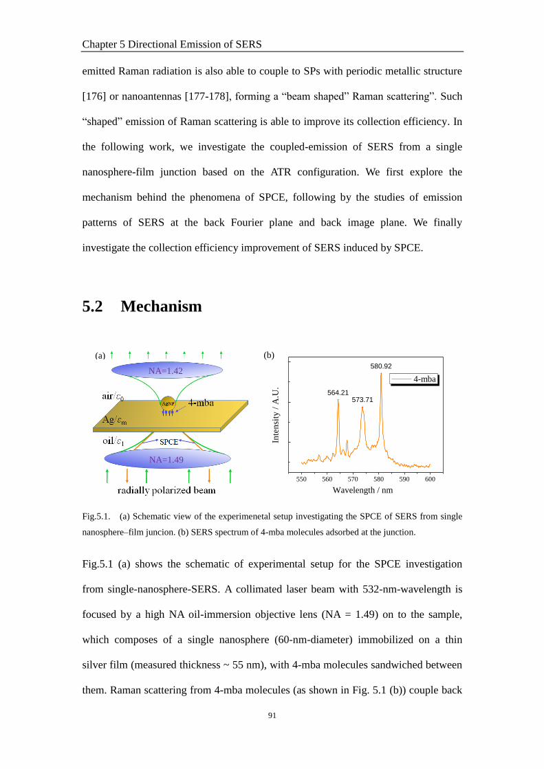
Chapter 5 Directional Emission of SERS
91
emitted Raman radiation is also able to couple to SPs with periodic metallic structure
[176] or nanoantennas [177-178], forming a “beam shaped” Raman scattering”. Such
“shaped” emission of Raman scattering is able to improve its collection efficiency. In
the following work, we investigate the coupled-emission of SERS from a single
nanosphere-film junction based on the ATR configuration. We first explore the
mechanism behind the phenomena of SPCE, following by the studies of emission
patterns of SERS at the back Fourier plane and back image plane. We finally
investigate the collection efficiency improvement of SERS induced by SPCE.
5.2 Mechanism
Fig.5.1. (a) Schematic view of the experimenetal setup investigating the SPCE of SERS from single
nanosphere–film juncion. (b) SERS spectrum of 4-mba molecules adsorbed at the junction.
Fig.5.1 (a) shows the schematic of experimental setup for the SPCE investigation
from single-nanosphere-SERS. A collimated laser beam with 532-nm-wavelength is
focused by a high NA oil-immersion objective lens (NA = 1.49) on to the sample,
which composes of a single nanosphere (60-nm-diameter) immobilized on a thin
silver film (measured thickness ~ 55 nm), with 4-mba molecules sandwiched between
them. Raman scattering from 4-mba molecules (as shown in Fig. 5.1 (b)) couple back
(a) (b)
NA=1.42
NA=1.49
550 560 570 580 590 600
564.21573.71
580.92
Inte
nsi
ty /
A.U
.
Wavelength / nm
4-mba

Chapter 5 Directional Emission of SERS
92
to SPPs at the metal surface and directionally-radiates into the substrate side with high
refractive index (the glass and oil side). The same objective lens is used to collect the
SPCE of SERS while a second objective lens (NA=1.42 but without the use of oil) is
used to collect the Raman scattering radiating directly at the transmission direction.
Fig.5.2. Three-layer system for the Fresnel coefficients calculation
For a three layer system composing of a 55-nm-thick silver film (n2) sandwiched by
semi-infinite air (n1=1) and glass (n3=1.515), as shown in Fig.5.2, the transmission
coefficient for a p-polarized beam can be calculated as following:
12 23
2 2
12 23
2 2
exp( cos )
1 exp(2 cos )
p p
p
p p
t t ik t
r r ik t
(5.1)
where tp12
and tp23
are the Fresnel transmission coefficients for each of the respective
two-layer interfaces and rp12
and rp23
the corresponding reflection coefficients. The
two-layer coefficients can be calculated with the following equations:
2 2 2
2 cos
cos sin
ij iij
p
ij i i
nt
n n
(5.2)
2 2 2
2 2 2
cos sin
cos sin
ij i iij
p
ij i i
n nr
n n
(5.3)
, 1,2; 2,3j
ij
i
nn i j
n (5.4)

Chapter 5 Directional Emission of SERS
93
where i (i=1,2) are the incident angles at each interface and are linked by the Snell’s
Law, ki the wave-vectors at each layer and t the thickness of metal film, respectively.
Fig.5.3. Transmission features of the three-layer system under different circumstances. (a) Calculated
transmittance plots against the incident angle (3) when incident light illuminates from glass into air. (b)
and (c) The transmittance plots against the incident angle (1) and transmitted angle (3), respectively,
when incident light illuminates from air into glass. Wavelength is set to be 532 nm in the calculation.
First of all, we consider that incident light is illuminating from the glass side into the
air side, passing though the thin silver film. Under this circumstance, 3 is the incident
angle while 1 is the transmitted angle. The calculated transmittance T (T=p2) plotting
against the incident angle 3 according to Eq. (5.1) is presented in Fig.5.3 (a). A sharp
transmission peak can clearly be seen around 44. This corresponds to the resonant
angle of SPPs as predicted from Eq. (2.16), and the high transmission coefficient is
the well known field enhancement effect of SPPs generated at the air-silver interface.
35 40 45 50 55
0
20
40
60
T
GlassToAir
nm
30 35 40 45 50
0
2
4
6
AirToGlass
0 45 900
1
20 20 40
%
T
0 15 30 45 60 75 900.0
0.5
1.0
1.5
2.0
T / % AirToGlass
nm
(a) (b)
(c)

Chapter 5 Directional Emission of SERS
94
Now, we consider that incident light is illuminating from air into the glass side.
Under this circumstance, 1 is the incident angle while 3 is the transmitted angle. The
calculated transmittance plotting against the incident angle 1 is illustrated in Fig.5.3
(b). As can be seen, over the whole range of available incident angles, the
transmittance is very low. This is due to the special refractive index of metal, which
has a small real part (high reflection) and a large imaginary part (high absorption).
Situation is changed if we consider it from the perspective of transmitted angle, with
the result shown in Fig.5.3 (c). It is interesting to find that a transmission peak is
present at the curve. The corresponding transmitted angle is exactly the same with that
in Fig.5.3 (a), and hence is the SPR angle. If we pick up the transmission curve at the
small angles (3 < 41.3, 41.3 is the angle for total internal reflection), as shown with
the inset, it is completely identical with that in Fig.5.3 (b), with the corresponding
angles related with the Snell’s law: n1sin(1) = n3sin(3). Hence, the transmissions at
small angles are totally due to the propagating incident radiations from the air side.
Now, we move our attention to the high transmitted angles (3 > 41.3). At SPR
angle, the transmittance is calculated to be 600%. It is more than 300 times enhanced
compared to that at small transmitted angles. Such giant enhancement is thus coming
from the evanescent radiations at the air side, which have in-plane wave-vector
component identical to that of SPPs supported at the air-silver interface and hence is
able to couple to SPPs and re-radiate into the glass side at specific angle satisfying the
wave-vector matching condition. It is therefore termed as surface plasmon coupled
-emission due to its coupled nature of the transmitted emission with surface plasmon.
As a result, it is interesting to find that: in a conventional signal collection
configuration, (for example, if the Raman signals in Fig.5.1 (a) are collected at the
upper side), the collected signals are the propagating radiations originated from the

Chapter 5 Directional Emission of SERS
95
emitters and the collection efficiency is determined by the maximum angle allowed by
the objective lens; while in an SPCE-based collection configuration, (for example, if
the Raman signals in Fig.5.1 (a) are collected at the lower side by the oil-immersion
objective lens), the collected signals are mainly from the evanescent radiations whose
in-plane wave-vector component are identical to that of SPPs and hence the collection
efficiency is determined by the radiation portion satisfying SPPs excitation condition
and the SPPs-induced field enhancement effect.
In the following sections, we will investigate the SPCE of SERS from the
perspective of Fourier plane and image plane, respectively. At the back Fourier plane,
the SPCE spectrum reflects the wave-vector information of the excited SPPs and
hence can be used for SPP characterization. At the image plane, the pattern obtained
by a CCD camera is the real-space image of the nanosphere-film junction where
4-mba molecules sit and emit the Raman signals. Since the size of nanosphere-film
junction is much smaller than that limited by the diffraction limit (0/2), Raman
scattering from a single nanosphere-film junction can be treated as a point source of
SPPs and hence the Raman image of the junction is approximate the point spread
function (PSF) of an SPCE microscopic system. We will then calculate the PSF
theoretically for the purpose of comparison.
5.3 Results
5.3.1 Fourier Plane
As can be seen in Fig.5.1 (b), the Raman spectrum of 4-mba molecules presents three
main peaks, which are 564.21 nm, 573.71 nm and 580.92 nm, respectively. Each peak
has a very narrow linewidth (1 – 2 nm). To investigate the SPCE pattern at the back

Chapter 5 Directional Emission of SERS
96
Fourier plane, we calculate for each of the above peak wavelengths the transmission
coefficients and plot them against the transmitted angle 3, with the results shown in
Fig.5.4 (a). One can see that the resonant angle slightly decreases as incident
wavelength increases.
Fig.5.4 (b) shows the back Fourier plane image of SERS from 4-mba molecules.
A bright and colorful SPCE ring is clearly seen. This corresponds to the transmission
peaks as illustrated in Fig.5.4 (a) and is due to the excitation of SPPs at the silver-air
interface, as analyzed above. The color of SPCE ring is green outside, red inside and
yellow in between, which means that the resonant angle decreases as wavelength
increases. This agrees well with the result shown in Fig.5.4 (a). The CCD camera
cannot distinguish the colors clearly because the SPR angles are very close for the
above three Raman peaks (can be seen as the picture zoomed in).
Fig.5.4. (a) Transmission coefficients of a 55-nm-thick silver film sandwiched by semi-infinite air
and glass under 564 nm, 573 nm, and 581 nm incident wavelengths, respectively. The wavelengths are
corresponding to the three main Raman peaks of 4-mba molecules. (b) Back Fourier plane image of
SERS from 4-mba molecules. The coupled-emission of SERS forms the colorful SPCE ring.
Fig.5.5 presents the pixel intensity distribution along the white dashed line in Fig.5.4
(b). The horizontal axis is set as wave-number, which is derived from the angular
information contained in the back Fourier plane image by k = k0 noil sin, where k0
is the incident wave-number in vacuum. As can be seen, the peak intensity at SPR
(b) (a)
40 42 44 46 48
0.0
0.5
1.0
1.5
2.0
2.5
532 nm
564 nm
573 nm
581 nm

Chapter 5 Directional Emission of SERS
97
angle is 55 counts along this direction and averaged 70 counts across the whole ring;
while at the non-resonant angles only the background noise is detected. The overall
counts obtained over the SPCE ring are on the order of 105, which provide strong
evidence that collection efficiency of SERS at the substrate side of the sample is
significantly increased with the help of SPCE. This is of great significance for a
system in which signals need to be collected at the substrate side, such as a
tip-enhanced Raman spectroscopy.
-14.5 -14.0 -13.5 -13.0 -12.5 -12.0 -11.5 -11.0 -10.5
0
10
20
30
40
50
60
Model: Lorentz
Equation: y = y0 + (2*A/PI)*(w/(4*(x-xc)^2 + w^2))
Chi^2/DoF = 7.6468
R^2 = 0.89828
y0 3.29475 0.33309
xc -12.4713 0.00283
w 0.10826 0.00788
A 9.09523 0.505
I
k
Fig.5.5. Pixel intensity distribution along the dashed line as shown in Fig.5.4 (b) plots against the
wave-number derived from the transmitted angle.
Another useful property of this curve is that it can be described by a Lorentzian curve
from which the FWHM encoding the propagation length of SPPs can be derived. The
fitted curve with Lorentzian function is shown in Fig.5.5 with red line. The Lorentzian
function is expressed as:
0 2 2
0
2
4( - )
A wI I
k k w
(5.5)
where w represents the FWHM of the fitted curve and is equal to 0.10826 m-1
. The
propagation length of the excited SPPs is hence 1/w, which equals to 9.237 m. For
the purpose of comparison, the propagation length derived from the transmission
curve in Fig.5.3 is 9.14 m, in line with the one measured with the SPCE ring at the

Chapter 5 Directional Emission of SERS
98
back Fourier plane. The measurement error is believed from the limited CCD pixels
near SPR angle and the background noises.
It is worth mentioning at this point that the SPCE curve from Raman scattering is
more preferred for the measurement of SPP propagation length owing to its extremely
narrow linewidth of Raman peaks compared to fluorescence. By filtering specific
Raman peak, SERS from single nanosphere-film junction can approximately serve as
a point excitation source of SPPs with single wavelength. Fluorescence spectrum, on
the other hand, has a much wider linewidth. According to Fig.5.4 (a), as incident
wavelength increases, SPR angle decreases. The eventual-transmission curve is hence
the superposition of all of the transmission curves over the spectrum of fluorescence.
This could lead to a much wider linewidth of the SPCE ring and hence a short SPP
propagation length [175, 179].
5.3.2 Image Plane
To calculate the electric field distribution at the image plane, we adopt the method
according to ref. [180]. In their general model, a point dipole on the metal-coated
glass slide is excited by a p-polarized incident plane wave as shown in Fig.5.6. The
point dipole is at a distance d away from the first interface and emits light at a
different wavelength than the excitation wavelength inc.
If we assume the electric field in the image plane is Eimage, according to ref. [180],
it can be calculated by the following equations:
4, 4, 4,( , , ) [ , , ]image r zE r z E E E (5.6)
44, 0 2 1sin cos( ) cos 2
2
I I I
r d d d
ikE K K iK (5.7)

Chapter 5 Directional Emission of SERS
99
Fig.5.6 Schematic of the imaging process within a 4f optical system of an SPCE microscope.
44, 0 2sin sin( )
2
I I
d d
ikE K K (5.8)
44, 1 0sin cos( ) 2 cos 2
2
II II
z d d d
ikE iK iK (5.9)
40 4 1 4 0 4 4 4 4 4
03
cossin ( cos cos ) ( sin )exp( cos )exp( )
cos
I
s pK J k r ik z i d
(5.10)
41 4 1 4 1 4 4 4 4 4
03
cossin sin cos ( sin )exp( cos )exp( )
cos
I
pK J k r ik z i d
(5.11)
42 4 1 4 2 4 4 4 4 4
03
cossin ( cos cos ) ( sin )exp( cos )exp( )
cos
I
s pK J k r ik z i d
(5.12)
40 4 1 4 0 4 4 4 4 4
03
cossin sin sin ( sin )exp( cos )exp( )
cos
II
pK J k r ik z i d
(5.13)
44 1 4 1 4 4 4 4 4
03
cossin cos sin ( sin )exp( cos )exp( )
cos
II
I pK J k r ik z i d
(5.14)
In these equations, Jn() denotes the Bessel function of the first kind of order n, the

Chapter 5 Directional Emission of SERS
100
maximum angle allowed by the objective lens, d the dipole orientation with respect
to z-axis, i (i=1,2,3) the incident angles at each interface and are linked by the Snell’s
Law, 4 the polar angle of the wave-vector in medium 4, the azimuthal angle of the
wave-vector, ki (i=1,2,3,4) the wave-vectors at each layer and q (q = “p” or “s”) the
Fresnel coefficients of a three-layer system for a p-polarized and s-polarized light,
respectively. As we obtain the electric field distribution, the intensity that is detected
in the image space is therefore as following:
2 2 2
4, 4, 4,(| | | | | | ) /r z TI E E E P (5.15)
where the normalization factor PT is the total power emitted by the dipole in the
presence of a metal interface.
In our SPCE experiment, Raman scattering from 4-mba molecules is excited by
the enhanced electric field at the nanosphere-film junction. On the one hand, the
effective excitation area is determined by the linewidth of electric field at the junction,
which is far below the size restricted by the diffraction limit, and hence we treat it as a
point source. On the other hand, because of the vertical orientation of the junction, a
longitudinal electric field is preferred for the excitation of localized surface plasmon.
Thus, it is also reasonable to assume that the point dipole source is vertically oriented.
In other words, d is assumed to be 0. Finally, since the nanosphere is immobilized on
the film surface, the dipole-film distance d should equal to zero. Under these
circumstances, the Raman intensity distribution at the image plane becomes:
2 2
1 04(| | | | ) /I II
TI K K P (5.16)
Fig.5.7 presents the calculated PSF of an SPCE microscopy using Eq. (5.16) and the
actual SPCE image of SERS obtained in the experiment. Incident wavelength of 573
nm was used in the calculation, which corresponds to the middle peak of the SERS

Chapter 5 Directional Emission of SERS
101
spectrum as shown in Fig.5.1 (b). It is interesting to find that the PSF of an SPCE
microscopy has the rotationally symmetric and annular-like characteristic, with
multiple rings extending out with decreasing intensity. More importantly, the PSF has
a donut shape near the center. This is not seen in the PSF of a conventional
microscopy, which has a maximum value at the center. Such unique PSF is mainly
due to the angular selection of the excitation of SPPs. The comparison between the
two figures shows a high degree of similarity in terms of their morphology (Fig.5.7
(c)).
Fig.5.7. (a) Calculated PSF of an SPCE microscopy. (b) The actual SPCE image of SERS from 4-mba
molecules obtained at the back image plane. (c) Cross-section distributions across the center of (a) and
(b), for the purpose of comparison.
Similarly, the SPCE image of Raman scattering at the back image plane is much more
accurate for characterizing the PSF of an SPCE microscopy, due to the extremely
narrow linewidth of Raman peaks. For the purpose of comparison, the PSF obtained
with fluorescence by another group is presented in Fig.5.8 [180]. One can see that
0
0.2
0.4
0.6
0.8
1
0
0.2
0.4
0.6
0.8
1
(a) (b)
-1.0 -0.5 0.0 0.5 1.0
0.0
0.2
0.4
0.6
0.8
1.0 Theoretical
Experimental
No
rmali
zed
In
ten
sity
r / m
(c)

Chapter 5 Directional Emission of SERS
102
both the locations and widths of the fringes for the experimental PSF are wider than
those of the theoretical ones, which is mainly coming from the wider linewidth of
fluorescence spectrum and hence the obtained PSF is actually the superposition of all
of the PSF at each wavelength.
Fig.5.8. PSF of an SPCE microscopy obtained with fluorescence for comparison [180].
5.4 Discussion
In our experiment (combining the experiments in Chapter 4 and Chapter 5), SPPs are
firstly excited by a tightly-focused RP beam. The SPPs subsequently interact with the
silver nanospheres on the sivler film, leading to a plasmon-hybridized gap mode with
electric field significantly enhanced at the nanosphere-film junction. The enhanced
electric field is then to excite SERS of 4-mba molecules sitting at the junction (Fig.4.9).
Due to the scattering nature of SERS, the evanescent radiation component with in-plane
wave-vector equal to kspp is able to couple back to SPPs and eventually re-radiates into
(c)

Chapter 5 Directional Emission of SERS
103
the glass side at SPR angle, forming an SPCE ring at the back Fourier plane (Fig.5.4
(b)).
Attention now paid on the role of SPPs played in our gap mode SERS system,
which is analogue to the one LSP played in a conventional SERS system. In a
conventional one, the power of enhanced Raman radiation can be calculated as [181]:
42
04
0
| || |
| |
locSERS
EP N E
E (5.17)
where N is the number of Stokes–active scatters within the hotspot, SRES the scattering
cross-section, and Eloc and E0 the amplitudes of the enhanced and incident electric field,
respectively. The contribution from LSP is illustrated with the fourth-order factor,
which is due to the enhancement of both the incident and emitted light field.
Similarly, in our system, incident light is first enhanced by the excitation of SPPs
at the silver-air interface, as illustrated with Fig.5.3 (a). The emitted Raman radiation is
finally enhanced through the SPCE, as shown in Fig.5.3 (c). The only difference arises
from their different excitation schemes. LSP can be excited with light of appropriate
frequency and polarization, irrespective of its wave-vector. Thus, the enhancement
factors for the incoming and emitted light fields are very close and hence can be
consolidated, leading to a fourth-order effect. The excitation condition for an SPP,
however, is strongly wave-vector dependent, which is illustrated with the wave-vector
matching condition (Eq. (2.16)). The additional condition results in an excitation of
SPPs with incident light and an emission of the emitted Raman scattering at fixed
angles (i.e., SPR angles) based on the ATR configuration.
Thus, the total power of Raman radiation collected can be expressed as:
42
4
| || | CE(SPCE)
| |
locSERS SPP
SPP
EP N E
E (5.18)
The fourth-order factor illustrates the enhancement induced by the plasmon-hybridized

Chapter 5 Directional Emission of SERS
104
gap mode, while the last two terms represent the enhancement from SPPs, in terms of
the SPPs excitation with incident light and collection efficiency (CE) improvement
through SPCE, respectively.
Fig.5.9. Intensity comparison between the Raman signals of R6G molecules collected at the glass
side through SPCE and collected directly at the air side (conventional). Integration time is 1s.
Collection efficiency is shown to be enhanced through SPCE.
To illustrate the collection efficiency improvement through the SPCE, we now compare
the intensity of Raman signal collected at the glass side (SPCE) to that collected at the
air side (conventional), with the result shown in Fig.5.9. The improvement of collection
efficiency can clearly be seen in Fig.5.9. The Raman intensity ratio (SPCE /
conventional) is fluctuating between 3 and 5 as we move the stage, which is because of
the non-uniform distribution of nanospheres immobilized on the metal film. Although
the collection efficiency at the air side can further be magnified by using a higher NA
objective lens, the bottom line here is that Raman signal collected via SPCE is
comparable to that collected directly at the air side.
While such improvement does not seem notable for a SERS system, it is of great
significance for a tip-enhanced Raman spectroscopy [155], in which, Raman signal is
either side-collected with a long working distance objective lens (reflection mode), or

Chapter 5 Directional Emission of SERS
105
collected at the opposite side to the metallic tip with respect to the substrate
(transmission mode). The collection efficiency under both configurations is very low.
This, however, can significantly be improved by introducing a thin metal film as the
substrate and hence SPCE occurs in the system. In addition, the SPP excitation with
incident light can also greatly improve the excitation efficiency because of its field
enhancement, as demonstrated in Eq. (5.18).
5.5 Summary
In this work, SPCE of SERS from single nanosphere-film junction was investigated.
Because of the presence of a thin silver film, Raman scattering emitted from 4-mba
molecules adsorbed at the junction is able to couple back to the SPPs and eventually
directionally-emits into the substrate side with higher refractive index. Transmission
coefficient is shown greatly enhanced at the SPR angle. It can be used to improve the
collection efficiency of Raman signals at the back side of the excitation objective lens
(SERS/TERS). Meanwhile, due to the extremely narrow linewidth of Raman peaks,
SERS from single nanosphere-film junction can be employed as a point source of
SPPs which possesses multiple single-wavelengths. By filtering specific Raman peak,
it is well-suited for the measurement of propagation length of SPPs at back Fourier
plane and quantitative characterization of PSF of an SPCE microscopy at image plane.

Chapter 6 SPP-Longitudinal-Component Detection with Single Nanoparticle SERS
106
Chapter 6 SPP-Longitudinal-Component
Detection with SERS Imaging
6.1 Chapter Introduction
In chapter 4, surface-enhanced Raman scattering from single nanosphere-film
junction excited by SPPs has been realized. In that experiment, if we scanned a
nanosphere-film junction over the propagation region of SPPs and extracted the
Raman intensity at each point, we got an intensity distribution that agrees well with
the longitudinal field component of SPPs. This intriguing result informs us that a
nanosphere-film junction attached with Raman molecules can be employed as a novel
SPP-antenna for characterizing the near-field distributions of SPPs.
As we know, an SPP has field components both in the direction perpendicular to
(longitudinal component Ez) and in the surface plane (transversal component Er), with
relative strength determined by the dielectric constants of the metal and dielectric [65].
Over the visible spectrum, the longitudinal component is much stronger than its
transversal (e.g., |Ez|2/|Er|
2 ≈ 10 and 16 for SPPs at an infinite silver-air interface at
532 nm and 633 nm incident wavelengths, respectively), and it is the longitudinal
component that is responsible for most SPPs properties. As a result, it would be more
meaningful if one can probe the longitudinal component and use it to characterize
SPPs near-field behaviour.
Over recent decades, many state-of-the-art techniques have been developed
characterizing SPPs, including fluorescence detection [56], leakage radiation
microscopy [55], near-field electrical detection [182] and near-field optical
microscopy [57-58]. The fluorescence and leakage radiation approaches are capable

Chapter 6 SPP-Longitudinal-Component Detection with Single Nanoparticle SERS
107
of performing real-time imaging of the total intensity of SPPs; however, optical
diffraction limit restricts their resolution, thus hinders a detailed analysis of SPPs.
Near-field electrical detection of SPPs is still at the single-point detection stage and
two-dimensional imaging of SPPs distributions remains challenging. NSOM is the
pivotal detection technique, which enables SPPs imaging on sub-wavelength scales by
means of a raster-scanning probe tip [42, 59-66, 68]. However, a critical issue
associated with NSOM is that typically the transversal component of an electric field
is preferentially picked up by an NSOM tip [65, 183], despite the larger contribution
of |Ez|2
to the total intensity. This jeopardizes the goal of detecting SPPs as we use a
subordinated field to characterize the SPPs behaviour. Although there are other
groups [42, 63] claiming that the detected signal of an apertured NSOM probe is
proportional to |∇⊥Ez|2, the crucial point is that there are still no experimental methods
to date that can detect directly and efficiently SPP dominant longitudinal component.
In the following work, as a continuation of chapter 4 and an important
application of my PhD project, we propose a new method to map the near-field profile
of SPPs. Our method takes advantage of SERS from a single nanosphere-film
junction where the enhancement factor is determined by the longitudinal component
of coupled SPPs between the NP and the film. By scanning the NP immobilized on
the film, we can map out the field distribution of SPP’s longitudinal component with
super-resolution.

Chapter 6 SPP-Longitudinal-Component Detection with Single Nanoparticle SERS
108
6.2 Principle
As mentioned in Chapter 4, the near-field coupling between propagating plasmon on
the metal film and localized surface plasmon of the NP in a NP-film junction system
offers a unique opportunity to extract the longitudinal component of the former
plasmon. For example, considering the plasmon virtual probe produced from focusing
a RP beam (Fig.6.1 (a)), where a plasmonic standing-wave interference pattern is
formed on the metal film, free electrons and ions will then concentrate alternatively at
the standing-wave nodes (Fig.6.1 (b)). Upon introducing a sphere-shaped NP, a
vertically-oriented gap mode is excited at the nodes by the longitudinal electric-field
of SPPs, while a laterally-aligned gap mode at the anti-nodes where the transversal
electric-field dominates (Fig.6.1 (b)).
The NP-film interaction is governed by the Coulomb interaction between the
surface charges of the localized dipolar plasmon mode on the NP and the propagating
mode at the metal surface [31]. As demonstrated in previously experimental and
theoretical work, plasmonic vertical gap mode presents a much stronger NP-film
interaction, which results in a red-shift of the resonant peak position of the vertical
mode with respect to the lateral one [31, 33, 36-37]. As a result, at a specific -incident
wavelength, the near-field enhancement factor associated with the vertical gap mode
can be much higher than the lateral mode (Fig.6.1 (c)). The enhanced electric field can
be used to boost the SERS intensity of the molecules adsorbed within the particle-film
gap. Therefore, by scanning and acquiring the SERS signals, it maps out indirectly the
field-strength of the longitudinal component (Fig.6.1 (d)).

Chapter 6 SPP-Longitudinal-Component Detection with Single Nanoparticle SERS
109
Fig.6.1. Working principe of plasmon-hybridized gap modes directed characterizaiton of SPPs (a)
Field feature of a typical SP-VP excited by a RP beam, which is essentially an evanescent Bessel-like
standing-wave. (b) Illustration of a nanosphere-film junction interacting with the longitudinal (“A”)
and transversal field (“B”) of an SPP standing wave. The longitudinal field will drive the harmonic
oscillation of free electrons inside the nanosphere perpendicular to the metal film, leadig to a
vertically-oriented plasmon-hybridized gap mode; while a lateral gap mode will be excited by the
transversal field. The different schemes of nanosphere/film interaction will result in an energy splitting
of these two kinds of plasmon-hybridized gap modes. (c) Demonstration of the mode-splitting induced
longitudinal field sensitivity. At specific incident wavelengths, field enhancement induced by the
vertical gap mode is much higher. The enhanced electric field can be used to excite SERS signal of
molecules at the nanosphere-film gap. Since the vertical gap mode contributes a higher Raman
enhancement, the intensity of SERS can be used to characterize SPPs dominant longitudinal field. (d)
Schematic diagram of plasmon-hybridized gap modes directed, SERS-based SPPs detection system.
Diagram is not to scale.
6.3 Mapping SPP Fields with SERS Imaging
We first examine the SPPs which are excited on a 45-nm-thick silver film by a
tightly-focused RP beam at a wavelength of 532 nm, under an ATR configuration with
a high NA objective lens. To create the NP-film junctions, a sub-monolayer silver
Metal
A B
Wavelength
gap mode/x gap mode/z
(a) (b)
(c) (d)

Chapter 6 SPP-Longitudinal-Component Detection with Single Nanoparticle SERS
110
nanosphere of 60-nm-diameter was self-assembled on the silver film by the thiol pairs
of 4-mercaptobenzoic acid (4-mba) molecules sandwiched between them, which were
also employed as the Raman probe of the evanescent surface plasmon fields. We have
chosen this type of molecules because of their non-fluorescent nature which avoids
the uncertainty induced by fluorescence such as “quenching effect”.
Fig.6.2. Mapping an SP-VP with SERS imaging. (a) Measured near-field distribution of plasmon
virtual probe produced by a tightly-focused RP beam, compared with its calculated longitudinal (b) and
transversal (c) electric field components. (d) Cross-section distribution comparison between the
measured virtual probe and calculated longitudinal field component. (e) Statistical measurement of the
central spot size of plasmon virtual probe with 50 randomly-selected nanospheres on the metal film,
verifying the accuracy and reproducibility of our measurement. Incident wavelength is 532nm. Area of
contour maps is 4 m 4 m.
The mapping of SPP standing-wave pattern is presented in Fig.6.2 (a), which is
obtained by raster scanning the nanosphere-film junction over the propagation region
of SPPs and recording the intensity of SERS at each point. Because of the full beam
p-polarization of a RP beam, SPPs can be excited along all azimuthal directions thus
to form a sub-diffraction-limited evanescent plasmon virtual probe at the center. As
-1 0 10.0
0.2
0.4
0.6
0.8
1.0
Calculated
FWHM:185nm
Measured
Inte
nsi
ty
Lateral Positon / m
Calculated |Ez|2
Calculated |Er|2 Measured
0 10 20 30 40 50100
120
140
160
180
200
FW
HM
/ n
m
Number
Calculated
176 184 192 2000
5
10
15
nm
cou
nts
(a)
(d)
(b) (c)
(e)

Chapter 6 SPP-Longitudinal-Component Detection with Single Nanoparticle SERS
111
can be seen, the measured pattern is in excellent agreement with the calculated
longitudinal component (Fig.6.2 (b)). Note that this result opposes to the transversal
field distribution as shown in the calculation (Fig.6.2 (c)) which is the usual pattern
obtained by NSOM. The agreement can be assessed quantitatively by plotting the
intensity curves across the center (Fig.6.2 (d)).
The size of the center spot can be extracted subsequently. The result from 50
randomly-selected nanospheres is presented in Fig.6.2 (e). As shown, the measured
spot sizes approximately follow a normal distribution (see the inset) with mean value
of 188.93 nm (0.355λ0) and standard deviation of 6.76 nm. The slight deviation from
the theoretical value (185 nm) should attribute to the finite scanning step size (40nm).
Both of the excellent agreement in the mean value and the small standard deviation
indicate a high reproducibility as well as high accuracy of our measurement. To the
best of our knowledge, this is the first direct measurement of the spot size of SP-VP in
the visible range.
Fig.6.3 (a-c) present the mappings correspond to other typical polarized-beams
including a tightly-focused linearly polarized Gaussian beam, a circularly polarized
beam, and a linearly polarized optical-vortex beam of charge “1” [184], respectively.
These measured results, on the one hand, verify further the longitudinal field
sensitivity of our method; and on the other hand, also explicitly illustrate the
capability of a RP beam to form the plasmon virtual probe owes to its properties of
full beam p-polarization and in-phase plasmon excitation. This capability is missed
for the other beams either because of the spatially-variant p-polarization (for Fig.6.3
(a), (c)) or because of out-of-phase SPPs excitation (for Fig.6.3 (a), (b)). This also
verifies that a tightly-focused RP beam can be as the optimized source for the NP-film
junction configuration.

Chapter 6 SPP-Longitudinal-Component Detection with Single Nanoparticle SERS
112
Fig.6.3 The mapping of SPP patterns under a tightly-focused linearly polarized Gaussian beam
(LPGB), a circularly polarized beam (CPB) and a linearly polarized optical-vortex beam (LPVB) of
charge “1”, respectively, to verify further the longitudinal field sensitivity of our method and show the
distinct SPP patterns under different incident polarizations. From top to bottom: measured, calculated
|Ez|2 and calculated |Er|
2, respectively. From left to right: LPGB, CPB and LPVB, respectively. Area of
contour maps is 4 m 4 m. Incident wavelength is 532 nm.
Compared to the current widely-used NSOM system, our method shows advantages in
many aspects. First of all, by making use of the energy spitting of plasmon-hybridized
gap modes and SERS imaging, the strongly dominant longitudinal surface plasmon
fields are detected. While for a NSOM system, it was demonstrated, from both
experiment and theoretical calculation, that the current commercially-available
NSOM tip is more sensitive to the transversal electric field in the visible range. For a
direct comparison, the counterpart of measurements for all of the above polarizations
LPGB-Calculated |Ez|2
LPGB-Calculated |Er|2
CPB-Calculated |Ez|2
CPB-Calculated |Er|2
LPVB-Calculated |Ez|2
LPVB-Calculated |Er|2
LPGB-Measured CPB-Measure
d
LPVB-Measured
(a) (b) (c)
(d) (e) (f)
(g) (h) (i)

Chapter 6 SPP-Longitudinal-Component Detection with Single Nanoparticle SERS
113
by NSOM can be found respectively in Refs. [42, 63, 68] (as shown in Fig.6.4), where
the measured patterns coincide with those of the transversal components, even if
intensities of longitudinal components are 16 times (as calculated by |εm|/εd) [65]
stronger under 632 nm incident wavelength for silver film as used in their work.
Fig.6.4. Comparison of SPPs distribution obtained with NSOM [42, 63, 68] (top) and our SERS
imaging (bottom). From left to right: linearly polarized Gaussian beam, radially polarized beam, and
linearly polarized optical vortex beam, respectively.
Secondly, the influence from transmitted light is significantly suppressed, which is
clearly shown in Fig.4.9. The transmitted light shows a great influence on the
conventional plasmon detection techniques, particularly for the method with
direct-detection scheme such as aperture-type NSOM. For an aperture-less-type
NSOM system, the collection signal is generally the Rayleigh scattering from metallic
tip. Although Rayleigh scattering possesses a large scattering cross-section, its
wavelength is exactly the same with the illuminating wavelength and hence is hardly
extracted from the incident light. Raman scattering, on the contrary, shows a small
wavelength shift with respect to the illuminating one. It can easily be extracted by
using a notch (or long-pass) filter. Meanwhile, because of the excitation of

Chapter 6 SPP-Longitudinal-Component Detection with Single Nanoparticle SERS
114
plasmon-hybridized gap mode, Raman scattering can significantly be enhanced by
more than 108 for a NP-film junction excitation scheme. This greatly compensates for
the small cross-section of normal Raman scattering. Finally, the turbulence induced
by the SP-antenna in our method is much smaller than that induced by the NSOM tip.
This is, on the one hand, because of the smaller size of nanosphere (can be less than
50 nm) than that of NSOM tip (typically more than 50 nm); on the other hand,
localized plasmon will be excited at the metallic NSOM tip-end, which complicates
the detected signals. In our method, localized plasmon is utilized to generate the
longitudinal field sensitivity and to enhance the Raman scattering and hence the
turbulence from it does not exist.
6.4 Numerical-Modelling with FDTD Method
In order to obtain the responses of a nanosphere-film junction to SPPs’ longitudinal
and transversal field, we place the nanosphere at the node (point “A” in Fig.6.1 (b))
and anti-node (point “B” in Fig.6.1 (b)) of SPP standing-wave respectively and carry
out a wavelength scan. The simulated result is shown in Fig.6.5 (a), with vertical axis
representing the normalized maximum electric field at the nanosphere-film gap. It is
seen that both the resonant wavelength of lateral (480 nm) and vertical (500 nm) gap
mode show remarkable red-shift with respect to the nanosphere standing on a glass
substrate (410 nm), because of the Coulomb interaction between the nanosphere and
silver film. However, the red-shift of vertical gap mode is more notable due to the
stronger interaction. This can clearly be seen in Fig.6.5 (b) and Fig.6.5 (c), which give
the electric field vectorial distributions in the vicinity of nanosphere under resonant
conditions of lateral and vertical gap mode, respectively.

Chapter 6 SPP-Longitudinal-Component Detection with Single Nanoparticle SERS
115
Fig.6.5. Numerical-modelling of a nanosphere-film junction interacting with SP-VP. (a) Normalized
maximum electric field at the nanosphere-film junction plots against the wavelength, when the
nanosphere placed at the standing wave node (point “A” in Fig.6.1 (b), vertical gap mode), anti-node
(point “B” in Fig.6.1 (b), lateral gap mode), and on a glass substrate, respectively. (b) and (c) Electric
field vectorial distribution in the vicinity of nanosphere-film gap, in the case of lateral and vertical gap
mode, respectively. (d) Calculated averaged Raman enhancement for each mode, which is employed to
evaluate the field sensitivity of a NP-film junction. Left vertical axis is set as log10(RE).
In the case of lateral gap mode, electric field generally travels horizontally inside the
nanosphere and bends to the metal surface gradually because of the attraction between
the lateral sides of nanosphere and the metal surface. It is just opposite to the case of
vertical gap mode, under which the electric field insider the nanosphere travels
vertically and the Coulomb attraction occurs between the lower side of nanosphere
and the adjacent metal surface. This leads to a much higher concentration of electrons
near the junction and a tighter interaction volume, both of which indicate a stronger
nanosphere-film interaction.
400 480 560 640 720
6
7
8
9
0
4
8
12
16 REz
REr
RE
/ nm
RE
z/RE
r
360 420 480 540 600 660 720
0.0
0.2
0.4
0.6
0.8
1.0
nm
Max
(|E
|2)
lateral
vertical
glass
0 5 10 15 20 25 300
5
10
15
20
25
30
0 5 10 15 20 25 300
5
10
15
20
25
30
(a) (d)
(b) (c)

Chapter 6 SPP-Longitudinal-Component Detection with Single Nanoparticle SERS
116
Fig.6.6. Contour maps of electric field distribution. (a) and (b) Vertical and lateral gap mode in the
XZ plane. (c) and (d) The corresponding modes in the nanosphere-film gap plane, respectively.
Colorbar scale is set as log10(|E|2). The arrows represent the electric field orientation of SP-VP in the
absence of nanosphere. Incident wavelength is 532 nm.
The field distribution of each mode is illustrated in Fig.6.6. For both cases, the electric
field is strongly concentrated at the nanosphere-film gap (Fig.6.6 (a) and Fig.6.6 (b)),
but is much confined and hence a higher field enhancement for the vertical gap mode.
In the horizontal gap plane, the pattern is axial-symmetric for the vertical gap mode
(Fig.6.6 (c)), while it is dipolar-like for the lateral (Fig.6.6 (d)), with mode orientation
parallel to the polarization of electric field in the absence of nanosphere. The mode
disparity also indicates a higher nanosphere-film interaction for the vertical gap mode
owing to its larger effective interaction area.
Raman enhancement (RE), the parameter to evaluate the field sensitivity of a
NP-film junction, can be calculated thereafter by the following expression:
4
SPP 2 SPP 2
SPP 4,
| || | / | |
| |
loc
ij
p ij p
i j ij
ERE E E
E
(6.1)
in which Eijloc
denotes the localized electric field amplitude at the horizontal gap plane,
-0.04 0 0.04
-0.04
0
0.04
3
4
5
6
-0.1 0 0.1
-0.1
0
0.1
2
3
4
5
6
7
-0.1 0 0.1
-0.1
0
0.1
1
2
3
4
5
6
-0.04 0 0.04
-0.04
0
0.04
4
5
6
7(d)
(b)
(c)
(a)

Chapter 6 SPP-Longitudinal-Component Detection with Single Nanoparticle SERS
117
EijSPP
the amplitude of SPP in the absence of nanosphere, and p (“z” or “r”) represents
the excitation longitudinal or transversal electric field, respectively. The calculated RE
plotting against the wavelength is shown in Fig.6.5 (d). One can see that the
nanosphere-film junction doesn’t exhibit a uniform response over the visible range, i.e.
it is sensitive to the transversal field in the shorter wavelength range because of the
lateral gap mode, and turns into the longitudinal field sensitivity gradually as incident
wavelength increases. The extent of longitudinal field sensitivity is determined by
three factors: the magnitude of red-shift of vertical gap mode with respect to the
lateral; their relative peak RE (i.e. max(REz)/max(REr), depending on the field
enhancement and mode pattern), and their relative mode losses, respectively, with the
first one making the major contribution. Although the longitudinal field sensitivity at
longer wavelengths is at the expense of RE, as can be seen in Fig.6.5 (d), the RE is
still higher enough for the excitation of Raman signals and hence for the measurement
of SPPs. Meanwhile, by carefully designing the structural parameters of NP-film
junction (e.g., the size, shape, and composition of NP), one can tune the resonant
wavelength of gap modes to reach an optimized balance between RE and longitudinal
field sensitivity at each incident wavelength.
6.5 Summary
In conclusion, we have reported a novel method to directly and accurately map the
dominant longitudinal component of SPPs. The method relies on the longitudinal field
component preferentially exciting LSP and enhancing the electric field in SPCM.
Meanwhile, the adverse influences from transmitted and scattering light are
significantly suppressed because of the relatively low Raman enhancement compared
with that arising from SPPs, leading to an extremely clean and pure SPP detection.

Chapter 6 SPP-Longitudinal-Component Detection with Single Nanoparticle SERS
118
Worth mentioning is the point that SPCM is not limited to SPP detection under
tightly-focused configurations. As long as the nanosphere can be replaced with a
Raman probe attached metallic tip and equipped with a feedback circuit (analogous to
tip-enhanced Raman spectroscopy[185]), it can be extended to detect SPPs excited
under any type of configuration. We believe that SPCM, in combination with NSOM,
will provide a deeper and more complete understanding of SPP behaviour and open
new developments in SPP-based applications.
Experimental apparatus: An Olympus oil immersion objective lens (60 x, NA=1.49)
was used to focus the collimated incident beam on to the silver-air interface to excite
the SPPs. Raman images of immobilized Ag nanospheres on Ag film were captured
with a Thorlabs digital CCD camera. Meanwhile, Raman signals emitted from 4-mba
molecules located at the nanosphere-film junction were obtained with an OceanOptics
TEC cooling spectrometer (QE 65000). A piezo-scanning stage (Physikinstrumente
(PI), P545.3R7) was applied initially to position the nanosphere at the centre of focal
plane, by monitoring the intensity of Raman signals from spectrometer and CCD
camera, and subsequently to raster scan the nanosphere over the SPP region to get the
near-field SPP distribution.
SPP mapping and measurement: After an isolated individual nanosphere was found
(checked with a CCD camera) and positioned at the centre of focal plane, Raman
signals emitted from 4-mba molecules were sent for further amplification to a
Hamamatsu photomultiplier tube (PMT), instead of the spectrometer. The PI scanning
stage, the acquisition of data from the PMT, and real-time displaying of SPP
distribution were all realized and coordinated via Labview software, as shown in
Fig.6.7. For two-dimensional mappings, the scanning range and step size were set to 5

Chapter 6 SPP-Longitudinal-Component Detection with Single Nanoparticle SERS
119
μm × 5 μm and 50 nm respectively; for SPP spot-size measurements, the scanning
range in the X direction was set at 400 nm to trace the cross-section distribution
across the centre, and that for the Y direction was set to 4 μm for the actual
measurements. The step size for both directions was set to 40 nm.
Fig.6.7. Front view of the Labview program coded for two-dimensional mapping of SPP’s
longitudinal component.

Chapter 7 Conclusion and Future Works
120
Chapter 7 Conclusions and Future Works
7.1 Conclusions
In this thesis, we proposed a multi-functional surface-enhanced Raman system and
investigated it both from simulation and experiment. Our system is based on a novel
idea, which employs the fascinating electromagnetic enhancement stemming from the
SPP&LSP coupling mode (plasmon-hybridized mode), and deals with the limitations/
problems facing with the current SERS and other plasmon-based techniques.
First, with surface-enhanced Raman spectroscopy, electromagnetic enhancement
from SP coupling mode was proved to be much superior to that from separate modes.
Raman enhancement of 109 - 10
10 has been achieved numerically. Meanwhile, the
existence of SPCE in the presence of a thin metal film leads to a directional emission
of SERS, which is able to improve the collection efficiency of Raman signals.
Moreover, the reproducibility of NP-film junctions is verified much higher than that
of inter-particle junction (dimer structure). Hence, from the perspective of the balance
among Raman enhancement, collection efficiency and reproducibility, our
plasmon-hybridized mode system is of great potential as a robust SERS substrate.
Both air and water can be as the environment for the specimens in our system. The
specimens should have a small thickness (<10 nm) because the field enhancement
from a NP-film junction strongly depends on the separation between the NP and metal
film. Gases can also be the specimens in our system.
Secondly, the SPCE spectrum obtained at the back Fourier plane contains optical
parameter information of the excited SPPs. In particular, the wave-numbers and
propagation length can rapidly be extracted from the SPCE ring without any
mechanical movement or angle scanning. Although the SPCE spectrum from

Chapter 7 Conclusion and Future Works
121
fluorescence has been employed for the measurement of propagation length of SPPs
before, the advantages of using SERS is prominent, due to the extremely narrow
bandwidth of Raman peaks, small physical size of NP-film junction and avoidance of
using a thin dielectric layer as a spacer.
Finally, a direct and efficient detection of the dominant longitudinal component
of SPPs is realized based on our plasmon-hybridized mode system, which takes
advantage of SERS from a single NP-film junction where the enhancement factor is
determined by the longitudinal component of coupled SPPs between the NP and the
film. The proposed technique tackles the problems associated with conventional
NSOM system. It gives rise to the state-of-the-art near-field measurement with
comparative advantages including:
(i) Direct longitudinal component detection. To our best knowledge, this is the first
technique which can directly and efficiently detect the SPPs dominant
longitudinal component.
(ii) Super-resolution. A resolution of less than 50 nm can be achieved.
(iii) Less influence from transmitted and scattered light.
(iv) Less turbulence induced by the probe.
(v) Quantitative analysis. As an example, we measured for the first time the size of a
sharply-confined SPP spot under a tightly-focused RP beam excitation. Such a
measurement is a puzzle for a long time because of the drawbacks of NSOM
system and lack of alternative approaches.

Chapter 7 Conclusion and Future Works
122
7.2 Future Works
7.2.1 Surface Plasmon Virtual Probe Directed Tip-enhanced
Raman Spectroscopy
(a) High sensitivity, multi-functional tip-enhanced Raman System
Another attractive usage of surface plasmon virtual probe is as the excitation source
for tip-enhanced Raman spectroscopy (TERS). TERS is a derivative application from
surface-enhanced Raman spectroscopy, in which a NP is replaced with a metallic tip,
equipped with a feedback circuit to keep the tip-sample distance constant, such as an
AFM head or STM head. By raster scanning the tip over the sample and extracting the
Raman spectrum at each point, a spectroscopic image of the detected sample can be
generated with sub-diffraction limit resolution. This is one of the most intriguing
advantages of TERS.
Fig.7.1. High sensitivity, high resolution tip-enhanced Raman spectroscopy based on surface plasmon
virtual probe and surface plasmon coupled-emission.
Since the metallic tip of an AFM head is always vertically-oriented, as shown in
Fig.7.1, a longitudinal electric field component is intrinsically required. General
approach in the past is using a tightly focused linearly polarized beam, in which two

Chapter 7 Conclusion and Future Works
123
longitudinal field lobes is formed around the centre of focal plane. However, this
method suffers from the efficiency problem because the longitudinal field in the focal
plane is generally a subordinated component and hence the utility of power is low.
Surface plasmon virtual probe is just different. On the one hand, as mentioned
in chapter 6, the relative strength of z-component over r-component of an SPP is
determined by the dielectric constants of the metal and dielectric[65]. Over the visible
spectrum, the longitudinal component is much stronger than its transversal, and so
does for an SP-VP. This significantly improve the incident power utility while
suppress the background noise induced by the transversal component. On the other
hand, just as did and proved in our previous experiments, the coupling between the
SPPs and LSP could result in a much higher Raman enhancement compared to that
from separate mode. It is exactly the same as we employ the SP-VP as the excitation
source for TERS. Furthermore, SPCE from tip-enhanced Raman scattering will occur
as well in the presence of a thin metal film. This will greatly improve the collection
efficiency of a TERS system because Raman signals need to be collected at the back
side of objective lens. Finally, as discussed in the conclusion section in chapter 6, as
long as the nanosphere can be replaced with a Raman probe attached metallic tip and
equipped with a feedback circuit, our SPP detection technique can be extended to
detect the SPPs excited under any type of configuration. This is readily realized as we
introduce the AFM head into our previous system.
Taking all of these unique properties into account, the introduction of an AFM
head into our previous system will lead to a SP-VP directed high sensitivity
tip-enhanced Raman system, which is, at the same time, capable of realizing the
super-resolution spectroscopic imaging of physical samples and super-resolution
near-field imaging of SPP’s longitudinal component.

Chapter 7 Conclusion and Future Works
124
(b) Controllable inter-particle junction excited by SP-VP
The dimer structure is widely accepted to generate the greatest Raman enhancement,
owing to the strong coupling between the LSP modes on each particle. However, the
nature of random formation of inter-particle junction makes it quite irreproducible,
causing Raman enhancement with dramatic variations. This great restricts its practical
applications. Bearing this situation in mind and continuing the work in part (a), if we
immobilize an individual metal nanosphere on the thin silver film and accurately
move it just under the AFM metallic tip, a vertically-oriented inter-particle junction is
formed, and entirely under control, just as shown in Fig.7.2.
Fig.7.2. Controllable vertically-oriented dimer structure based on AFM tip, excited by an SP-VP
Since the inter-particle junction is vertically-oriented, an SP-VP could be a great
candidate for the excitation of LSP under this circumstance because of its dominant
longitudinal component. More interestingly, an SPP-LSP-LSP coupling mode will be
generated. This could further improve the Raman enhancement compared to
conventional inter-particle junction excited by propagating radiation, which is proved
by the preliminary result as shown in Fig.7.3. Similarly, the existence of SPCE from
Raman scattering will greatly improve the collection efficiency of such TERS-based

Chapter 7 Conclusion and Future Works
125
inter-particle system at the back side of objective lens. Since this structure and surface
plasmon hybrid mode system is entire new, there should be more interesting
phenomena behind this and hence a systematic investigation is necessary and quite
meaningful. In particular, how the dimer structure responses to the SP-VP and to what
extent the Raman enhancement could be improved are worthy studying.
Fig.7.3. Near-field distribution around a vertically-oriented dimer structure excited by a surface
plasmon virtual probe, with 480 nm incident wavelength. The white scale bar represents 100 nm.
7.2.2 All-in-one Surface & Tip-enhanced Raman System
Our ultimate objective is to build up an all-in-one surface & tip-enhanced Raman
system, which consolidates all of the functionalities mentioned previously into an
integrated system. The schematic of such all-in-one system is presented in Fig.7.4.
From the setup point of view, it has three main parts:
(a) Light Source, including a 532 CW laser, an optical valve (LP + HW), a polarization
converter and a beam expander. It is used to generate and expand a RP beam.
(b) Excitation part, composing of a high NA objective lens, a piezo-scanning stage, an
AFM tip or nanosphere. SP-VP will be generated and employed as the excitation
102
103
104
105
106
107

Chapter 7 Conclusion and Future Works
126
source to interact with optical antennas, such as nanosphere-film junction, AFM
tip, etc.
(c) Collection part, which consists of CCD cameras, spectrometer and PMT, to collect
the Raman signals with the help of SPCE.
Fig.7.4. Schematic view of an all-in-one surface-enhanced Raman system. HW: half waveplate; LP:
linear polarizer; BS: beam splitter; BFP: back Fourier plane; IP: image plane; Spec: spectrometer; PC:
personal computer; NS: nanosphere.
From the perspective of functionality:
(a) When single NP is used. Firstly, it can be as a robust substrate for SERS (high
Raman enhancement, high reproducibility, and high collection efficiency).
Secondly, it can be used as a convenient tool for measurement of SPP’s
propagation length by analyzing the SPCE ring obtained at the back Fourier plane.
Finally, it can be used to map the longitudinal component distribution of SPPs. In
particular, an SP-VP will be imaged and used as the excitation source for our
system.

Chapter 7 Conclusion and Future Works
127
(b) When the AFM tip is used. It can be used as an SP-VP directed high sensitivity
tip-enhanced Raman system, which is, at the same time, capable of realizing the
super-resolution spectroscopic imaging of physical samples and super-resolution
near-field imaging of longitudinal component of SPPs excited under any kinds of
configurations.
(c) When AFM tip and NP are used together. A controllable vertically-oriented dimer
structure is formed and excited by an SP-VP. The giant Raman enhancement is of
high potential to realize the single molecule fingerprint detection.

Authors Publications
128
Authors Publications
Journal papers:
1. L. P. Du, X. J. Zhang, T. Mei, and X. C. Yuan, "Localized surface plasmons,
surface plasmon polaritons, and their coupling in 2D metallic array for SERS,"
Opt. Express 18, 1959-1965 (2010).
2. L. P. Du, G. H. Yuan, D. Y. Tang, and X. C. Yuan, "Tightly focused radially
polarized beam for propagating surface plasmon-assisted gap-mode Raman
spectroscopy," Plasmonics 6, 651-657 (2011).
3. L. P. Du, D. Y. Tang G. H. Yuan, S. B. Wei and X. C. Yuan, “Emission pattern
of surface enhanced Raman scattering from single nanoparticle-film junction,”
Appl. Phys. Lett 102, 081117 (2013). (2013).
4. L. P. Du, D. Y. Lei, G. H. Yuan, H. Fang, X. Zhang, Q. Wang, D. Y. Tang, C. J.
Min, S. A. Maier and X. C. Yuan, “Mapping plasmonic near-field profiles and
dynamics by Surface-enhanced Raman scattering,” communicated (2013).
5. L. P. Du, D. Y. Tang and X. C. Yuan, “Film-driven plasmon hybridization on a
nanoparticle-film junction system,” in preparation (2013).
6. L. P. Du, D. Y. Tang and X. C. Yuan, “Launching structureless plasmon lenses
with focused radially polarized beam,” in preparation (2013).
7. S. B. Wei, J. Lin, Q. Wang, G. H. Yuan, L. P. Du, R. Wang, L. Xu, M. H. Hong
and X. C. Yuan, “Singular diffraction-free surface plasmon beams,” Opt. Lett,
accepted (2013).
Conferences:
1. L. P. Du, D. Y. Tang and X.-C. Yuan “Radially polarized beam induced
plasmon-hybrid-mode for surface-enhanced Raman spectroscopy” International
Conference on Nanophotonics, Beijing, (2012)
2. L. P. Du, D. Y. Tang and X.-C. Yuan “Theoretically modeling of tip-enhanced
Raman scattering under linearly and radially polarized beam with DDA method”
Advances in Optoelectronics & Micro/nano-optics, Guangzhou, (2010)

References
129
References
1. C. V. Raman, "A change of wave-length in light scattering," Nature 121, 619-619
(1928).
2. S. M. Nie and S. R. Emery, "Probing single molecules and single nanoparticles by
surface-enhanced raman scattering," Science 275, 1102-1106 (1997).
3. Fleischm.M, P. J. Hendra, and McQuilla.Aj, "Raman-spectra of pyridine adsorbed at a
silver electrode," Chem. Phys. Lett. 26, 163-166 (1974).
4. K. Kneipp, Y. Wang, H. Kneipp, L. T. Perelman, I. Itzkan, R. Dasari, and M. S. Feld,
"Single molecule detection using surface-enhanced raman scattering (SERS)," Phys.
Rev. Lett. 78, 1667-1670 (1997).
5. A. Otto, I. Mrozek, H. Grabhorn, and W. Akemann, "Surface-enhanced
raman-scattering," J. Phys-Condens. Mat. 4, 1143-1212 (1992).
6. M. Moskovits, "Surface-enhanced raman spectroscopy: A brief retrospective," J. Raman.
Spectrosc. 36, 485-496 (2005).
7. J. I. Gersten, "The effect of surface-roughness on surface enhanced raman-scattering," J.
Chem. Phys. 72, 5779-5780 (1980).
8. M. Moskovits, "Surface-enhanced spectroscopy," Rev. Mod. Phys. 57, 783-826 (1985).
9. K. L. Kelly, E. Coronado, L. L. Zhao, and G. C. Schatz, "The optical properties of
metal nanoparticles: The influence of size, shape, and dielectric environment," J. Phys.
Chem. B 107, 668-677 (2003).
10. K. A. Willets and R. P. Van Duyne, "Localized surface plasmon resonance spectroscopy
and sensing," Annu. Rev. Phys. Chem. 58, 267-297 (2007).
11. M. P. Pileni, "Control of the size and shape of inorganic nanocrystals at various scales
from nano to macrodomains," J. Phys. Chem. C. 111, 9019-9038 (2007).
12. W. H. Yang, G. C. Schatz, and R. P. Vanduyne, "Discrete dipole approximation for
calculating extinction and raman intensities for small particles with arbitrary shapes," J.
Chem. Phys. 103, 869-875 (1995).
13. E. Hao and G. C. Schatz, "Electromagnetic fields around silver nanoparticles and
dimers," J. Chem. Phys. 120, 357-366 (2004).
14. G. C. Schatz, M. A. Young, and R. P. Van Duyne, "Electromagnetic mechanism of
sers," Surface-Enhanced Raman Scattering: Physics and Applications 103, 19-45
(2006).
15. C. E. Talley, J. B. Jackson, C. Oubre, N. K. Grady, C. W. Hollars, S. M. Lane, T. R.
Huser, P. Nordlander, and N. J. Halas, "Surface-enhanced raman scattering from
individual Au nanoparticles and nanoparticle dimer substrates," Nano. Lett. 5,

References
130
1569-1574 (2005).
16. F. Svedberg, Z. P. Li, H. X. Xu, and M. Kall, "Creating hot nanoparticle pairs for
surface-enhanced raman spectroscopy through optical manipulation," Nano. Lett. 6,
2639-2641 (2006).
17. B. Vlckova, M. Moskovits, I. Pavel, K. Siskova, M. Sladkova, and M. Slouf,
"Single-molecule surface-enhanced raman spectroscopy from a molecularly-bridged
silver nanoparticle dimer," Chem. Phys. Lett. 455, 131-134 (2008).
18. T. Dadosh, J. Sperling, G. W. Bryant, R. Breslow, T. Shegai, M. Dyshel, G. Haran, and I.
Bar-Joseph, "Plasmonic control of the shape of the raman spectrum of a single
molecule in a silver nanoparticle dimer," Acs Nano 3, 1988-1994 (2009).
19. J. M. McMahon, A. I. Henry, K. L. Wustholz, M. J. Natan, R. G. Freeman, R. P. Van
Duyne, and G. C. Schatz, "Gold nanoparticle dimer plasmonics: Finite element method
calculations of the electromagnetic enhancement to surface-enhanced raman
spectroscopy," Anal. Bioanal. Chem. 394, 1819-1825 (2009).
20. A. M. Michaels, J. Jiang, and L. Brus, "Ag nanocrystal junctions as the site for
surface-enhanced raman scattering of single rhodamine 6G molecules," J. Phys. Chem.
B 104, 11965-11971 (2000).
21. A. M. Michaels, M. Nirmal, and L. E. Brus, "Surface enhanced raman spectroscopy of
individual rhodamine 6G molecules on large Ag nanocrystals," J. Am. Chem. Soc. 121,
9932-9939 (1999).
22. J. W. Zheng, Y. G. Zhou, X. W. Li, L. Ji, T. H. Lu, and R. A. Gu, "Surface-enhanced
raman scattering of 4-aminothiophenol in assemblies of nanosized particles and the
macroscopic surface of silver," Langmuir 19, 632-636 (2003).
23. G. Braun, S. J. Lee, M. Dante, T. Q. Nguyen, M. Moskovits, and N. Reich,
"Surface-enhanced raman spectroscopy for DNA detection by nanoparticle assembly
onto smooth metal films," J. Am. Chem. Soc. 129, 6378-+ (2007).
24. M. K. Kinnan and G. Chumanov, "Surface enhanced raman scattering from silver
nanoparticle arrays on silver mirror films: Plasmon-induced electronic coupling as the
enhancement mechanism," J. Phys. Chem. C. 111, 18010-18017 (2007).
25. K. Kim and J. K. Yoon, "Raman scattering of 4-aminobenzenethiol sandwiched
between Ag/Au nanoparticle and macroscopically smooth Au substrate," J. Phys. Chem.
B. 109, 20731-20736 (2005).
26. J. K. Daniels and G. Chumanov, "Nanoparticle-mirror sandwich substrates for
surface-enhanced raman scattering," J. Phys. Chem. B. 109, 17936-17942 (2005).
27. W. H. Park, S. H. Ahn, and Z. H. Kim, "Surface-enhanced raman scattering from a
single nanoparticle-plane junction," Chemphyschem 9, 2491-2494 (2008).
28. K. Ikeda, N. Fujimoto, H. Uehara, and K. Uosaki, "Raman scattering of aryl isocyanide

References
131
monolayers on atomically at Au(111) single crystal surfaces enhanced by gap-mode
plasmon excitation," Chem. Phys. Lett. 460, 205-208 (2008).
29. P. Nordlander and F. Le, "Plasmonic structure and electromagnetic field enhancements
in the metallic nanoparticle-film system," Appl. Phys. B-Laser. O. 84, 35-41 (2006).
30. C. J. Orendorff, A. Gole, T. K. Sau, and C. J. Murphy, "Surface-enhanced raman
spectroscopy of self-assembled monolayers: Sandwich architecture and nanoparticle
shape dependence," Anal. Chem. 77, 3261-3266 (2005).
31. P. Nordlander and E. Prodan, "Plasmon hybridization in nanoparticles near metallic
surfaces," Nano. Lett. 4, 2209-2213 (2004).
32. F. Le, N. Z. Lwin, N. J. Halas, and P. Nordlander, "Plasmonic interactions between a
metallic nanoshell and a thin metallic film," Phys. Rev. B 76(2007).
33. J. J. Mock, R. T. Hill, A. Degiron, S. Zauscher, A. Chilkoti, and D. R. Smith,
"Distance-dependent plasmon resonant coupling between a gold nanoparticle and gold
film," Nano. Lett. 8, 2245-2252 (2008).
34. M. W. Knight, Y. P. Wu, J. B. Lassiter, P. Nordlander, and N. J. Halas, "Substrates
matter: Influence of an adjacent dielectric on an individual plasmonic nanoparticle,"
Nano. Lett. 9, 2188-2192 (2009).
35. M. Hu, A. Ghoshal, M. Marquez, and P. G. Kik, "Single particle spectroscopy study of
metal-film-induced tuning of silver nanoparticle plasmon resonances," J. Phys. Chem.
C. 114, 7509-7514 (2010).
36. N. Yamamoto, S. Ohtani, and F. J. G. de Abajo, "Gap and mie plasmons in individual
silver nanospheres near a silver surface," Nano Lett. 11, 91-95 (2011).
37. D. Y. Lei, A. I. Fernandez-Dominguez, Y. Sonnefraud, K. Appavoo, R. F. Haglund, J. B.
Pendry, and S. A. Maier, "Revealing plasmonic gap modes in particle-on-film systems
using dark-field spectroscopy," Acs Nano 6, 1380-1386 (2012).
38. B. Sick, B. Hecht, and L. Novotny, "Orientational imaging of single molecules by
annular illumination," Phys. Rev. Lett. 85, 4482-4485 (2000).
39. A. Hartschuh, E. J. Sanchez, X. S. Xie, and L. Novotny, "High-resolution near-field
raman microscopy of single-walled carbon nanotubes," Phys. Rev. Lett. 90(2003).
40. Q. Zhan, "Cylindrical vector beams: From mathematical concepts to applications," Adv.
Opt. Photon. 1, 1-57 (2009).
41. Q. W. Zhan, "Evanescent bessel beam generation via surface plasmon resonance
excitation by a radially polarized beam," Opt. Lett. 31, 1726-1728 (2006).
42. W. B. Chen and Q. W. Zhan, "Realization of an evanescent bessel beam via surface
plasmon interference excited by a radially polarized beam," Opt. Lett. 34, 722-724
(2009).
43. K. J. Moh, X. C. Yuan, J. Bu, S. W. Zhu, and B. Z. Gao, "Radial polarization induced

References
132
surface plasmon virtual probe for two-photon fluorescence microscopy," Opt. Lett. 34,
971-973 (2009).
44. I. Gryczynski, J. Malicka, Z. Gryczynski, and J. R. Lakowicz, "Radiative decay
engineering 4. Experimental studies of surface plasmon-coupled directional emission,"
Anal. Biochem. 324, 170-182 (2004).
45. J. R. Lakowicz, "Radiative decay engineering 3. Surface plasmon-coupled directional
emission," Anal. Biochem. 324, 153-169 (2004).
46. J. R. Lakowicz, "Radiative decay engineering 5: Metal-enhanced fluorescence and
plasmon emission," Anal. Biochem. 337, 171-194 (2005).
47. R. W. Wood, "On a remarkable case of uneven distribution of light in a diffraction
grating spectrum," Philosophical Magazine 4, 396-402 (1902).
48. K. A. Willets and R. P. Van Duyne, "Localized surface plasmon resonance spectroscopy
and sensing," Annu. Rev. Phys. Chem. 58, 267-297 (2007).
49. S. Maier, Plasmonics: Fundamentals and Applications, (Spriinger, New York, 2007).
50. D. Lynch and W. R. Hunter, "Handbook of optical constants," E. D. Palik, ed
(Academic Press, New York, 1985).
51. A. V. Zayats, Smolyaninov, II, and A. A. Maradudin, "Nano-optics of surface plasmon
polaritons," Phys. Rep. 408, 131-314 (2005).
52. A. Otto, "Excitation of nonradiative surface plasma waves in silver by the method of
frustrated total reflection," Zeitschrift Fur Physik 216, 398 (1968).
53. Kretschm.E and H. Raether, "Radiative decay of non radiative surface plasmons excited
by light," Zeitschrift Fur Naturforschung Part a-Astrophysik Physik Und Physikalische
Chemie A 23, 2135-& (1968).
54. H. Kano., "Excitation of surface plasmon polaritons by a focused laser beam,"
Near-Field Optics and Surface Plasmon Polaritons. New York: Springer. p.189 (2001).
55. A. Drezet, A. Hohenau, D. Koller, A. Stepanov, H. Ditlbacher, B. Steinberger, F. R.
Aussenegg, A. Leitner, and J. R. Krenn, "Leakage radiation microscopy of surface
plasmon polaritons," Mater. Sci. Eng., B 149, 220-229 (2008).
56. H. Ditlbacher, J. R. Krenn, N. Felidj, B. Lamprecht, G. Schider, M. Salerno, A. Leitner,
and F. R. Aussenegg, "Fluorescence imaging of surface plasmon fields," Appl. Phys.
Lett. 80, 404-406 (2002).
57. R. C. Reddick, R. J. Warmack, and T. L. Ferrell, "New form of scanning optical
microscopy," Phys. Rev. B 39, 767-770 (1989).
58. E. Betzig, J. K. Trautman, T. D. Harris, J. S. Weiner, and R. L. Kostelak, "Break the
diffraction barrier - optical microscopy on a nanometric scale," Science 251, 1468-1470
(1991).
59. P. Dawson, F. Defornel, and J. P. Goudonnet, "Imaging of surface-plasmon propagation

References
133
and edge interaction using a photon scanning tunneling microscope," Phys. Rev. Lett.
72, 2927-2930 (1994).
60. S. I. Bozhevolnyi, J. Erland, K. Leosson, P. M. W. Skovgaard, and J. M. Hvam,
"Waveguiding in surface plasmon polariton band gap structures," Phys. Rev. Lett. 86,
3008-3011 (2001).
61. J. C. Weeber, J. R. Krenn, A. Dereux, B. Lamprecht, Y. Lacroute, and J. P. Goudonnet,
"Near-field observation of surface plasmon polariton propagation on thin metal stripes,"
Phys. Rev. B 64(2001).
62. Z. W. Liu, J. M. Steele, W. Srituravanich, Y. Pikus, C. Sun, and X. Zhang, "Focusing
surface plasmons with a plasmonic lens," Nano. Lett. 5, 1726-1729 (2005).
63. A. Bouhelier, F. Ignatovich, A. Bruyant, C. Huang, G. C. D. Francs, J. C. Weeber, A.
Dereux, G. P. Wiederrecht, and L. Novotny, "Surface plasmon interference excited by
tightly focused laser beams," Opt. Lett. 32, 2535-2537 (2007).
64. R. Zia and M. L. Brongersma, "Surface plasmon polariton analogue to young's
double-slit experiment," Nat Nanotechnol 2, 426-429 (2007).
65. G. M. Lerman, A. Yanai, and U. Levy, "Demonstration of nanofocusing by the use of
plasmonic lens illuminated with radially polarized light," Nano. Lett. 9, 2139-2143
(2009).
66. H. Kim, J. Park, S. W. Cho, S. Y. Lee, M. Kang, and B. Lee, "Synthesis and dynamic
switching of surface plasmon vortices with plasmonic vortex lens," Nano. Lett. 10,
529-536 (2010).
67. T. H. Lan, C. Y. Ho, and C. H. Tien, "Direct measurement of versatile surface plasmon
polaritons excited by split polarization," Appl. Phys. Lett. 98(2011).
68. P. S. Tan, G. H. Yuan, Q. Wang, N. Zhang, D. H. Zhang, and X. C. Yuan, "Phase
singularity of surface plasmon polaritons generated by optical vortices," Opt. Lett. 36,
3287-3289 (2011).
69. B. T. Draine and P. J. Flatau, "Discrete-dipole approximation for scattering
calculations," J. Opt. Soc. AM. A. 11, 1491-1499 (1994).
70. I. O. Sosa, C. Noguez, and R. G. Barrera, "Optical properties of metal nanoparticles
with arbitrary shapes," J. Phys. Chem. B 107, 6269-6275 (2003).
71. F. Zhou, Z. Y. Li, Y. Liu, and Y. N. Xia, "Quantitative analysis of dipole and quadrupole
excitation in the surface plasmon resonance of metal nanoparticles," J. Phys. Chem. C
112, 20233-20240 (2008).
72. V. Amendola, O. M. Bakr, and F. Stellacci, "A study of the surface plasmon resonance
of silver nanoparticles by the discrete dipole approximation method: Effect of shape,
size, structure, and assembly," Plasmonics 5, 85-97 (2010).
73. A. E. DePrince and R. J. Hinde, "Accurate computation of electric field enhancement

References
134
factors for metallic nanoparticles using the discrete dipole approximation," Nanoscale
Res. Lett. 5, 592-596 (2010).
74. L. J. Sherry, R. C. Jin, C. A. Mirkin, G. C. Schatz, and R. P. Van Duyne, "Localized
surface plasmon resonance spectroscopy of single silver triangular nanoprisms," Nano.
Lett. 6, 2060-2065 (2006).
75. M. Futamata, Y. Maruyama, and M. Ishikawa, "Local electric field and scattering cross
section of Ag nanoparticles under surface plasmon resonance by finite difference time
domain method," J. Phys. Chem. B 107, 7607-7617 (2003).
76. L. J. Sherry, S. H. Chang, G. C. Schatz, R. P. Van Duyne, B. J. Wiley, and Y. N. Xia,
"Localized surface plasmon resonance spectroscopy of single silver nanocubes," Nano.
Lett. 5, 2034-2038 (2005).
77. C. Oubre and P. Nordlander, "Finite-difference time-domain studies of the optical
properties of nanoshell dimers," J. Phys. Chem. B 109, 10042-10051 (2005).
78. J. A. McMahon, Y. M. Wang, L. J. Sherry, R. P. Van Duyne, L. D. Marks, S. K. Gray,
and G. C. Schatz, "Correlating the structure, optical spectra, and electrodynamics of
single silver nanocubes," J. Phys. Chem. C 113, 2731-2735 (2009).
79. P. Nordlander, C. Oubre, E. Prodan, K. Li, and M. I. Stockman, "Plasmon hybridizaton
in nanoparticle dimers," Nano. Lett. 4, 899-903 (2004).
80. A. Dhawan, S. J. Norton, M. D. Gerhold, and T. Vo-Dinh, "Comparison of FDTD
numerical computations and analytical multipole expansion method for
plasmonics-active nanosphere dimers," Opt. Express 17, 9688-9703 (2009).
81. J. M. McMahon, S. K. Gray, and G. C. Schatz, "Optical properties of nanowire dimers
with a spatially nonlocal dielectric function," Nano. Lett. 10, 3473-3481 (2010).
82. T. A. Kelf, Y. Sugawara, R. M. Cole, J. J. Baumberg, M. E. Abdelsalam, S. Cintra, S.
Mahajan, A. E. Russell, and P. N. Bartlett, "Localized and delocalized plasmons in
metallic nanovoids," Phys. Rev. B. 74(2006).
83. T. V. Teperik, V. V. Popov, F. J. G. de Abajo, M. Abdelsalam, P. N. Bartlett, T. A. Kelf, Y.
Sugawara, and J. J. Baumberg, "Strong coupling of light to flat metals via a buried
nanovoid lattice: The interplay of localized and free plasmons," Opt. Express 14,
1965-1972 (2006).
84. K. Sendur and A. Sahinoz, "Interaction of radially polarized focused light with a prolate
spheroidal nanoparticle," Opt. Express 17, 10910-10925 (2009).
85. N. P. W. Pieczonka, P. J. G. Goulet, and R. F. Aroca, "Chemically selective sensing
through layer-by-layer incorporation of biorecognition into thin film substrates for
surface-enhanced resonance raman scattering," J. Am. Chem. Soc. 128, 12626-12627
(2006).
86. A. J. Bonham, G. Braun, I. Pavel, M. Moskovits, and N. O. Reich, "Detection of

References
135
sequence-specific protein-DNA interactions via surface enhanced resonance raman
scattering," J. Am. Chem. Soc. 129, 14572-14573 (2007).
87. L. Fabris, M. Dante, G. Braun, S. J. Lee, N. O. Reich, M. Moskovits, T. Q. Nguyen, and
G. C. Bazan, "A heterogeneous PNA-based SERS method for DNA detection," J. Am.
Chem. Soc. 129, 6086-6087 (2007).
88. I. Pavel, E. McCarney, A. Elkhaled, A. Morrill, K. Plaxco, and M. Moskovits,
"Label-free SERS detection of small proteins modified to act as bifunctional linkers," J.
Phys. Chem. C. 112, 4880-4883 (2008).
89. N. C. Shah, O. Lyandres, J. T. Walsh, M. R. Glucksberg, and R. P. Van Duyne, "Lactate
and sequential lactate-glucose sensing using surface-enhanced raman spectroscopy,"
Anal. Chem. 79, 6927-6932 (2007).
90. I. H. Chou, M. Benford, H. T. Beier, G. L. Cote, M. Wang, N. Jing, J. Kameoka, and T.
A. Good, "Nanofluidic biosensing for beta-amyloid detection using surface enhanced
raman spectroscopy," Nano. Lett. 8, 1729-1735 (2008).
91. Y. W. C. Cao, R. C. Jin, and C. A. Mirkin, "Nanoparticles with raman spectroscopic
fingerprints for DNA and RNA detection," Science 297, 1536-1540 (2002).
92. Y. C. Cao, R. C. Jin, J. M. Nam, C. S. Thaxton, and C. A. Mirkin, "Raman dye-labeled
nanoparticle probes for proteins," J. Am. Chem. Soc. 125, 14676-14677 (2003).
93. O. Lyandres, N. C. Shah, C. R. Yonzon, J. T. Walsh, M. R. Glucksberg, and R. P. Van
Duyne, "Real-time glucose sensing by surface-enhanced raman spectroscopy in bovine
plasma facilitated by a mixed decanethiol/mercaptohexanol partition layer," Anal.
Chem. 77, 6134-6139 (2005).
94. X. M. Qian, X. Zhou, and S. M. Nie, "Surface-enhanced raman nanoparticle beacons
based on bioconjugated gold nanocrystals and long range plasmonic coupling," J. Am.
Chem. Soc. 130, 14934-14935 (2008).
95. G. Braun, S. J. Lee, M. Dante, T. Q. Nguyen, M. Moskovits, and N. Reich,
"Surface-enhanced raman spectroscopy for DNA detection by nanoparticle assembly
onto smooth metal films," J. Am. Chem. Soc. 129, 6378-6379 (2007).
96. X. Y. Zhang, M. A. Young, O. Lyandres, and R. P. Van Duyne, "Rapid detection of an
anthrax biomarker by surface-enhanced raman spectroscopy," J. Am. Chem. Soc. 127,
4484-4489 (2005).
97. D. A. Stuart, K. B. Biggs, and R. P. Van Duyne, "Surface-enhanced raman spectroscopy
of half-mustard agent," Analyst 131, 568-572 (2006).
98. R. A. Alvarez-Puebla, D. S. Dos Santos, and R. F. Aroca, "SERS detection of
environmental pollutants in humic acid-gold nanoparticle composite materials," Analyst
132, 1210-1214 (2007).
99. M. Mulvihill, A. Tao, K. Benjauthrit, J. Arnold, and P. Yang, "Surface-enhanced raman

References
136
spectroscopy for trace arsenic detection in contaminated water," Angew. Chem. Int.
Edit. 47, 6456-6460 (2008).
100. A. Kudelski and B. Pettinger, "Fluctuations of surface-enhanced raman spectra of co
adsorbed on gold substrates," Chem. Phys. Lett. 383, 76-79 (2004).
101. A. V. Whitney, F. Casadio, and R. P. Van Duyne, "Identification and characterization of
artists' red dyes and their mixtures by surface-enhanced raman spectroscopy," Appl.
Spectrosc. 61, 994-1000 (2007).
102. R. E. Littleford, P. Matousek, M. Towrie, A. W. Parker, G. Dent, R. J. Lacey, and W. E.
Smith, "Raman spectroscopy of street samples of cocaine obtained using kerr gated
fluorescence rejection," Analyst 129, 505-506 (2004).
103. S. Y. Ding, D. Y. Wu, Z. L. Yang, B. Ren, X. Xu, and Z. Q. Tian, "Some progresses in
mechanistic studies on surface-enhanced raman scattering," Chem. J. Chinese. U. 29,
2569-2581 (2008).
104. Z. Q. Tian, Z. L. Yang, B. Ren, J. F. Li, Y. Zhang, X. F. Lin, J. W. Hu, and D. Y. Wu,
"Surface-enhanced raman scattering from transition metals with special surface
morphology and nanoparticle shape," Faraday Discuss. 132, 159-170 (2006).
105. E. Burstein, Y. J. Chen, C. Y. Chen, S. Lundquist, and E. Tosatti, "Giant
raman-scattering by adsorbed molecules on metal-surfaces," Solid State Commun. 29,
567-570 (1979).
106. A. Otto, "Surface-enhanced raman-scattering - classical and chemical origins," Top.
Appl. Phys. 54, 289-418 (1984).
107. J. I. Gersten, R. L. Birke, and J. R. Lombardi, "Theory of enhanced light-scattering
from molecules adsorbed at the metal-solution interface," Phys. Rev. Lett. 43, 147-150
(1979).
108. J. C. Hulteen and R. P. Vanduyne, "Nanosphere lithography - a materials general
fabrication process for periodic particle array surfaces," J. Vac. Sci. Technol. A. 13,
1553-1558 (1995).
109. J. Gersten and A. Nitzan, "Electromagnetic theory of enhanced raman-scattering by
molecules adsorbed on rough surfaces," J. Chem. Phys. 73, 3023-3037 (1980).
110. M. Kerker, D. S. Wang, and H. Chew, "Surface enhanced raman-scattering (SERS) by
molecules adsorbed at spherical-particles," Appl. Opt. 19, 4159-4174 (1980).
111. D. A. Weitz, S. Garoff, J. I. Gersten, and A. Nitzan, "The enhancement of
raman-scattering, resonance raman-scattering, and fluorescence from molecules
adsorbed on a rough silver surface," J. Chem. Phys. 78, 5324-5338 (1983).
112. X. M. Lin, Y. Cui, Y. H. Xu, B. Ren, and Z. Q. Tian, "Surface-enhanced raman
spectroscopy: Substrate-related issues," Anal. Bioanal. Chem. 394, 1729-1745 (2009).
113. B. Ren, G. K. Liu, X. B. Lian, Z. L. Yang, and Z. Q. Tian, "Raman spectroscopy on

References
137
transition metals," Anal. Bioanal. Chem. 388, 29-45 (2007).
114. J. E. Rowe, C. V. Shank, D. A. Zwemer, and C. A. Murray, "Ultrahigh-vacuum studies
of enhanced raman-scattering from pyridine on Ag surfaces," Phys. Rev. Lett. 44,
1770-1773 (1980).
115. M. Moskovits, "The dependence of the metal-molecule vibrational frequency on the
mass of the adsorbate and its relevance to the role of adatoms in surface-enhanced
raman-scattering," Chem. Phys. Lett. 98, 498-502 (1983).
116. J. Eickmans, A. Otto, and A. Goldmann, "On the annealing of SERS active silver films
- ups and tds of adsorbed xenon," Surf. Sci. 171, 415-441 (1986).
117. D. S. Knight, R. Weimer, L. Pilione, and W. B. White, "Surface-enhanced
raman-spectroscopy of chemical vapor-deposited diamond films," Appl. Phys. Lett. 56,
1320-1322 (1990).
118. Y. G. Sun and Y. N. Xia, "Shape-controlled synthesis of gold and silver nanoparticles,"
Science 298, 2176-2179 (2002).
119. B. J. Wiley, S. H. Im, Z. Y. Li, J. McLellan, A. Siekkinen, and Y. N. Xia, "Maneuvering
the surface plasmon resonance of silver nanostructures through shape-controlled
synthesis," c.
120. B. Wiley, Y. G. Sun, and Y. N. Xia, "Synthesis of silver wanostructures with controlled
shapes and properties," Acc. Chem. Res. 40, 1067-1076 (2007).
121. B. J. Wiley, Y. C. Chen, J. M. McLellan, Y. J. Xiong, Z. Y. Li, D. Ginger, and Y. N. Xia,
"Synthesis and optical properties of silver nanobars and nanorice," Nano. Lett. 7,
1032-1036 (2007).
122. X. M. Lu, M. Rycenga, S. E. Skrabalak, B. Wiley, and Y. N. Xia, "Chemical synthesis
of novel plasmonic nanoparticles," in Annual review of physical chemistry (2009), pp.
167-192.
123. G. Frens, "Controlled nucleation for regulation of particle-size in monodisperse gold
suspensions," Nature-Physical Science 241, 20-22 (1973).
124. J. A. Creighton, C. G. Blatchford, and M. G. Albrecht, "Plasma resonance enhancement
of raman-scattering by pyridine adsorbed on silver or gold sol particles of size
comparable to the excitation wavelength," J. Chem. Soc. Farad. T. 2 75, 790-798
(1979).
125. T. S. Ahmadi, Z. L. Wang, T. C. Green, A. Henglein, and M. A. ElSayed,
"Shape-controlled synthesis of colloidal platinum nanoparticles," Science 272,
1924-1926 (1996).
126. M. Kerker, D. S. Wang, and H. Chew, "Surface enhanced raman-scattering (SERS) by
molecules adsorbed at spherical-particles," Appl. Opt. 19, 3373-3388 (1980).
127. M. Kerker, "Estimation of surface-enhanced raman-scattering from surface-averaged

References
138
electromagnetic intensities," J. Colloid Interface Sci. 118, 417-421 (1987).
128. R. G. Freeman, K. C. Grabar, K. J. Allison, R. M. Bright, J. A. Davis, A. P. Guthrie, M.
B. Hommer, M. A. Jackson, P. C. Smith, D. G. Walter, and M. J. Natan,
"Self-assembled metal colloid monolayers - an approach to SERS substrates," Science
267, 1629-1632 (1995).
129. K. C. Grabar, R. G. Freeman, M. B. Hommer, and M. J. Natan, "Preparation and
characterization of Au colloid monolayers," Anal. Chem. 67, 735-743 (1995).
130. A. Tao, P. Sinsermsuksakul, and P. Yang, "Tunable plasmonic lattices of silver
nanocrystals," Nature Nanotechnol 2, 435-440 (2007).
131. A. R. Tao, J. X. Huang, and P. D. Yang, "Langmuir-blodgettry of nanocrystals and
nanowires," Acc. Chem. Res. 41, 1662-1673 (2008).
132. C. L. Haynes and R. P. Van Duyne, "Nanosphere lithography: A versatile
nanofabrication tool for studies of size-dependent nanoparticle optics," J. Phys. Chem.
B. 105, 5599-5611 (2001).
133. T. R. Jensen, M. D. Malinsky, C. L. Haynes, and R. P. Van Duyne, "Nanosphere
lithography: Tunable localized surface plasmon resonance spectra of silver
nanoparticles," J. Phys. Chem. B. 104, 10549-10556 (2000).
134. M. D. Malinsky, K. L. Kelly, G. C. Schatz, and R. P. Van Duyne, "Nanosphere
lithography: Effect of substrate on the localized surface plasmon resonance spectrum of
silver nanoparticles," J. Phys. Chem. B. 105, 2343-2350 (2001).
135. A. D. Ormonde, E. C. M. Hicks, J. Castillo, and R. P. Van Duyne, "Nanosphere
lithography: Fabrication of large-area Ag nanoparticle arrays by convective
self-assembly and their characterization by scanning uv-visible extinction
spectroscopy," Langmuir 20, 6927-6931 (2004).
136. X. Y. Zhang, C. R. Yonzon, and R. P. Van Duyne, "Nanosphere lithography fabricated
plasmonic materials and their applications," J. Mater. Res. 21, 1083-1092 (2006).
137. L. Gunnarsson, E. J. Bjerneld, H. Xu, S. Petronis, B. Kasemo, and M. Kall,
"Interparticle coupling effects in nanofabricated substrates for surface-enhanced raman
scattering," Appl. Phys. Lett. 78, 802-804 (2001).
138. M. Kahl, E. Voges, S. Kostrewa, C. Viets, and W. Hill, "Periodically structured metallic
substrates for SERS," Sensor. Actuat. B-Chem. 51, 285-291 (1998).
139. M. A. De Jesus, K. S. Giesfeldt, J. M. Oran, N. A. Abu-Hatab, N. V. Lavrik, and M. J.
Sepaniak, "Nanofabrication of densely packed metal-polymer arrays for
surface-enhanced raman spectrometry," Appl. Spectrosc. 59, 1501-1508 (2005).
140. L. Billot, M. L. de la Chapelle, A. S. Grimault, A. Vial, D. Barchiesi, J. L. Bijeon, P. M.
Adam, and P. Royer, "Surface enhanced raman scattering on gold nanowire arrays:
Evidence of strong multipolar surface plasmon resonance enhancement," Chem. Phys.

References
139
Lett. 422, 303-307 (2006).
141. T. H. Reilly, J. D. Corbman, and K. L. Rowlen, "Vapor deposition method for
sensitivity studies on engineered surface-enhanced raman scattering-active substrates,"
Anal. Chem. 79, 5078-5081 (2007).
142. M. Sackmann, S. Bom, T. Balster, and A. Materny, "Nanostructured gold surfaces as
reproducible substrates for surface-enhanced raman spectroscopy," J. Raman. Spectrosc.
38, 277-282 (2007).
143. K. Kneipp, H. Kneipp, V. B. Kartha, R. Manoharan, G. Deinum, I. Itzkan, R. R. Dasari,
and M. S. Feld, "Detection and identification of a single DNA base molecule using
surface-enhanced raman scattering (SERS)," Phys. Rev.E. 57, R6281-R6284 (1998).
144. K. Kneipp, H. Kneipp, R. Manoharan, E. B. Hanlon, I. Itzkan, R. R. Dasari, and M. S.
Feld, "Extremely large enhancement factors in surface-enhanced raman scattering for
molecules on colloidal gold clusters," Appl. Spectrosc. 52, 1493-1497 (1998).
145. M. G. Banaee and K. B. Crozier, "Mixed dimer double-resonance substrates for
surface-enhanced raman spectroscopy," Acs Nano 5, 307-314 (2011).
146. N. M. B. Perney, J. J. Baumberg, M. E. Zoorob, M. D. B. Charlton, S. Mahnkopf, and C.
M. Netti, "Tuning localized plasmons in nanostructured substrates for surface-
enhanced raman scattering," Opt. Express 14, 847-857 (2006).
147. Y. Z. Chu, M. G. Banaee, and K. B. Crozier, "Double-resonance plasmon substrates for
surface-enhanced raman scattering with enhancement at excitation and stokes
frequencies," Acs Nano 4, 2804-2810 (2010).
148. J. Petschulat, D. Cialla, N. Janunts, C. Rockstuhl, U. Hubner, R. Moller, H.
Schneidewind, R. Mattheis, J. Popp, A. Tunnermann, F. Lederer, and T. Pertsch,
"Doubly resonant optical nanoantenna arrays for polarization resolved measurements of
surface-enhanced raman scattering," Opt. Express 18, 4184-4197 (2010).
149. P. Mandal and S. A. Ramakrishna, "Dependence of surface enhanced raman scattering
on the plasmonic template periodicity," Opt. Lett. 36, 3705-3707 (2011).
150. S. Quabis, R. Dorn, M. Eberler, O. Glockl, and G. Leuchs, "Focusing light to a tighter
spot," Opt. Commun. 179, 1-7 (2000).
151. Z. Bomzon, G. Biener, V. Kleiner, and E. Hasman, "Radially and azimuthally polarized
beams generated by space-variant dielectric subwavelength gratings," Opt. Lett. 27,
285-287 (2002).
152. Q. W. Zhan and J. R. Leger, "Focus shaping using cylindrical vector beams," Opt.
Express 10, 324-331 (2002).
153. R. Dorn, S. Quabis, and G. Leuchs, "Sharper focus for a radially polarized light beam,"
Phys. Rev. Lett. 91(2003).
154. C. C. Sun and C. K. Liu, "Ultrasmall focusing spot with a long depth of focus based on

References
140
polarization and phase modulation," Opt. Lett. 28, 99-101 (2003).
155. N. Hayazawa, Y. Saito, and S. Kawata, "Detection and characterization of longitudinal
field for tip-enhanced raman spectroscopy," Appl. Phys. Lett. 85, 6239-6241 (2004).
156. U. Levy, C. H. Tsai, L. Pang, and Y. Fainman, "Engineering space-variant
inhomogeneous media for polarization control," Opt. Lett. 29, 1718-1720 (2004).
157. E. Descrovi, L. Vaccaro, L. Aeschimann, W. Nakagawa, U. Staufer, and H. P. Herzig,
"Optical properties of microfabricated fully-metal-coated near-field probes in collection
mode," J. Opt. Soc. Am. A 22, 1432-1441 (2005).
158. Y. Kozawa and S. Sato, "Focusing property of a double-ring-shaped radially polarized
beam," Opt. Lett. 31, 820-822 (2006).
159. A. Shoham, R. Vander, and S. G. Lipson, "Production of radially and azimuthally
polarized polychromatic beams," Opt. Lett. 31, 3405-3407 (2006).
160. B. Hao and J. Leger, "Experimental measurement of longitudinal component in the
vicinity of focused radially polarized beam," Opt. Express 15, 3550-3556 (2007).
161. G. M. Lerman and U. Levy, "Tight focusing of spatially variant vector optical fields
with elliptical symmetry of linear polarization," Opt. Lett. 32, 2194-2196 (2007).
162. N. M. Mojarad and M. Agio, "Tailoring the excitation of localized surface
plasmon-polariton resonances by focusing radially-polarized beams," Opt. Express 17,
117-122 (2009).
163. Q. W. Zhan, "Trapping metallic rayleigh particles with radial polarization," Opt.
Express 12, 3377-3382 (2004).
164. V. G. Niziev and A. V. Nesterov, "Influence of beam polarization on laser cutting
efficiency," J. Phys. D. Appl. Phys. 32, 1455-1461 (1999).
165. L. L. Zhao, K. L. Kelly, and G. C. Schatz, "The extinction spectra of silver nanoparticle
arrays: Influence of array structure on plasmon resonance wavelength and width," J.
Phys. Chem. B. 107, 7343-7350 (2003).
166. C. L. Haynes, A. D. McFarland, L. L. Zhao, R. P. Van Duyne, G. C. Schatz, L.
Gunnarsson, J. Prikulis, B. Kasemo, and M. Kall, "Nanoparticle optics: The importance
of radiative dipole coupling in two-dimensional nanoparticle arrays," J. Phys. Chem. B.
107, 7337-7342 (2003).
167. E. C. Le Ru, E. Blackie, M. Meyer, and P. G. Etchegoin, "Surface enhanced raman
scattering enhancement factors: A comprehensive study," J. Phys. Chem. C 111,
13794-13803 (2007).
168. N. Calander, "Theory and simulation of surface plasmon-coupled directional emission
from fluorophores at planar structures," Anal. Chem. 76, 2168-2173 (2004).
169. I. Gryczynski, J. Malicka, Z. Gryczynski, and J. R. Lakowicz, "Surface
plasmon-coupled emission with gold films," J. Phys. Chem. B 108, 12568-12574

References
141
(2004).
170. I. Gryczynski, J. Malicka, K. Nowaczyk, Z. Gryczynski, and J. R. Lakowicz, "Effects
of sample thickness on the optical properties of surface plasmon-coupled emission," J.
Phys. Chem. B 108, 12073-12083 (2004).
171. J. Enderlein and T. Ruckstuhl, "The efficiency of surface-plasmon coupled emission for
sensitive fluorescence detection," Opt. Express 13, 8855-8865 (2005).
172. M. H. Chowdhury, K. Ray, C. D. Geddes, and J. R. Lakowicz, "Use of silver
nanoparticles to enhance surface plasmon-coupled emission (SPCE)," Chem. Phys. Lett.
452, 162-167 (2008).
173. I. Gryczynski, J. Malicka, W. Jiang, H. Fischer, W. C. W. Chan, Z. Gryczynski, W.
Grudzinski, and J. R. Lakowicz, "Surface-plasmon-coupled emission of quantum dots,"
J. Phys. Chem. B 109, 1088-1093 (2005).
174. E. Hwang, Smolyaninov, II, and C. C. Davis, "Surface plasmon polariton enhanced
fluorescence from quantum dots on nanostructured metal surfaces," Nano. Lett. 10,
813-820 (2010).
175. N. Hartmann, G. Piredda, J. Berthelot, G. C. D. Francs, A. Bouhelier, and A. Hartschuh,
"Launching propagating surface plasmon polaritons by a single carbon nanotube
dipolar emitter," Nano. Lett. 12, 177-181 (2012).
176. Y. Z. Chu, W. Q. Zhu, D. X. Wang, and K. B. Crozier, "Beamed raman: Directional
excitation and emission enhancement in a plasmonic crystal double resonance SERS
substrate," Opt. Express 19, 20054-20068 (2011).
177. A. Ahmed and R. Gordon, "Directivity enhanced raman spectroscopy using
nanoantennas," Nano. Lett. 11, 1800-1803 (2011).
178. W. Q. Zhu, D. X. Wang, and K. B. Crozier, "Direct observation of beamed raman
scattering," Nano. Lett. 12, 6235-6243 (2012).
179. D. G. Zhang, Q. Fu, M. F. Yi, X. X. Wang, Y. K. Chen, P. Wang, Y. H. Lu, P. J. Yao, and
H. Ming, "Excitation of broadband surface plasmons with dye molecules," Plasmonics
7, 309-312 (2012).
180. W. T. Tang, E. Chung, Y. H. Kim, P. T. C. So, and C. J. R. Sheppard, "Investigation of
the point spread function of surface plasmon-coupled emission microscopy," Opt.
Express 15, 4634-4646 (2007).
181. S. Maier, Plasmonics: Fundamentals and Applications, (Spriinger New York 2007).
182. A. L. Falk, F. H. L. Koppens, C. L. Yu, K. Kang, N. D. Snapp, A. V. Akimov, M. H. Jo,
M. D. Lukin, and H. Park, "Near-field electrical detection of optical plasmons and
single-plasmon sources," Nat Phys 5, 475-479 (2009).
183. T. Grosjean and D. Courjon, "Polarization filtering induced by imaging systems: Effect
on image structure," Phys. Rev. E 67(2003).

References
142
184. P. S. Tan, X. C. Yuan, J. Lin, Q. Wang, and R. E. Burge, "Analysis of surface plasmon
interference pattern formed by optical vortex beams," Opt. Express 16, 18451-18456
(2008).
185. A. Hartschuh, N. Anderson, and L. Novotny, "Near-field raman spectroscopy using a
sharp metal tip," J Microsc-Oxford 210, 234-240 (2003).