Embed Size (px)
Citation preview
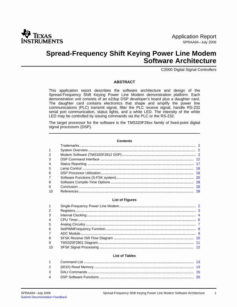
Application ReportSPRAA94–July 2006
Spread-Frequency Shift Keying Power Line ModemSoftware Architecture
.......................................................................................................... C2000 Digital Signal Controllers
ABSTRACT
This application report describes the software architecture and design of theSpread-Frequency Shift Keying Power Line Modem demonstration platform. Eachdemonstration unit consists of an eZdsp DSP developer’s board plus a daughter card.The daughter card contains electronics that shape and amplify the power linecommunications (PLC) transmit signal, filter the PLC receive signal, handle RS-232serial port communication, status lights, and a white LED. The intensity of the whiteLED may be controlled by issuing commands via the PLC or the RS-232.
The target processor for the software is the TMS320F28xx family of fixed-point digitalsignal processors (DSP).
ContentsTrademarks.......................................................................................... 2
1 System Overview ................................................................................... 22 Modem Software (TMS320F2812 DSP) ......................................................... 33 DSP Command Interface ........................................................................ 124 Status Reporting .................................................................................. 175 Lamp Control ...................................................................................... 186 DSP Processor Utilization........................................................................ 187 Software Functions (S-FSK system)............................................................ 208 Software Compile-Time Options ................................................................ 289 Conclusion ......................................................................................... 2810 References......................................................................................... 28
List of Figures
1 Single-Frequency Power Line Modem........................................................... 22 Registers............................................................................................. 33 Internal Clocking .................................................................................... 44 CPU Timer........................................................................................... 65 Analog Circuitry ..................................................................................... 76 SetPWMFrequency Function...................................................................... 87 ADC Module......................................................................................... 98 SFSK Receive ISR Flow Diagram .............................................................. 109 TMS320F2801 Diagram.......................................................................... 1110 SFSK Signal Processing ......................................................................... 12
List of Tables
1 Command List ..................................................................................... 132 (001h) Read Memory ............................................................................. 133 DALI Commands .................................................................................. 154 DSP Software Functions ......................................................................... 20
SPRAA94–July 2006 Spread-Frequency Shift Keying Power Line Modem Software Architecture 1Submit Documentation Feedback

www.ti.com
Trademarks
1 System Overview
1.1 PLC Timing Frequency
System Overview
5 Compile Flags ..................................................................................... 28
TMS320C2000 is a trademark of Texas Instruments.
The single-frequency power line modem is designed to demonstrate the use of spread-frequency shiftkeying in a power line modem to control a remote device. In the demonstration software, the remotedevice is a dimmable lamp fixture. The modem communicates with a host PC via an RS232 serialinterface.
Figure 1. Single-Frequency Power Line Modem
The spread frequency shift key (S-FSK) system uses a multiplier to detect received data. The S-FSKsystem uses a sample rate of 51/53ths of the carrier frequency Fm (Mark frequency).
Frequency in kHz Time in usec clock ticks @ 100 MIPS
Space Transmit Carrier 74.0 13.513 1351Frequency
Mark Transmit Carrier 63.3 15.797 1579Frequency
Receive Sample Rate 60.9 16.420 1642
Bit time 1.2 833.3 8333
Byte time 0.15 6666.4 66664
Spread-Frequency Shift Keying Power Line Modem Software Architecture2 SPRAA94–July 2006Submit Documentation Feedback

www.ti.com
1.2 Message Composition
PreambleBit Sync field
Subframeslot indicatorWord Sync
field message dataPause
End-of-Packet
16 bits 16 bits 38 bytes @ 8 bits/byte =304 bits 24 bits
message data format : P_sdu = M_pdu
Byte number: 0 1 2 3 4 … 30 37
Byte contents: FIFrame Indicator
Message word format
bit number 15 14 13 12 11 10 9 8 7 6 5 4 3 2 1 0
description b2 b2 b2 b2 b2 b2 b2 b2 b1 b1 b1 b1 b1 b1 b1 b1
2 Modem Software (TMS320F2812 DSP)
2.1 System Initialization
Modem Software (TMS320F2812 DSP)
Figure 2. Registers
Bit Sync Field 0xAAAA = 1010 1010 1010 1010
Word Sync Field 0x54C7 = 0101 0100 1100 0111
Pause Field xxxx xxxx xxxx xxxx xxxx xxxx
data xxxx xxxx
Total packet size = 16 + 16 + 38*8 + 24 = 360 bits
Total packet time = 360 bit / 1200 = 300 msec (assuming a 1200 baud rate)
Before entering the main loop, the main() function initializes the hardware and software.
1. Disable interrupts to clear all interrupt flag registers.2. Initialize system control registers, PLL, WatchDog, and clocks to default state.3. Set each GPIO pin to operate as either general-purpose I/O or to perform a specific dedicated function.4. Initialize the peripheral interrupt expansion (PIE) control registers and the interrupt service routine
table.5. If executing from FLASH, copy certain program functions from FLASH to RAM for faster execution.6. Configure all peripherals:
– External interface– CPU Timers - Generate period interrupts– Serial Communications Interface (SCI)– Analog-to-Digital Converters (ADC)
SPRAA94–July 2006 Spread-Frequency Shift Keying Power Line Modem Software Architecture 3Submit Documentation Feedback
www.ti.com
2.2 Time Base
2.2.1 CPU Clock
2.2.2 Peripheral Clock
Modem Software (TMS320F2812 DSP)
– Event Manager Timers - Controls period of PWM transmit waveform and receiver ADCsampling rate
7. Initialize variables
– Global variables– CRC table– UART message arrays– Diagnostic trace buffer– Lamp control variables
8. Read the device address from the jumpers.9. Arm the ADC to start converting input signals when triggered by the event manager.10. Enable interrupts.11. Enter the MainLoop( ) function, which does not return.
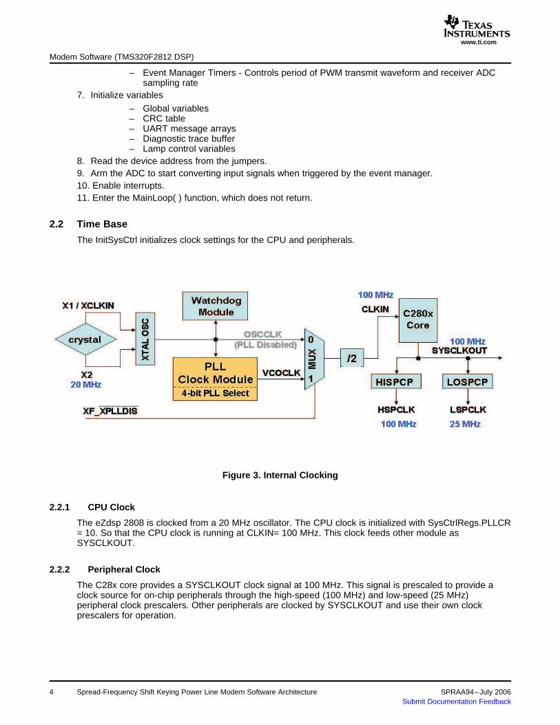
The InitSysCtrl initializes clock settings for the CPU and peripherals.
Figure 3. Internal Clocking
The eZdsp 2808 is clocked from a 20 MHz oscillator. The CPU clock is initialized with SysCtrlRegs.PLLCR= 10. So that the CPU clock is running at CLKIN= 100 MHz. This clock feeds other module asSYSCLKOUT.
The C28x core provides a SYSCLKOUT clock signal at 100 MHz. This signal is prescaled to provide aclock source for on-chip peripherals through the high-speed (100 MHz) and low-speed (25 MHz)peripheral clock prescalers. Other peripherals are clocked by SYSCLKOUT and use their own clockprescalers for operation.
Spread-Frequency Shift Keying Power Line Modem Software Architecture4 SPRAA94–July 2006Submit Documentation Feedback
www.ti.com
2.3 Main Loop
2.4 Interrupts
2.4.1 Periodic Interrupts
Modem Software (TMS320F2812 DSP)
The MainLoop function is run once per ADC interrupt. In each pass through the loop one of the functionslisted in the table below is performed according to the task_switch_counter state variable. Eachfunction in the MainLoop is intended to perform its function (or a part of it) quickly and then exit. A statevariable or some other flag is set for functions which require more processing than is reasonable in asingle pass through the loop, so that processing continues where it left off.
Function Name Operation
HandleUART( ) Handle incoming/outgoing serial data.
TaskCommand( ) Handle active commands.
ControlLamp( ) Adjust lamp intensity setting.
GenerateFloodPLCMessage( ) If the PLC bus has been idle long enough, this function builds a message packet thatcan be used to load the PLC bus with traffic. Useful for system debug, but should beturned off in a field-deployed system.
Then some functions are executed for every MainLoop pass through:
Function Name Operation
FillTxBuffer( ): Pending transmit messages, whether they are real or fake, are formattedand copied from the TXUserDataArray to the TxDataArray
ProcessRxPlcMsg( ) Recently completed receive message packets are processed to look forerrors and passed to the command handler if necessary.
Once the necessary functions have been executed, the processor is dropped into a low-power mode. Theidle mode will be exit once an interrupt wakes it up.
ISRTimer0( ) Implements the main system periodic timer. Occurs twice per1000 Hz control period.
ADCINT_ISR ( ) Handle incoming samples from the A/D converter. Runs at 60.9kHz for the S-FSK system.
T1PINT_ISR Runs once per transmit period of 63.3kHz.
Interrupts are allocated through the peripheral expansion as shown in TMS320x280x System Control andInterrupts Reference Guide (SPRU712). Both the ADC and the CPU Timer 0 interrupt are multiplexed inthe PIE Group 1 vectors. These interrupts are enabled in the interrupt table by:
PIE 1.6 ADC Interrrupt• PieCtrlRegs.PIEIER1.bit.INTx6 = 1;
PIE 1.7 CPU Timer0• PieCtrlRegs.PIEIER1.bit.INTx7 = 1;Interrupt
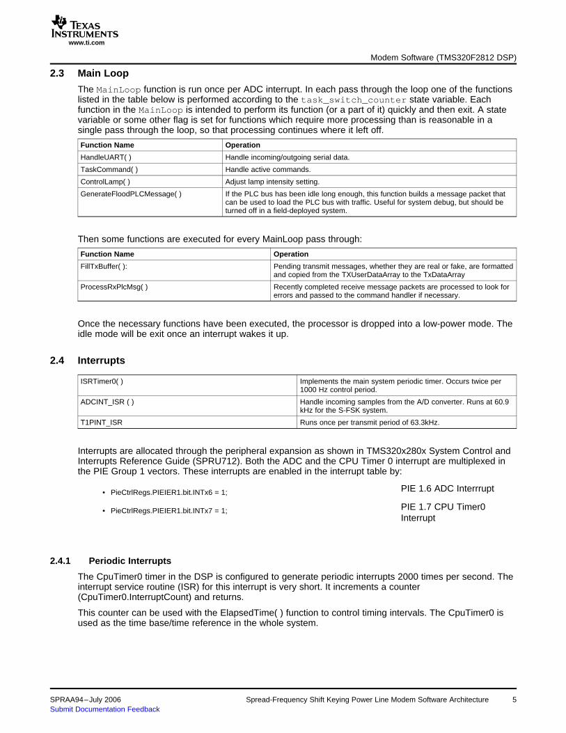
The CpuTimer0 timer in the DSP is configured to generate periodic interrupts 2000 times per second. Theinterrupt service routine (ISR) for this interrupt is very short. It increments a counter(CpuTimer0.InterruptCount) and returns.
This counter can be used with the ElapsedTime( ) function to control timing intervals. The CpuTimer0 isused as the time base/time reference in the whole system.
SPRAA94–July 2006 Spread-Frequency Shift Keying Power Line Modem Software Architecture 5Submit Documentation Feedback
www.ti.com
incrementCPU Timer 0
return
CPU Timer 0 Periodicinterrupt (2000/sec)
2.4.2 Transmit PWM and Timer Configuration
2.4.2.1 Event Manager
2.4.2.2 PWM Output
Modem Software (TMS320F2812 DSP)
Figure 4. CPU Timer
The Event Manager Timer 1 interrupt is processed every XXXXX.
Receive and transmit operation are periodically checked inPieVectTable.EPWM1_INT = &T1PINT_ISR
PWM frequency is derived from SYSCLKOUT = 100 MHz.
TBCLK = SYSCLKOUT / (HSPCLKDIV * CLKDIV)
EPwmxRegs.TBCTL.bit.HSPCLKDIV = 1
EPwmxRegs.TBCTL.bit.HSPCLKDIV CLKDIV = 1
Here TBCLK = 100 MHz.
The PLC transmitter uses one hardware event manager in the TMS3230C28xx to generate a transmitclock running in continuous up/down counting mode. The transmit clock value depends on the bit totransfer:
• Space frequency 74 kHz (2.5 MHz / 33.783)• Mark frequency 63.3 kHz (2.5 MHz/39.494)
The PWM period registers (TBPRD) are setup so that they run at the space/mark transmit frequency.
Space frequency setting Mark frequency setting
EPwm1Regs.TBPRD = TX_TPR_s; EPwm1Regs.TBPRD = TX_TPR_m;
EPwm2Regs.TBPRD = TX_TPR_s; EPwm2Regs.TBPRD = TX_TPR_m;
Spread-Frequency Shift Keying Power Line Modem Software Architecture6 SPRAA94–July 2006Submit Documentation Feedback
www.ti.com
0 0.5 1 1.5 2 2.5 3
time in
PWM1
PWM2
PWM1+PWM2 Line Driver
Modem Software (TMS320F2812 DSP)
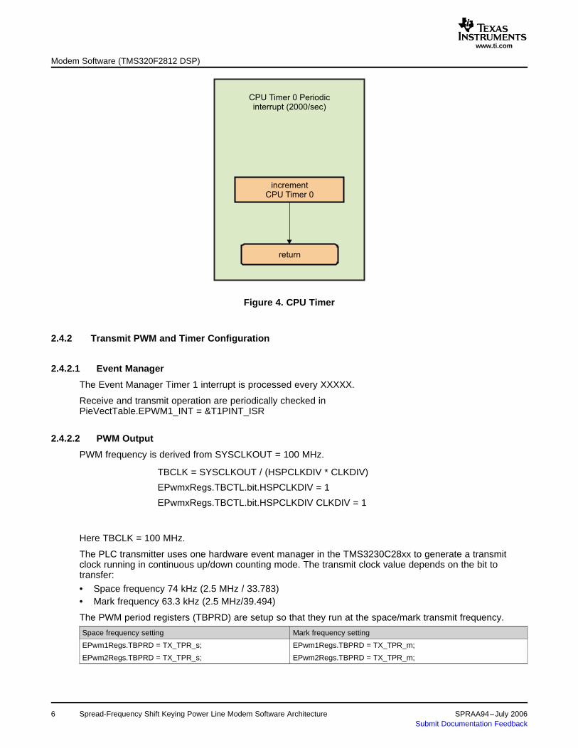
This clock is fed to two full-compare units. One compare unit is set to generate an output with 33.3% dutycycle, the other is set for 66.6% duty cycle:
Space frequency setting Mark frequency setting
EPwm1Regs.TBPRD = TX_TPR_s/3 EPwm1Regs.CMPA = TX_TPR_m/3;
EPwm2Regs.TBPRD = TX_TPR_s*2/3; EPwm2Regs.CMPA = TX_TPR_m*2/3;
The outputs of the two compare units are summed together by the analog circuitry on the power line driveramplifier. By adding these two signals together and then filtering the sum at the transmit line driver, amark or space sine wave carrier signal is produced.
Figure 5. Analog Circuitry
To modulate the signal, the carrier frequency of the signal is set once per bit time by modifying thecompare action control register ACTRA in SetPWMFrequency function. In this manner the clock remainsaligned throughout the transmit cycle with no discontinuities. The frequency modulation can be performedas a separate interrupt minor timing variations in the frequency modulation will have little effect on thetransmitted signal quality.
SPRAA94–July 2006 Spread-Frequency Shift Keying Power Line Modem Software Architecture 7Submit Documentation Feedback
www.ti.com
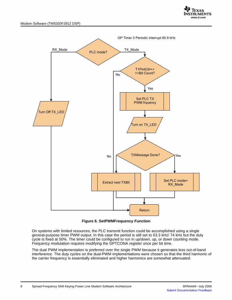
PLC mode?
T1PintCtrl++>=Bit Count?
TX_Mode
Set PLC TXPWM frquency
Turn on TX_LED
TXMessage Done?
Extract next TXBitSet PLC mode=
RX_Mode
YesNo
Turn Off TX_LED
Return
No
Yes
RX_Mode
GP Timer 3 Periodic interrupt 60.9 kHz
Modem Software (TMS320F2812 DSP)
Figure 6. SetPWMFrequency Function
On systems with limited resources, the PLC transmit function could be accomplished using a singlegeneral-purpose timer PWM output. In this case the period is still set to 63.3 kHz/ 74 kHz but the dutycycle is fixed at 50%. The timer could be configured to run in up/down, up, or down counting mode.Frequency modulation requires modifying the GPTCONA register once per bit time.
The dual PWM implementation is preferred over the single PWM because it generates less out-of-bandinterference. The duty cycles on the dual-PWM implementations were chosen so that the third harmonic ofthe carrier frequency is essentially eliminated and higher harmonics are somewhat attenuated.
Spread-Frequency Shift Keying Power Line Modem Software Architecture8 SPRAA94–July 2006Submit Documentation Feedback

www.ti.com
2.4.3 Receiver
2.4.3.1 Receive SFSK System Timing
ACQ_PSbits
CPS bitADCCLK (8.35<12.5)
To ADCpipline
samplingwindow
0111b
ADCTRL1
1b
( )1
sampling window ACQPS PS 1ADCCLK
æ ö÷ç ÷= + ´ç ÷ç ÷çè ø
ADCCLKPSbits
ADCTRL3
011b
( )FCLK
ADCCLKCPS 1
=+( )
HSPCLKFCLK
2 ADCCLKPS=
´
FCLK(16.7 MHz)
HSPCLK(100MHz)
2.4.3.2 Receiver Signal Processing
Modem Software (TMS320F2812 DSP)
The receive function samples the transmitted signal at a sample rate that is far below the Nyquistminimum sampling rate of 2x the carrier frequency. This under sampling technique generates intermediatefrequency that is used to detect the transmitted message data. It is critical that the receive clock period bevery consistent during the entire time that a message packet is being received.
The ADC module has several prescaler stages to generate any desired ADC operating clock speed. Thefollowing diagram defines the clock selection stages that feed the ADC module from the high speedperipheral clock running at 100 MHz.
Figure 7. ADC Module
The conversion rate of the ADC is set at 8.35 MHz.
The conversion is triggered by the ePWM3 module which generates a Fsamp = 60.9 kHz frequency. Astart of conversion (SOC) pulse is generated to the ADC to initiate a conversion sequence.
The ADC samples the filtered signal at a fixed frequency of Fsamp = 60.9 kHz which is:• 0.9621 the mark frequency and• 0.823 times the space frequency
So that 51 receive samples will be collected for each 53-cycle of a mark transmit bit time or 62-cycle of amark transmit bit time. This "down samples" the signal to a 1.2kHz waveform since these 51 samples willlook like two periods of a 1.2 kHz sine wave.
These 51 samples are fed into a 25 tap FIR filter to estimate the transmitted data bits.
The ADC interrupt is triggered by the completion of the A/D conversion process. The interrupt is handledby the ADCINT_ISR( ) function. This ISR function reads the most recent ADC values and then calls thedata detection routines. The routine to collect the ADC readings is called SmoothADCResults( ).Itcombines the results from A/D Converter, scale them, and convert them to signed values. After a receivesample is returned from, ArmAllSensors( ) is called to re-arm the A/D converters to await triggering forthe next sample time.
SPRAA94–July 2006 Spread-Frequency Shift Keying Power Line Modem Software Architecture 9Submit Documentation Feedback
www.ti.com
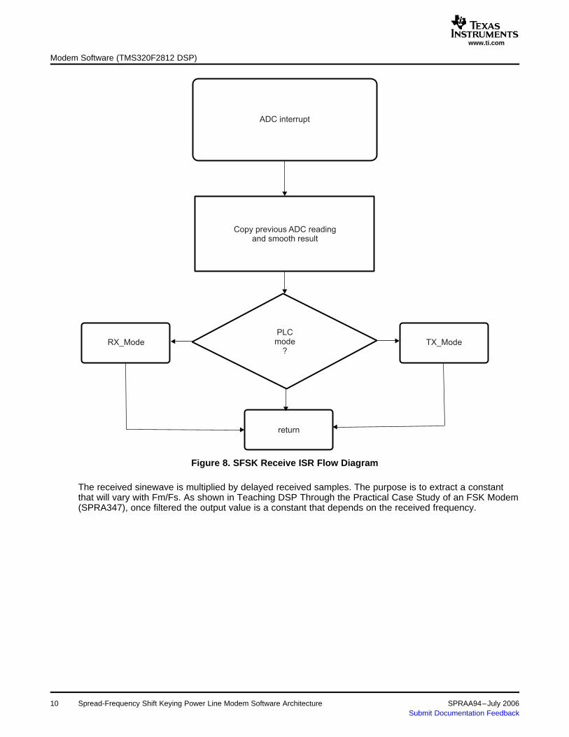
ADC interrupt
Copy previous ADC readingand smooth result
PLCmode
?TX_Mode
return
RX_Mode
Modem Software (TMS320F2812 DSP)
Figure 8. SFSK Receive ISR Flow Diagram
The received sinewave is multiplied by delayed received samples. The purpose is to extract a constantthat will vary with Fm/Fs. As shown in Teaching DSP Through the Practical Case Study of an FSK Modem(SPRA347), once filtered the output value is a constant that depends on the received frequency.
10 Spread-Frequency Shift Keying Power Line Modem Software Architecture SPRAA94–July 2006Submit Documentation Feedback

www.ti.com
0 1 Band PassFilter
Receivedsample multipli FIR
Data detection after ??
Delay
0 1
Receive sampled delayed
TMS320F2801
2.4.3.3 Synchronization
Modem Software (TMS320F2812 DSP)
Figure 9. TMS320F2801 Diagram
Once the receiver timing is properly synchronized to the transmitter, this step would only need to beperformed once per bit time, every 51 samples. Until the timing is synchronized, this step must beperformed more frequently. In the demonstration software it is run every sample time to aid in diagnosticsand debugging.
Later activity depends on which portion of the packet is being received. Once demodulated, a softwarelogic is utilized to detect received data structure as described in 1.2 Message composition paragraph. TheuRxMode is used to identify the packet field to be processed.
In every state, as soon as a bit transition is detected ( from 0 to 1 or from 1 to 0), the bitPhase counter isreset. As long as there is no new transition, it is incremented. If it reaches half a bit duration(BIT_DET_THRS) the bit value (detBit) is reputed stable/valid so that it is concatenated to the receiveddata (detData). Having the bitPhase counter exceeding the bit duration shows that there are twoconsecutive bits with the same polarity: the bitPhase is reset.
During the FIND_BITSYNC portion, the demodulator output is examined to detect the reception of thepacket preamble: 0xAAAA (BITSYNC_PATTERN). This 16-bit binary sequence corresponds to a polaritytransition for each bit. The detData vector is compared with BITSYNC_PATTERN. When equal, theuRxMode state is switch to FIND_WORDSYNC. During the FIND_WORDSYNC portion, the recentlyreceived data is compared to the known word sync pattern WORDSYNC_PATTERN (0x54C7). Thesample number in which a valid pattern match is first seen is recorded. When the valid pattern match is nolonger seen, the sample number is also recorded. The center of the bit timing window is then set to bemidway between the two recorded sample numbers. In case the WORDSYNC_PATTERN is not found theuRxMode state resumes to FIND_BITSYNC.
During the FIND_DATA portion, the received signal at the center of the bit timing window is stored in therxUserDataArray buffer. The rxDataArray value is parsed into data bytes, parity bits, and start/stop bits.The data bytes are then stored in the rxUserDataArray buffer.
During this time, the End-of-Pattern (EOP) field is sought amongst the data using the HammingDistance( )function. When the EOP pattern is seen, or when the maximum allowed message length has beenexceeded, the message is complete and the software switches back to FIND_BITSYNC mode.
The completed message is then checked for errors using the CRC and the parity bits. Valid messageswhose target address matches the receiver’s address are parsed and stored in the upCommand bufferwhich will later be interpreted by the TaskCommand( ) function in the MainLoop( ).
SPRAA94–July 2006 Spread-Frequency Shift Keying Power Line Modem Software Architecture 11Submit Documentation Feedback

www.ti.com
3 DSP Command Interface
3.1 Introduction
DSP Command Interface
Figure 10. SFSK Signal Processing
Commands to various devices on the PLC bus can be using the Graphical User Interface on a host PC,which then sends the command to the PLC modem board via an RS-232 serial interface. The DSPtranslates the RS-232 message into the proper format and sends it over the PLC bus.
The RS-232 serial port operates at 115.2 kbps, with 8 data bits, 1 stop bit, and no parity.
The basic flow of a command is as follows. The host (the PC) initiates a command by sending 32 words(64 bytes) of serial data that constitute a command (described below). The DSP (TMS320F2808) runningon the demonstration platform receives and interprets the serial data, executes the command, and sendsback a one word return code (2 bytes), followed by any requested data (all returned data in 16-bit wordformat also).
The following commands are available to configure and monitor the system, as well as exercise most of itsfunctions.
Spread-Frequency Shift Keying Power Line Modem Software Architecture12 SPRAA94–July 2006Submit Documentation Feedback

www.ti.com
3.2 (0002h) Write Memory
DSP Command Interface
Table 1. Command List
0001h Read Memory
0002h Write Memory
0003h Read Status
000Ah Direct Lamp Control
000Bh Lamp Control
000Ch Send PLC Message
000Dh Configure PLC Bus Flooder
000Fh Get local PLC Address
0020h Set Echo Acknowledge Address
0021h Echo Request
0022h Echo Acknowledge
Table 2. (001h) Read Memory
Parm # Description
0 Command number = 0001h
1 Control flags
bit 15 bit 14 bit 13 bit 12 bit 11 bit 10 bit 9 bit 8
bit 7 bit 6 bit 5 bit 4 bit 3 bit 2 bit 1 bit 0
MODE
2 Count
3-31 Address specification list
The Read Memory command is used to view the internal DSP data memory.
Parm 1, the flags register, controls how to read memory.
MODE 0 = Addresses specified in Parms 3-311 = Block read. Read starting at address in Parm3
Parm 2, the count value specifies the number of DSP memory addresses to be read. Since the DSP is a16-bit machine, the count specified refers to 16-bit words (not bytes).
If MODE = 0, Count determines the number of words to be read (<= 29), and the desired addresses to beread should be listed in Parms 3 through 31.
If MODE = 1, A block read will be performed beginning at the address specified in Parm3, ‘Count’ wordswill be read.
Parm # Description
0 Command number = 0002h
1 Control flags
bit 15 bit 14 bit 13 bit 12 bit 11 bit 10 bit 9 bit 8
bit 7 bit 6 bit 5 bit 4 bit 3 bit 2 bit 1 bit 0
MODE
2 Count
3-31 These parms are split into two word pairs:Low word: AddressHigh word: Data
SPRAA94–July 2006 Spread-Frequency Shift Keying Power Line Modem Software Architecture 13Submit Documentation Feedback
www.ti.com
3.3 (0003h) Read Status
3.4 (000Ah) Direct Lamp Control
DSP Command Interface
The Write Memory command is used to modify the internal DSP data memory.
MODE 0 = Addresses mode1 = Block read. Read starting at address in Parm3
In Address mode, up to fourteen words may be written per command (exact number specified by Count).The parameters 3-31 are paired into address/data sets.
In Block Fill mode, an entire address range can be set to the same value (e.g., 0000, FFFF, DEAD,…).Parm3 specifies the starting address to be written to, Parm4 specifies the 16-bit data word to be written,and Count specifies the number of addresses to write. Any size block is allowed (be careful).
Parm# Description
0 Command number = 0003h
1 Reset flag
This command is used by the GUI program to request status from the modem. The status consists ofcounters used to measure the bit error rate.
Reset flag 1: Reset (fill with zero) the contents of the status arrays ulPlcStats and ulBerStats.
else: Place the contents of the ulPlcStats and ulBerStats arrays on the Rs-232 UART FIFO for read by thePC.
The format of data returned is :
byte# Description
0 return code
1 count
2-N ulPlcStats
N-M ulBerStats
Parm# Description
0 Command number = 000Ah
1 Lamp intensity setting
This command directly sets the lamp intensity setpoint level. The lamp intensity will fade to the newsetpoint level at a rate determined by the Fade Time variable. If the commanded setting is between zeroand the lamp minimum level, the intensity will stop at the minimum level. If the commanded setting isbetween 254 and the lamp maximum level, the intensity will stop at the maximum level. If the commandedsetting is 0, the lamp will fade to the minimum level, then turn off.
If this command is issued through the RS-232 port, the device attached to the RS-232 will respond,regardless of its address. If this command was passed inside a PLC packet, only the device with thematching address will respond.
Spread-Frequency Shift Keying Power Line Modem Software Architecture14 SPRAA94–July 2006Submit Documentation Feedback

www.ti.com
3.5 (000Bh) Lamp Control
DSP Command Interface
Parm# Description
0 Command number = 000Bh
1 DALI command number
This command controls the lamp using one of the special DALI commands. The commands can be usedto set the intensity to a previously memorized setting, adjust fade rate and fade time, memorize settings,or adjust the light intensity.
If this command is issued through the RS-232 port, the device attached to the RS-232 will respond,regardless of its address. If this command was passed inside a PLC packet, only the device with thematching address will respond.
Table 3. DALI Commands
DALI Cmd # Command Name Description
0 OFF Turn lamp off instantly.
1 UP Fade up for 200 ms if already lit, at rate determined byFade Rate.
2 DOWN Fade down for 200 ms if already lit at rate determined byFade Rate. Do not turn off.
3 STEP_UP Step up one step if already lit.
4 STEP_DOWN Step down one step if already lit.
5 RECALL_MAX_LEVEL Set intensity to MaxLevel, without fading.
6 RECALL_MIN_LEVEL Set intensity to MinLevel, without fading.
7 STEP_DOWN_AND_OFF Step down one step. Turn off if already at MinLevel.
8 ON_AND_STEP_UP Step up one step. If lamp was off, ignite it first.
9-15 --RESERVED–
16-31 GO_TO_SCENE x, {x=0..15} Fade to new scene level. If lamp was off, ignite it first.
32 RESET
33 STORE_ACTUAL_LEVEL_IN_THE_DTR
34-41 --RESERVED–
42 STORE_THE_DTR_AS_MAX_LEVEL
43 STORE_THE_DTR_AS_MIN_LEVEL
44 STORE_THE_DTR_AS_SYSTEM_FAILURE_LEVEL
45 STORE_THE_DTR_AS_POWER_ON_LEVEL
46 STORE_THE_DTR_AS_FADE_TIME
47 STORE_THE_DTR_AS_FADE_RATE
48-63 --RESERVED–
64-79 STORE_THE_DTR_AS_SCENE x, {x=0..15}
80-95 REMOVE_FROM_SCENEx, {x=0..15}
96-111 ADD_TO_GROUP g, {g = 0..15}
112-127 REMOVE_FROM_GROUP g, {g = 0..15}
128-255 Additional DALI Commands Not implemented in demo unit.
SPRAA94–July 2006 Spread-Frequency Shift Keying Power Line Modem Software Architecture 15Submit Documentation Feedback
www.ti.com
3.6 (000Ch) Send PLC Message
3.7 (000Dh) Configure PLC Bus Flooder
3.8 (0020h) Set Echo Acknowledge Address
3.9 (0021h) Echo Request
DSP Command Interface
Parm # Description
0 Command number = 000Ch
1 Target address Hi
2 Target address Lo
3 Embedded command number
4 Parameter 0
This command is used to initiate a PLC Bus message to another node. Only the node whose addressmatches will respond.
The embedded command number can be any valid command. Generally, it will be 0x0A: Direct lampcontrol or 0x0B: lamp control.
Parm # Description
0 Command number = 000Dh
1 Flood rate: packets per Second
The Configure PLC Bus Flooder command is used to control the rate at which fake PLC packets aregenerated to flood with PC bus with traffic. This is useful for exercising the bus under high-trafficconditions and for testing transmission error rates. It would rarely be used in a field-deployed installation.
Parm # Description
0 Command number = 0020h
1 Control flags
bit 15-8 bit 7-2 bit 1 bit 0
BER BERRead Reset
2 Slave Address
3 Flood rate (1 to 15 Hz)
This command defines the address to send an echo command to. Each packet transmitted at the "floodrate" contains an echo request command which is addressed to the modem defined using this command.
Parm # Description
0 Command number = 0021h
1 Sender's address, high byte
2 Sender's address, low byte
3 Ack command (0022h)
When sending this command, set the address (bytes 0 and 1 of the transmit buffer) to the addressspecified by the set echo acknowledge address command, followed by the above command format.Increment the echo sent element in the BerStats counter array.
When receiving this command, send an echo acknowledge (0022h) command on the power line,addressed to the sender. Increment the echo request element in the BerStats counter array.
16 Spread-Frequency Shift Keying Power Line Modem Software Architecture SPRAA94–July 2006Submit Documentation Feedback

www.ti.com
3.10 (0022h) Echo Acknowledge
4 Status Reporting
4.1 PLC Statistics
4.1.1 DPSK Statistics Array Assignments
4.1.2 PSK Statistics Array Assignments
Status Reporting
Parm # Description
0 Command number = 0022h
1 Sender's address, high byte
2 Sender's address, low byte
3 Status of original Echo command reception
When sending this command, set the address (bytes 0 and 1 of the transmit buffer) to the addressspecified by the last Echo Request command received.
When receiving this command, Increment the Echo Ack element in the BerStats counter array.
The array ulPlcStats is used to store information about the performance of the PLC communicationchannel.
Name Description
TX_CNT Packets transmitted.
TX_COLLISION Invalid packets seen while transmitting.
RX_CNT Packets that started to be received.
RX_GOOD Packets received successfully.
RX_ERR_ZEROCROSS Packets that did not have a valid zero-crossing between the bitsync and word sync fields.
RX_ERR_WORDSYNC_TO Packets where a valid word sync pattern was not seen shortlyafter the zero crossing.
RX_ERR_WORDSYNC Packets where the word sync pattern was invalid.
RX_ERR_EOP Packets where the End-Of-Packet signal was not seen.
RX_ERR_CRC Data error detected by Cyclic Redundancy Code.
RX_ERR_PARITY Parity error detected in data field.
RX_ERR_PATTERN Content of flood message did not match known pattern.
RX_ERR_MSGLEN Message was invalid length.
Name Description
TX_CNT Count of packets transmitted.
TX_COLLISION Count of BitSync patterns seen while in transmit mode (Not usewhen modem enabled to receive its own transmit signal.)
RX_CNT Count of packets received before CRC is checked.
RX_GOOD Count of packets received with good CRC.
RX_PREDET_COUNT Count of BitSync patterns recognized
RX_SYNCDET_COUNT Count of WordSync patterns recognized
RX_EOP_COUNT Count of End-of-Packet (EOP) patterns recognized
SPRAA94–July 2006 Spread-Frequency Shift Keying Power Line Modem Software Architecture 17Submit Documentation Feedback

www.ti.com
4.1.3 Status LED Definitions
5 Lamp Control
6 DSP Processor Utilization
6.1 F2808 Hardware Utilization
Lamp Control
RX_ERR_WORDSYNC_TO Count of events timed out looking for WordSync
RX_EOP_TIMEOUT Count of events timed out looking for the EOP pattern
RX_MSGLEN_ERROR Count of events where more bytes were received than can fit inthe receive buffer.
RX_ERR_CRC Count of packets where the CRC sent does not match the CRCcalculated from the received data
RX_ERR_PARITY Count of words where the sent parity does not match the paritycalculated from the received data.
The PLC daughter board contains three PLC status LEDs.
Label Color IO PORT Description
RX_GOOD Green GPIOA8 The latest PLC packet wasreceived successfully.
RX_BUSY Yellow GPIOA9 A PLC packet is beingreceived.
TX Red GPIOA10 A PLC packet is beingtransmitted.
The demonstration platform uses a white LED to simulate the function of a fluorescent lamp ballast. Thelamp is controlled by commands to the CmdLamp( ) function. The commands closely resemble those usedin the DALI lighting control standard.
The intensity setpoint and fade rate are set using commands received by the CmdLamp( ) function. Thecommand fade rate is used to calculate the interval between fading steps. The elapsed time since the lastfading step is monitored in the MainLoop( ) function, and when a new fading step is due, theControlLamp( ) function is called. The lamp intensity setting is moved toward the target lamp setpoint ata rate determined by the Fade Rate and/or Fade Time. The ControlLamp( ) function then calls theSetLampInsensity( ) function.
The SetLampIntensity( ) function translates the intensity setpoint level, which ranges from 0 to 254,into a lamp voltage between 0% and 100%. The voltage levels are logarithmically spaced, ranging from aminimum of 0.1% at setting level 1 to 100% at setting level 254. Setting level 0 yields zero output voltage.The duty cycle of the 15-bit PWM DAC hardware is then programmed to generate the proper voltage level.For fluorescent lamps that utilize a fixed duty cycle and adjust the lamp current by frequency control, thePWM DAC period register could be changed instead of the duty cycle register.
Some lamps may be unable to operate properly at very low voltage settings. For these lamps, the DALIstandard allows a programmable minimum intensity level. The CmdLamp( ) and ControlLamp( )functions ensure that intensity settings between zero and the minimum are handled properly.
The DALI standard includes provisions for igniting fluorescent lamps. The demonstration platform softwareincludes stub functions to handle the ignition delays.
USED IN REAL APPLICATION
Function Registers Pins
PLC Tx Waveform
Tx+ output EPwm1Regs.CMPA PWM1
18 Spread-Frequency Shift Keying Power Line Modem Software Architecture SPRAA94–July 2006Submit Documentation Feedback

www.ti.com
6.2 Memory Usage (SFSK System)
6.2.1 Memory Configuration
6.2.2 RAM Reduction
DSP Processor Utilization
Tx- output EPwm2Regs.CMPA PWM3
Period register EPwm1Regs.TBPRDEPwm2Regs.TBPRD
Tx Bias Enable GpioDataRegs.GPADAT.bit.GPIO13 GPIOA13
ADC Rx Input
ADC Input ADCIN6 ADCINA6
Period register EPwm3Regs.TBPRD
USED ONLY FOR DEMO BOARD
Function Registers Pins
LED Intensity
PWM output EPwm6Regs.CMPA PWM6
Period register EPwm6Regs.TBPRD
RS-232 Interface
Serial Data Tx SCITXDA
Serial Data Rx SCIRXDA
RTS GPIOF0
CTS GPIOF1
Status LEDs
Rx Good GPIOA8
Rx Busy GPIOA9
Tx GPIOA10
Option Jumpers
Opt1 GPIOB9
Opt0 GPIOB10
Opt2 GPIOB11
Opt3 GPIOB12
SaveTrace Enabled, SLOW_BETWEEN_MSGS=True, CORR_LEN=FIR_LEN,TRACE_BUFF_LEN=0x1000
name origin length used usage
Page 0: PRAMH0 003FA000 00002000 00013B7 Program
PRAMM0 000000002 000003FE 0000275
Page 1:
DRAMM1 00000400 00000400 00000200 Stack
ECAN_AMBOX 00006100 00000200 00000100 CRC table
DRAML0 003F8000 00001000 000003AE General variables
DRAML1 003F9000 00001000 000005C2 Trace Buffer
CSM_PWL 003F7FF8 00000008 00000008
The demo code was developed using an eZdsp card with a TM320F2808 processor. Consideration hasbeen given to reducing the memory usage to enable use of a lower-cost DSP in the TMS320F280x family.By reducing or eliminating the Trace Buffer, the F2806 becomes a viable option.
SPRAA94–July 2006 Spread-Frequency Shift Keying Power Line Modem Software Architecture 19Submit Documentation Feedback

www.ti.com
6.3 Processor MIPS Utilization
6.4 FLASH Memory
7 Software Functions (S-FSK system)
7.1 Function Names and Descriptions
Software Functions (S-FSK system)
TMS320F2801 TMS320F2806 TMS320F2808
Frequency (MHz) 100 100 100
RAM (Words) 6K 10K 18K
Flash (Words) 16K 32K 64K
OTP ROM (Words) 1K 1K 1K
Boot Loader Available YES YES YES
PWM Channels 8 16 16
12-bit A/D (#Channels) 16 16 16
Timers 3/3/3 6/6/3 6/6/3
If most of the program was moved to FLASH memory, it might be possible to squeeze the application intoan F2801. The wait states in the FLASH would make the processor too slow to run all the code fromFLASH, but about 800 words of time-critical code could be run from RAM at full speed.
Other ideas for shrinking RAM requirements:
• The 256-word CRC table is generated during DSP initialization by the InitCRCtable( ) function andremains constant thereafter. This could be computed at compile time and stored in FLASH.
• The 256-word Intensity table in command.c is constant and could be moved to FLASH.• The UART functions are required for the bus master, but would be unneeded in a slave device like
ballast. Eliminating the UART functions and their variables would save about 400 words of datamemory and 250 words of program memory.
• The 1k stack is far larger than needed; 128 words would probably be sufficient.• With all of these changes and only the time-critical code running from RAM, the RAM requirement
could be brought below 4k for the program + data variables.• The program could eliminate about 0.5k of demo-only code, but would probably need to add about
0.5k more to the command handler. About 1k of the PLC code would be common with the ballastcontrol / PFC code.
Items in gray are for demo purpose and could be removed from a real PLC system.
Table 4. DSP Software Functions
Function Name R Description
main.c
InitSysCtrl( ); Y Select GPIO for the device or for the specific application PLLsetup: SYSCLKOUT = 100 MIPS
InitGpio( ); Initialize pie control registers to default state and populate thePIE vector table with pointers to the shell interrupt serviceroutines (ISR) functions found in DSP28_DefaultIsr.c
InitPieCtrl(); Initialize PIE control registers
InitPieVectTable( ); Populate the PIE vector table with default pointers
20 Spread-Frequency Shift Keying Power Line Modem Software Architecture SPRAA94–July 2006Submit Documentation Feedback

www.ti.com
Software Functions (S-FSK system)
Table 4. DSP Software Functions (continued)
BootCopy Y Copies the InitFlash function from FLASH into RAM so that itcan adjust the wait states of the flash. (Do not try to adjustFlash wait states while running from flash) Only used whenFLASH is used.
InitFlash( ); Y Set up flash wait states (This function must reside in RAM)
InitCpuTimers( ); Y PRD=FFFFFFFF and TPR = 0Timer = SYSCLKOUT/((PRD+1) * (TPR+1)
InitSci( );
ConfigureADCs( ); Y CLKPS=6 – CPS = 1, CLK=HSPCLK/12=8.35 MHz
ConfigureGPTimers( ); Y Sets up GP timers for the PWM and ADC
InitializeGlobals( ); Y Global variable initialization.
InitializeUARTArray( ); Clear out array of data to be sent to UART.
ConfigCpuTimer Y This function initializes the selected timer to the periodspecified by the "Freq" and "Period" parameters. The "Freq"is entered as "MHz" and the period in "uSeconds". The timeris held in the stopped state after configuration.
ArmAllSensors( ); Y Arm the sensors for the next reading
ElapsedTime Returns elapsed time between two events.
GenerateFakePLCMessage Generate a fake message for the PLC to send.This function is required only for development and testing.
ISRTimer0 Y This timer is used to implement the main system periodictimer.
MainLoop Y Infinite loop to execute tasks.
Main Y Performs setup functions, then enters infinite loop to executetasks.
command.c
CmdConfigFlooder N This function sets the flood rate at which fake PLC messagesare generated.
CmdLamp N This function implements the commands that control thelamp intensity and fade rate. The commands used are verysimilar to the DALI lighting control standard.
CmdPLCCommand N This function allows a host connected to this board viaRS-232 to issue commands over the PLC bus.
CmdReadMemory N Reads memory in the DSP and sends value to DSP viaUART.
CmdWriteMemory N Modify the DSP memory based on commands received fromUART.
ControlLamp N This function adjusts the intensity of the lamp, moving ittoward its setpoint at the proper fade rate.
InitLampVars N This function initializes the lamp command variables to theirreset values.
SetLampIntensity N Set the lamp PWM DAC to set the lamp intensity.
TaskCommand N This task actually executes commands and responds to theMCU. This task gets posted after an MCU interrupt specifyinga command occurs. This function reads the parmsacknowledges the command, then executes the commandand responds to the MCU when complete.While primarily intended for commands received from theUART, commands may also be received from the PLC.
Transmit_new.c
adc_isr Y This ISR services the A/D converter's conversion completeinterrupt.The most recently measured samples are filtered and theA/D is armed to be triggered by an Event Manager timerevent.
SPRAA94–July 2006 Spread-Frequency Shift Keying Power Line Modem Software Architecture 21Submit Documentation Feedback
www.ti.com
Software Functions (S-FSK system)
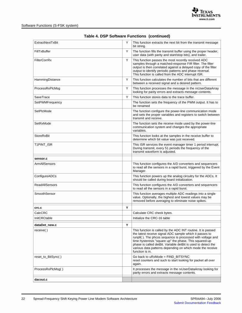
Table 4. DSP Software Functions (continued)
ExtractNextTxBit Y This function extracts the next bit from the transmit messagebit string.
FillTxBuffer Y The function fills the transmit buffer using the proper header,user data (with parity and start/stop bits), and trailer.
FilterCorrRx Y This function passes the most recently received ADCsamples through a matched-response FIR filter. The filteroutput is then correlated against a delayed copy of the filteroutput to identify periodic patterns and phase reversal.This function is called from the ADC interrupt ISR.
HammingDistance Y This function calculates the number of bits that are differentbetween a received signal and a desired pattern.
ProcessRxPlcMsg Y This function processes the message in the rxUserDataArraylooking for parity errors and extracts message contents.
SaveTrace Y This function stores data to the trace buffer.
SetPWMFrequency The function sets the frequency of the PWM output. It has tobe renamed
SetPlcMode The function configure the power-line communication modeand sets the proper variables and registers to switch betweentransmit and receive.
SetRxMode The function sets the receive mode used by the power-linecommunication system and changes the appropriatevariables.
StoreRxBit This function looks at the samples in the receive buffer todetermine which bit value was just received.
T1PINT_ISR This ISR services the event manager timer 1 period interrupt.During transmit, every 51 periods the frequency of thetransmit waveform is adjusted.
sensor.c
ArmAllSensors This function configures the A/D converters and sequencersto read all the sensors in a rapid burst, triggered by the EventManager.
ConfigureADCs This function powers up the analog circuitry for the ADCs. Itshould be called during board initialization.
ReadAllSensors This function configures the A/D converters and sequencersto read all the sensors in a rapid burst.
SmoothSensor This function averages multiple ADC readings into a singlevalue. Optionally, the highest and lowest values may beremoved before averaging to eliminate noise spikes.
crc.c Y
CalcCRC Calculate CRC check bytes.
InitCRCtable Initialize the CRC-16 table
dataDet_new.c Y
receive( ) This function is called by the ADC INT routine. It is passedthe latest receive signal ADC sample which it passes torunpll( ). The phcos sequence is processed with voltage andtime hysteresis "square up" the phase. This squared-upphase is called detBit. Variable detBit is used to detect thevarious data patterns depending on which mode the receivefunction is in.
reset_to_BitSync( ) Go back to uRxMode = FIND_BITSYNCreset counters and such to start looking for packet all overagain.
ProcessRxPlcMsg( ) It processes the message in the rxUserDataArray looking forparity errors and extracts message contents.
dacout.c
Spread-Frequency Shift Keying Power Line Modem Software Architecture22 SPRAA94–July 2006Submit Documentation Feedback

www.ti.com
Software Functions (S-FSK system)
Table 4. DSP Software Functions (continued)
WritePWMDAC Sends a requested value to the PWM DACs. Used to controllamp voltage.
diag.c
CmdDiagTraceConfig This function is used to configure the Trace buffer.
InitDiagTrace Initialize the diagnostic trace buffer to begin tracingimmediately and stop when the trace buffer is full. Initializingthe trace buffer in this manner is useful for bring up.
RunTrace Spew diagnostics if appropriate. – NOT USED –
gpio.c
InitGpio Initializes the GPIO registers. The function determines whichIO pins should be used for their predefined peripheral output,and which are to be GPIO.
sci.c
InitSci Initialize the SCI ports to a known state.
timer.c
ConfigureDog This function disables the WatchDog timer and sets itsprescale ratio.
ConfigureGPTimers This function configures the GP timer periods.
DelayNms This function delays N milliseconds. It locks out interrupts for1 us at a time, so use cautiously in time-critical routines.
DelayNus This function delays N microseconds. It locks out interruptsfor 1 us at a time, so use cautiously in time-critical routines.
FeedDog This function resets the WatchDog timer.
SleepDog This function disables the WatchDog timer.
WakeDog This function enables the WatchDog timer.
uart.c
HandleUART This function is used to send/receive data to the UART. It iscalled once each servo period. Because the definedcommand interface only allows one command to be issued ata time, the flow of UART data consists of a command comingin to the DSP, and then a response going out. A secondcommand can not be sent until the reply from the first isreceived. If there is data to be sent, do worry about incomingdata. Additionally, if we make it into this routine with nothingto go out, since we do not have multiple prioritized tasks tointerrupt us, we will not have to worry about sending anythingfor the rest of the time (we can just sit and wait to see if thereis anything to read.
InitializeUARTArray This function is used to initialize the UART, so that it comesup with nothing in the buffer to send out.
WriteUART This function is used to interface between the code and thetask which sends data to the UART (TaskWriteUART). Thisroutine accepts a count and a pointer to the start of data. Itthen inserts an entry into the array UARTDataOut whichTaskWriteUART uses to send out data. Note that it will storethe count and pointer, not buffer the actual data, so thecalling function must keep the variable around (static orglobal), or else use the function WriteUARTValue( ).
WriteUARTValue This function is used to send a single value to the UART. Thecalling function doesn't have to worry about memorymanagement. This function takes the passed value, assignsit to a variable, then sends a pointer to that variable alongwith the destination FPGA address and a count of one, to theWriteUART() function. The "variable" used, is an element in acircular buffer. The buffer is the same length as theUARTDataOut array, so this should not ever have valuesoverwritten (we should get an error from WriteUART() first).
SPRAA94–July 2006 Spread-Frequency Shift Keying Power Line Modem Software Architecture 23Submit Documentation Feedback

www.ti.com
Software Functions (S-FSK system)
Table 4. DSP Software Functions (continued)
vardefs.c
InitializeGlobals Assign initialization values to global variables.This function gets called from main( ) as part of the setupprocess.
DSP28_CpuTimers.c
ConfigCpuTimer This function initializes the selected timer to the periodspecified by the "Freq" and "Period" parameters. The "Freq"is entered as "MHz" and the period in "uSeconds". The timeris held in the stopped state after configuration.
InitCpuTimers This function initializes CPU timer0 to a known state.
DSP28_PieCtrl.c
InitPieCtrl This function initializes the Peripheral Interrupt Expansioncontrol registers to a known state.
DSP28_PieVect.c
InitPieVectTable This function initializes the PIE vector table to a known state.This function must be executed after boot time.
DSP28_SysCtrl.c
InitFlash This function initializes the Flash Control registersThis function MUST be executed out of RAM. Executing it outof OTP/Flash will yield unpredictable results
InitSysCtrl This function initializes the System Control registers to aknown state.
DSP28_Xintf.c
InitXintf This function initializes the External Interface to a knownstate.
DSP28_DefaultIsr.c This file contains default interrupt service routines for everyinterrupt. Most of them are unused. Unless noted otherwisebelow, the default ISR is merely a stub function that branchesto itself and hangs the processor.
CAPINT1_ISR
CAPINT2_ISR
CAPINT3_ISR
CAPINT4_ISR
CAPINT5_ISR
CAPINT6_ISR
CMP1INT_ISR
CMP2INT_ISR
CMP3INT_ISR
CMP4INT_ISR
CMP5INT_ISR
CMP6INT_ISR
DATALOG_ISR
ECAN0INTA_ISR
ECAN1INTA_ISR
EMUINT_ISR
ILLEGAL_ISR
INT13_ISR
INT14_ISR
MRINTA_ISR
24 Spread-Frequency Shift Keying Power Line Modem Software Architecture SPRAA94–July 2006Submit Documentation Feedback

www.ti.com
Software Functions (S-FSK system)
Table 4. DSP Software Functions (continued)
MXINTA_ISR
NMI_ISR
PDPINTA_ISR
PDPINTB_ISR
PIE_RESERVED
RTOSINT_ISR
SCIRXINTA_ISR
SCIRXINTB_ISR
SPIRXINTA_ISR
SPITXINTA_ISR
T1CINT_ISR
T1OFINT_ISR
T1UFINT_ISR
T2CINT_ISR
T2OFINT_ISR
T2PINT_ISR
T2UFINT_ISR
T2CINT_ISR
T2OFINT_ISR
T3PINT_ISR
T3UFINT_ISR
T4CINT_ISR
T4OFINT_ISR
T4PINT_ISR
T4UFINT_ISR
TINT0_ISR
USER0_ISR
USER10_ISR
USER11_ISR
USER1_ISR
USER2_ISR
USER3_ISR
USER4_ISR
USER5_ISR
USER6_ISR
USER7_ISR
USER8_ISR
USER9_ISR
WAKEINT_ISR
XINT1_ISR
XINT2_ISR
rsvd_ISR
SPRAA94–July 2006 Spread-Frequency Shift Keying Power Line Modem Software Architecture 25Submit Documentation Feedback

www.ti.com
7.2 Function Call Hierarchy - main( )Software Functions (S-FSK system)
Level Function
1 main
2 InitSysCtrl
2 InitGpio
2 InitPieCtrl
2 InitPieVectTable
2 BootCopy
2 InitFlash
2 InitCRCtable
2 InitXintf
2 InitCpuTimers
2 InitSci
2 ConfigureADCs
3 DelayNus
2 ConfigureGPTimers
3 SleepDog
3 FeedDog
2 InitializeGlobals
2 InitalizeUARTArray
2 InitDiagTrace
2 InitLampVars
2 ConfigCpuTimer
2 ArmAllSensors
2 MainLoop
3 ElapsedTime
3 GenerateFakePLCMessage
3 FillTxBuffer
4 CalcCRC
4 SetPlcMode
5 SetPWMFrequency
5 ExtractNextTxBit
5 ArmAllSensors
3 ProcessRxPlcMsg
4 CalcCRC
3 TaskCommand
4 CmdReadMemory
5 WriteUARTValue
6 WriteUART
4 CmdWriteMemory
5 WriteUARTValue
6 WriteUART
4 CmdLamp
5 InitLampVars
5 WriteUARTValue
6 WriteUART
4 CmdLamp
5 InitLampVars
26 Spread-Frequency Shift Keying Power Line Modem Software Architecture SPRAA94–July 2006Submit Documentation Feedback

www.ti.com
7.3 Function Call Hierarchy - ADCINT_ISR ( )
7.4 Function Call Hierarchy - T1PINT_ISR ( )
Software Functions (S-FSK system)
5 WriteUARTValue
6 WriteUART
4 CmdPLCCommand
5 WriteUARTValue
6 WriteUART
4 CmdConfigFlooder
5 WriteUARTValue
6 WriteUART
4 WriteUARTValue
5 WriteUART
3 ControlLamp
4 SetLampIntensity
3 HandleUART
4 InitSci
3 FeedDog
3 HandlePLC
4 SetPlcMode
5 SetPWMFrequency
5 ExtractNextTxBit
5 ArmAllSensors
4 ExtractNextTxBit
Level Function
1 ADCINT_ISR
2 FilterCorrRx
3 ArmAllSensors
3 SmoothADCResults
3 FIR2
3 AutoCorr
3 SetRxMode
3 StoreRxBit
3 HammingDistanceEOPEOP
3 SaveTrace
Level Function
1 T1PINT_ISR
2 SetPWMFrequency
2 SetPlcMode
3 SetPWMFrequency
3 ExtractNextTxBit
2 ExtractNextTxBit
SPRAA94–July 2006 Spread-Frequency Shift Keying Power Line Modem Software Architecture 27Submit Documentation Feedback

www.ti.com
8 Software Compile-Time Options
9 Conclusion
10 References
Software Compile-Time Options
The DSP software contains many compiler flags to allow for customization of the software to the intendedapplication.
Many important compile flags are listed in Table 5 below.
Table 5. Compile Flags
Compile Flag Default Value Description
TRACE_BUF_LEN 0x1000 Sets size of diagnostics buffer used bySaveTrace function. When set to 0, theSaveTrace function is not compiled tosave space and execution time.
MIPS 100 Sets MIPS rate for DSP. Valid values are150 and 120.
USE_CRC True Use Cyclic Redundancy Code to verifyvalidity of data.
XOR_TX_DATA True When true, pre-codes data so that thedifferential receiver outputs the correctdata with no additional processing.
XOR_RX_DATA ~True When true, accepts data that has not beendifferentially precoded and converts itto beread correctly. More susceptible to noisethan XOR_TX_DATA, but ensurescompatibility with generic Lonworkstransmitters.
SLOW_BETWEEN_MSGS True Reduces the MIPS load betweenmessages by only running the correlatorduring every 5th sample time.
FIR_LEN 25 Number of ADC samples in one PLC bittime.
CORR_LEN FIR_LEN Number of samples used for correlation.Valid values are 25 and 5. Using 5 is notrecommended because it degrades thedata error rate severely.
OVERSAMPLE_RATE 4 Sets the number of ADC readings that arecombined together to make onemeasurement. Valid values are 1 through16. Recommended values are 3,4,6, and10.
Tests in labs and environment where noise and perturbation are limited are good. However thedemodulation being based on autocorrelation it is not noise robust as any non-coherent method. In orderto deploy a such a demodulation model in the field it might be necessary to use coherent demodulationwhere the carrier frequency is recovered. This will require the system to observe the Nyquist criteria sothat sampling frequency will be at least twice the max of carriers. Once acquired the input samples will bepre-filtered to split isolate the carrier bands (around space and mark frequency). Then the energy on bothcarriers will be computed with an FFT algorithm. Since only 2 frequencies need to be measured instead ofthe full spectrum, it might be interesting to implement Goertzel functions which compute signal energy ona few pre-defined frequencies.
• TMS320C2000™ Digital Signal Controller Power Line Communication User’s Guide (SPRU714)• TMS320x280x DSP System Control and Interrupts Reference Guide (SPRU712)• Teaching DSP Through the Practical Case Study of an FSK Modem (SPRA347)
28 Spread-Frequency Shift Keying Power Line Modem Software Architecture SPRAA94–July 2006Submit Documentation Feedback

IMPORTANT NOTICE
Texas Instruments Incorporated and its subsidiaries (TI) reserve the right to make corrections, modifications,enhancements, improvements, and other changes to its products and services at any time and to discontinueany product or service without notice. Customers should obtain the latest relevant information before placingorders and should verify that such information is current and complete. All products are sold subject to TI’s termsand conditions of sale supplied at the time of order acknowledgment.
TI warrants performance of its hardware products to the specifications applicable at the time of sale inaccordance with TI’s standard warranty. Testing and other quality control techniques are used to the extent TIdeems necessary to support this warranty. Except where mandated by government requirements, testing of allparameters of each product is not necessarily performed.
TI assumes no liability for applications assistance or customer product design. Customers are responsible fortheir products and applications using TI components. To minimize the risks associated with customer productsand applications, customers should provide adequate design and operating safeguards.
TI does not warrant or represent that any license, either express or implied, is granted under any TI patent right,copyright, mask work right, or other TI intellectual property right relating to any combination, machine, or processin which TI products or services are used. Information published by TI regarding third-party products or servicesdoes not constitute a license from TI to use such products or services or a warranty or endorsement thereof.Use of such information may require a license from a third party under the patents or other intellectual propertyof the third party, or a license from TI under the patents or other intellectual property of TI.
Reproduction of information in TI data books or data sheets is permissible only if reproduction is withoutalteration and is accompanied by all associated warranties, conditions, limitations, and notices. Reproductionof this information with alteration is an unfair and deceptive business practice. TI is not responsible or liable forsuch altered documentation.
Resale of TI products or services with statements different from or beyond the parameters stated by TI for thatproduct or service voids all express and any implied warranties for the associated TI product or service andis an unfair and deceptive business practice. TI is not responsible or liable for any such statements.
Following are URLs where you can obtain information on other Texas Instruments products and applicationsolutions:
Products Applications
Amplifiers amplifier.ti.com Audio www.ti.com/audio
Data Converters dataconverter.ti.com Automotive www.ti.com/automotive
DSP dsp.ti.com Broadband www.ti.com/broadband
Interface interface.ti.com Digital Control www.ti.com/digitalcontrol
Logic logic.ti.com Military www.ti.com/military
Power Mgmt power.ti.com Optical Networking www.ti.com/opticalnetwork
Microcontrollers microcontroller.ti.com Security www.ti.com/security
Low Power Wireless www.ti.com/lpw Telephony www.ti.com/telephony
Video & Imaging www.ti.com/video
Wireless www.ti.com/wireless
Mailing Address: Texas Instruments
Post Office Box 655303 Dallas, Texas 75265
Copyright 2006, Texas Instruments Incorporated