Embed Size (px)
Citation preview
Enterprise
SSD Form Factor
Version 1.0
SSD Form Factor Version1_0.docx
December 20, 2011
Copyright 2011, SSD Form Factor Working Group
Please send comments to:
Enterprise SSD Form Factor 1.0
2
Copyright © 2012 SSD Form Factor Work Group, All rights reserved.
INTELLECTUAL PROPERTY DISCLAIMER
THIS SPECIFICATION IS PROVIDED “AS IS” WITH NO WARRANTIES WHATSOEVER INCLUDING ANY
WARRANTY OF MERCHANTABILITY, FITNESS FOR ANY PARTICULAR PURPOSE, OR ANY WARRANTY
OTHERWISE ARISING OUT OF ANY PROPOSAL, SPECIFICATION, OR SAMPLE.
NO LICENSE, EXPRESS OR IMPLIED, BY ESTOPPEL OR OTHERWISE, TO ANY INTELLECTUAL PROPERTY
RIGHTS IS GRANTED OR INTENDED HEREBY.
THE SSD FORM FACTOR WORK GROUP DISCLAIMS ALL LIABILITY, INCLUDING LIABILITY FOR
INFRINGEMENT OF PROPRIETARY RIGHTS, RELATING TO IMPLEMENTATION OF INFORMATION IN
THIS SPECIFICATION. THE SSD FORM FACTOR WORK GROUP DOES NOT WARRANT OR REPRESENT
THAT SUCH IMPLEMENTATION(S) WILL NOT INFRINGE SUCH RIGHTS.

Enterprise SSD Form Factor 1.0
3
1 OVERVIEW ................................................................................................................... 6
1.1 Overview ......................................................................................................................................... 6 1.2 Goals .............................................................................................................................................. 6 1.3 Technical Summary ........................................................................................................................ 6
1.3.1 Flexible Drive Backplane option ............................................................................................................. 7 1.4 Scope .............................................................................................................................................. 8 1.5 Outside of Scope ............................................................................................................................ 9
2 SIGNAL LIST .............................................................................................................. 10
2.1 Signal Lists ................................................................................................................................... 10 2.2 Connector pin out ......................................................................................................................... 12 2.3 PRSNT# - Presence Detect and IfDet# - Interface Detect Signal Definition ................................ 14 2.4 DualPortEn# - PCIe Dual Port Enable .......................................................................................... 14 2.5 Reserved(WAKE#/OBFF#), Reserved(ClkReq#/DevSLP#)......................................................... 15 2.6 ePERst[1:0]# - PCIe Reset ........................................................................................................... 15
3 CONNECTOR MECHANICAL ............................................................................................ 16
3.1 Connector Mechanical Drawing notes .......................................................................................... 17 3.2 Connector Plug Mechanical Drawings.......................................................................................... 17 3.3 Connector Plug Mechanical Drawings - Details ........................................................................... 19 3.4 Connector Receptacle Mechanical Drawings ............................................................................... 21 3.5 Connector Intermateability Mechanical Drawings ........................................................................ 22 3.6 Recommended Board Layouts (informative) ................................................................................ 23 3.7 Characteristics shared with other Specifications (informative) ..................................................... 25 3.8 Cable Retention Mechanical Drawings ......................................................................................... 26
4 HOT PLUG AND REMOVAL ............................................................................................. 31
4.1 Limit current inrush ....................................................................................................................... 32 4.2 Detecting Enterprise PCIe SSD Insertion/Removal ..................................................................... 33 4.3 PCIe Hardware and Reset System Requirements ....................................................................... 33 4.4 Software Implications of Hot Swap (Informative) ......................................................................... 35
5 DUAL PORT OPERATION ............................................................................................... 37
5.1 Dual Port Mode (implications of DualPortEn#) ............................................................................. 38
6 SM-BUS OPERATION ................................................................................................... 39
6.1 Simple Accesses to Vital Product Data (VPD) ............................................................................. 39 6.2 Extended SM-Bus management ................................................................................................... 39
7 ELECTRICAL (POINTER TO OTHER SPECIFICATIONS) .......................................................... 40
7.1 Electrical Channel ......................................................................................................................... 40 7.2 Presence and Interface Detect ..................................................................................................... 40 7.3 ePERst[1:0] ................................................................................................................................... 41 7.4 Power – 12V ................................................................................................................................. 41 7.5 Power 3.3Vaux ............................................................................................................................. 41
8 REFERENCES AND BIBLIOGRAPHY .................................................................................. 43
8.1 References ................................................................................................................................... 43 8.2 References Under Development .................................................................................................. 43 8.3 Formal Bibliography ...................................................................................................................... 43
9 SM-BUS - INFORMATIVE APPENDIX ................................................................................ 45
9.1 SM-Bus Vital Product Data (VPD) ................................................................................................ 45
Enterprise SSD Form Factor 1.0
4
9.2 SM-Bus Standard Capability definitions ....................................................................................... 46 9.3 SM-Bus MCTP commands ........................................................................................................... 46
10 SYSTEM USAGE – INFORMATIVE APPENDIX .................................................................. 47
10.1 Pin usage across standards ...................................................................................................... 47 10.2 System Usage Examples .......................................................................................................... 51 10.3 Connector Keying (Informative) ................................................................................................ 53
11 SPECIFICATION CONVENTIONS ................................................................................... 55
11.1 Definitions ................................................................................................................................. 55 11.1.1 PCI Express® (PCIe) ........................................................................................................................... 55 11.1.2 PCI Express® Generation 2 (PCIe Gen2) ............................................................................................ 55 11.1.3 PCI Express® Generation 3 (PCIe Gen3) ............................................................................................ 55 11.1.4 PCI Express® x4 (PCIe x4) .................................................................................................................. 55 11.1.5 SFF standards ...................................................................................................................................... 55 11.1.6 SSD ...................................................................................................................................................... 55
11.2 Keywords .................................................................................................................................. 55 11.2.1 mandatory ............................................................................................................................................ 55 11.2.2 may ...................................................................................................................................................... 55 11.2.3 optional ................................................................................................................................................. 55 11.2.4 R, RSVD ............................................................................................................................................... 55 11.2.5 reserved ............................................................................................................................................... 55 11.2.6 shall ...................................................................................................................................................... 56 11.2.7 should ................................................................................................................................................... 56

Enterprise SSD Form Factor 1.0
5
Table of Figures Figure 1: Example configurations ................................................................................................................................... 7 Figure 2: Flexible Backplane Implementation ................................................................................................................ 8 Figure 3: Signal List Summary (pin counts) ................................................................................................................. 10 Figure 4: Signal List Table (defining specification) ....................................................................................................... 11 Figure 5: Pin Out Drawing (Receptacle pin naming). ................................................................................................... 12 Figure 6: Drive type - Pin decoding .............................................................................................................................. 14 Figure 7: Connector Mechanical Overview .................................................................................................................. 16 Figure 8: Connector Examples ..................................................................................................................................... 16 Figure 9: Connector Plug Mechanical Drawing – Top View ......................................................................................... 17 Figure 10: Connector Plug Mechanical Drawing – Drive Insertion View ...................................................................... 17 Figure 11: Connector Plug Mechanical Drawing – Bottom View (outside of enclosure) ............................................... 18 Figure 12: Connector Plug Mechanical Drawing – End View (showing latch slot) ....................................................... 18 Figure 13: Connector Plug Mechanical Drawing – Detail A (key) ................................................................................. 19 Figure 14: Connector Plug Mechanical Drawing – Detail C (key pins) ......................................................................... 19 Figure 15: Connector Plug Mechanical Drawing – Detail B (Tongue) .......................................................................... 20 Figure 16: Connector Plug Mechanical Drawing – Section D-D (Tongue cross section).............................................. 20 Figure 17: Connector Plug Mechanical Drawing – Drive Keep-out Area ...................................................................... 21 Figure 18: Connector Receptacle Mechanical Drawing – Drive insertion view ............................................................ 21 Figure 19: Connector Receptacle Mechanical Drawing – Section E-E (Receptacle) ................................................... 22 Figure 20: Enterprise PCIe SSD Connector Datum -A- Centered in Receptacle ......................................................... 23 Figure 21: SFF-8482 Plug Datum -A- Biased Opposite Key in Receptacle slot ........................................................... 23 Figure 22: Right Angle Plug Board Layout - Drive (informative) ................................................................................... 24 Figure 23: Vertical Receptacle Board Layout - Backplane (informative) ...................................................................... 25 Figure 24: Cable Retention: Latch and Key Overview.................................................................................................. 27 Figure 25: Cable Retention Mechanical Drawing – Representative Cable Housing ..................................................... 28 Figure 26: Cable Release Clearance - Representative Cable Housing ........................................................................ 29 Figure 27: Representative Cable Housing with flat ribbon cables ................................................................................ 30 Figure 28: Hot Plug Current Inrush Limiting ................................................................................................................. 32 Figure 29: System Reset Timing .................................................................................................................................. 34 Figure 30: Reset Timing Details (PCI SIG CEM, 2007) ................................................................................................ 35 Figure 31: Single Port and Dual Port example ............................................................................................................. 37 Figure 32: Typical SSD Form Factor Channel ............................................................................................................. 40 Figure 33: Power (12V) specifications .......................................................................................................................... 41 Figure 34: Power 3.3VAux specifications ..................................................................................................................... 42 Figure 35: SM Bus Vital Product Data .......................................................................................................................... 45 Figure 36: SM Bus Capability Definition ....................................................................................................................... 46 Figure 37: Pin usage across Existing standards .......................................................................................................... 49 Figure 38: Pin usage across Emerging standards........................................................................................................ 50 Figure 39: Backplane for Enterprise SSD (PCIe x4), SATA & SATA Express (Client PCIe) ........................................ 51 Figure 40: Backplane for Enterprise SSD (PCIe x4), SAS & SATA.............................................................................. 52 Figure 41: Backplane for SAS X4, SAS & SATA .......................................................................................................... 52 Figure 42 Cross Standard Connector Keying ............................................................................................................... 54
Enterprise SSD Form Factor 1.0
6
1 Overview
1.1 Overview
This specification defines the electrical and mechanical requirements for a PCI Express connection to the existing standard 2.5” and 3.5” disk drive form factors. This is intended for PCIe connections to SSDs (Solid State Drives) for the enterprise market of servers and storage systems. This provides a new PCIe form factor that is storage friendly, leveraging both the existing PCIe specification and the existing 2.5” and 3.5” drive mechanical specifications. This standard allows system designs that can support a flexible mix of new enterprise PCI Express drives, and existing SAS and SATA drives.
Note: The References and Bibliography are listed at the end, in section 8 on page 43. The Specification Conventions are listed at the end, in section 11 on page 55. This includes the standard material such as the definition of “Shall”, “Should”, “May”, etc. and bibliographic material to reference specifications. Also included are definitions of terms such as “PCIe”, “PCIe Gen 3”, “PCIe x4”, “SFF”, and “SSD”.
1.2 Goals
The following are the characteristics of the product envisioned using this specification:
PCIe1 connection to Enterprise Solid State Drives (SSDs).
Standardize connector and form factor – but enabling innovation using the PCIe model.
Fits in existing drive mechanical enclosures using a disk backplane. Supports both 2.5” drive mechanical enclosures and 3.5” drive mechanical enclosures.
Support customer expectation for storage device: o Externally accessible & Hot Swappable (with surprise removal) o Support existing OEM’s existing drive infrastructure (device detection and indicators) o Support existing OEM thermal architectures, and support for future enhancements.
Support for both single port (typical servers), or dual port (typically storage systems).
Meet projected system storage device performance requirements for systems introduced in the 2H 2011 to 2016 timeframe.
Enables flexible system designs that support Enterprise PCIe Express SSDs and SAS or SATA drives using the same connector family, allow systems to support flexible mix of capacity (SAS or SATA hard drives) or Enterprise PCIe SSDs.
1.3 Technical Summary
A technical summary of the “SSD Form Factor Working Group” is:
Focus is on connector which is supported in both the existing 2.5” and 3.5” form factors.
Supports the 2.5” drive (SFF-8223, 2007) specification2 unchanged, or supports the 3.5” drive
(SFF-8301, 1999) specification unchanged.
Compatible with existing SAS connector (SFF-8482, 2006). Meaning the connectors allow interoperation, see Section 10. For example a new backplane receptacle would accept new or existing drives. The connector is doubled sided extension to existing SAS connector. New pins are 0.8mm pitch across the complete B-side and on top of SAS key.
Support for PCIe x4 (Gen2 and Gen3) signaling. References PCIe specifications for high speed electrical specifications – unchanged.
The electrical channel is assumed to be similar to SAS3 channel – short board trace, longer cable, trace on storage backplane, SSD.
1 Definition of PCIe and reference specification are included in section 8 on page 40
2 Definition of SAS, SATA, SFF and reference specifications including official designations (EIA, ANSI,
INCITIS numbers) are included in section 8 on page 40

Enterprise SSD Form Factor 1.0
7
25W connector limit, with 12V only delivery. Expecting Enterprise PCIe SSDs at range of power levels, and expecting Enterprise PCIe SSDs to support software settable power limit, and temperature monitoring.
There is optional support for 3.3V aux to allow probing device information before system power on (Vital Product Data – VPD – over SM bus.)
Pins list is the merging of SATA/SAS signals and the PCIe x4 plus PCIe side band. The actual high speed lanes for SAS and SATA are separate pins from the Enterprise PCIe pins. This enables direct connection to SAS or SATA controller and separate pins to high performance Enterprise PCIe upstream device without an intervening repeater, mux, or controller.
Support Single x4 or Dual x2 port as (2@x2) with dual PCIe side band
Supports Hot swap support details, basics same as SAS
Supports SM bus for out of band discovery
Supports PCIe power management features
Figure 1 shows example configurations.
Figure 1: Example configurations
1.3.1 Flexible Drive Backplane option
The current technical direction allows for system implementations that support flexible storage backplane bays supporting a mix of Enterprise PCIe or SAS or SATA or SATA Express devices. The system would provide both a PCIe connection along with a separate connection to a SAS or SATA controller. The system support infrastructure would also have to be extended to support the super-set capabilities (power amperage, management signaling).
Disk Bay Backplane
2.5” SSD Form Factor
Device
(Enterprise PCIe SSD)
PCIe upstream
(e.g. CPU x4 PCIe port)
Conn
ecto
r
PCIe x4
Typical Server configuration
conn
µC
Disk Backplane
2.5” SSD Form Factor
Device (Enterprise PCIe SSD)
Controller
A
Conn
ecto
r
PCIe x2
Typical Storage configuration
Controller
B
PCIe x2
conn
conn
Enterprise SSD Form Factor 1.0
8
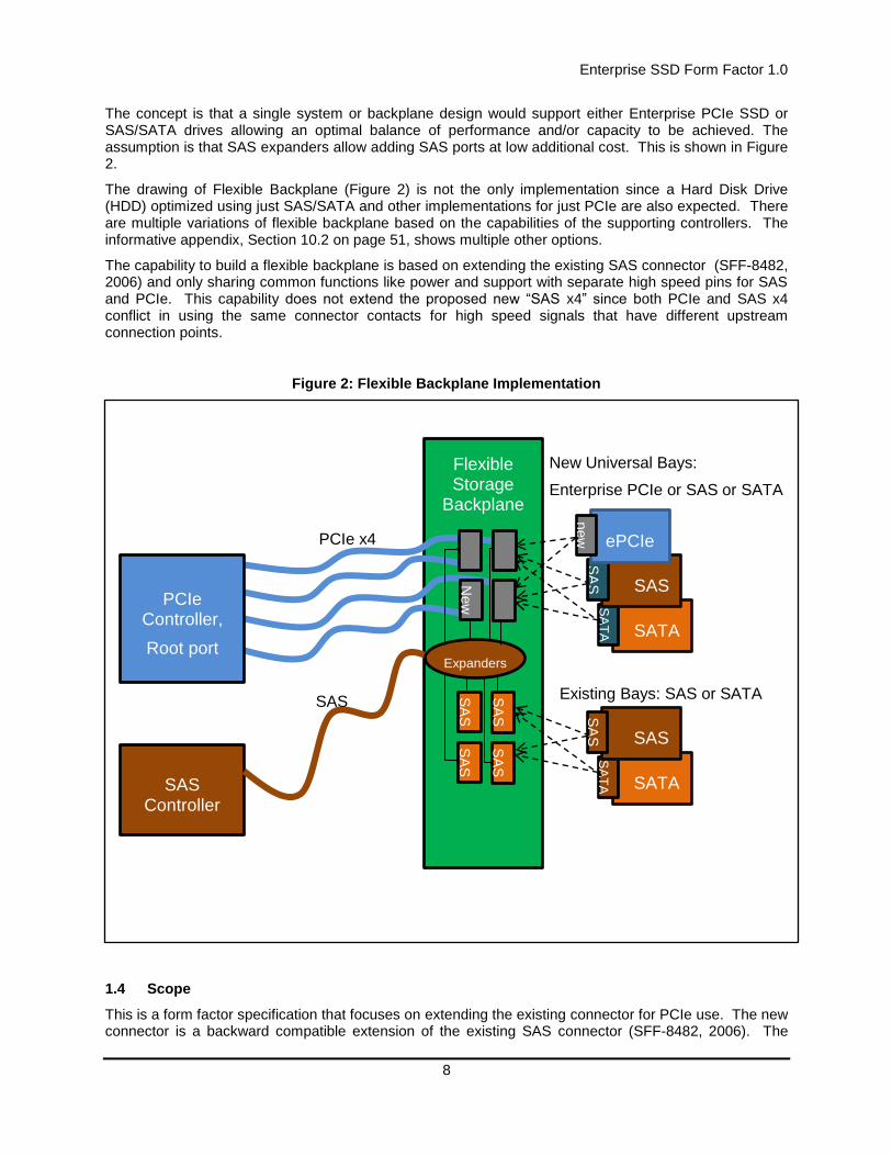
The concept is that a single system or backplane design would support either Enterprise PCIe SSD or SAS/SATA drives allowing an optimal balance of performance and/or capacity to be achieved. The assumption is that SAS expanders allow adding SAS ports at low additional cost. This is shown in Figure 2.
The drawing of Flexible Backplane (Figure 2) is not the only implementation since a Hard Disk Drive (HDD) optimized using just SAS/SATA and other implementations for just PCIe are also expected. There are multiple variations of flexible backplane based on the capabilities of the supporting controllers. The informative appendix, Section 10.2 on page 51, shows multiple other options.
The capability to build a flexible backplane is based on extending the existing SAS connector (SFF-8482, 2006) and only sharing common functions like power and support with separate high speed pins for SAS and PCIe. This capability does not extend the proposed new “SAS x4” since both PCIe and SAS x4 conflict in using the same connector contacts for high speed signals that have different upstream connection points.
Figure 2: Flexible Backplane Implementation
1.4 Scope
This is a form factor specification that focuses on extending the existing connector for PCIe use. The new connector is a backward compatible extension of the existing SAS connector (SFF-8482, 2006). The
Flexible Storage
Backplane
SATA
SA
TA
PCIe x4
SAS
SA
S
ePCIe
new
SAS Controller
SATA
SA
TA
SAS
SA
S
Expanders
SA
S
SA
S
SA
S
SA
S
N
ew
SAS Existing Bays: SAS or SATA
New Universal Bays:
Enterprise PCIe or SAS or SATA
PCIe Controller,
Root port

Enterprise SSD Form Factor 1.0
9
overall mechanical form factor is compliant with the 2.5” form factor (SFF-8223, 2007) or 3.5” form factor (SFF-8301, 1999).
This specification defines the following:
Pin list and pin out of the new connector.
Mechanical definition of the new connector, including latching, keying, and retention.
Limited electrical specification (largely reference PCIe CEM and SAS Specifications).
Hardware hooks for Hot Swap
Signal definitions for Dual Port
Definitions of a basic product data accessible from SM-Bus
1.5 Outside of Scope
This specification is only normative for connector and related definitions (just listed)
The actual usage is not defined. While we envisioned having an SSD using NVM Express interface (formerly. eNVMHCI), that is not required and other PCIe devices would work.
The specification does give possible usage (aka. implementation notes) for Hot Swap, Dual Port, and SM-bus but the details are system implementation specific. These are just meant to illustrate a possible usage.
Specifically this specification is informative (not normative) in the following areas:
The drive outline is defined by EIAECA-720 (SFF-8223, 2007) for 2.5” drives or by EIA-740 (SFF-8301, 1999) for 3.5” drives. The drive carrier and storage enclosure are implementation specific.
Mechanical drawings normative document will be SFF-8639 (SFF-8639, Draft 2011) when it is approved. Until that document is approved, this specification is normative.
SAS signal definitions and specifications – normative are the SAS Specifications (T10, Various). Note: SAS-x4 signal definitions in this specification are a proposal to T10.
PCIe signal definitions and specifications – normative are the PCIe Specifications (PCI SIG, various).
SATA/SATA Express signal definitions and specification – normative are the SATA Specifications (SATA-IO, various).
Note: SATA Express signal definitions in this specification are a proposal to the SATA-IO Cabcon
SM Bus signal definitions and specifications – normative are the SM Bus specifications (SMBus, 2000)
PCIe device functionality and register details and the SM-bus registers are defined by the specific device specifications. Likely referencing the PCIe Specification for standard PCIe device discovery and setup.
Specific system implementation of presence pins (hot plug)
Specific system implementation of dual port functionality
References to other related connectors - specifically keying and overlaying of pins.
This is envisioned as a PCIe SSD specification and there is no standardization for additional connections beyond the drive PCIe connector. There are both backplane and cable versions of the connector receptacle.
Enterprise SSD Form Factor 1.0
10
2 Signal List
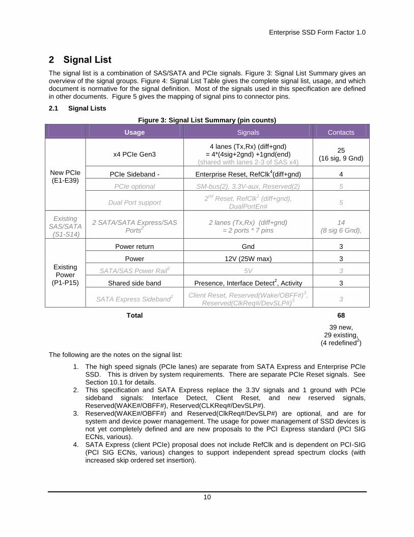
The signal list is a combination of SAS/SATA and PCIe signals. Figure 3: Signal List Summary gives an overview of the signal groups. Figure 4: Signal List Table gives the complete signal list, usage, and which document is normative for the signal definition. Most of the signals used in this specification are defined in other documents. Figure 5 gives the mapping of signal pins to connector pins.
2.1 Signal Lists
Figure 3: Signal List Summary (pin counts)
Usage Signals Contacts
New PCIe (E1-E39)
x4 PCIe Gen3 4 lanes (Tx,Rx) (diff+gnd)
= 4*(4sig+2gnd) +1gnd(end) (shared with lanes 2-3 of SAS x4)
25 (16 sig, 9 Gnd)
PCIe Sideband - Enterprise Reset, RefClk4(diff+gnd) 4
PCIe optional SM-bus(2), 3.3V-aux, Reserved(2) 5
Dual Port support 2
nd Reset, RefClk
1 (diff+gnd),
DualPortEn# 5
Existing SAS/SATA (S1-S14)
2 SATA/SATA Express/SAS Ports
2 2 lanes (Tx,Rx) (diff+gnd)
= 2 ports * 7 pins 14
(8 sig 6 Gnd),
Existing Power
(P1-P15)
Power return Gnd 3
Power 12V (25W max) 3 SATA/SAS Power Rail
2 5V 3
Shared side band Presence, Interface Detect2, Activity 3
SATA Express Sideband2
Client Reset, Reserved(Wake/OBFF#)3,
Reserved(ClkReq#/DevSLP#)3
3
Total 68
39 new, 29 existing,
(4 redefined2)
The following are the notes on the signal list:
1. The high speed signals (PCIe lanes) are separate from SATA Express and Enterprise PCIe SSD. This is driven by system requirements. There are separate PCIe Reset signals. See Section 10.1 for details.
2. This specification and SATA Express replace the 3.3V signals and 1 ground with PCIe sideband signals: Interface Detect, Client Reset, and new reserved signals, Reserved(WAKE#/OBFF#), Reserved(CLKReq#/DevSLP#).
3. Reserved(WAKE#/OBFF#) and Reserved(ClkReq#/DevSLP#) are optional, and are for system and device power management. The usage for power management of SSD devices is not yet completely defined and are new proposals to the PCI Express standard (PCI SIG ECNs, various).
4. SATA Express (client PCIe) proposal does not include RefClk and is dependent on PCI-SIG (PCI SIG ECNs, various) changes to support independent spread spectrum clocks (with increased skip ordered set insertion).
Enterprise SSD Form Factor 1.0
11
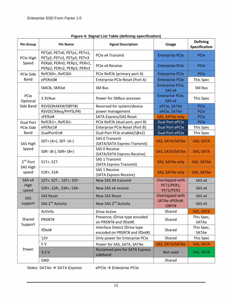
Figure 4: Signal List Table (defining specification)
Pin Group Pin Name Signal Description Usage Defining
Specification
PCIe High Speed
PETp0, PETn0, PETp1, PETn1, PETp2, PETn2, PETp3, PETn3
PCIe x4 Transmit Enterprise PCIe PCIe
PERp0, PERn0, PERp1, PERn1, PERp2, PERn2, PERp3, PERn3
PCIe x4 Receive Enterprise PCIe PCIe
PCIe Side Band
RefClk0+, RefClk0- PCIe RefClk (primary port A) Enterprise PCIe PCIe
ePERst0# Enterprise PCIe Reset (Port A) Enterprise PCIe This Spec
PCIe Optional
Side Band
SMClk, SMDat SM Bus Enterprise PCIe,
SAS x4 SM Bus
3.3VAux Power for SMbus accesses Enterprise PCIe,
SAS x4 This Spec
RSVD(WAKE#/OBFF#) Reserved for system/device power management
ePCIe, SATAe PCIe
RSVD(ClkReq/PHYSLP#) ePCIe, SATAe PCIe
sPERst# SATA Express/SAS Reset SAS, SATAe only PCIe
Dual Port PCIe Side
Band
RefClk1+, RefClk1- PCIe RefClk (dual port, port B) Dual Port ePCIe PCIe
ePERst1# Enterprise PCIe Reset (Port B) Dual Port ePCIe This Spec
DualPortEn# Dual Port PCIe enable(2@x2) Dual Port ePCIe This Spec
SAS High Speed
S0T+ (A+), S0T- (A-) SAS 0 Transmit (SATA/SATA Express Transmit)
SAS, SATA/SATAe SAS, SATA
S0R- (B-), S0R+ (B+) SAS 0 Receive (SATA/SATA Express Receive)
SAS, SATA/SATAe SAS, SATA
2nd Port SAS High
speed
S1T+, S1T- SAS 1 Transmit (SATA Express Transmit)
SAS, SATAe only SAS, SATAe
S1R+, S1R- SAS 1 Receive (SATA Express Receive)
SAS, SATAe only SAS, SATAe
SAS x4 High
speed
S2T+, S2T-, S3T+, S3T- New SAS X4 transmit Overlapped with PET1/PER1, PET2/PER2
SAS x4
S2R+, S2R-, S3R+, S3R- New SAS x4 receive SAS x4
SAS support
SAS Reset New SAS Reset Overlapped with SATAe sPERst#,
OBFF#
SAS x4
SAS 2nd Activity New SAS 2nd Activity SAS x4
Shared Support
Activity Drive Active Shared SAS, SATA
PRSNT# Presence; (Drive type encoded on PRSNT# and IfDet#)
Shared This Spec,
SATAe
IfDet# Interface Detect (Drive type encoded on PRSNT# and IfDet#)
Shared This Spec,
SATAe
Power
12V Only power for Enterprise PCIe Shared This Spec
5 V Power for SAS, SATA, SATAe SAS, SATA/SATAe SAS, SATA
3.3 V Reclaimed pins for SATA Express sideband
Not used SAS, SATA
GND Shared
Notes: SATAe SATA Express ePCIe Enterprise PCIe

Enterprise SSD Form Factor 1.0
12
2.2 Connector pin out
Figure 5: Pin Out Drawing (Receptacle pin naming).
Pin # Mating Name Signal Description Usage Drive
E7 3rd RefClk0+ ePCIe Primary RefClk + ePCIe input
E8 3rd RefClk0- ePCIe Primary RefClk - ePCIe input
E9 2nd GND Ground
E10 3rd PETp0 ePCIe 0 Transmit + ePCIe input
E11 3rd PETn0 ePCIe 0 Transmit - ePCIe input
E12 2nd GND Ground
E13 3rd PERn0 ePCIe 0 Receive - ePCIe output
E14 3rd PERp0 ePCIe 0 Receive + ePCIe output
E15 2nd GND Ground
E16 3rd RSVD Reserved
S8 2nd GND Ground
S9 3rd S1T+ SAS/SATAe 1 Transmit + SAS+SATAe input
S10 3rd S1T- SAS/SATAe 1 Transmit - SAS+SATAe input
S11 2nd GND Ground
S12 3rd S1R- SAS/SATAe 1 Receive - SAS+SATAe output
S13 3rd S1R+ SAS/SATAe 1 Receive + SAS+SATAe output
S14 2nd GND Ground
E17 3rd RSVD Reserved
E18 2nd GND Ground
E19 3rd PETp1/S2T+ ePCIe 1 /SAS 2 Transmit + ePCIe+SAS4 input
E20 3rd PETn1/S2T- ePCIe 1 /SAS 2 Transmit - ePCIe+SAS4 input
E21 2nd GND Ground
E22 3rd PERn1/S2R- ePCIe 1 /SAS 2 Receive - ePCIe+SAS4 output
E23 3rd PERp1/S2R+ ePCIe 1 /SAS 2 Receive + ePCIe+SAS4 output
E24 2nd GND Ground
E25 3rd PETp2/S3T+ ePCIe2 / SAS 3 Transmit + ePCIe+SAS4 input
E26 3rd PETn2/S3T- ePCIe2 / SAS 3 Transmit - ePCIe+SAS4 input
E27 2nd GND Ground
E28 3rd PERn2/S3R- ePCIe 2 / SAS 3 Receive - ePCIe+SAS4 output
E29 3rd PERp2/S3R+ ePCIe 2 / SAS 3 Receive + ePCIe+SAS4 output
E30 2nd GND Ground
E31 3rd PETp3 ePCIe 3 Transmit + ePCIe input
E32 3rd PETn3 ePCIe 3 Transmit - ePCIe input
E33 2nd GND Ground
E34 3rd PERn3 ePCIe 3 Receive - ePCIe output
E35 3rd PERp3 ePCIe 3 Receive + ePCIe output
E36 2nd GND Ground
E37 3rd SMClk SM-Bus Clock PCIe opt Bi-DIr
E38 3rd SMDat SM-Bus Data PCIe opt Bi-Dir
E39 3rd DualPortEn# ePCIe 2x2 Select Dual Port input
Drive Usage Signal Description Name Mating Pin #
Ground GND 2nd S1
input SAS+SATA SAS/SATA/SATAe 0 Tx+ S0T+ (A+) 3rd S2
input SAS+SATA SAS/SATA/SATAe 0 Tx - S0T- (A-) 3rd S3
Ground GND 2nd S4
output SAS+SATA SAS/SATA/SATAe 0 Rcv - S0R- (B-) 3rd S5
output SAS+SATA SAS/SATA/SATAe 0 Rcv + S0R+ (B+) 3rd S6
Ground GND 2nd S7
input Dual Port ePCIe RefClk + (port B) RefClk1+ 3rd E1
input Dual Port ePCIe RefClk – (port B) RefClk1- 3rd E2
input ePCIe opt 3.3V for SM bus 3.3Vaux 3rd E3
input Dual Port ePCIe Reset (port B) ePERst1# 3rd E4
input ePCIe ePCIe Reset (port A) ePERst0# 3rd E5
Reserved RSVD 3rd E6
input SATAe +SAS4
Reserved(WAKE#/OBFF), SASAct2
RSVD(Wake#) /SASAct2
3rd P1
Bi-Dir SATAe SATAe Client /SAS reset sPCIeRst/SAS 3rd P2
input SATAe Reserved (DevSLP#) RSVD(DevSLP#) 2nd P3
output SATAe +
ePCIe Interface Detect
(Was GND-precharge) IfDet# 1st P4
all Ground GND
2nd P5
all 2nd P6
NC SAS+SATA Precharge
SATA, SATAe, SAS only
5 V
2nd P7
NC SAS+SATA 3rd P8
NC SAS+SATA 3rd P9
all Presence (Drive type) PRSNT# 2nd P10
Bi-Dir all Activity(output)/Spinup Activity 3rd P11
all Hot Plug Ground GND 1st P12
input all Precharge
All – 12V Only power for ePCIe SSD
12 V
2nd P13
input all 3rd P14
input all 3rd P15
ePCIe Enterprise PCIe (separate from SATA/SAS)
SATAe SATA Express (Client PCIe- muxed on SATA/SAS signals)
SAS4 SAS x4
Enterprise SSD Form Factor 1.0
13
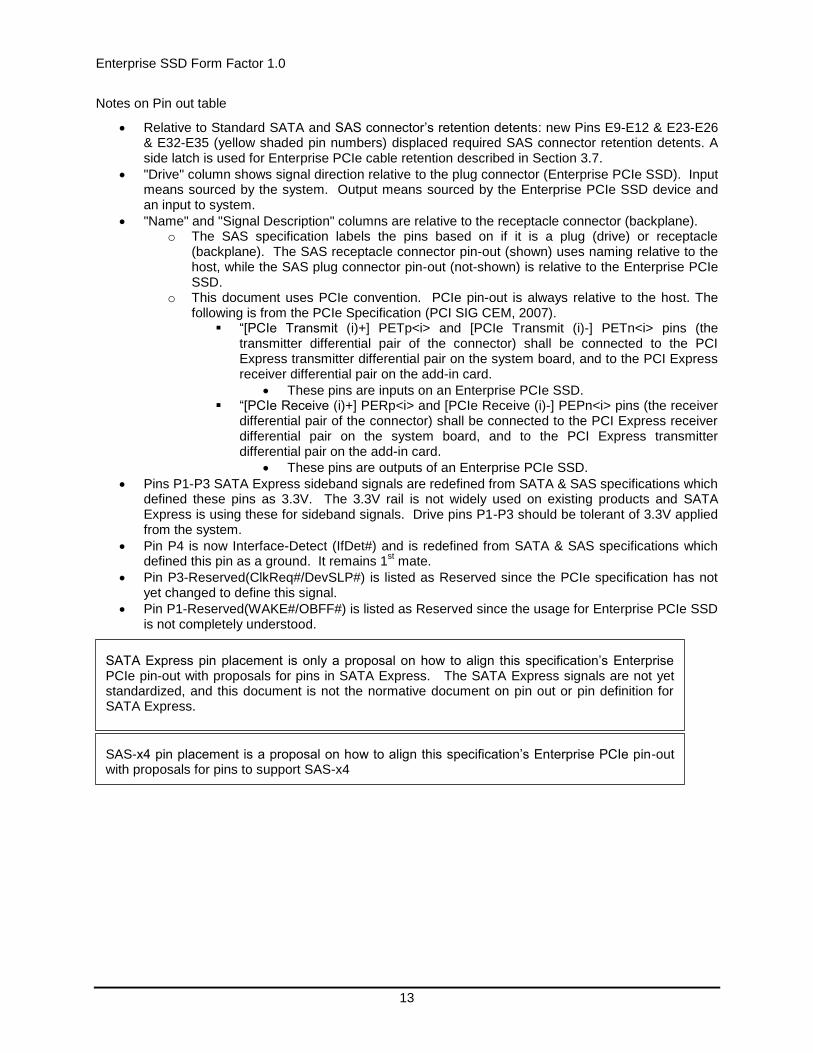
Notes on Pin out table
Relative to Standard SATA and SAS connector’s retention detents: new Pins E9-E12 & E23-E26 & E32-E35 (yellow shaded pin numbers) displaced required SAS connector retention detents. A side latch is used for Enterprise PCIe cable retention described in Section 3.7.
"Drive" column shows signal direction relative to the plug connector (Enterprise PCIe SSD). Input means sourced by the system. Output means sourced by the Enterprise PCIe SSD device and an input to system.
"Name" and "Signal Description" columns are relative to the receptacle connector (backplane). o The SAS specification labels the pins based on if it is a plug (drive) or receptacle
(backplane). The SAS receptacle connector pin-out (shown) uses naming relative to the host, while the SAS plug connector pin-out (not-shown) is relative to the Enterprise PCIe SSD.
o This document uses PCIe convention. PCIe pin-out is always relative to the host. The following is from the PCIe Specification (PCI SIG CEM, 2007).
“[PCIe Transmit (i)+] PETp<i> and [PCIe Transmit (i)-] PETn<i> pins (the transmitter differential pair of the connector) shall be connected to the PCI Express transmitter differential pair on the system board, and to the PCI Express receiver differential pair on the add-in card.
These pins are inputs on an Enterprise PCIe SSD. “[PCIe Receive (i)+] PERp<i> and [PCIe Receive (i)-] PEPn<i> pins (the receiver
differential pair of the connector) shall be connected to the PCI Express receiver differential pair on the system board, and to the PCI Express transmitter differential pair on the add-in card.
These pins are outputs of an Enterprise PCIe SSD.
Pins P1-P3 SATA Express sideband signals are redefined from SATA & SAS specifications which defined these pins as 3.3V. The 3.3V rail is not widely used on existing products and SATA Express is using these for sideband signals. Drive pins P1-P3 should be tolerant of 3.3V applied from the system.
Pin P4 is now Interface-Detect (IfDet#) and is redefined from SATA & SAS specifications which defined this pin as a ground. It remains 1
st mate.
Pin P3-Reserved(ClkReq#/DevSLP#) is listed as Reserved since the PCIe specification has not yet changed to define this signal.
Pin P1-Reserved(WAKE#/OBFF#) is listed as Reserved since the usage for Enterprise PCIe SSD is not completely understood.
SATA Express pin placement is only a proposal on how to align this specification’s Enterprise PCIe pin-out with proposals for pins in SATA Express. The SATA Express signals are not yet standardized, and this document is not the normative document on pin out or pin definition for SATA Express.
SAS-x4 pin placement is a proposal on how to align this specification’s Enterprise PCIe pin-out with proposals for pins to support SAS-x4

Enterprise SSD Form Factor 1.0
14
2.3 PRSNT# - Presence Detect and IfDet# - Interface Detect Signal Definition
The Presence (PRSNT#) is similar to Presence on the existing SFF-8482 connector. There is a redefinition of the IfDet# (pin P4) to encode drive type. The usage of the combined signals is to detect a drive is present and the drive type. Figure 6 shows how the drive type can be decoded from PRSNT# and IfDet# pins. .
Figure 6: Drive type - Pin decoding
P10 PRSNT#
Drive-output
P4 IfDet#
(was GND)
Drive-output
E39 DualPortEn#
Drive= Input
Comment
SATA/SAS Gnd (drv) Gnd (drv) Open(NC) Existing Drive (P4 is GND, E39 is NC)
SATA Express (Client PCIe)
Gnd (drv) Open (drv)1 Open(NC) PCIe on SATA/SAS lanes (S1-S14)
sPERst# is used, no RefClk used (P4 is NC, E39 is NC)
Enterprise PCIe (SFF-8639)
Open (drv) Gnd (drv) High (by system)
PCIe are on new Enterprise lanes (E7-E36) RefClk0 and ePERst0# are used
Dual Port Enterprise PCIe (SFF-8639)
Open (drv) Gnd (drv) Low (by system)
PCIe are on new Enterprise lanes (E7-E36) RefClk0, ePERst0#, and RefClk1, ePERst1# are used
No drive present
Open (drv) Open (drv) - All open
1. SATA Express may define IfDet# as a pull up & resistance. The SATA Express documentation is normative.
Either P10 or P4 being low indicates a drive is present. Further decoding is when P4 is open, then the PCIe lanes use the SATA pins (S1-S14) as defined for SATA Express.
In-band signal discovery is used to determine SATA vs. SAS. In-band signal discovery is used for width (x1, x2, x4) determination for SAS and PCIe. This is consistent with the existing SAS and PCIe standards.
2.4 DualPortEn# - PCIe Dual Port Enable
The Enterprise PCIe SSD can be configured to train as either a single x4 controller or dual x2. The mechanism for enabling dual port operation is DualPortEn# (pin E39). DualPortEn# is pulled high internal to the Enterprise PCIe SSD. If DualPortEn# is left open then the PCIe is configured as Single x4 port. If DualPortEn is pulled low by the system (driven low or grounded by backplane), then the Enterprise PCIe SSD has dual Ports enabled. DualPortEn# is part of the drive type determination shown in Figure 6.
DualPortEn# is a static signal. DualPortEn# must be stable 1uS before either ePERst[1:0]# are de-asserted, and DualPortEn# can only change if both ePERst[1:0]# are asserted. The Enterprise PCIe SSD may sample this signal at any time, and operation is undefined if DualPortEn# changes state during operation. In practice is sampled during Enterprise PCIe SSD local reset sequence to configure the ports.
The electrical signal characteristics of DualPortEn# follows the sideband interface signals of PCIe as stated in PCIe CEM Specification 2.6 Auxiliary Signal Parametric Specifications (PCI SIG CEM, 2007).

Enterprise SSD Form Factor 1.0
15
Section 5.1 on page 37 gives more details on Dual Port operation.
2.5 Reserved(WAKE#/OBFF#), Reserved(ClkReq#/DevSLP#)
The Reserved(Wake#/OBFF#), Reserved(ClkReq#/DevSLP#), signals are all optional and are used in device power management. These signals are defined by the PCIe Specification (PCI SIG ECNs, various). At this time the pin definition and usage in Enterprise PCIe SSD is not completely defined, so the pins are listed as reserved.
2.6 ePERst[1:0]# - PCIe Reset
The Enterprise PCIe Reset (ePERst[1:0]#) are logically the same as defined in the PCIe Specification (PCI SIG CEM, 2007) but for Enterprise PCIe SSD there are additional input current requirements. This allows for a drive to have pull up or pull down circuitry to support hot removal. This is defined in Section 7.3. There are two resets to allow for dual port operation, as defined in Section 5.
Enterprise SSD Form Factor 1.0
16
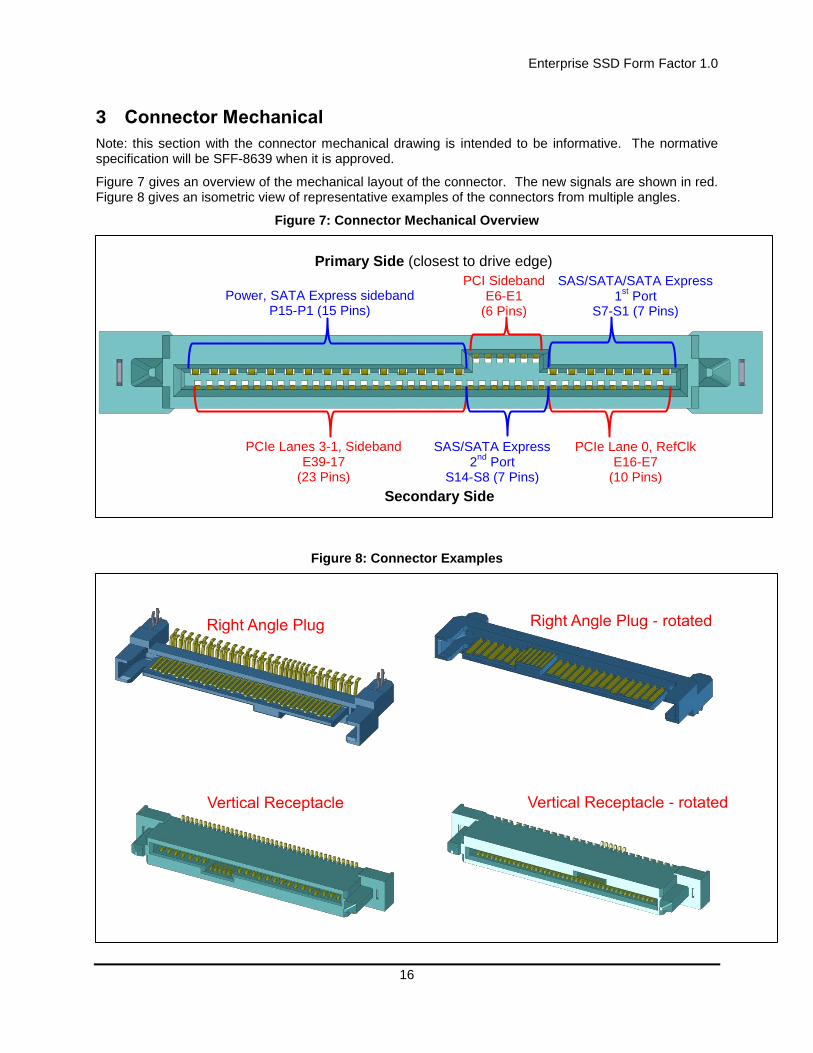
3 Connector Mechanical
Note: this section with the connector mechanical drawing is intended to be informative. The normative specification will be SFF-8639 when it is approved.
Figure 7 gives an overview of the mechanical layout of the connector. The new signals are shown in red. Figure 8 gives an isometric view of representative examples of the connectors from multiple angles.
Figure 7: Connector Mechanical Overview
Figure 8: Connector Examples
SAS/SATA/SATA Express 1
st Port
S7-S1 (7 Pins)
PCI Sideband E6-E1
(6 Pins)
Power, SATA Express sideband P15-P1 (15 Pins)
PCIe Lanes 3-1, Sideband E39-17
(23 Pins)
SAS/SATA Express 2
nd Port
S14-S8 (7 Pins)
PCIe Lane 0, RefClk E16-E7
(10 Pins)
Primary Side (closest to drive edge)
Secondary Side
Right Angle Plug - rotated Right Angle Plug
Vertical Receptacle Vertical Receptacle - rotated
Enterprise SSD Form Factor 1.0
17
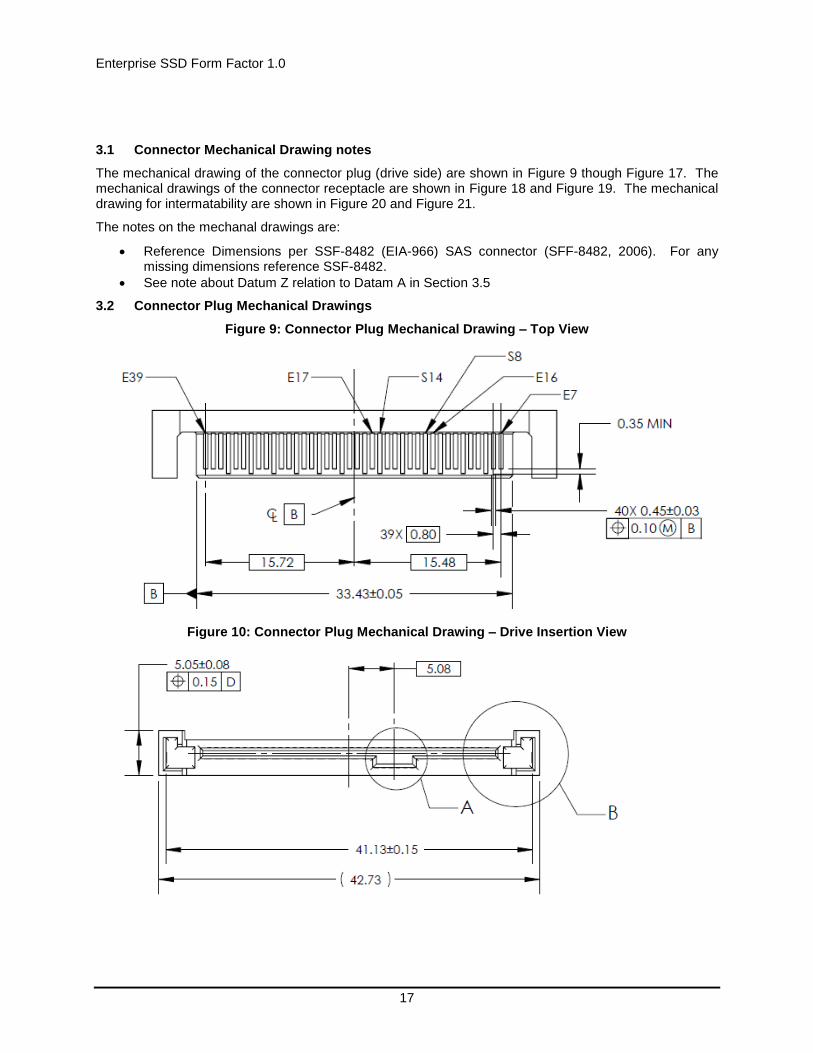
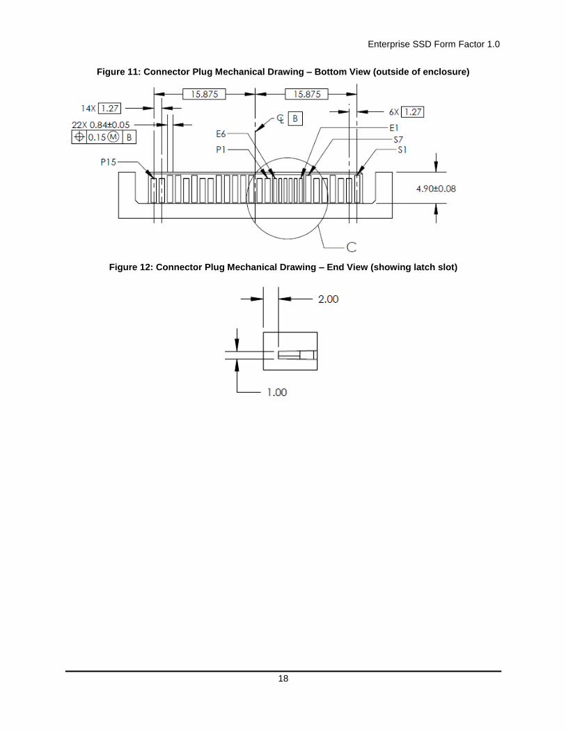
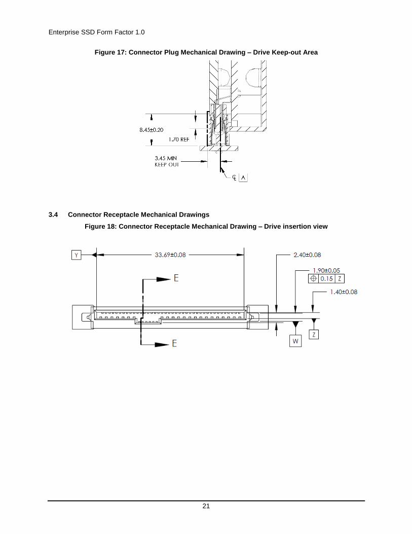
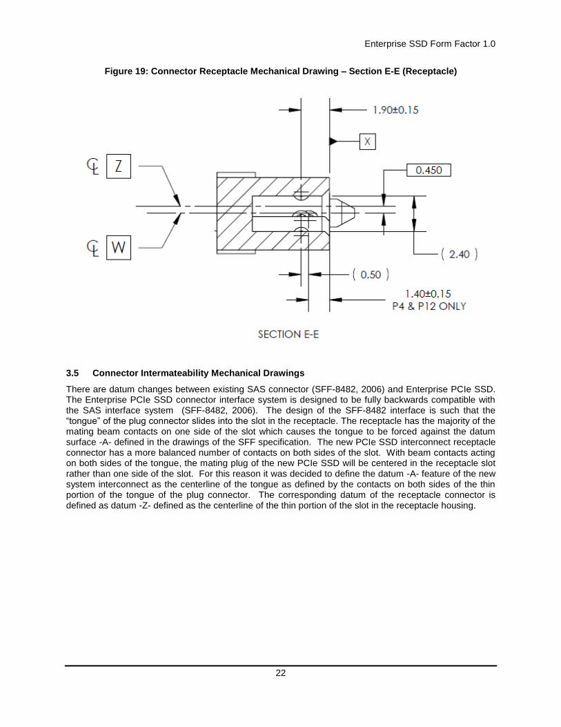
3.1 Connector Mechanical Drawing notes
The mechanical drawing of the connector plug (drive side) are shown in Figure 9 though Figure 17. The mechanical drawings of the connector receptacle are shown in Figure 18 and Figure 19. The mechanical drawing for intermatability are shown in Figure 20 and Figure 21.
The notes on the mechanal drawings are:
Reference Dimensions per SSF-8482 (EIA-966) SAS connector (SFF-8482, 2006). For any missing dimensions reference SSF-8482.
See note about Datum Z relation to Datam A in Section 3.5
3.2 Connector Plug Mechanical Drawings
Figure 9: Connector Plug Mechanical Drawing – Top View
Figure 10: Connector Plug Mechanical Drawing – Drive Insertion View
Enterprise SSD Form Factor 1.0
18
Figure 11: Connector Plug Mechanical Drawing – Bottom View (outside of enclosure)
Figure 12: Connector Plug Mechanical Drawing – End View (showing latch slot)
Enterprise SSD Form Factor 1.0
19
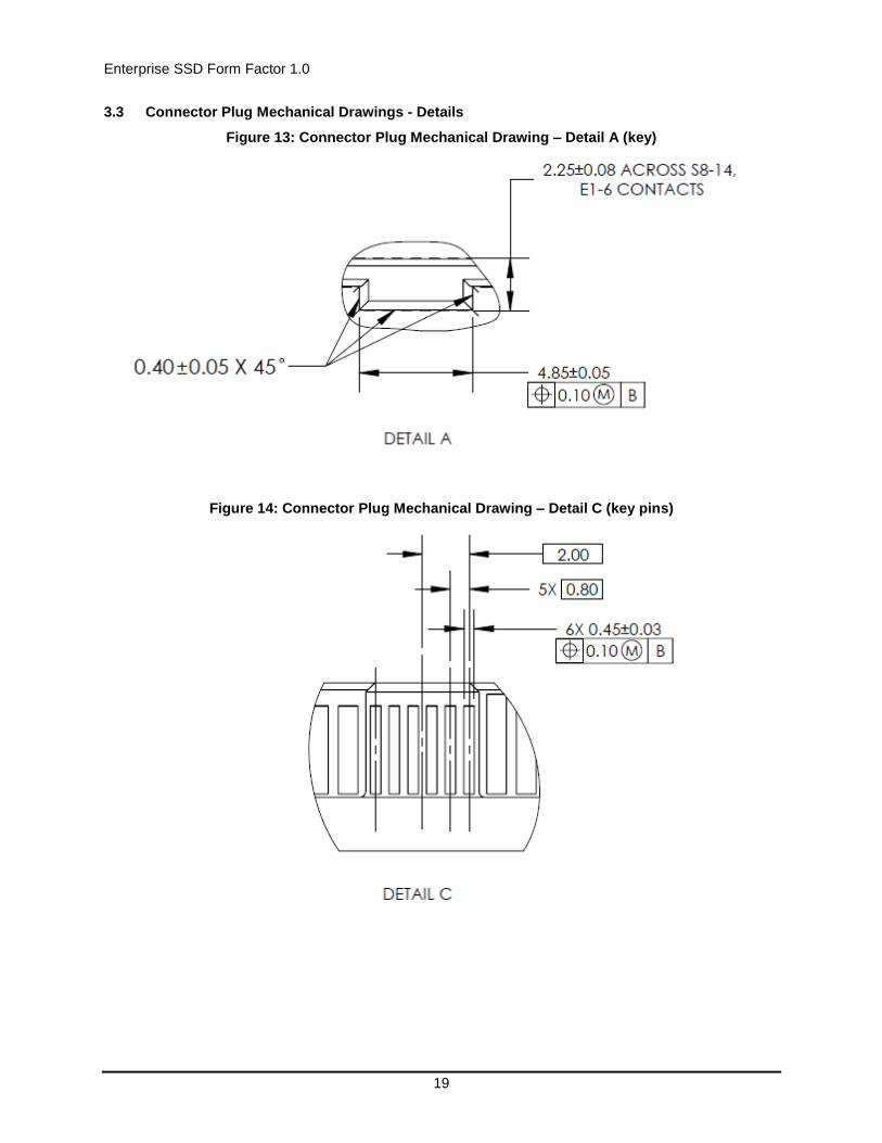
3.3 Connector Plug Mechanical Drawings - Details
Figure 13: Connector Plug Mechanical Drawing – Detail A (key)
Figure 14: Connector Plug Mechanical Drawing – Detail C (key pins)

Enterprise SSD Form Factor 1.0
20
Figure 15: Connector Plug Mechanical Drawing – Detail B (Tongue)
Figure 16: Connector Plug Mechanical Drawing – Section D-D (Tongue cross section)
Enterprise SSD Form Factor 1.0
21
Figure 17: Connector Plug Mechanical Drawing – Drive Keep-out Area
3.4 Connector Receptacle Mechanical Drawings
Figure 18: Connector Receptacle Mechanical Drawing – Drive insertion view
Enterprise SSD Form Factor 1.0
22
Figure 19: Connector Receptacle Mechanical Drawing – Section E-E (Receptacle)
3.5 Connector Intermateability Mechanical Drawings
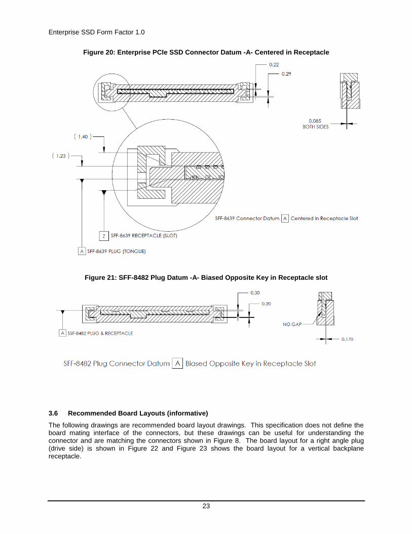
There are datum changes between existing SAS connector (SFF-8482, 2006) and Enterprise PCIe SSD. The Enterprise PCIe SSD connector interface system is designed to be fully backwards compatible with the SAS interface system (SFF-8482, 2006). The design of the SFF-8482 interface is such that the “tongue” of the plug connector slides into the slot in the receptacle. The receptacle has the majority of the mating beam contacts on one side of the slot which causes the tongue to be forced against the datum surface -A- defined in the drawings of the SFF specification. The new PCIe SSD interconnect receptacle connector has a more balanced number of contacts on both sides of the slot. With beam contacts acting on both sides of the tongue, the mating plug of the new PCIe SSD will be centered in the receptacle slot rather than one side of the slot. For this reason it was decided to define the datum -A- feature of the new system interconnect as the centerline of the tongue as defined by the contacts on both sides of the thin portion of the tongue of the plug connector. The corresponding datum of the receptacle connector is defined as datum -Z- defined as the centerline of the thin portion of the slot in the receptacle housing.
Enterprise SSD Form Factor 1.0
23
Figure 20: Enterprise PCIe SSD Connector Datum -A- Centered in Receptacle
Figure 21: SFF-8482 Plug Datum -A- Biased Opposite Key in Receptacle slot
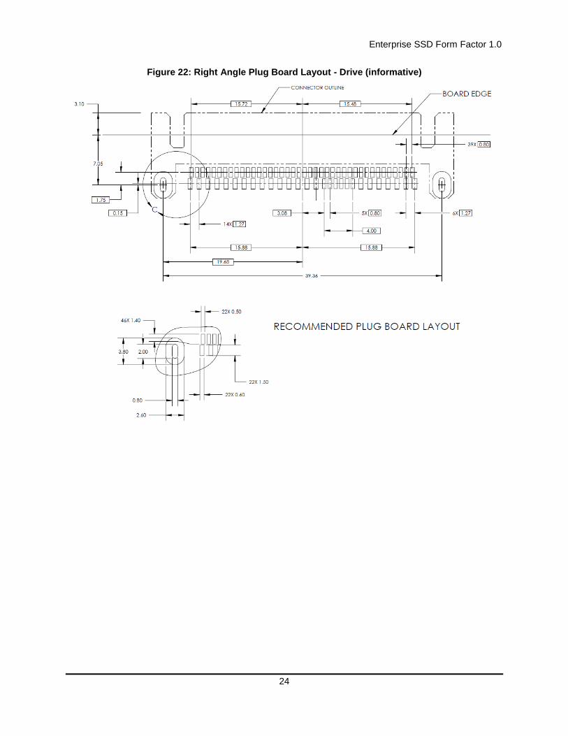
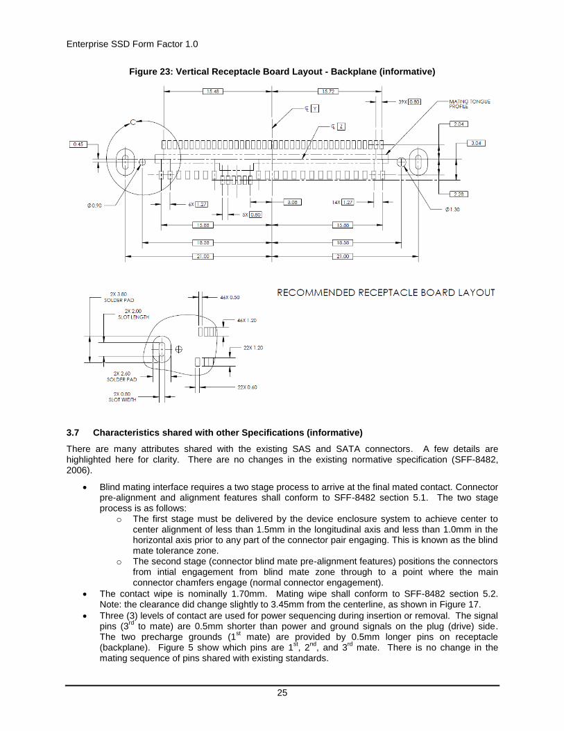
3.6 Recommended Board Layouts (informative)
The following drawings are recommended board layout drawings. This specification does not define the board mating interface of the connectors, but these drawings can be useful for understanding the connector and are matching the connectors shown in Figure 8. The board layout for a right angle plug (drive side) is shown in Figure 22 and Figure 23 shows the board layout for a vertical backplane receptacle.
Enterprise SSD Form Factor 1.0
24
Figure 22: Right Angle Plug Board Layout - Drive (informative)
Enterprise SSD Form Factor 1.0
25
Figure 23: Vertical Receptacle Board Layout - Backplane (informative)
3.7 Characteristics shared with other Specifications (informative)
There are many attributes shared with the existing SAS and SATA connectors. A few details are highlighted here for clarity. There are no changes in the existing normative specification (SFF-8482, 2006).
Blind mating interface requires a two stage process to arrive at the final mated contact. Connector pre-alignment and alignment features shall conform to SFF-8482 section 5.1. The two stage process is as follows:
o The first stage must be delivered by the device enclosure system to achieve center to center alignment of less than 1.5mm in the longitudinal axis and less than 1.0mm in the horizontal axis prior to any part of the connector pair engaging. This is known as the blind mate tolerance zone.
o The second stage (connector blind mate pre-alignment features) positions the connectors from intial engagement from blind mate zone through to a point where the main connector chamfers engage (normal connector engagement).
The contact wipe is nominally 1.70mm. Mating wipe shall conform to SFF-8482 section 5.2. Note: the clearance did change slightly to 3.45mm from the centerline, as shown in Figure 17.
Three (3) levels of contact are used for power sequencing during insertion or removal. The signal pins (3
rd to mate) are 0.5mm shorter than power and ground signals on the plug (drive) side.
The two precharge grounds (1st mate) are provided by 0.5mm longer pins on receptacle
(backplane). Figure 5 show which pins are 1st, 2
nd, and 3
rd mate. There is no change in the
mating sequence of pins shared with existing standards.
Enterprise SSD Form Factor 1.0
26
3.8 Cable Retention Mechanical Drawings
The primary server and storage Enterprise PCIe SSD connection is a backplane with retention provided by the drive carrier and storage enclosure. This is typically a universal driver carrier with insertion guides and insertion/ejection lever and any required keying. The definition of the drive carrier is outside the scope of this specification. The backplane receptacle connector is intended to be universal accepting all the standard drive keys, relying on more mechanically robust storage enclosure keying.
A cable receptacle is defined for applications needing a cabled interface to the drive. The Enterprise PCIe SSD cable (receptacle) interface incorporates an active latching retention mechanism to prevent accidental disconnecting of the interface. The cable retention is a snapping latch when mated and a press-to-release finger actuated button on the sides of the housing. This is different from existing SATA and SAS connectors which use a friction detent on the secondary side of the tongue. An overview of the Enterprise PCIe SSD cable retention is shown in Figure 24.
The Enterprise PCIe SSD cable (receptacle) has an extra keying feature to allow the Enterprise Cable to be blocked from mating with SATA, SATA Express, and SAS drives. The “L” shaped key shall be implemented on the Enterprise PCIe SSD cable receptacle. The “L” shaped key should not be implemented on the Enterprise PCIe SSD backplane receptacle. A keying compatibility matrix is shown in Section 10.3.
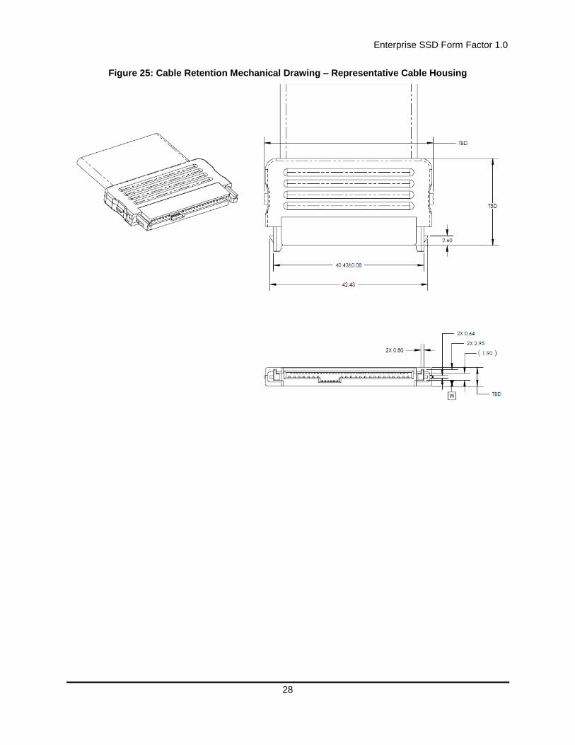
Figure 25 shows the mechanical drawing of the cable retention features that mate with the plug feature shown in Figure 12. The latch slot shall be implemented on Enterprise PCIe SSDs plugs. (The drive latch slot should not be implemented in SATA, SATA Express, and SAS drive plugs.) The latch shall be implemented on Enterprise PCIe SSD cables. The size cable housing and location of finger release are not specified, and these drawing are just informative. The clearance for a representative cable housing is shown in Figure 26. A representative cable assembly with flat ribbon cables is shown in Figure 27.
Implementation note: An existing SAS cable would accept an Enterprise PCIe SSD drive but would not function (no signal connections) and would have not engaged the SAS cable detent retention mechanism.

Enterprise SSD Form Factor 1.0
27
Figure 24: Cable Retention: Latch and Key Overview
Enterprise SSD Form Factor 1.0
28
Figure 25: Cable Retention Mechanical Drawing – Representative Cable Housing

Enterprise SSD Form Factor 1.0
29
Figure 26: Cable Release Clearance - Representative Cable Housing

Enterprise SSD Form Factor 1.0
30
Figure 27: Representative Cable Housing with flat ribbon cables
Enterprise SSD Form Factor 1.0
31
4 Hot Plug and Removal
Enterprise PCIe SSDs shall support hot plug and removal, both with and without prior system notification (surprise removal).
The fact that this is a physical hard drive form factor suggests that some characteristics of a hard drive usage model will be supported. In today’s servers hard drives are hot pluggable with some limitations. The Enterprise SSD drive shall be hot pluggable for both hot insertion and hot removal with and without prior system notification or preparation. Without prior system notification is typically referred to as “surprise insertion” and “surprise removal”.
Whether the user provides the system with notification of the hot plug event or not, many aspects of the system are involved in processing such an event. Elements of the overall system that are impacted are dependent on platform architecture and design but will typically include components of the PCIe infrastructure such as switches, platform firmware (BIOS), the Operating System’s PCIe bus driver stack and its IO stack. However, typically, a user would announce a hot plug event through one of the available system management interfaces.
The goal of this specification is not to define an overall systems architecture and design to support hot plug for the Enterprise PCIe SSDs but to define those elements of the hardware infrastructure that can be utilized to support such a solution.
The objectives of the hot plug design are:
To provide a user experience similar to existing disk drive hot plug behavior. Support all forms of hot insertion/removal
o OS aware insertion/removal o Surprise insertion/removal
Insertion
Insertion into a slot that has power and clocks on Removal
Removal from a slot that has power and clocks on
Removal with TLPs in flight and outstanding host non-posted requests o SAS based hot plug signaling or PCIe native hot-plug
No special controller requirements beyond those already defined in the PCIe base and in the PCIe Card Electromechanical specs
o Allows standard PCIe controllers to be used in Enterprise PCIe SSD without modification
The issues to be addressed are:
1. Limiting of inrush current. 2. Detection of Enterprise PCIe SSD addition and removal and Determination of Drive Type – PCIe
vs. SAS 3. Drive management – reset 4. SW implications
System support for Enterprise PCIe SSD hot plug and removal as well as the level of support (i.e., OS aware insertion/removal vs. OS and surprise insertion/removal) is implementation specific and outside the scope of this specification.
Implementation Note: Surprise Hot Removal is a must have requirement from system vendors for PCIe SSD devices. More specifically, it is expected that system vendors will require Enterprise PCIe SSD to retain all “committed data” following a surprise hot removal. This implies that the Enterprise PCIe SSD locally detect hot removal and store/destage any cache data. For a typical implementation this means the following is implemented
Having power sustaining capability, such as a battery or super cap. Detecting removal (by loss of 12V input or link loss)
Enterprise SSD Form Factor 1.0
32
Copying all “committed data” from volatile storage (DRAM based write back cache) to non-volatile storage. The details of this operation are complex, and implementation specific. The definition of “committed data” is specific to the higher level interface but typically means acknowledged write data. This “committed data” includes all indirection pointers to the data.
This copying of data has to be recovered upon PCIe SSD power on or hot addition. It is common for data or indirection tables to be written in to a staging location to simplify power down. This has to be reconstructed on power on/hot add to recover the full committed PCIe SSD state.
From a practical perspective for the Enterprise PCIe SSD, surprise hot removal is not that different from surprise power fail. In system power fail 12V likely has a longer power down ramp, but that is not guaranteed.
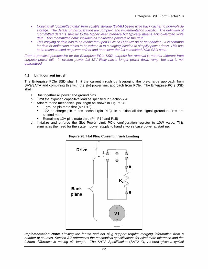
4.1 Limit current inrush
The Enterprise PCIe SSD shall limit the current inrush by leveraging the pre-charge approach from SAS/SATA and combining this with the slot power limit approach from PCIe. The Enterprise PCIe SSD shall:
a. Bus together all power and ground pins. b. Limit the exposed capacitive load as specified in Section 7.4. c. Adhere to the mechanical pin length as shown in Figure 28
1 ground pin mate first (pin P12) 12V precharge pin mates second (pin P13). In addition all the signal ground returns are
second mate. Remaining 12V pins mate third (Pin P14 and P15)
d. Initialize and enforce the Slot Power Limit PCIe configuration register to 10W value. This eliminates the need for the system power supply to handle worse case power at start up.
Figure 28: Hot Plug Current Inrush Limiting
Implementation Note: Limiting the inrush and hot plug support require merging information from a number of sources. Section 3.7 references the mechanical specifications for blind mate tolerance and the 0.5mm difference in mating pin length. The SATA Specification (SATA-IO, various) gives a typical

Enterprise SSD Form Factor 1.0
33
existing system insertion rates of 3ms delay from the 1st precharge 12V power to remaining power pins
contacting. Given these parameters and the 12Vcap specification in Section 7.4, the backplane resistance (RL in Figure 28) can be determined.
4.2 Detecting Enterprise PCIe SSD Insertion/Removal
There are multiple methods to detect PCIe SSD insertion or removal.
Use the drive type pins (PRSNT# pin P10, and IfDet#, pin P4). Note drive type can be determined as described in Section 2.3.
Use of In-Band signaling. The PCIe or SAS links may be enabled to train periodically, succeeding when device is plugged in. The PCIe or SAS links are lost when device is removed.
How system software is signaled is beyond the scope of this specification.
Implementation Note: There are three broad classes of usage of Presence (PRSNT#) and SATA Detect (IfDet#) during hot insertion or removal.
1. A common implementation is expected to be that PRSNT# and IfDet# are routed to the existing storage enclosure microcontroller and the microcontroller sends specific drive insertion or removal information to system software using the management stack. This is a common SAS implementation extended to two pins for 3 type encodings.
2. Alternatively the PRSNT# & IfDet# signals are simply turned into a general storage attention interrupt, enabling the system software to probe the system for changes. This can be augmented by examining if any PCIe link has changed status, or used as a trigger to enable Enterprise PCIe SSD to test for link training.
3. Optionally an existing storage enclosure microcontroller can poll and read the SM-bus to read vital product data (VPD) to learn specific information about the inserted device.
4. It is acceptable for the PRSNT# and IfDet# signals to be ignored completely by system hardware. Enterprise PCIe SSD insertion detection can be done in-band by detecting the training of the PCIe link. This may be complicated by PCIe links being disabled (powered down), so periodic re-arming may be required to probe for newly added Enterprise PCIe SSDs. In this case Enterprise PCIe SSD removal is detected by loss of PCIe link or PCIe link errors. From a timing perspective the PCIe link error/loss is the common 1
st detection of surprise removal since it is tightly coupled
with ongoing operation.
4.3 PCIe Hardware and Reset System Requirements
Enterprise PCIe SSD Reset/power on and PCIe Hot Add follows the PCIe specification (PCI SIG CEM, 2007). Enterprise PCIe SSDs must generate their own internal power-on reset by detecting the power ramp on 12V.
In all cases the Root Complex and system software shall allow at least 1.0 second after a Conventional Reset of an Enterprise PCIe SSD, before determining that an Enterprise PCIe SSD which fails to return a Successful Completion status for a valid Configuration Request, is an unresponsive or failed Enterprise PCIe SSD. This 1.0 second is true for both PCIe and SMbus operations. This period is independent of how quickly Link training completes.
PCIe Reset Card Requirements
● Normal System Operation (not Hot Insertion/Removal) o An Enterprise PCIe SSD shall adhere to PCIe system reset and card reset requirements
(Figure 29 and Figure 30) ● Hot Insertion
o If reset asserted then an Enterprise PCIe SSD must adhere to PCIe system reset and slot reset requirements.
This also means that the system & root complex must adhere to these requirements
o If reset negated Power and clock shall be stable 10ms after assertion of IfDet# (Enterprise PCIe
SSD’s Presence Detect)
Enterprise SSD Form Factor 1.0
34
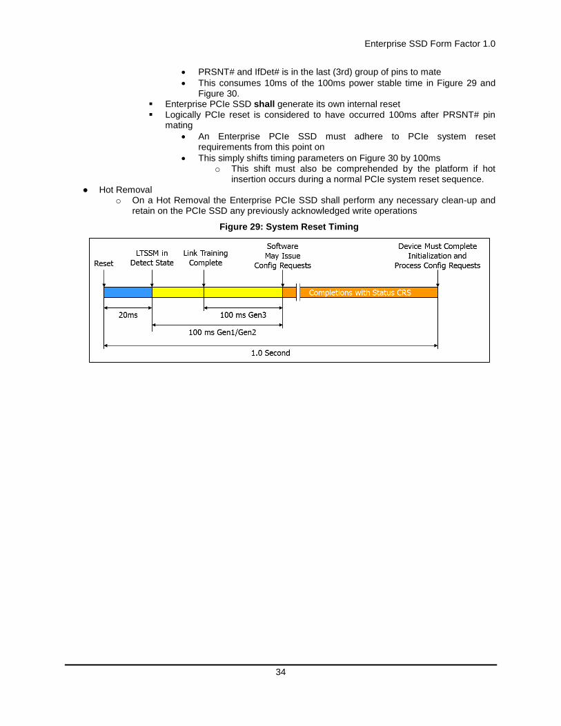
PRSNT# and IfDet# is in the last (3rd) group of pins to mate
This consumes 10ms of the 100ms power stable time in Figure 29 and Figure 30.
Enterprise PCIe SSD shall generate its own internal reset Logically PCIe reset is considered to have occurred 100ms after PRSNT# pin
mating
An Enterprise PCIe SSD must adhere to PCIe system reset requirements from this point on
This simply shifts timing parameters on Figure 30 by 100ms o This shift must also be comprehended by the platform if hot
insertion occurs during a normal PCIe system reset sequence. ● Hot Removal
o On a Hot Removal the Enterprise PCIe SSD shall perform any necessary clean-up and retain on the PCIe SSD any previously acknowledged write operations
Figure 29: System Reset Timing
Enterprise SSD Form Factor 1.0
35
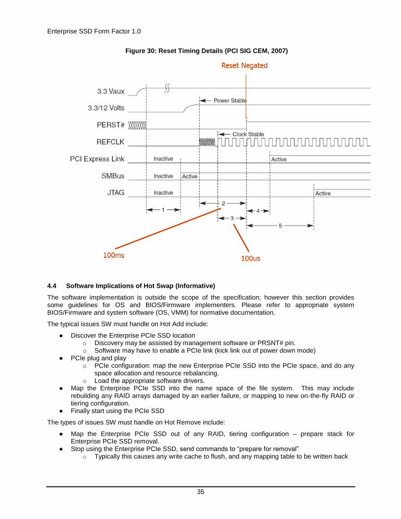
Figure 30: Reset Timing Details (PCI SIG CEM, 2007)
4.4 Software Implications of Hot Swap (Informative)
The software implementation is outside the scope of the specification; however this section provides some guidelines for OS and BIOS/Firmware implementers. Please refer to appropriate system BIOS/Firmware and system software (OS, VMM) for normative documentation.
The typical issues SW must handle on Hot Add include:
● Discover the Enterprise PCIe SSD location o Discovery may be assisted by management software or PRSNT# pin. o Software may have to enable a PCIe link (kick link out of power down mode)
● PCIe plug and play o PCIe configuration: map the new Enterprise PCIe SSD into the PCIe space, and do any
space allocation and resource rebalancing. o Load the appropriate software drivers.
● Map the Enterprise PCIe SSD into the name space of the file system. This may include rebuilding any RAID arrays damaged by an earlier failure, or mapping to new on-the-fly RAID or tiering configuration.
● Finally start using the PCIe SSD
The types of issues SW must handle on Hot Remove include:
● Map the Enterprise PCIe SSD out of any RAID, tiering configuration – prepare stack for Enterprise PCIe SSD removal.
● Stop using the Enterprise PCIe SSD, send commands to “prepare for removal” o Typically this causes any write cache to flush, and any mapping table to be written back
Enterprise SSD Form Factor 1.0
36
o If Enterprise PCIe SSD is not notified before removal, then it is surprise removal, see next section.
● Optionally use management system to identify the Enterprise PCIe SSD to remove. For example blink a red light for failure indication.
● User safely removes the Enterprise PCIe SSD.
If the removal is “surprise” meaning that the Enterprise PCIe SSD is active as it is being removed then the system software implications grow. These include, but are not limited to, the handling of errors during surprise removal event.
The software implications vary with the PCIe root port implementation and OS/SW versions. The software implications are beyond the scope of this specification.
Implementation Note: A complication of Hot Removal is discovering and testing all the boundary cases of the hardware/software interaction. In general a clean HW/SW interface and a clean software implementation are warranted – for example not a legacy interrupt model. The basic mechanism for an error detected by an instruction (ld/st) failure is to fault then handle the fault with by aborting the transfer.
It is expected that any data in flight at the time of removal is lost or corrupted. Hardware is only expected to retain “acknowledged and committed data”.
Implementation Note: It is expected that older versions of the operating system and PCIe root port will not be able to support surprise Hot Removal. With older OS/HW the errors during surprise removal might generate a fatal error.
New versions of the PCIe root port will be design to signal to the system software (BIOS and OS) to handle the hot removal event. The details are beyond the scope of this specification. The documents are not yet released. This detail is expected in documents such as the System BIOS Writers Guide for the root port component.
Implementation Note: Windows client OS is surprise hot remove capable because it was designed to support ExpressCard form factor. The Slot Capabilities Register contains a bit called Hot Plug Surprise which is a form factor specific bit. Express Card was expected to set this bit to indicate to Windows that card could be removed without notification and software stack should handle this without failure or data loss. For example, any writes to media behind such a card should never be cached by OS.
Since the Server OS shares a common code base with the Client OS at the kernel level, the basic capability exists in Windows Server but is not validated.
An outline of how Enterprise PCIe SSD Hot Swap will work:
- The OS gets signaled that an Enterprise PCIe SSD is inserted. (Using PCIe Hot Plug mechanism, a custom OEM leveraged mechanism, or detecting a change in PCIe Link Status.)
- OS enables read caching but not software write caching since the Enterprise PCIe SSD is surprise remove capable (if this impacts performance, then IT has to ensure they go through software UI to prep for ejection first).
- When the Enterprise PCIe SSD is removed cleanly, the error handling will abort any active transfers, then the presence detect toggle will indicate the hot remove event to OS
- OS will unload the corresponding driver stack and complete all pending IO request packets.

Enterprise SSD Form Factor 1.0
37
5 Dual Port Operation
The Enterprise PCIe SSD may optionally support Dual port operation. The expectation is that servers and other single controller systems will use Enterprise PCIe SSDs in a single x4 configuration. High Reliability Storage Controllers with redundant controllers will use two x2 links. In dual port mode the data on the Enterprise PCIe SSD is accessible from either controller allowing for failure of a controller. In dual port modes the Enterprise PCIe SSD acts independently as a PCIe device on each link. This is shown in Figure 31: Single Port and Dual Port example.
Implementation Note: Dual port operation is optional but is expected to be a required feature by storage vendors
Figure 31: Single Port and Dual Port example
.
The two PCIe links must operate independently. It is expected that both ports are fully PCIe compliant devices and as such each port presents a fully a PCIe compliant endpoint.
It is possible that the PCIe device is a multi-root PCIe switch, but that is not expected to be the common solution. In this solution resets and failures (such as errors and clock failures) on one port must not affect operation on the other port.
Implementation Note: In the most common dual port usage the Enterprise PCIe SSD appears as a totally independent Enterprise PCIe SSD on each bus sharing media. In Figure 31 both Controller A and Controller B see standard PCIe devices. There is not expected to be a PCIe-probe SW discoverable connection to the other port. There are two completely independent interfaces – such as two independent sets of PCIe configuration space, memory mapped control registers and queues. A higher level mechanism (such as reporting the same GUID on both links, or inherent knowledge of the topology) allow high level storage software to detect that the two Enterprise PCIe SSD controllers are sharing a common pool of storage and the higher level software coordinates the allocation of resources.
SSD Form Factor Device
(Enterprise PCIe SSD)
PCIe upstream
(e.g. CPU x4 PCIe port)
Conn
ecto
r
PCIe x4
SSD Form Factor Device
(Enterprise PCIe SSD)
Controller
A
Conn
ecto
r
PCIe x2
Typical Server configuration
Typical Storage configuration
Controller
B
PCIe x2
Cmd Q
Data Q Data Q
Data Q Data Q
Cmd Q
Data Q Data Q
Data Q Data Q
Cmd Q
Data Q Data Q
Data Q Data Q
Enterprise SSD Form Factor 1.0
38
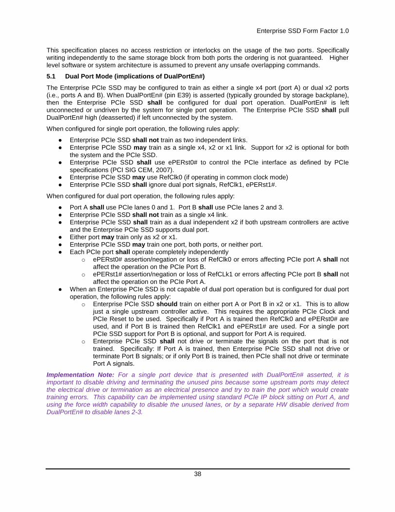
This specification places no access restriction or interlocks on the usage of the two ports. Specifically writing independently to the same storage block from both ports the ordering is not guaranteed. Higher level software or system architecture is assumed to prevent any unsafe overlapping commands.
5.1 Dual Port Mode (implications of DualPortEn#)
The Enterprise PCIe SSD may be configured to train as either a single x4 port (port A) or dual x2 ports (i.e., ports A and B). When DualPortEn# (pin E39) is asserted (typically grounded by storage backplane), then the Enterprise PCIe SSD shall be configured for dual port operation. DualPortEn# is left unconnected or undriven by the system for single port operation. The Enterprise PCIe SSD shall pull DualPortEn# high (deasserted) if left unconnected by the system.
When configured for single port operation, the following rules apply:
● Enterprise PCIe SSD shall not train as two independent links. ● Enterprise PCIe SSD may train as a single x4, x2 or x1 link. Support for x2 is optional for both
the system and the PCIe SSD. ● Enterprise PCIe SSD shall use ePERst0# to control the PCIe interface as defined by PCIe
specifications (PCI SIG CEM, 2007). ● Enterprise PCIe SSD may use RefClk0 (if operating in common clock mode) ● Enterprise PCIe SSD shall ignore dual port signals, RefClk1, ePERst1#.
When configured for dual port operation, the following rules apply:
● Port A shall use PCIe lanes 0 and 1. Port B shall use PCIe lanes 2 and 3. ● Enterprise PCIe SSD shall not train as a single x4 link. ● Enterprise PCIe SSD shall train as a dual independent x2 if both upstream controllers are active
and the Enterprise PCIe SSD supports dual port. ● Either port may train only as x2 or x1. ● Enterprise PCIe SSD may train one port, both ports, or neither port. ● Each PCIe port shall operate completely independently
o ePERst0# assertion/negation or loss of RefClk0 or errors affecting PCIe port A shall not affect the operation on the PCIe Port B.
o ePERst1# assertion/negation or loss of RefCLk1 or errors affecting PCIe port B shall not affect the operation on the PCIe Port A.
● When an Enterprise PCIe SSD is not capable of dual port operation but is configured for dual port operation, the following rules apply:
o Enterprise PCIe SSD should train on either port A or Port B in x2 or x1. This is to allow just a single upstream controller active. This requires the appropriate PCIe Clock and PCIe Reset to be used. Specifically if Port A is trained then RefClk0 and ePERst0# are used, and if Port B is trained then RefClk1 and ePERst1# are used. For a single port PCIe SSD support for Port B is optional, and support for Port A is required.
o Enterprise PCIe SSD shall not drive or terminate the signals on the port that is not trained. Specifically: If Port A is trained, then Enterprise PCIe SSD shall not drive or terminate Port B signals; or if only Port B is trained, then PCIe shall not drive or terminate Port A signals.
Implementation Note: For a single port device that is presented with DualPortEn# asserted, it is important to disable driving and terminating the unused pins because some upstream ports may detect the electrical drive or termination as an electrical presence and try to train the port which would create training errors. This capability can be implemented using standard PCIe IP block sitting on Port A, and using the force width capability to disable the unused lanes, or by a separate HW disable derived from DualPortEn# to disable lanes 2-3.
Enterprise SSD Form Factor 1.0
39
6 SM-Bus Operation
The Enterprise PCIe SSD should support SM-Bus operation. The SM-Bus protocol and signaling are defined in the SM-Bus Specification (SMBus, 2000).
SM-Bus is defined as independent of the PCIe links. There is no defined relationship between SM-Bus accesses and accesses on the PCIe buses.
There are two level of SM-Bus access.
1. Single reads and writes to a PROM device holding VPD (Vital Product Data) used for Enterprise PCIe SSD discovery and power allocation. Supported on 3.3Vaux power and during normal operation. The register definitions are listed in Section 9.1 SM-Bus Vital Product Data (VPD). Each Enterprise PCIe SSD’s VPD is expected to be independently addressed on a unique SM-Bus segment with VPD at a fixed address. SM-Bus ARP is not required for VPD access. An Enterprise PCIe SSD may require 3.3Vaux to be supplied to access this VPD data.
2. Extended management and access using MCTP-over-SMbus and this mode is only supported during normal operation (e.g., when 12V is present). MTCP Commands are defined in Section 9.2
Implementation Note: While SM-Bus is optional for Enterprise PCIe SSD operation, it is expected to be included in the Enterprise PCIe SSD purchase criteria by many system vendors.
Implementation note: This is specified to allow implementation with an I2C PROM connected to SM-Bus and to 3.3Vaux. It is allowed to have the VPD with 3.3Vaux applied but required to apply 12V to access optional extended management capabilities.
Implementation Note: The SM-Bus is not replicated for dual port operation. In dual controller configuration, this is envisioned as going to a shared management agent, using the multi-master characteristics of SM-Bus, or independent SM-Buses merged external to the Enterprise PCIe SSD.
6.1 Simple Accesses to Vital Product Data (VPD)
Enterprise PCIe SSD should support simple Reads and Write to Vital Product Data. This is defined in Section 9.1 SM-Bus Vital Product Data (VPD) in summary it contains:
Basic inventory information such as type and size of Enterprise PCIe SSD, manufacturer, date, revision, and GUID.
Power management data such as power level and power modes
Vendor specific data
Implementation note: This is likely implemented using a SM-Bus PROM connected to SM-Bus and to 3.3Vaux.
If a system vendor wants access to this data, then 3.3V shall be supplied to 3.3Vaux pins. If the system vendor does not want access to this data via SM-bus, then 3.3Vaux may be optional.
6.2 Extended SM-Bus management
An Enterprise PCIe SSD may support full MCTP device access over SMbus (MCTP-over-SMbus). This is only possible during normal operation (e.g. when 12V present).
The MCTP commands are beyond the scope of this specification.
Implementation Note:
The MCTP-over-SMbus is implementation dependent but is likely to support:
Access to VPD using MCTP semantics
Access to Enterprise PCIe SSD control registers
Access to underlying media (with protection mechanisms)
MCTP-over-SMbus is likely to be nearly symmetric with MCTP-over-PCIe.

Enterprise SSD Form Factor 1.0
40
7 Electrical (pointer to other specifications)
The electrical characteristics of signals that are defined as part of other standards, particularly PCIe and SAS, are referenced, rather than defined in this specification. This specification does define 2 signals, and new absolute maximum values for the 12V power specification. The new signal DualPortEn# complies with the PCIe auxiliary signal parametric specifications. The signals at Pins P1-P3 (Reserved(ClkReq#/DevSLP#), Reserved(Wake#/OBFF#)/SASAct2, sPERst#) shall be 3.3V tolerant.
Figure 4: Signal List Table (defining specification) on page 11 defines which specification is normative for each signal. This section gives electrical details on signals that are listed as “this spec” in Figure 4.
7.1 Electrical Channel
The high speed electrical characteristics of the connector are the same as the SAS Specification (T10, Various).
Implementation Note: There is ongoing work to get to higher frequencies and that will change the channel definition, and possibly the connector requirements. That is outside the scope of this specification.
Implementation Note: The electrical channel used in simulation is modeled after the typical server disks connection. The typical channel is shown in Figure 32. Itemizing the channel from the upstream PCIe transceiver toward the downstream Enterprise PCIe SSD port (letters correlate to Figure 32).
a. Upstream PCIe port transceiver and package b. Short (<3”) lead in trace between upstream PCIe device and cable connector. c. Internal cable – assuming a cable similar to SFF-8087 (SFF, various). The details are outside the
scope of this specification. d. Short (<4”) lead in trace between cable connector and Enterprise PCIe SSD connector e. Enterprise PCIe SSD connector – specified in this specification f. Short (<2”) trace inside Enterprise PCIe SSD g. Downstream PCIe port package and transceiver.
Figure 32: Typical SSD Form Factor Channel
7.2 Presence and Interface Detect
Presence and Interface Detect are used to signal the SSD has been inserted. This is the same purpose as SAS and SATA. The signal usage is given in Section 2.3 on page 14. In the drive the PRSNT# and IfDet# are connected to ground or left not-connected to signal drive type with a system supplying a pull up for signal detection.
Storage Backplane
SSD Form Factor Device
Motherboard or Adaptor
card
Conn
ecto
r
Xcr
Conn
Conn
ASIC
Cable
8 pairs + sideband
a b c
d
e
f
g
Enterprise SSD Form Factor 1.0
41
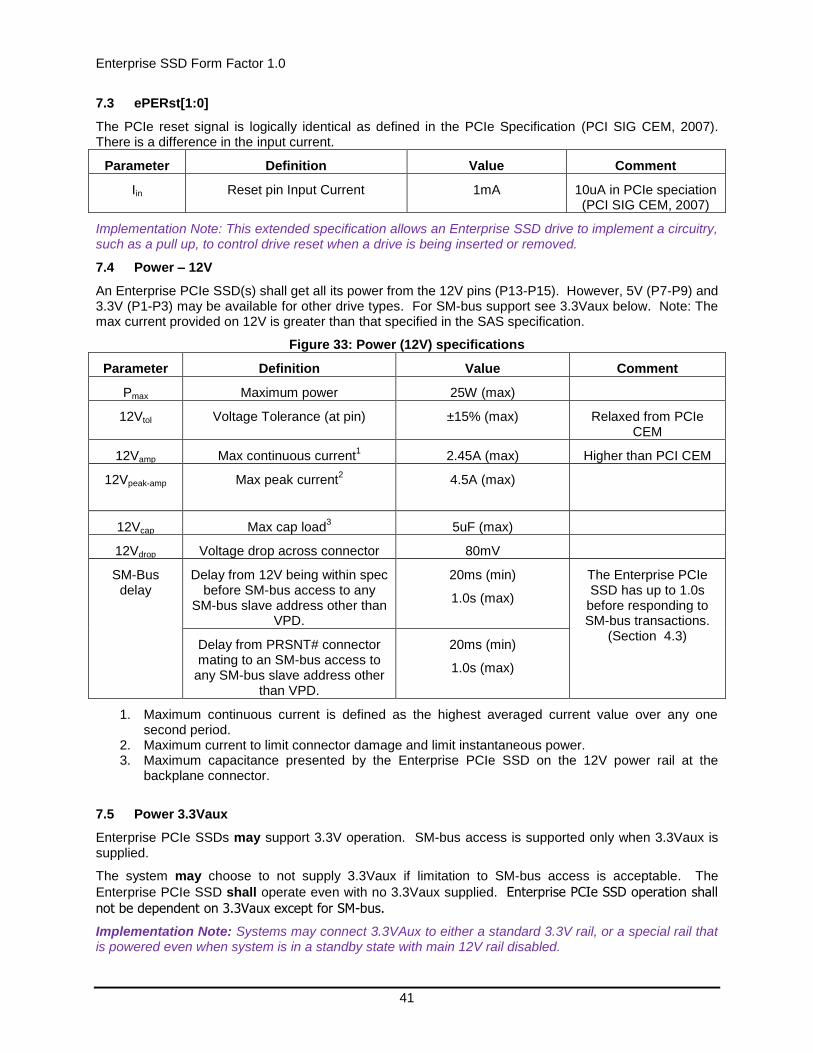
7.3 ePERst[1:0]
The PCIe reset signal is logically identical as defined in the PCIe Specification (PCI SIG CEM, 2007). There is a difference in the input current.
Parameter Definition Value Comment
Iin Reset pin Input Current 1mA 10uA in PCIe speciation (PCI SIG CEM, 2007)
Implementation Note: This extended specification allows an Enterprise SSD drive to implement a circuitry, such as a pull up, to control drive reset when a drive is being inserted or removed.
7.4 Power – 12V
An Enterprise PCIe SSD(s) shall get all its power from the 12V pins (P13-P15). However, 5V (P7-P9) and 3.3V (P1-P3) may be available for other drive types. For SM-bus support see 3.3Vaux below. Note: The max current provided on 12V is greater than that specified in the SAS specification.
Figure 33: Power (12V) specifications
Parameter Definition Value Comment
Pmax Maximum power 25W (max)
12Vtol Voltage Tolerance (at pin) ±15% (max) Relaxed from PCIe CEM
12Vamp Max continuous current1 2.45A (max) Higher than PCI CEM
12Vpeak-amp
Max peak current2
4.5A (max)
12Vcap Max cap load3 5uF (max)
12Vdrop Voltage drop across connector 80mV
SM-Bus delay
Delay from 12V being within spec before SM-bus access to any
SM-bus slave address other than VPD.
20ms (min)
1.0s (max)
The Enterprise PCIe SSD has up to 1.0s
before responding to SM-bus transactions.
(Section 4.3) Delay from PRSNT# connector mating to an SM-bus access to
any SM-bus slave address other than VPD.
20ms (min)
1.0s (max)
1. Maximum continuous current is defined as the highest averaged current value over any one second period.
2. Maximum current to limit connector damage and limit instantaneous power. 3. Maximum capacitance presented by the Enterprise PCIe SSD on the 12V power rail at the
backplane connector.
7.5 Power 3.3Vaux
Enterprise PCIe SSDs may support 3.3V operation. SM-bus access is supported only when 3.3Vaux is supplied.
The system may choose to not supply 3.3Vaux if limitation to SM-bus access is acceptable. The
Enterprise PCIe SSD shall operate even with no 3.3Vaux supplied. Enterprise PCIe SSD operation shall
not be dependent on 3.3Vaux except for SM-bus.
Implementation Note: Systems may connect 3.3VAux to either a standard 3.3V rail, or a special rail that is powered even when system is in a standby state with main 12V rail disabled.

Enterprise SSD Form Factor 1.0
42
Implementation Note: A typical Enterprise PCIe SSD could connect a small PROM to SM-Bus and power this device with 3.3Vaux. This VPD is only accessible if 3.3Vaux is applied by the system. SM-Bus could also be routed to the controller ASIC and these SM-bus operations would be dependent on 12V power rail.
Figure 34: Power 3.3VAux specifications
Parameter Definition Value Comment
3.3VAuxtol Voltage Tolerance (at pin) ±15% (max) Relaxed from PCIe CEM
3.3VAuxamp Max continuous current1 20µA
(SM-Bus inactive)
1mA (SM-Bus active)
Lower than PCI CEM
3.3VAuxcap Max cap load2 5µF (max)
SM-Bus delay Delay from 3.3V being within spec before SM-Bus access to VPD serial
EEPROM may be performed.
20ms (min)
1.0s (max)
The Enterprise PCIe SSD has up to 1.0s before responding to SM-bus transactions. (Section
4.3) Delay from PRSNT# & IfDet#
connector mating to when SM-bus access to VPD serial EEPROM may
be performed.
20ms (min)
1.0s (max)
1. Maximum continuous current is defined as the highest averaged current value over any one second period.
2. Maximum capacitance presented by the PCIe SSD on the 12V power rail at the backplane connector.
Enterprise SSD Form Factor 1.0
43
8 References and Bibliography
8.1 References
PCI Express® Specifications are available from http://www.pcisig.com.
PCI Express Base Specification, revision 3.0 (PCI SIG 3.0, 2010).
PCI Express Base Specification, revision 2.1 (PCI SIG 2.1, 2009).
PCI Express® Card Electromechanical Specification, Revision 2.0. April 11, 2007. Commonly known as the “PCIe CEM” spec (PCI SIG CEM, 2007).
PCI Express Engineering Change Notices, (PCI SIG ECNs, various) Small Form Factor (SFF) specifications are available from ftp://ftp.seagate.com/sff
SFF-8482 Specification for Unshielded Dual Port Serial Attachment Connector. Commonly known as the “SAS drive connector” and officially known as EIA-966. (SFF-8482, 2006)
SFF-8223 Specification for 2.5” Drive Form Factor with Serial Connector. Commonly known as the “2.5” drive” and officially known as EIA/ECA-720. (SFF-8223, 2007)
SFF-8301 Specification for 3.5” Drive Form Factor. Commonly known as the “3.5” drive” and officially known as EIA-740. (SFF-8223, 2007)
SSD HW/SW interface specification available from http://www.nvmexpress.org/ .
NVM Express (formerly eNVMHCI). This is the HW/SW interface for a PCIe based controller Non-Volatile (Flash, PCM) memory. Commonly known as “NVMe” (NVM Express, 2011),
8.2 References Under Development
The following are documents that are under development, but are not current publically available.
STA SAS3 WG – SCSI Trade Association’s Serial Attached SAS 3 generation Working Group. Defining a 12Gbps version for SAS disk standard. Commonly known as the “SAS3” (T10, SAS-3, 2011).
SATA Express. Defining a next generation of the SATA standard that uses PCIe interface for high performance drives. Also referred to in this specification as “Client PCIe” (SATA-IO, Draft 2011).
8.3 Formal Bibliography
NVM Express. (2011, July 12). NVM Express Revision 1.0b. Retrieved December 13, 2011, from NVM Express: http://www.nvmexpress.org/
PCI SIG 2.1. (2009, March 4). PCIe® Base Specification, Revision 2.1. Retrieved from PCI SIG: http://www.pcisig.com/specifications/pciexpress/
PCI SIG 3.0. (2010, November 10). PCIe® Base Specification Revision 3.0. Retrieved from PCI SIG: http://www.pcisig.com/specifications/pciexpress/
PCI SIG CEM. (2007, April 11). PCI Express® Card Electromechanical Specification Revision 2.0. Retrieved from PCI SIG: http://www.pcisig.com/specifications/pciexpress/
PCI SIG ECNs. (various). PCI Express Specifications & ECNs. Retrieved from PCI SIG: http://www.pcisig.com/specifications/pciexpress/specifications/#ecn2
PCI SIG. (various). PCI Express Specifications. Retrieved from PCI-SIG: http://www.pcisig.com/specifications/pciexpress
SATA IO. (2011, July). Serial ATA Revision 3.1 Specification. Retrieved from Serial ATA Internation Organization (SATA-IO): https://www.sata-io.org/developers/purchase_spec.asp
SATA IO. (Draft 2011, Not yet published). SATA Express. Retrieved from Serial ATA International Organization: https://www.sata-io.org/technology/sataexpress.asp
Enterprise SSD Form Factor 1.0
44
SATA IO. (various). SATA and SATA Express. Retrieved from Serial ATA Internation Organization (SATA-IO): http://www.sata-io.org/
SFF. (various). SFF Specifcations. Retrieved from Small Form Factor Web Site: http://ftp.seagate.com/sff
SFF-8223. (2007, February). EIA/ECA-720 - SPECIFICATION FOR SMALL FORM FACTOR 63.5 MM (2.5 INCH) DISK DRIVES. Retrieved from Electronic Components Association: http://global.ihs.com
SFF-8301. (1999, July). EIA-740 - SPECIFICATION FOR SMALL FORM FACTOR 88.9 MM (3.5 IN) DISK DRIVES. Retrieved from Electronic Components Association: http://global.ihs.com
SFF-8482. (2006, February 1). EIA-966, Serial Attachment 2X Unshielded Connector. Retrieved from SFF site in lieu of EIA: http://global.ihs.com, ftp://ftp.seagate.com/pub/sff/SFF-8482.PDF
SFF-8630. (Draft 2011). Serial Attachment Connector: 12 Gbps, Quad Port. Retrieved from SFF: ftp://ftp.seagate.com/sff/SFF-8630.PDF
SFF-8639. (Draft 2011). Serial Attachment/PCIe 12 Gbps 6X Unshielded Connector. Retrieved from SFF: ftp://ftp.seagate.com/sff/SFF-8639.PDF
SMBus. (2000, August 3). System Management Bus (SMBus) Specification. Retrieved from SM Bus: http://smbus.org/specs/smbus20.pdf
T10. (Various). INCITIS, Technical Committee T10 - SCSI Storage Interfaces. Retrieved from SCSI Storage Interfaces: http://www.t10.org
T10, SAS 2.1. (2011). ANSI/INCITS 478-2011, Serial Attached SCSI - 2.1 (SAS-2.1). Retrieved from INCITIS: http://www.techstreet.com/standards/incits/478_2011
T10, SAS-3. (2011, 11 11). Serial Attached SCSI - 3 (SAS-3). Retrieved from T10: http://www.t10.org/drafts.htm#SCSI3_SAS

Enterprise SSD Form Factor 1.0
45
9 SM-Bus - Informative Appendix
9.1 SM-Bus Vital Product Data (VPD)
VPD is at SM-Bus device address 0xA6.
Figure 35: SM Bus Vital Product Data
Addr Function Typ
e Size (B)
Default Value
Description Controlling Specification
0 Class Code RO 3 Vendor Device type and
programming interface
PCI Code and ID Assignment Specification
Rev. 1.0 (PCI-SIG) - Class Code
3
ID
RO 2 Vendor PCI-SIG Vendor ID
Enterprise NVMHCI Rev 1.0 - Identify Controller
Data Structure
5 RO 20 Vendor Serial Number
(vendor unique)
25 RO 40 Vendor Model Number (ASCII string)
65
PCIe Port 0 Capabilities
RO 1 Vendor Maximum Link Speed PCIe Base 3.0 (PCI-SIG) - Link Capabilities Register /
Maximum Link Width
66 RO 1 Vendor Maximum Link Width PCIe Base 3.0 (PCI-SIG) - Link Capabilities Register /
Max Link Speed
67
PCIe Port 1 Capabilities
RO 1 Vendor Maximum Link Speed PCIe Base 3.0 (PCI-SIG) - Link Capabilities Register /
Maximum Link Width
68 RO 1 Vendor Maximum Link Width PCIe Base 3.0 (PCI-SIG) - Link Capabilities Register /
Max Link Speed
69 Initial Power Requirement
s
RO 1 Vendor 12V power rail initial power requirement
(W)
70 RO 1 0 Reserved
71 RO 1 0 Reserved
72 Maximum Power
Requirements
RO 1 Vendor 12V power rail
maximum power requirement (W)
73 RO 1 0 Reserved
74 RO 1 0 Reserved
75 Capability
List Pointer RO 2 Vendor
16-bit address pointer to start of capability list (zero means no
capability list)
Enterprise SSD Form Factor 1.0
46
Figure 36: SM Bus Capability Definition
Capability List Headers are 4B in size
Next Capability Address of zero means last capability in list
Byte
3 2 1 0
Standard Capability
Next Capability Address
Capability ID
Byte
3 2 1 0
Vendor Specific Capability
Next Capability Address
0xA5
Vendor Specific PCI-SIG Vendor ID
9.2 SM-Bus Standard Capability definitions
The standard capability definitions are not yet specified. These are expected to include a standard way to identify extended capabilities such as MCTP capacities through a self-descriptive format.
9.3 SM-Bus MCTP commands
Not yet defined.
Enterprise SSD Form Factor 1.0
47
10 System Usage – Informative Appendix
There are multiple standards that use the same family of connectors – SAS and SATA standards, and emerging standards of Enterprise PCIe SSD (this specification), SATA Express, and SAS. This section gives an overview of how they interoperate.
10.1 Pin usage across standards
Figure 37 show the pin map across SATA and SAS connector to the Enterprise PCIe SSD. Figure 38 shows the pin map across connectors to the Enterprise PCIe SSD. The figures all use the Enterprise PCIe SSD signal names for consistency.
Implementation Note: There are multiple signals that are similar across the standards that are driven by system requirements. Even for signals that are logically the same there are multiple copies on the connector since the source or destination on the system design is not the same.
Existing SATA and existing SAS standards do not share high speed signals with Enterprise PCIe SSD. Only support signals are shared (12V, GND, PRSNT#, IfDet#). The SAS/SATA/SATA Express high speed signals are driven by separate SAS/SATA controllers from Enterprise PCIe ports.
SATA Express and Enterprise PCIe SSD standards do not share similar signals including separate high speed signals for PCIe lanes. This signal duplication is driven by the upstream connection. For SATA Express this is the SATA controller typically in a chipset or IO controller. For Enterprise PCIe SSD this is the highest performance PCIe root ports typically off a CPU or PCIe fan-out chipset.
o There are two sets of PCIe high speed signals for Lane 0 and 1. The SATA Express PCIe signals do not use the same wires as the Enterprise PCIe signals. The SATA Express needs the client PCIe to use the same signals as existing SATA (S1-S7). This allows the high speed pins to be reused in the cost constrained client systems. The Enterprise PCIe SSD uses separate signals (E7-E36) since these signals typically go direct to the PCIe root complex.
o There are independent PCIe Reset signals. SATA Express use pin P2 while Enterprise PCIe SSD use pin E5. This allows either controller to independently control the link reset. A controller may drive a reset output to enable simplified device reset.
o There is no PCI RefClk (+/-) for the SATA Express since this is after expected PCIe changes (a mode for greater skip order set insertion) to allow independent device and upstream clocking even with spread spectrum clock source.
o The Reserved(WAKE#/OBFF#) PCIe signal is shared, as are shared support 12V, Gnd, PRSNT#, IfDet#.
SAS-x4 and Enterprise PCIe SSD high speed signals are mixed – some separate and some shared. This prevents a flexible backplane from supporting Enterprise PCIe SSDs and SAS-x4 in one board, but connectors are mechanically compatible allowing shared components.
o The high speed data signals (lanes) are separate for SAS lanes 0-1 but shared for SAS lanes 2-3.
o SAS-x4 may optionally use new SATA Express support signals such as Reset (P2) o SAS-x4 may optionally use new Enterprise PCIe SSD support signals such as SM-Bus,
and 3.3Vaux.
SATA Express pin placement is only a proposal on how to align this specification’s Enterprise PCIe pin-out with proposals for pins in SATA Express. The SATA Express signals are not yet standardized, and this document is not the normative document on pin out or pin definition for SATA Express.
SAS-x4 pin placement is only a proposal on how to align this specification’s Enterprise
PCIe pin-out with proposals for pins to support SAS x4.

Enterprise SSD Form Factor 1.0
48
o SAS-x4 may redefine support pins for example layering a second Active (SAS-Active2) on existing Reserved(WAKE#/OBFF#) signal. If this is done the system must be able to gate the signal usage based on drive type.
Enterprise SSD Form Factor 1.0
49
Figure 37: Pin usage across Existing standards
Name Pin
GND S1
S0T+ (A+) S2
S0T- (A-) S3
GND S4
S0R- (B-) S5
S0R+ (B+) S6
GND S7
RefClk1+ E1
RefClk1- E2
3.3Vaux E3
ePERst1# E4
ePERst0# E5
RSVD E6
RSVD(Wake#) /SASAct2
P1
sPCIeRst/SAS P2
RSVD(DevSLP# P3
IfDet# P4
Ground P5
P6
5 V
P7
P8
P9
PRSNT# P10
Activity P11
Ground P12
12 V
P13
P14
P15
Pin Name
E7 RefClk0+
E8 RefClk0-
E9 GND
E10 PETp0
E11 PETn0
E12 GND
E13 PERn0
E14 PERp0
E15 GND
E16 RSVD
S8 GND
S9 S1T+
S10 S1T-
S11 GND
S12 S1R-
S13 S1R+
S14 GND
E17 RSVD
E18 GND
E19 PETp1/S2T+
E20 PETn1/S2T-
E21 GND
E22 PERn1/S2R-
E23 PERp1/S2R+
E24 GND
E25 PETp2/S3T+
E26 PETn2/S3T-
E27 GND
E28 PERn2/S3R-
E29 PERp2/S3R+
E30 GND
E31 PETp3
E32 PETn3
E33 GND
E34 PERn3
E35 PERp3
E36 GND
E37 SMClk
E38 SMDat
E39 DualPortEn#
SATA (existing)
Light=Optional
Orange=SATA
Gray=unused
Signal names do not match SATA spec
3.3
V
GN
D
Name Pin
GND S1
S0T+ (A+) S2
S0T- (A-) S3
GND S4
S0R- (B-) S5
S0R+ (B+) S6
GND S7
RefClk1+ E1
RefClk1- E2
3.3Vaux E3
ePERst1# E4
ePERst0# E5
RSVD E6
RSVD(Wake#) /SASAct2
P1
sPCIeRst/SAS P2
RSVD(DevSLP# P3
IfDet# P4
Ground P5
P6
5 V
P7
P8
P9
PRSNT# P10
Activity P11
Ground P12
12 V
P13
P14
P15
Pin Name
E7 RefClk0+
E8 RefClk0-
E9 GND
E10 PETp0
E11 PETn0
E12 GND
E13 PERn0
E14 PERp0
E15 GND
E16 RSVD
S8 GND
S9 S1T+
S10 S1T-
S11 GND
S12 S1R-
S13 S1R+
S14 GND
E17 RSVD
E18 GND
E19 PETp1/S2T+
E20 PETn1/S2T-
E21 GND
E22 PERn1/S2R-
E23 PERp1/S2R+
E24 GND
E25 PETp2/S3T+
E26 PETn2/S3T-
E27 GND
E28 PERn2/S3R-
E29 PERp2/S3R+
E30 GND
E31 PETp3
E32 PETn3
E33 GND
E34 PERn3
E35 PERp3
E36 GND
E37 SMClk
E38 SMDat
E39 DualPortEn#
SAS (existing)
Gray=unused
Purple-SAS
Light=Optional
3.3
V
GN
D
Name Pin
GND S1
S0T+ (A+) S2
S0T- (A-) S3
GND S4
S0R- (B-) S5
S0R+ (B+) S6
GND S7
RefClk1+ E1
RefClk1- E2
3.3Vaux E3
ePERst1# E4
ePERst0# E5
RSVD E6
RSVD(Wake#) /SASAct2
P1
sPCIeRst/SAS P2
RSVD(DevSLP# P3
IfDet# P4
Ground P5
P6
5 V
P7
P8
P9
PRSNT# P10
Activity P11
Ground P12
12 V
P13
P14
P15
Pin Name
E7 RefClk0+
E8 RefClk0-
E9 GND
E10 PETp0
E11 PETn0
E12 GND
E13 PERn0
E14 PERp0
E15 GND
E16 RSVD
S8 GND
S9 S1T+
S10 S1T-
S11 GND
S12 S1R-
S13 S1R+
S14 GND
E17 RSVD
E18 GND
E19 PETp1/S2T+
E20 PETn1/S2T-
E21 GND
E22 PERn1/S2R-
E23 PERp1/S2R+
E24 GND
E25 PETp2/S3T+
E26 PETn2/S3T-
E27 GND
E28 PERn2/S3R-
E29 PERp2/S3R+
E30 GND
E31 PETp3
E32 PETn3
E33 GND
E34 PERn3
E35 PERp3
E36 GND
E37 SMClk
E38 SMDat
E39 DualPortEn#
Enterprise PCIe (SFF-8639)
Dark=DaulP
Blue=sPCIe
Light=Optional
Gray=unused
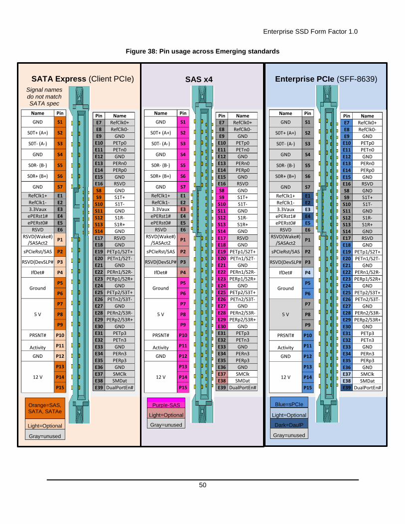
Enterprise SSD Form Factor 1.0
50
Figure 38: Pin usage across Emerging standards
Name Pin
GND S1
S0T+ (A+) S2
S0T- (A-) S3
GND S4
S0R- (B-) S5
S0R+ (B+) S6
GND S7
RefClk1+ E1
RefClk1- E2
3.3Vaux E3
ePERst1# E4
ePERst0# E5
RSVD E6
RSVD(Wake#) /SASAct2
P1
sPCIeRst/SAS P2
RSVD(DevSLP# P3
IfDet# P4
Ground P5
P6
5 V
P7
P8
P9
PRSNT# P10
Activity P11
GND P12
12 V
P13
P14
P15
Pin Name
E7 RefClk0+
E8 RefClk0-
E9 GND
E10 PETp0
E11 PETn0
E12 GND
E13 PERn0
E14 PERp0
E15 GND
E16 RSVD
S8 GND
S9 S1T+
S10 S1T-
S11 GND
S12 S1R-
S13 S1R+
S14 GND
E17 RSVD
E18 GND
E19 PETp1/S2T+
E20 PETn1/S2T-
E21 GND
E22 PERn1/S2R-
E23 PERp1/S2R+
E24 GND
E25 PETp2/S3T+
E26 PETn2/S3T-
E27 GND
E28 PERn2/S3R-
E29 PERp2/S3R+
E30 GND
E31 PETp3
E32 PETn3
E33 GND
E34 PERn3
E35 PERp3
E36 GND
E37 SMClk
E38 SMDat
E39 DualPortEn#
SATA Express (Client PCIe)
Light=Optional
Orange=SAS, SATA, SATAe
Gray=unused
Signal names do not match SATA spec
Name Pin
GND S1
S0T+ (A+) S2
S0T- (A-) S3
GND S4
S0R- (B-) S5
S0R+ (B+) S6
GND S7
RefClk1+ E1
RefClk1- E2
3.3Vaux E3
ePERst1# E4
ePERst0# E5
RSVD E6
RSVD(Wake#) /SASAct2
P1
sPCIeRst/SAS P2
RSVD(DevSLP# P3
IfDet# P4
Ground P5
P6
5 V
P7
P8
P9
PRSNT# P10
Activity P11
GND P12
12 V
P13
P14
P15
Pin Name
E7 RefClk0+
E8 RefClk0-
E9 GND
E10 PETp0
E11 PETn0
E12 GND
E13 PERn0
E14 PERp0
E15 GND
E16 RSVD
S8 GND
S9 S1T+
S10 S1T-
S11 GND
S12 S1R-
S13 S1R+
S14 GND
E17 RSVD
E18 GND
E19 PETp1/S2T+
E20 PETn1/S2T-
E21 GND
E22 PERn1/S2R-
E23 PERp1/S2R+
E24 GND
E25 PETp2/S3T+
E26 PETn2/S3T-
E27 GND
E28 PERn2/S3R-
E29 PERp2/S3R+
E30 GND
E31 PETp3
E32 PETn3
E33 GND
E34 PERn3
E35 PERp3
E36 GND
E37 SMClk
E38 SMDat
E39 DualPortEn#
SAS x4
Gray=unused
Purple-SAS
Light=Optional
Name Pin
GND S1
S0T+ (A+) S2
S0T- (A-) S3
GND S4
S0R- (B-) S5
S0R+ (B+) S6
GND S7
RefClk1+ E1
RefClk1- E2
3.3Vaux E3
ePERst1# E4
ePERst0# E5
RSVD E6
RSVD(Wake#) /SASAct2
P1
sPCIeRst/SAS P2
RSVD(DevSLP# P3
IfDet# P4
Ground P5
P6
5 V
P7
P8
P9
PRSNT# P10
Activity P11
GND P12
12 V
P13
P14
P15
Pin Name
E7 RefClk0+
E8 RefClk0-
E9 GND
E10 PETp0
E11 PETn0
E12 GND
E13 PERn0
E14 PERp0
E15 GND
E16 RSVD
S8 GND
S9 S1T+
S10 S1T-
S11 GND
S12 S1R-
S13 S1R+
S14 GND
E17 RSVD
E18 GND
E19 PETp1/S2T+
E20 PETn1/S2T-
E21 GND
E22 PERn1/S2R-
E23 PERp1/S2R+
E24 GND
E25 PETp2/S3T+
E26 PETn2/S3T-
E27 GND
E28 PERn2/S3R-
E29 PERp2/S3R+
E30 GND
E31 PETp3
E32 PETn3
E33 GND
E34 PERn3
E35 PERp3
E36 GND
E37 SMClk
E38 SMDat
E39 DualPortEn#
Enterprise PCIe (SFF-8639)
Dark=DaulP
Blue=sPCIe
Light=Optional
Gray=unused
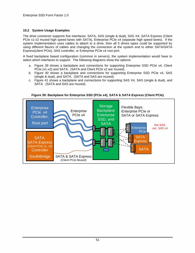
Enterprise SSD Form Factor 1.0
51
10.2 System Usage Examples
The drive connector supports five interfaces: SATA, SAS (single & dual), SAS X4, SATA Express (Client PCIe x1-x2 muxed high speed lanes with SATA), Enterprise PCIe x4 (separate high speed lanes). If the system implementation uses cables to attach to a drive, then all 5 drives types could be supported by using different flavors of cables and changing the connection at the system end to either SATA/SATA Express(client PCIe), SAS controller, or Enterprise PCIe x4 root port.
A fixed backplane based configuration (common in servers), the system implementation would have to select which interfaces to support. The following diagrams show the options:
a. Figure 39 shows a backplane and connections for supporting Enterprise SSD PCIe x4, Client PCIe (x1-x2) and SATA. (SATA and Client PCIe x2 are muxed).
b. Figure 40 shows a backplane and connections for supporting Enterprise SSD PCIe x4, SAS (single & dual), and SATA. (SATA and SAS are muxed).
c. Figure 41 shows a backplane and connections for supporting SAS X4, SAS (single & dual), and SATA. (SATA and SAS are muxed).
Figure 39: Backplane for Enterprise SSD (PCIe x4), SATA & SATA Express (Client PCIe)
Storage Backplane Enterprise SSD, and
SATA
SATA
SA
TA
Enterprise PCIe x4
SATA Express
x1-x2
X1
-x2
Enterprise PCIe
X4
SATA, SATA Express (Client PCIe x1, x2)
Controller
SouthBridge SATA & SATA Express (Client PCIe Muxed)
Flexible Bays: Enterprise PCIe or SATA or SATA Express
Enterprise PCIe x4
Controller,
Root port
New
N
ew
New
N
ew
Not SAS, not SAS x4
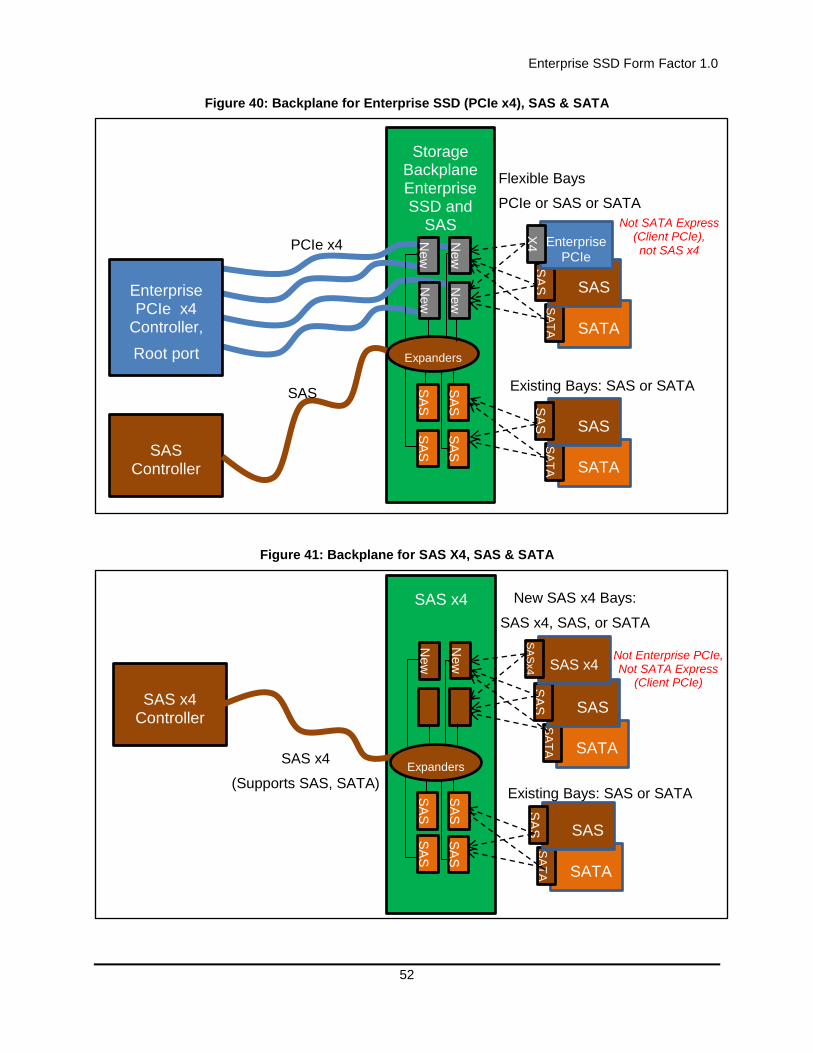
Enterprise SSD Form Factor 1.0
52
Figure 40: Backplane for Enterprise SSD (PCIe x4), SAS & SATA
Figure 41: Backplane for SAS X4, SAS & SATA
Storage Backplane Enterprise SSD and
SAS
SATA
SA
TA
PCIe x4
SAS S
AS
SAS Controller SATA
SA
TA
SAS
SA
S
Expanders S
AS
SA
S
SA
S
SA
S
New
N
ew
New
N
ew
SAS
Existing Bays: SAS or SATA
Flexible Bays
PCIe or SAS or SATA
Enterprise PCIe x4
Controller,
Root port
SAS x4
SATA
SA
TA
SAS
SA
S
SAS x4
SA
Sx4
SAS x4 Controller
SATA
SA
TA
SAS
SA
S
Expanders
SA
S
SA
S
SA
S
SA
S
N
ew
N
ew
SAS x4
(Supports SAS, SATA) Existing Bays: SAS or SATA
New SAS x4 Bays:
SAS x4, SAS, or SATA
Not SATA Express (Client PCIe), not SAS x4
Not Enterprise PCIe, Not SATA Express
(Client PCIe)
Enterprise PCIe
X4
Enterprise SSD Form Factor 1.0
53
10.3 Connector Keying (Informative)
The primary goal of connector keying is to make sure that end user pluggable devices and cables can be keyed to prevent insertion, if the device would not function.
Examples:
Block plugging of a SAS drive into client system with SATA and SATA Express cable. o Achieved by mechanical keys in region of pin E3-E4.
Block plugging of Enterprise PCIe SSD Cable into a SAS or SATA drive. o Achieved by cable keying in the alignment posts.
The standard must also support a universal backplane connector that allows any drive to mate. (Any keying is at the drive carrier or enclosure level.)
SATA Express keying features are only a proposal on how to align this specification’s with proposals for SATA Express. The SATA Express keying features are not yet standardized, and this document is not the normative document for SATA Express.

Enterprise SSD Form Factor 1.0
54
Figure 42 Cross Standard Connector Keying
SATA drive
SATA Express drive
SAS drive
Enterprise PCIe
drive
Enterprise backplane
Works- system supports
(carrier key)
Works- if system supports
(carrier key)
Works- if system supports
(carrier key) Works
SAS backplane
Works with STP Mates-Nonfunctional
(requires STP+) (carrier key)
Works Mates-nonfunctional
(carrier key)
SATA Express backplane/laptop
Works Works Blocked-Key Blocked-Key
SATA backplane/laptop
Blocked-Key Blocked-Key Blocked-Key
Enterprise cable
Blocked-Key
Blocked-Key
Blocked-Key
Works
SAS cable
Works Mates-Nonfunctional
(requires STP+) Works
Mates-nonfunctional & no detent retention
SATA Express cable
Works Blocked-Key Blocked-Key Blocked-Key
SATA cable
Works Blocked-Key Blocked-Key Blocked-Key
Key:
Works Works as expected
Works with STP Works as expected since SATA Tunnel Protocol widely deployed
Works if system supports Connectors will mate, will work if system designed to support - Section 10.2
Blocked-key Connectors do not mate, blocked by connector keying features Colored light green because this is desired behavior
Mates-nonfunctional Connector will mate, but will not function.
Carrier key Disk carrier is used, and system could be designed to prevent insertion
Enterprise SSD Form Factor 1.0
55
11 Specification Conventions
11.1 Definitions
11.1.1 PCI Express® (PCIe)
PCIe refer to the PCIe Express IO bus standards. Please see the 8.1 References on page 43 for a list of the most relevant PCIe documents (PCI SIG, various).
11.1.2 PCI Express® Generation 2 (PCIe Gen2)
In this context Gen 2 is used to refer to a link speed of 5Gbps using 8b/10b encoding.
11.1.3 PCI Express® Generation 3 (PCIe Gen3)
In this context Gen 3 is used to refer to a link speed 8Gbps using a 128/130 encoding with scrambling.
11.1.4 PCI Express® x4 (PCIe x4)
x4 means using 4 PCIe lanes for communication. This is 4 differential pairs in each direction. Total signals is 4 lanes times 2 (differential) times 2 (Transmit and receive) = 16 signals.
11.1.5 SFF standards
Small Form Factor Committee is an ad hoc group that defined the 2.5” & 3.5” drive and related specifications. Documents created by the SFF Committee are submitted to bodies such as EIA (Electronic Industries Association) or an ASC (Accredited Standards Committee).
Please see the 8.1 References on page 43 for a list of the most relevant (SFF, various).
11.1.6 SSD
Solid State Disk.
11.2 Keywords
Several keywords are used to differentiate between different levels of requirements.
11.2.1 mandatory
A keyword indicating items to be implemented as defined by this specification.
11.2.2 may
A keyword that indicates flexibility of choice with no implied preference.
11.2.3 optional
A keyword that describes features that are not required by this specification. However, if any optional feature defined by the specification is implemented, the feature shall be implemented in the way defined by the specification.
11.2.4 R, RSVD
“R” and RSVD are used as an abbreviation for “reserved” when the figure or table does not provide sufficient space for the full word “reserved”.
11.2.5 reserved
A keyword indicating reserved signal pins, bits, bytes, words, fields, and opcode values that are set-aside for future standardization. Their use and interpretation may be specified by future extensions to this or other specifications. A reserved bit, byte, word, field, or register shall be cleared to zero, or in accordance with a future extension to this specification. The recipient shall not check reserved bits, bytes, words, or fields.

Enterprise SSD Form Factor 1.0
56
11.2.6 shall
A keyword indicating a mandatory requirement. Designers are required to implement all such mandatory requirements to ensure interoperability with other products that conform to the specification.
11.2.7 should
A keyword indicating flexibility of choice with a strongly preferred alternative. Equivalent to the phrase “it is recommended”.


![SSD - ESOS LAB€¦ · SSD . 1 SSD Block Diagram 3.2 SSD NAND HDD . . SSD FTL . FTL NAND out-of-place update address mapping . Gabage Collection, Wear-leveling . 4. 4.1 SSD . Disksim[8]](https://img.pdfslide.net/doc/110x75/5ea6b67696cb1838a26c1ab1/ssd-esos-ssd-1-ssd-block-diagram-32-ssd-nand-hdd-ssd-ftl-ftl-nand-out-of-place.jpg)