Embed Size (px)
Citation preview

SOLOMON SYSTECH SEMICONDUCTOR TECHNICAL DATA
This document contains information on a new product. Specifications and information herein are subject to change without notice. http://www.solomon-systech.com SSD1305 Rev 1.8 P 1/71 Jul 2007 Copyright © 2007 Solomon Systech Limited
SSD1305
Advance Information
132 x 64 Dot Matrix OLED/PLED Segment/Common Driver with Controller

Solomon Systech Jul 2007 P 2/71 Rev 1.8 SSD1305
CONTENTS
1 GENERAL DESCRIPTION.................................................................................................... 7
2 FEATURES ............................................................................................................................... 7
3 ORDERING INFORMATION................................................................................................ 7
4 BLOCK DIAGRAM ................................................................................................................. 8
5 DIE PAD FLOOR PLAN ......................................................................................................... 9
6 PIN ARRANGEMENT .......................................................................................................... 12 6.1 SSD1305T6R1 PIN ASSIGNMENT.........................................................................................................................12 6.2 SSD1305T7R1 PIN ASSIGNMENT.........................................................................................................................14
7 PIN DESCRIPTION............................................................................................................... 16
8 FUNCTIONAL BLOCK DESCRIPTIONS ......................................................................... 18 8.1 MCU INTERFACE SELECTION...............................................................................................................................18 8.1.1 MCU Parallel 6800-series Interface...............................................................................................................18 8.1.2 MCU Parallel 8080-series Interface...............................................................................................................19 8.1.3 MCU Serial Interface......................................................................................................................................21 8.1.4 MCU I2C Interface..........................................................................................................................................21
8.2 COMMAND DECODER ..........................................................................................................................................24 8.3 OSCILLATOR CIRCUIT AND DISPLAY TIME GENERATOR......................................................................................25 8.4 FR SYNCHRONIZATION ........................................................................................................................................26 8.5 RESET CIRCUIT ....................................................................................................................................................26 8.6 SEGMENT DRIVERS / COMMON DRIVERS .............................................................................................................27 8.7 GRAPHIC DISPLAY DATA RAM (GDDRAM)......................................................................................................29 8.8 AREA COLOR DECODER.......................................................................................................................................30 8.9 SEG/COM DRIVING BLOCK ................................................................................................................................31 8.10 POWER ON AND OFF SEQUENCE .........................................................................................................................32 8.11 DC-DC CONVERTER ...........................................................................................................................................33
9 COMMAND TABLE.............................................................................................................. 35 9.1 DATA READ / WRITE ...........................................................................................................................................41
10 COMMAND DESCRIPTIONS ............................................................................................. 42 10.1 FUNDAMENTAL COMMAND .................................................................................................................................42 10.1.1 Set Lower Column Start Address for Page Addressing Mode (00h~0Fh) ......................................................42 10.1.2 Set Higher Column Start Address for Page Addressing Mode (10h~1Fh) .....................................................42 10.1.3 Set Memory Addressing Mode (20h)...............................................................................................................42 10.1.4 Set Column Address (21h) ..............................................................................................................................43 10.1.5 Set Page Address (22h)...................................................................................................................................44 10.1.6 Set Display Start Line (40h~7Fh) ...................................................................................................................45 10.1.7 Set Contrast Control for BANK0 (81h)...........................................................................................................45 10.1.8 Set Brightness for Area Color Banks (82h).....................................................................................................45 10.1.9 Set Look Up Table (LUT) (91h) .....................................................................................................................45 10.1.10 Set Bank Color of BANK1 to BANK16 (PAGE0) (92h) ..............................................................................46 10.1.11 Set Bank Color of BANK17 to BANK32 (PAGE0) (93h) ............................................................................46 10.1.12 Set Segment Re-map (A0h/A1h) ..................................................................................................................46 10.1.13 Entire Display ON (A4h/A5h) ...................................................................................................................46 10.1.14 Set Normal/Inverse Display (A6h/A7h).......................................................................................................46 10.1.15 Set Multiplex Ratio (A8h)............................................................................................................................46 10.1.16 Reserved (AAh) ...........................................................................................................................................46 10.1.17 Dim Mode setting (ABh) .............................................................................................................................46

SSD1305 Rev 1.8 P 3/71 Jul 2007 Solomon Systech
10.1.18 Master Configuration (ADh).......................................................................................................................46 10.1.19 Set Display ON/OFF (ACh/AEh/AFh) ........................................................................................................47 10.1.20 Set Page Start Address for Page Addressing Mode (B0h~B7h)..................................................................47 10.1.21 Set COM Output Scan Direction (C0h/C8h)...............................................................................................47 10.1.22 Set Display Offset (D3h) .............................................................................................................................47 10.1.23 Set Display Clock Divide Ratio/ Oscillator Frequency (D5h) ....................................................................50 10.1.24 Set Area Color Mode ON/OFF & Low Power Display Mode (D8h) ..........................................................50 10.1.25 Set Pre-charge Period (D9h) ......................................................................................................................50 10.1.26 Set COM Pins Hardware Configuration (DAh)..........................................................................................51 10.1.27 Set VCOMH Deselect Level (DBh) .................................................................................................................53 10.1.28 Enter Read Modify Write (E0h) ..................................................................................................................53 10.1.29 NOP (E3h) ..................................................................................................................................................54 10.1.30 Exit Read Modify Write (EEh) ....................................................................................................................54 10.1.31 Status register Read ....................................................................................................................................54
10.2 GRAPHIC ACCELERATION COMMAND..................................................................................................................55 10.2.1 Horizontal Scroll Setup (26h/27h) ..................................................................................................................55 10.2.2 Continuous Vertical and Horizontal Scroll Setup (29h/2Ah)..........................................................................56 10.2.3 Deactivate Scroll (2Eh)...................................................................................................................................57 10.2.4 Activate Scroll (2Fh).......................................................................................................................................57 10.2.5 Set Vertical Scroll Area(A3h) .........................................................................................................................58
11 MAXIMUM RATINGS.......................................................................................................... 59
12 DC CHARACTERISTICS..................................................................................................... 60
13 AC CHARACTERISTICS..................................................................................................... 61
14 APPLICATION EXAMPLE.................................................................................................. 66
15 PACKAGE INFORMATION................................................................................................ 67 15.1 SSD1305Z DIE TRAY INFORMATION...................................................................................................................67 15.2 SSD1305T6R1 DETAIL DIMENSION ....................................................................................................................68 15.3 SSD1305T7R1 DETAIL DIMENSION ....................................................................................................................70

Solomon Systech Jul 2007 P 4/71 Rev 1.8 SSD1305
TABLES TABLE 3-1 : ORDERING INFORMATION................................................................................................... 7 TABLE 5-1 : SSD1305Z BUMP DIE PAD COORDINATES....................................................................... 11 TABLE 6-1 : SSD1305T6R1 PIN ASSIGNMENT TABLE......................................................................... 13 TABLE 6-2 : SSD1305T7R1 PIN ASSIGNMENT .................................................................................... 15 TABLE 7-1 : PIN DESCRIPTION ............................................................................................................. 16 TABLE 7-2 : MCU BUS INTERFACE PIN SELECTION ............................................................................. 17 TABLE 8-1 : MCU INTERFACE ASSIGNMENT UNDER DIFFERENT BUS INTERFACE MODE........................ 18 TABLE 8-2 : CONTROL PINS OF 6800 INTERFACE .................................................................................. 18 TABLE 8-3 : CONTROL PINS OF 8080 INTERFACE (FORM 1) .................................................................. 20 TABLE 8-4 : CONTROL PINS OF 8080 INTERFACE (FORM 2) .................................................................. 20 TABLE 8-5 : CONTROL PINS OF SERIAL INTERFACE .............................................................................. 21 TABLE 8-6 : PASSIVE COMPONENT SELECTION ..................................................................................... 34 TABLE 9-1: COMMAND TABLE............................................................................................................. 35 TABLE 9-2 : READ COMMAND TABLE .................................................................................................. 41 TABLE 9-3 : ADDRESS INCREMENT TABLE (AUTOMATIC)..................................................................... 41 TABLE 10-1 : EXAMPLE OF SET DISPLAY OFFSET AND DISPLAY START LINE WITH NO REMAP ........... 48 TABLE 10-2 :EXAMPLE OF SET DISPLAY OFFSET AND DISPLAY START LINE WITH REMAP ................. 49 TABLE 10-3 : COM PINS HARDWARE CONFIGURATION....................................................................... 51 TABLE 10-4 : EXAMPLE OF READ MODIFY WRITE MODE .................................................................... 54 TABLE 11-1 : MAXIMUM RATINGS (VOLTAGE REFERENCED TO VSS) .................................................. 59 TABLE 12-1 : DC CHARACTERISTICS ................................................................................................... 60 TABLE 13-1 : AC CHARACTERISTICS ................................................................................................... 61 TABLE 13-2 : 6800-SERIES MCU PARALLEL INTERFACE TIMING CHARACTERISTICS.......................... 62 TABLE 13-3 : 8080-SERIES MCU PARALLEL INTERFACE TIMING CHARACTERISTICS.......................... 63 TABLE 13-4 : SERIAL INTERFACE TIMING CHARACTERISTICS .............................................................. 64 TABLE 13-5 :I2C INTERFACE TIMING CHARACTERISTICS ..................................................................... 65

SSD1305 Rev 1.8 P 5/71 Jul 2007 Solomon Systech
FIGURES FIGURE 4-1 : SSD1305 BLOCK DIAGRAM.............................................................................................. 8 FIGURE 5-1 : SSD1305Z DIE DRAWING................................................................................................. 9 FIGURE 5-2 : SSD1305Z ALIGNMENT MARKS DIMENSION.................................................................. 10 FIGURE 6-1 : SSD1305T6R1 PIN ASSIGNMENT ................................................................................... 12 FIGURE 6-2 : SSD1305T7R1 PIN ASSIGNMENT ................................................................................... 14 FIGURE 8-1 : DATA READ BACK PROCEDURE - INSERTION OF DUMMY READ......................................... 19 FIGURE 8-2 : EXAMPLE OF WRITE PROCEDURE IN 8080 PARALLEL INTERFACE MODE .......................... 19 FIGURE 8-3 : EXAMPLE OF READ PROCEDURE IN 8080 PARALLEL INTERFACE MODE............................ 19 FIGURE 8-4 : DISPLAY DATA READ BACK PROCEDURE - INSERTION OF DUMMY READ .......................... 20 FIGURE 8-5 : WRITE PROCEDURE IN SPI MODE..................................................................................... 21 FIGURE 8-6 : I2C-BUS DATA FORMAT................................................................................................... 22 FIGURE 8-7 : DEFINITION OF THE START AND STOP CONDITION........................................................... 23 FIGURE 8-8 : DEFINITION OF THE ACKNOWLEDGEMENT CONDITION..................................................... 24 FIGURE 8-9 : DEFINITION OF THE DATA TRANSFER CONDITION ........................................................... 24 FIGURE 8-10 : OSCILLATOR CIRCUIT AND DISPLAY TIME GENERATOR ............................................... 25 FIGURE 8-11 : SEGMENT OUTPUT WAVEFORM IN THREE PHASES......................................................... 27 FIGURE 8-12 : SEGMENT OUTPUT WAVEFORM FOR TWO DIFFERENT COLORS LUT SETTING................ 27 FIGURE 8-13 : EXAMPLE OF SEGMENT OUTPUT WAVEFORM OF MONOCHROME DISPLAY SECTION
UNDER MONOCHROME MODE......................................................................................................... 28 FIGURE 8-14 : EXAMPLE OF SEGMENT OUTPUT WAVEFORM OF AREA COLOR DISPLAY SECTION UNDER
AREA COLOR MODE........................................................................................................................ 28 FIGURE 8-15 : GDDRAM PAGES STRUCTURE OF SSD1305 ................................................................. 29 FIGURE 8-16 : ENLARGEMENT OF GDDRAM (NO ROW RE-MAPPING AND COLUMN-REMAPPING) ....... 29 FIGURE 8-17 : EXAMPLE OF AREA COLOR ASSIGNMENT ON A 132X64 OLED PANEL ........................... 30 FIGURE 8-18 : IREF CURRENT SETTING BY RESISTOR VALUE ............................................................... 31 FIGURE 8-19 : THE POWER ON SEQUENCE........................................................................................... 32 FIGURE 8-20 : THE POWER OFF SEQUENCE ......................................................................................... 32 FIGURE 8-21 : DC-DC VOLTAGE CONVERTER CIRCUIT ........................................................................ 33 FIGURE 10-1 : ADDRESS POINTER MOVEMENT OF PAGE ADDRESSING MODE ....................................... 42 FIGURE 10-2 : EXAMPLE OF GDDRAM ACCESS POINTER SETTING IN PAGE ADDRESSING MODE (NO
ROW AND COLUMN-REMAPPING) ................................................................................................... 42 FIGURE 10-3 : ADDRESS POINTER MOVEMENT OF HORIZONTAL ADDRESSING MODE........................... 43 FIGURE 10-4 : ADDRESS POINTER MOVEMENT OF VERTICAL ADDRESSING MODE ............................... 43 FIGURE 10-5 : EXAMPLE OF COLUMN AND ROW ADDRESS POINTER MOVEMENT................................ 44 FIGURE 10-6 : SEGMENT CURRENT VS CONTRAST SETTING.................................................................. 45 FIGURE 10-7 :TRANSITION BETWEEN DIFFERENT MODES ..................................................................... 47 FIGURE 10-8 : TYPICAL OSCILLATOR FREQUENCY ADJUSTMENT BY D5 COMMAND (VDD =2.8V)........ 50 FIGURE 10-9 : HORIZONTAL SCROLL EXAMPLE: SCROLL RIGHT BY 4 COLUMNS ................................ 55 FIGURE 10-10 : HORIZONTAL SCROLL EXAMPLE: SCROLL LEFT BY 2 COLUMNS ................................. 55 FIGURE 10-11 : HORIZONTAL SCROLLING SETUP EXAMPLE .................................................................. 55 FIGURE 10-12 : CONTINUOUS VERTICAL AND HORIZONTAL SCROLLING SETUP EXAMPLES.................. 56 FIGURE 10-13 : CONTINUOUS VERTICAL AND HORIZONTAL SCROLLING EXAMPLE: WITH SETTING IN
MUX RATIO .................................................................................................................................. 57 FIGURE 10-14 : VERTICAL SCROLL AREA SETUP EXAMPLES ................................................................. 58 FIGURE 13-1 : 6800-SERIES MCU PARALLEL INTERFACE CHARACTERISTICS ....................................... 62 FIGURE 13-2 : 8080-SERIES PARALLEL INTERFACE CHARACTERISTICS (FORM 1) ................................. 63 FIGURE 13-3 : 8080-SERIES PARALLEL INTERFACE CHARACTERISTICS (FORM 2) ................................. 63 FIGURE 13-4 : SERIAL INTERFACE CHARACTERISTICS .......................................................................... 64 FIGURE 13-5 : I2C INTERFACE TIMING CHARACTERISTICS ................................................................... 65

Solomon Systech Jul 2007 P 6/71 Rev 1.8 SSD1305
FIGURE 14-1 : APPLICATION EXAMPLE OF SSD1305T6R1 .................................................................. 66 FIGURE 15-1 SSD1305Z DIE TRAY INFORMATION ............................................................................... 67 FIGURE 15-2 SSD1305T6R1 DETAIL DIMENSION ............................................................................... 68 FIGURE 15-3 SSD1305T7R1 DETAIL DIMENSION ............................................................................... 70

SSD1305 Rev 1.8 P 7/71 Jul 2007 Solomon Systech
1 GENERAL DESCRIPTION The SSD1305 is a CMOS OLED/PLED driver with controller for organic/polymer light emitting diode dot-matrix graphic display system. It consists of 132 segments and 64 commons that can support a maximum display resolution of 132x64. There are 4-color selections to support monochrome or area color OLED/PLED. This IC is designed for Common Cathode type OLED panel. The SSD1305 embeds with contrast control, display RAM and oscillator, which reduces the number of external components and power consumption. It has 256-step brightness control and separate power for I/O interface logic. It is suitable for many compact portable applications, such as mobile phone sub-display, calculator and MP3 player, etc.
2 FEATURES • Resolution: 132 x 64 dot matrix panel • Area color support with 4 Color Selection and 64 steps per color • Power supply:
o VDD = 2.4V to 3.5V for IC logic o VCC = 7.0V to 15.0V for Panel driving o VDDIO = 1.6V to VDD for MCU interface
• Segment maximum source current: 320uA • Common maximum sink current: 45mA • Embedded 132 x 64 bit SRAM display buffer • 256-step Contrast Control • 8-bit 6800-series Parallel Interface, 8-bit 8080-series Parallel Interface, Serial Peripheral Interface,
I2C Interface • Row Re-mapping and Column Re-mapping • Continuous Horizontal, Vertical and Diagonal Scrolling • Dim Mode operations • Programmable Frame Frequency and Multiplexing Ratio • On-Chip Oscillator • DC-DC Controller embedded • Low power consumption • Wide range of operating temperatures: -40 to 85 °C
3 ORDERING INFORMATION
Table 3-1 : Ordering Information
Ordering Part Number SEG COM Package Form Reference Remark
SSD1305Z 132 64 Gold Bump Die Page 9, 67 • Min SEG pad pitch: 52um • Min COM pad pitch: 45um
SSD1305T6R1 132 64 TAB Page 12 ,68
• 35mm film, 4 sprocket hole • Folding TAB • 8-bit 80 / 8-bit 68 / SPI / I2C interface • SEG lead pitch 0.120mm x 0.998 =0.11976mm• COM lead pitch 0.120mm x 0.998 =0.11976mm
SSD1305T7R1 132 64 TAB Page 14, 70
• 35mm film, 4 sprocket hole • Folding TAB • 8-bit 80 / 8-bit 68 / SPI / I2C interface • SEG lead pitch 0.120mm x 0.998 =0.11976mm• COM lead pitch 0.120mm x 0.998 =0.11976mm

Solomon Systech Jul 2007 P 8/71 Rev 1.8 SSD1305
4 BLOCK DIAGRAM
Figure 4-1 : SSD1305 Block Diagram
M
CU
Inte
rfac
e
GD
DR
AM
Area
Col
orD
ecod
er
Com
mon
Driv
ers
Seg
men
tDriv
ers
Com
mon
Driv
ers
SEG
/CO
MD
rivin
gbl
ock
Osc
illat
or
Dis
play
Tim
ing
Gen
erat
or
Com
man
dD
ecod
er
(Eve
n)(o
dd)
RES#CS#
D/C#
BS[2:0]SCL/SCLK/D0
VCC
COM63COM61COM59... COM5COM3COM1
E(RD#) R/W#(WR#)
SDAIN/SDIN/D1SDAOUT/D2
D3D4D5D6D7
DC
-DC
Con
vert
er
VDD VDDIO VSS
VLSS
SEG131SEG130SEG129
.
.
.SEG2SEG1SEG0
COM0COM2COM4...COM58COM60COM62
CL
CL
S
FR
GD
R FB
VD
DB
VS
SB
V BR
EF
I RE
FV C
OM
H
SSD1305 Rev 1.8 P 9/71 Jul 2007 Solomon Systech
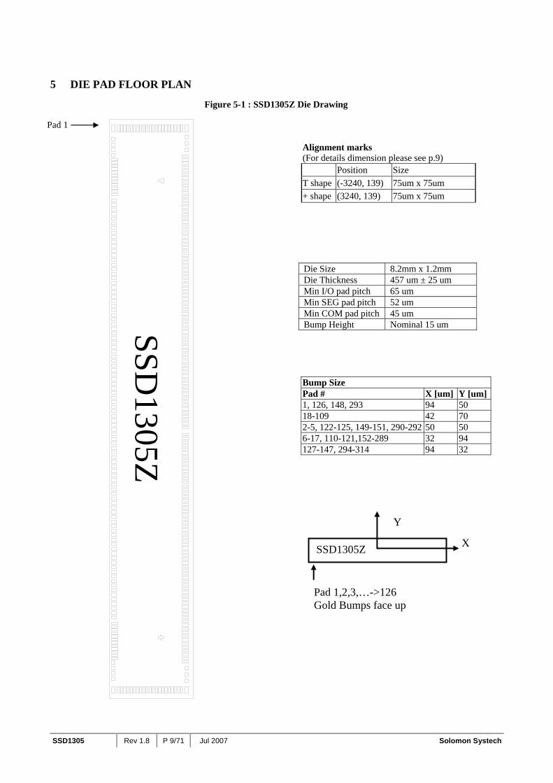
5 DIE PAD FLOOR PLAN
Figure 5-1 : SSD1305Z Die Drawing
Pad 1
Alignment marks (For details dimension please see p.9) Position Size T shape (-3240, 139) 75um x 75um + shape (3240, 139) 75um x 75um
Die Size 8.2mm x 1.2mm Die Thickness 457 um ± 25 um Min I/O pad pitch 65 um Min SEG pad pitch 52 um Min COM pad pitch 45 um Bump Height Nominal 15 um
Bump Size Pad # X [um] Y [um]1, 126, 148, 293 94 50 18-109 42 70 2-5, 122-125, 149-151, 290-292 50 50 6-17, 110-121,152-289 32 94 127-147, 294-314 94 32
Pad 1,2,3,…->126 Gold Bumps face up
SSD1305Z X
Y
SSD1305Z

Solomon Systech Jul 2007 P 10/71 Rev 1.8 SSD1305
Figure 5-2 : SSD1305Z Alignment Marks Dimension

SSD1305 Rev 1.8 P 11/71 Jul 2007 Solomon Systech
Table 5-1 : SSD1305Z Bump Die Pad Coordinates Pad no. Pad Name X-pos Y-pos Pad no. Pad Name X-pos Y-pos Pad no. Pad Name X-pos Y-pos Pad no. Pad Name X-pos Y-pos
1 NC -3980.5 -546.0 81 VDDIO 1137.5 -536.0 161 SEG6 3117.6 479.1 241 SEG86 -1091.2 479.12 NC -3821.5 -546.0 82 D0 1202.5 -536.0 162 SEG7 3065.7 479.1 242 SEG87 -1143.1 479.13 NC -3746.5 -546.0 83 D1 1267.5 -536.0 163 SEG8 3013.7 479.1 243 SEG88 -1195.1 479.14 NC -3671.5 -546.0 84 D2 1332.5 -536.0 164 SEG9 2961.7 479.1 244 SEG89 -1247.0 479.15 NC -3596.5 -546.0 85 D3 1397.5 -536.0 165 SEG10 2909.8 479.1 245 SEG90 -1299.0 479.16 COM53 -3537.5 -524.0 86 VSS 1462.5 -536.0 166 SEG11 2857.8 479.1 246 SEG91 -1351.0 479.17 COM54 -3492.5 -524.0 87 D4 1527.5 -536.0 167 SEG12 2805.9 479.1 247 SEG92 -1402.9 479.18 COM55 -3447.5 -524.0 88 D5 1592.5 -536.0 168 SEG13 2753.9 479.1 248 SEG93 -1454.9 479.19 COM56 -3402.5 -524.0 89 D6 1657.5 -536.0 169 SEG14 2701.9 479.1 249 SEG94 -1506.8 479.1
10 COM57 -3357.5 -524.0 90 D7 1722.5 -536.0 170 SEG15 2650.0 479.1 250 SEG95 -1558.8 479.111 COM58 -3312.5 -524.0 91 VSS 1787.5 -536.0 171 SEG16 2598.0 479.1 251 SEG96 -1610.8 479.112 COM59 -3267.5 -524.0 92 CLS 1852.5 -536.0 172 SEG17 2546.1 479.1 252 SEG97 -1662.7 479.113 COM60 -3222.5 -524.0 93 VDDIO 1917.5 -536.0 173 SEG18 2494.1 479.1 253 SEG98 -1714.7 479.114 COM61 -3177.5 -524.0 94 VDDIO 1982.5 -536.0 174 SEG19 2442.1 479.1 254 SEG99 -1766.6 479.115 COM62 -3132.5 -524.0 95 VDD 2047.5 -536.0 175 SEG20 2390.2 479.1 255 SEG100 -1818.6 479.116 COM63 -3087.5 -524.0 96 VDD 2112.5 -536.0 176 SEG21 2338.2 479.1 256 SEG101 -1870.6 479.117 NC -3042.5 -524.0 97 VDD 2177.5 -536.0 177 SEG22 2286.3 479.1 257 SEG102 -1922.5 479.118 NC -2957.5 -536.0 98 IREF 2242.5 -536.0 178 SEG23 2234.3 479.1 258 SEG103 -1974.5 479.119 VCC -2892.5 -536.0 99 VCOMH 2307.5 -536.0 179 SEG24 2182.3 479.1 259 SEG104 -2026.4 479.120 VCC -2827.5 -536.0 100 VCC 2372.5 -536.0 180 SEG25 2130.4 479.1 260 SEG105 -2078.4 479.121 VCC -2762.5 -536.0 101 VCC 2437.5 -536.0 181 SEG26 2078.4 479.1 261 SEG106 -2130.4 479.122 VCOMH -2697.5 -536.0 102 VCC 2502.5 -536.0 182 SEG27 2026.5 479.1 262 SEG107 -2182.3 479.123 VLSS -2632.5 -536.0 103 VCC 2567.5 -536.0 183 SEG28 1974.5 479.1 263 SEG108 -2234.3 479.124 VLSS -2567.5 -536.0 104 VCC 2632.5 -536.0 184 SEG29 1922.5 479.1 264 SEG109 -2286.2 479.125 VLSS -2502.5 -536.0 105 VCC 2697.5 -536.0 185 SEG30 1870.6 479.1 265 SEG110 -2338.2 479.126 VSS -2437.5 -536.0 106 VLSS 2762.5 -536.0 186 SEG31 1818.6 479.1 266 SEG111 -2390.2 479.127 VSS -2372.5 -536.0 107 VLSS 2827.5 -536.0 187 SEG32 1766.7 479.1 267 SEG112 -2442.1 479.128 TR11 -2307.5 -536.0 108 VLSS 2892.5 -536.0 188 SEG33 1714.7 479.1 268 SEG113 -2494.1 479.129 TR10 -2242.5 -536.0 109 NC 2957.5 -536.0 189 SEG34 1662.7 479.1 269 SEG114 -2546.0 479.130 TR9 -2177.5 -536.0 110 NC 3042.5 -524.0 190 SEG35 1610.8 479.1 270 SEG115 -2598.0 479.131 TR8 -2112.5 -536.0 111 COM31 3087.5 -524.0 191 SEG36 1558.8 479.1 271 SEG116 -2650.0 479.132 TR7 -2047.5 -536.0 112 COM30 3132.5 -524.0 192 SEG37 1506.9 479.1 272 SEG117 -2701.9 479.133 TR6 -1982.5 -536.0 113 COM29 3177.5 -524.0 193 SEG38 1454.9 479.1 273 SEG118 -2753.9 479.134 VSS -1917.5 -536.0 114 COM28 3222.5 -524.0 194 SEG39 1402.9 479.1 274 SEG119 -2805.8 479.135 TR5 -1852.5 -536.0 115 COM27 3267.5 -524.0 195 SEG40 1351.0 479.1 275 SEG120 -2857.8 479.136 TR4 -1787.5 -536.0 116 COM26 3312.5 -524.0 196 SEG41 1299.0 479.1 276 SEG121 -2909.8 479.137 TR3 -1722.5 -536.0 117 COM25 3357.5 -524.0 197 SEG42 1247.1 479.1 277 SEG122 -2961.7 479.138 TR2 -1657.5 -536.0 118 COM24 3402.5 -524.0 198 SEG43 1195.1 479.1 278 SEG123 -3013.7 479.139 TR1 -1592.5 -536.0 119 COM23 3447.5 -524.0 199 SEG44 1143.1 479.1 279 SEG124 -3065.6 479.140 TR0 -1527.5 -536.0 120 COM22 3492.5 -524.0 200 SEG45 1091.2 479.1 280 SEG125 -3117.6 479.141 VSS -1462.5 -536.0 121 COM21 3537.5 -524.0 201 SEG46 1039.2 479.1 281 SEG126 -3169.6 479.142 VSSB -1397.5 -536.0 122 NC 3596.5 -546.0 202 SEG47 987.3 479.1 282 SEG127 -3221.5 479.143 GDR -1332.5 -536.0 123 NC 3671.5 -546.0 203 SEG48 935.3 479.1 283 SEG128 -3273.5 479.144 GDR -1267.5 -536.0 124 NC 3746.5 -546.0 204 SEG49 883.3 479.1 284 SEG129 -3325.4 479.145 VDDB -1202.5 -536.0 125 NC 3821.5 -546.0 205 SEG50 831.4 479.1 285 SEG130 -3377.4 479.146 VDDB -1137.5 -536.0 126 NC 3980.5 -546.0 206 SEG51 779.4 479.1 286 SEG131 -3429.4 479.147 VDDB -1072.5 -536.0 127 COM20 3980.5 -468.4 207 SEG52 727.5 479.1 287 NC -3481.3 479.148 FB -1007.5 -536.0 128 COM19 3980.5 -423.4 208 SEG53 675.5 479.1 288 NC -3533.3 479.149 VBREF -942.5 -536.0 129 COM18 3980.5 -378.4 209 SEG54 623.5 479.1 289 NC -3585.2 479.150 BGGND -877.5 -536.0 130 COM17 3980.5 -333.4 210 SEG55 571.6 479.1 290 NC -3676.5 501.151 VSS -812.5 -536.0 131 COM16 3980.5 -288.4 211 SEG56 519.6 479.1 291 NC -3766.5 501.152 VDDB -747.5 -536.0 132 COM15 3980.5 -243.4 212 SEG57 467.7 479.1 292 NC -3856.5 501.153 VCIR -682.5 -536.0 133 COM14 3980.5 -198.4 213 SEG58 415.7 479.1 293 NC -3980.5 501.154 VCIR -617.5 -536.0 134 COM13 3980.5 -153.4 214 SEG59 363.7 479.1 294 COM32 -3980.5 431.655 VDD -552.5 -536.0 135 COM12 3980.5 -108.4 215 SEG60 259.8 479.1 295 COM33 -3980.5 386.656 VDD -487.5 -536.0 136 COM11 3980.5 -63.4 216 SEG61 207.9 479.1 296 COM34 -3980.5 341.657 VDD -422.5 -536.0 137 COM10 3980.5 -18.4 217 SEG62 155.9 479.1 297 COM35 -3980.5 296.658 VDD -357.5 -536.0 138 COM9 3980.5 26.6 218 SEG63 103.9 479.1 298 COM36 -3980.5 251.659 VDDIO -292.5 -536.0 139 COM8 3980.5 71.6 219 SEG64 52.0 479.1 299 COM37 -3980.5 206.660 VDDIO -227.5 -536.0 140 COM7 3980.5 116.6 220 SEG65 0.0 479.1 300 COM38 -3980.5 161.661 VDDIO -162.5 -536.0 141 COM6 3980.5 161.6 221 SEG66 -52.0 479.1 301 COM39 -3980.5 116.662 VCC -97.5 -536.0 142 COM5 3980.5 206.6 222 SEG67 -103.9 479.1 302 COM40 -3980.5 71.663 VCC -32.5 -536.0 143 COM4 3980.5 251.6 223 SEG68 -155.9 479.1 303 COM41 -3980.5 26.664 VCC 32.5 -536.0 144 COM3 3980.5 296.6 224 SEG69 -207.8 479.1 304 COM42 -3980.5 -18.465 VDDIO 97.5 -536.0 145 COM2 3980.5 341.6 225 SEG70 -259.8 479.1 305 COM43 -3980.5 -63.466 BS0 162.5 -536.0 146 COM1 3980.5 386.6 226 SEG71 -311.8 479.1 306 COM44 -3980.5 -108.467 VSS 227.5 -536.0 147 COM0 3980.5 431.6 227 SEG72 -363.7 479.1 307 COM45 -3980.5 -153.468 BS1 292.5 -536.0 148 NC 3980.5 501.1 228 SEG73 -415.7 479.1 308 COM46 -3980.5 -198.469 VDDIO 357.5 -536.0 149 NC 3856.5 501.1 229 SEG74 -467.6 479.1 309 COM47 -3980.5 -243.470 BS2 422.5 -536.0 150 NC 3766.5 501.1 230 SEG75 -519.6 479.1 310 COM48 -3980.5 -288.471 VSS 487.5 -536.0 151 NC 3676.5 501.1 231 SEG76 -571.6 479.1 311 COM49 -3980.5 -333.472 FR 552.5 -536.0 152 NC 3585.2 479.1 232 SEG77 -623.5 479.1 312 COM50 -3980.5 -378.473 CL 617.5 -536.0 153 NC 3533.3 479.1 233 SEG78 -675.5 479.1 313 COM51 -3980.5 -423.474 VSS 682.5 -536.0 154 NC 3481.3 479.1 234 SEG79 -727.4 479.1 314 COM52 -3980.5 -468.475 CS# 747.5 -536.0 155 SEG0 3429.4 479.1 235 SEG80 -779.4 479.176 RES# 812.5 -536.0 156 SEG1 3377.4 479.1 236 SEG81 -831.4 479.177 D/C# 877.5 -536.0 157 SEG2 3325.5 479.1 237 SEG82 -883.3 479.178 VSS 942.5 -536.0 158 SEG3 3273.5 479.1 238 SEG83 -935.3 479.179 R/W#(WR#) 1007.5 -536.0 159 SEG4 3221.5 479.1 239 SEG84 -987.2 479.180 E(RD#) 1072.5 -536.0 160 SEG5 3169.6 479.1 240 SEG85 -1039.2 479.1
Solomon Systech Jul 2007 P 12/71 Rev 1.8 SSD1305
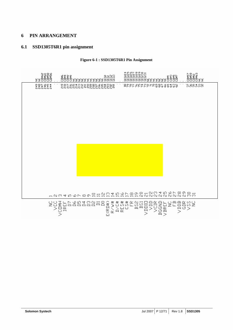
6 PIN ARRANGEMENT
6.1 SSD1305T6R1 pin assignment
Figure 6-1 : SSD1305T6R1 Pin Assignment

SSD1305 Rev 1.8 P 13/71 Jul 2007 Solomon Systech
Table 6-1 : SSD1305T6R1 Pin Assignment Table
Pin # Name Pin # Name Pin # Name Pin # Name1 NC 81 SEG123 161 SEG43 241 COM502 VCC 82 SEG122 162 SEG42 242 COM523 VCOMH 83 SEG121 163 SEG41 243 COM544 IREF 84 SEG120 164 SEG40 244 COM565 D7 85 SEG119 165 SEG39 245 COM586 D6 86 SEG118 166 SEG38 246 COM607 D5 87 SEG117 167 SEG37 247 COM628 D4 88 SEG116 168 SEG36 248 NC9 D3 89 SEG115 169 SEG35 249 NC10 D2 90 SEG114 170 SEG3411 D1 91 SEG113 171 SEG3312 D0 92 SEG112 172 SEG3213 E(RD#) 93 SEG111 173 SEG3114 R/W# 94 SEG110 174 SEG3015 D/C# 95 SEG109 175 SEG2916 RES# 96 SEG108 176 SEG2817 CS# 97 SEG107 177 SEG2718 FR 98 SEG106 178 SEG2619 BS2 99 SEG105 179 SEG2520 BS1 100 SEG104 180 SEG2421 VDDIO 101 SEG103 181 SEG2322 VDD 102 SEG102 182 SEG2223 VCIR 103 SEG101 183 SEG2124 BGGND 104 SEG100 184 SEG2025 VBREF 105 SEG99 185 SEG1926 NC 106 SEG98 186 SEG1827 FB 107 SEG97 187 SEG1728 VDDB 108 SEG96 188 SEG1629 GDR 109 SEG95 189 SEG1530 VSS 110 SEG94 190 SEG1431 NC 111 SEG93 191 SEG1332 NC 112 SEG92 192 SEG1233 NC 113 SEG91 193 SEG1134 COM63 114 SEG90 194 SEG1035 COM61 115 SEG89 195 SEG936 COM59 116 SEG88 196 SEG837 COM57 117 SEG87 197 SEG738 COM55 118 SEG86 198 SEG639 COM53 119 SEG85 199 SEG540 COM51 120 SEG84 200 SEG441 COM49 121 SEG83 201 SEG342 COM47 122 SEG82 202 SEG243 COM45 123 SEG81 203 SEG144 COM43 124 SEG80 204 SEG045 COM41 125 SEG79 205 NC46 COM39 126 SEG78 206 NC47 COM37 127 SEG77 207 NC48 COM35 128 SEG76 208 NC49 COM33 129 SEG75 209 NC50 COM31 130 SEG74 210 NC51 COM29 131 SEG73 211 NC52 COM27 132 SEG72 212 NC53 COM25 133 SEG71 213 NC54 COM23 134 SEG70 214 NC55 COM21 135 SEG69 215 NC56 COM19 136 SEG68 216 COM057 COM17 137 SEG67 217 COM258 COM15 138 SEG66 218 COM459 COM13 139 SEG65 219 COM660 COM11 140 SEG64 220 COM861 COM9 141 SEG63 221 COM1062 COM7 142 SEG62 222 COM1263 COM5 143 SEG61 223 COM1464 COM3 144 SEG60 224 COM1665 COM1 145 SEG59 225 COM1866 NC 146 SEG58 226 COM2067 NC 147 SEG57 227 COM2268 NC 148 SEG56 228 COM2469 NC 149 SEG55 229 COM2670 NC 150 SEG54 230 COM2871 NC 151 SEG53 231 COM3072 NC 152 SEG52 232 COM3273 SEG131 153 SEG51 233 COM3474 SEG130 154 SEG50 234 COM3675 SEG129 155 SEG49 235 COM3876 SEG128 156 SEG48 236 COM4077 SEG127 157 SEG47 237 COM4278 SEG126 158 SEG46 238 COM4479 SEG125 159 SEG45 239 COM4680 SEG124 160 SEG44 240 COM48

Solomon Systech Jul 2007 P 14/71 Rev 1.8 SSD1305
6.2 SSD1305T7R1 pin assignment
Figure 6-2 : SSD1305T7R1 Pin Assignment

SSD1305 Rev 1.8 P 15/71 Jul 2007 Solomon Systech
Table 6-2 : SSD1305T7R1 Pin Assignment Pin # Name Pin # Name Pin # Name Pin # Name
1 NC 81 SEG123 161 SEG43 241 COM502 VCC 82 SEG122 162 SEG42 242 COM523 VCOMH 83 SEG121 163 SEG41 243 COM544 IREF 84 SEG120 164 SEG40 244 COM565 D7 85 SEG119 165 SEG39 245 COM586 D6 86 SEG118 166 SEG38 246 COM607 D5 87 SEG117 167 SEG37 247 COM628 D4 88 SEG116 168 SEG36 248 NC9 D3 89 SEG115 169 SEG35 249 NC
10 D2 90 SEG114 170 SEG3411 D1 91 SEG113 171 SEG3312 D0 92 SEG112 172 SEG3213 E/RD# 93 SEG111 173 SEG3114 R/W# 94 SEG110 174 SEG3015 D/C# 95 SEG109 175 SEG2916 RES# 96 SEG108 176 SEG2817 CS# 97 SEG107 177 SEG2718 NC 98 SEG106 178 SEG2619 BS2 99 SEG105 179 SEG2520 BS1 100 SEG104 180 SEG2421 VDD 101 SEG103 181 SEG2322 NC 102 SEG102 182 SEG2223 NC 103 SEG101 183 SEG2124 NC 104 SEG100 184 SEG2025 VBREF 105 SEG99 185 SEG1926 NC 106 SEG98 186 SEG1827 FB 107 SEG97 187 SEG1728 VDDB 108 SEG96 188 SEG1629 GDR 109 SEG95 189 SEG1530 VSS 110 SEG94 190 SEG1431 NC 111 SEG93 191 SEG1332 NC 112 SEG92 192 SEG1233 NC 113 SEG91 193 SEG1134 COM63 114 SEG90 194 SEG1035 COM61 115 SEG89 195 SEG936 COM59 116 SEG88 196 SEG837 COM57 117 SEG87 197 SEG738 COM55 118 SEG86 198 SEG639 COM53 119 SEG85 199 SEG540 COM51 120 SEG84 200 SEG441 COM49 121 SEG83 201 SEG342 COM47 122 SEG82 202 SEG243 COM45 123 SEG81 203 SEG144 COM43 124 SEG80 204 SEG045 COM41 125 SEG79 205 NC46 COM39 126 SEG78 206 NC47 COM37 127 SEG77 207 NC48 COM35 128 SEG76 208 NC49 COM33 129 SEG75 209 NC50 COM31 130 SEG74 210 NC51 COM29 131 SEG73 211 NC52 COM27 132 SEG72 212 NC53 COM25 133 SEG71 213 NC54 COM23 134 SEG70 214 NC55 COM21 135 SEG69 215 NC56 COM19 136 SEG68 216 COM057 COM17 137 SEG67 217 COM258 COM15 138 SEG66 218 COM459 COM13 139 SEG65 219 COM660 COM11 140 SEG64 220 COM861 COM9 141 SEG63 221 COM1062 COM7 142 SEG62 222 COM1263 COM5 143 SEG61 223 COM1464 COM3 144 SEG60 224 COM1665 COM1 145 SEG59 225 COM1866 NC 146 SEG58 226 COM2067 NC 147 SEG57 227 COM2268 NC 148 SEG56 228 COM2469 NC 149 SEG55 229 COM2670 NC 150 SEG54 230 COM2871 NC 151 SEG53 231 COM3072 NC 152 SEG52 232 COM3273 SEG131 153 SEG51 233 COM3474 SEG130 154 SEG50 234 COM3675 SEG129 155 SEG49 235 COM3876 SEG128 156 SEG48 236 COM4077 SEG127 157 SEG47 237 COM4278 SEG126 158 SEG46 238 COM4479 SEG125 159 SEG45 239 COM4680 SEG124 160 SEG44 240 COM48

Solomon Systech Jul 2007 P 16/71 Rev 1.8 SSD1305
7 PIN DESCRIPTION Key: I = Input, O =Output, IO = Bi-directional (input/output), P = Power pin
Table 7-1 : Pin Description
Pin Name Pin Type Description VDD P Power supply pin for core logic operation.
VDDIO P Power supply for interface logic level. It should be match with MCU interface voltage
level. VDDIO must always be equal or lower than VDD.
VCC P Power supply for panel driving voltage. This is also the most positive power voltage supply pin.
VSS P This is a ground pin.
VLSS P This is an analog ground pin. It should be connected to VSS externally.
VCOMH O The pin for COM signal deselected voltage level. A capacitor should be connected between this pin and VSS.
BGGND P This pin must be connected to ground.
VDDB P This is a power supply pin for internal buffer of the DC-DC voltage converter. It must be connected to VDD. Refer to Section 8.11 for DC-DC converter details.
VSSB P This is a ground pin for internal buffer of the DC-DC voltage converter. It must be connected to VSS. Refer to Section 8.11 for DC-DC converter details.
GDR O This output pin drives the gate of external NMOS in DC-DC circuit. Refer to Section 8.11 for DC-DC converter details. It should be kept NC (i.e. Float during normal operation) when internal DC-DC converter is not used.
FB I Feedback resistor input pin for DC-DC circuit. It is used to adjust DC-DC output voltage level, VCC. Refer to Section 8.11 for DC-DC converter details. It should be kept NC (i.e. Float during normal operation) when internal DC-DC converter is not used.
VBREF P Internal voltage reference pin for DC-DC circuit. A stabilization capacitor should be connected to ground. Refer to Section 8.11 for DC-DC converter details. It should be kept NC (i.e. Float during normal operation) when internal DC-DC converter is not used.
VCIR O This is a reserved pin. It should be kept NC (i.e. Float during normal operation).
BS[2:0]
I MCU bus interface selection pins. Please refer to Table 7-2 for the details of setting.
IREF
I This is segment output current reference pin. A resistor should be connected between this pin and VSS to maintain the IREF current at 10uA. Please refer to Figure 8-18 for the details of resistor value.
FR O This pin outputs RAM write synchronization signal. Proper timing between MCU data writing and frame display timing can be achieved to prevent tearing effect. It should be kept NC if it is not used. Please refer to Section 8.4 for details usage.
CL I This is external clock input pin. When internal clock is enabled (i.e. HIGH in CLS pin), this pin is not used and should be connected to VSS. When internal clock is disabled (i.e. LOW in CLS pin), this pin is the external clock source input pin.

SSD1305 Rev 1.8 P 17/71 Jul 2007 Solomon Systech
Pin Name Pin Type Description CLS I This is internal clock enable pin. When it is pulled HIGH (i.e. connect to VDDIO), internal
clock is enabled. When it is pulled LOW, the internal clock is disabled; an external clock source must be connected to the CL pin for normal operation.
RES# I
This pin is reset signal input. When the pin is LOW, initialization of the chip is executed. Keep this pin HIGH (i.e. connect to VDDIO) during normal operation.
CS# I This pin is the chip select input. (active LOW)
D/C# I This is Data/Command control pin. When it is pulled HIGH (i.e. connect to VDDIO), the data at D[7:0] is treated as data. When it is pulled LOW, the data at D[7:0] will be transferred to the command register. In I2C mode, this pin acts as SA0 for slave address selection. For detail relationship to MCU interface signals, please refer to the Timing Characteristics Diagrams: Figure 13-1 to Figure 13-5.
E (RD#) I When interfacing to a 6800-series microprocessor, this pin will be used as the Enable (E) signal. Read/write operation is initiated when this pin is pulled HIGH (i.e. connect to VDDIO) and the chip is selected. When connecting to an 8080-microprocessor, this pin receives the Read (RD#) signal. Read operation is initiated when this pin is pulled LOW and the chip is selected. When serial interface is selected, this pin must be connected to VSS.
R/W#(WR#) I This is read / write control input pin connecting to the MCU interface. When interfacing to a 6800-series microprocessor, this pin will be used as Read/Write (R/W#) selection input. Read mode will be carried out when this pin is pulled HIGH (i.e. connect to VDDIO) and write mode when LOW. When 8080 interface mode is selected, this pin will be the Write (WR#) input. Data write operation is initiated when this pin is pulled LOW and the chip is selected. When serial interface is selected, this pin must be connected to VSS.
D[7:0] IO These are 8-bit bi-directional data bus to be connected to the microprocessor’s data bus. When serial interface mode is selected, D0 will be the serial clock input: SCLK; D1 will be the serial data input: SDIN and D2 should be left opened. When I2C mode is selected, D2, D1 should be tied together and serve as SDAout, SDAin in application and D0 is the serial clock input, SCL.
TR0-TR11 - Testing reserved pins. It should be kept NC.
SEG0 ~ SEG131
O These pins provide Segment switch signals to OLED panel. They are in high impedance stage when display is OFF.
COM0 ~ COM63
O These pins provide Common switch signals to OLED panel. They are in high impedance state when display is OFF.
NC - This is dummy pin. Do not group or short NC pins together.
Table 7-2 : MCU Bus Interface Pin Selection
Pin Name I2C Interface
6800-parallel interface (8 bit)
8080-parallel interface (8 bit)
Serial interface
BS0 0 0 0 0 BS1 1 0 1 0 BS2 0 1 1 0
Note (1) 0 is connected to VSS (2) 1 is connected to VDDIO

Solomon Systech Jul 2007 P 18/71 Rev 1.8 SSD1305
8 FUNCTIONAL BLOCK DESCRIPTIONS
8.1 MCU Interface selection SSD1305 MCU interface consist of 8 data pins and 5 control pins. The pin assignment at different interface mode is summarized in Table 8-1. Different MCU mode can be set by hardware selection on BS[2:0] pins (please refer to Table 7-2 for BS[2:0] setting).
Table 8-1 : MCU interface assignment under different bus interface mode
Data/Command Interface Control Signal Pin Name Bus Interface D7 D6 D5 D4 D3 D2 D1 D0 E R/W# CS# D/C# RES# 8-bit 8080 D[7:0] RD# WR# CS# D/C# RES# 8-bit 6800 D[7:0] E R/W# CS# D/C# RES# SPI Tie LOW NC SDIN SCLK Tie LOW CS# D/C# RES# I2C Tie LOW SDAOUT SDAIN SCL Tie LOW SA0 RES#
8.1.1 MCU Parallel 6800-series Interface The parallel interface consists of 8 bi-directional data pins (D[7:0]), R/W#, D/C#, E and CS#. A LOW in R/W# indicates WRITE operation and HIGH in R/W# indicates READ operation. A LOW in D/C# indicates COMMAND read/write and HIGH in D/C# indicates DATA read/write. The E input serves as data latch signal while CS# is LOW. Data is latched at the falling edge of E signal.
Table 8-2 : Control pins of 6800 interface
Function E R/W# CS# D/C#
Write command ↓ L L L
Read status ↓ H L L
Write data ↓ L L H
Read data ↓ H L H Note (1) ↓ stands for falling edge of signal H stands for HIGH in signal L stands for LOW in signal In order to match the operating frequency of display RAM with that of the microprocessor, some pipeline processing is internally performed which requires the insertion of a dummy read before the first actual display data read. This is shown in Figure 8-1.
SSD1305 Rev 1.8 P 19/71 Jul 2007 Solomon Systech
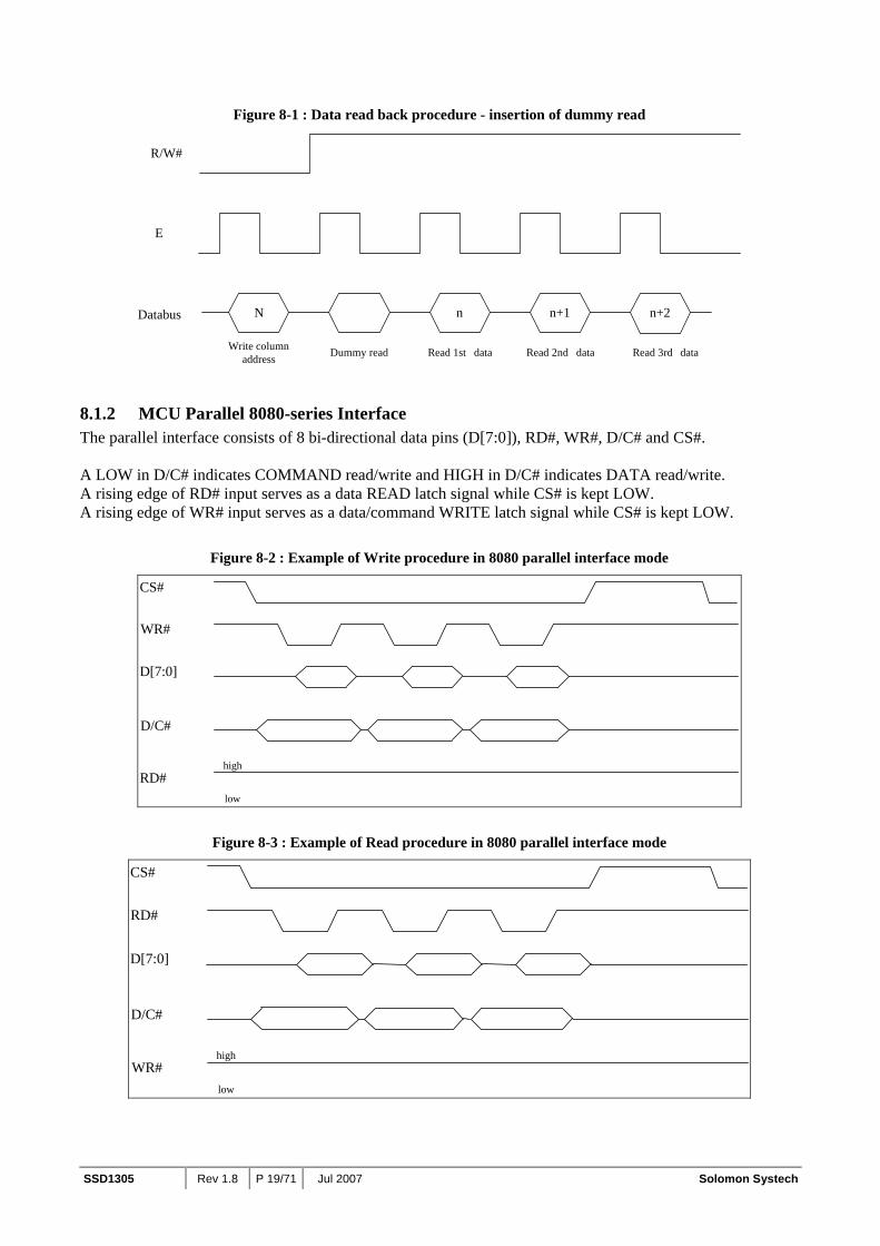
Figure 8-1 : Data read back procedure - insertion of dummy read
N n n+1 n+2
R/W#
E
Databus
Write columnaddress Read 1st dataDummy read Read 2nd data Read 3rd data
8.1.2 MCU Parallel 8080-series Interface The parallel interface consists of 8 bi-directional data pins (D[7:0]), RD#, WR#, D/C# and CS#. A LOW in D/C# indicates COMMAND read/write and HIGH in D/C# indicates DATA read/write. A rising edge of RD# input serves as a data READ latch signal while CS# is kept LOW. A rising edge of WR# input serves as a data/command WRITE latch signal while CS# is kept LOW.
Figure 8-2 : Example of Write procedure in 8080 parallel interface mode
CS#
WR#
D[7:0]
D/C#
RD#high
low
Figure 8-3 : Example of Read procedure in 8080 parallel interface mode
CS#
WR#
D[7:0]
D/C#
RD#
high
low

Solomon Systech Jul 2007 P 20/71 Rev 1.8 SSD1305
Table 8-3 : Control pins of 8080 interface (Form 1)
Function RD# WR# CS# D/C# Write command H ↑ L L Read status ↑ H L L Write data H ↑ L H Read data ↑ H L H
Note (1) ↑ stands for rising edge of signal (2) H stands for HIGH in signal (3) L stands for LOW in signal (4) Refer to Figure 13-2 for Form 1 8080-Series MPU Parallel Interface Timing Characteristics Alternatively, RD# and WR# can be keep stable while CS# serves as the data/command latch signal.
Table 8-4 : Control pins of 8080 interface (Form 2)
Function RD# WR# CS# D/C#Write command H L ↑ L Read status L H ↑ L Write data H L ↑ H Read data L H ↑ H
Note (1) ↑ stands for rising edge of signal (2) H stands for HIGH in signal (3) L stands for LOW in signal (4) Refer to Figure 13-3 for Form 2 8080-Series MPU Parallel Interface Timing Characteristics In order to match the operating frequency of display RAM with that of the microprocessor, some pipeline processing is internally performed which requires the insertion of a dummy read before the first actual display data read. This is shown in Figure 8-4.
Figure 8-4 : Display data read back procedure - insertion of dummy read
N n n+1 n+2
WR#
RD#
Databus
Write columnaddress Read 1st dataDummy read Read 2nd data Read 3rd data

SSD1305 Rev 1.8 P 21/71 Jul 2007 Solomon Systech
8.1.3 MCU Serial Interface The serial interface consists of serial clock SCLK, serial data SDIN, D/C#, CS#. In SPI mode, D0 acts as SCLK, D1 acts as SDIN. For the unused data pins, D2 should be left open. The pins from D3 to D7, E and R/W# can be connected to an external ground.
Table 8-5 : Control pins of Serial interface
Function E R/W# CS# D/C#Write command Tie LOW Tie LOW L L Write data Tie LOW Tie LOW L H
SDIN is shifted into an 8-bit shift register on every rising edge of SCLK in the order of D7, D6, ... D0. D/C# is sampled on every eighth clock and the data byte in the shift register is written to the Graphic Display Data RAM (GDDRAM) or command register in the same clock. Under serial mode, only write operations are allowed.
Figure 8-5 : Write procedure in SPI mode
8.1.4 MCU I2C Interface The I2C communication interface consists of slave address bit SA0, I2C-bus data signal SDA (SDAOUT/D2 for output and SDAIN/D1 for input) and I2C-bus clock signal SCL (D0). Both the data and clock signals must be connected to pull-up resistors. RES# is used for the initialization of device.
a) Slave address bit (SA0) SSD1305 has to recognize the slave address before transmitting or receiving any information by the I2C-bus. The device will respond to the slave address following by the slave address bit (“SA0” bit) and the read/write select bit (“R/W#” bit) with the following byte format, b7 b6 b5 b4 b3 b2 b1 b0 0 1 1 1 1 0 SA0 R/W# “SA0” bit provides an extension bit for the slave address. Either “0111100” or “0111101”, can be selected as the slave address of SSD1305. D/C# pin acts as SA0 for slave address selection. “R/W#” bit is used to determine the operation mode of the I2C-bus interface. R/W#=1, it is in read mode. R/W#=0, it is in write mode.
D7 D6 D5 D4 D3 D2 D1 D0
SCLK(D0)
SDIN(D1)
DB1 DB2 DBn
CS#
D/C#
SDIN/ SCLK

Solomon Systech Jul 2007 P 22/71 Rev 1.8 SSD1305
b) I2C-bus data signal (SDA) SDA acts as a communication channel between the transmitter and the receiver. The data and the acknowledgement are sent through the SDA. It should be noticed that the ITO track resistance and the pulled-up resistance at “SDA” pin becomes a voltage potential divider. As a result, the acknowledgement would not be possible to attain a valid logic 0 level in “SDA”. “SDAIN” and “SDAOUT” are tied together and serve as SDA. The “SDAIN” pin must be connected to act as SDA. The “SDAOUT” pin may be disconnected. When “SDAOUT” pin is disconnected, the acknowledgement signal will be ignored in the I2C-bus.
c) I2C-bus clock signal (SCL) The transmission of information in the I2C-bus is following a clock signal, SCL. Each transmission of data bit is taken place during a single clock period of SCL.
8.1.4.1 I2C-bus Write data The I2C-bus interface gives access to write data and command into the device. Please refer to Figure 8-6 for the write mode of I2C-bus in chronological order.
Figure 8-6 : I2C-bus data format
0 1 1 1 1
SA
0
P
Slave Address m ≥ 0 words n ≥ 0 bytes MSB ……………….LSB
1 byte
Write mode
SSD1305 Slave Address
R/W
#
D/C
#C
oA
CK
AC
KControl byte Data byte Control byte
AC
K Data byte
AC
K
S
0 1 1 1 1 0
SA
0 R
/W#
Co
D/C
AC
K
Control byte
Note: Co – Continuation bit D/C# – Data / Command Selection bit ACK – Acknowledgement SA0 – Slave address bit R/W# – Read / Write Selection bit S – Start Condition / P – Stop Condition
0 0 0 0 0 0
0 1 1 1 1 0
D/C
#C
oA
CK
SSD1305 Rev 1.8 P 23/71 Jul 2007 Solomon Systech
S
START condition
SDA
SCL
P
STOP condition
SDA
SCL
tHSTART tSSTOP
8.1.4.2 Write mode for I2C
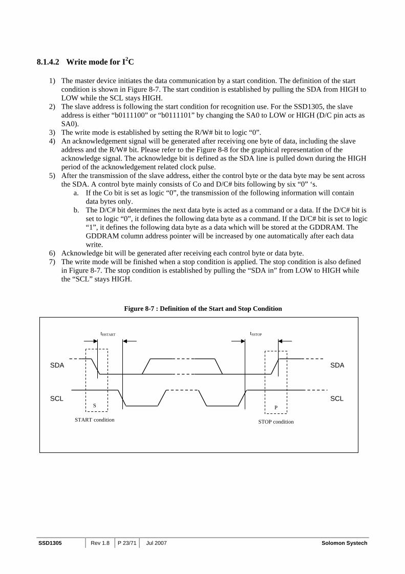
1) The master device initiates the data communication by a start condition. The definition of the start condition is shown in Figure 8-7. The start condition is established by pulling the SDA from HIGH to LOW while the SCL stays HIGH.
2) The slave address is following the start condition for recognition use. For the SSD1305, the slave address is either “b0111100” or “b0111101” by changing the SA0 to LOW or HIGH (D/C pin acts as SA0).
3) The write mode is established by setting the R/W# bit to logic “0”. 4) An acknowledgement signal will be generated after receiving one byte of data, including the slave
address and the R/W# bit. Please refer to the Figure 8-8 for the graphical representation of the acknowledge signal. The acknowledge bit is defined as the SDA line is pulled down during the HIGH period of the acknowledgement related clock pulse.
5) After the transmission of the slave address, either the control byte or the data byte may be sent across the SDA. A control byte mainly consists of Co and D/C# bits following by six “0” ‘s.
a. If the Co bit is set as logic “0”, the transmission of the following information will contain data bytes only.
b. The D/C# bit determines the next data byte is acted as a command or a data. If the D/C# bit is set to logic “0”, it defines the following data byte as a command. If the D/C# bit is set to logic “1”, it defines the following data byte as a data which will be stored at the GDDRAM. The GDDRAM column address pointer will be increased by one automatically after each data write.
6) Acknowledge bit will be generated after receiving each control byte or data byte. 7) The write mode will be finished when a stop condition is applied. The stop condition is also defined
in Figure 8-7. The stop condition is established by pulling the “SDA in” from LOW to HIGH while the “SCL” stays HIGH.
Figure 8-7 : Definition of the Start and Stop Condition

Solomon Systech Jul 2007 P 24/71 Rev 1.8 SSD1305
Figure 8-8 : Definition of the acknowledgement condition
Please be noted that the transmission of the data bit has some limitations. 1. The data bit, which is transmitted during each SCL pulse, must keep at a stable state within the “HIGH”
period of the clock pulse. Please refer to the Figure 8-9 for graphical representations. Except in start or stop conditions, the data line can be switched only when the SCL is LOW.
2. Both the data line (SDA) and the clock line (SCL) should be pulled up by external resistors.
Figure 8-9 : Definition of the data transfer condition
8.2 Command Decoder This module determines whether the input data is interpreted as data or command. Data is interpreted based upon the input of the D/C# pin. If D/C# pin is HIGH, D[7:0] is interpreted as display data written to Graphic Display Data RAM (GDDRAM). If it is LOW, the input at D[7:0] is interpreted as a command. Then data input will be decoded and written to the corresponding command register.
DATA OUTPUT BY RECEIVER
DATA OUTPUT BY TRANSMITTER
SCL FROM MASTER
S
START Condition
Clock pulse for acknowledgement
1 8 9
Non-acknowledge
2
Acknowledge
Data line is stable
SDA
SCL
Change of data

SSD1305 Rev 1.8 P 25/71 Jul 2007 Solomon Systech
8.3 Oscillator Circuit and Display Time Generator
Figure 8-10 : Oscillator Circuit and Display Time Generator
Divider
InternalOscillator
FoscMUXCL
CLK DCLK
DisplayClock
CLS
This module is an on-chip LOW power RC oscillator circuitry. The operation clock (CLK) can be generated either from internal oscillator or external source CL pin. This selection is done by CLS pin. If CLS pin is pulled HIGH, internal oscillator is chosen and CL should be left open. Pulling CLS pin LOW disables internal oscillator and external clock must be connected to CL pins for proper operation. When the internal oscillator is selected, its output frequency Fosc can be changed by command D5h A[7:4]. The display clock (DCLK) for the Display Timing Generator is derived from CLK. The division factor “D” can be programmed from 1 to 16 by command D5h
DCLK = FOSC / D The frame frequency of display is determined by the following formula.
MuxofNo.K DF
F oscFRM ××
=
where • D stands for clock divide ratio. It is set by command D5h A[3:0]. The divide ratio has the range from 1 to
16. • K is the number of display clocks per row. The value is derived by
K = Phase 1 period + Phase 2 period + BANK0 pulse width = 2 + 2 + 50 = 54 at power on reset (Please refer to Section 8.6 “Segment Drivers / Common Drivers” for the details of the “Phase”)
• Number of multiplex ratio is set by command A8h. The power on reset value is 63 (i.e. 64MUX). • FOSC is the oscillator frequency. It can be changed by command D5h A[7:4]. The higher the register
setting results in higher frequency.

Solomon Systech Jul 2007 P 26/71 Rev 1.8 SSD1305
8.4 FR synchronization FR synchronization signal can be used to prevent tearing effect.
The starting time to write a new image to OLED driver is depended on the MCU writing speed. If MCU can finish writing a frame image within one frame period, it is classified as fast write MCU. For MCU needs longer writing time to complete (more than one frame but within two frames), it is a slow write one. For fast write MCU: MCU should start to write new frame of ram data just after rising edge of FR pulse and should be finished well before the rising edge of the next FR pulse. For slow write MCU: MCU should start to write new frame ram data after the falling edge of the 1st FR pulse and must be finished before the rising edge of the 3rd FR pulse.
8.5 Reset Circuit When RES# input is LOW, the chip is initialized with the following status:
1. Display is OFF 2. 132 x 64 Display Mode 3. Normal segment and display data column address and row address mapping (SEG0 mapped to
address 00h and COM0 mapped to address 00h) 4. Shift register data clear in serial interface 5. Display start line is set at display RAM address 0 6. Column address counter is set at 0 7. Normal scan direction of the COM outputs 8. Contrast control register is set at 80h 9. Normal display mode (Equivalent to A4h command)
Fast write MCU Slow write MCU
SSD1305 displaying memory updates to OLED screen
One frame
FR
100%
0%
Memory Access Process
Time

SSD1305 Rev 1.8 P 27/71 Jul 2007 Solomon Systech
8.6 Segment Drivers / Common Drivers Segment drivers deliver 132 current sources to drive the OLED panel. The driving current can be adjusted from 0 to 320uA with 256 steps. Common drivers generate voltage-scanning pulses. The segment driving waveform is divided into three phases:
1. In phase 1, the OLED pixel charges of previous image are discharged in order to prepare for next image content display.
2. In phase 2, the OLED pixel is driven to the targeted voltage. The pixel is driven to attain the corresponding voltage level from VSS. The period of phase 2 can be programmed in length from 1 to 15 DCLKs. If the capacitance value of the pixel of OLED panel is larger, a longer period is required to charge up the capacitor to reach the desired voltage.
3. In phase 3, the OLED driver switches to use current source to drive the OLED pixels and this is the current drive stage. SSD1305 employs PWM (Pulse Width Modulation) method to control the brightness of area color A, B, C, D color individually. The longer the waveform in current drive stage is, the brighter is the pixel and vice versa.
Figure 8-11 : Segment Output Waveform in three phases
After finishing phase 3, the driver IC will go back to phase 1 to display the next row image data. This three-step cycle is run continuously to refresh image display on OLED panel. The length of phase 3 for area colors: A,B,C and monochrome BANK0 can be configured by command 91h “Set Look Up Table”. There are 64 steps available for each color but the one of color D is fixed at 64. The unit of the step is in DCLK. For example, the look up table for area color A, B, is set to 20, 40 DCLKs respectively. Color B is set to be brighter than color A. Then the result segment output waveform of these two colors is shown below.
Figure 8-12 : Segment Output Waveform for two different colors LUT setting
Segment
VSS
Phase: 1 2 3
Longer phase 3 => brighter pixel
Segment
VSS
Color A 20 DCLKs
64 DCLKs (fixed)
44 DCLKs 24 DCLKs
64 DCLKs (fixed)
Color B 40 DCLKs
Time
Time

Solomon Systech Jul 2007 P 28/71 Rev 1.8 SSD1305
In phase 3, the segment output waveforms under the monochrome mode and area color mode are different. In monochrome mode, if the length of current drive pulse width is set to 50, after finishing 50 DCLKs in current drive phase, the driver IC will go back to phase 1 for next row display.
Figure 8-13 : Example of Segment Output Waveform of monochrome display section under monochrome mode
In area color mode, the phase 3 of both BANK0 and area color banks (BANK1 to BANK32) are fixed into 64 DCLKs. For instance, if the length of the pulse width is set to 50, then after the end of 50 DCLKs of current drive phase, the segment waveform will be gone to VSS level and the driver is still in current drive phase. This phase will be end after 64 DCLKs from the start of the phase is passed. And then the drive goes back to phase 1 for next row display. Figure 8-14 shows the example of the segment output waveform of area color display section when the pulse width of area color is set to 50.
Figure 8-14 : Example of Segment Output Waveform of area color display section under area color mode
Segment
VSS
50 DCLKs
Segment
VSS
50 DCLKs
64 DCLKs (fixed)
64 DCLKs (fixed)
Time
Time

SSD1305 Rev 1.8 P 29/71 Jul 2007 Solomon Systech
8.7 Graphic Display Data RAM (GDDRAM) The GDDRAM is a bit mapped static RAM holding the bit pattern to be displayed. The size of the RAM is 132 x 64 bits and the RAM is divided into eight pages, from PAGE0 to PAGE7, as shown in Figure 8-15. In GDDRAM, PAGE0 and PAGE1 are belonged to area color section with resolution 132x16. PAGE2 to PAGE7 are used for monochrome 132x48 dot matrix display.
Figure 8-15 : GDDRAM pages structure of SSD1305
When one data byte is written into GDDRAM, all the rows image data of the same page of the current column are filled (i.e. the whole column (8 bits) pointed by the column address pointer is filled.). Data bit D0 is written into the top row, while data bit D7 is written into bottom row as shown in Figure 8-16.
Figure 8-16 : Enlargement of GDDRAM (No row re-mapping and column-remapping)
PAGE0, BANK1 PAGE0, BANK16
PAGE1, BANK17 PAGE1, BANK32
BANK0 (Background) PAGE2 – PAGE7
Row re-mapping PAGE0 (COM 63-COM56)
PAGE1 (COM 55-COM48)
PAGE2 (COM47-COM40)
PAGE3 (COM39-COM32)
PAGE4 (COM31-COM24)
PAGE5 (COM23-COM16)
PAGE6 (COM15-COM8)
PAGE7 (COM 7-COM0)
PAGE0 (COM0-COM7)
PAGE1 (COM8-COM15)
PAGE2 (COM16-COM23)
PAGE3 (COM24-COM31)
PAGE4 (COM32-COM39)
PAGE5 (COM40-COM47)
PAGE6 (COM48–COM55) PAGE7 (COM56-COM63)
SEG0 ---------------------------------------------------------------SEG131 Column re-mapping SEG131 ---------------------------------------------------------------SEG0
LSB D0
MSB D7
Each lattice represents one bit of image data
....................PAGE2
COM16COM17
: : : : :
COM23
SEG
0 SE
G1
SEG
2 SE
G3
SEG
4
SEG
127
SEG
128
SEG
129
SEG
130
SEG
131
....................

Solomon Systech Jul 2007 P 30/71 Rev 1.8 SSD1305
For mechanical flexibility, re-mapping on both Segment and Common outputs can be selected by software as shown in Figure 8-15. For vertical shifting of the display, an internal register storing the display start line can be set to control the portion of the RAM data to be mapped to the display (command D3h).
8.8 Area Color Decoder The 132x64 display matrix is divided into 8 pages. The first two pages, PAGE0 and PAGE1, are divided into 32 banks. BANK16 and BANK32 consist of a display area of 12x8 pixels. Other banks (BANK0 to BANK15 & BANK17 to BANK31) have matrices of 8x8 pixels. Each bank can be programmed to any one of the four colors (color A, B, C and D) as the example shown in Figure 8-17. Detailed operation can be referred to command 92h in Table 9-1.
Figure 8-17 : Example of area color assignment on a 132x64 OLED panel
A B C D A A A A A A A A A A D CC A B C D B B B B B B B B D A B
8
8
12
8
8
BANK1 BANK16
BANK32BANK17

SSD1305 Rev 1.8 P 31/71 Jul 2007 Solomon Systech
8.9 SEG/COM Driving block This block is used to derive the incoming power sources into the different levels of internal use voltage and current.
• VCC is the most positive voltage supply. • VCOMH is the Common deselected level. It is internally regulated. • VLSS is the ground path of the analog and panel current. • IREF is a reference current source for segment current drivers ISEG. The relationship between reference
current and segment current of a color is:
ISEG = Contrast / 256 x IREF x scale factor in which
the contrast (0~255) is set by Set Contrast command 81h; and the scale factor is 32 by default.
The magnitude of IREF is controlled by the value of resistor, which is connected between IREF pin and Vss as shown in Figure 8-18. It is recommended to set IREF to 10uA+/- 2uA so as to achieve ISEG = 320uA at maximum contrast 255.
Figure 8-18 : IREF Current Setting by Resistor Value
Since the voltage at IREF pin is VCC – 3V, the value of resistor R1 can be found as below.
R1 = (Voltage at IREF – VSS) / IREF = (VCC – 3) / 10uA ≈ 910kΩ for VCC = 12V.
SSD1305
IREF (voltage at this pin = VCC – 3)
R1
VSS
IREF ~ 10uA

Solomon Systech Jul 2007 P 32/71 Rev 1.8 SSD1305
8.10 Power ON and OFF sequence The following figures illustrate the recommended power ON and power OFF sequence of SSD1305 (assume VDD and VDDIO are at the same voltage level). Power ON sequence:
1. Power ON VDD, VDDIO. 2. After VDD, VDDIO become stable, set RES# pin LOW (logic low) for at least 3us (t1) and then HIGH
(logic high). 3. After set RES# pin LOW (logic low), wait for at least 3us (t2). Then Power ON VCC.
(1) 4. After VCC become stable, send command AFh for display ON. SEG/COM will be ON after 100ms
(tAF). Figure 8-19 : The Power ON sequence
Power OFF sequence:
1. Send command AEh for display OFF. 2. Power OFF VCC.
(1), (2) 3. Wait for tOFF. Power OFF VDD, VDDIO. .(where Minimum tOFF=0ms, Typical tOFF=100ms)
Figure 8-20 : The Power OFF sequence
Note: (1) Since an ESD protection circuit is connected between VDD, VDDIO and VCC, VCC becomes lower than VDD whenever VDD, VDDIO is ON and VCC is OFF as shown in the dotted line of VCC in Figure 8-19 and Figure 8-20. (2)
VCC should be kept float (disable) when it is OFF.
OFF VDD ,VDDIO
VDD ,VDDIO
VCC Send command AEh for display OFF OFF VCC
GND
GND tOFF
GND
ON VDD, VDDIO RES# ON VCC Send AFh command for Display ON
VDD, VDDIO
RES#
GND
t1
SEG/COM
tAF
ON OFF
VCC
GND t2

SSD1305 Rev 1.8 P 33/71 Jul 2007 Solomon Systech
8.11 DC-DC Converter This is a switching voltage generator circuit, designed for handheld applications. In the SSD1305 an internal DC-DC voltage converter accompanying an external application circuit (See Figure 8-21 below) can generate a high voltage supply, VCC, from a low voltage supply input, VDD. The VCC is the voltage supply to the OLED driver block. Below is an example application circuit for the input voltage of 2.8V VDD to generate VCC of 12V @0mA ~ 20mA application.
Figure 8-21 : DC-DC voltage converter circuit
GND
VDDB
VBREF
VSSB
GDR
FB
+
VDD
GND
+
GND
+
GND
VCC
L1 D1
Q1
R1
R2
C2
C1
C5
+
C6
+
C4
+
C3
Note (1) L1, D1, Q1, C5 should be grouped close together on PCB layout. (2) R1, R2, C1 should be grouped close together on PCB layout. (3) The VCC output voltage level can be adjusted by R1and R2, the reference formula is:
VCC = 0.8x (R1+R2) / R2 The value of (R1+R2) should be between 500k Ω. to 2MΩ.

Solomon Systech Jul 2007 P 34/71 Rev 1.8 SSD1305
Table 8-6 : Passive component selection
Components Typical Value Remark L1 Inductor, 22uH Over 0.5A current rating
Low DC resistance D1 Schottky diode MBR0530 [On Semiconductor]
0.5A Q1 MOSFET NTA4153N [On Semiconductor]
Low Rds (Drain- source resistance) Over 0.5A current rating
R1 Resistor, 1MΩ 1% R2 Resistor, 75KΩ 1% C1 Capacitor, 68nF 6V C2 Capacitor, 10uF 16V C3 Capacitor, 10nF 16V C4 Capacitor, 10nF 16V C5 Capacitor, 10uF 16V C6 Capacitor, 10nF 16V

SSD1305 Rev 1.8 P 35/71 Jul 2007 Solomon Systech
9 COMMAND TABLE
Table 9-1: Command Table
(D/C#=0, R/W#(WR#) = 0, E(RD#=1) unless specific setting is stated) Fundamental Command Table D/C# Hex D7 D6 D5 D4 D3 D2 D1 D0 Command Description 0 00~0F 0 0 0 0 X3 X2 X1 X0
Set Lower Column Start Address for Page Addressing Mode
Set the lower nibble of the column start address register for Page Addressing Mode using X[3:0] as data bits. The initial display line register is reset to 0000b after RESET.
0 10~1F 0 0 0 1 X3 X2 X1 X0
Set Higher Column Start Address for Page Addressing Mode
Set the higher nibble of the column start address register for Page Addressing Mode using X[3:0] as data bits. The initial display line register is reset to 0000b after RESET.
0 20 0 0 1 0 0 0 0 00 A[1:0] * * * * * * A1 A0
Set Memory Addressing Mode
A[1:0] = 00b, Horizontal Addressing Mode A[1:0] = 01b, Vertical Addressing Mode A[1:0] = 10b, Page Addressing Mode (RESET) A[1:0] = 11b, Invalid
0 21 0 0 1 0 0 0 0 10 A[7:0] A7 A6 A5 A4 A3 A2 A1 A00 B[7:0] B7 B6 B5 B4 B3 B2 B1 B0
Set Column Address Setup column start and end address A[7:0] : Column start address, range : 0-131d,
(RESET=0d) B[7:0]: Column end address, range : 0-131d,
(RESET =131d)
0 22 0 0 1 0 0 0 1 00 A[2:0] * * * * * A2 A1 A00 B[2:0] * * * * * B2 B1 B0
Set Page Address Setup page start and end address A[2:0] : Page start Address, range : 0-7d, (RESET =
0d) B[2:0] : Page end Address, range : 0-7d, (RESET =
7d)
0 40~7F 0 1 X5 X4 X3 X2 X1 X0
Set Display Start Line Set display RAM display start line register from 0-63 using X5X3X2X1X0. Display start line register is reset to 000000b during RESET.
0 81 1 0 0 0 0 0 0 10 A[7:0] A7 A6 A5 A4 A3 A2 A1 A0
Set Contrast Control For BANK0
Double byte command to select 1 out of 256 contrast steps. Contrast increases as the value increases. (RESET = 80h)
0 82 1 0 0 0 0 0 1 00 A[7:0] A7 A6 A5 A4 A3 A2 A1 A0
Set Brightness For Area Color Banks
Double byte command to select 1 out of 256 brightness steps. Brightness increases as the value increases. (RESET = 80h)
0 91 1 0 0 1 0 0 0 10 X[5:0] * * X5 X4 X3 X2 X1 X00 A[5:0] * * A5 A4 A3 A2 A1 A00 B[5:0] * * B5 B4 B3 B2 B1 B00 C[5:0] * * C5 C4 C3 C2 C1 C0
Set Look Up Table (LUT)
Set current drive pulse width of BANK0, Color A, B and C. BANK0: X[5:0] = 31… 63; for pulse width set to 32 ~ 64 clocks (RESET = 110001b) Color A: A[5:0] same as above (RESET = 111111b) Color B: B[5:0] same as above (RESET = 111111b) Color C: C[5:0] same as above (RESET = 111111b) Note (1) Color D pulse width is fixed at 64 clocks pulse.

Solomon Systech Jul 2007 P 36/71 Rev 1.8 SSD1305
Fundamental Command Table D/C# Hex D7 D6 D5 D4 D3 D2 D1 D0 Command Description 0 92 1 0 0 1 0 0 1 00 A[7:0] A7 A6 A5 A4 A3 A2 A1 A00 B[7:0] B7 B6 B5 B4 B3 B2 B1 B00 C[7:0] C7 C6 C5 C4 C3 C2 C1 C00 D[7:0] D7 D6 D5 D4 D3 D2 D1 D0
Set Bank Color of BANK1 to BANK16 (PAGE0)
Set the bank color of BANK1~BANK16 to any one of the 4 colors : A, B, C and D . A[1:0] : 00b, 01b, 10b, or 11b for Color = A, B, C or
D of BANK1 A[3:2] : 00b, 01b, 10b, or 11b for Color = A, B, C or
D of BANK2 : : D[5:4]: 00b, 01b, 10b, or 11b for Color = A, B, C or D
of BANK15 D[7:6]: 00b, 01b, 10b, or 11b for Color = A, B, C or D
of BANK16
0 93 1 0 0 1 0 0 1 10 A[7:0] A7 A6 A5 A4 A3 A2 A1 A00 B[7:0] B7 B6 B5 B4 B3 B2 B1 B00 C[7:0] C7 C6 C5 C4 C3 C2 C1 C00 D[7:0] D7 D6 D5 D4 D3 D2 D1 D0
Set Bank Color of BANK17~BANK32 (PAGE1)
Set the bank color of BANK17~BANK32 to any one of the 4 colors: A, B, C and D. A[1:0] : 00b, 01b, 10b, or 11b for Color = A, B, C or
D of BANK17 A[3:2] : 00b, 01b, 10b, or 1b1 for Color = A, B, C or
D of BANK18 : :
D[5:4]: 00b, 01b, 10b, or 11b for Color = A, B, C or D of BANK31
D[7:6]: 00b, 01b, 10b, or 11b for Color = A, B, C or D of BANK32
0 A0/A1 1 0 1 0 0 0 0 X0
Set Segment Re-map X[0]=0b: column address 0 is mapped to SEG0 (RESET)
X[0]=1b: column address 131 is mapped to SEG0
0 A4/A5 1 0 1 0 0 1 0 X0 Entire Display ON X0=0b: Resume to RAM content display (RESET) Output follows RAM content X0=1b: Entire display ON Output ignores RAM content
0 A6/A7 1 0 1 0 0 1 1 X0
Set Normal/Inverse Display
X[0]=0b: Normal display (RESET) 0 in RAM: OFF in display panel 1 in RAM: ON in display panel X[0]=1b: inverse display 0 in RAM: ON in display panel 1 in RAM: OFF in display panel
0 A8 1 0 1 0 1 0 0 00 A[5:0] * * A5 A4 A3 A2 A1 A0
Set Multiplex Ratio Set MUX ratio to N+1 MUX N=A[5:0] : from 16MUX to 64MUX, RESET=
111111b (i.e. 64MUX) A[5:0] from 0 to 14 are invalid entry.
0 AA 1 0 1 0 1 0 1 0
Reserved Reserved
0 AB 1 0 1 0 1 0 1 10 A[3:0] * * * * A3 A2 A1 A00 B[7:0] B7 B6 B5 B4 B3 B2 B1 B00 C[7:0] C7 C6 C5 C4 C3 C2 C1 C0
Dim mode setting A[3:0] : Reserved (set as 0000b) B [7:0] : Set contrast for BANK0, valid range 0-255d,
please refer to command 81h C [7:0] : Set brightness for color bank, valid range 0-
255d, please refer to command 82h

SSD1305 Rev 1.8 P 37/71 Jul 2007 Solomon Systech
Fundamental Command Table D/C# Hex D7 D6 D5 D4 D3 D2 D1 D0 Command Description 0 AD 1 0 1 0 1 1 0 10 A[7:0] 1 0 0 0 1 1 1 A0
Master Configuration A[0]=0b, Select external VCC supply (RESET) A[0]=1b, Select internal DC-DC voltage converter Note (1) Refer to Section 8.11 for DC-DC converter details(2) The DC-DC converter must be enabled by the following command: ADh ; Master Configuration 8Fh ; Enable internal DC-DC AFh or ACh ; Display ON
0 AC 1 0 1 0 1 1 A1 A0 AE AF
Set Display ON/OFF
ACh = Display ON in dim mode AEh = Display OFF (sleep mode) (RESET) AFh = Display ON in normal mode
0 B0~B7 1 0 1 1 0 X2 X1 X0
Set Page Start Address for Page Addressing Mode
Set GDDRAM Page Start Address (PAGE0~PAGE7) for Page Addressing Mode using X[2:0].
0 C0/C8 1 1 0 0 X3 0 0 0
Set COM Output Scan Direction
X[3]=0b: normal mode (RESET) Scan from COM0 to COM[N –1]
X[3]=1b: remapped mode. Scan from COM[N~1] to COM0
Where N is the Multiplex ratio.
0 D3 1 1 0 1 0 0 1 10 A[5:0] * * A5 A4 A3 A2 A1 A0
Set Display Offset Set vertical shift by COM from 0~63. The value is reset to 00h after RESET.
0 D5 1 1 0 1 0 1 0 1 A[7:0] A7 A6 A5 A4 A3 A2 A1 A0
Set Display Clock Divide Ratio/Oscillator Frequency
A[3:0] : Define the divide ratio (D) of the display clocks (DCLK): Divide ratio= A[3:0] + 1, RESET is 0000b (divide ratio = 1)
A[7:4] : Set the Oscillator Frequency, FOSC. Oscillator
Frequency increases with the value of A[7:4] and vice versa. RESET is 0111b
Range:0000b~1111b Frequency increases as setting value increases. Refer to section 10.1.23 for details.
0 D8 1 1 0 1 1 0 0 00 0 0 X5 X4 0 X2 0 X0
Set Area Color Mode ON/OFF & Low Power Display Mode
X[5:4]= 00b (RESET) : monochrome mode X[5:4]= 11b Area Color enable X[2]=0b and X[0]=0b: Normal power mode(RESET)X[2]=1b and X[0]=1b: Set low power display mode
0 D9 1 1 0 1 1 0 0 10 A[7:0] A7 A6 A5 A4 A3 A2 A1 A0
Set Pre-charge Period A[3:0] : Phase 1 period of up to 15 DCLK clocks (RESET=2h); 0 is invalid entry
A[7:4] : Phase 2 period of up to 15 DCLK clocks
(RESET=2h); 0 is invalid entry

Solomon Systech Jul 2007 P 38/71 Rev 1.8 SSD1305
Fundamental Command Table D/C# Hex D7 D6 D5 D4 D3 D2 D1 D0 Command Description 0 DA 1 1 0 1 1 0 1 00 0 0 X5 X4 0 0 1 0
Set COM Pins Hardware Configuration
X[4]=0b, Sequential COM pin configuration X[4]=1b(RESET), Alternative COM pin configuration X[5]=0b(RESET), Disable COM Left/Right remap X[5]=1b, Enable COM Left/Right remap Please refer to Table 10-3 for details.
0 DB 1 1 0 1 1 0 1 10 A[5:2] 0 0 A5 A4 A3 A2 0 0
Set VCOMH Deselect Level
A[5:2] Hex code
V COMH deselect level
0000b 00h ~ 0.43 x VCC 1101b 34h ~ 0.77 x VCC (RESET) 1111b 3Ch ~ 0.83 x VCC
0 E0 1 1 1 0 0 0 0 0
Enter Read Modify Write
Enter the Read Modify Write mode. Details please refer to section 10.1.28.
0 E3 1 1 1 0 0 0 1 1
NOP Command for no operation
0 EE 1 1 1 0 1 1 1 0
Exit Read Modify Write
Exit the Read Modify Write mode (Please refer to command E0h)

SSD1305 Rev 1.8 P 39/71 Jul 2007 Solomon Systech
Graphic Acceleration Command Table D/C#Hex D7 D6 D5 D4 D3 D2 D1 D0 Command Description 0 26/27 0 0 1 0 0 1 1 X0 0 A[2:0] * * * * * A2 A1 A00 B[2:0] * * * * * B2 B1 B00 C[2:0] * * * * * C2 C1 C00 D[2:0] * * * * * D2 D1 D0
Horizontal Scroll Setup
X[0]=0, Right Horizontal Scroll X[0]=1, Left Horizontal Scroll A[2:0] : Set number of column scroll offset 000b No horizontal scroll 001b Horizontal scroll by 1 column 010b Horizontal scroll by 2 columns 011b Horizontal scroll by 3 columns 100b Horizontal scroll by 4 columns Other values are invalid. B[2:0] : Define start page address
000b – PAGE0 011b – PAGE3 110b – PAGE6001b – PAGE1 100b – PAGE4 111b – PAGE7010b – PAGE2 101b – PAGE5
C[2:0] : Set time interval between each scroll step in terms of frame frequency
000b – 6 frames 100b – 3 frames 001b – 32 frames 101b – 4 frames 010b – 64 frames 110b – 2 frame 011b – 128 frames 111b – Invalid
D[2:0] : Define end page address 000b – PAGE0 011b – PAGE3 110b – PAGE6001b – PAGE1 100b – PAGE4 111b – PAGE7010b – PAGE2 101b – PAGE5
The value of D[2:0] must be larger or equal to B[2:0]
0 29/2A 0 0 1 0 1 0 X1 X00 A[2:0] * * * * * A2 A1 A00 B[2:0] * * * * * B2 B1 B00 C[2:0] * * * * * C2 C1 C00 D[2:0] * * * * * D2 D1 D00 E[5:0] * * E5 E4 E3 E2 E1 E0
Continuous Vertical and Horizontal Scroll Setup
X1X0=01b : Vertical and Right Horizontal Scroll X1X0=10b : Vertical and Left Horizontal Scroll A[2:0] : Set number of column scroll offset 000b No horizontal scroll 001b Horizontal scroll by 1 column 010b Horizontal scroll by 2 columns 011b Horizontal scroll by 3 columns 100b Horizontal scroll by 4 columns Other values are invalid. B[2:0] : Define start page address
000b – PAGE0 011b – PAGE3 110b – PAGE6001b – PAGE1 100b – PAGE4 111b – PAGE7010b – PAGE2 101b – PAGE5
C[2:0] : Set time interval between each scroll step in terms of frame frequency
000b – 6 frames 100b – 3 frames 001b – 32 frames 101b – 4 frames 010b – 64 frames 110b – 2 frame 011b – 128 frames 111b – Invalid
D[2:0] : Define end page address 000b – PAGE0 011b – PAGE3 110b – PAGE6001b – PAGE1 100b – PAGE4 111b – PAGE7010b – PAGE2 101b – PAGE5
The value of D[2:0] must be larger or equal to B[2:0] E[5:0] : Vertical scrolling offset e.g. E[5:0]= 01h refer to offset =1 row E[5:0] =3Fh refer to offset =63 rows

Solomon Systech Jul 2007 P 40/71 Rev 1.8 SSD1305
Graphic Acceleration Command Table D/C#Hex D7 D6 D5 D4 D3 D2 D1 D0 Command Description 0 2E 0 0 1 0 1 1 1 0
Deactivate scroll Stop scrolling that is configured by command 26h/27h/29h/2Ah. Note (1) After sending 2Eh command to deactivate the scrolling action, the ram data needs to be rewritten.
0 2F 0 0 1 0 1 1 1 1
Activate scroll Start scrolling that is configured by the scrolling setup commands :26h/27h/29h/2Ah with the following valid sequences: Valid command sequence 1: 26h ;2Fh. Valid command sequence 2: 27h ;2Fh. Valid command sequence 3: 29h ;2Fh. Valid command sequence 4: 2Ah ;2Fh. For example, if “26h; 2Ah; 2Fh.” commands are issued, the setting in the last scrolling setup command, i.e. 2Ah in this case, will be executed. In other words, setting in the last scrolling setup command overwrites the setting in the previous scrolling setup commands.
0 A3 1 0 1 0 0 0 1 1 0 A[5:0] * * A5 A4 A3 A2 A1 A00 B[6:0] * B6 B5 B4 B3 B2 B1 B0
Set Vertical Scroll Area
A[5:0] : Set No. of rows in top fixed area. The No. of rows in top fixed area is referenced to the top of the GDDRAM (i.e. row 0).[RESET = 0]
B[6:0] : Set No. of rows in scroll area. This is the
number of rows to be used for vertical scrolling. The scroll area starts in the first row below the top fixed area. [RESET = 64]
Note (1) A[5:0]+B[6:0] <= MUX ratio (2) B[6:0] <= MUX ratio (3a) Vertical scrolling offset (E[5:0] in 29h/2Ah) <
B[6:0] (3b) Set Display Start Line (X5X4X3X2X1X0 of
40h~7Fh) < B[6:0] (4) The last row of the scroll area shifts to the first row
of the scroll area. (5) For 64d MUX display A[5:0] = 0, B[6:0]=64 : whole area scrolls A[5:0]= 0, B[6:0] < 64 : top area scrolls A[5:0] + B[6:0] < 64 : central area scrolls A[5:0] + B[6:0] = 64 : bottom area scrolls Please refer to Figure 10-14 for details.
Note (1) “*” stands for “Don’t care”.

SSD1305 Rev 1.8 P 41/71 Jul 2007 Solomon Systech
Table 9-2 : Read Command Table
Bit Pattern Command Description D7D6D5D4D3D2D1D0
Status Register Read
D[7] : Reserve D[6] : “1” for display OFF / “0” for display OND[5] : Reserve D[4] : Reserve D[3] : Reserve D[2] : Reserve D[1] : Reserve D[0] : Reserve
Note (1) Patterns other than those given in the Command Table are prohibited to enter the chip as a command; as unexpected results can occur.
9.1 Data Read / Write To read data from the GDDRAM, select HIGH for both the R/W# (WR#) pin and the D/C# pin for 6800-series parallel mode and select LOW for the E (RD#) pin and HIGH for the D/C# pin for 8080-series parallel mode. No data read is provided in serial mode operation. In normal data read mode the GDDRAM column address pointer will be increased automatically by one after each data read. Also, a dummy read is required before the first data read. To write data to the GDDRAM, select LOW for the R/W# (WR#) pin and HIGH for the D/C# pin for both 6800-series parallel mode and 8080-series parallel mode. The serial interface mode is always in write mode. The GDDRAM column address pointer will be increased automatically by one after each data write.
Table 9-3 : Address increment table (Automatic)
D/C# R/W# (WR#) Comment Address Increment 0 0 Write Command No 0 1 Read Status No 1 0 Write Data Yes 1 1 Read Data Yes (1)
Note (1) If read-data command is issued in read-modify-write mode no address increase occurs.

Solomon Systech Jul 2007 P 42/71 Rev 1.8 SSD1305
10 COMMAND DESCRIPTIONS
10.1 Fundamental Command
10.1.1 Set Lower Column Start Address for Page Addressing Mode (00h~0Fh) This command specifies the lower nibble of the 8-bit column start address for the display data RAM under Page Addressing Mode. The column address will be incremented by each data access. Please refer to Section Table 9-1 and Section 10.1.3 for details.
10.1.2 Set Higher Column Start Address for Page Addressing Mode (10h~1Fh) This command specifies the higher nibble of the 8-bit column start address for the display data RAM under Page Addressing Mode. The column address will be incremented by each data access. Please refer to Section Table 9-1 and Section 10.1.3 for details.
10.1.3 Set Memory Addressing Mode (20h) There are 3 different memory addressing mode in SSD1305: page addressing mode, horizontal addressing mode and vertical addressing mode. This command sets the way of memory addressing into one of the above three modes. In there, “COL” means the graphic display data RAM column. Page addressing mode (A[1:0]=10xb) In page addressing mode, after the display RAM is read/written, the column address pointer is increased automatically by 1. If the column address pointer reaches column end address, the column address pointer is reset to column start address and page address pointer is not changed. Users have to set the new page and column addresses in order to access the next page RAM content The sequence of movement of the PAGE and column address point for page addressing mode is shown in Figure 10-1.
Figure 10-1 : Address Pointer Movement of Page addressing mode COL0 COL 1 ….. COL 130 COL 131
PAGE0 PAGE1
: : : : : : PAGE6 PAGE7
In normal display data RAM read or write and page addressing mode, the following steps are required to define the starting RAM access pointer location:
• Set the page start address of the target display location by command B0h to B7h. • Set the lower start column address of pointer by command 00h~0Fh. • Set the upper start column address of pointer by command 10h~1Fh.
For example, if the page address is set to B2h, lower column address is 03h and upper column address is 00h, then that means the starting column is SEG3 of PAGE2. The RAM access pointer is located as shown in Figure 10-2. The input data byte will be written into RAM position of column 3.
Figure 10-2 : Example of GDDRAM access pointer setting in Page Addressing Mode (No row and column-remapping)
LSB D0
MSB D7
Each lattice represents one bit of image data
....................PAGE2 (Starting page)
COM16COM17
: : : : :
COM23
SEG0 SEG3 (Starting column) SEG131 RAM access pointer

SSD1305 Rev 1.8 P 43/71 Jul 2007 Solomon Systech
Horizontal addressing mode (A[1:0]=00b) In horizontal addressing mode, after the display RAM is read/written, the column address pointer is increased automatically by 1. If the column address pointer reaches column end address, the column address pointer is reset to column start address and page address pointer is increased by 1. The sequence of movement of the page and column address point for horizontal addressing mode is shown in Figure 10-3. When both column and page address pointers reach the end address, the pointers are reset to column start address and page start address (Dotted line in Figure 10-3.)
Figure 10-3 : Address Pointer Movement of Horizontal addressing mode
COL0 COL 1 ….. COL 130 COL 131 PAGE0 PAGE1
: : : : : : PAGE6 PAGE7
Vertical addressing mode: (A[1:0]=01b) In vertical addressing mode, after the display RAM is read/written, the page address pointer is increased automatically by 1. If the page address pointer reaches the page end address, the page address pointer is reset to page start address and column address pointer is increased by 1. The sequence of movement of the page and column address point for vertical addressing mode is shown in Figure 10-4. When both column and page address pointers reach the end address, the pointers are reset to column start address and page start address (Dotted line in Figure 10-4.)
Figure 10-4 : Address Pointer Movement of Vertical addressing mode
COL0 COL 1 ….. COL 130 COL 131 PAGE0 ….. PAGE1 …..
: : PAGE6 ….. PAGE7 …..
In normal display data RAM read or write and horizontal / vertical addressing mode, the following steps are required to define the RAM access pointer location:
• Set the column start and end address of the target display location by command 21h. • Set the page start and end address of the target display location by command 22h.
Example is shown in Figure 10-5.
10.1.4 Set Column Address (21h) This triple byte command specifies column start address and end address of the display data RAM. This command also sets the column address pointer to column start address. This pointer is used to define the current read/write column address in graphic display data RAM. If horizontal address increment mode is enabled by command 20h, after finishing read/write one column data, it is incremented automatically to the next column address. Whenever the column address pointer finishes accessing the end column address, it is reset back to start column address and the row address is incremented to the next row.

Solomon Systech Jul 2007 P 44/71 Rev 1.8 SSD1305
10.1.5 Set Page Address (22h) This triple byte command specifies page start address and end address of the display data RAM. This command also sets the page address pointer to page start address. This pointer is used to define the current read/write page address in graphic display data RAM. If vertical address increment mode is enabled by command 20h, after finishing read/write one page data, it is incremented automatically to the next page address. Whenever the page address pointer finishes accessing the end page address, it is reset back to start page address. The figure below shows the way of column and page address pointer movement through the example: column start address is set to 2 and column end address is set to 129, page start address is set to 1 and page end address is set to 6; Horizontal address increment mode is enabled by command 20h. In this case, the graphic display data RAM column accessible range is from column 2 to column 129 and from page 1 to page 6 only. In addition, the column address pointer is set to 2 and page address pointer is set to 1. After finishing read/write one pixel of data, the column address is increased automatically by 1 to access the next RAM location for next read/write operation (solid line in Figure 10-5). Whenever the column address pointer finishes accessing the end column 129, it is reset back to column 2 and page address is automatically increased by 1 (solid line in Figure 10-5). While the end page 6 and end column 129 RAM location is accessed, the page address is reset back to 1 and the column address is reset back to 2 (dotted line in Figure 10-5). .
Figure 10-5 : Example of Column and Row Address Pointer Movement
Col 0 Col 1 Col 2 ….. ……. Col 129 Col 130 Col 131 PAGE0 PAGE1
: : PAGE6 PAGE7 :

SSD1305 Rev 1.8 P 45/71 Jul 2007 Solomon Systech
10.1.6 Set Display Start Line (40h~7Fh) This command sets the Display Start Line register to determine starting address of display RAM, by selecting a value from 0 to 63. With value equal to 0, RAM row 0 is mapped to COM0. With value equal to 1, RAM row 1 is mapped to COM0 and so on. Refer to Table 10-1 for more illustrations.
10.1.7 Set Contrast Control for BANK0 (81h) This command sets the Contrast Setting of the display. The chip has 256 contrast steps from 00h to FFh. The segment output current increases as the contrast step value increases. See Figure 10-6 below.
Figure 10-6 : Segment current vs Contrast setting
Segment current vs Contrast setting
0
50
100
150
200
250
300
350
00 0F 1F 2F 3F 4F 5F 6F 7F 8F 9F AF BF CF DF EF FFContrast setting
Current (uA)
10.1.8 Set Brightness for Area Color Banks (82h) This command sets the Brightness Setting of the display for the area color banks. The chip has 256 brightness steps from 00h to FFh. The segment output current increases as the brightness step value increases. This setting does not affect the contrast of BANK0, which is set by command 81h.
10.1.9 Set Look Up Table (LUT) (91h) The SSD1305 provides 4 color settings - Colors A, B, C and D for the bank color of BANK1 to BANK32 under the area color mode. The color intensity (or grey scale) is defined by the current drive pulse width. This pulse width setting must be stored in the Look Up Table (LUT). The pulse width of colors A, B, C is programmable from 32 to 64 DCLKs. The color D is fixed at 64 DCLKs pulse width. For the grey scale in BANK0, the pulse width is programmable from 32 to 64 DCLKs. Please refer to 91h command in Table 9-1 for details of the LUT setting. After setting the pulse widths for the color of A, B, C, D and BANK0, the next step is to define the color of each display area. Each bank can be programmable to any one of the 4 colors (A, B, C and D). The user can use 92h and 93h commands for the bank color setting. It should be notice that this is only applicable in area color mode.
Segment output current setting: Iseg = Cr/256 x IREF x scale factor Where: Cr is contrast step IREF is reference current equals 10uA Scale factor =32

Solomon Systech Jul 2007 P 46/71 Rev 1.8 SSD1305
10.1.10 Set Bank Color of BANK1 to BANK16 (PAGE0) (92h) This command maps the bank color (pulse width) of BANK1~BANK16 to any one of the 4 colors: A, B, C and D. For details of the setting, please refer to 92h command in Table 9-1.
10.1.11 Set Bank Color of BANK17 to BANK32 (PAGE0) (93h) This command maps the bank color (pulse width) of BANK17~BANK32 to any one of the 4 colors: A, B, C and D. For details of the setting, please refer to 93h command in Table 9-1.
10.1.12 Set Segment Re-map (A0h/A1h) This command changes the mapping between the display data column address and the segment driver. It allows flexibility in OLED module design. Please refer to Table 9-1. This command only affects subsequent data input. Data already stored in GDDRAM will have no changes.
10.1.13 Entire Display ON (A4h/A5h) A4h command enable display outputs according to the GDDRAM contents. If A5h command is issued, then by using A4h command, the display will resume to the GDDRAM contents. In other words, A4h command resumes the display from entire display “ON” stage. A5h command forces the entire display to be “ON”, regardless of the contents of the display data RAM.
10.1.14 Set Normal/Inverse Display (A6h/A7h) This command sets the display to be either normal or inverse. In normal display a RAM data of 1 indicates an “ON” pixel while in inverse display a RAM data of 0 indicates an “ON” pixel.
10.1.15 Set Multiplex Ratio (A8h) This command switches the default 63 multiplex mode to any multiplex ratio, ranging from 16 to 63. The output pads COM0~COM63 will be switched to the corresponding COM signal.
10.1.16 Reserved (AAh) This command is reserved.
10.1.17 Dim Mode setting (ABh) This command contains multiple bits to configure the contrast and brightness of color bank for the display in dim mode. The brightness setting of color bank can be set different to normal mode (AFh). The display can be set in dim mode through command ACh.
10.1.18 Master Configuration (ADh) This command selects the external VCC power supply or internal DC-DC voltage converter. If internal DC-DC is selected, proper external components should be connected for the generation of the VCC voltage. Refer to Section 8.11 for DC-DC converter details. If external VCC power supply is selected, external VCC power should be connected to the VCC pin. This command will be activated after issuing Set Display ON command (ACh / AFh)

SSD1305 Rev 1.8 P 47/71 Jul 2007 Solomon Systech
10.1.19 Set Display ON/OFF (ACh/AEh/AFh) These single byte commands are used to turn the OLED panel display ON or OFF. When the display is ON, the selected circuits by Set Master Configuration command will be turned ON. When the display is OFF, those circuits will be turned OFF and the segment and common output are in high impedance state. These commands set the display to one of the three states: o ACh : Dim Mode Display ON o AEh : Display OFF o AFh : Normal Brightness Display ON where the dim mode settings are controlled by command ABh.
Figure 10-7 :Transition between different modes
10.1.20 Set Page Start Address for Page Addressing Mode (B0h~B7h) This command positions the page start address from 0 to 7 in GDDRAM under Page Addressing Mode. Please refer to Table 9-1 and Section 10.1.3 for details.
10.1.21 Set COM Output Scan Direction (C0h/C8h) This command sets the scan direction of the COM output, allowing layout flexibility in the OLED module design. Additionally, the display will show once this command is issued. For example, if this command is sent during normal display then the graphic display will be vertically flipped immediately. Please refer to Table 10-3 for details.
10.1.22 Set Display Offset (D3h) This is a double byte command. The second command specifies the mapping of the display start line to one of COM0~COM63 (assuming that COM0 is the display start line then the display start line register is equal to 0). For example, to move the COM16 towards the COM0 direction by 16 lines the 6-bit data in the second byte should be given as 010000b. To move in the opposite direction by 16 lines the 6-bit data should be given by 64 – 16, so the second byte would be 100000b. The following two tables (Table 10-1, Table 10-2) show the example of setting the command C0h/C8h and D3h.
Normal mode
Dim mode Sleep mode
AFh
AEhACh
AFh
ACh
AEh

Solomon Systech Jul 2007 P 48/71 Rev 1.8 SSD1305
Table 10-1 : Example of Set Display Offset and Display Start Line with no Remap
(a) (b) (d)(c)
(e) (f) (RAM)
Set MUX ratio(A8h)COM Normal / Remapped (C0h / C8h)Display offset (D3h)Display start line (40h - 7Fh)
COM0 Row0 RAM0 Row8 RAM8 Row0 RAM8 Row0 RAM0 Row8 RAM8 Row0 RAM8COM1 Row1 RAM1 Row9 RAM9 Row1 RAM9 Row1 RAM1 Row9 RAM9 Row1 RAM9COM2 Row2 RAM2 Row10 RAM10 Row2 RAM10 Row2 RAM2 Row10 RAM10 Row2 RAM10COM3 Row3 RAM3 Row11 RAM11 Row3 RAM11 Row3 RAM3 Row11 RAM11 Row3 RAM11COM4 Row4 RAM4 Row12 RAM12 Row4 RAM12 Row4 RAM4 Row12 RAM12 Row4 RAM12COM5 Row5 RAM5 Row13 RAM13 Row5 RAM13 Row5 RAM5 Row13 RAM13 Row5 RAM13COM6 Row6 RAM6 Row14 RAM14 Row6 RAM14 Row6 RAM6 Row14 RAM14 Row6 RAM14COM7 Row7 RAM7 Row15 RAM15 Row7 RAM15 Row7 RAM7 Row15 RAM15 Row7 RAM15COM8 Row8 RAM8 Row16 RAM16 Row8 RAM16 Row8 RAM8 Row16 RAM16 Row8 RAM16COM9 Row9 RAM9 Row17 RAM17 Row9 RAM17 Row9 RAM9 Row17 RAM17 Row9 RAM17COM10 Row10 RAM10 Row18 RAM18 Row10 RAM18 Row10 RAM10 Row18 RAM18 Row10 RAM18COM11 Row11 RAM11 Row19 RAM19 Row11 RAM19 Row11 RAM11 Row19 RAM19 Row11 RAM19COM12 Row12 RAM12 Row20 RAM20 Row12 RAM20 Row12 RAM12 Row20 RAM20 Row12 RAM20COM13 Row13 RAM13 Row21 RAM21 Row13 RAM21 Row13 RAM13 Row21 RAM21 Row13 RAM21COM14 Row14 RAM14 Row22 RAM22 Row14 RAM22 Row14 RAM14 Row22 RAM22 Row14 RAM22COM15 Row15 RAM15 Row23 RAM23 Row15 RAM23 Row15 RAM15 Row23 RAM23 Row15 RAM23COM16 Row16 RAM16 Row24 RAM24 Row16 RAM24 Row16 RAM16 Row24 RAM24 Row16 RAM24COM17 Row17 RAM17 Row25 RAM25 Row17 RAM25 Row17 RAM17 Row25 RAM25 Row17 RAM25COM18 Row18 RAM18 Row26 RAM26 Row18 RAM26 Row18 RAM18 Row26 RAM26 Row18 RAM26COM19 Row19 RAM19 Row27 RAM27 Row19 RAM27 Row19 RAM19 Row27 RAM27 Row19 RAM27COM20 Row20 RAM20 Row28 RAM28 Row20 RAM28 Row20 RAM20 Row28 RAM28 Row20 RAM28COM21 Row21 RAM21 Row29 RAM29 Row21 RAM29 Row21 RAM21 Row29 RAM29 Row21 RAM29COM22 Row22 RAM22 Row30 RAM30 Row22 RAM30 Row22 RAM22 Row30 RAM30 Row22 RAM30COM23 Row23 RAM23 Row31 RAM31 Row23 RAM31 Row23 RAM23 Row31 RAM31 Row23 RAM31COM24 Row24 RAM24 Row32 RAM32 Row24 RAM32 Row24 RAM24 Row32 RAM32 Row24 RAM32COM25 Row25 RAM25 Row33 RAM33 Row25 RAM33 Row25 RAM25 Row33 RAM33 Row25 RAM33COM26 Row26 RAM26 Row34 RAM34 Row26 RAM34 Row26 RAM26 Row34 RAM34 Row26 RAM34COM27 Row27 RAM27 Row35 RAM35 Row27 RAM35 Row27 RAM27 Row35 RAM35 Row27 RAM35COM28 Row28 RAM28 Row36 RAM36 Row28 RAM36 Row28 RAM28 Row36 RAM36 Row28 RAM36COM29 Row29 RAM29 Row37 RAM37 Row29 RAM37 Row29 RAM29 Row37 RAM37 Row29 RAM37COM30 Row30 RAM30 Row38 RAM38 Row30 RAM38 Row30 RAM30 Row38 RAM38 Row30 RAM38COM31 Row31 RAM31 Row39 RAM39 Row31 RAM39 Row31 RAM31 Row39 RAM39 Row31 RAM39COM32 Row32 RAM32 Row40 RAM40 Row32 RAM40 Row32 RAM32 Row40 RAM40 Row32 RAM40COM33 Row33 RAM33 Row41 RAM41 Row33 RAM41 Row33 RAM33 Row41 RAM41 Row33 RAM41COM34 Row34 RAM34 Row42 RAM42 Row34 RAM42 Row34 RAM34 Row42 RAM42 Row34 RAM42COM35 Row35 RAM35 Row43 RAM43 Row35 RAM43 Row35 RAM35 Row43 RAM43 Row35 RAM43COM36 Row36 RAM36 Row44 RAM44 Row36 RAM44 Row36 RAM36 Row44 RAM44 Row36 RAM44COM37 Row37 RAM37 Row45 RAM45 Row37 RAM45 Row37 RAM37 Row45 RAM45 Row37 RAM45COM38 Row38 RAM38 Row46 RAM46 Row38 RAM46 Row38 RAM38 Row46 RAM46 Row38 RAM46COM39 Row39 RAM39 Row47 RAM47 Row39 RAM47 Row39 RAM39 Row47 RAM47 Row39 RAM47COM40 Row40 RAM40 Row48 RAM48 Row40 RAM48 Row40 RAM40 Row48 RAM48 Row40 RAM48COM41 Row41 RAM41 Row49 RAM49 Row41 RAM49 Row41 RAM41 Row49 RAM49 Row41 RAM49COM42 Row42 RAM42 Row50 RAM50 Row42 RAM50 Row42 RAM42 Row50 RAM50 Row42 RAM50COM43 Row43 RAM43 Row51 RAM51 Row43 RAM51 Row43 RAM43 Row51 RAM51 Row43 RAM51COM44 Row44 RAM44 Row52 RAM52 Row44 RAM52 Row44 RAM44 Row52 RAM52 Row44 RAM52COM45 Row45 RAM45 Row53 RAM53 Row45 RAM53 Row45 RAM45 Row53 RAM53 Row45 RAM53COM46 Row46 RAM46 Row54 RAM54 Row46 RAM54 Row46 RAM46 Row54 RAM54 Row46 RAM54COM47 Row47 RAM47 Row55 RAM55 Row47 RAM55 Row47 RAM47 Row55 RAM55 Row47 RAM55COM48 Row48 RAM48 Row56 RAM56 Row48 RAM56 Row48 RAM48 - - Row48 RAM56COM49 Row49 RAM49 Row57 RAM57 Row49 RAM57 Row49 RAM49 - - Row49 RAM57COM50 Row50 RAM50 Row58 RAM58 Row50 RAM58 Row50 RAM50 - - Row50 RAM58COM51 Row51 RAM51 Row59 RAM59 Row51 RAM59 Row51 RAM51 - - Row51 RAM59COM52 Row52 RAM52 Row60 RAM60 Row52 RAM60 Row52 RAM52 - - Row52 RAM60COM53 Row53 RAM53 Row61 RAM61 Row53 RAM61 Row53 RAM53 - - Row53 RAM61COM54 Row54 RAM54 Row62 RAM62 Row54 RAM62 Row54 RAM54 - - Row54 RAM62COM55 Row55 RAM55 Row63 RAM63 Row55 RAM63 Row55 RAM55 - - Row55 RAM63COM56 Row56 RAM56 Row0 RAM0 Row56 RAM0 - - Row0 RAM0 - -COM57 Row57 RAM57 Row1 RAM1 Row57 RAM1 - - Row1 RAM1 - -COM58 Row58 RAM58 Row2 RAM2 Row58 RAM2 - - Row2 RAM2 - -COM59 Row59 RAM59 Row3 RAM3 Row59 RAM3 - - Row3 RAM3 - -COM60 Row60 RAM60 Row4 RAM4 Row60 RAM4 - - Row4 RAM4 - -COM61 Row61 RAM61 Row5 RAM5 Row61 RAM5 - - Row5 RAM5 - -COM62 Row62 RAM62 Row6 RAM6 Row62 RAM6 - - Row6 RAM6 - -COM63 Row63 RAM63 Row7 RAM7 Row63 RAM7 - - Row7 RAM7 - -
Display examples
(e) (f)(a) (b) (c) (d)
0 8 00 0 8
56 56 56Normal Normal Normal
64Normal
08
Output
Hardware pin name 0
0Normal
64 64Normal
80

SSD1305 Rev 1.8 P 49/71 Jul 2007 Solomon Systech
Table 10-2 :Example of Set Display Offset and Display Start Line with Remap
(a) (b) (d)(c)
(e) (f) (g) (RAM)
Set MUX ratio(A8h)COM Normal / Remapped (C0h / C8h)Display offset (D3h)Display start line (40h - 7Fh)
COM0 Row 63 RAM63 Row 7 RAM7 Row 63 RAM7 Row 47 RAM47 - - Row 47 RAM7 - -COM1 Row 62 RAM62 Row 6 RAM6 Row 62 RAM6 Row 46 RAM46 - - Row 46 RAM6 - -COM2 Row 61 RAM61 Row 5 RAM5 Row 61 RAM5 Row 45 RAM45 - - Row 45 RAM5 - -COM3 Row 60 RAM60 Row 4 RAM4 Row 60 RAM4 Row 44 RAM44 - - Row 44 RAM4 - -COM4 Row 59 RAM59 Row 3 RAM3 Row 59 RAM3 Row 43 RAM43 - - Row 43 RAM3 - -COM5 Row 58 RAM58 Row 2 RAM2 Row 58 RAM2 Row 42 RAM42 - - Row 42 RAM2 - -COM6 Row 57 RAM57 Row 1 RAM1 Row 57 RAM1 Row 41 RAM41 - - Row 41 RAM1 - -COM7 Row 56 RAM56 Row 0 RAM0 Row 56 RAM0 Row 40 RAM40 - - Row 40 RAM0 - -COM8 Row 55 RAM55 Row 63 RAM63 Row 55 RAM63 Row 39 RAM39 Row 47 RAM47 Row 39 RAM47 Row 47 RAM63COM9 Row 54 RAM54 Row 62 RAM62 Row 54 RAM62 Row 38 RAM38 Row 46 RAM46 Row 38 RAM46 Row 46 RAM62
COM10 Row 53 RAM53 Row 61 RAM61 Row 53 RAM61 Row 37 RAM37 Row 45 RAM45 Row 37 RAM45 Row 45 RAM61COM11 Row 52 RAM52 Row 60 RAM60 Row 52 RAM60 Row 36 RAM36 Row 44 RAM44 Row 36 RAM44 Row 44 RAM60COM12 Row 51 RAM51 Row 59 RAM59 Row 51 RAM59 Row 35 RAM35 Row 43 RAM43 Row 35 RAM43 Row 43 RAM59COM13 Row 50 RAM50 Row 58 RAM58 Row 50 RAM58 Row 34 RAM34 Row 42 RAM42 Row 34 RAM42 Row 42 RAM58COM14 Row 49 RAM49 Row 57 RAM57 Row 49 RAM57 Row 33 RAM33 Row 41 RAM41 Row 33 RAM41 Row 41 RAM57COM15 Row 48 RAM48 Row 56 RAM56 Row 48 RAM56 Row 32 RAM32 Row 40 RAM40 Row 32 RAM40 Row 40 RAM56COM16 Row 47 RAM47 Row 55 RAM55 Row 47 RAM55 Row 31 RAM31 Row 39 RAM39 Row 31 RAM39 Row 39 RAM55COM17 Row 46 RAM46 Row 54 RAM54 Row 46 RAM54 Row 30 RAM30 Row 38 RAM38 Row 30 RAM38 Row 38 RAM54COM18 Row 45 RAM45 Row 53 RAM53 Row 45 RAM53 Row 29 RAM29 Row 37 RAM37 Row 29 RAM37 Row 37 RAM53COM19 Row 44 RAM44 Row 52 RAM52 Row 44 RAM52 Row 28 RAM28 Row 36 RAM36 Row 28 RAM36 Row 36 RAM52COM20 Row 43 RAM43 Row 51 RAM51 Row 43 RAM51 Row 27 RAM27 Row 35 RAM35 Row 27 RAM35 Row 35 RAM51COM21 Row 42 RAM42 Row 50 RAM50 Row 42 RAM50 Row 26 RAM26 Row 34 RAM34 Row 26 RAM34 Row 34 RAM50COM22 Row 41 RAM41 Row 49 RAM49 Row 41 RAM49 Row 25 RAM25 Row 33 RAM33 Row 25 RAM33 Row 33 RAM49COM23 Row 40 RAM40 Row 48 RAM48 Row 40 RAM48 Row 24 RAM24 Row 32 RAM32 Row 24 RAM32 Row 32 RAM48COM24 Row 39 RAM39 Row 47 RAM47 Row 39 RAM47 Row 23 RAM23 Row 31 RAM31 Row 23 RAM31 Row 31 RAM47COM25 Row 38 RAM38 Row 46 RAM46 Row 38 RAM46 Row 22 RAM22 Row 30 RAM30 Row 22 RAM30 Row 30 RAM46COM26 Row 37 RAM37 Row 45 RAM45 Row 37 RAM45 Row 21 RAM21 Row 29 RAM29 Row 21 RAM29 Row 29 RAM45COM27 Row 36 RAM36 Row 44 RAM44 Row 36 RAM44 Row 20 RAM20 Row 28 RAM28 Row 20 RAM28 Row 28 RAM44COM28 Row 35 RAM35 Row 43 RAM43 Row 35 RAM43 Row 19 RAM19 Row 27 RAM27 Row 19 RAM27 Row 27 RAM43COM29 Row 34 RAM34 Row 42 RAM42 Row 34 RAM42 Row 18 RAM18 Row 26 RAM26 Row 18 RAM26 Row 26 RAM42COM30 Row 33 RAM33 Row 41 RAM41 Row 33 RAM41 Row 17 RAM17 Row 25 RAM25 Row 17 RAM25 Row 25 RAM41COM31 Row 32 RAM32 Row 40 RAM40 Row 32 RAM40 Row 16 RAM16 Row 24 RAM24 Row 16 RAM24 Row 24 RAM40COM32 Row 31 RAM31 Row 39 RAM39 Row 31 RAM39 Row 15 RAM15 Row 23 RAM23 Row 15 RAM23 Row 23 RAM39COM33 Row 30 RAM30 Row 38 RAM38 Row 30 RAM38 Row 14 RAM14 Row 22 RAM22 Row 14 RAM22 Row 22 RAM38COM34 Row 29 RAM29 Row 37 RAM37 Row 29 RAM37 Row 13 RAM13 Row 21 RAM21 Row 13 RAM21 Row 21 RAM37COM35 Row 28 RAM28 Row 36 RAM36 Row 28 RAM36 Row 12 RAM12 Row 20 RAM20 Row 12 RAM20 Row 20 RAM36COM36 Row 27 RAM27 Row 35 RAM35 Row 27 RAM35 Row 11 RAM11 Row 19 RAM19 Row 11 RAM19 Row 19 RAM35COM37 Row 26 RAM26 Row 34 RAM34 Row 26 RAM34 Row 10 RAM10 Row 18 RAM18 Row 10 RAM18 Row 18 RAM34COM38 Row 25 RAM25 Row 33 RAM33 Row 25 RAM33 Row 9 RAM9 Row 17 RAM17 Row 9 RAM17 Row 17 RAM33COM39 Row 24 RAM24 Row 32 RAM32 Row 24 RAM32 Row 8 RAM8 Row 16 RAM16 Row 8 RAM16 Row 16 RAM32COM40 Row 23 RAM23 Row 31 RAM31 Row 23 RAM31 Row 7 RAM7 Row 15 RAM15 Row 7 RAM15 Row 15 RAM31COM41 Row 22 RAM22 Row 30 RAM30 Row 22 RAM30 Row 6 RAM6 Row 14 RAM14 Row 6 RAM14 Row 14 RAM30COM42 Row 21 RAM21 Row 29 RAM29 Row 21 RAM29 Row 5 RAM5 Row 13 RAM13 Row 5 RAM13 Row 13 RAM29COM43 Row 20 RAM20 Row 28 RAM28 Row 20 RAM28 Row 4 RAM4 Row 12 RAM12 Row 4 RAM12 Row 12 RAM28COM44 Row 19 RAM19 Row 27 RAM27 Row 19 RAM27 Row 3 RAM3 Row 11 RAM11 Row 3 RAM11 Row 11 RAM27COM45 Row 18 RAM18 Row 26 RAM26 Row 18 RAM26 Row 2 RAM2 Row 10 RAM10 Row 2 RAM10 Row 10 RAM26COM46 Row 17 RAM17 Row 25 RAM25 Row 17 RAM25 Row 1 RAM1 Row 9 RAM9 Row 1 RAM9 Row 9 RAM25COM47 Row 16 RAM16 Row 24 RAM24 Row 16 RAM24 Row 0 RAM0 Row 8 RAM8 Row 0 RAM8 Row 8 RAM24COM48 Row 15 RAM15 Row 23 RAM23 Row 15 RAM23 - - Row 7 RAM7 - - Row 7 RAM23COM49 Row 14 RAM14 Row 22 RAM22 Row 14 RAM22 - - Row 6 RAM6 - - Row 6 RAM22COM50 Row 13 RAM13 Row 21 RAM21 Row 13 RAM21 - - Row 5 RAM5 - - Row 5 RAM21COM51 Row 12 RAM12 Row 20 RAM20 Row 12 RAM20 - - Row 4 RAM4 - - Row 4 RAM20COM52 Row 11 RAM11 Row 19 RAM19 Row 11 RAM19 - - Row 3 RAM3 - - Row 3 RAM19COM53 Row 10 RAM10 Row 18 RAM18 Row 10 RAM18 - - Row 2 RAM2 - - Row 2 RAM18COM54 Row 9 RAM9 Row 17 RAM17 Row 9 RAM17 - - Row 1 RAM1 - - Row 1 RAM17COM55 Row 8 RAM8 Row 16 RAM16 Row 8 RAM16 - - Row 0 RAM0 - - Row 0 RAM16COM56 Row 7 RAM7 Row 15 RAM15 Row 7 RAM15 - - - - - - - -COM57 Row 6 RAM6 Row 14 RAM14 Row 6 RAM14 - - - - - - - -COM58 Row 5 RAM5 Row 13 RAM13 Row 5 RAM13 - - - - - - - -COM59 Row 4 RAM4 Row 12 RAM12 Row 4 RAM12 - - - - - - - -COM60 Row 3 RAM3 Row 11 RAM11 Row 3 RAM11 - - - - - - - -COM61 Row 2 RAM2 Row 10 RAM10 Row 2 RAM10 - - - - - - - -COM62 Row 1 RAM1 Row 9 RAM9 Row 1 RAM9 - - - - - - - -COM63 Row 0 RAM0 Row 8 RAM8 Row 0 RAM8 - - - - - - - -
Display examples
(e) (f) (g)(a) (b) (c) (d)
Hardw are pin name
Output64 64 64
Remap Remap Remap0 8 00 0 8
48Remap
00
48 48Remap Remap
8 00 8
48Remap
816

Solomon Systech Jul 2007 P 50/71 Rev 1.8 SSD1305
10.1.23 Set Display Clock Divide Ratio/ Oscillator Frequency (D5h) This command consists of two functions:
• Display Clock Divide Ratio (D)(A[3:0]) Set the divide ratio to generate DCLK (Display Clock) from CLK. The divide ratio is from 1 to 16, with reset value = 1. Please refer to section 8.3 for the details relationship of DCLK and CLK.
• Oscillator Frequency (A[7:4]) Program the oscillator frequency Fosc that is the source of CLK if CLS pin is pulled high. The 4-bit value results in 16 different frequency settings available as shown below. The default setting is 0111b.
Figure 10-8 : Typical Oscillator frequency adjustment by D5 command (VDD =2.8V)
Oscillator Frequency vs D5h command setting
0
100
200
300
400
500
600
0 10 20 30 40 50 60 70 80 90 A0 B0 C0 D0 E0 F0D5h setting in hex
Freq
uenc
y (k
Hz)
Note (1) There is 10% tolerance in the above frequency values
10.1.24 Set Area Color Mode ON/OFF & Low Power Display Mode (D8h) This command is used to enable area color mode. RESET is monochrome mode. The low power display mode can reduce power consumption during IC operation.
10.1.25 Set Pre-charge Period (D9h) This command is used to set the duration of the pre-charge period. The interval is counted in number of DCLK, where RESET equals 2 DCLKs.
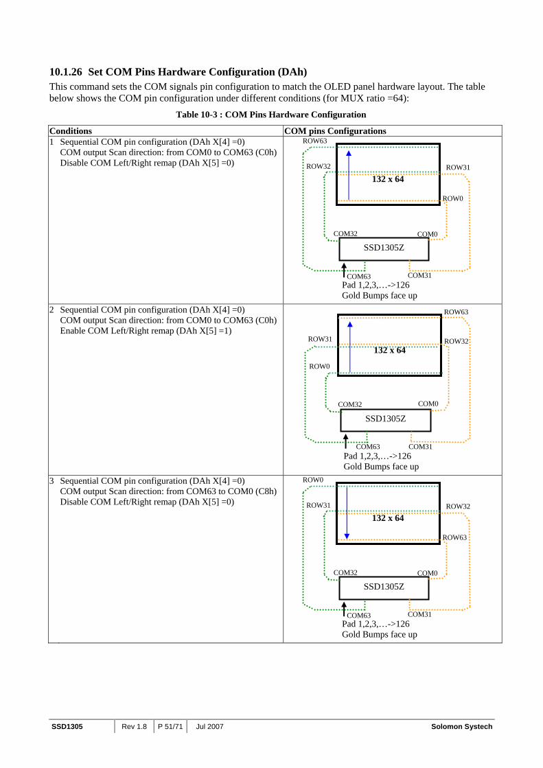
SSD1305 Rev 1.8 P 51/71 Jul 2007 Solomon Systech
10.1.26 Set COM Pins Hardware Configuration (DAh) This command sets the COM signals pin configuration to match the OLED panel hardware layout. The table below shows the COM pin configuration under different conditions (for MUX ratio =64):
Table 10-3 : COM Pins Hardware Configuration
Conditions COM pins Configurations 1 Sequential COM pin configuration (DAh X[4] =0)
COM output Scan direction: from COM0 to COM63 (C0h)Disable COM Left/Right remap (DAh X[5] =0)
2 Sequential COM pin configuration (DAh X[4] =0)
COM output Scan direction: from COM0 to COM63 (C0h)Enable COM Left/Right remap (DAh X[5] =1)
3 Sequential COM pin configuration (DAh X[4] =0)
COM output Scan direction: from COM63 to COM0 (C8h)Disable COM Left/Right remap (DAh X[5] =0)
132 x 64
ROW63
ROW32 ROW31
ROW0
Pad 1,2,3,…->126 Gold Bumps face up
SSD1305Z COM0
COM31
COM32
COM63
132 x 64 ROW32
ROW63
ROW0
ROW31
Pad 1,2,3,…->126 Gold Bumps face up
SSD1305Z
COM0
COM31 COM63
COM32
132 x 64
ROW0
ROW31 ROW32
ROW63
Pad 1,2,3,…->126 Gold Bumps face up
SSD1305Z COM0
COM31
COM32
COM63

Solomon Systech Jul 2007 P 52/71 Rev 1.8 SSD1305
Conditions COM pins Configurations 4 Sequential COM pin configuration (DAh X[4] =0)
COM output Scan direction: from COM63 to COM0 (C8h)Enable COM Left/Right remap (DAh X[5] =1)
5 Alternative COM pin configuration (DAh X[4] =1)
COM output Scan direction: from COM0 to COM63 (C0h)Disable COM Left/Right remap (DAh X[5] =0)
6 Alternative COM pin configuration (DAh X[4] =1) COM output Scan direction: from COM0 to COM63 (C0h)Enable COM Left/Right remap (DAh X[5] =1)
132 x 64
ROW0
ROW62
ROW1
ROW63
Pad 1,2,3,…->126 Gold Bumps face up
SSD1305Z COM0
COM31
COM32
COM63
ROW61
COM62
ROW2
COM1
132 x 64
ROW2
ROW63
ROW0
ROW62
Pad 1,2,3,…->126 Gold Bumps face up
SSD1305Z COM0 COM32
COM63
ROW61
COM33
ROW1
COM31
COM30
132 x 64 ROW31
ROW0
ROW63
ROW32
Pad 1,2,3,…->126 Gold Bumps face up
SSD1305Z
COM0
COM31 COM63
COM32
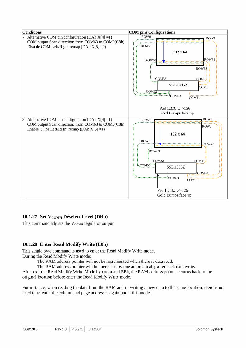
SSD1305 Rev 1.8 P 53/71 Jul 2007 Solomon Systech
Conditions COM pins Configurations 7 Alternative COM pin configuration (DAh X[4] =1)
COM output Scan direction: from COM63 to COM0(C8h) Disable COM Left/Right remap (DAh X[5] =0)
8 Alternative COM pin configuration (DAh X[4] =1)
COM output Scan direction: from COM63 to COM0(C8h) Enable COM Left/Right remap (DAh X[5] =1)
10.1.27 Set VCOMH Deselect Level (DBh) This command adjusts the VCOMH regulator output.
10.1.28 Enter Read Modify Write (E0h) This single byte command is used to enter the Read Modify Write mode. During the Read Modify Write mode:
The RAM address pointer will not be incremented when there is data read. The RAM address pointer will be increased by one automatically after each data write.
After exit the Read Modify Write Mode by command EEh, the RAM address pointer returns back to the original location before enter the Read Modify Write mode. For instance, when reading the data from the RAM and re-writing a new data to the same location, there is no need to re-enter the column and page addresses again under this mode.
132 x 64 ROW61
ROW0
ROW63
ROW1
Pad 1,2,3,…->126 Gold Bumps face up
SSD1305Z COM0 COM32
COM63
ROW2
COM33
ROW62
COM31
COM30
132 x 64
ROW63
ROW1
ROW62
ROW0
Pad 1,2,3,…->126 Gold Bumps face up
SSD1305Z COM0
COM31
COM32
COM63
ROW2
COM62
ROW61
COM1

Solomon Systech Jul 2007 P 54/71 Rev 1.8 SSD1305
Table 10-4 : Example of Read Modify Write Mode
Condition RAM & address pointer (under Horizontal addressing mode) Originally, Address Pointer point to address A
Enter Read Modify Write Mode by command E0h Data read : address pointer does not change
Data Write: address pointer increases by one automatically after each data write
Data Write: address pointer increases by one automatically after each data write
Data read : address pointer does not change
Data Write: address pointer increases by one automatically after each data write
Exit Read Modify Write Mode by command EEh Address Pointer point to address A after exit Read Modify Write Mode
10.1.29 NOP (E3h) No Operation Command
10.1.30 Exit Read Modify Write (EEh) This single byte command is used to exit the Read Modify Write mode (Please refer to Section 10.1.28. for details of the Read Modify Write Mode).
10.1.31 Status register Read This command is issued by setting D/C# ON LOW during a data read (See Figure 13-1 to Figure 13-3 for parallel interface waveform). It allows the MCU to monitor the internal status of the chip. No status read is provided for serial mode.

SSD1305 Rev 1.8 P 55/71 Jul 2007 Solomon Systech
10.2 Graphic Acceleration Command
10.2.1 Horizontal Scroll Setup (26h/27h) This command consists of 5 consecutive bytes to set up the horizontal scroll parameters and determines the scrolling start page, end page and scrolling speed. Before issuing this command the horizontal scroll must be deactivated (2Eh). Otherwise, RAM content may be corrupted. The SSD1305 horizontal scroll is designed for 132 columns scrolling. The following three figures (Figure 10-9, Figure 10-10, Figure 10-11) show the examples of using the horizontal scroll:
Figure 10-9 : Horizontal scroll example: Scroll RIGHT by 4 columns
Original Setting SEG
0
SEG
1
SEG
2
SEG
3
SEG
4
SEG
5 …
…
…
SEG
126
SEG
127
SEG
128
SEG
129
SEG
130
SEG
131
After one scroll step
SEG
128
SEG
129
SEG
130
SEG
131
SEG
0
SEG
1
…
…
…
SEG
122
SEG
123
SEG
124
SEG
125
SEG
126
SEG
127
Figure 10-10 : Horizontal scroll example: Scroll LEFT by 2 columns
Original Setting SE
G0
SEG
1
SEG
2
SEG
3
SEG
4
SEG
5 …
…
…
SEG
126
SEG
127
SEG
128
SEG
129
SEG
130
SEG
131
After one scroll step
SEG
2
SEG
3
SEG
4
SEG
5
SEG
6
SEG
7
…
…
…
SEG
128
SEG
129
SEG
130
SEG
131
SEG
0
SEG
1
Figure 10-11 : Horizontal scrolling setup example

Solomon Systech Jul 2007 P 56/71 Rev 1.8 SSD1305
10.2.2 Continuous Vertical and Horizontal Scroll Setup (29h/2Ah) This command consists of 6 consecutive bytes to set up the continuous vertical and horizontal scroll parameters and determines the scrolling start page, end page, scrolling speed and vertical scrolling offset. The bytes A[2:0], B[2:0], C[2:0] and D[2:0] of command 29h/2Ah are for the setting of the continuous horizontal scrolling. The byte E[5:0] is for the setting of the continuous vertical scrolling offset. All these bytes together are for the setting of continuous diagonal (horizontal + vertical) scrolling. If the vertical scrolling offset byte E[5:0] is set to zero, then only horizontal scrolling is performed (like command 26/27h). Alternatively, if the byte A[2:0] is set to zero and E[5:0] is not set to zero, then only vertical scrolling is performed. Before issuing this command the scroll must be deactivated (2Eh). Otherwise, RAM content may be corrupted. The following two figures (Figure 10-12 , Figure 10-13) show the examples of using the continuous vertical and horizontal scroll:
Figure 10-12 : Continuous Vertical and Horizontal scrolling setup examples

SSD1305 Rev 1.8 P 57/71 Jul 2007 Solomon Systech
Figure 10-13 : Continuous Vertical and Horizontal scrolling example: With setting in MUX ratio
As shown in Figure 10-13, the whole RAM content is displayed during scrolling regardless of the MUX ratio.
10.2.3 Deactivate Scroll (2Eh) This command stops the motion of scrolling. After sending 2Eh command to deactivate the scrolling action, the ram data needs to be rewritten.
10.2.4 Activate Scroll (2Fh) This command starts the motion of scrolling and should only be issued after the scroll setup parameters have been defined by the scrolling setup commands :26h/27h/29h/2Ah . The setting in the last scrolling setup command overwrites the setting in the previous scrolling setup commands. The following actions are prohibited after the scrolling is activated
1. RAM access (Data write or read) 2. Changing the horizontal scroll setup parameters
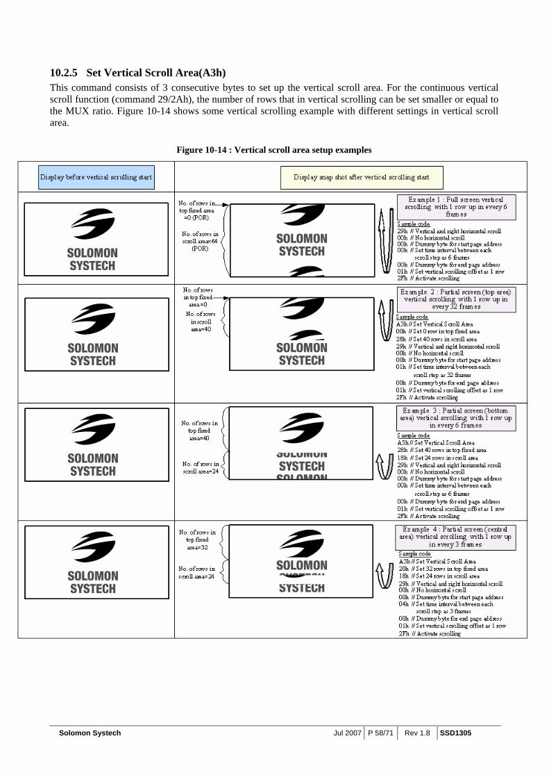
Solomon Systech Jul 2007 P 58/71 Rev 1.8 SSD1305
10.2.5 Set Vertical Scroll Area(A3h) This command consists of 3 consecutive bytes to set up the vertical scroll area. For the continuous vertical scroll function (command 29/2Ah), the number of rows that in vertical scrolling can be set smaller or equal to the MUX ratio. Figure 10-14 shows some vertical scrolling example with different settings in vertical scroll area.
Figure 10-14 : Vertical scroll area setup examples

SSD1305 Rev 1.8 P 59/71 Jul 2007 Solomon Systech
11 MAXIMUM RATINGS
Table 11-1 : Maximum Ratings (Voltage Referenced to VSS)
Symbol Parameter Value Unit VDD -0.3 to +4 V VDDIO -0.3 to VDD+0.5 V VCC
Supply Voltage 0 to 16 V
VSEG SEG output voltage 0 to VCC V VCOM COM output voltage 0 to 0.9*VCC V Vin Input voltage VSS-0.3 to VDD+0.3 V TA Operating Temperature -40 to +85 ºC Tstg Storage Temperature Range -65 to +150 ºC
Maximum ratings are those values beyond which damages to the device may occur. Functional operation should be restricted to the limits in the Electrical Characteristics tables or Pin Description section This device may be light sensitive. Caution should be taken to avoid exposure of this device to any light source during normal operation. This device is not radiation protected.

Solomon Systech Jul 2007 P 60/71 Rev 1.8 SSD1305
12 DC CHARACTERISTICS Condition (Unless otherwise specified):
Voltage referenced to VSS VDD = 2.4 to 3.5V TA = 25°C
Table 12-1 : DC Characteristics
Symbol Parameter Test Condition Min Typ Max UnitVCC Operating Voltage - 7 - 15 V VDD Logic Supply Voltage - 2.4 - 3.5 V
VDD Logic Supply Voltage (internal DC-DC enable) - 2.4 - 3.5 V
VDDIO Logic Supply Voltage for MCU interface - 1.6 - VDD V
VOH High Logic Output Level IOUT = 100uA, 3.3MHz 0.9 x VDDIO - - V VOL Low Logic Output Level IOUT = 100uA, 3.3MHz - - 0.1 x VDDIO V VIH High Logic Input Level - 0.8 x VDDIO - - V VIL Low Logic Input Level - - - 0.2 x VDDIO V ICC, SLEEP
ICC Sleep mode Current VDDIO =1.6V~3.3V, VDD = 2.4V ~3.5V, VCC = 7V~15V Display OFF, No panel attached
- - 10 uA
IDD, SLEEP
IDD Sleep mode Current VDDIO =1.6V~3.3V, VDD = 2.4V ~3.5V, VCC = 7V~15V Display OFF, No panel attached
- - 10 uA
IDDIO, SLEEP IDDIO Sleep mode Current VDDIO =1.6V~3.3V, VDD = 2.4V ~3.5V,
VCC = 7V~15V Display OFF, No panel attached
- - 10 uA
ICC
VCC Supply Current VDD = 2.7V, VCC = 12V, IREF = 10uA No loading, Display ON, All ON, DC-DC converter OFF
- 550 1000 uA
IDD
VDD Supply Current VDD = 2.7V, VCC = 12V, IREF = 10uA No loading, Display ON, All ON, DC-DC converter OFF
Contrast = FFh
- 100 300 uA
Contrast=FFh 294 320 346 Contrast=AFh - 220 - Contrast=7Fh - 159 - Contrast=3Fh - 79 -
ISEG
Segment Output Current VDD=2.7V, VCC=12V, IREF=10uA, Display ON.
Contrast=0Fh - 19 -
uA
Dev Segment output current uniformity
Dev = (ISEG – IMID)/IMID IMID = (IMAX + IMIN)/2 ISEG[0:131] = Segment current at contrast = FFh
-3 - +3 %
Adj. Dev Adjacent pin output current uniformity (contrast = FF)
Adj Dev = (I[n]-I[n+1]) / (I[n]+I[n+1]) -2 - +2 %
VCC DC-DC converter output voltage
VDD =2.8 V L2=22uH Icc = 20mA(loading)
7 - 15 V
Pwr DC-DC converter output power VDD input=2.8V, L=22uH; VCC = 15V
- - 300 mW
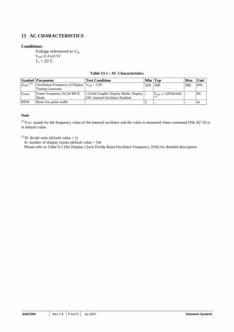
SSD1305 Rev 1.8 P 61/71 Jul 2007 Solomon Systech
13 AC CHARACTERISTICS Conditions:
Voltage referenced to VSS VDD=2.4 to3.5V TA = 25°C
Table 13-1 : AC Characteristics
Symbol Parameter Test Condition Min Typ Max UnitFOSC (1) Oscillation Frequency of Display
Timing Generator VDD = 2.8V
324 360 396 kHz
FFRM Frame Frequency for 64 MUX Mode
132x64 Graphic Display Mode, Display ON, Internal Oscillator Enabled
- FOSC x 1/(DxKx64) (2)
- Hz
RES# Reset low pulse width 3 - - us Note (1) FOSC stands for the frequency value of the internal oscillator and the value is measured when command D5h A[7:4] is in default value. (2) D: divide ratio (default value = 1) K: number of display clocks (default value = 54) Please refer to Table 9-1 (Set Display Clock Divide Ratio/Oscillator Frequency, D5h) for detailed description

Solomon Systech Jul 2007 P 62/71 Rev 1.8 SSD1305
Table 13-2 : 6800-Series MCU Parallel Interface Timing Characteristics
(VDD - VSS = 2.4V to 3.5V, VDDIO = VDD, TA = 25°C) Symbol Parameter Min Typ Max Unit tcycle Clock Cycle Time 300 - - ns
tAS Address Setup Time 0 - - ns
tAH Address Hold Time 0 - - ns
tDSW Write Data Setup Time 40 - - ns
tDHW Write Data Hold Time 7 - - ns
tDHR Read Data Hold Time 20 - - ns
tOH Output Disable Time - - 70 ns
tACC Access Time - - 140 ns
PWCSL Chip Select Low Pulse Width (read) Chip Select Low Pulse Width (write)
120 60 - - ns
PWCSH Chip Select High Pulse Width (read) Chip Select High Pulse Width (write)
60 60 - - ns
tR Rise Time - - 40 ns
tF Fall Time - - 40 ns
Figure 13-1 : 6800-series MCU parallel interface characteristics
D[7:0](WRITE)
D[7:0](READ)
E
CS#
R/W#
PWCSLtR
tF tDHW
tOH
tACC tDHR
Valid Data
tDSW
Valid Data
tcyclePWCSH
tAHtAS
D/C#

SSD1305 Rev 1.8 P 63/71 Jul 2007 Solomon Systech
Table 13-3 : 8080-Series MCU Parallel Interface Timing Characteristics
(VDD - VSS = 2.4V to 3.5V, VDDIO = VDD, TA = 25°C) Symbol Parameter Min Typ Max Unit
tcycle Clock Cycle Time 300 - - ns tAS Address Setup Time 10 - - ns tAH Address Hold Time 0 - - ns tDSW Write Data Setup Time 40 - - ns tDHW Write Data Hold Time 7 - - ns tDHR Read Data Hold Time 20 - - ns tOH Output Disable Time - - 70 ns tACC Access Time - - 140 ns tPWLR Read Low Time 120 - - ns tPWLW Write Low Time 60 - - ns tPWHR Read High Time 60 - - ns tPWHW Write High Time 60 - - ns tR Rise Time - - 40 ns tF Fall Time - - 40 ns tCS Chip select setup time 0 - - ns tCSH Chip select hold time to read signal 0 - - ns tCSF Chip select hold time 20 - - ns
Figure 13-2 : 8080-series parallel interface characteristics (Form 1)
WR#
D[7:0]
tAS
D/C#
CS#
tCS
tAH
tPWLW
tcycle
tDSW tDHW
tPWHW
tCSF
RD#
D[7:0]
tAS
D/C#
CS#
tCS
tAH
tPWLR
tcycle
tPWHR
tCSH
tACC tDHR
tOH
tF tR tF tR
Write cycle (Form 1) Read cycle (Form 1)
Figure 13-3 : 8080-series parallel interface characteristics (Form 2)
WR#
D[7:0]
D/C#
CS#
tcycle
tPWLW
tPWHW
tFtR
tCS
tAS tAH tCSF
tDSW tDHW
RD#
D[7:0]
D/C#
CS#
tcycle
tPWLR
tPWHR
tFtR
tCS
tAS tAH
tACC tDHR
tOH
tCSH
Write cycle (Form 2) Read cycle (Form 2)

Solomon Systech Jul 2007 P 64/71 Rev 1.8 SSD1305
Table 13-4 : Serial Interface Timing Characteristics
(VDD - VSS = 2.4V to 3.5V , VDDIO = VDD ,TA = 25°C) Symbol Parameter Min Typ Max Unit tcycle Clock Cycle Time 250 - - ns tAS Address Setup Time 150 - - ns tAH Address Hold Time 150 - - ns tCSS Chip Select Setup Time 120 - - ns tCSH Chip Select Hold Time 60 - - ns tDSW Write Data Setup Time 50 - - ns tDHW Write Data Hold Time 15 - - ns tCLKL Clock Low Time 100 - - ns tCLKH Clock High Time 100 - - ns tR Rise Time - - 40 ns tF Fall Time - - 40 ns
Figure 13-4 : Serial interface characteristics
t AHtAS
D/C#
Valid Data
tDHW
t CLKL
tDSW
t CLKH tcycle
t CSS tCSH
t F tR
SDIN(D 1 )
CS#
SCLK(D 0 )
D7SDIN(D1)
CS#
SCLK(D 0 )
D6 D5 D4 D3 D2 D1 D0

SSD1305 Rev 1.8 P 65/71 Jul 2007 Solomon Systech
Conditions: VDD - VSS = 2.4 to 3.5V VDDIO = VDD TA = 25°C
Table 13-5 :I2C Interface Timing Characteristics
Symbol Parameter Min Typ Max Unit
tcycle Clock Cycle Time 2.5 - - us
tHSTART Start condition Hold Time 0.6 - - us
Data Hold Time (for “SDAOUT” pin) 0 - - ns tHD
Data Hold Time (for “SDAIN” pin) 300 - - ns
tSD Data Setup Time 100 - - ns
tSSTART Start condition Setup Time (Only relevant for a repeated Start condition)
0.6 - - us
tSSTOP Stop condition Setup Time 0.6 - - us
tR Rise Time for data and clock pin - - 300 ns
tF Fall Time for data and clock pin - - 300 ns
tIDLE Idle Time before a new transmission can start 1.3 - - us
Figure 13-5 : I2C interface Timing characteristics
// //
SDA
SCL
tHSTART
tCYCLE
tHD
tR
tF tSD
tSSTART tSSTOP
tIDLE

Solomon Systech Jul 2007 P 66/71 Rev 1.8 SSD1305
The configuration for 6800-parallel interface mode, external VCC is shown in the following diagram: (VDD=2.7V, VCC =12V, IREF=10uA) Pin connected to MCU interface: D[7:0], E, R/W#, D/C#, CS#, RES# Pin internally connected to VSS: BS0, VSSB GDR, VBREF, FB should be left open if internal DC-DC converter is not used. C1: 4.7uF (1) C2: 4.7uF (1) C3: 4.7uF (1)
C4: 4.7uF (1)
R1: 910kΩ, R1= (Voltage at IREF pin-VSS)/IREF Voltage at IREF pin = VCC-3V Note (1) The capacitor value is recommended value. Select appropriate value against module application.
14 APPLICATION EXAMPLE
Figure 14-1 : Application Example of SSD1305T6R1
DISPLAY PANEL
132 x 64
CO
M62
C
OM
60
. . CO
M2
CO
M0
SEG
0 . . . . . . . . . . . . SE
G13
1 C
OM
1 C
OM
3 . . C
OM
61
CO
M63
SSD1305T6R1 BGGND VCC VCOMH IREF D[7:0] E (RD#) R/W#(W/R#) D/C# RES# CS# BS1 BS2 VDD VDDB GDR VDDIO FB VBREF VSS VCIR FR
R1
D[7:0] E (RD#) R/W# (W/R#) D/C# RES# CS# VDD VDDIO VSS
C1 C4
C2
VSS [GND]
C3
VCC

SSD1305 Rev 1.8 P 67/71 Jul 2007 Solomon Systech
15 PACKAGE INFORMATION
15.1 SSD1305Z Die Tray Information
Figure 15-1 SSD1305Z die tray information

Solomon Systech Jul 2007 P 68/71 Rev 1.8 SSD1305
15.2 SSD1305T6R1 Detail Dimension
Figure 15-2 SSD1305T6R1 Detail Dimension
SSD1
305T
6

SSD1305 Rev 1.8 P 69/71 Jul 2007 Solomon Systech

Solomon Systech Jul 2007 P 70/71 Rev 1.8 SSD1305
15.3 SSD1305T7R1 Detail Dimension
Figure 15-3 SSD1305T7R1 Detail Dimension

SSD1305 Rev 1.8 P 71/71 Jul 2007 Solomon Systech
Solomon Systech reserves the right to make changes without notice to any products herein. Solomon Systech makes no warranty, representation or guarantee regarding the suitability of its products for any particular purpose, nor does Solomon Systech assume any liability arising out of the application or use of any product or circuit, and specifically disclaims any, and all, liability, including without limitation consequential or incidental damages. “Typical” parameters can and do vary in different applications. All operating parameters, including “Typical” must be validated for each customer application by the customer’s technical experts. Solomon Systech does not con-vey any license under its patent rights nor the rights of others. Solomon Systech products are not designed, intended, or authorized for use as components in systems intended for surgical implant into the body, or other applications intended to support or sustain life, or for any other application in which the failure of the Solomon Systech product could create a situation where personal injury or death may occur. Should Buyer purchase or use Solomon Systech products for any such unintended or unauthorized application, Buyer shall indemnify and hold Solomon Systech and its offices, employees, subsidiaries, affiliates, and distributors harmless against all claims, costs, damages, and expenses, and reasonable attorney fees arising out of, directly or indirectly, any claim of personal injury or death associated with such unintended or unauthorized use, even if such claim alleges that Solomon Systech was negligent regarding the design or manufacture of the part.
All Solomon Systech Products complied with six (6) hazardous substances limitation requirement per European Union (EU) “Restriction of
Hazardous Substance (RoHS) Directive (2002/95/EC)” and China standard “电子信息产品污染控制标识要求 (SJ/T11364-2006)” with
control Marking Symbol .. Hazardous Substances test report is available upon requested.
http://www.solomon-systech.com