Embed Size (px)
Citation preview

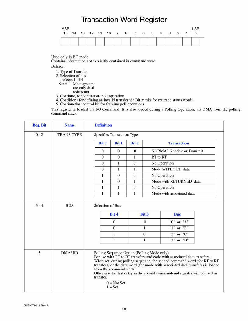
SCDCT1611 Rev A
GENERALThe CT1611 provides a complete Bus Controller and RemoteTerminal interface between the MIL-STD-1553B chip set (CT1561,CT1602, CT1610, etc.) and most microprocessor-based systems(F9450A, 68000, 8086, VME bus, Multibus, etc.). The unit isconstructed totally with CMOS technology and includes a customCMOS chip, two HC CMOS FIFO's and HCT CMOS buffers. Thusthe interface has extremly low power requirements.The CT1611 interface permits the use of all 15 mode codes and alltypes of data transfers as specified in MIL-STD-1553B in both BusController and Remote Terminal operating modes. A Remote Terminalis capable of switching to a Bus Controller when requested via theDynamic Bus Control mode code.
DATA TRANSFERSData transfers in both Bus Controller and Remote Terminal operationare performed via a DMA burst. This powerful feature insures that thehost microprocessor system will never be held up more than 16.5 usecwhen transferring 32 data words into or out of the interface. It alsoinsures that only good and complete messages will be transferred tothe host's memory. Operation of the DMA is as follows: When data isreceived from the 1553 cable via the chip set, it is loaded into aninternal FIFO at the 20 µsec/word 1553 rate. Once the completemessage has been received and has passed all validity tests, theCT1611 issues the signal DMA REQ to the subsystem. (This signalcorresponds to a HOLD request in many systems.) The hostmicroprocessor then acknowledges and grants this request by issuingthe signal DMA ACK. The CT1611 then becomes the bus master ofthe subsystem and transfers all the data on a memory-mapped basis.When the transfer is complete, the CT1611 removes its DMA REQand returns control of the microprocessor bus to the microprocessor.When data is to be transmitted on the 1553 cable, a similar DMA takesplace. Data is preloaded into the FIFO via a single DMA burst andthen transmitted.As a failsafe, an internal timeout is provided to insure that the CT1611can never control the microprocessor bus longer than 80 µsec. Inaddition, a hard-wired Master Reset input signal is provided that willplace all output signals in a tri-state condition. Therefore, in theunlikely condition of a failure in the CT1611, the host microprocessor system can never be brought down or placed in a non-recoverablestate.
A built-in test function has been included to exercise the DMAoperation and verify the message data path. This function is initiatedby an I/O command from the subsystem.
I/O CONTROLThe CT1611 can be addressed, written to, read from, and programmedmuch like any peripheral device located on a microprocessor bus. Theaddress lines and a device select input signal allow the subsystem toread or write to the CT1611 as if it were memory. In view of the factthat microprocessors are becoming very fast, two types of handshakesignals were incorporated into the CT1611, either of which may beused to permit asynchronous read and write operations. Handshakingdirectly with the 9450A, 8085, 8086 and the 6802 is the active highReady signal. Handshaking directly with the 68000 or VME andMultibus busses is the active low Acknowledge signal.
INTERFACINGTo accomodate both 8 and 16 bit microprocessor data busses, theCT1611 data path is pin programmable for either operation. Whenoperating in 8 bit mode, data is DMA'd in 8 bit bytes and thereforerequires twice the time to be transferred.Bus control signals are pin programmable for either individual readand write strobes or a common read/write signal and data strobe.Individual read and write strobes are used with the Intel 8085, 8086and Multibus. A common read/write signal and data strobe are usedwith the 9450A, 6802, 68000 and VME bus. Two separate pins areprovided for input and output data strobes. These signals may beconnected or kept separate to insure that 1553 data can never bewritten into a protected area of memory.
RTU OPERATIONThe CT1611 is powered-up and reset as a Remote Terminal. Inaddition, in Bus Controller mode, it can be changed into a RemoteTerminal via an I/O command.In Remote Terminal mode, the CT1611 uses dedicated registers for thereceived command word, the sync data word, and the vector word. Thecommand word register contains a second tier so that receivecommand words are double buffered. This feature maximizes theallowable I/O access time.Four interrupts are provided to alert the subsystem that a validmessage has been received or transmitted or that a mode command has
CT1611 Microprocessor InterfaceStandard Products
DMA Controller with Buffer Memory,
September 16, 2003www.aeroflex.comMIL-STD-1750A Compatible
FEATURES Full Bus Control and RTU Operation
Low Software Overhead
Complete BI-Directional Message Buffer
Memory-Mapped DMA Message Transfers
Simple Programmable Polling Operation in Bus Controller Mode
Pin Programmable for both 8 and 16 Bit Microprocessors
Monolithic construction using linear ASICs
Processed and screened to MIL-STD-883 specs
Aeroflex is a Class H & K MIL-PRF-38534 Manufacturer
MIL-PRF-38534 Compliant Devices Available
2SCDCT1611 Rev A
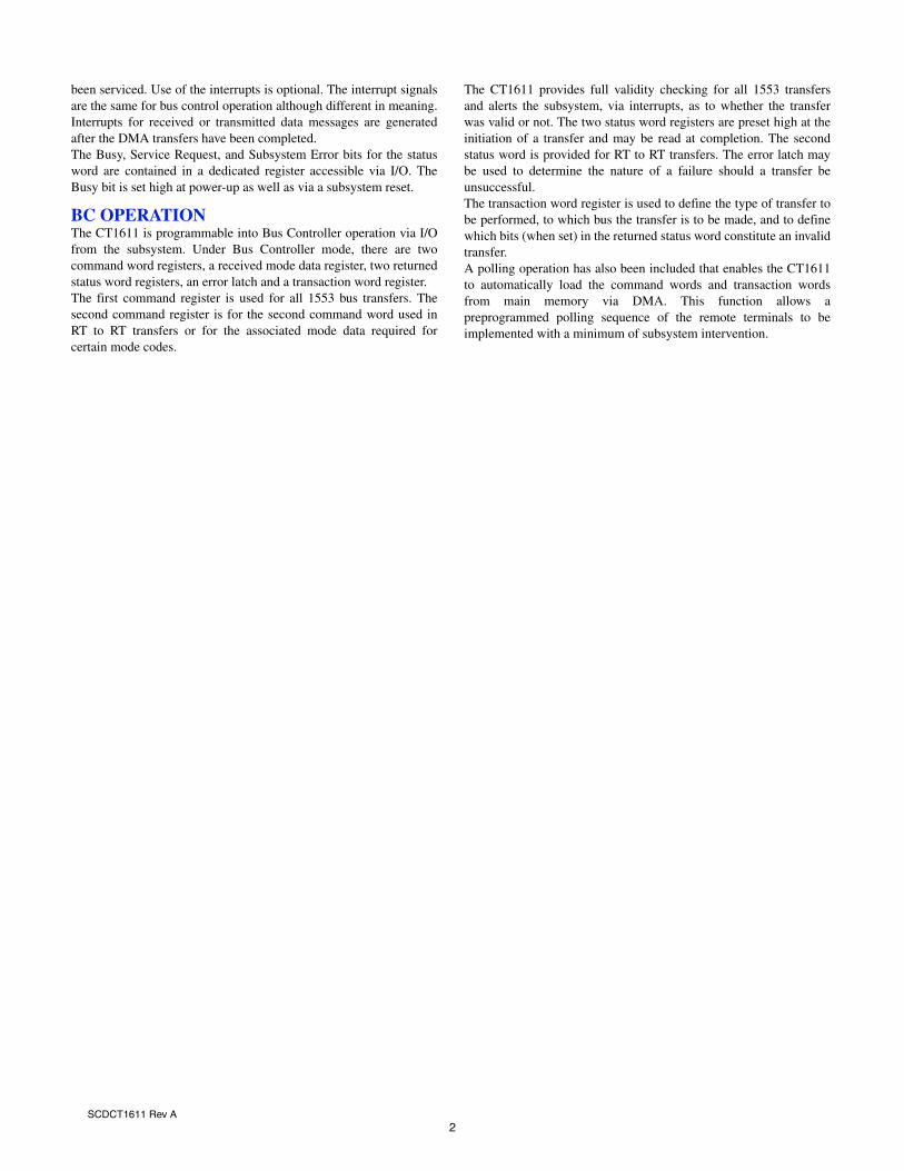
been serviced. Use of the interrupts is optional. The interrupt signalsare the same for bus control operation although different in meaning.Interrupts for received or transmitted data messages are generatedafter the DMA transfers have been completed. The Busy, Service Request, and Subsystem Error bits for the statusword are contained in a dedicated register accessible via I/O. TheBusy bit is set high at power-up as well as via a subsystem reset.
BC OPERATIONThe CT1611 is programmable into Bus Controller operation via I/Ofrom the subsystem. Under Bus Controller mode, there are twocommand word registers, a received mode data register, two returnedstatus word registers, an error latch and a transaction word register.The first command register is used for all 1553 bus transfers. Thesecond command register is for the second command word used inRT to RT transfers or for the associated mode data required forcertain mode codes.
The CT1611 provides full validity checking for all 1553 transfersand alerts the subsystem, via interrupts, as to whether the transferwas valid or not. The two status word registers are preset high at theinitiation of a transfer and may be read at completion. The secondstatus word is provided for RT to RT transfers. The error latch maybe used to determine the nature of a failure should a transfer beunsuccessful.The transaction word register is used to define the type of transfer tobe performed, to which bus the transfer is to be made, and to definewhich bits (when set) in the returned status word constitute an invalidtransfer.A polling operation has also been included that enables the CT1611to automatically load the command words and transaction wordsfrom main memory via DMA. This function allows apreprogrammed polling sequence of the remote terminals to beimplemented with a minimum of subsystem intervention.
3SCDCT1611 Rev A
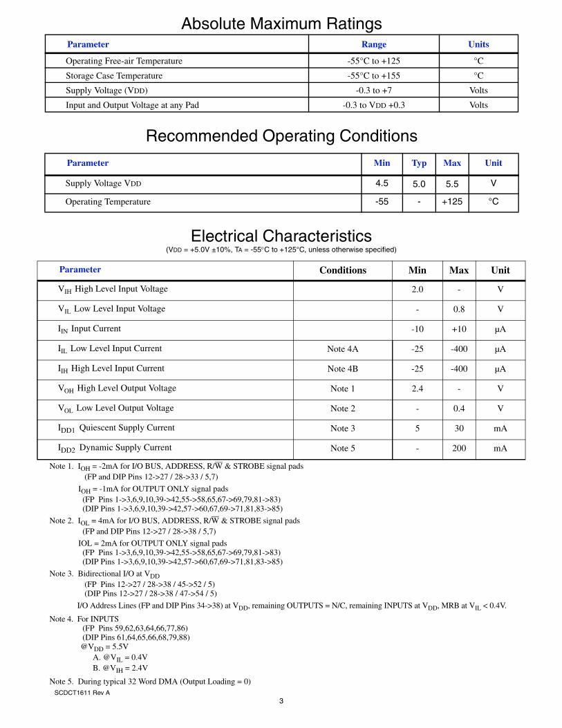
Absolute Maximum RatingsParameter Range Units
Operating Free-air Temperature -55°C to +125 °C
Storage Case Temperature -55°C to +155 °C
Supply Voltage (VDD) -0.3 to +7 Volts
Input and Output Voltage at any Pad -0.3 to VDD +0.3 Volts
Recommended Operating Conditions
Parameter Min Typ Max Unit
Supply Voltage VDD 4.5 5.0 5.5 V
Operating Temperature -55 - +125 °C
Electrical Characteristics(VDD = +5.0V ±10%, TA = -55°C to +125°C, unless otherwise specified)
Parameter Conditions Min Max Unit
VIH High Level Input Voltage 2.0 - V
VIL Low Level Input Voltage - 0.8 V
IIN Input Current -10 +10 µA
IIL Low Level Input Current Note 4A -25 -400 µA
IIH High Level Input Current Note 4B -25 -400 µA
VOH High Level Output Voltage Note 1 2.4 - V
VOL Low Level Output Voltage Note 2 - 0.4 V
IDD1 Quiescent Supply Current Note 3 5 30 mA
IDD2 Dynamic Supply Current Note 5 - 200 mA
Note 1. IOH = -2mA for I/O BUS, ADDRESS, R/W & STROBE signal pads (FP and DIP Pins 12->27 / 28->33 / 5,7)
IOH = -1mA for OUTPUT ONLY signal pads (FP Pins 1->3,6,9,10,39->42,55->58,65,67->69,79,81->83) (DIP Pins 1->3,6,9,10,39->42,57->60,67,69->71,81,83->85)
Note 2. IOL = 4mA for I/O BUS, ADDRESS, R/W & STROBE signal pads (FP and DIP Pins 12->27 / 28->38 / 5,7)
IOL = 2mA for OUTPUT ONLY signal pads (FP Pins 1->3,6,9,10,39->42,55->58,65,67->69,79,81->83) (DIP Pins 1->3,6,9,10,39->42,57->60,67,69->71,81,83->85)
Note 3. Bidirectional I/O at VDD (FP Pins 12->27 / 28->38 / 45->52 / 5) (DIP Pins 12->27 / 28->38 / 47->54 / 5)
I/O Address Lines (FP and DIP Pins 34->38) at VDD, remaining OUTPUTS = N/C, remaining INPUTS at VDD, MRB at VIL < 0.4V.
Note 4. For INPUTS (FP Pins 59,62,63,64,66,77,86) (DIP Pins 61,64,65,66,68,79,88) @VDD = 5.5V A. @VIL = 0.4V B. @VIH = 2.4V
Note 5. During typical 32 Word DMA (Output Loading = 0)

4SCDCT1611 Rev A
DMA
BIDIRECTIONAL32 WORD
DATA BUFFERFIFO
8 OR 16 BITSUBSYSTEMDATA BUS
ADDRESSANDCONTROLSIGNALS
INTERRUPTS
0
1
2
3
16 B
IT IN
TE
RN
AL
DA
TA
BU
S
TO SUBSYSTEMTO PROTOCOL HYBRID
IH
8 B
IT IN
TE
RN
AL
HIG
HW
AY
(REGISTERS)00
02
0C
0A
36
38
3C
3A
32
0E
34
BC CW1
TRANSACTION WD
OPERATION WD
RTU RCV CW
ERROR
POLL TRANS OFFSET
LAST POLL TRANS ADD
BC CW2 / AMD / VEC
RTU CW
STAT WD1
STAT WD2 / RMD / SYNC
I/ODECODER
DMACONTROLLER
BIDIRECTIONALI/O DATABUFFER
INTERRUPTGENERATOR
BUSCONTROLLERSEQUENCER
WATCH DOGDMA
TIMER
HANDSHAKEAND
CONTROL
CT1611 FUNCTIONAL BLOCK DIAGRAM
⎫
⎭⎬

5SCDCT1611 Rev A
654 7 8
1 2 3
10 11 2120
37
1216
2231
654 7 8
1 2 3
1 2 3029
6.8µ
F
T1
T2
+
+
0.01
µF
6.8µ
F
0.01
µF
142527 172015635368534
2332
1928
2433
4 9 13 18
DAT
A
DAT
A
Bus
"A
"S
tub
Cou
plin
g
+5V
2KΩ
2KΩ
T1
- T
2 ar
eTe
chni
trol
X-1
296-
1or
T-1
553-
2
**
(See
Not
e 4)
Driv
er/R
ecei
ver
Pin
out
s sh
own
are
for
CT
1487
D a
nd C
T14
87D
FA
ll S
erie
s C
T14
87, C
T15
89, C
T32
31
and
CT
3232
are
fully
com
pata
ble
(71)
69
(56)
54
(57)
55
(72)
70
(73)
71
(70)
68
(67)
65
(58)
66
(1)
1
(45)
(46)
(90)
88
(48)
46
(49)
47
(50)
48
(51)
49
(52)
50
(47)
45
(61)
59
(66)
64
(75)73
(63)61
(64)62
(62)60
(80)78
RTA
D 0
RTA
D 1
RTA
D 2
RTA
D 3
RTA
D 4
RTA
DPA
R
Term
inal
Add
ress
+ P
arity
(O
DD
)
***
MIL
-PR
F-1
553B
Chi
p S
et
Use
(X
X)
Num
bers
CT
1610
, CT
1612
, and
CT
1560
Thr
u C
T15
63ar
e fu
lly c
ompa
tabi
le
Test
Poi
nts
(May
be
used
)
(62)60
(64)62
(63)61
(80)78
(66)64
(86)
84
6 (6
9)7
(7)
8 (8
)9
(9)
2 (2
)82
(84
)83
(85
)86
(88
)87
(89
)84
(86
)3
(3)
4 (4
)5
(5)
14 (
14)
15 (
15)
76 (
78)
74 (
76)
85 (
87)
81 (
83)
80 (
82)
79 (
81)
10 (
10)
11 (
11)
12 (
12)
72 (
74)
13 (
13)
19 (
19)
20 (
20)
21 (
21)
16 (
16)
23 (
23)
18 (
18)
25 (
25)
26 (
26)
28 (
28)
27 (
27)
57 (
59)
32 (
32)
31 (
31)
34 (
34)
36 (
36)
37 (
37)
38 (
38)
39 (
39)
40 (
40)
41 (
41)
42 (
42)
43 (
43)
44 (
44)
(47)
45
(48)
46
(49)
47
(50)
48
(51)
49
(52)
50
(53)
51
(54)
52
(55)
53
(56)
54
(58)
56
(57)
55
(59)
57
(67)
65
(65)
63
(63)
66
(69)
67
(76)
74
(70)
68
(78)
76
(73)
71
(74)
72
(75)
73
(77)
75
(79)
77
(83)
81
(84)
82
(85)
83
(87)
85
(88)
86
(89)
87
(1)
1
(81)
79
(46)
(45)
(71)
69
(82)
80
(72)
79
(79)
77
(65)
63
(58)
56
(55)
53
(54)
52
(53)
51
(24)
24
(17)
17
(22)
22
(30)
30
(29)
29
(77)
75
(60)
58
67 (
69)
33 (
33)
58 (
60)
88 (
90)
44 (
44)
SS
ER
RS
YN
C
43 (
43)
59 (
61)
2 (2
)
3 (3
)
4 (4
)
5 (5
)
39 (
39)
40 (
40)
41 (
41)
42 (
42)
10 (
10)
11 (
11)
5 (5
)
6 (6
)
7 (7
)
8 (8
)38
(38
)37
(37
)
36 (
36)
35 (
35)
34 (
34)
33 (
33)
32 (
32)
31 (
31)
30 (
30)
29 (
29)
28 (
28)
27 (
27)
26 (
26)
25 (
25)
24 (
24)
23 (
23)
22 (
22)
21 (
21)
20 (
20)
19 (
19)
18 (
18)
17 (
17)
16 (
16)
5 (5
)
14 (
14)
13 (
13)
12 (
12)
+5V
RE
SE
TD
BR
EQ
* Ty
pica
l
Pin
ou
ts
show
n fo
r S
pect
rum
Tech
nolo
gy S
erie
s 71
11 T
TL
5/8"
20
lead
fla
t-pa
ck.
Pos
sibl
eal
tern
ate,
Q-T
EC
H S
erie
s Q
T21
TT
L 5/
8" 2
0 le
ad f
lat-
pack
(N
otto
tally
pi
n co
mpa
tabl
e w
ithS
pect
rum
Tec
nolo
gy).
.1µF
Opt
iona
l di
scre
te
outp
ut
indi
catin
gR
.T.U
. has
acc
epte
d R
ES
ET
mod
e co
deO
ptio
nal d
iscr
ete
outp
ut in
dica
ting
R.T
.U.
has
acce
pted
Dyn
amic
Bus
Con
trol
req
uest
.
+10
µF.0
1µF
.1µF
.1µF
+5V
GN
D
+15
V
-15V
+5V
+15
V
-15V
+5V
+5V
11
20 10
8
Opt
ical
dis
cret
e in
put
Opt
ical
dis
cret
e O
utpu
t
1Ω
.1µF
TB
DµF
1Ω
.1µF
TB
DµF
+5V
+5V
RTA
DE
RT
XTO
MA
NE
RPA
RE
RLT
FAIL
HS
FAIL
ER
RO
R
Test
Poi
nts
(May
be
used
)
Sub
syst
emC
ontr
ol, H
ands
hake
and
In
terr
upt L
ines
Sub
syst
emI/O
Add
ress
(10
Line
s)
Sub
syst
emI/O
Add
ress
(16
Line
s)
"Har
dwire
d" r
eset
from
Sys
tem
(i.e
. pow
er o
n r
eset
) or
AC
net
wor
k⎤ ⎦ X-1
269-
1 &
T15
53-2
are
iden
tical
, exc
ept T
-155
3-2
5. In
terr
upt F
unct
ions
:S
IGN
AL
BC
Mod
eR
TU
Mod
e
INT
R 0
INT
R 1
INT
R 2
INT
R 3
Goo
d X
fer
Inva
lid X
fer
Pol
l Op
Cm
plt
-
Val
id M
sg r
cv’d
Syn
c w
/Dat
aS
ync
(w/o
Dat
a), R
eset
, DB
CM
sg x
mt’d
, vec
tor
wd
6. A
CK
, RD
YD
are
han
dsha
ke s
igna
ls u
sed
inas
ynch
rono
us I/
O D
ata
tran
sfer
s. E
ither
sig
nal
may
be
used
dep
endi
ng o
n sy
stem
req
uire
men
ts.
7. D
MA
DAT
A A
CK
may
be
used
to e
xten
d th
e da
tatr
ansf
er ti
me
durin
g D
MA
.8.
Pin
69
defin
es µ
P in
terf
ace,
i.e
R/W
, & S
TR
BD
or
AD
ST
B &
WR
TS
TB
. (P
ins
7 &
8 m
ust b
e tie
d
DU
AL
Red
unda
nt B
C/R
TU
1553
B T
o µP
Inte
rfac
e
RTA
D P
AR
RTA
D 4
RTA
D 3
RTA
D 2
RTA
D 1
RTA
D 0
NC
NC
NC
NC
Rx
DAT
A 1
ER
RO
R
Tx
INH
1
Rx
DAT
A 1
RTA
DE
RT
XTO
MA
NE
RPA
RE
RLT
FAIL
MS
FAIL
IH71
5
IH61
4
IH51
3
IH41
2
IH31
1
IH21
0
IH19
IH08
IHE
N
IHD
IR
RE
QB
US
B
RE
QB
US
A
RT
0
BC
OP
ST
B
BC
OP
B
BC
OP
A
DTA
CK
DT
RQ
IUS
TB
SY
NC
NB
GT
VE
CTE
N/D
WE
N
EO
T
SE
RV
RF
Q
INC
MD
STA
TE
N/S
TAT
ST
B
H/L
GB
R
LST
CM
D/C
WE
N
BIT
EN
/RM
DS
TB
BU
SY
SS
ER
A
DB
AC
CC
WC
4C
WC
3C
WC
2C
WC
1C
WC
0W
C4
WC
3W
C2
WC
1W
C0
SA
4S
A3
RT
/BC
SA
2S
A1
SA
0
Tx D
ATA
Tx D
ATA
Rx
DAT
A 0
Tx
INH
0
INC
LK (
2 M
Hz
Clo
ck)
ND
RQ
Tx
/Rx
CM
SY
NC
+5V
IN
CT1
602
MIL
-PR
F-15
53B
Rx
DAT
A 0
BU
FIN
H
BC
ST
EN
0B
CS
TE
N 1
VALD
DW
SY
NC
DB
RE
QR
ES
ET
PAS
MO
N
GN
D/C
AS
E6
MH
z
Chi
pset
***
IH71
5
IH61
4
IH51
3
IH41
2
IH31
1
IH21
0
IH19
IH08
IHE
N
IHD
IR
RE
QB
US
B
RE
QB
US
A
RT
0
BC
OP
STB
BC
OP
B
BC
OP
A
DTA
CK
DT
RQ
IUS
TB
SY
NC
NB
GT
VE
CTE
N/D
WE
N
EO
T
SE
RV
RF
Q
INC
MD
STA
TE
N/S
TATS
TB
H/L
GB
R
LST
CM
D/C
WE
N
BIT
EN
/RM
DS
TB
BU
SY
SS
ER
A
DB
AC
C
CT1
611
DM
A C
on
tro
ller
µP
roce
sso
r In
terf
ace
wit
h F
IFO
Inte
rrup
tO
utpu
ts
RTA
DE
RTX
TOM
AN
ER
PAR
ER
HS
FAIL
LTFA
IL
(LS
B)
D0
D1
D2
D3
D4
D5
D6
D7
D8
D9
D10
D11
D12
D13
D14
(MS
B)
D15
(LS
B)
A0
A1
A2
A3
A4
A5
A6
A7
A8
(MS
B)
A9
NC
(A10
, 8 B
it M
ode
only
)
(ST
RB
D/W
RS
TB)
ST
RB
DI
ST
RB
DO
OU
T(S
TR
BD
/WR
STB
)IN
RD
YD
R/W
(R/W
, RD
ST
B)
DM
AR
EQ
DM
AA
CK
INT
2
INT
0
INT
1
INT
3
AC
K
DE
VIC
ES
EL
TRA
NS
MIT
/RE
CE
IVE
MA
ST
ER
RE
SE
TD
MA
DAT
AA
CK
PO
LL/D
ATA
CO
MM
ON
/CA
SE
+5V
IN6
MH
zR
T/B
C
16/B
MO
DE
0/M
OD
E1
NC
NC
NC
NC
NC
NC
Rx
DAT
A IN
2
Tx
DAT
A O
UT
2
Tx
DAT
A O
UT
2
Rx
DAT
A IN
2
Rx
DAT
A IN
1
Tx
DAT
A O
UT
1
Tx
DAT
A O
UT
1
Rx
DAT
A IN
1
GN
DG
ND
GN
DG
ND
GN
DG
ND
Rx
DAT
A O
UT
2
Rx
DAT
A IN
2
Tx
INH
IBIT
2
Tx
DAT
A IN
2
Tx
DAT
A IN
2
ST
RO
BE
2
ST
RO
BE
1
Tx
DAT
A IN
1
Tx
DAT
A IN
1
Rx
DAT
A O
UT
1
Rx
DAT
A O
UT
1
Tx
INH
IBIT
1
CT-
1487
D a
nd D
FD
ual D
rive
r/R
ecei
ver
**
(1)
(2)
(1)
(2)
(2)
(1)
+15V
+15V
+5V
+5V
-15V
-15V
DAT
A
DAT
A
Bus
"B
"S
tub
Cou
plin
g
NO
TE
S:
1. X
X P
in n
umbe
rs a
re fo
r fla
t pac
ks
2. (
XX
) P
in n
umbe
rs a
re fo
r pl
ug in
pac
kage
3. P
in n
umbe
rs fo
r C
T14
87D
(P
lug
in)
and
CT
1487
DF
(fla
t pac
k) a
re th
e sa
me.
4. P
in n
umbe
rs fo
r T
1 &
T2
in D
IP
& F
lat P
ack
pack
age
are
the
sam
e.X
-126
9-1
(DIP
)X
-126
9-1F
P (
Fla
t Pac
k)T-
1553
-2 (
DIP
)T-
1553
-2F
P (
Fla
t Pac
k)
CT
1608
FP
& C
T16
11F
P.
CT
1608
& C
T16
11.
has
guar
ante
ed -
55°C
Inpu
t Im
peda
nce
23KΩ
per
MIL
-ST
D-1
553B
.
toge
ther
)
VC
C
6MH
zO
scill
ato
rG
ND
/Cas
eOut
*
CT
1611
Ty
pica
l App
licat
ion
14
7
⎤⎦
Test
Poi
nts
(May
be
Use
d)

6SCDCT1611 Rev A
CT 1611
User’s Guide

7SCDCT1611 Rev A
10010 111010 0001118 0 29 3
Receive Command Register
WordCount
Sub-Address
RTAddress
CW DW1 DW2 DW3 SW
SubsystemAddress
MemoryData
11101
11101
11101
XXX
XXX
XXX 00010
00001
00000
DW1
DW2
DW3
SubsystemAddress
29
Continuousword count
address selector
MSB’sdetermined by
subsystem
Example of DMA Data Transfer
Transfer = 3-Word Receive Message in RTU Mode
T/R

8SCDCT1611 Rev A
TRISTATE TRISTATE
TRISTATE TRISTATE
Tristate with Pullup
200ns to 400ns
60ns MAX (Note 1)
100ns MAX
DATA Latched
180ns to 375ns 65ns MAX
Tristate with Pullup
R / W
ADDRESS
DEVICE SELECT
STRBD
RDYD
DATA
ACK
(From UP System)
(From UP System)
(From UP System)
(From UP System)
(From DMA Controller)
(From DMA Controller)
(From up System)
ADDRESS VALID
VALID
I / O WRITE OPERATION
Notes:1. Measured from STRBD or DEVICE SELECT whichever is valid LAST.RDYD requires the coincidence of STRBD and DEVICE SELECT.
TRISTATE TRISTATE
TRISTATE
Tristate with Pullup
200ns to 400ns
60ns MAX (Note 1)
100ns MAX
180ns to 375ns
65ns MAX
Tristate with Pullup
R / W
ADDRESS
DEVICE SELECT
STRBD
RDYD
DATA
ACK
(From UP System)
(From UP System)
(From UP System)
(From DMA Controller)
(From DMA Controller)
(From DMA Controller)
(From up System)
I / O READ OPERATION
Notes:1. Requires BOTH STRBD or DEVICE SELECT to be LOW.2. DATA will be valid 100ns before RDYD goes HIGH, and ACK goes LOW.
ADDRESS VALID
VALIDTRISTATE
40ns MIN
100ns MIN (Note 2) 65ns MAX

9SCDCT1611 Rev A
TRISTATE LASTFIRST TRISTATE666ns500ns
50ns MIN Extended 1 Cycle50ns MIN
DMA ACK(From UP System)
65ns MAX or Cycle Extended
250ns MIN
250ns MIN
330ns MAX
0ns MIN /27µs MAX
DMA REQ(From DMA Controller)
DMA DATA ACK(From UP System)
DMA STRBD(From DMA Controller)
Tristate pulled HIGHTristate pulled HIGH
500ns
500ns TYP
100ns MAX
VALID MSG RCV’D(Interrupt from DMA Controller)
ADDRESS / DATA(From DMA Controller)
R / W(From DMA Controller)
Notes:1. If a DMA DATA ACK is not implemented in system, DMA DATA ACK should be
2. Preferred method for resetting DMA DATA ACK HIGH is with trailing edge of DMA STRBD.
DMA WRITE OPERATION
TRISTATEADDRESS
DATA
DMA REQ
(From DMA Controller)
(From UP System)
(From DMA Controller)
Notes:1. R / W from DMA Controller = Logic "1".2. DATA will be valid within 220ns of STRBD or VALID with DMA DATA ACK.
LASTFIRSTTRISTATE
TRISTATEVALID
TRISTATE
666ns500ns
50ns MIN Extended 1 Cycle
120ns MAX or Cycle Extended
50ns MIN
333ns MIN
250ns MIN
220ns MAX
330ns MIN
Note 2
0ns MIN / 18µs MAX 100ns MIN
DMA ACK(From UP System)
DMA DATA ACK(From UP System)
DMA STRBD(From DMA Controller)
DMA READ OPERATION
either connected to DMA STRBD (preferred) or tied LOW.

10SCDCT1611 Rev A
Summary of I/O Commands for CT1611 1553B Interface (All Codes HEX)
Bus Controller I/OAddress
Code(8 Bit Mode)
Description
(Read or Write) Command Word # 1 XX00 (Low)XX01 (High)
All Transfers
(Read or Write) Command Word # 2 XX02 1. Second command word for RT to RT Transfers2. Also associated mode data for mode change such as sync w/data3. Also used for RTU vector word
(Read or Write) Transaction Word XX0C Defines type of transfer and BUS selection
(Write Only) Trigger XX2A Triggers Bus TransactionNote: Command word(s) and transaction code must be loaded
(Read Only) Status Word 1 XX3C Return status word for all transactions (first for RT to RT).Note: This register is preset to FFFF at beginning of transaction and at reset.
BC (Read Only) Status Word 2Rtn’d Mode Data
XX3A Second returned status word for RT to RT xfers, also preset FFFF. Also returned mode data, such as vector word and last command.
RTU (Read Only) Sync w/DataSync Word
(Read Only) Command Word XX36 Received command word for all transactions. i.e. transmit, receive* and mode.* use XX38
(Read Only) Receive Command Word XX38 Double Buffered version of above for valid receive commands (provides more I/O time).
(Read or Write) Vector Word XX02 Mode Data -to be transmitted - same reg as CW # 2
Examples
Function Data
Normal xferNormal xfer
Bus 0Bus 1
00000008
RT to RT Bus 0Bus 1
00010009
Mode (No Data)Mode (No Data)
Bus 0Bus 1
0003000B
Mode (Rtn’d Data), i.e. vector word last cmd, etc.
Bus 0Bus 1
0005000D
Mode (ass’td Data), i.e. sync w/data Bus 0Bus 1
0007000F

11SCDCT1611 Rev A
RTU Mode1. Conditions for Busy
When the CT1611 is declared busy, the DMA data transfer operation is inhibited. Mode data is stored in internal registers, and istherefore unaffected by busy. The bust bit is located in the Operation Register.
1.1 Busy Set by I/O and POR / RESET
1.2 DMA not complete(This in general should never occur).
1.3 FIFO Test
1.4 Receive CommandsIf a Terminal is declared busy during the reception of a valid message, that message will be received and a DMArequest will be generated.
Data will be held indefinately until the DMA request is acknowledged.
Once the DMA is completed, a valid message received interrupt will be generated.
1.5 Transmit CommandsIf the subsystem is going to enter a non-interruptable mode and therefore declares itself busy and the condition existsthat a transmit command may be received "simultaneously", the subsystem should wait 6µsec before beginning. (If aDMA request is not made during this time, none will be made until the terminal is declared not busy).
This insures:
a. HSFAIL will not occur because of the busy condition missing the command word.
b. DMA issued, that can’t be acknowledged at a "non-interruptable time" by the microprocessor subsystem.
(Read Only) Sync Word XX3A 1. Mode Data -to be received
2. Same as returned mode in BC mode
(Write Only) Reset I XX2E Resets CT1611 interface only
(Write Only) Reset II XX2C Resets CT1611 and CT1610 front end, will reset bits in returning status word such as "TF" flag. Same as hard wired master reset used on power up.
(Read or Write) Operational word XX0A Defines BC mode and RTU mode.Data FFF0 = RTU
FFF1 = BCNote: Powers up and is reset to busy RTU.
Summary of I/O Commands for CT1611 1553B Interface (All Codes HEX)
Bus Controller I/OAddress
Code(8 Bit Mode)
Description

12SCDCT1611 Rev A
Interface Mode MODE 1 / MODE 0 "0" is Motorola/Fairchild 9450 compatibility
"1" is Intel compatibility
Operational Commandsother than register reads and writes
M1 / M0 Write Operations Read Operations
0
RDSTB / R/W R/W
WTSTB / STRBD STRBD
R / W = 0
STRBD =
- Same-
R / W = 1
STRBD =
1
RDSTB / R / W RDSTB
WTSTB / STRBD WTSTB
RDSTB = 0
WTSTB =
- Same-
RDSTB =
WTSTB = 1
Operation Op Code (DS = 0)
Test Triggers - must be in test mode, otherwise no operation resultsFIFO ResetTest trigger (load)Test trigger (unload)
Operational Triggers
X10100X XX28H
Must bein pollmode
START POLL (from offset)START POLL (from 0)
(resets offset reg.) Reg. Address 000EH
CONTINUE POLL (from next address)CONTINUOUS MODE- starts new poll
from beginning after "poll op cmplt" INTERRUPTNon-CONTINUOUS - "poll op cmplt" INTERRUPT
- then no action
Note: Trigger (does not load new cmd WD (1) or transaction) generally used for non chained poll, single transaction in polling mode. This operation will repeat last, then continue.
X10000XX10001X
X10010X
XX20HXX22H
XX24H
Resets Reset I resets interface onlyReset II same as master reset (hardware), also resets chip set
X10111XX10110X
2EH2CH
Note: All Operational Codes are Write Operations.
→
→
→
→
→

13SCDCT1611 Rev A
BC Criteria for Valid TransactionsValid Transactions result in generation of GOOD XFER (INT 0) Interrupt.Invalid Transfer result in generation of INVALID TRANSFER (INT 1) Interrupt.
See Transaction Word for additional Status Word Criterion (i.e. bit masks)
General Validity Criteria - Applies to all transfers
A. Bus must be quiet, i.e. no additional data words, status words or command words after correct RT responsebefore transaction is declared valid.
B. If data is returned, word count, must be correct. Data must also be contiguous, i.e. no gaps.
C. RTU Address(s) must be correct in returned status word(s).
D. RTU must respond within 14µsec (except for non RT to RT Broadcast).
E. No bits set in returned status word(s), except where masked in transaction word.
Interrupts In BC Mode
Transaction Type Specific Validity Criteria
1. Normal Data TransferA. RT to BCB. BC to RTC. Broadcast
(Tx/Rx = 1)(Tx/Rx = 0)(Tx/Rx = 0)
Status, then Valid MessageStatusNo Status
2. RT to RT TransferA. NormalB. Broadcast
(Tx/Rx = 1)(Tx/Rx = 1)
Status, Valid Message,then StatusStatus, then Valid Message only
3. Mode (no data)A. NormalB. Broadcast
StatusNo Status
4. Mode (associated data)A. NormalB. Broadcast
StatusNo Status
5. Mode (returned data) Status, then returned data
BC Interrupt Name Signal Name Conditions and Actions
Good Transfer INT 0 1. Indicates fully valid transaction.2. Initiates next poll operation, when in polling mode.
Invalid Transfer INT 1 1. Non masked bits set (includes reserved bits).2. No status (2 for non BCST RT to RT) word returned.3. Status word has incorrect address.4. Fail safe time out (1 millisec)for bus (RTU) to go quiet i.e.
RTU loudmouthing.5. Incorrect number of data words.6. Busy (even if busy masked) when RTU should receive or
transmit data.Note: busy mask only masks busy for mode cmds.
Poll Operation Complete INT 2 1. Indicates end of poll,when end of poll is a valid transaction.2. Delayed from good transfer interrupt.3. Initiates poll sequence again (from offset) if in continuous
mode.4. If the I/O command "continue at next transaction" is issued at
the last transaction command, this interrupt will be issued.

14SCDCT1611 Rev A
Interrupts in RTU Mode
Bus Controller Poll Operation
RTU Interrupt Name Signal Name Conditions and Actions
Valid Message Received INT 0 1. Indicates the reception of a complete and valid block of data.2. Interrupt issued after complete block of data has been DMA'd to
subsystem memory.3. Command word for receive data block is located in double
buffered receive command register.
SYNC With Data INT 1 1. Issued after reception of valid SYNCHRONIZE with data mode command. (Interrupt is not generated if word count is high).
2. Command word located in command register.3. SYNC data word located in SW2/RMD register.
Mode W/O Data INT 2 1. Indicates reception of mode commands without data that may require subsystem action. These are:
SYNCHRONIZE (W/O DATA)RESETDYNAMIC BUS CONTROL ACCEPTANCE
2. Command word located in command register.
Data Transmitted INT 3 1. Indicates reception of valid transmit command or vector mode command.
2. If issued for transmit command,then issued after DMA.3. If issued for vector, data transmitted from CW2/AMD/VEC
register.4. Command word located in command register.
Internal Triggers Op Code
Trig A continues operation
conditions - transaction -poll op enabled-BC mode
XX24
Trig B begin again (from offset)conditions - transaction = last (TB6 = 0)
- poll op enable- BC mode- valid trans interrupt
XX20

15SCDCT1611 Rev A
Summary of RegistersRegister Name General Function Op Code
BC Command WD 1 Register 1. Contains the command word for all bus transactions (first for RT to RT transfers). (BC only)
2. Automatically loaded in polling operation.
XX00
CW2 / AMD / VEC Register 1. Used in both RT and BC.2. Contains second command word for RT to RT transfers. (BC only)3. Contains associated mode data for mode command requiring transmitted data. (BC
only)4. Optionally automatically loaded in polling operation. (BC only)5. Contains vector word. (RTU only)
XX02
Transaction Word Register 1. Contains additional information required to fully define a bus transaction, i.e. bus selection, transfer type (normal/mode). (BC only)
2. Automatically loaded in polling operation.
XX0C
Transaction Address Register 1. Contains starting address for BC polling operation. XX0E
Last Transaction Register 1. Contains address of last transaction.2. Used to determine where in command stack, a failed transaction command is
located.
XX34
Operation Register 1. Sets operational mode i.e. Bus Controller Remote Terminal2. Control of status word bits in RTU mode:
a. BUSYb. SSERRc. SERVRQST
XX0A
Error Latch 1. Contains information on transactions occurring on 1553B bus.2. Primarily used in bus controller mode. Useful in RTU mode especially during
system debugging.
XX32
RTU Command Word Register 1. Contains all commands received by RTU. (RTU only). Includes normal data and mode commands.
XX36
RTU Receive Command Word Register
1. Contains only valid receive commands. (RTU only)2. Loaded after data block validated.3. Doubled buffered version of RTU command word register.
XX38
Stat Word 1 Register 1. Contains returned status word. (BC only).2. Contains first returned status word for RT to RT transfers. (BC only)
XX3C
Stat WD2 / RMD Register 1. Contains second returned status word for RT to RT transfers. (BC only).2. Contains returned rode data for mode commands. (BC only). Sync word as RTV.
XX3A

16SCDCT1611 Rev A
1. Power up and reset to busy RTU.
2. Used to define operating mode of 1553 interface, used for both BC and RTU modes
543210 3. Select Code = 00101X 001010 XX0AH DS = 0
Operation RegisterMSB LSB15 14 13 12 11 10 9 8 7 6 5 4 3 2 1 0
Reg. Bit Name Definition
0 RT/BC Terminal Mode 0 = RTU Mode 1 = BC Mode
1 POE Poll Operation EnableEnables Polling Operation in BC Mode 0 = Not Enabled 1 = Enabled
2 CONT POLL Continuous Poll Operation Enable causes pollingoperation to continuously loop when enabled and active. 0 = Not Enabled If this bit is reset during an active polling loop, poll will end at completion of polling frame. 1 = Enabled
3 PFO Poll Fault Overide
When not enabled, Poll Operation will halt immediately after a transaction failure. (Invalid Transfer Interrupt Generated).
Note: Poll can be restarted, with last (failed transaction) or next transaction.
When Enabled, poll will continue even if transaction failed. 0 = Not Enabled 1 = Enabled
4,5 REPEAT If an Error condition is detected in BC mode, the interface can RETRY the command sequence based on the following table:
The Interface will continue on to the next Transaction if the prescribed number of REPEAT attempts has transpired and the Error condition is still present.
Bit 5 Bit 4 Repeat Count
0 0 None
0 1 1
1 0 2
1 1 3

17SCDCT1611 Rev A
6,7 TEST FIFO Loop Tests
A. 1553 Side Loop NO DMA occurs
B. SUBYSTEM (Microprocessor) Side Loop
1553 Side Set BUSY FIFO Exercised via
I/O Test Trigger Load Command and I/O Test Trigger Unload Command
8 NO OP NO OPERATION (Wait) when in poll mode (BC).
9 PACT POLL ACTIVEPACT = 1 indicates that a POLLING operation has been triggered.
10 DBCACC RTU Dynamic Bus Controll Acceptance when set in RTU Mode, Rtu will accept bus control request as per MIL-PRF-1553B0 = Not Set1 = Set
11 SSERR Sets subsystem error flag in returned status word (RTU Mode Only).
12 BUSY Sets busy bit in returned status word, inhibits DMA (RTU Mode only).
13 TRANSACT TRANSFER ACTIVITYTRANSACT = 1 indicates a Transaction has been initiated and is in progress.
14-15 SERVRQ Sets Service Request in returned status word (RTU Mode only).
Reg. Bit Name Definition
Bit 7 Bit 6 Test
0 0 RESET
1 1 Test A
1 0 Test B
0 1 Not Valid
TEST ENABLETEST A/B
Bit 15 Bit 14 Flag
0 0 NOT Set
0 1 SET until reset
1 0 Set until VECTOR word is transmitted
1 1 Set until reset *
* Bit 15 is ALWAYS RESET after VECTOR Word is transmitted.
Operation Register con’t

18SCDCT1611 Rev A
Error RegisterMSB LSB 15 14 13 12 11 10 9 8 7 6 5 4 3 2 1 0
The error Register is reset by: - I/O reg reset command- I/O reset command- Power on reset (master reset)- Initiation of transfer in BC mode
Bit Name Indication (When Set)
0* RTADER - RTU address Error (Parity)
1* PARER - Parity error in command or data word
2* ERROR - Any waveform encoding error in received data- Bad Manchester- Bad Parity- Bad Data Sync- Non Contiguity of data
3* LTFAIL - Encoding error in terminals transmission- Includes RT address parity
4 HSFAIL - Subsystem has not acknowledged DMA request in sufficient time.
5 TXTO - Transmitter timeout error indicates 1553 transmitter has transmitted in excess of 680µsec and terminal fail safe timeout has turned off transmitter. NOTE: 1553B Max. is 800µs. If terminal timeout hardware (RT) fails self test mode command (Indicate self test), this bit will also be set.
6 DMA TO - DMA Time OutIndicates failure in data transfer between CT1611 and subsystem. If DMA takes longer than 80µsec this flag will be set and DMA will be initiated.
Bit Name Definition
7 DBCACC Dynamic Bus Control AcceptanceActive only in RTU mode.Indicates RTU has accepted bus controller request.RTU must switch to BC mode.
8 TRANS TO Transaction Time OutActive BC mode onlyIndicates BC transfer has failed due to loopmouthing RTU or non functioning transceive in BC. Occurs approximately 780µsec after transfer is triggered.
Reg. Bits Indication
3 2 1 0
0 1 0 0 Waveform encoding error (Manchester)
0 1 1 0 Data parity error
1 X X 1 RTU address error
* Additional information for interpretation of Register Bits 0-3.

19SCDCT1611 Rev A
9 GBR Good Block ReceivedActive BC mode onlyIndicates valid message has been received by buscontroller, set even if transaction is otherwisenot valid.
10 RMD Received Mode DataActive only in BC modeIndicates valid mode data has been returned from RT.This bit is set even if transaction is otherwisenot valid.
11 BIT SET Bit(s) set in returned status word(s). Active in BCCmode only.Indicates non masked bits in status word(s) are set.Masked bits are masked in Transaction WordRegister.Bits include:
Message error bitInstrumentation bitService RequestReserved Bit(s) (3 bits)Broadcast Cmd Rcvd bitBusy bitSubsystem FlagDynamic Bus Control Acceptance bitTerminal Flag
12 AD ERR Address in status word(s) error active only in BC mode.Indicates RTU address in returned status word(s) is incorrect.
13. 14 SW CNT Returned status word count.Active only in BC mode.Two bit non rollover counter for returned status words..
15 BUS ACT ERR Bus Activity ErrorActive in BC mode only.This bit is set if the bus is active when should be quiet following:
A. Returned mode data (indicates word count high)B. After status in normal receive, mode without data, and non broadcast RT
to RT.
Bit Name Indication (When Set)
Bit 14 Bit 13 Count
0 0 None returned
0 1 One returned
1 0 Two returned
1 1 Three, or greater returned
Error Register con’t
20SCDCT1611 Rev A
Used only in BC modeContains information not explicitly contained in command word.Defines:
1. Type of Transfer 2. Selection of bus
- selects 1 of 4Note: Most systems
are only dualredundant
3. Continue, for continuous poll operation4. Conditions for defining an invalid transfer via Bit masks for returned status words.5. Continue/last control bit for framing poll operations.
This register is loaded via I/O Command. It is also loaded during a Polling Operation, via DMA from the pollingcommand stack.
Transaction Word RegisterMSB LSB15 14 13 12 11 10 9 8 7 6 5 4 3 2 1 0
Reg. Bit Name Definition
0 - 2 TRANS TYPE Specifies Transaction Type
3 - 4 BUS Selection of Bus
5 DMA3RD Polling Sequence Option (Polling Mode only)For use with RT to RT transfers and code with associated data transfers.When set, during polling sequence, the second command word (for RT to RT transfers) or the data word (for mode with associated data transfers) is loaded from the command stack.Otherwise the last entry in the second command/and register will be used in transfer.
0 = Not Set1 = Set
Bit 2 Bit 1 Bit 0 Transaction
0 0 0 NORMAL Receive or Transmit
0 0 1 RT to RT
0 1 0 No Operation
0 1 1 Mode WITHOUT data
1 0 0 No Operation
1 0 1 Mode with RETURNED data
1 1 0 No Operation
1 1 1 Mode with associated data
Bit 4 Bit 3 Bus
0 0 "0" or "A"
0 1 "1" or "B"
1 0 "2" or "C"
1 1 "3" or "D"

21SCDCT1611 Rev A
6 POLL CONT Poll Operation Continue (Polling Mode only)When set polling operation will continue with nextcommand in command stack.When Not Set, polling operation will terminate after transaction is complete. Last transfer in polling sequence must have this bit cleared.
0 = Not Set1 = Set
7 - 15 MASK BITS Returned Status Word Bit Masks
1 = Masked0 = Not Masked
When a non masked bit in the returned status word(s) is set the transaction is declared not valid.
Reg. Bit Name Definition
Bit Status Bit
7 Terminal Flag
8 Dynamic Bus Control Acceptance
9 Subsystem Flag
10 Busy Bit *
11 Broadcast Command Received
12 Reserved Bits (any or all of 3)
13 Service Request Bit
14 Instrumentation Bit
15 Message Error Bit
* Note: Setting the busy bit mask will not mask a busyresponse (i.e. declare it valid). When data is notreturned, in response to a transmit command.
Transaction Word Register con’t

22SCDCT1611 Rev A
CT1611 – Pinouts vs Function Pin #
SignalPin #
SignalFP DIP FP DIP
1 1 SSERR 88 90 +5V
2 2 TRANSMIT/RECEIVE 87 89 BUSY
3 3 POLL/DATA 86 88 BITEN /RMDSTB
4 4 DS 85 87 LSTCMD /CWEN
5 5 R/W /RDSTB 84 86 HSFAIL
6 6 RDYD 83 85 GBR
7 7 STRBD /WRSTB (OUT) 82 84 H/L
8 8 STRBD /WRSTB (IN) 81 83 STATEN /STATSTB
9 9 ACK 80 82 RT/BC
10 10 DMA REQ 79 81 DBCACC
11 11 DMA ACK 78 80 TXTO
12 12 DB 0 77 79 SERVREQ
13 13 DB 1 76 78 INCMD
14 14 DB 2 75 77 EOT
15 15 DB 3 74 76 DTRQ
16 16 DB 4 73 75 VECTEN /DWEN
17 17 DB 5 72 74 NBGT
18 18 DB 6 71 73 SYNC
19 19 DB 7 70 72 16/8
20 20 DB 8 69 71 MODE 1/MODE 0
21 21 DB 9 68 70 IUSTB
22 22 DB 10 67 69 DTACK
23 23 DB 11 66 68 BCOP A
24 24 DB 12 65 67 BCOPSTB
25 25 DB 13 64 66 RTADER
26 26 DB 14 63 65 BCOP B
27 27 DB 15 62 64 PARER
28 28 AD 0 61 63 MANER
29 29 AD 1 60 62 LTFAIL
30 30 AD 2 59 61 DMA DATA ACK
31 31 AD 3 58 60 CLOCK IN (6MHZ)
32 32 AD 4 57 59 RTO
33 33 AD 5 56 58 REQBUS B
34 34 AD 6 55 57 REQBUS A
35 35 AD 7 54 56 IHDIR
36 36 AD 8 53 55 IHEN
37 37 AD 9 52 54 IH08
38 38 AD 10 51 53 IH19
39 39 INT 3 50 52 IH210
40 40 INT 1 49 51 IH311
41 41 INT 0 48 50 IH412
42 42 INT 2 47 49 IH513
43 43 MASTER RESET 46 48 IH614
44 44 COMMON/CASE 45 47 IH715
- 45 N/C - 46 N/C

23SCDCT1611 Rev A
.080 REF
.225MAX
.010±.002
.015
2.150
Pin 45
.115Pin 44
2.400MAX
DateCode
Lead 1 & ESDDesignator
1.600MAX
Designator
1.600MAX
.300 Min
.050 Lead Centers44 Leads/Side
TYP
Pin 88
Flat Package Outline
Plug In Package Outline
Lead 1 & ESDDesignator
.100
1.100
TYP
2.200
2.100
Pin 43Pin 45
Pin 44
Pin 2
Pin 3
.135
.050TYP
1.300
.090.135Pin 1
Pin 48Pin 46
Pin 47
Pin 88
Pin 90
Pin 89
.018 DIATYP
2.400MAX
1.600MAX
.200MIN
.225MAX

PLAINVIEW, NEW YORKToll Free: 800-THE-1553Fax: 516-694-6715
SE AND MID-ATLANTIC Tel: 321-951-4164 Fax: 321-951-4254
INTERNATIONALTel: 805-778-9229Fax: 805-778-1980
WEST COAST Tel: 949-362-2260Fax: 949-362-2266
NORTHEASTTel: 603-888-3975Fax: 603-888-4585
CENTRALTel: 719-594-8017Fax: 719-594-8468
w w w . a e r o f l e x . c o m i n f o - a m s @ a e r o f l e x . c o m
Our passion for performance is defined by threeattributes represented by these three icons:
solution-minded, performance-driven and customer-focused
Aeroflex Microelectronic Solutions reserves the right to change at any time without notice the specifications, design, function, or form of its products described herein. All parameters must be validated for each customer's application by engineering. No liability is assumed as a result of use of this product. No patent licenses are implied.
24SCDCT1611 Rev A
Ordering Information
Model No. Case
CT1611 Plug In
CT1611-FP Flat Pack