Embed Size (px)
Citation preview
Supporting Information
Niobium Pentoxide: A Promising Surface-Enhanced Raman
Scattering Active Semiconductor Substrate
Yufeng Shan,†‡ Zhihui Zheng†‡, Jianjun Liu †‡ Yong Yang,†‡ Zhiyuan Li,§ Zhengren
Huang,†‡ and Dongliang Jiang†
†State Key Laboratory of High Performance Ceramics and Superfine Microstructures,
Shanghai Institute of Ceramics, Chinese Academy of Sciences, 1295 Dingxi Road,
Shanghai 200050, China.
‡Graduate School of the Chinese Academy of Sciences, Beijing, China
§Institute of Physics, Chinese Academy of Sciences, Beijing 100080, P. R. China
1
1
2
3
4
5
6
7
8
9
10
11
12
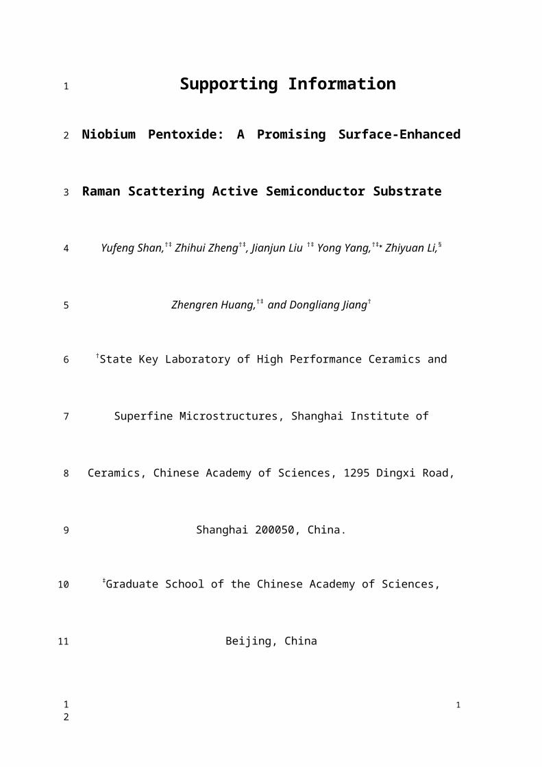
Figure S1. The SEM images of (a) Nb2O5, (b) TiO2 and (c) Ag substrates.
Figure S2. The UV-vis adsorption spectra of analytes solutions before and after
adsorption by Nb2O5 powders for (a) MeB, (b) MV and (c) MB.
2
1
2
3
4
5
12

Figure S3. The Raman spectra of MeB collected from six arbitrary Nb2O5
semiconductor substrates. For each substrate three different spots are randomly
selected.
Figure S4. (a) SERS signals of MV molecules with various concentrations excited by
3
1
2
3
4
5
6
12

the laser of 532 nm on Nb2O5 substrates. (b-c) Raman spectra of solid MV powders
and MV molecules with the concentration of 510-5 M collected on Nb2O5 substrates
under the excitation of 532 and 633 nm lasers, respectively.
Figure S5. (a) SERS signals of MB molecules with various concentrations excited by
the laser of 532 nm on Nb2O5 substrates. (b) Raman spectra of solid MB powders and
MB molecules with the concentration of 510-5 M collected on Nb2O5 substrates
under the excitation of 532 nm laser.
4
1
2
3
4
5
6
7
8
12

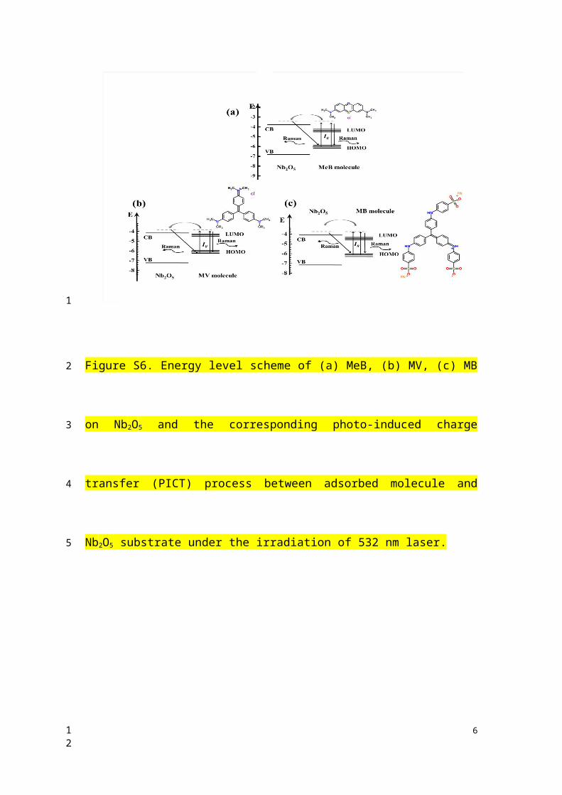
Figure S6. Energy level scheme of (a) MeB, (b) MV, (c) MB on Nb2O5 and the
corresponding photo-induced charge transfer (PICT) process between adsorbed
molecule and Nb2O5 substrate under the irradiation of 532 nm laser.
Figure S7 (a) The UV-vis optical absorption spectrum of pure Nb2O5 powders, MV
modified Nb2O5 powders and MV aqueous solution. (b) The UV-vis optical absorption
spectrum of pure Nb2O5 powders, MB modified Nb2O5 powders and MB aqueous
5
1
2
3
4
5
6
7
8
12
solution.
Scheme S1. Structure of analyte molecules of (a) MeB, (b) MV and (c) MB.
Scheme S2. (a) Three kinds of interaction sites with dye molecules on Nb2O5 surface.
(b) The negative net charges on the surface for Nb2O5 in alkalescent dye solutions.
6
1
2
3
4
5
6
7
8
12
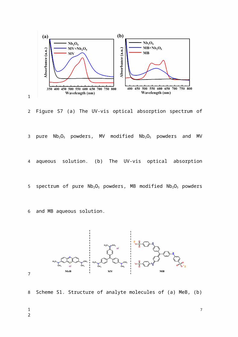
Table S1. Raman frequencies and corresponding assignments of the main bands
observed from the MeB solid powders and the SERS spectra by the excitation at 532
nm, 633 nm and 780 nm.[1]
Assignment Solid MeB
= 532 nm
Frequency,
cm-1
MeB-Nb2O5
= 532 nm
Frequency,
cm-1
Solid MeB
= 633 nm
Frequency,
cm-1
MeB-Nb2O5
= 633 nm
Frequency,
cm-1
Solid MeB
= 780 nm
Frequency,
cm-1
MeB-Nb2O5
= 780 nm
Frequency,
cm-1
(C-C)ring 1630 1632 1624 1622 1614 1621
(C-N)asym 1445 1441 1424
(C-N)sym 1370 1402 1398 1391 1394 1413
1307 1305 1298
(C-H) 1161 1155 1160 1151
1080 1077
(C-H) 1042 1042 1030 1035
955 957 946
866 864 890 894
832
813
775 774 773 770 767
(C-H) 674 667 667
(C-S-C) 618
(C-S-C) 597 601 598 592 598
564 554
(C-N-C) 506 504 505 496
466 472
(C-N-C) 453 453 449 442 447
(Nb-N) 252 250 247
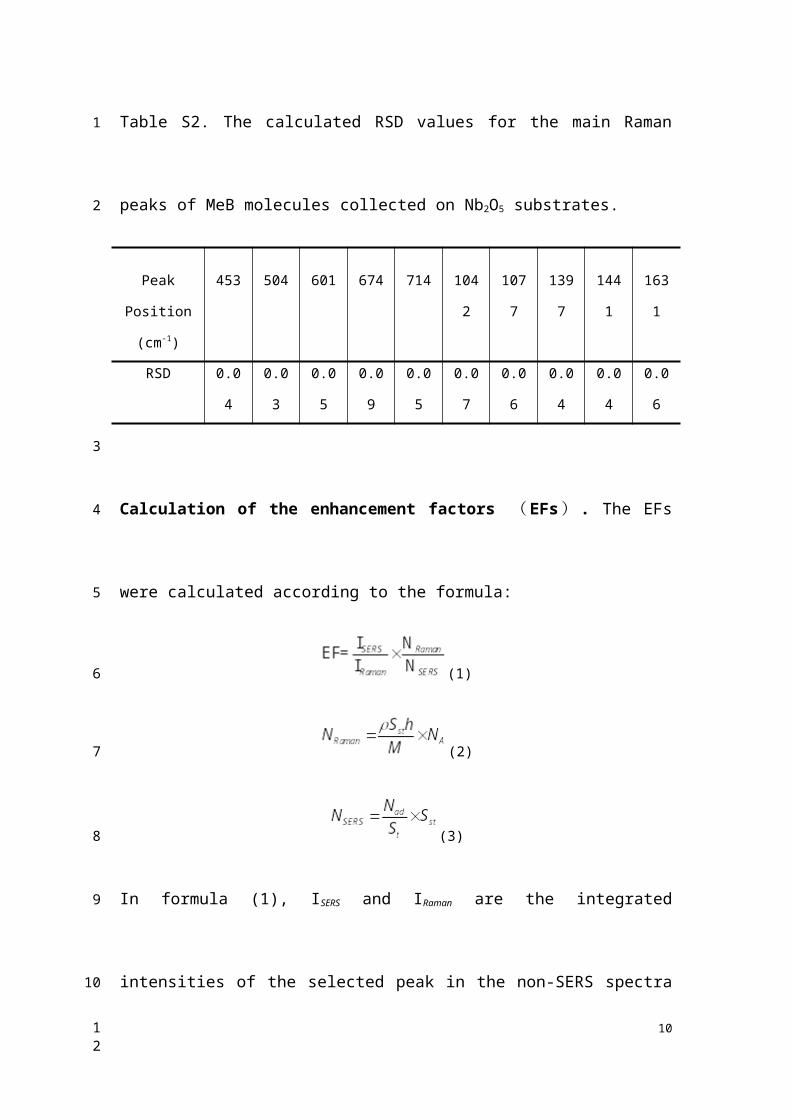
Table S2. The calculated RSD values for the main Raman peaks of MeB molecules
collected on Nb2O5 substrates.
Peak Position
(cm-1)
453 504 601 674 714 1042 1077 1397 1441 1631
RSD 0.04 0.03 0.05 0.09 0.05 0.07 0.06 0.04 0.04 0.06
7
1
2
3
4
5
6
7
12

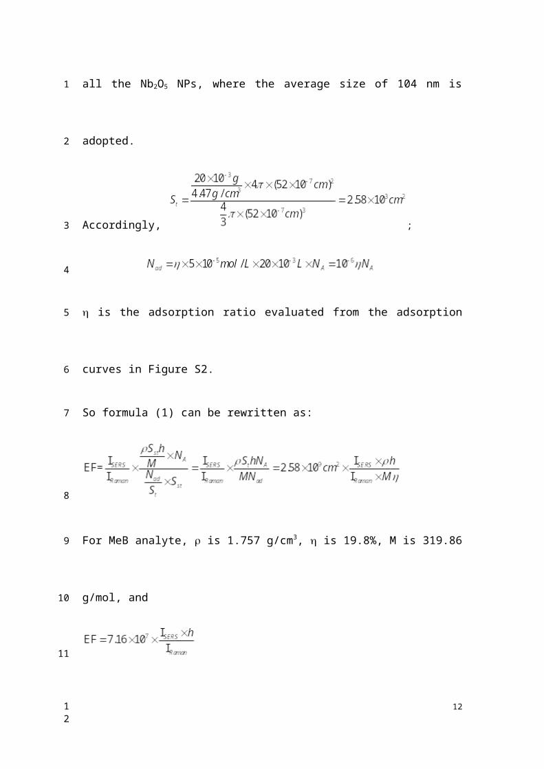
Calculation of the enhancement factors ( EFs) . The EFs were calculated
according to the formula:
(1)
(2)
(3)
In formula (1), ISERS and IRaman are the integrated intensities of the selected peak in the
non-SERS spectra of solid analyte powders and SERS spectra collected on the Nb2O5
substrates, and NSERS and NRaman are the corresponding average number of molecules in
scattering area for non-SERS and SERS spectra. In formula (2), , Sst, M and h refer
to the density of solid analytes, scattering area of irradiation laser, molecular weight
of analytes, and the confocal depth of the laser beam, respectively, while NA is the
Avogadro constant. In formula (3), Nad is the number of adsorbed analyte molecules to
Nb2O5 powder estimated from the adsorption curves in Figure S2, and S t is the total
surface area of all the Nb2O5 NPs, where the average size of 104 nm is adopted.
Accordingly, ;
is the adsorption ratio evaluated from the adsorption curves in Figure S2.
8
1
2
3
4
5
6
7
8
9
10
11
12
13
14
15
16
17
12

So formula (1) can be rewritten as:
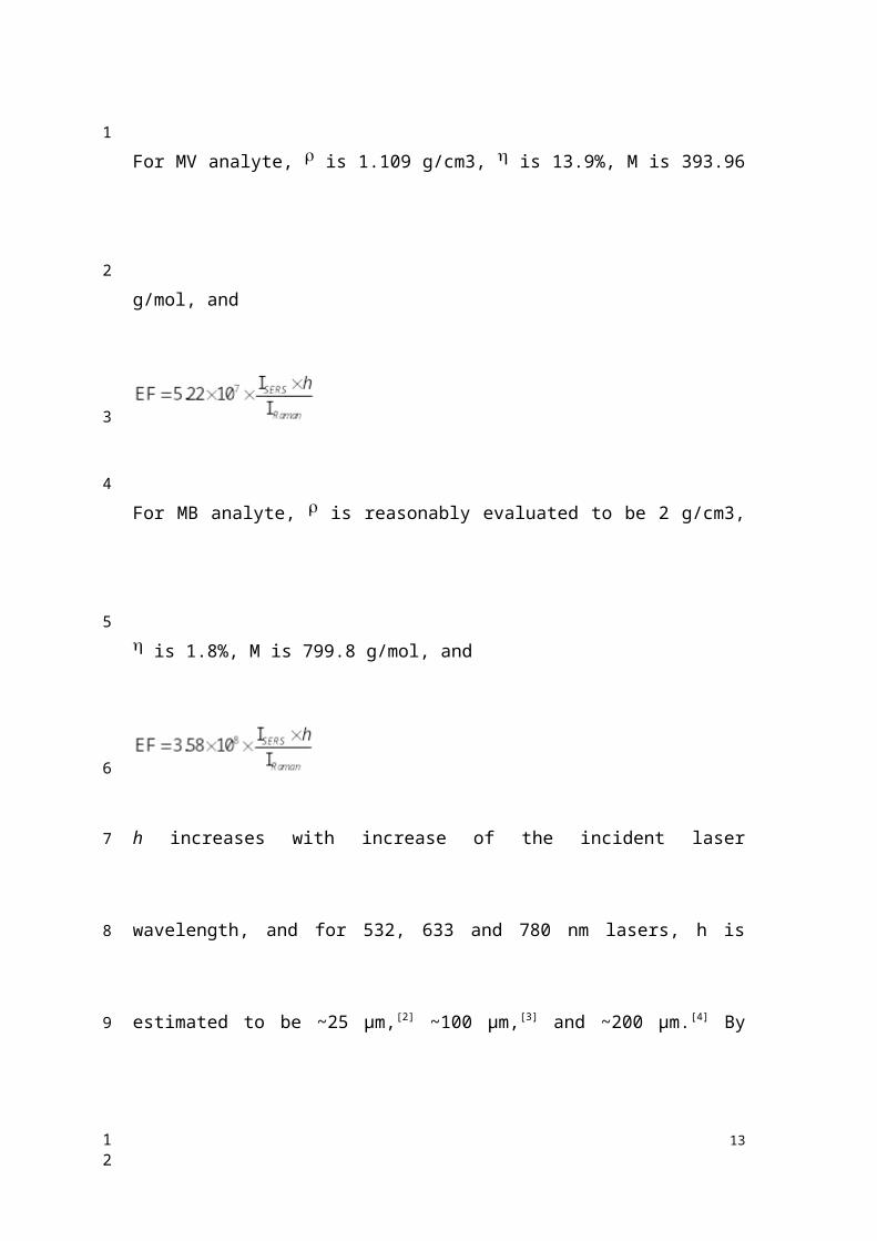
For MeB analyte, is 1.757 g/cm3, is 19.8%, M is 319.86 g/mol, and
For MV analyte, is 1.109 g/cm3, is 13.9%, M is 393.96 g/mol, and
For MB analyte, is reasonably evaluated to be 2 g/cm3, is 1.8%, M is 799.8
g/mol, and
h increases with increase of the incident laser wavelength, and for 532, 633 and 780
nm lasers, h is estimated to be ~25 μm,[2] ~100 μm,[3] and ~200 μm.[4] By utilizing
these parameters, the EFs with various excitation lasers for each analyte molecules
can be obtained.
The calculation of the contribution of photo-induced charge transfer (PICT) to
9
1
2
3
4
5
6
7
8
9
10
11
12
13
14
12
the molecular polarizability tensor in the semiconductor-molecule system
According to the Herzberg-Teller theory, the vibrational coupling of the conduction
band states |S and the valence band states |S' with the molecular ground states |I and
excited states |K is considered in the semiconductor-molecule system[5]. In our
system, the condition of ωSS'>ωIK is considered. The intensity of a Raman transition
(IRaman) could be expressed as the function of the molecular polarizability tensor:
Where I0 is the intensity of incident laser with an angular frequency of ω0, and ωIF is
the molecular transition frequency between states I and F (presumably two different
vibrational levels of the ground electronic state).
Considering the second-order perturbation, the polarizability tensor () could be
written as:
Where K represents all the other states of the molecule, μ is the dipole moment
operator, the μ and μ are the three-dimensional component in space (X, Y, Z). Taking
the zero-order Born-Oppenheimer approximation into account, all the states (I, K, F)
as the products of the electronic and vibrational wave functions can be written as:
10
1
2
3
4
5
6
7
8
9
10
11
12
13
14
15
16
17
18
12

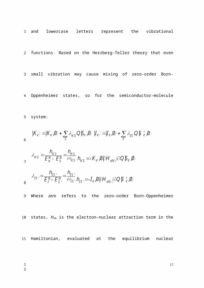
Where the subscript e indicates a pure electronic state, and lowercase letters represent
the vibrational functions. Based on the Herzberg-Teller theory that even small
vibration may cause mixing of zero-order Born-Oppenheimer states, so for the
semiconductor-molecule system:
Where zero refers to the zero-order Born-Oppenheimer states, HeN is the electron-
nuclear attraction term in the Hamiltonian, evaluated at the equilibrium nuclear
positions (0). |Se and |S'e indicates the electronic states lying in the conduction band
and valence band of semiconductor, respectively. hKS is the coupling matrix elements
representing the degree to which a particular vibration Q can mix state Se with the
state Ke. Similarly, hIS' is the coupling matrix element representing the degree to which
a particular vibration Q can mix states S'e with state Ie. For the purely electronic
transition moment between states, we write:
11
1
2
3
4
5
6
7
8
9
10
11
12
13
14
15
16
17
18
12
Next, we consider the situation that the energy gap between |S and |S' state for
semiconductor is larger than that between the |K and |I state for molecules. The
polarizability tensor in the semiconductor-molecule system can be rewritten as
follows (assuming that ω0>ωSS'):
= A+B+C
A represents the contribution of the molecular resonance to the polarizability tensor
via MIK.
B represents the contribution of photo-induced charge transfer of molecule-to-
semiconductor to the polarizability tensor via MIS. The transition borrows intensity
from the allowed transition MIK by means of vibrational coupling between the excited
12
1
2
3
4
5
6
7
8
9
10
11
12
13
12
molecular state K and semiconductor conduction band states S though the matrix
element hKS.
C represents the contribution of photo-induced charge transfer of semiconductor-to-
molecule to the polarizability tensor via MS'K. The transition borrows intensity from
the allowed transition MIK by means of vibrational coupling between the molecular
ground state I and semiconductor valence band states S' through the matrix element
hIS. This is illustrated in Scheme. S3(a).
Next, the situation that the frequency of exiting light is far from the semiconductor
electronic transition frequency (ωIK<ω0<ωSS') is considered. In term of A, the state K is
actually a semiconductor conduction band state S or the state I is actually a
semiconductor valance band state S'. Under this consideration the similar molecular
resonance contribution to the polarizability tensor can be expected. In this case, the
sum cannot be carried out over vibrational states k, and a single vibration will
dominate the sum. The polarizability tensor can be written as follows:
13
1
2
3
4
5
6
7
8
9
10
11
12
13
14
15
16
17
12
Ar is ascribed to the molecular resonance to the polarizability tensor via M IK. Am
represents similar molecular resonance contribution due to the photo-induced charge
transfer of molecule-to-semiconductor, which is from the molecular ground state I to
one of semiconductor conductor band states S. B' represents the contribution of the
photo-induced charge transfer of molecule-to-semiconductor, which is from the
molecular ground state I to one of the semiconductor conduction band states S. This
transition obtains its intensity via MIS through intensity borrowing from the (assumed)
allowed transition IK. The borrowing mechanism is vibrational coupling through hKS
which represents coupling of the semiconductor conduction band states S to the
molecular excited state K through some vibrational mode Q. This is illustrated in
Scheme S3(b). As represents similar molecular resonance contribution due to the
photo-induced charge transfer of semiconductor-to-molecule, which is from one of
semiconductor valence band states S' to the molecular excited state K. C' represents
the contributions of the photo-induced charge transfer of semiconductor-to-molecule,
which is from one of the semiconductor valence band states S' to the molecular
14
1
2
3
4
5
6
7
8
9
10
11
12
13
14
15
16
17
18
12

excited state K. This transition obtains its intensity via MS'K through intensity
borrowing from the (assumed) allowed transition IK. The borrowing mechanism is
vibrational coupling through hIS' which represents coupling of the semiconductor
valence band states S' to the molecular ground state I through some vibrational mode
Q. This is illustrated in Scheme S3(c).
Scheme S3. (a) The scheme for the photo-induced charge transfer of semiconductor-
to-molecule and molecule-to-semiconductor under the situation of ω0>ωss'. (b) The
scheme for the photo-induced charge transfer of semiconductor-to-molecule in
semiconductor-molecular system under the situation of ωIK<ω0<ωss'. (c) The scheme
15
1
2
3
4
5
6
7
8
9
10
11
12
12

for the photo-induced charge transfer of molecule-to-semiconductor in
semiconductor-molecular system under the situation of
ωIK<ω0<ωss'.
16
1
2
3
4
12
References
[1] G. Xiao, S. Man. Surface-enhanced Raman scattering of methylene blue adsorbed on cap-
shaped silver nanoparticles. Chem. Phys. Lett. 447(4–6): 305-309 (2007).
[2] W. Cai, B. Ren, X. Li, C. She, F. Liu, X. Cai, Z.-Q. Tian. Investigation of surface-enhanced
Raman scattering from platinum electrodes using a confocal Raman microscope: dependence
of surface roughening pretreatment. Surf.Sci. 406(1): 9-22 (1998).
[3] N. J. Everall. Confocal Raman microscopy: common errors and artefacts. Analyst 135(10):
2512-2522 (2010).
[4] A. Macdonald, A. Vaughan. Numerical simulations of confocal Raman spectroscopic depth
profiles of materials: a photon scattering approach. J. Raman Spectro. 38(5): 584-592 (2007).
[5] X. Wang, W. Shi, G. She, L. Mu. Using Si and Ge nanostructures as substrates for surface-
enhanced Raman scattering based on photoinduced charge transfer mechanism. J. Am. Chem.
Soc. 133(41): 16518-16523 (2011).
17
1
2
3
4
5
6
7
8
9
10
11
12
13
12