Embed Size (px)
Citation preview
Status of the FEE developments for
diamond detectors at GSI ‐ Detektorlabor
Mircea Ciobanu
GSI-Darmstadt, ISS-Bucharest
CARAT 2nd Workshop @ GSI13. - 15. December 2010

Outline
• A trial for the analytical model of the Diamond Detector – FEE Assemblies
• PADI‐4 , a fast Preamplifier‐Discriminator for Diamond Detectors
• DLNA, a Low Noise Amplifier for Diamonds Detectors
• Summary and Outlook

A trial for the analyticalmodel of the Diamond Detector – FEE Assemblies

The First Step: Detector ideal (the charge is instantaneously collected) and FEE consists just from
one resistor
VinpRiC D
iTR (t) inRi
colcolTR QtdtQtdti =⋅= ∫∫∞
∞−
∞
∞−
)()( δ
S-t/ τC eI(t)i 0= SCcol I(t)dtiQ τ⋅== ∫
∞
00
S-t/ τScolC e/τQ(t)i ⋅= DcolCiS CQ)(iRV /0 =⋅=
S-t/ τDcolS e/CQ(t)v ⋅=δ
inRin RifTkfTP ⋅=∆⋅⋅⋅=∆ 24),(Simplified equivalent schematic for noise estimations: DD is connected to a simple measurement device represented by the Ri resistor.
)/ff/(Rf/ifZf/i(f)V uSinRiNin nRi2222222 1∆)(∆ +⋅=⋅=
DDuSinRiNin CTkCT/kπ/fRf/iV /)4(42∆ 222 ⋅=⋅⋅⋅=⋅⋅⋅=SLUO LECTURE SERIES. LECTURE # 10H. SPIELER. December 18,1998
Acol
D
DAcol
Dt BWQ
CTkCBWQ
CTk⋅⋅⋅⋅
=⋅⋅
⋅=
28.2/28.2/
σ
Dcol CTkQNS ⋅⋅= //)//( dtdvnt σσ =trA =0.35/BWAdv/dt =0.8·Vs/trA=2.28· Qcol ·BWA/ CD

The Second Step: Detector ideal, FEE consists from one amp. with Noise Factor F and the frequency bandwidth BW
nRs
neq
nRs
neqnRs
ee
eeeF 2
2
2
22
1+=+
= nRsneq eFe 22 )1( ⋅−= nRsneq iFi 22 )1( ⋅−=
ineq RFTkfi /)1(4/2 −⋅⋅=∆ Dcol CFTkQNS ⋅−⋅⋅= )1(//
2/1220 )/1/()(
uAA ffGfG +=
]11[∆)()(∆ 222220
222222 )/ff()/ff(/GRf/ifGfZf/i(f)V uAuSinRiANou nRi +⋅+⋅⋅=⋅⋅=
)/1()1(2)/(∆
202
0222
SADuAuSuAuSinRiNou C
GFTkπ/ffffGRf/iVττ+⋅⋅−⋅⋅
=⋅+⋅⋅⋅⋅=

1)()( 00 ⋅=⋅=⋅= ∫∫∞
∞−
∞
∞−
GtdtGVtdtv AAA δτδA-t/
AA eV(t)v τδ ⋅=
∫∫∞
∞−
−∞
∞−
⋅⋅⋅=−=⊗= dueeVVduutvuvtvtv(t)v SAA u-t/ ASASASout
)/1/1()()()()( τττδδδδ
eG
CQtv
D
colMout
0)( ⋅=teGCQteVVtv AA -t/
AD
col-t/ ASout ⋅⋅⋅=⋅⋅⋅= ττ
τ0)(SA ττ =
)(1
1)( 1ln
1ln
0mm
mmm
D
colMout ee
mG
CQtv −−
⋅
−⋅−
⋅⋅=)()( 0AS -t/ t/
AS
S
D
colout eeG
CQtv ττ
τττ
−⋅−
⋅⋅= −
SA ττ ≠
)(11
)1(/ 1
ln1ln
mm
mmm
D
col eemm
CFTkQNS −−
⋅
−⋅−+
⋅⋅−⋅⋅
=)1(2
ln)1(2
ln1
11)1(
mmm
mm
col
DAt
ememm
QCFTk
−⋅⋅
−⋅ ⋅−
⋅+−
⋅⋅−⋅⋅⋅
=τ
σSA ττ =
SAm ττ /=

Results 1 for the Ideal case
S/N (left) and σt (right) as a function of CD with Ri as parameter

Results 2 for the Ideal case
S/N (left) and σt (right) as function of τA with CD as parameter

APLAC simulations for intuitive understanding of "ballistic deficit" errors
CD=1pF and τS =50ps, 500ps and 5ns CD=1pF and τS =500ps, 5ns and 50nsCD=0.1pF and τS =5ps, 50ps and 500ps
Simulated signals of a DD-FEE ensemble. Stars denote the detector output signals (referring to the left ordinate), triangles the corresponding BBA output signals (right ordinate). Three different values of Ri are shown (50Ω, 500Ω and 5KΩ) ; τA=50ps

The Third Step: The real detector is a scCVD diamond; we can apply the Shockley-Ramo theorem, for a parallel-plate detector
under the assumption of a homogenously distributed space charge :
heeff tt/ τhegenhe e
dEvQ
(t)i ./,,
)( τ−⋅=
where Qgen is the generated charge, v(E)e,h is the charge velocity, d is the detector thickness, τe,h denotes the lifetime of excess electrons and holes and τeff is given by
effheeff Nq ⋅⋅
⋅=
,
0
µεετ
with µe,h the effective mobility of electrons and holes, ε the diamond permittivity, ε0 the vacuum permittivity and q the elementary charge. Neff denotes the net effective fixed space charge in the diamond bulk. If the carrier lifetime is sufficiently long:
trdr t
dv = constt
Q(t)i
tr
genhe ==, for 0<t<ttr

coloutout Qtv(t)v /)(=δ duutiuvtitv(t)v heoutheoutP )()()()( ,, −⋅=⊗= ∫∞
∞−δ
a) for t<=ttr mmeme
tCGQ
(t)vAS -t/ t/
tr
S
D
genP −
−+⋅+−⋅⋅
⋅=
−
1)1(0
τττ
meemee
tCGQ
(t)vAtrAStrS / tt-t/ / ttt/
tr
S
D
genP −
−⋅+−−⋅⋅
⋅=
−−−−−
1))()(( )()(
0τττττ
b) for t>ttr
Transient response of a scCVD DD having ttr=5ns and three values of CD=0.1pF, 1pF and 10pF, for Ri=50Ω (left), Ri=500Ω (middle) and Ri=5KΩ (right).

)1(11
)1(/ meme
tmm
CFTkQ
NS AtrStr / -t/t
tr
S
D
gen −+⋅+−⋅⋅−+
⋅⋅−⋅⋅
= − τττ
)1(2ln
)1(2ln
11
1)1(
mm
mmm
gen
Dtrt
eem
mQ
CFTkt
−⋅−⋅⋅
−
⋅+−
⋅⋅−⋅⋅⋅
=σ
S/N ratio (left) and σt(right) as a function of CD, for three values of Ri.
S/N ratio (left) and σt(right) as a function of τA, for three values of CD .

Maximums:
τS1=1pF*5000Ω=5nsτS2=10pF*500Ω=5ns
in the analyzed case,ttr=5ns
The Signal/Noise ratio has a maximum for τS = collection time
Helmudt SpielerRadiation Detectors and Signal Processing (lecture series presented at University of Heidelberg, Oct. 10-14, 2005)http://www-physics.lbl.gov/~spieler/Heidelberg_Notes_Good lectures:2005/pdf/IV_Signal_Processing.pdf

PADIa fast PreAmplifier DIscriminator

Progress in
RPC
‐FEE
develop
men
t, CBM
Collabo
ratio
n Meetin
g Sept. 200
6
PADI : block diagram
DI
Tout+
Tout-
THR-
Threshold Voltage
THR+
Input+
Input-
Hys
Hyssteresis En/Dis
PA
Buffer
Eout+
Eout-
BiasIext
+1.8V
RextRext -
Rext
VSSVDD
0V
Bias Tout
+
Ch 1 - 4 Ch 1 - 4
Ch 1 - 4

Progress in
RPC
‐FEE
develop
men
t, CBM
Collabo
ratio
n Meetin
g Sept. 200
6
Preamplifier: AC equivalent diagram

Progress in
RPC
‐FEE
develop
men
t, CBM
Collabo
ratio
n Meetin
g Sept. 200
6
Discriminator: AC equivalent diagram
R3Cp3
TA5
R3Cp3
TA3
TA4
R2Cp2
TA2
R1
Cp1
Cp1Signal Input
R1
TA1
R2Cp2
Cp4R4
Rl
R4 Cp4
Cl
Output
Hyssteresis Enable/Disable

Linearity: Pulse MeasurementFirst results from
PADI, CB
M Collabo
ratio
n Meetin
g Febr. 2007
-10 -5 0 5 10-400
-300
-200
-100
0
100
200
300
PADI #2, Linearity, 5.5ns pulse applied at positive and negative inputs E
out_
diff
[mV
pk]
Uinp [mVpk]
Ch1 Ch2 Ch3
Linear Fit (-3mV - 3mV)for A BCh1 -2.79 57.7Ch2 -2.05 56.4Ch3 -2.29 54.7
Vthr_chip=100mV

Time over Threshold behavior First results from
PADI, CB
M Collabo
ratio
n Meetin
g Febr. 2007
1 10 100 10001
2
3
4
5
6
7
8
9
10 PADI #1, Short Pulse, Time over Threshold
ToT
[ns]
Uinp [mV]
Ch1 Ch2 Ch3

First results from
PADI‐2
, CBM
Collabo
ratio
n Meetin
g March. 2009
Time over Threshold behavior
1 10 100 1000
2.0
2.5
3.0
3.5
4.0
4.5
5.0
5.5
6.0
6.5
7.0
Ch1Ch2Ch3Ch4
Pul
sew
idth
[ns]
Uinp [mV]
VTHR
-chip [mV]
26 52 102 152 202 253

PADI-4A variant for Diamond detectors
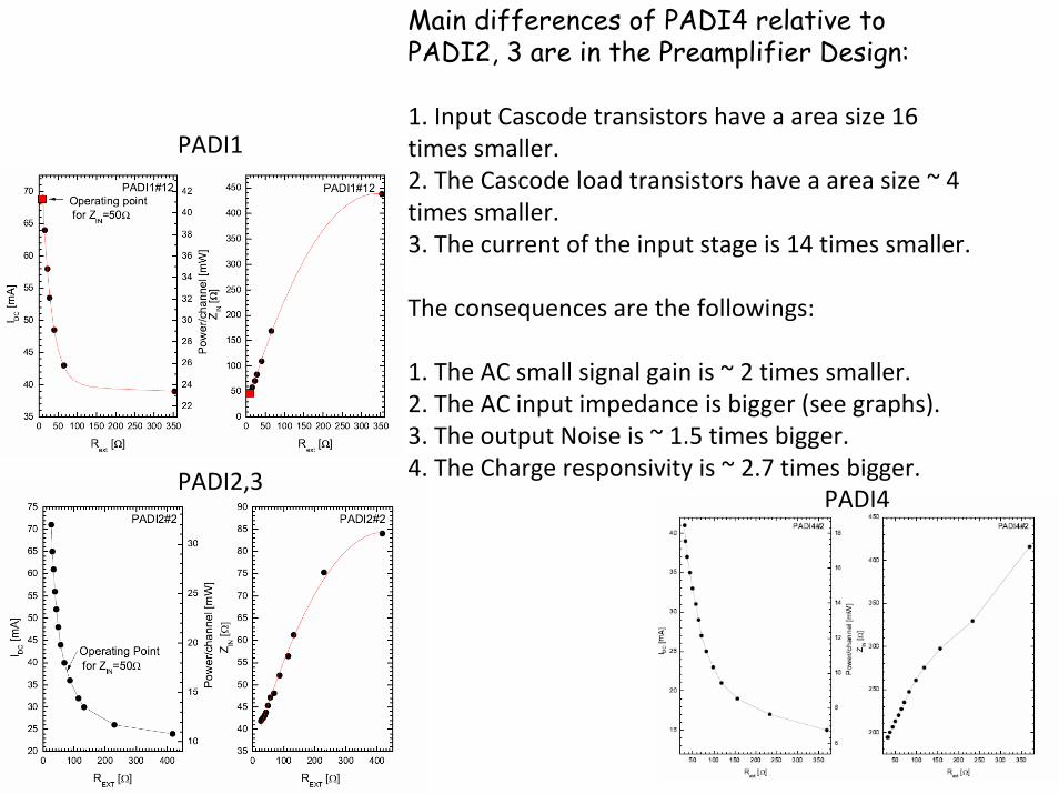
Main differences of PADI4 relative to PADI2, 3 are in the Preamplifier Design:
1. Input Cascode transistors have a area size 16 times smaller.2. The Cascode load transistors have a area size ~ 4 times smaller.3. The current of the input stage is 14 times smaller.
The consequences are the followings:
1. The AC small signal gain is ~ 2 times smaller.2. The AC input impedance is bigger (see graphs).3. The output Noise is ~ 1.5 times bigger.4. The Charge responsivity is ~ 2.7 times bigger.
PADI1
PADI2,3PADI4


PADI-5; Time Walk and Time over Thresholddependence to QIN and VTHR
PADI‐5 engineering review July 15, 2010, Detektorlabor, GSI‐Darmstadt

PADI-5 Transient response to QIN=2fC,at VTHR=2mV, for different temperatures (-20, 20, 60*C) and VDD (1.6, 1.8, 2.0 V)

DLNA(Diamond Low Noise Amplifier)

The BGU7003 MMIC is a wideband amplifier in SiGe:C technology from NXP Semiconductors (Philips)-2009: low noise and high gain, recommended for frequency interval 40MHz - 6GHz, made in large
scale, for handy's – low cost!.

DEVELOPMENT OF NEW PAD ASSEMBLIES (GSI)DEVELOPMENT OF NEW PAD ASSEMBLIES (GSI)DEVELOPMENT OF NEW PAD ASSEMBLIES (GSI)First laboratory tests with the new First laboratory tests with the new Diamond Low Noise Broadband Amplifier DLNBADiamond Low Noise Broadband Amplifier DLNBA
M. Ciobanu, M. Träger, S. Rahman, EBe
90Sr
Pulse Height [mV]0 2 4 6 8 10 12 14
CO
UN
TS
1
10
DoI CS886-1, 290µm@ -1.5 V/µm
DLNBA
90Sr avg pulse
t [ns]0 5 10 15
PU
LSE
HE
IGH
T [m
V]
-5
-4
-3
-2
-1
0
1DLNBA
DSO thr -3.5mV !!
HP3 Kick-Off, Paris Sep 2010 ADAMAS - Advanced Diamond Assemblies

DLNA through 0.4pF Step pulse excitation DBA2 through 1pF
DBAII- DBAII+ DLNA2- DLNA2+ RatioUOUT [mV] 63.3 -62.64 -57.03 57.76UIN [mV] -15.71 15.71 -15.71 15.71QIN [fC] 15.71 15.71 6.284 6.284RQVpk[mV/fC] -4.03 -3.99 9.08 9.19 2.3UN [mVrms] 1.600 1.600 1.306 1.306 0.82ENC [fC] 0.397 0.4 0.143 0.142 0.355tR [ns] 0.733 0.840 1.18 1.2 1.47tF [ns] 0.861 0.991 8.5 8.48 9.4AREA [pVs] 78.26 -92.52 -332 320.6 3.8RQVint [Ω] 5410 51870 9.6ZIN [Ω] ~50 ~470* meas. at 1/2 max 9.5
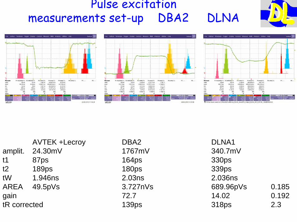
Pulse excitationmeasurements set-up DBA2 DLNA
AVTEK +Lecroy DBA2 DLNA1amplit. 24.30mV 1767mV 340.7mVt1 87ps 164ps 330pst2 189ps 180ps 339pstW 1.946ns 2.03ns 2.036nsAREA 49.5pVs 3.727nVs 689.96pVs 0.185gain 72.7 14.02 0.192tR corrected 139ps 318ps 2.3

Comparative Noise density measurements
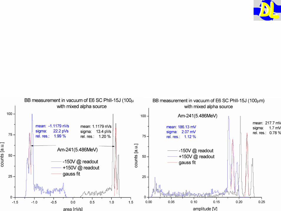

Tests with Alpha: DLNA with input protection (right) comparative to without (left)

• Summary• We have an analytical model of the
Diamond Detector – FEE Assemblies
PADI
• PADI-1 and -4 have been tested together with different diamond detectors and the differential connection is stable
• The use of Time over Threshold information for walk correction was tested in connection with the CAEN-TDC and real detector: works stable
• The connection PADI to the TDC-GET4 works (see Jochen Fruehauf talk).
DLNA
• The first tests are promising.• The Bandwidth specified in BGU7003 "Data
Sheets" is not reached yet.
• Outlook• We will try to complete the model with the
general case of the Shockley-Ramo theorem:
Then, the model will be very useful for DoIbetter understanding!
• When the Data Acquisition based on GET-4 will be finished, together with PADI will be a good candidate for multi channels diamond detection assemblies.
• We will continue to clarify the DLNA schematics to obtain the specified <6GHz Bandwidth. With the input protected and in the specified bandwidth, will be a good tool.
heeff tt/ τhegenhe e
dEvQ
(t)i ./,,
)( τ−⋅=
THANK YOU!