Embed Size (px)
Citation preview

Status of the Gallium Nitride High Electron Mobility Transistor
Radiation Testing for the NEPP ProgramLeif Scheick
Jet Propulsion Laboratory, California Institute of Technology, Pasadena, Ca
Copyright 2017 California Institute of Technology. U.S. Government sponsorship acknowledged. This research was carried out in part by the Jet Propulsion
Laboratory, California Institute of Technology, under contract with the National Aeronautics and Space Administration under the NASA Electronic Parts and
Packaging Program (Code AE). Other data was collected from NASA flight projects.

To be presented at the 8th NASA Electronic Parts and Packaging (NEPP) Program Electronic Technology Workshop June 26, 2017, NASA GSFC, Greenbelt, MD.
Current activities
• Working group discusses best methods for evaluating new wide band gap technologies for infusion into space– GRC, JPL, JSC, GSFC, AFRL– Monthly meeting to share data and resources for radiation
effects testing and reliability analyses• Previous efforts have been broad stroke testing
– Heavy ion testing• Gallium Nitride HEMTs (JPL)• Silicon Carbide MOSFETs (GSFC)
– Reliability screening• Temperature cycling of GaN and SiC
• On going and future efforts– Continues radiation testing and analysis– Reliability test screens for new devices– Guidelines for implementation and testing
To be presented at the 8th NASA Electronic Parts and Packaging (NEPP) Program Electronic Technology Workshop June 26, 2017, NASA GSFC, Greenbelt, MD.
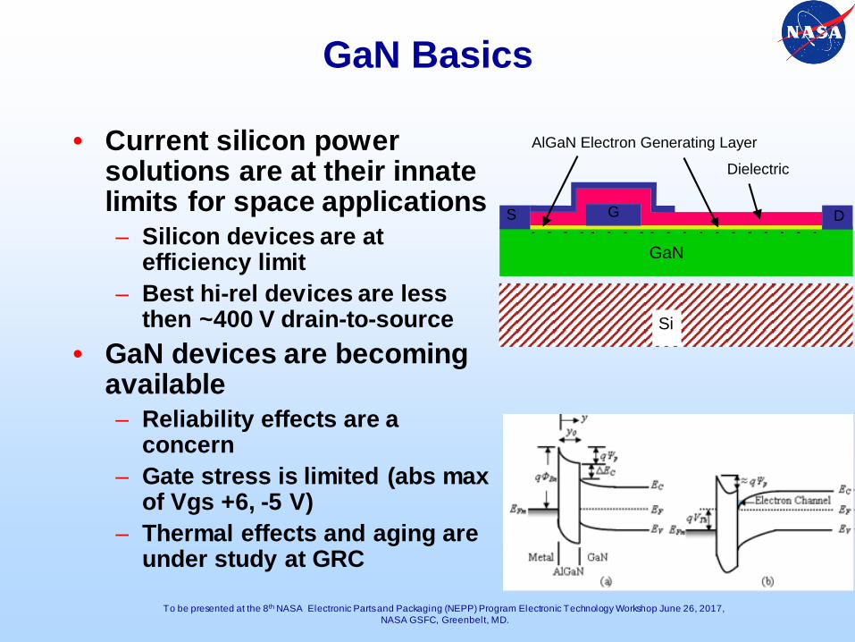
GaN Basics
• Current silicon power solutions are at their innate limits for space applications– Silicon devices are at
efficiency limit– Best hi-rel devices are less
then ~400 V drain-to-source• GaN devices are becoming
available– Reliability effects are a
concern– Gate stress is limited (abs max
of Vgs +6, -5 V)– Thermal effects and aging are
under study at GRC
Dielectric
GaN- - - - - - - - - - - - - - -
Si
AlGaN Electron Generating Layer
DGS- - - -
To be presented at the 8th NASA Electronic Parts and Packaging (NEPP) Program Electronic Technology Workshop June 26, 2017, NASA GSFC, Greenbelt, MD.
TESTING OF PANASONIC PARTS - CONTINUED
PGA26E19BA
To be presented at the 8th NASA Electronic Parts and Packaging (NEPP) Program Electronic Technology Workshop June 26, 2017, NASA GSFC, Greenbelt, MD.
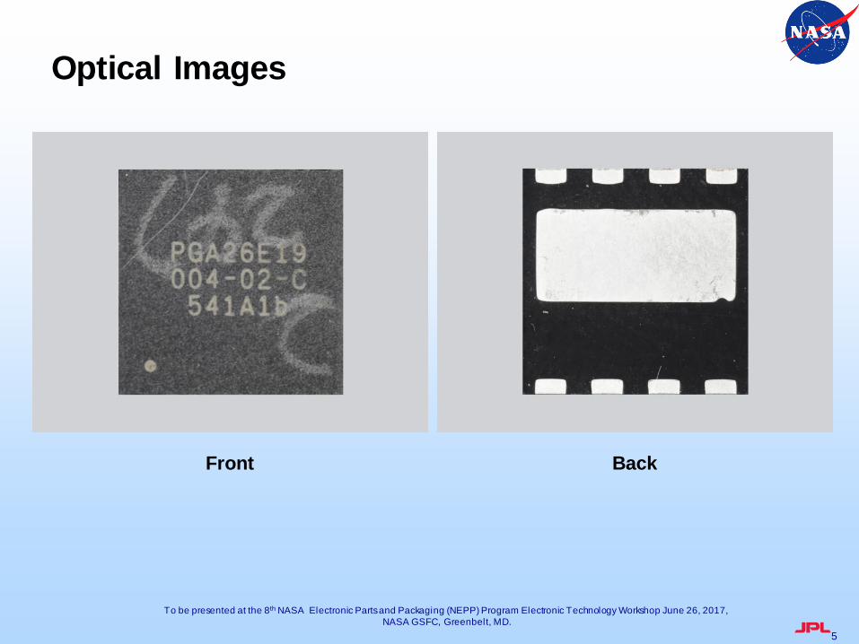
Optical Images
5
Front Back

To be presented at the 8th NASA Electronic Parts and Packaging (NEPP) Program Electronic Technology Workshop June 26, 2017, NASA GSFC, Greenbelt, MD.
Accomplishments
6
460µm
300µm
500µm
To be presented at the 8th NASA Electronic Parts and Packaging (NEPP) Program Electronic Technology Workshop June 26, 2017, NASA GSFC, Greenbelt, MD.
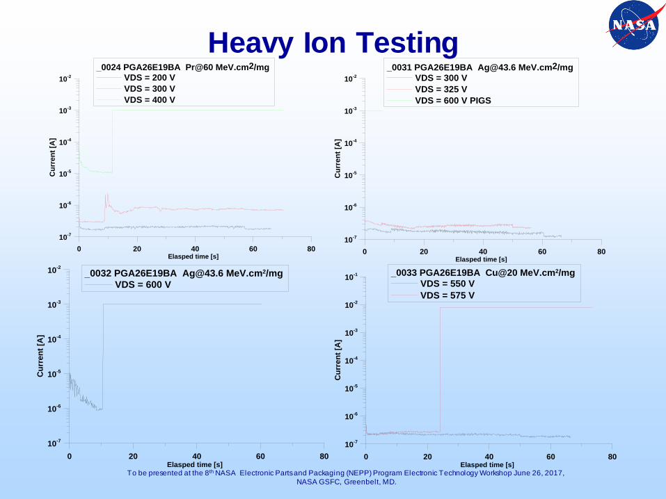
Heavy Ion Testing
0 20 40 60 80Elasped time [s]
10-7
10-6
10-5
10-4
10-3
10-2
Cur
rent
[A]
_0024 PGA26E19BA Pr@60 MeV.cm2/mg VDS = 200 VVDS = 300 VVDS = 400 V
0 20 40 60 80Elasped time [s]
10-7
10-6
10-5
10-4
10-3
10-2
Cur
rent
[A]
_0031 PGA26E19BA [email protected] MeV.cm2/mg VDS = 300 VVDS = 325 VVDS = 600 V PIGS
0 20 40 60 80Elasped time [s]
10-7
10-6
10-5
10-4
10-3
10-2
Cur
rent
[A]
_0032 PGA26E19BA [email protected] MeV.cm2/mg VDS = 600 V
0 20 40 60 80Elasped time [s]
10-7
10-6
10-5
10-4
10-3
10-2
10-1
Cur
rent
[A]
_0033 PGA26E19BA Cu@20 MeV.cm2/mg VDS = 550 VVDS = 575 V

To be presented at the 8th NASA Electronic Parts and Packaging (NEPP) Program Electronic Technology Workshop June 26, 2017, NASA GSFC, Greenbelt, MD.
Heavy Ion Testing
8
20 30 40 50 60
LET [MeV.cm2/mg]
200
300
400
500
600
Dra
in-to
-Sou
rce
(VD
S) [V
]
Average Pass Bias (VSEE) [V]for the PGA26E19BA
VGS=0 V
1 1.2 1.4 1.6 1.8 2
Inverse cosine of angle
0
100
200
300
400
Dra
in-to
-Sou
rce
(VD
S) [V
] Average Pass Bias (VSEE) [V] vs Inv Cosine of Angle
for the PGA26E19BAVGS=0 V
20 30 40 50 60
LET [MeV.cm2/mg]
10-7
10-6
Cro
ss S
ectio
n [c
m2 ] Cross section vs LET
for the PGA26E19BAVGS=0 V
1 1.2 1.4 1.6 1.8 2
Inverse cosine of angle
0
100
200
300
400
Dra
in-to
-Sou
rce
(Vds
) [V]
Average Pass Bias (Vds) [V] vs Inv Cosine of Anglefor the PGA26E19BA
VGS=0 V

To be presented at the 8th NASA Electronic Parts and Packaging (NEPP) Program Electronic Technology Workshop June 26, 2017, NASA GSFC, Greenbelt, MD.
Heavy Ion Testing
60 70 80 90 100
Change in range [um]
0
40
80
120
160
200
Cha
nge
in V
see
[V]
20
6044
Effect of ion range on Vseefor the PGA26E19BA
Point lables are LET in MeV-cm2/mg
10 20 30 40 50 60
LET [MeV.cm2/mg]
200
300
400
500
600
Dra
in-to
-Sou
rce
(Vds
) [V]
Average Pass Bias (Vds) [V]for the PGA26E19BA
VGS=0 V @ TAM VGS= 0 V @ BNL
Deeper ion penetration decreases Vsee

To be presented at the 8th NASA Electronic Parts and Packaging (NEPP) Program Electronic Technology Workshop June 26, 2017, NASA GSFC, Greenbelt, MD.
Heavy Ion Testing
-10 -8 -6 -4 -2 0
VGS [V]
320
360
400
440
480
Dra
in-to
-Sou
rce
(Vds
) [V]
Average Pass Bias (Vds) [V] vs Vgsfor the PGA26E19BA
LET = 44.6 MeV-cm2/mg and Normal Incidence
Gate-to-source voltage has no effect on Vsee
To be presented at the 8th NASA Electronic Parts and Packaging (NEPP) Program Electronic Technology Workshop June 26, 2017, NASA GSFC, Greenbelt, MD.
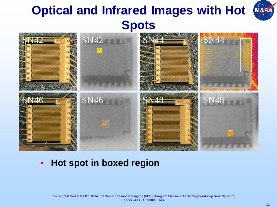
Optical and Infrared Images with Hot Spots
11
• Hot spot in boxed region
SN42 SN42 SN44 SN44
SN46 SN46 SN48 SN48

To be presented at the 8th NASA Electronic Parts and Packaging (NEPP) Program Electronic Technology Workshop June 26, 2017, NASA GSFC, Greenbelt, MD.
Optical and Infrared Images with Hot Spots
12
• Hot spot in boxed region
SN605 SN605 SN609 SN609
SN610 SN610a SN611 SN611

To be presented at the 8th NASA Electronic Parts and Packaging (NEPP) Program Electronic Technology Workshop June 26, 2017, NASA GSFC, Greenbelt, MD.
Failed Die Analysis
13
0.5mA @ 11V
1.2mA @ 8V
1uA @ 310V
400nA @ 615V
To be presented at the 8th NASA Electronic Parts and Packaging (NEPP) Program Electronic Technology Workshop June 26, 2017, NASA GSFC, Greenbelt, MD.
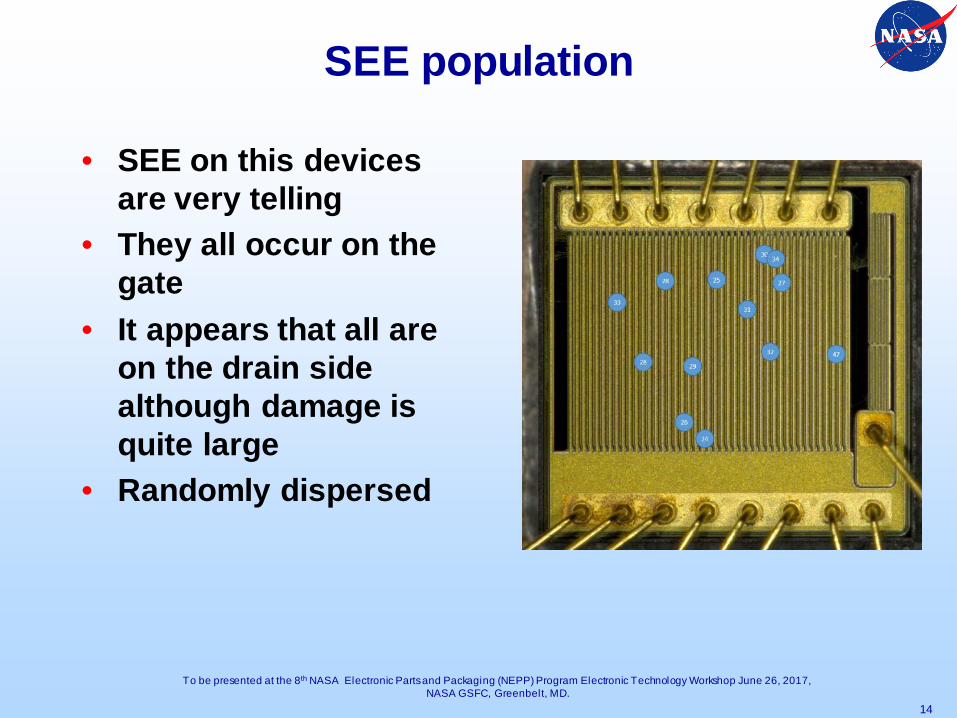
SEE population
• SEE on this devices are very telling
• They all occur on the gate
• It appears that all are on the drain side although damage is quite large
• Randomly dispersed
14
To be presented at the 8th NASA Electronic Parts and Packaging (NEPP) Program Electronic Technology Workshop June 26, 2017, NASA GSFC, Greenbelt, MD.
TESTING OF TRANSPHORMCASCODE HYBRIDS
TPH3208 and TPH3202
To be presented at the 8th NASA Electronic Parts and Packaging (NEPP) Program Electronic Technology Workshop June 26, 2017, NASA GSFC, Greenbelt, MD.
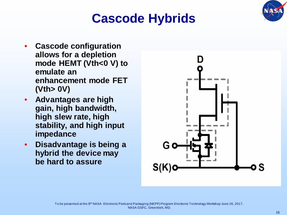
Cascode Hybrids
• Cascode configuration allows for a depletion mode HEMT (Vth<0 V) to emulate an enhancement mode FET (Vth> 0V)
• Advantages are high gain, high bandwidth, high slew rate, high stability, and high input impedance
• Disadvantage is being a hybrid the device may be hard to assure
16

To be presented at the 8th NASA Electronic Parts and Packaging (NEPP) Program Electronic Technology Workshop June 26, 2017, NASA GSFC, Greenbelt, MD.
Optical Images
17
TPS3202Gate Source Drain
TPH3208Gate Source Drain

To be presented at the 8th NASA Electronic Parts and Packaging (NEPP) Program Electronic Technology Workshop June 26, 2017, NASA GSFC, Greenbelt, MD.
Heavy Ion Testing
0 10 20 30 40Elasped time [s]
10-6
10-5
10-4
10-3
10-2
10-1
Cur
rent
[A]
_1334 TPH3208 [email protected] MeV.cm2/mg VDS = 50 V
These devices are very soft to ion damage
To be presented at the 8th NASA Electronic Parts and Packaging (NEPP) Program Electronic Technology Workshop June 26, 2017, NASA GSFC, Greenbelt, MD.
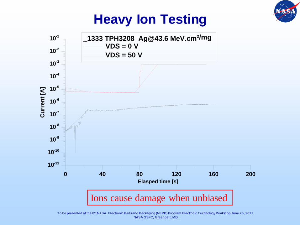
Heavy Ion Testing
0 40 80 120 160 200Elasped time [s]
10-11
10-10
10-9
10-8
10-7
10-6
10-5
10-4
10-3
10-2
10-1
Cur
rent
[A]
_1333 TPH3208 [email protected] MeV.cm2/mg VDS = 0 VVDS = 50 V
Ions cause damage when unbiased

To be presented at the 8th NASA Electronic Parts and Packaging (NEPP) Program Electronic Technology Workshop June 26, 2017, NASA GSFC, Greenbelt, MD.
Heavy Ion Testing
0 100 200 300 400 500Elasped time [s]
10-6
10-5
10-4
10-3
10-2
10-1
Cur
rent
[A]
_0638 TPH3202 Cu@20 MeV.cm2/mg VDS = 50 VVDS = 100 V
No incremental damage was seen
To be presented at the 8th NASA Electronic Parts and Packaging (NEPP) Program Electronic Technology Workshop June 26, 2017, NASA GSFC, Greenbelt, MD.
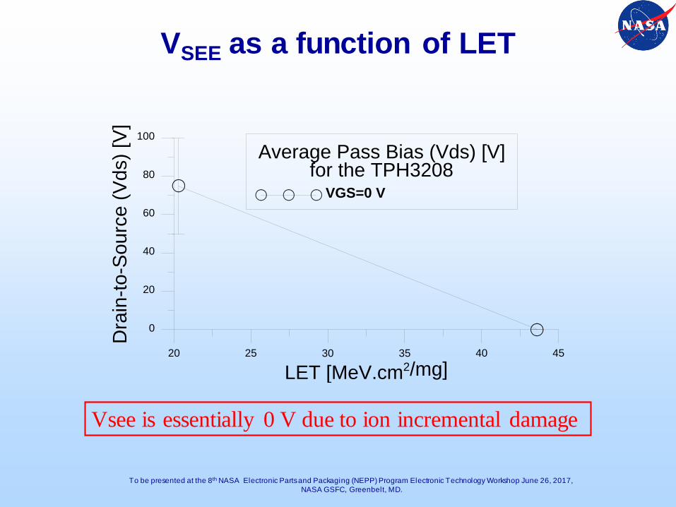
VSEE as a function of LET
20 25 30 35 40 45
LET [MeV.cm2/mg]
0
20
40
60
80
100D
rain
-to-S
ourc
e (V
ds) [
V]Average Pass Bias (Vds) [V]
for the TPH3208VGS=0 V
Vsee is essentially 0 V due to ion incremental damage

To be presented at the 8th NASA Electronic Parts and Packaging (NEPP) Program Electronic Technology Workshop June 26, 2017, NASA GSFC, Greenbelt, MD.
Cross-section as a function of LET
Cross-section is dependent on LET
20 25 30 35 40 45
LET [MeV.cm2/mg]
10-5
10-4
10-3
10-2
10-1C
ross
Sec
tion
[cm
2 ] Cross section vs LETfor the TPH3208
VGS=0 V

To be presented at the 8th NASA Electronic Parts and Packaging (NEPP) Program Electronic Technology Workshop June 26, 2017, NASA GSFC, Greenbelt, MD.
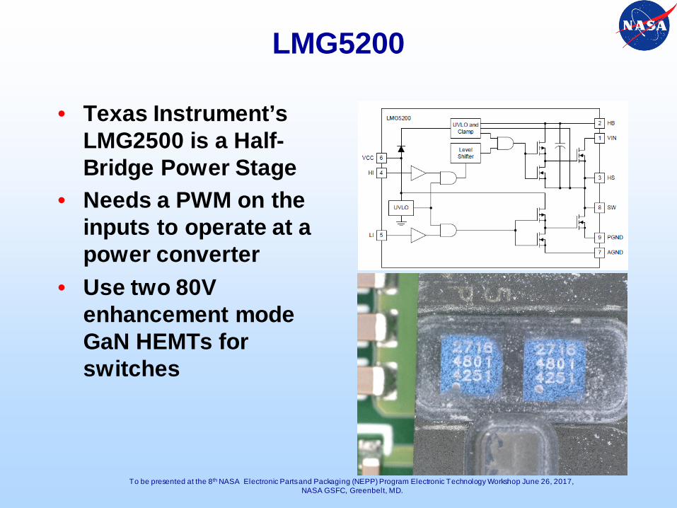
TESTING OF TI HYBRID POWER CONVERTER
LMG5200
To be presented at the 8th NASA Electronic Parts and Packaging (NEPP) Program Electronic Technology Workshop June 26, 2017, NASA GSFC, Greenbelt, MD.
LMG5200
• Texas Instrument’s LMG2500 is a Half-Bridge Power Stage
• Needs a PWM on the inputs to operate at a power converter
• Use two 80V enhancement mode GaN HEMTs for switches
To be presented at the 8th NASA Electronic Parts and Packaging (NEPP) Program Electronic Technology Workshop June 26, 2017, NASA GSFC, Greenbelt, MD.
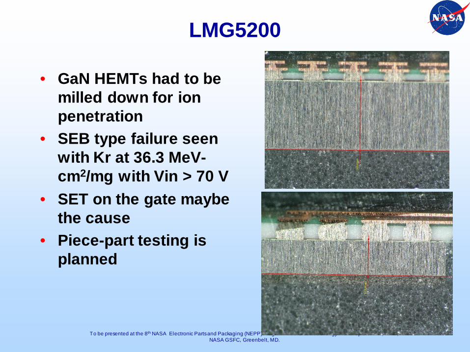
LMG5200
• GaN HEMTs had to be milled down for ion penetration
• SEB type failure seen with Kr at 36.3 MeV-cm2/mg with Vin > 70 V
• SET on the gate maybe the cause
• Piece-part testing is planned
To be presented at the 8th NASA Electronic Parts and Packaging (NEPP) Program Electronic Technology Workshop June 26, 2017, NASA GSFC, Greenbelt, MD.
FUTURE WORK

To be presented at the 8th NASA Electronic Parts and Packaging (NEPP) Program Electronic Technology Workshop June 26, 2017, NASA GSFC, Greenbelt, MD.
SEE Mechanism
• Since this effect is voltage dependent, we look to the spot with the largest electric field
• This is under the drain side of the gate
• A gate transient occur before an SEE
Dielectric
GaN- - - - - - - - - - - - - - -
Si
AlGaN Electron Generating Layer
DGS- - - -
Ion strike here?
Or here?
-10 0 10 20 30Elapsed Time [us]
-1
0
1
2
3
Cur
rent
[A]
SEE of EPC1012Vds=200 V, Vgs=0 V
Drain CurrentGate Current

To be presented at the 8th NASA Electronic Parts and Packaging (NEPP) Program Electronic Technology Workshop June 26, 2017, NASA GSFC, Greenbelt, MD.
SEE Mechanism
• The electric field magnitude extends into the GaN substrate
• Very narrow region of very high field
• Resulting strain on junction will make it easier to have SEE

To be presented at the 8th NASA Electronic Parts and Packaging (NEPP) Program Electronic Technology Workshop June 26, 2017, NASA GSFC, Greenbelt, MD.
More testing
• Panasonic parts– Best vehicle for mechanism investigation
• Transphorm– They are so soft, may also yield mechanism clue
• TI parts– TPS53632G and LMG3410 are on deck for SEE
• Freebird Semi– Resping of EPC product line – include higher voltage
parts – worth another look

To be presented at the 8th NASA Electronic Parts and Packaging (NEPP) Program Electronic Technology Workshop June 26, 2017, NASA GSFC, Greenbelt, MD.
Conclusion
• SEE in GaN HEMTs are complex– Mechanisms and underlying device physics are still
under study• New devices show similar effects
– Panasonic parts seem more robust– Transphorm devices show that GaN can be very soft
and there is no natural low voltage threshold• Future plans
– Body of Knowledge document with GRC– Testing guideline in works– Collaborate with NASA flight projects and external
customers