Embed Size (px)
Citation preview
[AP1037]
016016726-E-00 - 1 - 2017/01
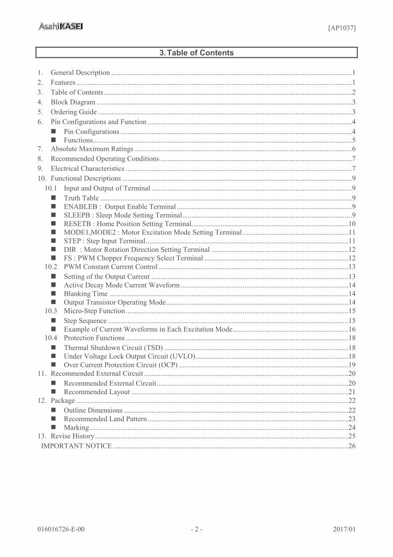
1. General DescriptionThe AP1037 is driver for bipolar stepper motors. It supports 35V motor power supply and 1.5A constant current operation. The AP1037 can automatically control Decay setting (slow, fast, pre-fast) in the IC inside by AKM original "Active Decay Control". The AP1037 can achieve optimal current setting, therefore will reduce current ripple and bring the motor rotation operation of the high efficiency. The input interface is clock-in method and supports from 2 Phase (full step) to 2W1-2 Phase (1/8step) excitation. In addition, the AP1037 is built-in a regulator for control circuit and capable of driving a motor only by motor power supplyvoltage (VM), therefore can facilitate design for the application.It is housed in a small QFN package with good heat dissipation performance, therefore the AP1037 is suitable for the stepping motor drive in a space-saving and high current.
2. Features
Built-in PWM current control stepper motor driver Active Decay ControlSingle Power Supply Operation Built-in Regulator for control circuitMotor Operating Voltage 8.0 to 35.0VMax Output Current 1.5AOn-Resistance (High+Low) 0.95 (typ.) @Ta=25Input Interface Clock-in methodExcitation Mode 2 Phase (Full step)
1-2 Phase (1/2 step) W1-2 Phase (1/4 step)2W1-2 Phase (1/8 step)
Selectable PWM chopper frequency 39kHz/77kHzSpike Noise Blanking Function Without an external noise filterPower Saving Function VM Power Consumption is less than10 A
(Ta=25°C)Selectable Motor Rotation Direction Forward/ReverseCorresponding to 3.3V/5V input signalBuilt-in Charge Pump CircuitUnder Voltage Lockout Circuit(UVLO)Thermal Shutdown Circuit (TSD)Over Current Protection Circuit (OCP)Operating Temperature Range -30 °C to +85°CPackage AP1037AER: 24-pin QFN (4.0mm )
AP1037AEN: 32-pin QFN (5.0mm )Pin Compatible Lineups AP1037AER, AP1037AEN : 1.5A
AP1034AER, AP1034AEN : 2.0AApplications MFP/LBP, Scanner, Robotics
ATM, Vending machines, Ticket machines, Moneychangers, Point of Sales System (POS) devices and etc.
Stepper Motor Driver IC equipped with Active Decay Control
AP1037
[AP1037]
016016726-E-00 - 2 - 2017/01
3.Table of Contents
1. General Description ....................................................................................................................................12. Features .......................................................................................................................................................13. Table of Contents ........................................................................................................................................24. Block Diagram ............................................................................................................................................35. Ordering Guide ...........................................................................................................................................36. Pin Configurations and Function ................................................................................................................4
Pin Configurations ...............................................................................................................................4Functions ..............................................................................................................................................5
7. Absolute Maximum Ratings .......................................................................................................................68. Recommended Operating Conditions .........................................................................................................79. Electrical Characteristics ............................................................................................................................710. Functional Descriptions ..............................................................................................................................9
10.1 Input and Output of Terminal ..............................................................................................................9Truth Table ..........................................................................................................................................9ENABLEB : Output Enable Terminal ................................................................................................9SLEEPB : Sleep Mode Setting Terminal .............................................................................................9RESETB : Home Position Setting Terminal ......................................................................................10MODE1,MODE2 : Motor Excitation Mode Setting Terminal ..........................................................11STEP : Step Input Terminal ...............................................................................................................11DIR : Motor Rotation Direction Setting Terminal ...........................................................................12FS : PWM Chopper Frequency Select Terminal ...............................................................................12
10.2 PWM Constant Current Control ........................................................................................................13Setting of the Output Current ............................................................................................................13Active Decay Mode Current Waveform ............................................................................................14Blanking Time ...................................................................................................................................14Output Transistor Operating Mode ....................................................................................................14
10.3 Micro-Step Function ..........................................................................................................................15Step Sequence ....................................................................................................................................15Example of Current Waveforms in Each Excitation Mode ...............................................................16
10.4 Protection Functions ..........................................................................................................................18Thermal Shutdown Circuit (TSD) .....................................................................................................18Under Voltage Lock Output Circuit (UVLO)....................................................................................18Over Current Protection Circuit (OCP) .............................................................................................19
11. Recommended External Circuit ................................................................................................................20Recommended External Circuit .........................................................................................................20Recommended Layout .......................................................................................................................21
12. Package .....................................................................................................................................................22Outline Dimensions ...........................................................................................................................22Recommended Land Pattern ..............................................................................................................23Marking ..............................................................................................................................................24
13. Revise History ...........................................................................................................................................25IMPORTANT NOTICE .................................................................................................................................26
[AP1037]
016016726-E-00 - 3 - 2017/01
4.Block Diagram
MODE1
RESET_B
CH
OSC
TSD
Charge Pump
H-Bridge 2Exposed Pad
SLEEP_B
MODE2
GND
DIR
STEP
OUT1B
OUT1A
RIS1
OUT2B
OUT2A
RIS2
VM1VM
High-Side Gate Drive
VM
CVG
CHL
CL
H-Bridge 1
IS1
IS2
VG
PreDriver
UVLO(VM)
NC
Regulator
VDC
CVDC
ControlLogic
Low-Side Gate Drive
Imt.VDC
Blank Time&
PWM Control
Active Decay Control
Transltor
VREF
RR2
RR1
MCU
DAC
IS1
IS2
FS
OCP
1 8
CMP1
CMP2
VM2VM
VM
Figure 1. Block Diagram
5.Ordering Guide
AP1037AER -30°C to +85°C 24-pin QFNAP1037AEN -30°C to +85°C 32-pin QFN
ENABLEB
SLEEPB
RESETB
[AP1037]
016016726-E-00 - 4 - 2017/01
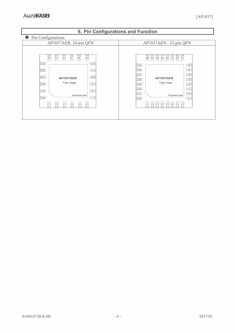
6. Pin Configurations and FunctionPin Configurations
AP1037AER: 24-pin QFN AP1037AEN : 32-pin QFN
[AP1037]
016016726-E-00 - 5 - 2017/01
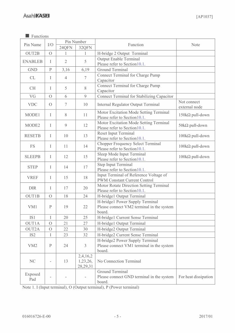
Functions
Pin Name I/OPin Number
Function Note24QFN 32QFN
OUT2B O 1 1 H-bridge 2 Output Terminal
ENABLEB I 2 5 Output Enable TerminalPlease refer to Section10.1.
GND P 3,16 6,19 Ground Terminal
CL I 4 7 Connect Terminal for Charge PumpCapacitor
CH I 5 8 Connect Terminal for Charge PumpCapacitor
VG O 6 9 Connect Terminal for Stabilizing Capacitor
VDC O 7 10 Internal Regulator Output Terminal Not connect external node
MODE1 I 8 11 Motor Excitation Mode Setting TerminalPlease refer to Section10.1. 150 pull-down
MODE2 I 9 12 Motor Excitation Mode Setting TerminalPlease refer to Section10.1. 5 -down
RESETB I 10 13 Reset Input TerminalPlease refer to Section10.1. 100 pull-down
FS I 11 14 Chopper Frequency Select TerminalPlease refer to Section10.1. 100 -down
SLEEPB I 12 15 Sleep Mode Input TerminalPlease refer to Section10.1. 100 -down
STEP I 14 17 Step Input TerminalPlease refer to Section10.1.
VREF I 15 18 Input Terminal of Reference Voltage of PWM Constant Current Control
DIR I 17 20 Motor Rotate Direction Setting TerminalPlease refer to Section10.1.
OUT1B O 18 24 H-bridge1 Output Terminal
VM1 P 19 22H-bridge1 Power Supply TerminalPlease connect VM2 terminal in the systemboard.
IS1 I 20 25 H-bridge1 Current Sense TerminalOUT1A O 21 27 H-bridge1 Output TerminalOUT2A O 22 30 H-bridge2 Output Terminal
IS2 I 23 32 H-bridge2 Current Sense Terminal
VM2 P 24 3H-bridge2 Power Supply TerminalPlease connect VM1 terminal in the systemboard.
NC - 132,4,16,21,23,26,28,29,31
No Connection Terminal
Exposed Pad - - -
Ground TerminalPlease connect GND terminal in the systemboard.
For heat dissipation
Note 1. I (Input terminal), O (Output terminal), P (Power terminal)

[AP1037]
016016726-E-00 - 6 - 2017/01
7.Absolute Maximum Ratings
Parameter Symbol min max Unit ConditionMotor Power Supply Voltage VM -0.5 35 V Digital Input/Output Terminal Voltage(STEP, DIR, RESETB, MODE1,MODE2, ENABLEB, SLEEPB, FS)
Vterm1 -0.5 5.5 V
VM Level Terminal Voltage(OUT1A,OUT1B, OUT2A,OUT2B) Vterm2 -0.5 VM V
VG,CH Terminal Voltage Vterm3 VM-0.5
VM+5.5 V The Min value must not
exceed -0.5V.VDC Terminal Voltage VDC -0.4 5.5 V VREF Input Voltage VREF -0.5 VDC VCL Terminal Voltage VCL -0.5 VDC VIS1,IS2 Terminal Voltage ISn -0.5 1.5 VOutput Current Iload - 2.0 A (Note 3,Note 4)
Power Dissipation32QFN PD1
- 3.9 W Ta=25°C (Note 4, Note 5)- 2.0 W Ta=85°C (Note 4, Note 5)
24QFN PD2- 3.1 W Ta=25°C (Note 4, Note 5)- 1.6 W Ta=85°C (Note 4, Note 5)
Junction Temperature Tj - 150 °CStorage Temperature Tstg -40 150 °CNote 2. All above voltages are with respect to GND. The each power supply of VC and VM is sequence-free.Note 3. For Power Dissipation, the output current rating may be limited by duty cycle, Ta, and PCB board heat
sinking design.Note 4. Exposed Pad must be connected to GND. Note 5. A 4-layer JEDEC51 compliant board is used.
If the temperature exceeds 25°C, be sure to derate at Figure 2.24-pin QFN: JA =40°C /W32-pin QFN: JA =32°C /W
WARNING: Operation at or beyond these limits may result in permanent damage to the device. Normal operation is not guaranteed at these extremes.
Figure 2. Maximum Power Dissipation

[AP1037]
016016726-E-00 - 7 - 2017/01
8.Recommended Operating Conditions
Parameter Symbol min typ max Unit NoteMotor Power Supply Voltage VM 8.0 24.0 35.0 VMaximum Output Current(Continuous) Iload - - 1.5 A (Note 6)
Reference Voltage of PWM Constant Current Control VREF 0.0 - 3.6 V Iload(100%)[A]=(VREF/8)/RISn
Operating Temperature Range Ta -30 - 85 °CNote 6. Please have a thermal design so as not exceed Tj = 150 degrees and Power Dissipation.Note 7. All voltages are with respect defined to GND (Exposed-Pad).
9.Electrical Characteristics (Ta = 25°C, VM=24V, unless otherwise specified.)
Parameter Symbol Condition min typ max UnitQuiescent Current
VM Quiescent Current
IVMENABLEB=”L” SLEEPB=”H” - - 12.0 mA
IVMOFFENABLEB=”H” SLEEPB=”H” - - 7.0 mA
IVMPSVSLEEPB=”L” SLEEP MODE - 10 30 A
H-bridge Circuit
Driver On Resistance RON Iload = 1.12A - 0.95 1.28
Body Diode Forward Voltage VF IF = 0.1A - 0.8 1.2 V
Interface
Input High Level Voltage VIH 2.0 - - V
Input Low Level Voltage VIL - - 0.8 V
Input Hysteresis
(Note 9) Vhys STEP, DIR, RESETB,
MODE1,MODE2,ENABLEB 0.2 0.4 V
Input Pulse Rise Time tR - - 1.0 s
Input Pulse Fall Time tF - - 1.0 s
Input High Level Current IIHSTEP,DIR, ENABLEB 5.5V applying -1.0 - 1.0 A
Input Low Level Current IIL 0V applying -1.0 - 1.0 A
Reference Voltage
VREF Input Voltage Range VREF 0 - 3.6 V
VREF Input Current IVREF VREF=2V -3 - 3 A
[AP1037]
016016726-E-00 - 8 - 2017/01
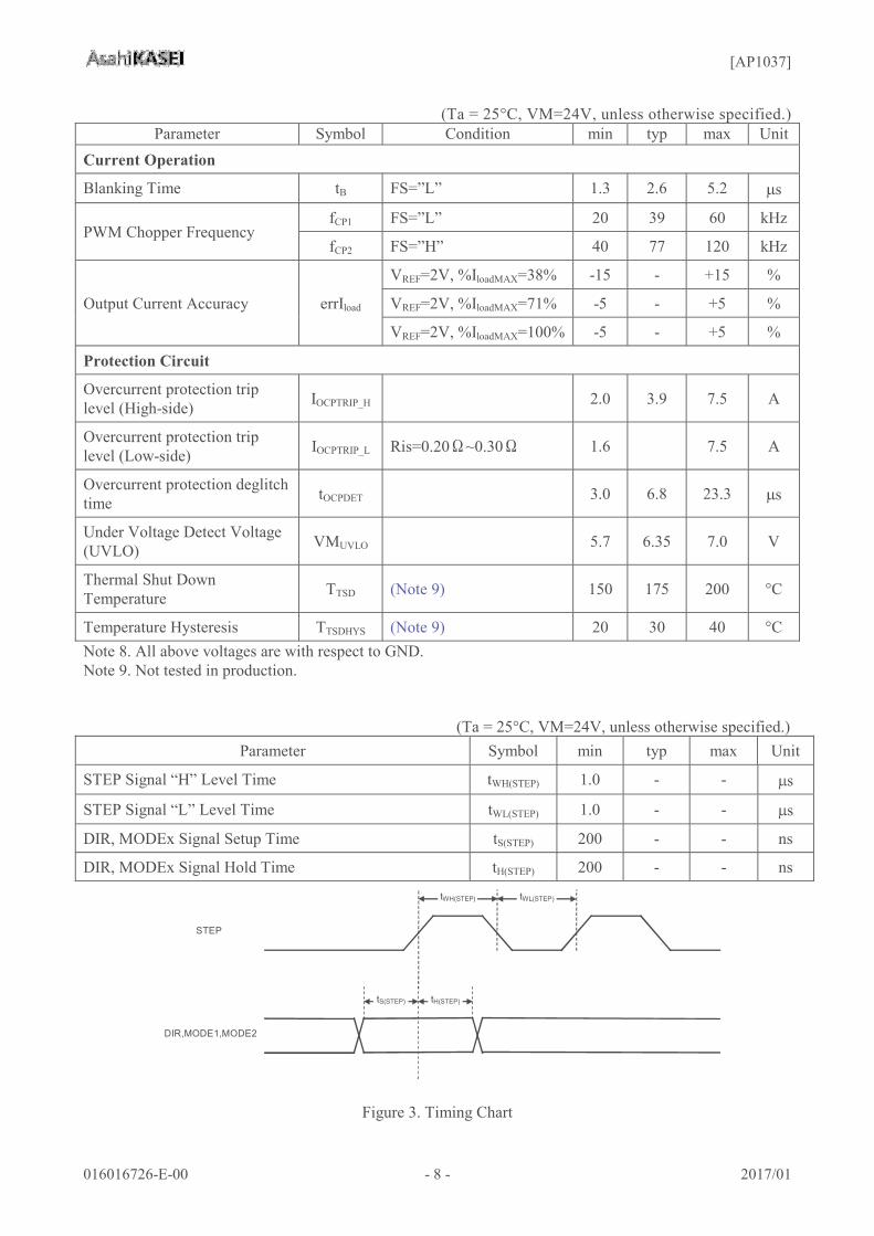
(Ta = 25°C, VM=24V, unless otherwise specified.) Parameter Symbol Condition min typ max Unit
Current Operation
Blanking Time tB FS=”L” 1.3 2.6 5.2 s
PWM Chopper Frequency fCP1 FS=”L” 20 39 60 kHz
fCP2 FS=”H” 40 77 120 kHz
Output Current Accuracy errIload
VREF=2V, %IloadMAX=38% -15 - +15 %
VREF=2V, %IloadMAX=71% -5 - +5 %
VREF=2V, %IloadMAX=100% -5 - +5 %
Protection Circuit
Overcurrent protection trip level (High-side) IOCPTRIP_H 2.0 3.9 7.5 A
Overcurrent protection trip level (Low-side) IOCPTRIP_L Ris=0.20 ~0.30 1.6 7.5 A
Overcurrent protection deglitch time tOCPDET 3.0 6.8 23.3 s
Under Voltage Detect Voltage(UVLO) VMUVLO 5.7 6.35 7.0 V
Thermal Shut Down Temperature TTSD (Note 9) 150 175 200 °C
Temperature Hysteresis TTSDHYS (Note 9) 20 30 40 °CNote 8. All above voltages are with respect to GND. Note 9. Not tested in production.
(Ta = 25°C, VM=24V, unless otherwise specified.) Parameter Symbol min typ max Unit
STEP Signal “H” Level Time tWH(STEP) 1.0 - - s
STEP Signal “L” Level Time tWL(STEP) 1.0 - - s
DIR, MODEx Signal Setup Time tS(STEP) 200 - - ns
DIR, MODEx Signal Hold Time tH(STEP) 200 - - ns
tWH(STEP) tWL(STEP)
STEP
tS(STEP) tH(STEP)
DIR,MODE1,MODE2
Figure 3. Timing Chart
[AP1037]
016016726-E-00 - 9 - 2017/01
10. Functional Descriptions
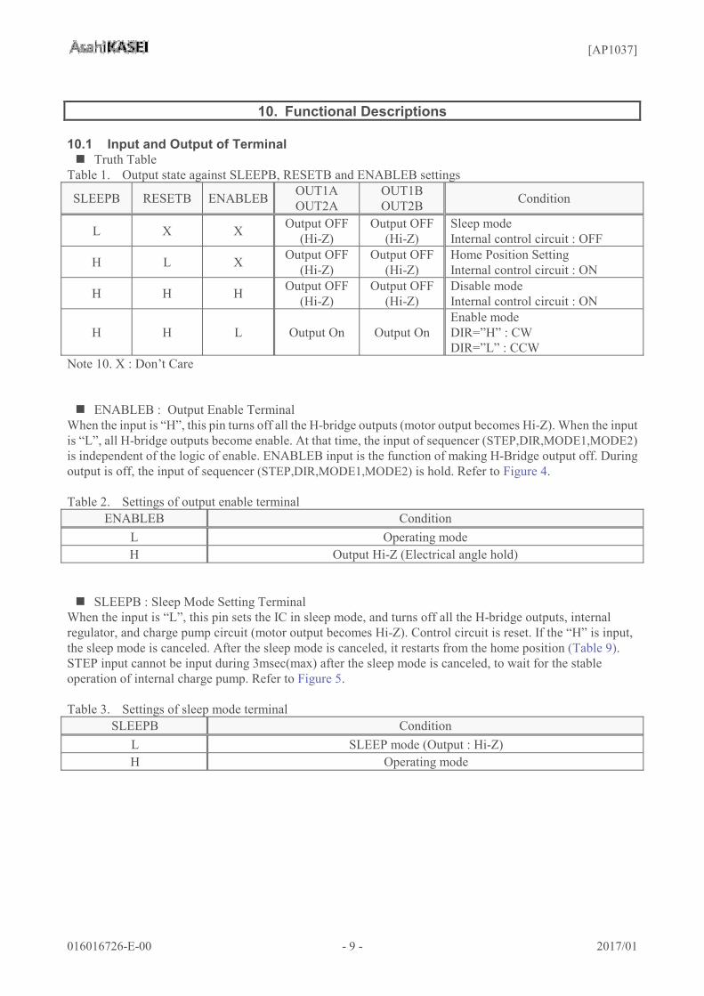
10.1 Input and Output of Terminal Truth Table
Table 1. Output state against SLEEPB, RESETB and ENABLEB settings
SLEEPB RESETB ENABLEB OUT1AOUT2A
OUT1BOUT2B Condition
L X X Output OFF(Hi-Z)
Output OFF(Hi-Z)
Sleep modeInternal control circuit : OFF
H L X Output OFF(Hi-Z)
Output OFF(Hi-Z)
Home Position SettingInternal control circuit : ON
H H H Output OFF(Hi-Z)
Output OFF(Hi-Z)
Disable modeInternal control circuit : ON
H H L Output On Output On Enable modeDIR=”H” : CWDIR=”L” : CCW
Note 10. X : Don’t Care
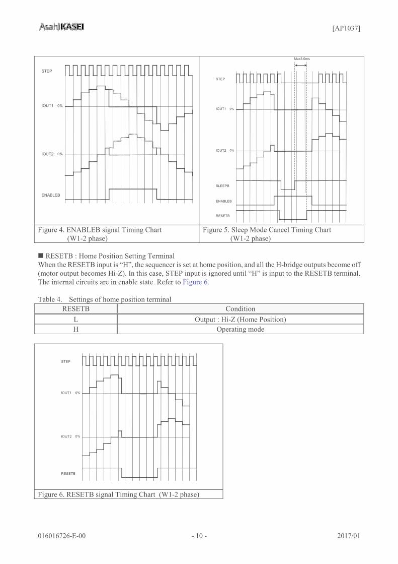
ENABLEB : Output Enable TerminalWhen the input is “H”, this pin turns off all the H-bridge outputs (motor output becomes Hi-Z). When the input is “L”, all H-bridge outputs become enable. At that time, the input of sequencer (STEP,DIR,MODE1,MODE2)is independent of the logic of enable. ENABLEB input is the function of making H-Bridge output off. During output is off, the input of sequencer (STEP,DIR,MODE1,MODE2) is hold. Refer to Figure 4.
Table 2. Settings of output enable terminal ENABLEB Condition
L Operating modeH Output Hi-Z (Electrical angle hold)
SLEEPB : Sleep Mode Setting TerminalWhen the input is “L”, this pin sets the IC in sleep mode, and turns off all the H-bridge outputs, internal regulator, and charge pump circuit (motor output becomes Hi-Z). Control circuit is reset. If the “H” is input, the sleep mode is canceled. After the sleep mode is canceled, it restarts from the home position (Table 9).STEP input cannot be input during 3msec(max) after the sleep mode is canceled, to wait for the stable operation of internal charge pump. Refer to Figure 5.
Table 3. Settings of sleep mode terminalSLEEPB Condition
L SLEEP mode (Output : Hi-Z)H Operating mode
[AP1037]
016016726-E-00 - 10 - 2017/01
STEP
IOUT1
ENABLEB
IOUT2
0%
0%
STEP
IOUT1
SLEEPB
IOUT2
0%
0%
Max3.0ms
ENABLEB
RESETB
Figure 4. ENABLEB signal Timing Chart(W1-2 phase)
Figure 5. Sleep Mode Cancel Timing Chart(W1-2 phase)
RESETB : Home Position Setting TerminalWhen the RESETB input is “H”, the sequencer is set at home position, and all the H-bridge outputs become off(motor output becomes Hi-Z). In this case, STEP input is ignored until “H” is input to the RESETB terminal.The internal circuits are in enable state. Refer to Figure 6.
Table 4. Settings of home position terminal RESETB Condition
L Output : Hi-Z (Home Position)H Operating mode
STEP
IOUT1
RESETB
IOUT2
0%
0%
Figure 6. RESETB signal Timing Chart (W1-2 phase)
[AP1037]
016016726-E-00 - 11 - 2017/01
MODE1,MODE2 : Motor Excitation Mode Setting TerminalThe MODE1 and MODE2 terminals are used to configure stepping format as shown below.
Table 5. Settings of MODE terminals that excite motorMODE1 MODE2 Excitation mode
L L 2 phase (Full step)H L 1-2 phase (1/2step)L H W1-2 phase (1/4step)H H 2W1-2phase (1/8step)
STEP : Step Input TerminalThe sequencer operates at the rising edge of the STEP input, electrical angle will proceed one at each step. Please design the pattern such that there is no jump of noise in STEP input terminal.
Table 6. Step excitation state against STEP input STEP Condition
Rising Edge Sends excitation stepFalling Edge Hold excitation step
[AP1037]
016016726-E-00 - 12 - 2017/01
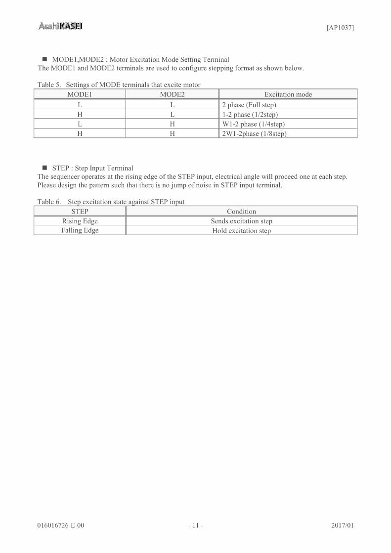
DIR : Motor Rotation Direction Setting TerminalThis pin sets the direction of motor rotation. When changing the direction, a new setting is reflected on a rising edge of the CLK pin. Refer to Figure 7.
CCW : H-bridge2 current is output by shifting 90deree ahead against the H-bridge1 current. CW : H-bridge2 current is output by shifting 90degree behind against the H-bridge1 current.
Table 7. Settings of rotate direction of motor DIR Condition
L CCW (Reverse)H CW (Forward)
STEP
IOUT1
DIR
IOUT2
0%
0%
CCWCW CW
Figure 7. DIR signal Timing Chart (W1-2 phase)
FS : PWM Chopper Frequency Select TerminalBy inputting “H” to the FS input, it is possible to drive the PWM chopper frequency in 77kHz (typ). By inputting “L” or connecting GND, PWM chopper frequency becomes 39kHz (typ).Please decide the setting of the FS input “50us” before than the ENABLEB input is set to "L".
Table 8. Settings of PWM chopper frequency select terminalFS ConditionL fCP=39kHz(typ)H fCP=77kHz(typ)

[AP1037]
016016726-E-00 - 13 - 2017/01
10.2 PWM Constant Current ControlSetting of the Output Current
The frequency of the internal OSC circuit is used to drive a stepper motor in PWM constant current controlling. The maximum current value (Setting Current = Trip Current) is determined by a sense resistance (RIS) for sensing current and the input voltage to the VREF pin (VREF).
Iload (100%) [A]= (VREF /8) / RIS VREF : PWM constant current setting voltage RIS : H-Bridge sense resistor VREF damping ratio : 1/8
Calculation example1 VREF=2.4V, RIS=0.24ohm Iload (100%)[A] = (2.4 / 8) / 0.24ohm = 1.25A
Please use the resistance that is smaller than a resistance value to show in below for current sense resistance.
Figure 8. Recommended Sense Resistor
[AP1037]
016016726-E-00 - 14 - 2017/01
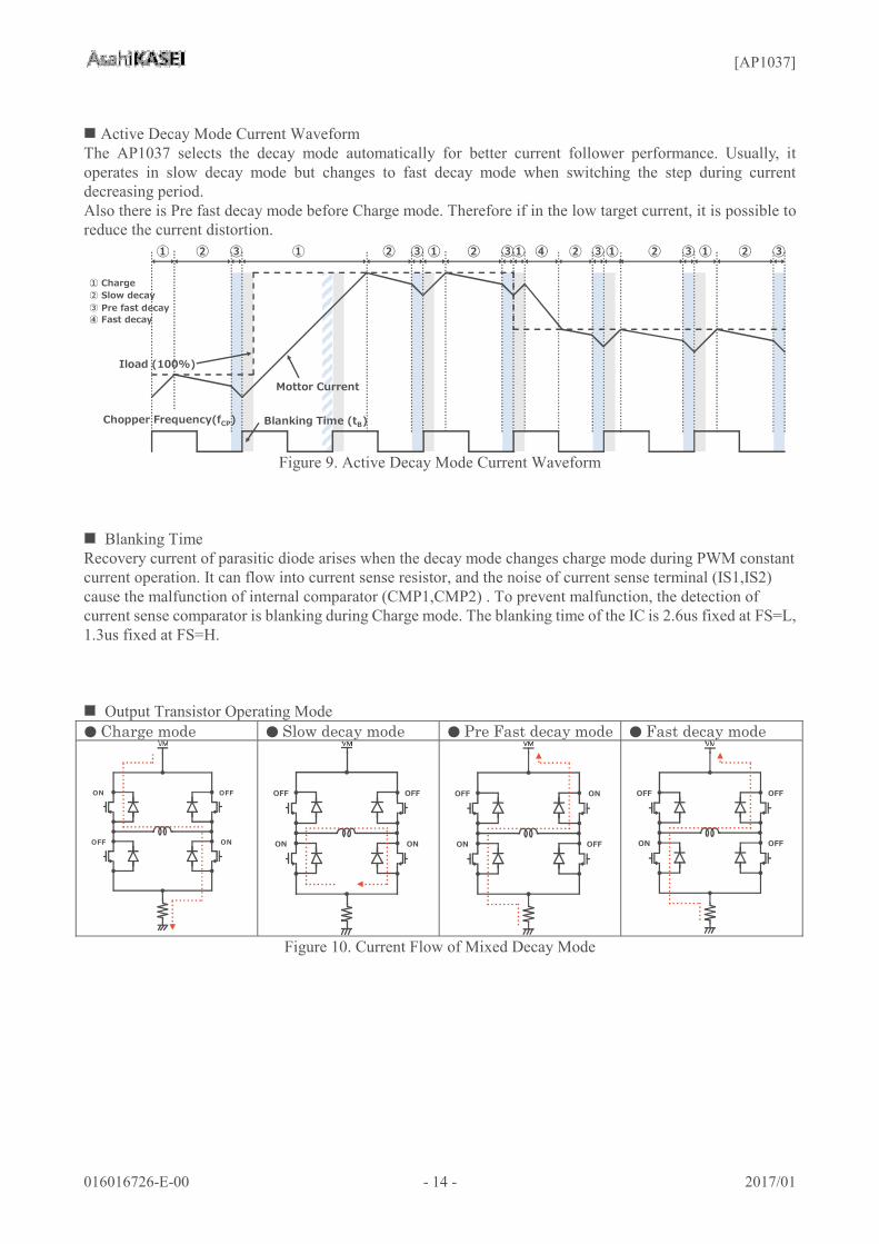
Active Decay Mode Current WaveformThe AP1037 selects the decay mode automatically for better current follower performance. Usually, itoperates in slow decay mode but changes to fast decay mode when switching the step during current decreasing period.Also there is Pre fast decay mode before Charge mode. Therefore if in the low target current, it is possible to reduce the current distortion.
Iload (100%)
Chopper Frequency(fCP)
Mottor Current
ChargeSlow decayPre fast decayFast decay
Blanking Time (tB)
Figure 9. Active Decay Mode Current Waveform
Blanking Time Recovery current of parasitic diode arises when the decay mode changes charge mode during PWM constant current operation. It can flow into current sense resistor, and the noise of current sense terminal (IS1,IS2) cause the malfunction of internal comparator (CMP1,CMP2) . To prevent malfunction, the detection of current sense comparator is blanking during Charge mode. The blanking time of the IC is 2.6us fixed at FS=L, 1.3us fixed at FS=H.
Output Transistor Operating Mode Charge mode Slow decay mode Pre Fast decay mode Fast decay mode
ON OFF
OFF ON
OFF OFF
ON ON
OFF ON
ON OFF
OFF OFF
ON OFF
Figure 10. Current Flow of Mixed Decay Mode

[AP1037]
016016726-E-00 - 15 - 2017/01
10.3 Micro-Step FunctionStep Sequence
Table 9. Setting Current Comparison of Excitation Modes
2 phase (Full step)
1-2 phase (1/2step)
W1-2 phase (1/4step)
2W1-2 phase (1/8step)
Phase1Current
[%Iloadmax]
Phase2Current
[%Iloadmax]
Step Angle [°]
1 1 1 100 0 0.002 98 20 11.25
2 3 92 38 22.504 83 56 33.75
1 2 3 5 71 71 45.006 56 83 56.25
4 7 38 92 67.508 20 98 78.75
3 5 9 0 100 90.0010 -20 98 101.25
6 11 -38 92 112.5012 -56 83 123.75
2 4 7 13 -71 71 135.0014 -83 56 146.25
8 15 -92 38 157.5016 -98 20 168.75
5 9 17 -100 0 180.0018 -98 -20 191.25
10 19 -92 -38 202.5020 -83 -56 213.75
3 6 11 21 -71 -71 225.0022 -56 -83 236.25
12 23 -38 -92 247.5024 -20 -98 258.75
7 13 25 0 -100 270.0026 20 -98 281.25
14 27 38 -92 292.5028 56 -83 303.75
4 8 15 29 71 -71 315.0030 83 -56 326.25
16 31 92 -38 337.5032 98 -20 348.75
: Home micro-step position at Step Angle 45°Note 11. When the excitation mode is changed to a coarser mode, it is set to the closest position in the rotate direction set by DIR signal. However, the motor could step-out or misstep depends on the operation state of motor during switching time. The changing sequence of the excitation mode should be determined by adequate evaluation.
Table 10. When changing to 2phase excitation mode at eighth position from 2W1-2phase excitation mode
DIRBefore After2W1-2 2phase(4step)
H 8step position 2step positionL 8step position 1step position
[AP1037]
016016726-E-00 - 16 - 2017/01
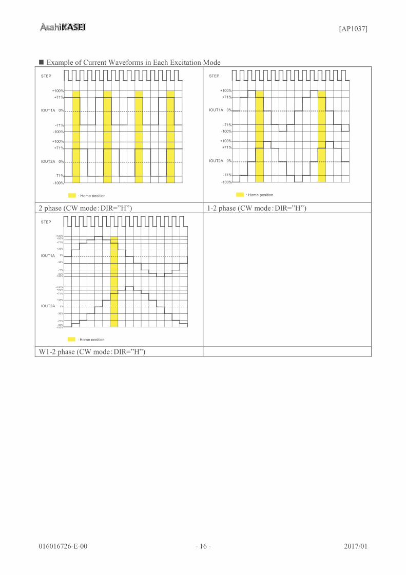
Example of Current Waveforms in Each Excitation Mode
STEP
IOUT2A 0%
+100%
IOUT1A 0%
+100%
-100%
-100%
+71%
-71%
+71%
-71%
: Home position
STEP
IOUT2A 0%
+100%
IOUT1A 0%
+100%
-100%
-100%
+71%
-71%
+71%
-71%
: Home position
2 phase (CW mode DIR=”H”) 1-2 phase (CW mode DIR=”H”)
STEP
IOUT2A
IOUT1A
: Home position
0%
+100%
-100%
+71%
-71%
+38%
-38%
+92%
-92%
0%
+100%
-100%
+71%
-71%
+38%
-38%
+92%
-92%
W1-2 phase (CW mode DIR=”H”)
[AP1037]
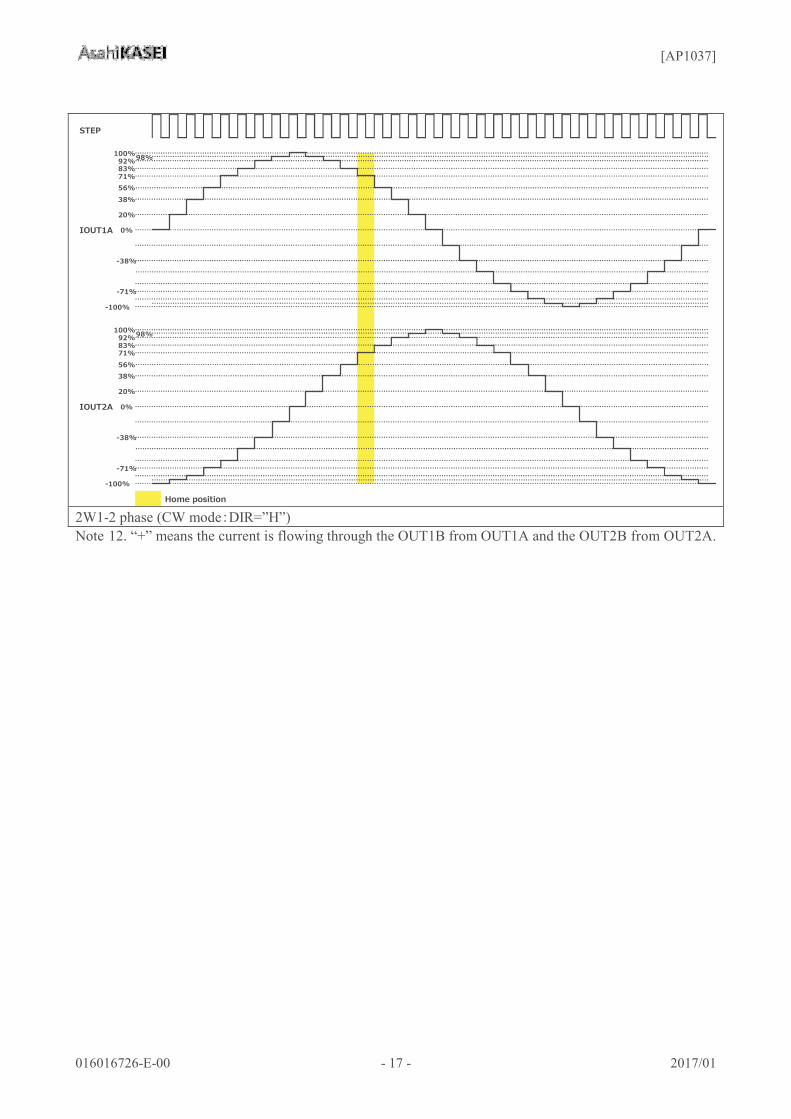
016016726-E-00 - 17 - 2017/01
100%98%92%83%71%56%38%
20%
0%
‒100%
‒38%
‒71%
100%98%92%83%71%56%38%
20%
0%
‒100%
‒38%
‒71%
STEP
IOUT1A
IOUT2A
Home position
2W1-2 phase (CW mode DIR=”H”)Note 12. “+” means the current is flowing through the OUT1B from OUT1A and the OUT2B from OUT2A.

[AP1037]
016016726-E-00 - 18 - 2017/01
10.4 Protection Functions Table 11. Recovery type and the output state of the protection circuit
Protection Circuit H-Bridge Outputs Recovery typeThermal Shutdown (TSD) Hi-Z AutomaticUnder Voltage Lockout (UVLO) Hi-Z Automatic
Over Current Protection (OCP)
Shorted-LoadHi-Z Latch off Shorted-to-Ground
Shorted-to-Power
Thermal Shutdown Circuit (TSD)
If the internal temperature of the IC (Tj) reaches 175 °C (typ), the H-Bridge outputs Hi-Z. In addition, it will automatically return to the normal operation when it becomes less than 145 °C (typ).
VOUT ON
TJ TTSD
OFF(HI-Z)
TTSD+TTSDHYS
ON
TTSDHYS
Figure 11. TSD Timing Chart
Under Voltage Lock Output Circuit (UVLO)
When VM voltage is lower than 6.35V (typ), the H-Bridge output is the Hi-Z. Please note that this circuit does not operate during sleep mode. When UVLO operates, internal circuits which includes H-Bridge output, internal regulator, charge pump circuit become disable, and also the control circuit is reset (initialize). If VM voltage goes up than the specified voltage, UVLO is released. After the UVLO released, it restarts from the home position. STEP input cannot be input during 3msec after the UVLO is canceled, to wait for the stable operation of internal charge pump.
VOUT
ON OFF(Hi‒Z) ON
VMHYS=0.5V(typ)VMUVLO
VM
3ms(max)
Figure 12. UVLO Timing Chart
[AP1037]
016016726-E-00 - 19 - 2017/01
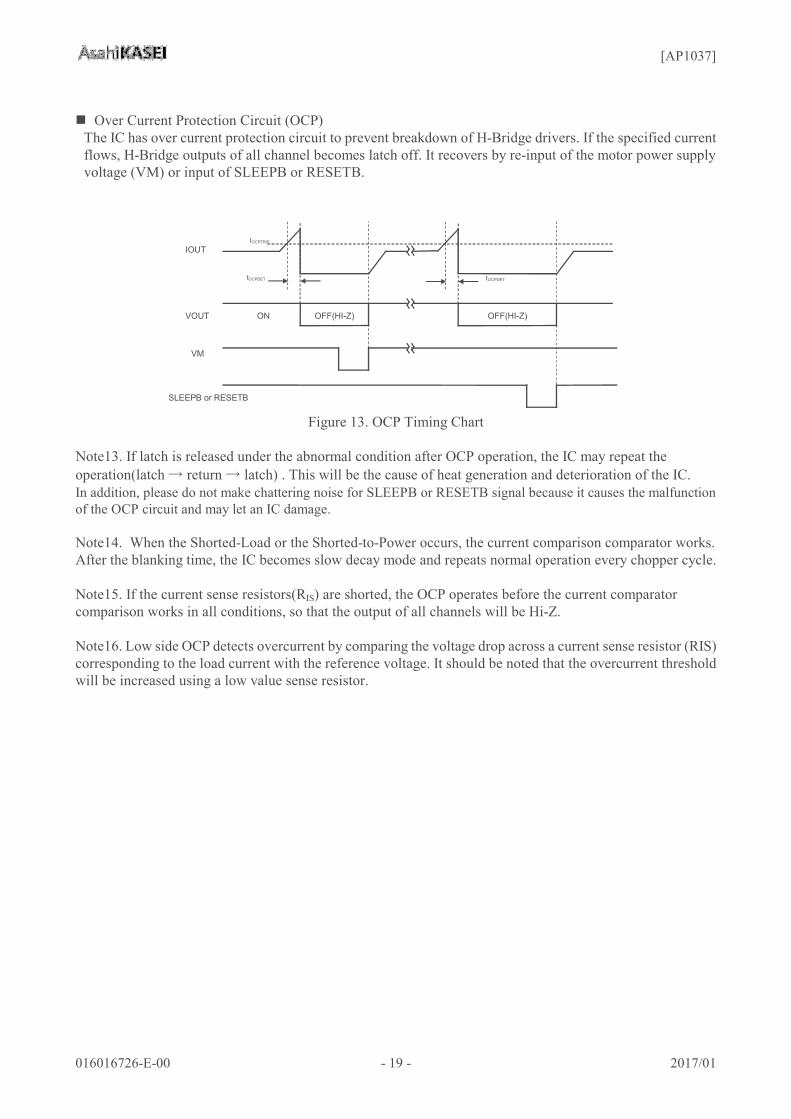
Over Current Protection Circuit (OCP) The IC has over current protection circuit to prevent breakdown of H-Bridge drivers. If the specified current flows, H-Bridge outputs of all channel becomes latch off. It recovers by re-input of the motor power supply voltage (VM) or input of SLEEPB or RESETB.
VOUT ON
IOUTIOCPTRIP
tOCPDET
SLEEPB or RESETB
OFF(HI-Z)OFF(HI-Z)
tOCPDET
VM
Figure 13. OCP Timing Chart
Note13. If latch is released under the abnormal condition after OCP operation, the IC may repeat the operation(latch return latch) . This will be the cause of heat generation and deterioration of the IC. In addition, please do not make chattering noise for SLEEPB or RESETB signal because it causes the malfunctionof the OCP circuit and may let an IC damage.
Note14. When the Shorted-Load or the Shorted-to-Power occurs, the current comparison comparator works. After the blanking time, the IC becomes slow decay mode and repeats normal operation every chopper cycle.
Note15. If the current sense resistors(RIS) are shorted, the OCP operates before the current comparator comparison works in all conditions, so that the output of all channels will be Hi-Z.
Note16. Low side OCP detects overcurrent by comparing the voltage drop across a current sense resistor (RIS)corresponding to the load current with the reference voltage. It should be noted that the overcurrent threshold will be increased using a low value sense resistor.

[AP1037]
016016726-E-00 - 20 - 2017/01
11. Recommended External CircuitRecommended External Circuit
VDCCVDC
VREF
FS
RR1
RR2
STEP RESET_BMODE1
MODE2ENABLE_B
SLEEP_B
MCU
VM1 VM2
CVM1 CVM2CVMVM
VG
CVG
CH CL
CHL
M
OUT1A
OUT1B
OUT2A
OUT2B
RIS1
RIS2
GND
Exposed Pad
AP1034
IS1
IS2
DIR
Figure 14. Recommended External Circuit
Table 12. Recommended External Components Items typ UnitCVM 100 F Electrolytic Capacitor
CVM1 0.22 F Ceramic CapacitorCVM2 0.22 F Ceramic CapacitorCHL 0.01 F Ceramic CapacitorCVG 0.1 F Ceramic Capacitor
CVDC 0.22 F Ceramic CapacitorRIS1 0.24 At 1.25[A]setting (@VREF=2.38V)RIS2 0.24 At 1.25[A]setting (@VREF=2.38V)RR1 33 At VREF=2.38V setting (@VC=5.0V)RR2 30 At VREF=2.38V setting (@VC=5.0V)
Note 17. Above values are examples. Please choose appropriate external components for your system board. Note 18. Capacitance of CVM and CVC should be determined in consideration of the load current profile, the load capacitance, the line resistance and etc. of the actual system board.
AP1037
[AP1037]
016016726-E-00 - 21 - 2017/01
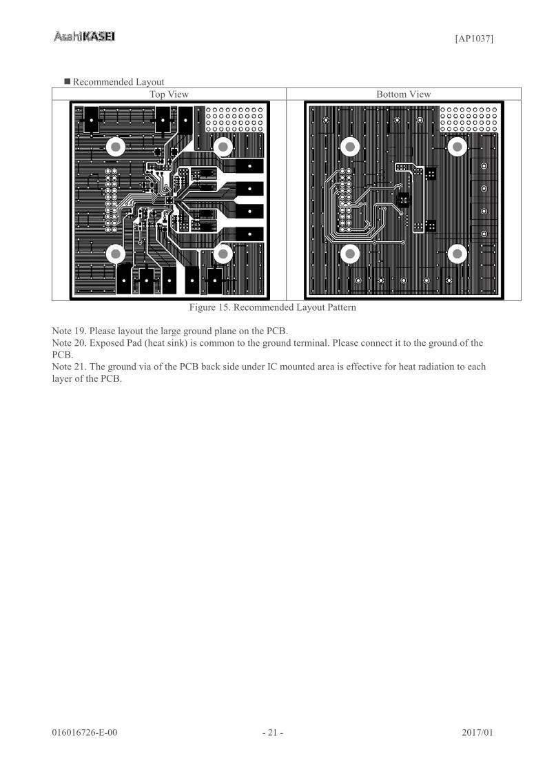
Recommended Layout Top View Bottom View
Figure 15. Recommended Layout Pattern
Note 19. Please layout the large ground plane on the PCB.Note 20. Exposed Pad (heat sink) is common to the ground terminal. Please connect it to the ground of the PCB. Note 21. The ground via of the PCB back side under IC mounted area is effective for heat radiation to each layer of the PCB.
[AP1037]
016016726-E-00 - 22 - 2017/01
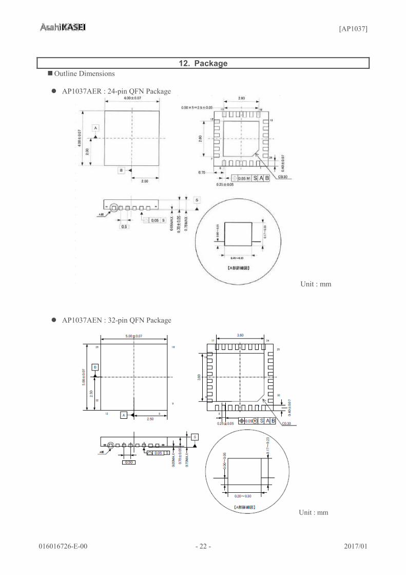
12. PackageOutline Dimensions
AP1037AER : 24-pin QFN Package
Unit : mm
AP1037AEN : 32-pin QFN Package
Unit : mm

[AP1037]
016016726-E-00 - 23 - 2017/01
Recommended Land PatternAP1037AER 24-pin QFN Package
0.2
2.6
3.0
4.6
0.3
Thermal Via
unit: mm
AP1037AEN 32-pin QFN Package
unit: mm
*The most suitable dimensions of the mount pad change by a substrate material, solder paste materials, a soldering method, device precision. It is therefore recommended that customers contact the actual design should be optimized according to the situation.

[AP1037]
016016726-E-00 - 24 - 2017/01
Marking AP1037AER
YWWAA
(1) 1pin Indication(2) Market No.(3) Year code (last 1 digit)(4) Week code(5) Management code(1)
1037AR
(3)
(2)
(4) (5)
AP1037AEN
YWWAA
(1) 1pin Indication(2) Market No.(3) Year code (last 1 digit)(4) Week code(5) Management code(1)
1037AN
(3)
(2)
(4) (5)

[AP1037]
016016726-E-00 - 25 - 2017/01
13. Revise History
Date(YY/MM/DD) Revision Page Contents
17/02/02 00 - First Edition
[AP1037]
016016726-E-00 - 26 - 2017/01
IMPORTANT NOTICE
0. Asahi Kasei Microdevices Corporation (“AKM”) reserves the right to make changes to the information contained in this document without notice. When you consider any use or application of AKM product stipulated in this document (“Product”), please make inquiries the sales office of AKM or authorized distributors as to current status of the Products.
1. All information included in this document are provided only to illustrate the operation and application examples of AKM Products. AKM neither makes warranties or representations with respect to the accuracy or completeness of the information contained in this document nor grants any license to any intellectual property rights or any other rights of AKM or any third party with respect to the information in this document. You are fully responsible for use of such information contained in this document in your product design or applications. AKM ASSUMES NO LIABILITY FOR ANY LOSSES INCURRED BY YOU OR THIRD PARTIES ARISING FROM THE USE OF SUCH INFORMATION IN YOUR PRODUCT DESIGN OR APPLICATIONS.
2. The Product is neither intended nor warranted for use in equipment or systems that require extraordinarily high levels of quality and/or reliability and/or a malfunction or failure of which may cause loss of human life, bodily injury, serious property damage or serious public impact, including but not limited to, equipment used in nuclear facilities, equipment used in the aerospace industry, medical equipment, equipment used for automobiles, trains, ships and other transportation, traffic signaling equipment, equipment used to control combustions or explosions, safety devices, elevators and escalators, devices related to electric power, and equipment used in finance-related fields. Do not use Product for the above use unless specifically agreed by AKM in writing.
3. Though AKM works continually to improve the Product’s quality and reliability, you are responsible for complying with safety standards and for providing adequate designs and safeguards for your hardware, software and systems which minimize risk and avoid situations in which a malfunction or failure of the Product could cause loss of human life, bodily injury or damage to property, including data loss or corruption.
4. Do not use or otherwise make available the Product or related technology or any information contained in this document for any military purposes, including without limitation, for the design, development, use, stockpiling or manufacturing of nuclear, chemical, or biological weapons or missile technology products (mass destruction weapons). When exporting the Products or related technology or any information contained in this document, you should comply with the applicable export control laws and regulations and follow the procedures required by such laws and regulations.The Products and related technology may not be used for or incorporated into any products or systems whose manufacture, use, or sale is prohibited under any applicable domestic or foreign laws or regulations.
5. Please contact AKM sales representative for details as to environmental matters such as the RoHS compatibility of the Product. Please use the Product in compliance with all applicable laws and regulations that regulate the inclusion or use of controlled substances, including without limitation, the EU RoHS Directive. AKM assumes no liability for damages or losses occurring as a result ofnoncompliance with applicable laws and regulations.
6. Resale of the Product with provisions different from the statement and/or technical features set forth in this document shall immediately void any warranty granted by AKM for the Product and shall not create or extend in any manner whatsoever, any liability of AKM.
7. This document may not be reproduced or duplicated, in any form, in whole or in part, without prior written consent of AKM.