Embed Size (px)
Citation preview
Stepping into next-generation architectures for multi-camera operations in automobilesA highly integrated approach to achieve extended synchronization and advanced high-dynamic range image quality to enable automotive surround view and camera monitoring systems
Thorsten LorenzenAutomotive Systems
Mayank ManglaAutomotive Processors
Shashank DabralAutomotive Processors
Texas Instruments
Stepping into next-generation architectures for 2 June 2017multi-camera operations in automobiles
Introduction
Today’s surround view systems may have four cameras or more to observe and analyze
the scene around an automobile. Typically, at least four camera streams will be stitched
together in a 2D or 3D display for the best driver experience.
Camera monitor systems (CMS), which are now replacing as many as six mirrors
on trucks, may require two cameras on the driver’s side and two cameras on
the passenger side, rendering the video streams to create a very wide view. Both
architectures interconnect megapixel image sensors with one central application
processor by bridging the long distance over a single coax cable. This requires that
the video streams to arrive fully synchronized. While current generation systems are
1 megapixel (MP) in resolution, but next-generation systems demand image resolutions of
2 MP and more at up to 60 frames per second frame (fps) rate. Light-emitting diode (LED)
flickering caused by the pulse-width modulation (PWM) of LED lights in traffic signs and
cars is another problem. In addition, the market demands higher dynamic range (HDR)
imaging suitable for extreme lighting conditions, requiring additional pixel processing.
Video stream transmission systems need to feature central clock distribution; video
synchronization, back-channel communication and power over coax (PoC) capabilities.
In order to achieve all this, highly integrated solutions feature chipsets of multiple
FPD-Link serializers combined with a single FPD-Link deserializer hub.
This paper discusses how to fulfill market demands for HDR, LED flicker mitigation,
low-light performance and advanced image quality.
Image sensor technology
Today’s complementary metal-oxide semiconductor
(CMOS) color imagers provide 1 MP, 2 MP or
more on an image sensor chip for automotive
applications. They record highly detailed images,
providing video streams up to 60 fps. HDR sensors
usually output multiple images for the same frame
with different exposure/gain values. There are many
sensor architectures like split-pixel, digital overlap
and staggered HDR. Those sensor architectures
require significantly higher computational
performance in image signal processing (ISP) units
to process HDR images. Currently, image sensor
manufacturers are moving the ISP block off the
imager chip to limit power dissipation and heat
generation in the camera and help increase image
quality. In addition, this helps counter for the larger
technology node that the imagers are fabricated in.
So, ISPs will be integrated into vision processors
(SoC) or remain as standalone devices. With
advanced HDR capabilities, ISPs can even process
multiple camera streams concurrently, reducing the
Stepping into next-generation architectures for 3 June 2017multi-camera operations in automobiles
number of ISP devices needed in the system. To
accomplish this, camera streams need additional
indication for channel separation otherwise, the
video streams may get mixed up in the system path.
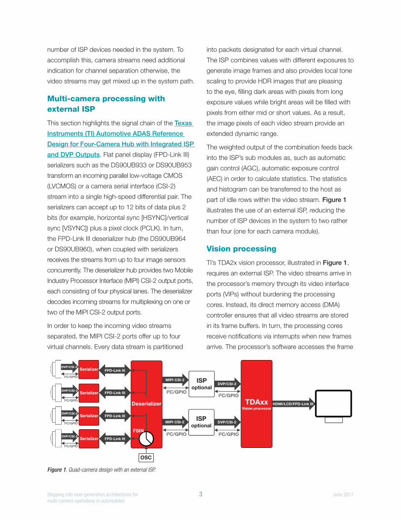
Multi-camera processing with external ISP
This section highlights the signal chain of the Texas
Instruments (TI) Automotive ADAS Reference
Design for Four-Camera Hub with Integrated ISP
and DVP Outputs. Flat panel display (FPD-Link III)
serializers such as the DS90UB933 or DS90UB953
transform an incoming parallel low-voltage CMOS
(LVCMOS) or a camera serial interface (CSI-2)
stream into a single high-speed differential pair. The
serializers can accept up to 12 bits of data plus 2
bits (for example, horizontal sync [HSYNC]/vertical
sync [VSYNC]) plus a pixel clock (PCLK). In turn,
the FPD-Link III deserializer hub (the DS90UB964
or DS90UB960), when coupled with serializers
receives the streams from up to four image sensors
concurrently. The deserializer hub provides two Mobile
Industry Processor Interface (MIPI) CSI-2 output ports,
each consisting of four physical lanes. The deserializer
decodes incoming streams for multiplexing on one or
two of the MIPI CSI-2 output ports.
In order to keep the incoming video streams
separated, the MIPI CSI-2 ports offer up to four
virtual channels. Every data stream is partitioned
into packets designated for each virtual channel.
The ISP combines values with different exposures to
generate image frames and also provides local tone
scaling to provide HDR images that are pleasing
to the eye, filling dark areas with pixels from long
exposure values while bright areas will be filled with
pixels from either mid or short values. As a result,
the image pixels of each video stream provide an
extended dynamic range.
The weighted output of the combination feeds back
into the ISP’s sub modules as, such as automatic
gain control (AGC), automatic exposure control
(AEC) in order to calculate statistics. The statistics
and histogram can be transferred to the host as
part of idle rows within the video stream. Figure 1
illustrates the use of an external ISP, reducing the
number of ISP devices in the system to two rather
than four (one for each camera module).
Vision processing
TI’s TDA2x vision processor, illustrated in Figure 1,
requires an external ISP. The video streams arrive in
the processor’s memory through its video interface
ports (VIPs) without burdening the processing
cores. Instead, its direct memory access (DMA)
controller ensures that all video streams are stored
in its frame buffers. In turn, the processing cores
receive notifications via interrupts when new frames
arrive. The processor’s software accesses the frame
OSC
I2C/GPIO
DVP/CSI-2Serializer
I2C/GPIO
DVP/CSI-2Serializer
I2C/GPIO
DVP/CSI-2Serializer
I2C/GPIO
DVP/CSI-2Serializer
FPD-Link III
I2C/GPIO
MIPI CSI-2
ISPoptional
FPD-Link III
FPD-Link III
FPD-Link III
I2C/GPIO
MIPI CSI-2
TDAxxVision processor
I2C/GPIO
I2C/GPIO
DVP/CSI-2ISP
optional
DVP/CSI-2
HDMI/LCD/FPD-Link III
FSIN
Deserializer
Figure 1
Figure 1. Quad-camera design with an external ISP.
Stepping into next-generation architectures for 4 June 2017multi-camera operations in automobiles
buffers as needed to process the video data. For
monitoring purposes multiple video streams can
be stitched to form up a rendered single “multi-
channel” video stream. TDAx processors offer
several options to output video streams onto a
monitoring back end. Beside HDMI and RGB LCDs
even transfers over FPD-Link III serializers (e.g.,
DS90UB925) are possible. Those will bridge longer
distances to the display side.
Next-generation TDAx processors integrate the ISP
on-chip pushing chip integration to a higher level.
This results in reduced cost, better photometric
alignment and lower power consumption.
Achieving video stream synchronization
Camera synchronization can become a challenge.
The processing time of each camera can vary due
to component tolerances or even conditions in the
visual scene being processed, necessitating the
introduction of time stamp mechanisms in software
to overcome the problem. However, additional
software would further utilize the vision processor.
As a solution, we will discuss four hardware features
that ensure frames from all video streams arrive in
the vision processor at same time and no additional
software engagement would be required.
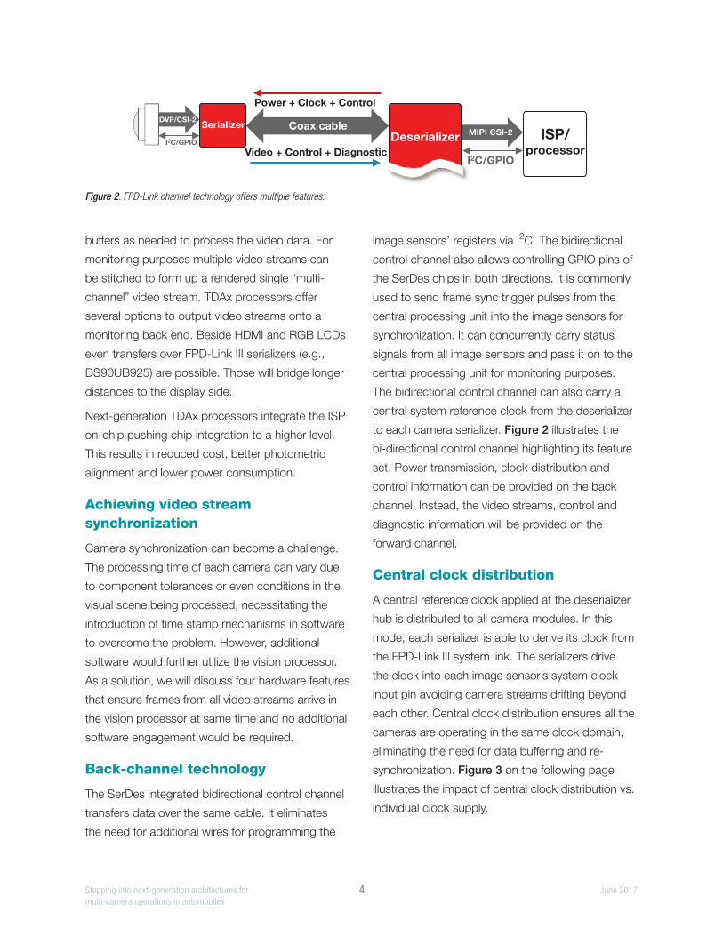
Back-channel technology
The SerDes integrated bidirectional control channel
transfers data over the same cable. It eliminates
the need for additional wires for programming the
image sensors’ registers via I2C. The bidirectional
control channel also allows controlling GPIO pins of
the SerDes chips in both directions. It is commonly
used to send frame sync trigger pulses from the
central processing unit into the image sensors for
synchronization. It can concurrently carry status
signals from all image sensors and pass it on to the
central processing unit for monitoring purposes.
The bidirectional control channel can also carry a
central system reference clock from the deserializer
to each camera serializer. Figure 2 illustrates the
bi-directional control channel highlighting its feature
set. Power transmission, clock distribution and
control information can be provided on the back
channel. Instead, the video streams, control and
diagnostic information will be provided on the
forward channel.
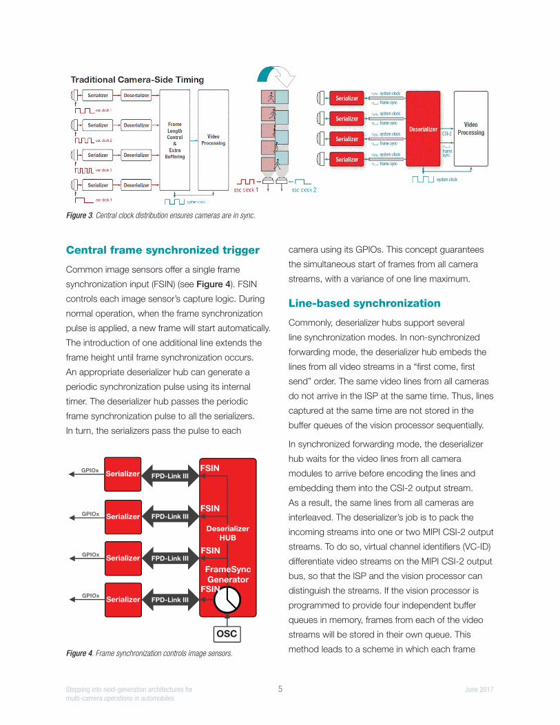
Central clock distribution
A central reference clock applied at the deserializer
hub is distributed to all camera modules. In this
mode, each serializer is able to derive its clock from
the FPD-Link III system link. The serializers drive
the clock into each image sensor’s system clock
input pin avoiding camera streams drifting beyond
each other. Central clock distribution ensures all the
cameras are operating in the same clock domain,
eliminating the need for data buffering and re-
synchronization. Figure 3 on the following page
illustrates the impact of central clock distribution vs.
individual clock supply.
I2C/GPIO
DVP/CSI-2 Serializer Coax cable
ISP/ processor
I2C/GPIO
MIPI CSI-2 Deserializer
Power + Clock + Control
Video + Control + Diagnostic
Figure 2
Figure 2. FPD-Link channel technology offers multiple features.
Stepping into next-generation architectures for 5 June 2017multi-camera operations in automobiles
Central frame synchronized trigger
Common image sensors offer a single frame
synchronization input (FSIN) (see Figure 4). FSIN
controls each image sensor’s capture logic. During
normal operation, when the frame synchronization
pulse is applied, a new frame will start automatically.
The introduction of one additional line extends the
frame height until frame synchronization occurs.
An appropriate deserializer hub can generate a
periodic synchronization pulse using its internal
timer. The deserializer hub passes the periodic
frame synchronization pulse to all the serializers.
In turn, the serializers pass the pulse to each
camera using its GPIOs. This concept guarantees
the simultaneous start of frames from all camera
streams, with a variance of one line maximum.
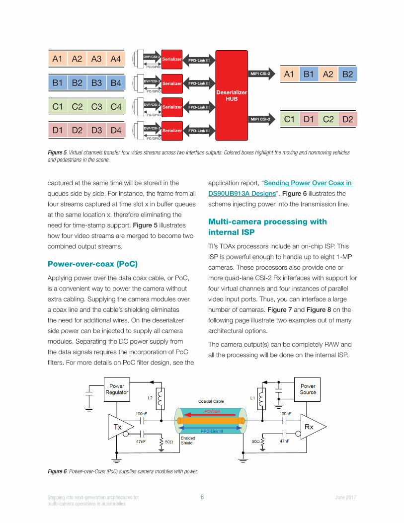
Line-based synchronization
Commonly, deserializer hubs support several
line synchronization modes. In non-synchronized
forwarding mode, the deserializer hub embeds the
lines from all video streams in a “first come, first
send” order. The same video lines from all cameras
do not arrive in the ISP at the same time. Thus, lines
captured at the same time are not stored in the
buffer queues of the vision processor sequentially.
In synchronized forwarding mode, the deserializer
hub waits for the video lines from all camera
modules to arrive before encoding the lines and
embedding them into the CSI-2 output stream.
As a result, the same lines from all cameras are
interleaved. The deserializer’s job is to pack the
incoming streams into one or two MIPI CSI-2 output
streams. To do so, virtual channel identifiers (VC-ID)
differentiate video streams on the MIPI CSI-2 output
bus, so that the ISP and the vision processor can
distinguish the streams. If the vision processor is
programmed to provide four independent buffer
queues in memory, frames from each of the video
streams will be stored in their own queue. This
method leads to a scheme in which each frame
OSC
Serializer
Serializer
Serializer
Serializer
FPD-Link III
FPD-Link III
FPD-Link III
FPD-Link III
FSINGPIOx
GPIOx
GPIOx
GPIOx
FSIN
FSIN
FSIN
Figure 4
DeserializerHUB
FrameSyncGenerator
Figure 4. Frame synchronization controls image sensors.
Figure 3. Central clock distribution ensures cameras are in sync.
Stepping into next-generation architectures for 6 June 2017multi-camera operations in automobiles
Figure 5. Virtual channels transfer four video streams across two interface outputs. Colored boxes highlight the moving and nonmoving vehicles and pedestrians in the scene.
captured at the same time will be stored in the
queues side by side. For instance, the frame from all
four streams captured at time slot x in buffer queues
at the same location x, therefore eliminating the
need for time-stamp support. Figure 5 illustrates
how four video streams are merged to become two
combined output streams.
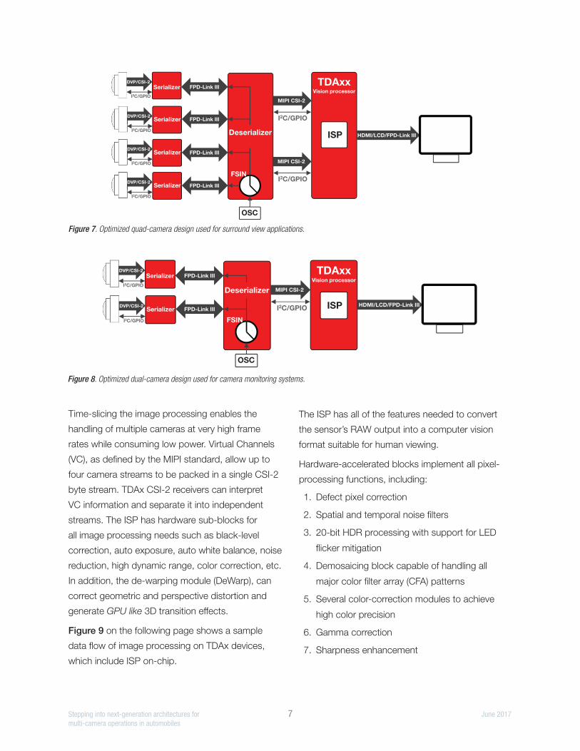
Power-over-coax (PoC)
Applying power over the data coax cable, or PoC,
is a convenient way to power the camera without
extra cabling. Supplying the camera modules over
a coax line and the cable’s shielding eliminates
the need for additional wires. On the deserializer
side power can be injected to supply all camera
modules. Separating the DC power supply from
the data signals requires the incorporation of PoC
filters. For more details on PoC filter design, see the
application report, “Sending Power Over Coax in
DS90UB913A Designs”. Figure 6 illustrates the
scheme injecting power into the transmission line.
Multi-camera processing with internal ISP
TI’s TDAx processors include an on-chip ISP. This
ISP is powerful enough to handle up to eight 1-MP
cameras. These processors also provide one or
more quad-lane CSI-2 Rx interfaces with support for
four virtual channels and four instances of parallel
video input ports. Thus, you can interface a large
number of cameras. Figure 7 and Figure 8 on the
following page illustrate two examples out of many
architectural options.
The camera output(s) can be completely RAW and
all the processing will be done on the internal ISP.
Figure 6. Power-over-Coax (PoC) supplies camera modules with power.
I2C/GPIO
DVP/CSI-2Serializer
I2C/GPIO
DVP/CSI-2Serializer
I2C/GPIO
DVP/CSI-2Serializer
I2C/GPIO
DVP/CSI-2Serializer
FPD-Link III
FPD-Link III
FPD-Link III
FPD-Link III
DeserializerHUB
A1 A2 A3 A4
B1 B2 B3 B4
C1 C2 C3 C4
D1 D2 D3 D4
A1 B1 A2 B2
C1 D1 C2 D2
MIPI CSI-2
MIPI CSI-2
Figure 5
Stepping into next-generation architectures for 7 June 2017multi-camera operations in automobiles
Time-slicing the image processing enables the
handling of multiple cameras at very high frame
rates while consuming low power. Virtual Channels
(VC), as defined by the MIPI standard, allow up to
four camera streams to be packed in a single CSI-2
byte stream. TDAx CSI-2 receivers can interpret
VC information and separate it into independent
streams. The ISP has hardware sub-blocks for
all image processing needs such as black-level
correction, auto exposure, auto white balance, noise
reduction, high dynamic range, color correction, etc.
In addition, the de-warping module (DeWarp), can
correct geometric and perspective distortion and
generate GPU like 3D transition effects.
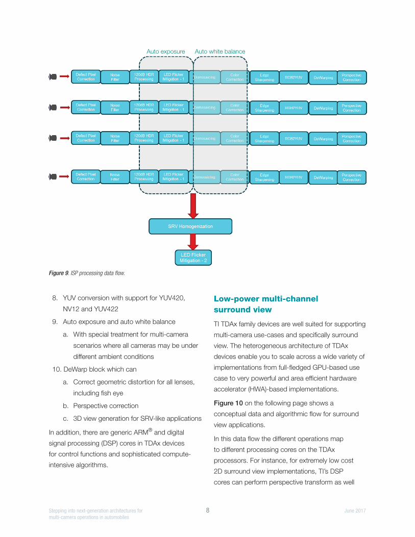
Figure 9 on the following page shows a sample
data flow of image processing on TDAx devices,
which include ISP on-chip.
The ISP has all of the features needed to convert
the sensor’s RAW output into a computer vision
format suitable for human viewing.
Hardware-accelerated blocks implement all pixel-
processing functions, including:
1. Defect pixel correction
2. Spatial and temporal noise filters
3. 20-bit HDR processing with support for LED
flicker mitigation
4. Demosaicing block capable of handling all
major color filter array (CFA) patterns
5. Several color-correction modules to achieve
high color precision
6. Gamma correction
7. Sharpness enhancement
Figure 7. Optimized quad-camera design used for surround view applications.
OSC
I2C/GPIO
DVP/CSI-2
I2C/GPIO
DVP/CSI-2Serializer
I2C/GPIO
DVP/CSI-2Serializer
I2C/GPIO
DVP/CSI-2Serializer
FPD-Link III
I2C/GPIO
MIPI CSI-2
FPD-Link III
FPD-Link III
FPD-Link III
I2C/GPIO
MIPI CSI-2
TDAxxVision processor
FSIN
Deserializer
Serializer
ISP HDMI/LCD/FPD-Link III
Figure 7
Figure 8. Optimized dual-camera design used for camera monitoring systems.
OSC
I2C/GPIO
DVP/CSI-2
I2C/GPIO
DVP/CSI-2Serializer
FPD-Link III
FPD-Link III I2C/GPIO
MIPI CSI-2
TDAxxVision processor
FSIN
Deserializer
Serializer
ISP HDMI/LCD/FPD-Link III
Figure 8
Stepping into next-generation architectures for 8 June 2017multi-camera operations in automobiles
8. YUV conversion with support for YUV420,
NV12 and YUV422
9. Auto exposure and auto white balance
a. With special treatment for multi-camera
scenarios where all cameras may be under
different ambient conditions
10. DeWarp block which can
a. Correct geometric distortion for all lenses,
including fish eye
b. Perspective correction
c. 3D view generation for SRV-like applications
In addition, there are generic ARM® and digital
signal processing (DSP) cores in TDAx devices
for control functions and sophisticated compute-
intensive algorithms.
Low-power multi-channel surround view
TI TDAx family devices are well suited for supporting
multi-camera use-cases and specifically surround
view. The heterogeneous architecture of TDAx
devices enable you to scale across a wide variety of
implementations from full-fledged GPU-based use
case to very powerful and area efficient hardware
accelerator (HWA)-based implementations.
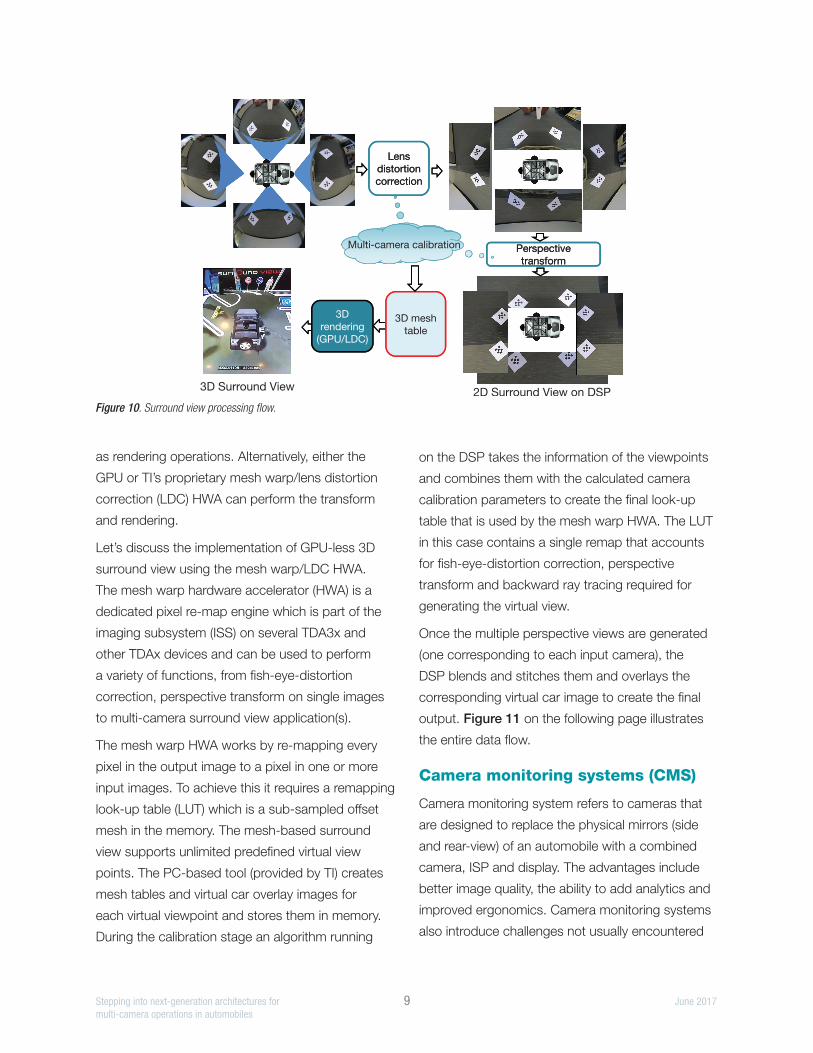
Figure 10 on the following page shows a
conceptual data and algorithmic flow for surround
view applications.
In this data flow the different operations map
to different processing cores on the TDAx
processors. For instance, for extremely low cost
2D surround view implementations, TI’s DSP
cores can perform perspective transform as well
Figure 9. ISP processing data flow.
Auto exposure Auto white balance
Stepping into next-generation architectures for 9 June 2017multi-camera operations in automobiles
as rendering operations. Alternatively, either the
GPU or TI’s proprietary mesh warp/lens distortion
correction (LDC) HWA can perform the transform
and rendering.
Let’s discuss the implementation of GPU-less 3D
surround view using the mesh warp/LDC HWA.
The mesh warp hardware accelerator (HWA) is a
dedicated pixel re-map engine which is part of the
imaging subsystem (ISS) on several TDA3x and
other TDAx devices and can be used to perform
a variety of functions, from fish-eye-distortion
correction, perspective transform on single images
to multi-camera surround view application(s).
The mesh warp HWA works by re-mapping every
pixel in the output image to a pixel in one or more
input images. To achieve this it requires a remapping
look-up table (LUT) which is a sub-sampled offset
mesh in the memory. The mesh-based surround
view supports unlimited predefined virtual view
points. The PC-based tool (provided by TI) creates
mesh tables and virtual car overlay images for
each virtual viewpoint and stores them in memory.
During the calibration stage an algorithm running
on the DSP takes the information of the viewpoints
and combines them with the calculated camera
calibration parameters to create the final look-up
table that is used by the mesh warp HWA. The LUT
in this case contains a single remap that accounts
for fish-eye-distortion correction, perspective
transform and backward ray tracing required for
generating the virtual view.
Once the multiple perspective views are generated
(one corresponding to each input camera), the
DSP blends and stitches them and overlays the
corresponding virtual car image to create the final
output. Figure 11 on the following page illustrates
the entire data flow.
Camera monitoring systems (CMS)
Camera monitoring system refers to cameras that
are designed to replace the physical mirrors (side
and rear-view) of an automobile with a combined
camera, ISP and display. The advantages include
better image quality, the ability to add analytics and
improved ergonomics. Camera monitoring systems
also introduce challenges not usually encountered
Figure 10. Surround view processing flow.
How to Generate Surround View
Lens distortion correction
Lens distortion correction
Perspective transform
Perspective transform
Multi-camera calibration
3D mesh table
3D rendering
(GPU/LDC)
2D Surround View on DSP3D Surround View
Stepping into next-generation architectures for 10 June 2017multi-camera operations in automobiles
in other categories of imaging applications. Let’s
describe some of these challenges and the solution
implemented on the TI TDAx processor family.
Typical requirements of a CMS system include:
Higher frame rate and low light performance
International Organization for Standardization
(ISO) 16505 requires 15–30 fps, but higher
frame rates are recommended for a high-quality
camera monitoring solution. To get better low-
light performance, variable frame rate is desired
depending on lighting conditions and driving speed.
TDAx ISPs can process high-resolution images at
very high frame rates because of a fully hardware-
accelerated implementation. Variable frame rate
is achieved by adding a feedback loop between
the hardware 3A engine (H3A), auto exposure (AE)
algorithm and sensor driver achieves a variable
frame rate. The H3A generates scene statistics
which are used by the AE algorithm to estimate the
average brightness of the scene. The result of the
AE estimation is fed back to the sensor driver to
account for increased or decreased exposures and
gain. Furthermore, the result of the AE algorithm
also sets sensor timing registers to adjust the frame
rate allowing longer time in low light to achieve
higher signal-to-noise ratio (SNR).
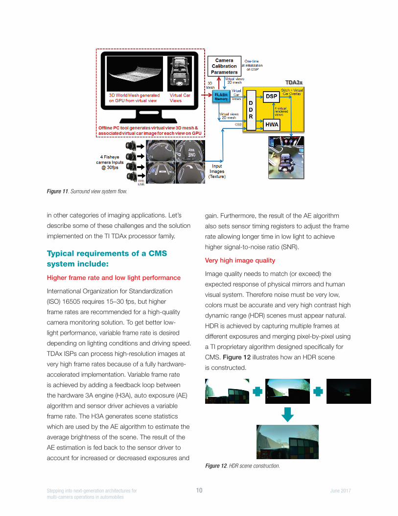
Very high image quality
Image quality needs to match (or exceed) the
expected response of physical mirrors and human
visual system. Therefore noise must be very low,
colors must be accurate and very high contrast high
dynamic range (HDR) scenes must appear natural.
HDR is achieved by capturing multiple frames at
different exposures and merging pixel-by-pixel using
a TI proprietary algorithm designed specifically for
CMS. Figure 12 illustrates how an HDR scene
is constructed.
Figure 12. HDR scene construction.
TDA3x 3D SRV – Data Flow
Figure 11. Surround view system flow.
Stepping into next-generation architectures for 11 June 2017multi-camera operations in automobiles
LED flicker mitigation
LEDs have revolutionized the lighting industry
including automotive headlights and road signs.
While this is a welcome development, it poses
a challenge for CMOS camera sensors. LED
illumination is based on PWM, where light is emitted
only during the ON cycle. CMOS sensors use
a rolling shutter mechanism and are not able to
capture the LED signal entirely in every consecutive
frame. This leads to a flicker effect where the LEDs
are seen as OFF in some frames and ON in others.
This problem is compounded by wide dynamic
range imaging since the rolling shutter window
is set to a very small time to capture highlights in
the scene. TI’s TDAx CMS solution addresses this
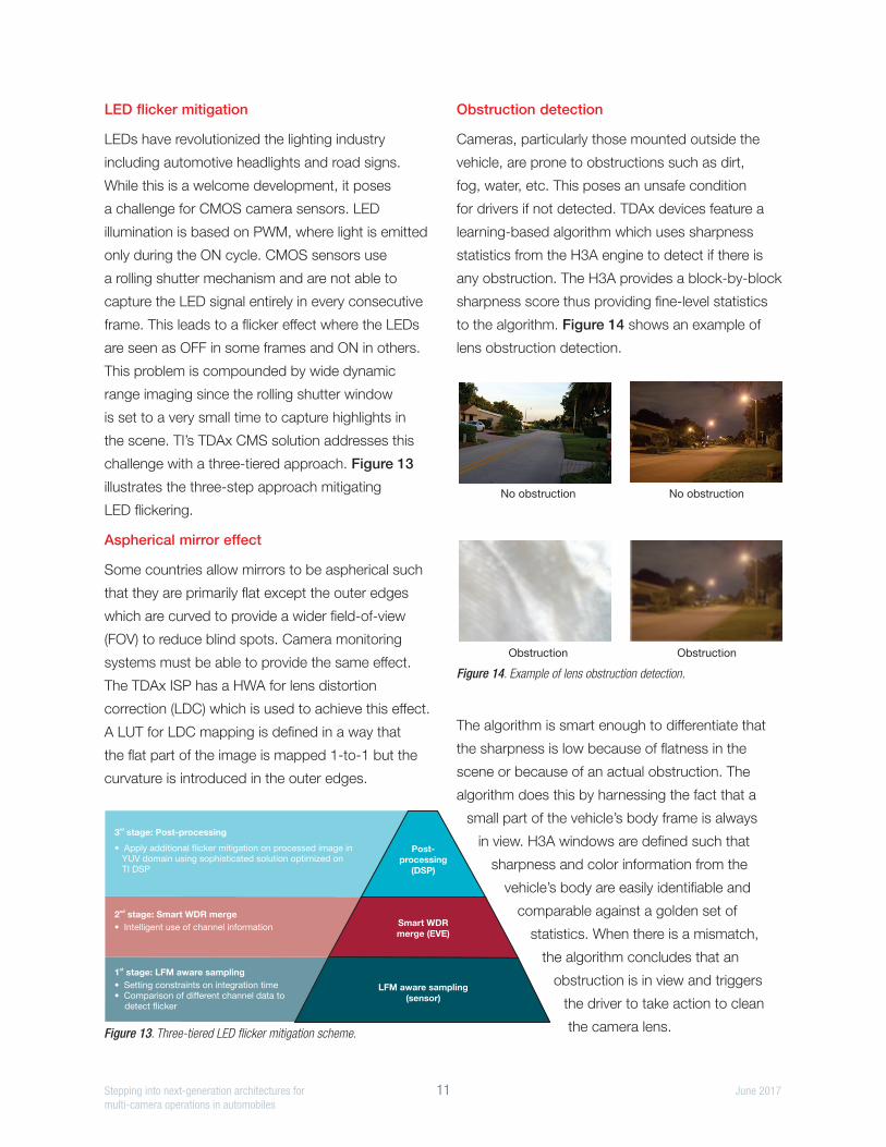
challenge with a three-tiered approach. Figure 13
illustrates the three-step approach mitigating
LED flickering.
Aspherical mirror effect
Some countries allow mirrors to be aspherical such
that they are primarily flat except the outer edges
which are curved to provide a wider field-of-view
(FOV) to reduce blind spots. Camera monitoring
systems must be able to provide the same effect.
The TDAx ISP has a HWA for lens distortion
correction (LDC) which is used to achieve this effect.
A LUT for LDC mapping is defined in a way that
the flat part of the image is mapped 1-to-1 but the
curvature is introduced in the outer edges.
Obstruction detection
Cameras, particularly those mounted outside the
vehicle, are prone to obstructions such as dirt,
fog, water, etc. This poses an unsafe condition
for drivers if not detected. TDAx devices feature a
learning-based algorithm which uses sharpness
statistics from the H3A engine to detect if there is
any obstruction. The H3A provides a block-by-block
sharpness score thus providing fine-level statistics
to the algorithm. Figure 14 shows an example of
lens obstruction detection.
The algorithm is smart enough to differentiate that
the sharpness is low because of flatness in the
scene or because of an actual obstruction. The
algorithm does this by harnessing the fact that a
small part of the vehicle’s body frame is always
in view. H3A windows are defined such that
sharpness and color information from the
vehicle’s body are easily identifiable and
comparable against a golden set of
statistics. When there is a mismatch,
the algorithm concludes that an
obstruction is in view and triggers
the driver to take action to clean
the camera lens.Figure 13. Three-tiered LED flicker mitigation scheme.
Post-
processing
(DSP)
Smart WDR
merge (EVE)
LFM aware sampling
(sensor)
3 stage: Post-processingrd
2 stage: Smart WDR mergend
1 stage: LFM aware samplingst
• Apply additional flicker mitigation on processed image inYUV domain using sophisticated solution optimized onTI DSP
• Intelligent use of channel information
• Setting constraints on integration time• Comparison of different channel data to
detect flicker
No obstruction
Obstruction Obstruction
No obstruction
Figure 14. Example of lens obstruction detection.
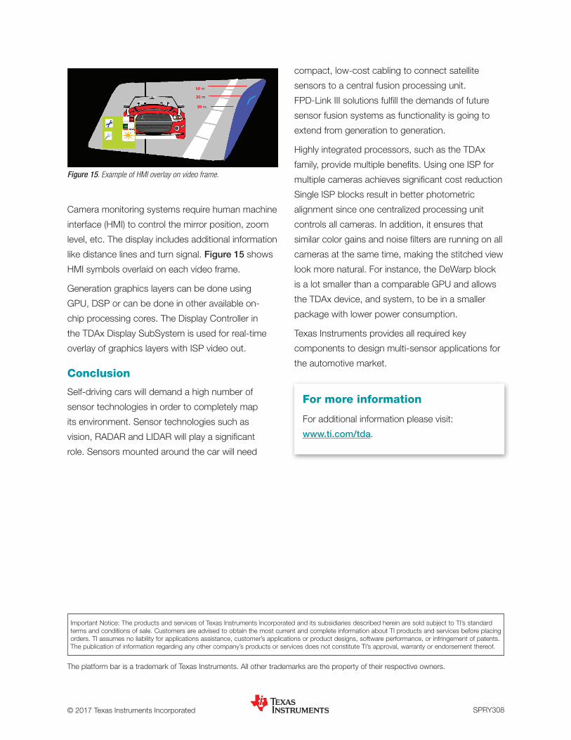
Camera monitoring systems require human machine
interface (HMI) to control the mirror position, zoom
level, etc. The display includes additional information
like distance lines and turn signal. Figure 15 shows
HMI symbols overlaid on each video frame.
Generation graphics layers can be done using
GPU, DSP or can be done in other available on-
chip processing cores. The Display Controller in
the TDAx Display SubSystem is used for real-time
overlay of graphics layers with ISP video out.
Conclusion
Self-driving cars will demand a high number of
sensor technologies in order to completely map
its environment. Sensor technologies such as
vision, RADAR and LIDAR will play a significant
role. Sensors mounted around the car will need
compact, low-cost cabling to connect satellite
sensors to a central fusion processing unit.
FPD-Link III solutions fulfill the demands of future
sensor fusion systems as functionality is going to
extend from generation to generation.
Highly integrated processors, such as the TDAx
family, provide multiple benefits. Using one ISP for
multiple cameras achieves significant cost reduction
Single ISP blocks result in better photometric
alignment since one centralized processing unit
controls all cameras. In addition, it ensures that
similar color gains and noise filters are running on all
cameras at the same time, making the stitched view
look more natural. For instance, the DeWarp block
is a lot smaller than a comparable GPU and allows
the TDAx device, and system, to be in a smaller
package with lower power consumption.
Texas Instruments provides all required key
components to design multi-sensor applications for
the automotive market.
SPRY308© 2017 Texas Instruments Incorporated
Important Notice: The products and services of Texas Instruments Incorporated and its subsidiaries described herein are sold subject to TI’s standard terms and conditions of sale. Customers are advised to obtain the most current and complete information about TI products and services before placing orders. TI assumes no liability for applications assistance, customer’s applications or product designs, software performance, or infringement of patents. The publication of information regarding any other company’s products or services does not constitute TI’s approval, warranty or endorsement thereof.
The platform bar is a trademark of Texas Instruments. All other trademarks are the property of their respective owners.
Figure 15. Example of HMI overlay on video frame.
For more information
For additional information please visit:
www.ti.com/tda.
IMPORTANT NOTICE FOR TI DESIGN INFORMATION AND RESOURCES
Texas Instruments Incorporated (‘TI”) technical, application or other design advice, services or information, including, but not limited to,reference designs and materials relating to evaluation modules, (collectively, “TI Resources”) are intended to assist designers who aredeveloping applications that incorporate TI products; by downloading, accessing or using any particular TI Resource in any way, you(individually or, if you are acting on behalf of a company, your company) agree to use it solely for this purpose and subject to the terms ofthis Notice.TI’s provision of TI Resources does not expand or otherwise alter TI’s applicable published warranties or warranty disclaimers for TIproducts, and no additional obligations or liabilities arise from TI providing such TI Resources. TI reserves the right to make corrections,enhancements, improvements and other changes to its TI Resources.You understand and agree that you remain responsible for using your independent analysis, evaluation and judgment in designing yourapplications and that you have full and exclusive responsibility to assure the safety of your applications and compliance of your applications(and of all TI products used in or for your applications) with all applicable regulations, laws and other applicable requirements. Yourepresent that, with respect to your applications, you have all the necessary expertise to create and implement safeguards that (1)anticipate dangerous consequences of failures, (2) monitor failures and their consequences, and (3) lessen the likelihood of failures thatmight cause harm and take appropriate actions. You agree that prior to using or distributing any applications that include TI products, youwill thoroughly test such applications and the functionality of such TI products as used in such applications. TI has not conducted anytesting other than that specifically described in the published documentation for a particular TI Resource.You are authorized to use, copy and modify any individual TI Resource only in connection with the development of applications that includethe TI product(s) identified in such TI Resource. NO OTHER LICENSE, EXPRESS OR IMPLIED, BY ESTOPPEL OR OTHERWISE TOANY OTHER TI INTELLECTUAL PROPERTY RIGHT, AND NO LICENSE TO ANY TECHNOLOGY OR INTELLECTUAL PROPERTYRIGHT OF TI OR ANY THIRD PARTY IS GRANTED HEREIN, including but not limited to any patent right, copyright, mask work right, orother intellectual property right relating to any combination, machine, or process in which TI products or services are used. Informationregarding or referencing third-party products or services does not constitute a license to use such products or services, or a warranty orendorsement thereof. Use of TI Resources may require a license from a third party under the patents or other intellectual property of thethird party, or a license from TI under the patents or other intellectual property of TI.TI RESOURCES ARE PROVIDED “AS IS” AND WITH ALL FAULTS. TI DISCLAIMS ALL OTHER WARRANTIES ORREPRESENTATIONS, EXPRESS OR IMPLIED, REGARDING TI RESOURCES OR USE THEREOF, INCLUDING BUT NOT LIMITED TOACCURACY OR COMPLETENESS, TITLE, ANY EPIDEMIC FAILURE WARRANTY AND ANY IMPLIED WARRANTIES OFMERCHANTABILITY, FITNESS FOR A PARTICULAR PURPOSE, AND NON-INFRINGEMENT OF ANY THIRD PARTY INTELLECTUALPROPERTY RIGHTS.TI SHALL NOT BE LIABLE FOR AND SHALL NOT DEFEND OR INDEMNIFY YOU AGAINST ANY CLAIM, INCLUDING BUT NOTLIMITED TO ANY INFRINGEMENT CLAIM THAT RELATES TO OR IS BASED ON ANY COMBINATION OF PRODUCTS EVEN IFDESCRIBED IN TI RESOURCES OR OTHERWISE. IN NO EVENT SHALL TI BE LIABLE FOR ANY ACTUAL, DIRECT, SPECIAL,COLLATERAL, INDIRECT, PUNITIVE, INCIDENTAL, CONSEQUENTIAL OR EXEMPLARY DAMAGES IN CONNECTION WITH ORARISING OUT OF TI RESOURCES OR USE THEREOF, AND REGARDLESS OF WHETHER TI HAS BEEN ADVISED OF THEPOSSIBILITY OF SUCH DAMAGES.You agree to fully indemnify TI and its representatives against any damages, costs, losses, and/or liabilities arising out of your non-compliance with the terms and provisions of this Notice.This Notice applies to TI Resources. Additional terms apply to the use and purchase of certain types of materials, TI products and services.These include; without limitation, TI’s standard terms for semiconductor products http://www.ti.com/sc/docs/stdterms.htm), evaluationmodules, and samples (http://www.ti.com/sc/docs/sampterms.htm).
Mailing Address: Texas Instruments, Post Office Box 655303, Dallas, Texas 75265Copyright © 2017, Texas Instruments Incorporated