Embed Size (px)
Citation preview
1/23
www.onsemi.com
Semiconductor Components Industries, LLC, 2014
Nov, 2014 Rev.3
STK551U3xx series
1. Product synopsis
This application handbook is intended to provide practical guidelines for the STK551U3xx series use. The STK551U3xx series is Intelligent Power Module (IPM) based upon ONs Insulated Metal Substrate Technology (IMST) for 3-phase motor drives which contain the main power circuitry and the supporting control circuitry. The key functions are outlined below:
Highly integrated device containing all High Voltage (HV) control from HV-DC to 3-phase outputs in a single small SIP module.
Output stage uses IGBT/FRD technology and implements Under Voltage Protection (UVP) and Over Current Protection (OCP) with a Fault Detection output flag. Internal Boost diodes are provided for high side gate boost drive.
Externally accessible embedded thermistor for substrate temperature measurement.
All control inputs and status outputs are at low voltage levels directly compatible with microcon-trollers.
Single control power supply due to Internal bootstrap circuit for high side pre-driver circuit.
Mounting points are available on SIP package A simplified block diagram of a motor control system is shown in Figure 1.
Figure 1. Motor Control System Block Diagram
Application Note
Intelligent Power Module
STK551U3xx series Application Note
2/23
2. Product description
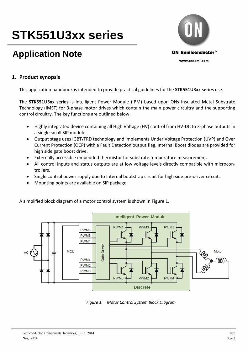
Table1. gives an overview of the available devices, for a detailed description of the packages refer to Chapter 6.
Device STK551U362A-E STK551U392A-E STK551U3A2A-E
Feature single shunt
Package SIP1A – horizontal pins
Voltage (VCEmax.) 600V 600V 600V
Current (Ic) 10A 15A 20A
Peak current (Ic) 20A 30A 40A
Isolation voltage 2000V 2000V 2000V
Shunt resistance 33mΩ 25mΩ 20mΩ
Table 1. Device Overview
+(13)
HIN1(17)
HIN2(18)
HIN3(19)
LIN1(20)
LIN2(21)
LIN3(22)
FAULT(23)
ISO(24)
VDD(25)
VSS(26)
ISD(27)
Shunt-Resistor
Level Shifter
Level Shifter
Level Shifter
Latch time
Logic Logic Logic
Latch time is 18ms to 80ms
( Automatic reset )
VDD-UnderVoltage
Thermistor
-(16)
V,VS2(6)
VB3(1)
W,VS3(2)
VB2(5)
VB1(9)
U.V. U.V. U.V.
U,VS1(10)
Latch
DB DB DB
Over-Current
TH(29)
RCIN(28)
Figure 2. STK551U3xx series equivalent circuits
The high side drive is used with a bootstrap circuit to generate the higher voltage needed for gate drive. The Boost diodes are internal to the part and sourced from VDD (15V). There is an internal level shift cir-cuit for the high side drive signals allowing all control signals to be driven directly from Vss levels common with the control circuit such as the microcontroller without requiring external level shift such as opto iso-lators.
STK551U3xx series Application Note
3/23
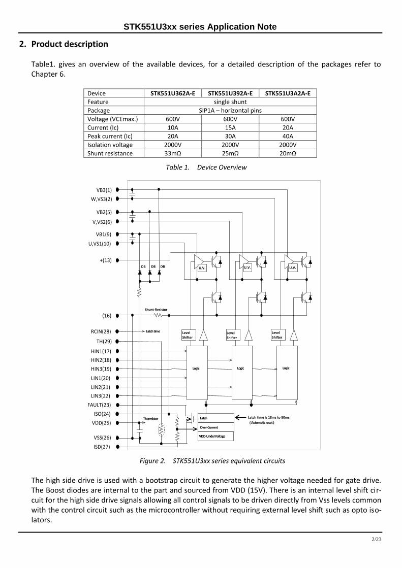
3. Performance test guidelines
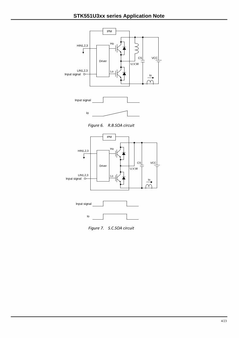
The following Chapter gives performance test method shown in Figures 3 to 7.
3.1. Switching time definition and performance test method
Figure 3. Switching time definition
Figure 4. Evaluation circuit (Inductive load)
Figure 5. Switching loss circuit
IN
Io
VCE
10%
td(ON)
tON tOFF
90%
tr
trr
10%
90%
10%
td(OFF) tf
Ex) Lower side U phase measurement
CS
Vcc
Io
VD1=15V
VD2=15V
VD3=15V
VD4=15V
Input signal
VB1
U,VS1
VB2
V,VS2
VB3
W,VS3
VDD
LIN1
VSS
ISD
+
U,VS1
-
Driver
IPM
HIN1,2,3
LIN1,2,3
Input signal
Ho
Lo
U,V,W
CS VCC
Io
Input signal
Io
STK551U3xx series Application Note
4/23
Figure 6. R.B.SOA circuit
Figure 7. S.C.SOA circuit
Input signal
Io
Driver
IPM
HIN1,2,3
LIN1,2,3
Input signal
Ho
Lo
U,V,W
CS VCC
Io
Input signal
Io
Driver
IPM
HIN1,2,3
LIN1,2,3
Input signal
Ho
Lo
U,V,W
CS VCC
Io
STK551U3xx series Application Note
5/23
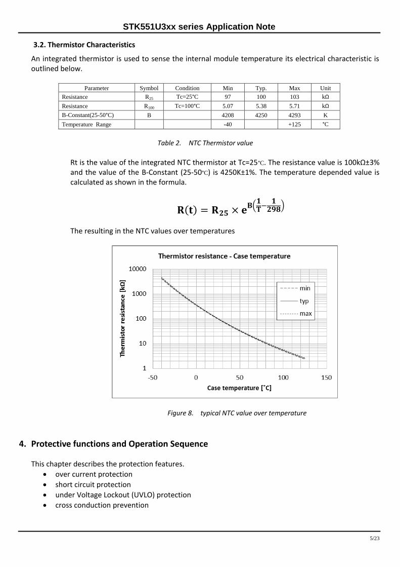
3.2. Thermistor Characteristics
An integrated thermistor is used to sense the internal module temperature its electrical characteristic is outlined below.
Parameter Symbol Condition Min Typ. Max Unit
Resistance R25 Tc=25°C 97 100 103 kΩ
Resistance R100 Tc=100°C 5.07 5.38 5.71 kΩ
B-Constant(25-50°C) B 4208 4250 4293 K
Temperature Range -40 +125 °C
Table 2. NTC Thermistor value
Rt is the value of the integrated NTC thermistor at Tc=25°C. The resistance value is 100kΩ±3%
and the value of the B-Constant (25-50°C) is 4250K±1%. The temperature depended value is calculated as shown in the formula.
𝐑(𝐭) = 𝐑𝟐𝟓 × 𝐞𝐁(
𝟏𝐓−
𝟏𝟐𝟗𝟖)
The resulting in the NTC values over temperatures
Figure 8. typical NTC value over temperature
4. Protective functions and Operation Sequence
This chapter describes the protection features.
over current protection
short circuit protection
under Voltage Lockout (UVLO) protection
cross conduction prevention
STK551U3xx series Application Note
6/23
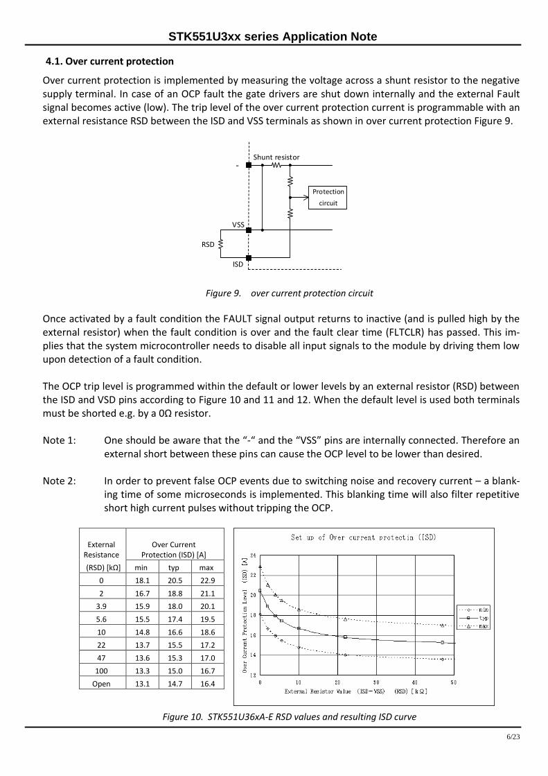
4.1. Over current protection
Over current protection is implemented by measuring the voltage across a shunt resistor to the negative supply terminal. In case of an OCP fault the gate drivers are shut down internally and the external Fault signal becomes active (low). The trip level of the over current protection current is programmable with an external resistance RSD between the ISD and VSS terminals as shown in over current protection Figure 9.
Figure 9. over current protection circuit
Once activated by a fault condition the FAULT signal output returns to inactive (and is pulled high by the external resistor) when the fault condition is over and the fault clear time (FLTCLR) has passed. This im-plies that the system microcontroller needs to disable all input signals to the module by driving them low upon detection of a fault condition. The OCP trip level is programmed within the default or lower levels by an external resistor (RSD) between the ISD and VSD pins according to Figure 10 and 11 and 12. When the default level is used both terminals must be shorted e.g. by a 0Ω resistor. Note 1: One should be aware that the “-“ and the “VSS” pins are internally connected. Therefore an
external short between these pins can cause the OCP level to be lower than desired. Note 2: In order to prevent false OCP events due to switching noise and recovery current – a blank-
ing time of some microseconds is implemented. This blanking time will also filter repetitive short high current pulses without tripping the OCP.
External
Resistance Over Current
Protection (ISD) [A]
(RSD) [kΩ] min typ max
0 18.1 20.5 22.9
2 16.7 18.8 21.1
3.9 15.9 18.0 20.1
5.6 15.5 17.4 19.5
10 14.8 16.6 18.6
22 13.7 15.5 17.2
47 13.6 15.3 17.0
100 13.3 15.0 16.7
Open 13.1 14.7 16.4
Figure 10. STK551U36xA-E RSD values and resulting ISD curve
-
VSS
Protection
circuit
ISD
RSD
Shunt resistor
STK551U3xx series Application Note
7/23
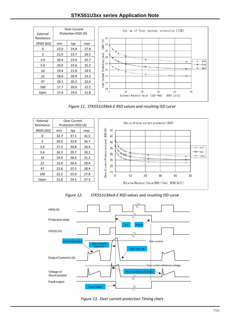
External
Resistance
Over Current Protection (ISD) [A]
(RSD) [kΩ] min typ max
0 22.0 24.8 27.8
2 21.0 23.7 26.5
3.9 20.4 23.0 25.7
5.6 20.0 22.6 25.2
10 19.4 21.8 24.4
22 18.6 20.9 23.3
47 18.1 20.3 22.6
100 17.7 20.0 22.2
Open 17.4 19.6 21.8
Figure 11. STK551U39xA-E RSD values and resulting ISD curve
Figure 12. STK551U3AxA-E RSD values and resulting ISD curve
Figure 13. Over current protection Timing chart
HIN/LIN
Protection state
HVG/LVG
Output Current Ic (A)
Voltage of
Shunt resistor
Fault output
RC circuit time constant
Over current reference voltage
Over current Normal operationOver current
detectionIGBT turn off
Fault output
Set Reset
External Resistance
Over Current Protection (ISD) [A]
(RSD) [kΩ] min typ max
0 32.7 37.1 41.5
2 29.0 32.8 36.7
3.9 27.3 30.8 34.4
5.6 26.3 29.7 33.1
10 24.9 28.0 31.3
22 23.4 26.4 29.4
47 22.6 25.5 28.4
100 22.2 25.0 27.8
Open 21.8 24.5 27.3
STK551U3xx series Application Note
8/23
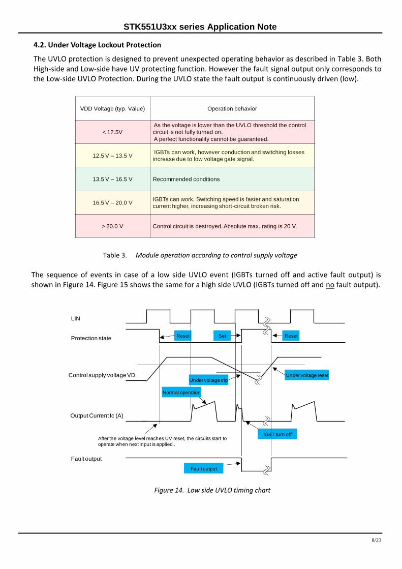
4.2. Under Voltage Lockout Protection
The UVLO protection is designed to prevent unexpected operating behavior as described in Table 3. Both High-side and Low-side have UV protecting function. However the fault signal output only corresponds to the Low-side UVLO Protection. During the UVLO state the fault output is continuously driven (low).
Table 3. Module operation according to control supply voltage
The sequence of events in case of a low side UVLO event (IGBTs turned off and active fault output) is shown in Figure 14. Figure 15 shows the same for a high side UVLO (IGBTs turned off and no fault output).
Figure 14. Low side UVLO timing chart
VDD Voltage (typ. Value) Operation behavior
< 12.5V
As the voltage is lower than the UVLO threshold the control
circuit is not fully turned on.
A perfect functionality cannot be guaranteed.
12.5 V – 13.5 VIGBTs can work, however conduction and switching losses
increase due to low voltage gate signal.
13.5 V – 16.5 V Recommended conditions
16.5 V – 20.0 V IGBTs can work. Switching speed is faster and saturation
current higher, increasing short-circuit broken risk.
> 20.0 V Control circuit is destroyed. Absolute max. rating is 20 V.
LIN
Protection state
Control supply voltage VD
Fault output
After the voltage level reaches UV reset, the circuits start to
operate when next input is applied .
Set Reset
Output Current Ic (A)
IGBT turn off
Normal operation
Fault output
Under voltage trip Under voltage reset
Reset
STK551U3xx series Application Note
9/23
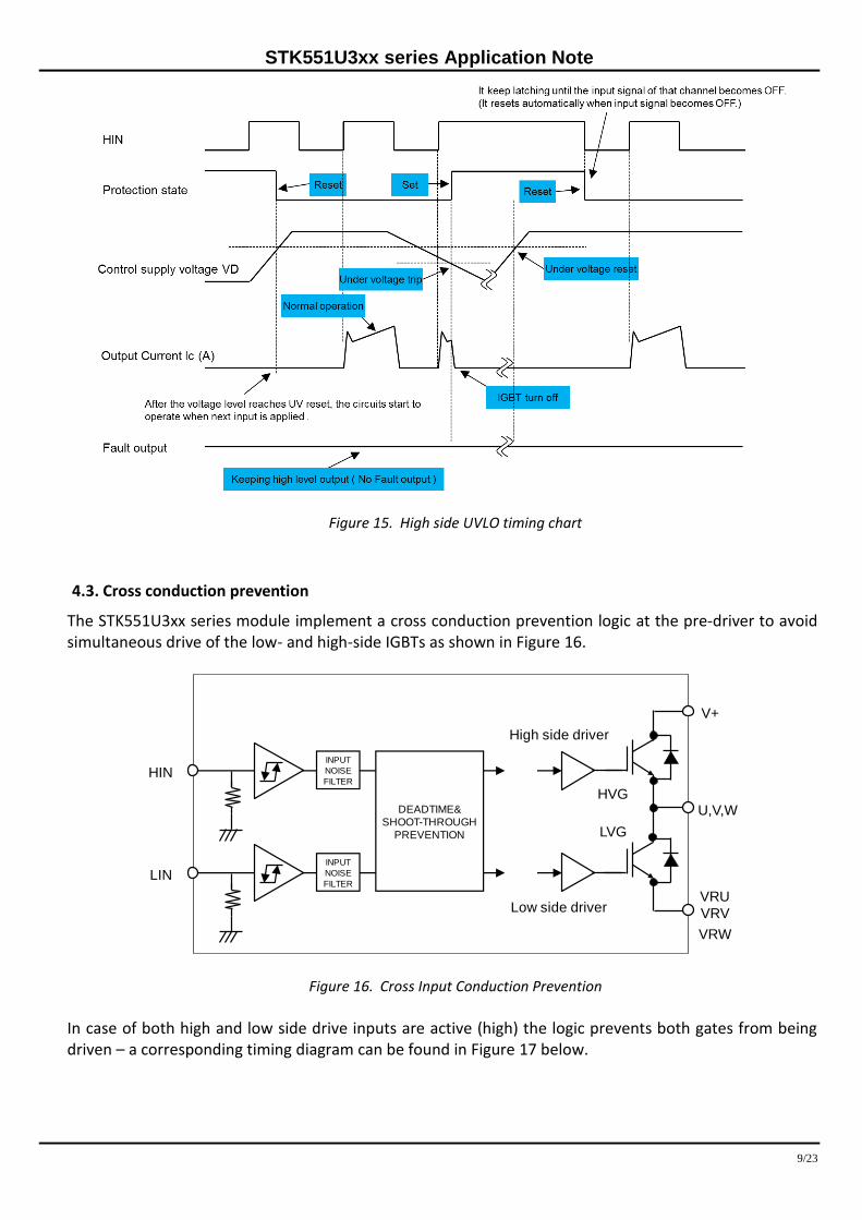
Figure 15. High side UVLO timing chart
4.3. Cross conduction prevention
The STK551U3xx series module implement a cross conduction prevention logic at the pre-driver to avoid simultaneous drive of the low- and high-side IGBTs as shown in Figure 16.
Figure 16. Cross Input Conduction Prevention
In case of both high and low side drive inputs are active (high) the logic prevents both gates from being driven – a corresponding timing diagram can be found in Figure 17 below.
U,V,W
INPUT
NOISE
FILTER
INPUT
NOISE
FILTER
DEADTIME&
SHOOT-THROUGH
PREVENTION
HIN
LIN
V+
VRV
VRU
VRW
High side driver
Low side driver
HVG
LVG
STK551U3xx series Application Note
10/23
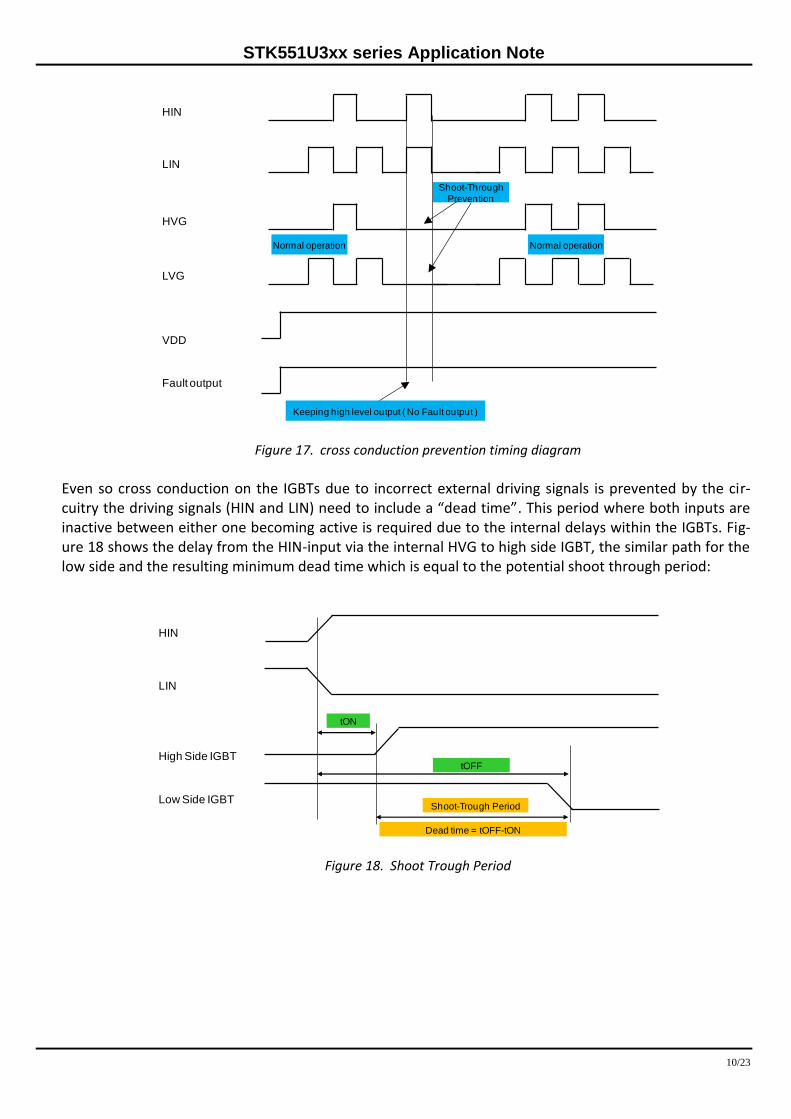
Figure 17. cross conduction prevention timing diagram
Even so cross conduction on the IGBTs due to incorrect external driving signals is prevented by the cir-cuitry the driving signals (HIN and LIN) need to include a “dead time”. This period where both inputs are inactive between either one becoming active is required due to the internal delays within the IGBTs. Fig-ure 18 shows the delay from the HIN-input via the internal HVG to high side IGBT, the similar path for the low side and the resulting minimum dead time which is equal to the potential shoot through period:
Figure 18. Shoot Trough Period
HIN
Fault output
Normal operation
Keeping high level output ( No Fault output )
LIN
HVG
LVG
VDD
Normal operation
Shoot-Through
Prevention
HIN
Low Side IGBT
LIN
High Side IGBTtOFF
Shoot-Trough Period
Dead time = tOFF-tON
tON
STK551U3xx series Application Note
11/23
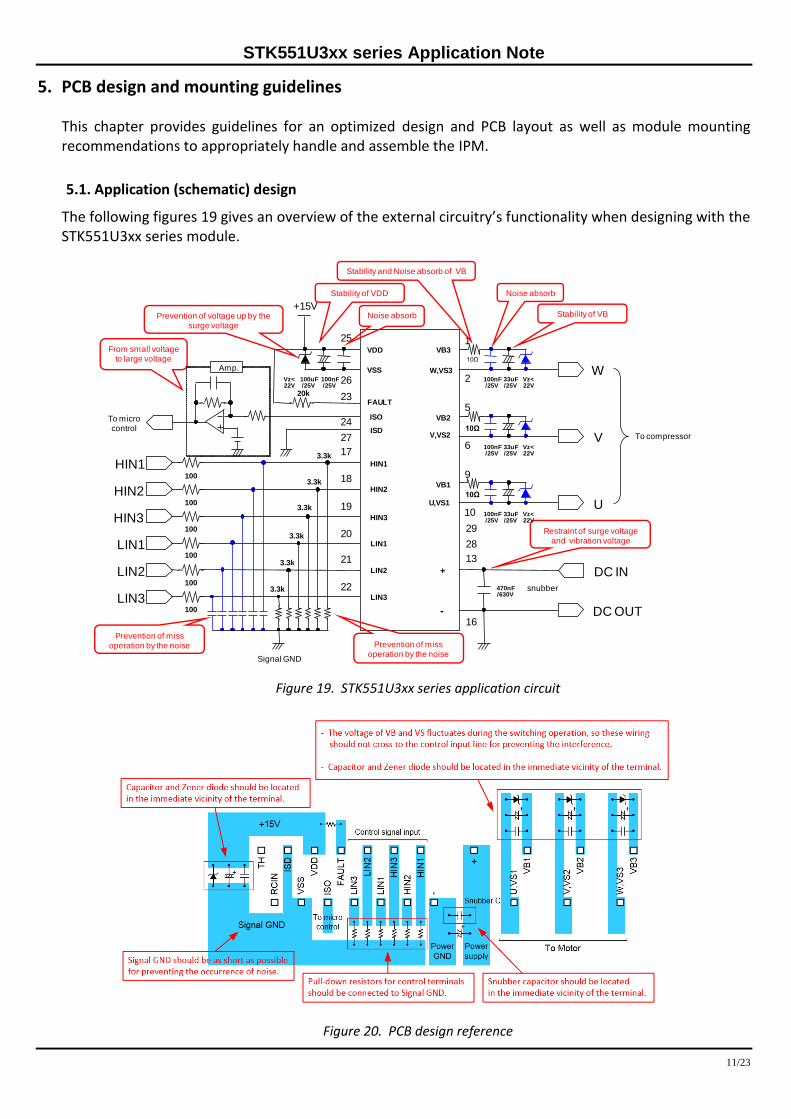
5. PCB design and mounting guidelines
This chapter provides guidelines for an optimized design and PCB layout as well as module mounting recommendations to appropriately handle and assemble the IPM.
5.1. Application (schematic) design
The following figures 19 gives an overview of the external circuitry’s functionality when designing with the STK551U3xx series module.
Figure 19. STK551U3xx series application circuit
Figure 20. PCB design reference
Signal GND
To microcontrol
From small voltage to large voltage
Prevention of voltage up by the surge voltage
Stability of VDD Noise absorb
Stability of VB
To compressor
Restraint of surge voltage and vibration voltage
snubber
Prevention of miss operation by the noise
(9)
(6)
TH
RCIN 28
29
(11)
W
1
2
V
5
6
U
9
10
100nF/25V
33uF/25V
Vz<22V
VB3
W,VS3
100nF/25V
33uF/25V
Vz<22V
100nF/25V
33uF/25V
Vz<22V
VB2
V,VS2
U,VS1
VB1
+
-
DC IN470nF/630V
DC OUT
25
100nF/25V
100uF/25V
Vz<22V
+15V
VDD
VSS
26
20k 23FAULT
HIN1
HIN2
HIN3
LIN1
LIN2
LIN3
100
100
100
100
100
100
3.3k
3.3k
3.3k
3.3k
3.3k
3.3kHIN1
HIN2
HIN3
LIN1
LIN2
LIN3
17
18
19
20
21
22
13
16
ISO
ISD27
24
Amp.
10Ω
10Ω
10Ω
Stability and Noise absorb of VB
Noise absorb
Prevention of miss operation by the noise
STK551U3xx series Application Note
12/23
5.2. Pin by pin design and usage notes
This section provides pin by pin PCB layout recommendations and usage notes. For a complete list of module pins refer to the datasheet or Chapter 6. + & - These pins are connected with the main DC power supply. The applied voltage is up to
the Vcc level. Overvoltage on these pins could be generated by voltage spikes during switching at the floating inductance of the wiring. To avoid this behavior the wire trac-es need to be as short as possible to reduce the floating inductance. In addition a snubber capacitor needs to be placed as close as possible to these pins to stabilize the voltage and absorb voltage surges.
U, V, W These terminals are the output pins for connecting the 3-phase motor. They share the same GND potential with each of the high side control power supplies. Therefore they are also used to connect the GND of the of the bootstrap capacitors. These bootstrap capacitors should be placed as close to the module as possible.
VDD, VSS These pins connect with the circuitry of the internal protection and pre-drivers for the low -side power elements and also with the control power supply of the logic circuitry. Voltage to input these terminals is monitored by the under voltage protection circuit. The VSS terminal is the reference voltage for the control inputs signals as well as Fault and ISO. VSS is connected with the “ - “ terminal internally. The main circuit does typi-cally not draw current from VSS. When the “ - “ and “VSS” pins are connected externally care must be taken to select a single connection point as close as possible to the IC. In case of multiple connections to these pins and longer traces being used, the overcurrent protection level may become low. Therefor this should be avoided.
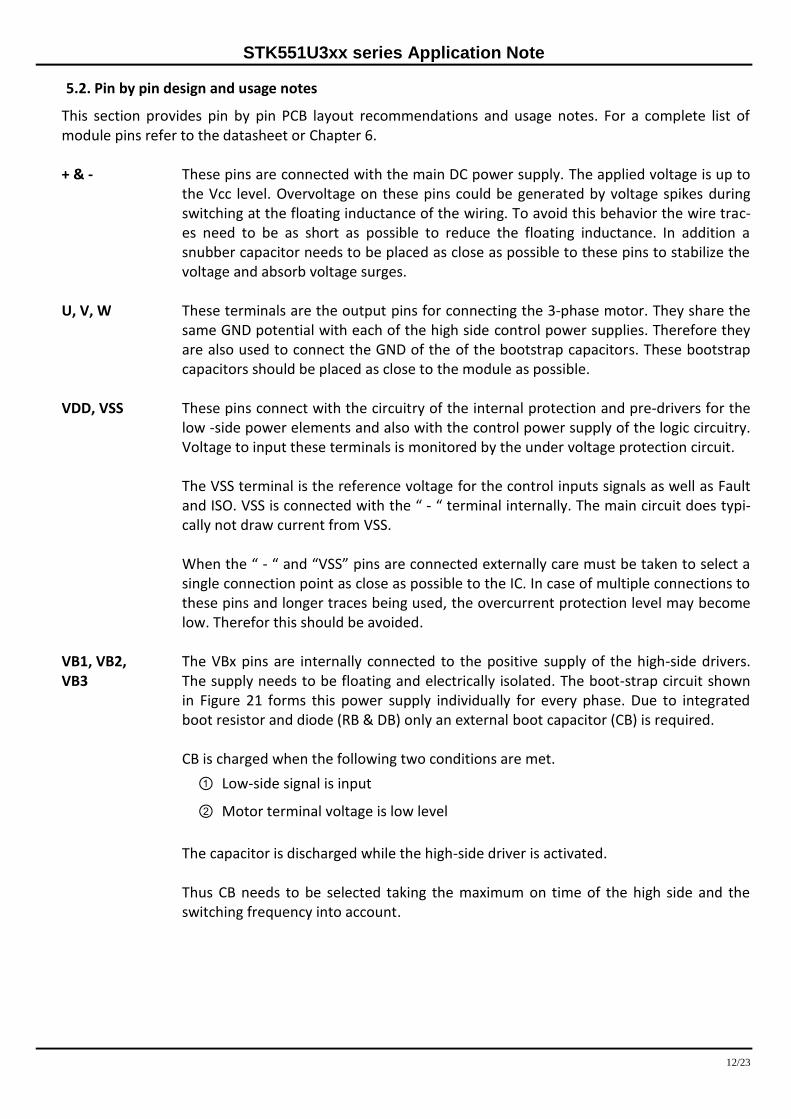
VB1, VB2, VB3
The VBx pins are internally connected to the positive supply of the high-side drivers. The supply needs to be floating and electrically isolated. The boot-strap circuit shown in Figure 21 forms this power supply individually for every phase. Due to integrated boot resistor and diode (RB & DB) only an external boot capacitor (CB) is required. CB is charged when the following two conditions are met.
① Low-side signal is input
② Motor terminal voltage is low level
The capacitor is discharged while the high-side driver is activated. Thus CB needs to be selected taking the maximum on time of the high side and the switching frequency into account.
STK551U3xx series Application Note
13/23
Figure 21. Boot Strap Circuit
The voltages on the high side drivers are individually monitored by the under voltage protection circuit. In case an UVP event is detected on a phase its operation is stopped.
Typically a CB value of less or equal 47uF (±20%) is used. In case the CB value needs to be higher an external resistor (of apx. 20Ω or less) should be used in series with the capacitor to avoid high currents which can cause malfunction of the IPM.
HIN1, LIN1, HIN2, LIN2, HIN3, LIN3
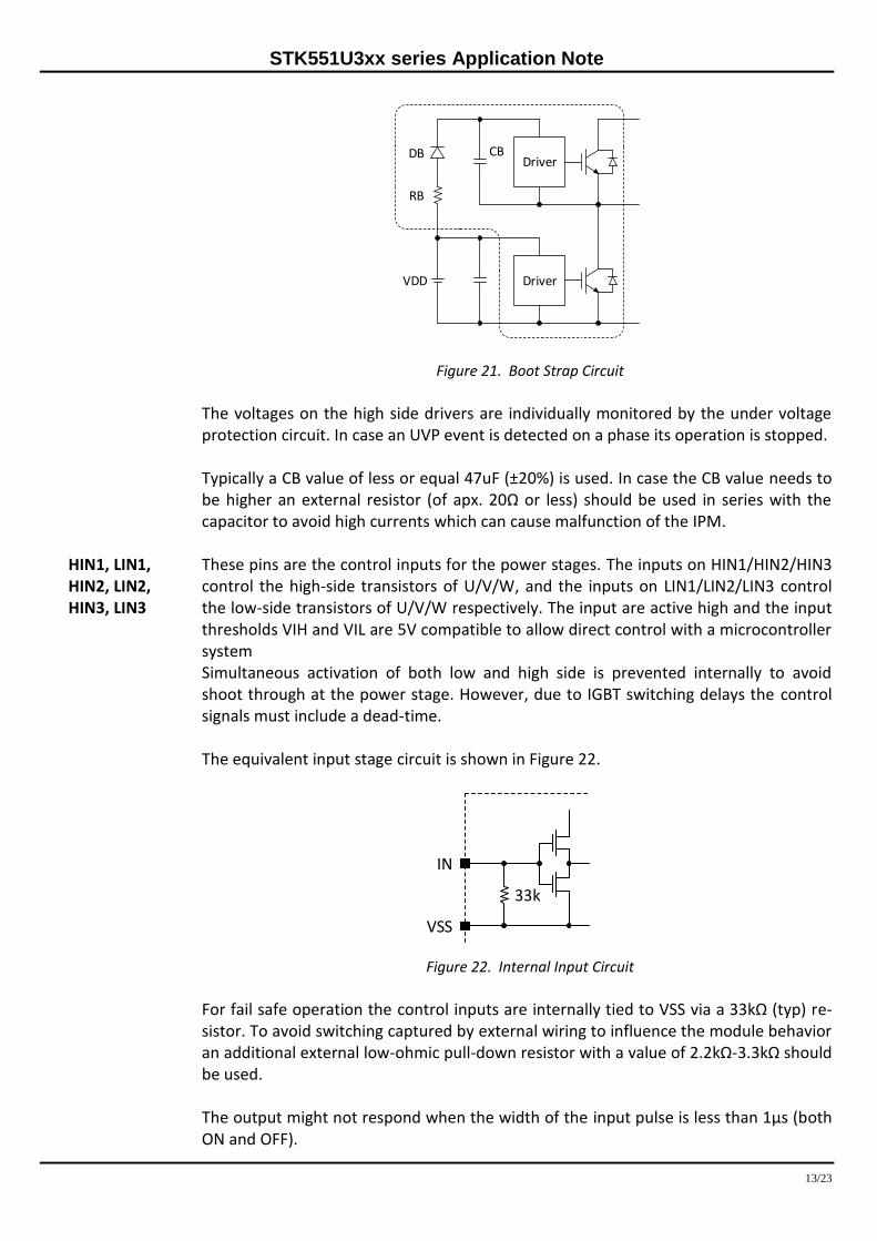
These pins are the control inputs for the power stages. The inputs on HIN1/HIN2/HIN3 control the high-side transistors of U/V/W, and the inputs on LIN1/LIN2/LIN3 control the low-side transistors of U/V/W respectively. The input are active high and the input thresholds VIH and VIL are 5V compatible to allow direct control with a microcontroller system Simultaneous activation of both low and high side is prevented internally to avoid shoot through at the power stage. However, due to IGBT switching delays the control signals must include a dead-time. The equivalent input stage circuit is shown in Figure 22.
Figure 22. Internal Input Circuit
For fail safe operation the control inputs are internally tied to VSS via a 33kΩ (typ) re-sistor. To avoid switching captured by external wiring to influence the module behavior an additional external low-ohmic pull-down resistor with a value of 2.2kΩ-3.3kΩ should be used. The output might not respond when the width of the input pulse is less than 1µs (both ON and OFF).
Driver
DriverCBDB
VDD
RB
IN
VSS
33k
STK551U3xx series Application Note
14/23
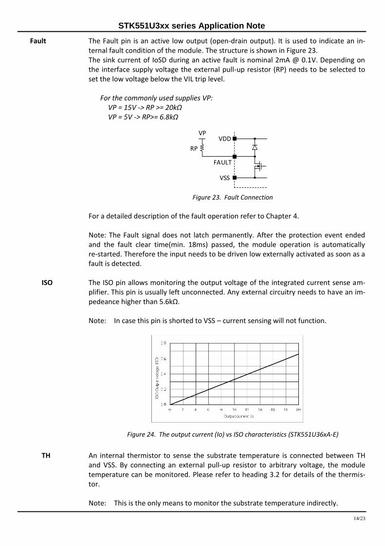
Fault The Fault pin is an active low output (open-drain output). It is used to indicate an in-ternal fault condition of the module. The structure is shown in Figure 23. The sink current of IoSD during an active fault is nominal 2mA @ 0.1V. Depending on the interface supply voltage the external pull-up resistor (RP) needs to be selected to set the low voltage below the VIL trip level. For the commonly used supplies VP: VP = 15V -> RP >= 20kΩ VP = 5V -> RP>= 6.8kΩ
Figure 23. Fault Connection
For a detailed description of the fault operation refer to Chapter 4. Note: The Fault signal does not latch permanently. After the protection event ended and the fault clear time(min. 18ms) passed, the module operation is automatically re-started. Therefore the input needs to be driven low externally activated as soon as a fault is detected.
ISO The ISO pin allows monitoring the output voltage of the integrated current sense am-
plifier. This pin is usually left unconnected. Any external circuitry needs to have an im-pedeance higher than 5.6kΩ. Note: In case this pin is shorted to VSS – current sensing will not function.
Figure 24. The output current (Io) vs ISO characteristics (STK551U36xA-E)
TH An internal thermistor to sense the substrate temperature is connected between TH and VSS. By connecting an external pull-up resistor to arbitrary voltage, the module temperature can be monitored. Please refer to heading 3.2 for details of the thermis-tor. Note: This is the only means to monitor the substrate temperature indirectly.
FAULT
VDD
VSS
VP
RP
STK551U3xx series Application Note
15/23
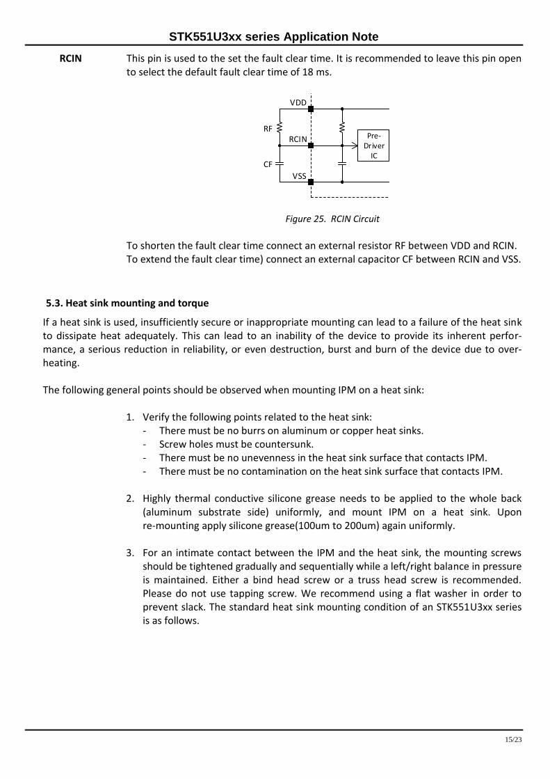
RCIN This pin is used to the set the fault clear time. It is recommended to leave this pin open to select the default fault clear time of 18 ms.
Figure 25. RCIN Circuit
To shorten the fault clear time connect an external resistor RF between VDD and RCIN. To extend the fault clear time) connect an external capacitor CF between RCIN and VSS.
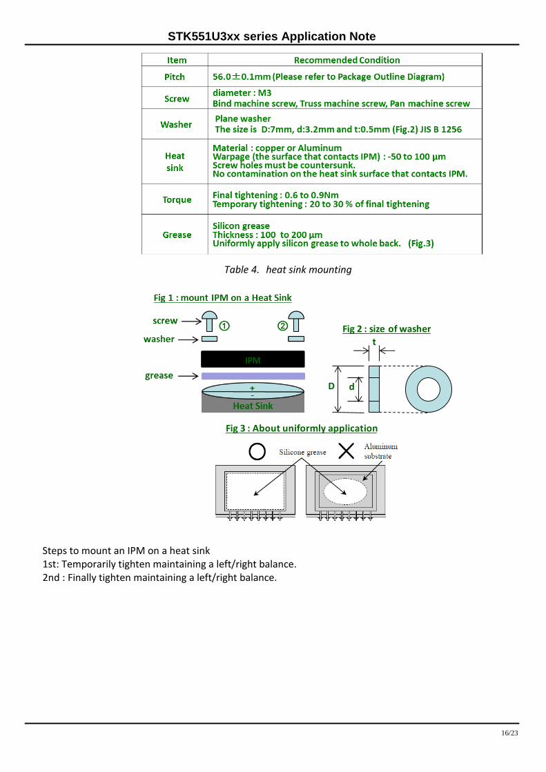
5.3. Heat sink mounting and torque
If a heat sink is used, insufficiently secure or inappropriate mounting can lead to a failure of the heat sink to dissipate heat adequately. This can lead to an inability of the device to provide its inherent perfor-mance, a serious reduction in reliability, or even destruction, burst and burn of the device due to over-heating. The following general points should be observed when mounting IPM on a heat sink:
1. Verify the following points related to the heat sink: - There must be no burrs on aluminum or copper heat sinks. - Screw holes must be countersunk. - There must be no unevenness in the heat sink surface that contacts IPM. - There must be no contamination on the heat sink surface that contacts IPM.
2. Highly thermal conductive silicone grease needs to be applied to the whole back
(aluminum substrate side) uniformly, and mount IPM on a heat sink. Upon re-mounting apply silicone grease(100um to 200um) again uniformly.
3. For an intimate contact between the IPM and the heat sink, the mounting screws should be tightened gradually and sequentially while a left/right balance in pressure is maintained. Either a bind head screw or a truss head screw is recommended. Please do not use tapping screw. We recommend using a flat washer in order to prevent slack. The standard heat sink mounting condition of an STK551U3xx series is as follows.
Pre-Driver
IC
RCIN
VDD
VSS
RF
CF
STK551U3xx series Application Note
16/23
Table 4. heat sink mounting
Steps to mount an IPM on a heat sink 1st: Temporarily tighten maintaining a left/right balance. 2nd : Finally tighten maintaining a left/right balance.
D d
tFig 2 : size of washer
Fig 3 : About uniformly application
STK551U3xx series Application Note
17/23
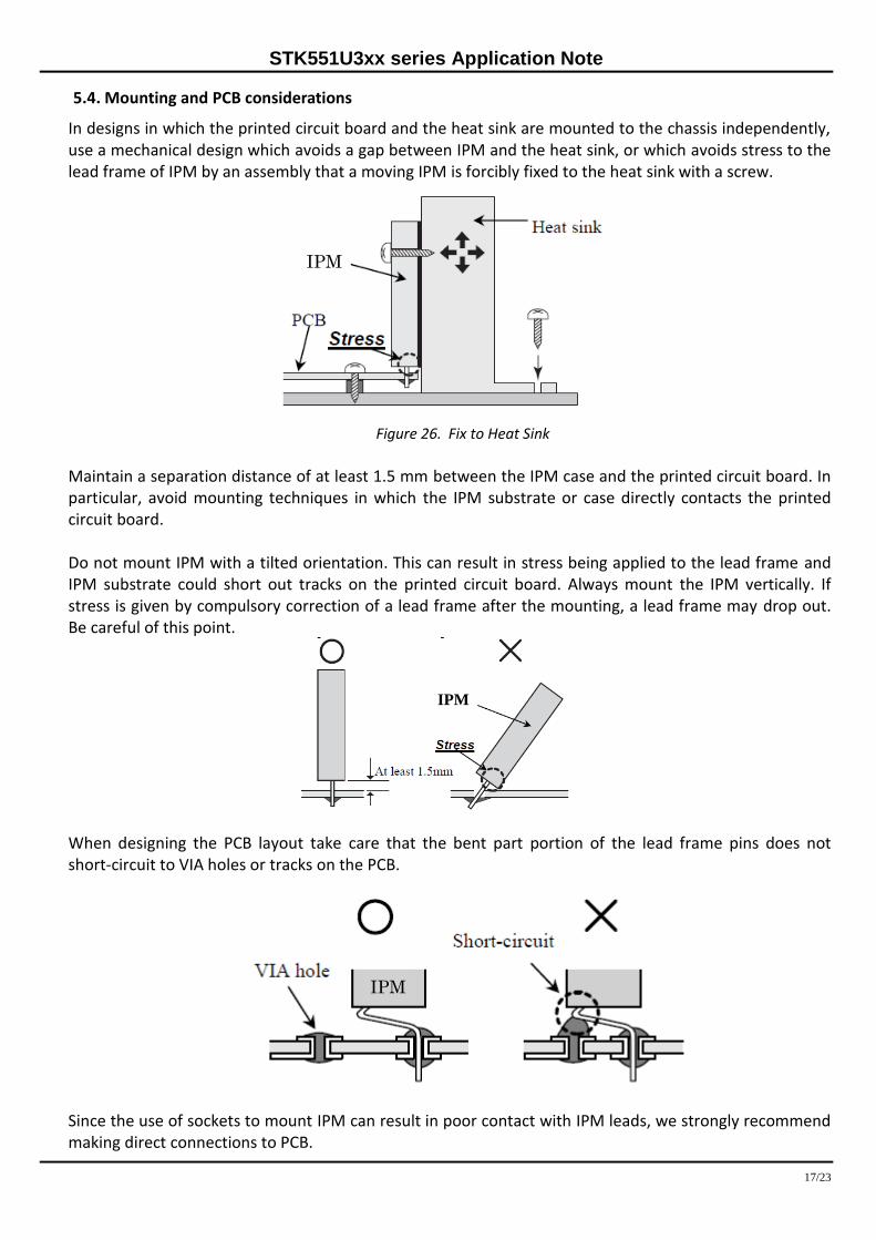
5.4. Mounting and PCB considerations
In designs in which the printed circuit board and the heat sink are mounted to the chassis independently, use a mechanical design which avoids a gap between IPM and the heat sink, or which avoids stress to the lead frame of IPM by an assembly that a moving IPM is forcibly fixed to the heat sink with a screw.
Figure 26. Fix to Heat Sink
Maintain a separation distance of at least 1.5 mm between the IPM case and the printed circuit board. In particular, avoid mounting techniques in which the IPM substrate or case directly contacts the printed circuit board.
Do not mount IPM with a tilted orientation. This can result in stress being applied to the lead frame and IPM substrate could short out tracks on the printed circuit board. Always mount the IPM vertically. If stress is given by compulsory correction of a lead frame after the mounting, a lead frame may drop out. Be careful of this point.
When designing the PCB layout take care that the bent part portion of the lead frame pins does not short-circuit to VIA holes or tracks on the PCB.
Since the use of sockets to mount IPM can result in poor contact with IPM leads, we strongly recommend making direct connections to PCB.
IPM
IPM
IPM
STK551U3xx series Application Note
18/23
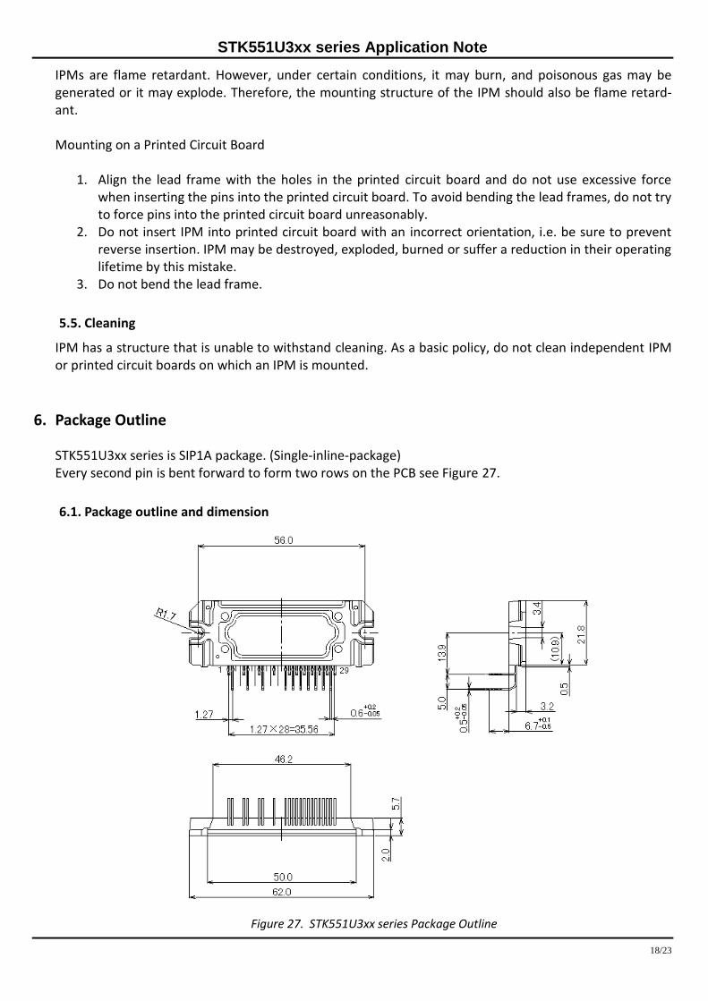
IPMs are flame retardant. However, under certain conditions, it may burn, and poisonous gas may be generated or it may explode. Therefore, the mounting structure of the IPM should also be flame retard-ant.
Mounting on a Printed Circuit Board
1. Align the lead frame with the holes in the printed circuit board and do not use excessive force when inserting the pins into the printed circuit board. To avoid bending the lead frames, do not try to force pins into the printed circuit board unreasonably.
2. Do not insert IPM into printed circuit board with an incorrect orientation, i.e. be sure to prevent reverse insertion. IPM may be destroyed, exploded, burned or suffer a reduction in their operating lifetime by this mistake.
3. Do not bend the lead frame.
5.5. Cleaning
IPM has a structure that is unable to withstand cleaning. As a basic policy, do not clean independent IPM or printed circuit boards on which an IPM is mounted.
6. Package Outline
STK551U3xx series is SIP1A package. (Single-inline-package) Every second pin is bent forward to form two rows on the PCB see Figure 27.
6.1. Package outline and dimension
Figure 27. STK551U3xx series Package Outline
STK551U3xx series Application Note
19/23
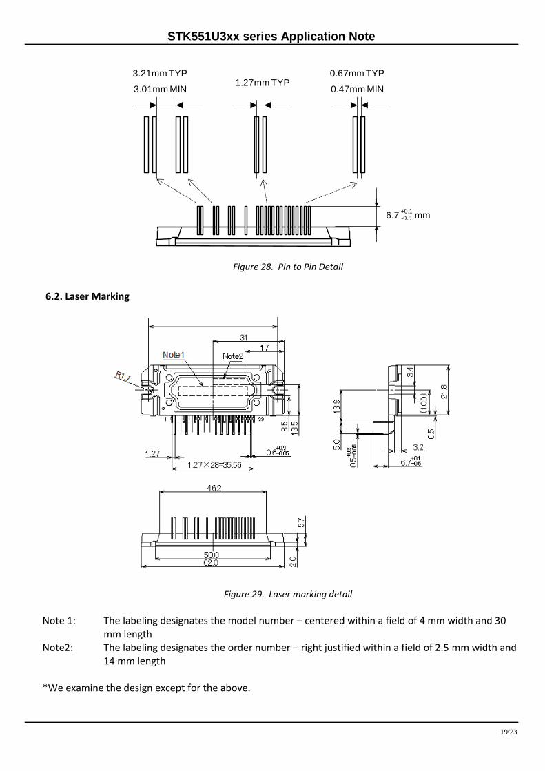
Figure 28. Pin to Pin Detail
6.2. Laser Marking
Figure 29. Laser marking detail
Note 1: The labeling designates the model number – centered within a field of 4 mm width and 30
mm length Note2: The labeling designates the order number – right justified within a field of 2.5 mm width and
14 mm length *We examine the design except for the above.
3.01mm MIN
3.21mm TYP1.27mm TYP
0.47mm MIN
0.67mm TYP
6.7+0.1-0.5 mm
STK551U3xx series Application Note
20/23
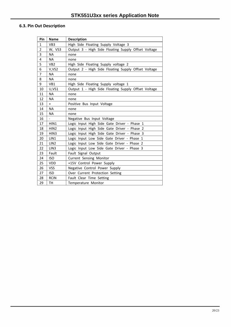
6.3. Pin Out Description
Pin Name Description
1 VB3 High Side Floating Supply Voltage 3
2 W, VS3 Output 3 - High Side Floating Supply Offset Voltage
3 NA none
4 NA none
5 VB2 High Side Floating Supply voltage 2
6 V,VS2 Output 2 - High Side Floating Supply Offset Voltage
7 NA none
8 NA none
9 VB1 High Side Floating Supply voltage 1
10 U,VS1 Output 1 - High Side Floating Supply Offset Voltage
11 NA none
12 NA none
13 + Positive Bus Input Voltage
14 NA none
15 NA none
16 - Negative Bus Input Voltage
17 HIN1 Logic Input High Side Gate Driver - Phase 1
18 HIN2 Logic Input High Side Gate Driver - Phase 2
19 HIN3 Logic Input High Side Gate Driver - Phase 3
20 LIN1 Logic Input Low Side Gate Driver - Phase 1
21 LIN2 Logic Input Low Side Gate Driver - Phase 2
22 LIN3 Logic Input Low Side Gate Driver - Phase 3
23 Fault Fault Signal Output
24 ISO Current Sensing Monitor
25 VDD +15V Control Power Supply
26 VSS Negative Control Power Supply
27 ISD Over Current Protection Setting
28 RCIN Fault Clear Time Setting
29 TH Temperature Monitor
STK551U3xx series Application Note
21/23
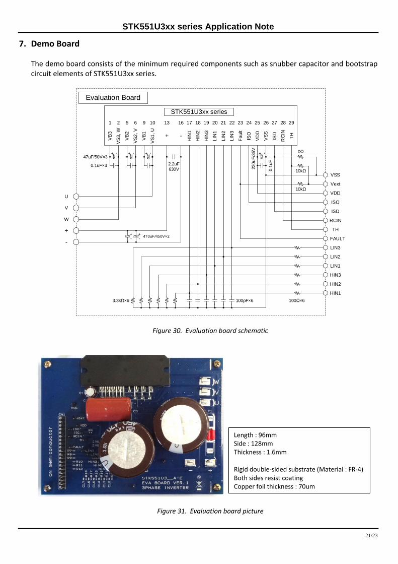
7. Demo Board
The demo board consists of the minimum required components such as snubber capacitor and bootstrap circuit elements of STK551U3xx series.
Figure 30. Evaluation board schematic
Figure 31. Evaluation board picture
Evaluation Board
STK551U3xx series
U
V
W
+
-
VSS
Vext
VDD
ISO
RCIN
ISD
TH
FAULT
LIN3
LIN2
LIN1
HIN3
HIN2
HIN1
1 2 5 6 9 10 16 17 18 19 20 21 22 23 24 25 26 2713 28 29
VB
3
VS
3, W
VB
2
VB
1
-
HIN
1
Fa
ult
ISO
VD
D
VS
S
ISD+
RC
IN
TH
VS
2, V
VS
1,
U
HIN
2
HIN
3
LIN
1
LIN
2
LIN
3
47uF/50V×3
+ - + - + -
0.1uF×3
220
uF
/35V
2.2uF630V
+-
+-
470uF/450V×2
0.1
uF
+ -
3.3kΩ×6 100pF×6 100Ω×6
0Ω
10kΩ
10kΩ
Length : 96mm Side : 128mm Thickness : 1.6mm Rigid double-sided substrate (Material : FR-4) Both sides resist coating Copper foil thickness : 70um
STK551U3xx series Application Note
22/23
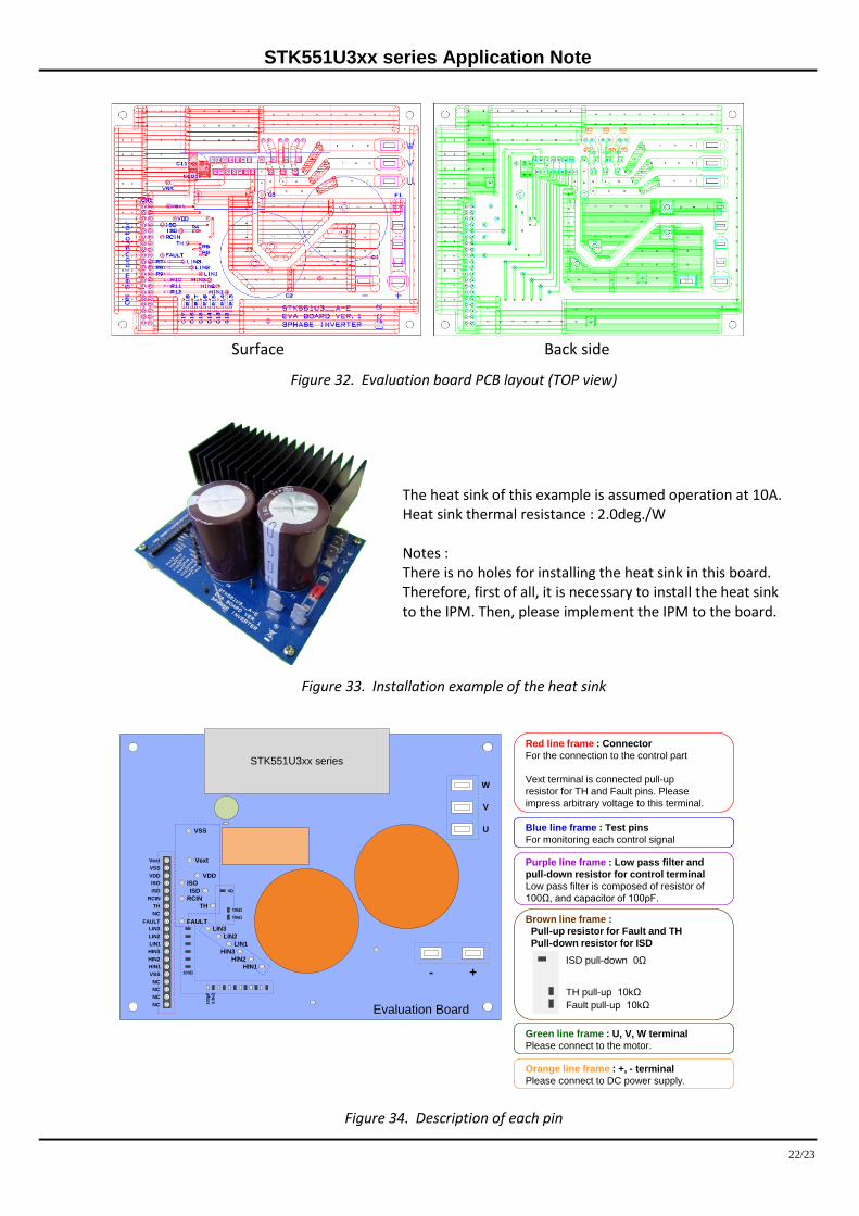
Surface Back side
Figure 32. Evaluation board PCB layout (TOP view)
Figure 33. Installation example of the heat sink
Figure 34. Description of each pin
STK551U3xx series
VSS
Vext
VDD
ISO
ISD
FAULT
TH
LIN3
LIN2
LIN1
HIN3
HIN2
HIN1
W
V
U
- +
RCIN
100Ω
10
0pF
3.3
kΩ
0Ω
10kΩ
10kΩ
VSS
Vext
VDD
ISO
ISD
RCIN
TH
FAULT
LIN3
LIN2
LIN1
HIN3
HIN2
HIN1
NC
NC
VSS
NC
NC
NC
Evaluation Board
Red line frame : Connector
For the connection to the control part
Vext terminal is connected pull-up
resistor for TH and Fault pins. Please
impress arbitrary voltage to this terminal.
ISD pull-down 0Ω
TH pull-up 10kΩ
Fault pull-up 10kΩ
Blue line frame : Test pins
For monitoring each control signal
Purple line frame : Low pass filter and
pull-down resistor for control terminal
Low pass filter is composed of resistor of
100Ω, and capacitor of 100pF.
Brown line frame :
Pull-up resistor for Fault and TH
Pull-down resistor for ISD
Green line frame : U, V, W terminal
Please connect to the motor.
Orange line frame : +, - terminal
Please connect to DC power supply.
The heat sink of this example is assumed operation at 10A. Heat sink thermal resistance : 2.0deg./W Notes : There is no holes for installing the heat sink in this board. Therefore, first of all, it is necessary to install the heat sink to the IPM. Then, please implement the IPM to the board.
STK551U3xx series Application Note
23/23
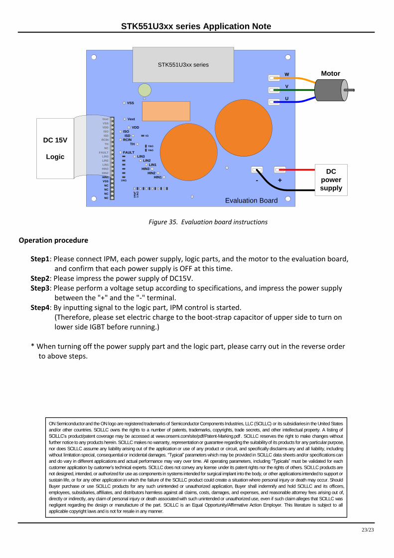
Figure 35. Evaluation board instructions
Operation procedure
Step1: Please connect IPM, each power supply, logic parts, and the motor to the evaluation board, and confirm that each power supply is OFF at this time. Step2: Please impress the power supply of DC15V. Step3: Please perform a voltage setup according to specifications, and impress the power supply between the "+" and the "-" terminal. Step4: By inputting signal to the logic part, IPM control is started. (Therefore, please set electric charge to the boot-strap capacitor of upper side to turn on lower side IGBT before running.)
* When turning off the power supply part and the logic part, please carry out in the reverse order to above steps.
DC 15V
Logic
STK551U3xx series
VSS
Vext
VDD
ISO
ISD
FAULT
TH
LIN3
LIN2
LIN1
HIN3
HIN2
HIN1
W
V
U
- +
RCIN
100Ω
10
0pF
3.3
kΩ
0Ω
10kΩ
10kΩ
VSS
Vext
VDD
ISO
ISD
RCIN
TH
FAULT
LIN3
LIN2
LIN1
HIN3
HIN2
HIN1
NC
NC
VSS
NC
NC
NC
Evaluation Board
Motor
DC
power
supply
ON Semiconductorand the ON logo are registered trademarks of SemiconductorComponents Industries, LLC (SCILLC) or its subsidiariesin the United States
and/or other countries. SCILLC owns the rights to a number of patents, trademarks, copyrights, trade secrets, and other intellectual property. A listing of
SCILLC’s product/patent coverage may be accessed at www.onsemi.com/site/pdf/Patent-Marking.pdf . SCILLC reserves the right to make changes without
further notice to any products herein. SCILLC makes no warranty, representationor guarantee regarding the suitabilityof its products for any particular purpose,
nor does SCILLC assume any liability arising out of the application or use of any product or circuit, and specifically disclaims any and all liability, including
without limitation special, consequential or incidental damages. “Typical” parameters which may be provided in SCILLC data sheets and/or specificationscan
and do vary in different applications and actual performance may vary over time. All operating parameters, including “Typicals” must be validated for each
customer application by customer’s technical experts. SCILLC does not convey any license under its patent rights nor the rights of others. SCILLC products are
not designed, intended, or authorized for use as components in systems intended for surgical implant into the body, or other applicationsintended to support or
sustain life, or for any other application in which the failure of the SCILLC product could create a situation where personal injury or death may occur. Should
Buyer purchase or use SCILLC products for any such unintended or unauthorized application, Buyer shall indemnify and hold SCILLC and its officers,
employees, subsidiaries, affiliates, and distributors harmless against all claims, costs, damages, and expenses, and reasonable attorney fees arising out of,
directly or indirectly, any claim of personal injury or death associatedwith such unintended or unauthorized use, even if such claim alleges that SCILLC was
negligent regarding the design or manufacture of the part. SCILLC is an Equal Opportunity/Affirmative Action Employer. This literature is subject to all
applicable copyright laws and is not for resale in any manner.