Embed Size (px)
Citation preview
May 2019 ES0445 Rev 1 1/23
1
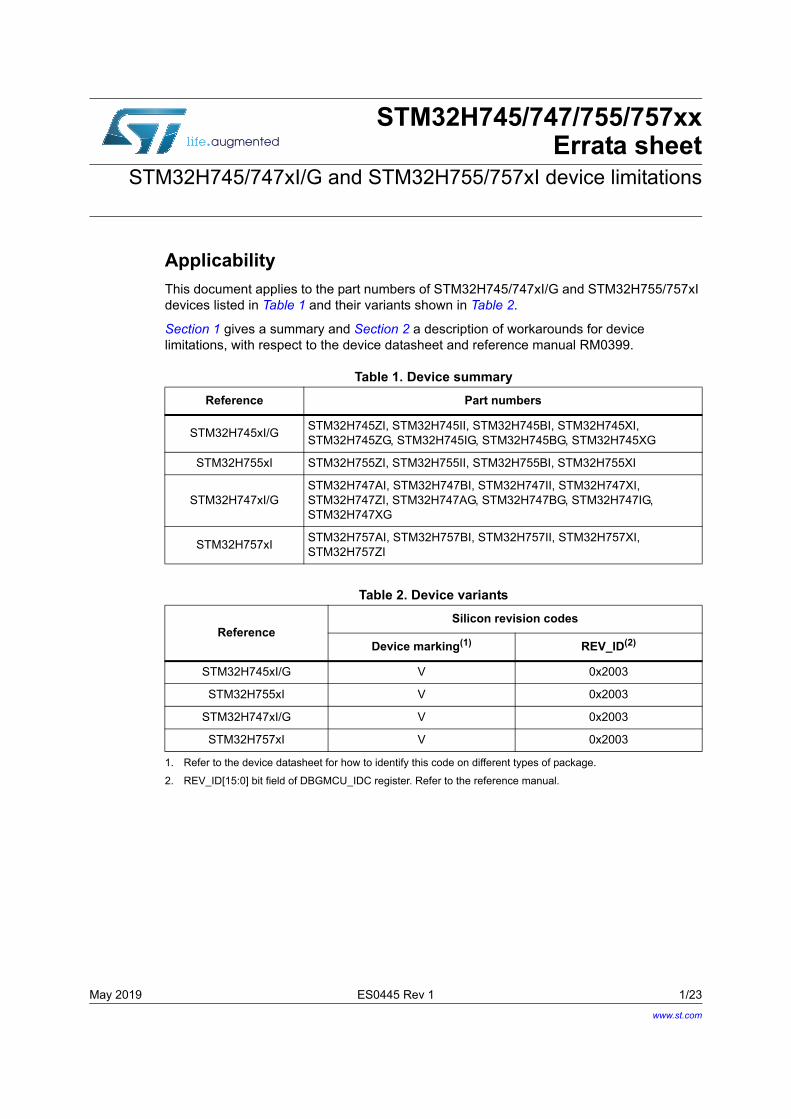
STM32H745/747/755/757xxErrata sheet
STM32H745/747xI/G and STM32H755/757xI device limitations
Applicability
This document applies to the part numbers of STM32H745/747xI/G and STM32H755/757xI devices listed in Table 1 and their variants shown in Table 2.
Section 1 gives a summary and Section 2 a description of workarounds for device limitations, with respect to the device datasheet and reference manual RM0399.
Table 1. Device summary
Reference Part numbers
STM32H745xI/GSTM32H745ZI, STM32H745II, STM32H745BI, STM32H745XI, STM32H745ZG, STM32H745IG, STM32H745BG, STM32H745XG
STM32H755xI STM32H755ZI, STM32H755II, STM32H755BI, STM32H755XI
STM32H747xI/GSTM32H747AI, STM32H747BI, STM32H747II, STM32H747XI, STM32H747ZI, STM32H747AG, STM32H747BG, STM32H747IG, STM32H747XG
STM32H757xISTM32H757AI, STM32H757BI, STM32H757II, STM32H757XI, STM32H757ZI
Table 2. Device variants
ReferenceSilicon revision codes
Device marking(1)
1. Refer to the device datasheet for how to identify this code on different types of package.
REV_ID(2)
2. REV_ID[15:0] bit field of DBGMCU_IDC register. Refer to the reference manual.
STM32H745xI/G V 0x2003
STM32H755xI V 0x2003
STM32H747xI/G V 0x2003
STM32H757xI V 0x2003
www.st.com
Contents STM32H745/747/755/757xx
2/23 ES0445 Rev 1
Contents
1 Summary of device limitations . . . . . . . . . . . . . . . . . . . . . . . . . . . . . . . . 4
2 Description of device limitations . . . . . . . . . . . . . . . . . . . . . . . . . . . . . . . 6
2.1 Arm® 32-bit Cortex®-M4 core . . . . . . . . . . . . . . . . . . . . . . . . . . . . . . . . . . 6
2.1.1 Interrupted loads to SP can cause erroneous behavior . . . . . . . . . . . . . . 6
2.1.2 VDIV or VSQRT instructions might not complete correctly when very short ISRs are used . . . . . . . . . . . . . . . . . . . . . . . . . . . . . . . . . . . . . . . . . 7
2.2 Arm® 32-bit Cortex®-M7 core . . . . . . . . . . . . . . . . . . . . . . . . . . . . . . . . . . 8
2.2.1 Cortex®-M7 data corruption when using Data cache configured in write-through . . . . . . . . . . . . . . . . . . . . . . . . . . . . . . . . . . . . . . . . . . . . . . 8
2.2.2 Cortex®-M7 FPU interrupt not present on NVIC line 81 . . . . . . . . . . . . . 9
2.3 System . . . . . . . . . . . . . . . . . . . . . . . . . . . . . . . . . . . . . . . . . . . . . . . . . . . . 9
2.3.1 Device stalled when two consecutive level regressions occur without accessing from/to backup SRAM . . . . . . . . . . . . . . . . . . . . . . . . 9
2.3.2 AXI domain locked when watchdog reset limited to CPU1 or CPU2 . . . . 9
2.3.3 GPIO assigned to DAC cannot be used in output mode when the DAC output is connected to on-chip peripheral . . . . . . . . . . . . . . . . 10
2.3.4 Unstable LSI when it clocks RTC or CSS on LSE . . . . . . . . . . . . . . . . . 10
2.4 FMC . . . . . . . . . . . . . . . . . . . . . . . . . . . . . . . . . . . . . . . . . . . . . . . . . . . . . 10
2.4.1 Dummy read cycles inserted when reading synchronous memories . . . 10
2.4.2 Wrong data read from a busy NAND Flash memory . . . . . . . . . . . . . . . 11
2.5 QUADSPI . . . . . . . . . . . . . . . . . . . . . . . . . . . . . . . . . . . . . . . . . . . . . . . . . .11
2.5.1 QUADSPI_CCR hangs when QUADSPI_CR is cleared . . . . . . . . . . . . 11
2.5.2 QUADSPI cannot be used in Indirect read mode when only data phase is activated . . . . . . . . . . . . . . . . . . . . . . . . . . . . . . . . . . . . . 11
2.6 LCD-TFT . . . . . . . . . . . . . . . . . . . . . . . . . . . . . . . . . . . . . . . . . . . . . . . . . 12
2.6.1 Device stalled when accessing LTDC registers while pixel clock is disabled . . . . . . . . . . . . . . . . . . . . . . . . . . . . . . . . . . . . . . . . . . . . . . . 12
2.7 DSI . . . . . . . . . . . . . . . . . . . . . . . . . . . . . . . . . . . . . . . . . . . . . . . . . . . . . . 12
2.7.1 Data corruption when accessing DSI Host registers while pixel clock is disabled . . . . . . . . . . . . . . . . . . . . . . . . . . . . . . . . . . . . . . . . . . . . . . . 12
2.8 I2C . . . . . . . . . . . . . . . . . . . . . . . . . . . . . . . . . . . . . . . . . . . . . . . . . . . . . . 12
2.8.1 10-bit master mode: new transfer cannot be launched if first part of the address is not acknowledged by the slave . . . . . . . . . . . . . . . . . 12
2.8.2 Wrong behavior in Stop mode when wakeup from Stop mode is disabled in I2C . . . . . . . . . . . . . . . . . . . . . . . . . . . . . . . . . . . . . 13
ES0445 Rev 1 3/23
STM32H745/747/755/757xx Contents
3
2.8.3 Spurious bus error detection in Master mode . . . . . . . . . . . . . . . . . . . . 13
2.8.4 Spurious master transfer upon own slave address match . . . . . . . . . . . 14
2.8.5 START bit is cleared upon setting ADDRCF, not upon address match . 15
2.9 USART . . . . . . . . . . . . . . . . . . . . . . . . . . . . . . . . . . . . . . . . . . . . . . . . . . . 15
2.9.1 Underrun flag is set when the USART is used in SPI Slave receive mode . . . . . . . . . . . . . . . . . . . . . . . . . . . . . . . . . . . . . . . . . . . . . 15
2.10 SPI . . . . . . . . . . . . . . . . . . . . . . . . . . . . . . . . . . . . . . . . . . . . . . . . . . . . . . 15
2.10.1 Master data transfer stall at system clock much faster than SCK . . . . . 15
2.10.2 Corrupted CRC return at non-zero UDRDET setting . . . . . . . . . . . . . . . 16
2.10.3 TXP interrupt occurring while disabled . . . . . . . . . . . . . . . . . . . . . . . . . 16
2.11 FDCAN . . . . . . . . . . . . . . . . . . . . . . . . . . . . . . . . . . . . . . . . . . . . . . . . . . . 16
2.11.1 Writing FDCAN_TTTS during initialization corrupts FDCAN_TTTMC . . 16
2.11.2 Mis-synchronization in Edge filtering mode when the falling edge at FDCAN_Rx input pin coincides with the end of the integration phase . . . . . . . . . . . . . . . . . . . . . . . . . . . . . . . . . . . . . . . . . . 17
2.11.3 Tx FIFO messages inverted when both Tx buffer and FIFO are used and the messages in the Tx buffer have higher priority than in the Tx FIFO . . . . . . . . . . . . . . . . . . . . . . . . . . . . . . . . . . . . . . . . . . . . 17
2.12 ETH . . . . . . . . . . . . . . . . . . . . . . . . . . . . . . . . . . . . . . . . . . . . . . . . . . . . . 18
2.12.1 Incorrect L4 inverse filtering results for corrupted packets . . . . . . . . . . 18
2.12.2 Rx DMA may fail to recover upon DMA restart following a bus error, with Rx timestamping enabled . . . . . . . . . . . . . . . . . . . . . . . . . . . . . . . . 18
2.12.3 Tx DMA may halt while fetching TSO header under specific conditions 19
2.12.4 Spurious receive watchdog timeout interrupt . . . . . . . . . . . . . . . . . . . . . 19
2.12.5 Incorrect flexible PPS output interval under specific conditions . . . . . . 19
2.12.6 Packets dropped in RMII 10Mbps mode due to fake dribble and CRC error . . . . . . . . . . . . . . . . . . . . . . . . . . . . . . . . . . . . . . . . . . . . 20
2.12.7 ARP offload function not effective . . . . . . . . . . . . . . . . . . . . . . . . . . . . . 20
2.13 HDMI-CEC . . . . . . . . . . . . . . . . . . . . . . . . . . . . . . . . . . . . . . . . . . . . . . . . 21
2.13.1 Unexpected switch to Receive mode without automatic transmission retry and notification . . . . . . . . . . . . . . . . . . . . . . . . . . . . . . . . . . . . . . . 21
2.13.2 CEC header not received due to unjustified Rx-Overrun detection . . . . 21
3 Revision history . . . . . . . . . . . . . . . . . . . . . . . . . . . . . . . . . . . . . . . . . . . 22
Summary of device limitations STM32H745/747/755/757xx
4/23 ES0445 Rev 1
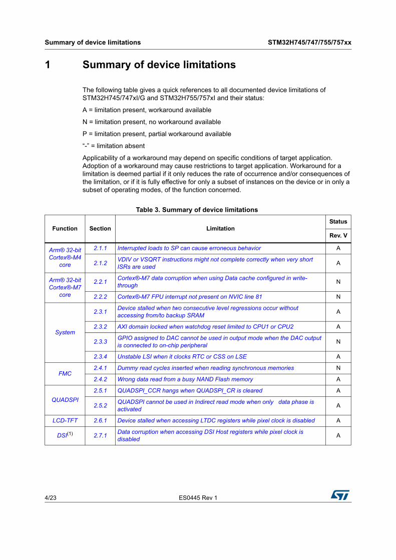
1 Summary of device limitations
The following table gives a quick references to all documented device limitations of STM32H745/747xI/G and STM32H755/757xI and their status:
A = limitation present, workaround available
N = limitation present, no workaround available
P = limitation present, partial workaround available
“-” = limitation absent
Applicability of a workaround may depend on specific conditions of target application. Adoption of a workaround may cause restrictions to target application. Workaround for a limitation is deemed partial if it only reduces the rate of occurrence and/or consequences of the limitation, or if it is fully effective for only a subset of instances on the device or in only a subset of operating modes, of the function concerned.
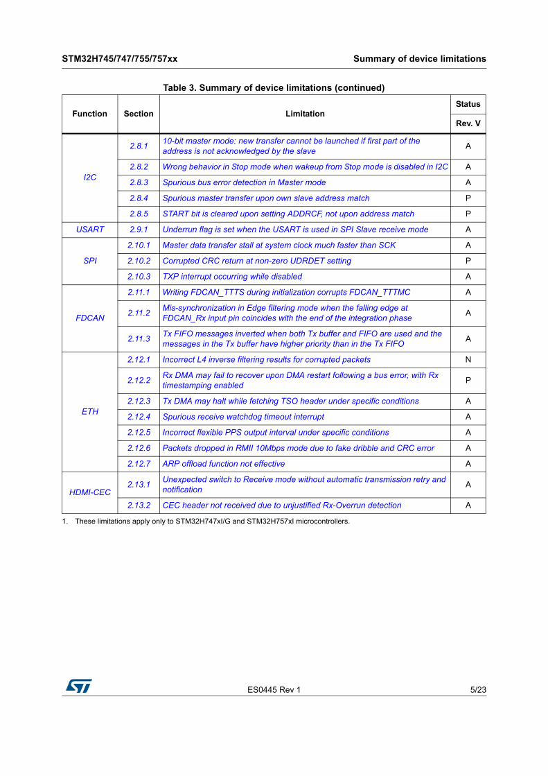
Table 3. Summary of device limitations
Function Section LimitationStatus
Rev. V
Arm® 32-bit Cortex®-M4
core
2.1.1 Interrupted loads to SP can cause erroneous behavior A
2.1.2VDIV or VSQRT instructions might not complete correctly when very short ISRs are used
A
Arm® 32-bit Cortex®-M7
core
2.2.1Cortex®-M7 data corruption when using Data cache configured in write-through
N
2.2.2 Cortex®-M7 FPU interrupt not present on NVIC line 81 N
System
2.3.1Device stalled when two consecutive level regressions occur without accessing from/to backup SRAM
A
2.3.2 AXI domain locked when watchdog reset limited to CPU1 or CPU2 A
2.3.3GPIO assigned to DAC cannot be used in output mode when the DAC output is connected to on-chip peripheral
N
2.3.4 Unstable LSI when it clocks RTC or CSS on LSE A
FMC2.4.1 Dummy read cycles inserted when reading synchronous memories N
2.4.2 Wrong data read from a busy NAND Flash memory A
QUADSPI
2.5.1 QUADSPI_CCR hangs when QUADSPI_CR is cleared A
2.5.2QUADSPI cannot be used in Indirect read mode when only data phase is activated
A
LCD-TFT 2.6.1 Device stalled when accessing LTDC registers while pixel clock is disabled A
DSI(1) 2.7.1Data corruption when accessing DSI Host registers while pixel clock is disabled
A
ES0445 Rev 1 5/23
STM32H745/747/755/757xx Summary of device limitations
5
I2C
2.8.110-bit master mode: new transfer cannot be launched if first part of the address is not acknowledged by the slave
A
2.8.2 Wrong behavior in Stop mode when wakeup from Stop mode is disabled in I2C A
2.8.3 Spurious bus error detection in Master mode A
2.8.4 Spurious master transfer upon own slave address match P
2.8.5 START bit is cleared upon setting ADDRCF, not upon address match P
USART 2.9.1 Underrun flag is set when the USART is used in SPI Slave receive mode A
SPI
2.10.1 Master data transfer stall at system clock much faster than SCK A
2.10.2 Corrupted CRC return at non-zero UDRDET setting P
2.10.3 TXP interrupt occurring while disabled A
FDCAN
2.11.1 Writing FDCAN_TTTS during initialization corrupts FDCAN_TTTMC A
2.11.2Mis-synchronization in Edge filtering mode when the falling edge at FDCAN_Rx input pin coincides with the end of the integration phase
A
2.11.3Tx FIFO messages inverted when both Tx buffer and FIFO are used and the messages in the Tx buffer have higher priority than in the Tx FIFO
A
ETH
2.12.1 Incorrect L4 inverse filtering results for corrupted packets N
2.12.2Rx DMA may fail to recover upon DMA restart following a bus error, with Rx timestamping enabled
P
2.12.3 Tx DMA may halt while fetching TSO header under specific conditions A
2.12.4 Spurious receive watchdog timeout interrupt A
2.12.5 Incorrect flexible PPS output interval under specific conditions A
2.12.6 Packets dropped in RMII 10Mbps mode due to fake dribble and CRC error A
2.12.7 ARP offload function not effective A
HDMI-CEC2.13.1
Unexpected switch to Receive mode without automatic transmission retry and notification
A
2.13.2 CEC header not received due to unjustified Rx-Overrun detection A
1. These limitations apply only to STM32H747xI/G and STM32H757xI microcontrollers.
Table 3. Summary of device limitations (continued)
Function Section LimitationStatus
Rev. V
Description of device limitations STM32H745/747/755/757xx
6/23 ES0445 Rev 1
2 Description of device limitations
The following sections describe device limitations of the applicable Arm(a) core devices and provide workarounds if available. They are grouped by device functions.
2.1 Arm® 32-bit Cortex®-M4 core
Errata notice for the Arm® Cortex®-M4F core revisions r0 is available from http://infocenter.arm.com. Only applicable information from the Arm errata notice is replicated in this document. Extra information may be added for more clarity.
2.1.1 Interrupted loads to SP can cause erroneous behavior
This limitation is registered under Arm ID number 752770 and classified into “Category B”. Its impact to the device is minor.
Description
If an interrupt occurs during the data-phase of a single word load to the stack-pointer (SP/R13), erroneous behavior can occur. In all cases, returning from the interrupt will result in the load instruction being executed an additional time. For all instructions performing an update to the base register, the base register will be erroneously updated on each execution, resulting in the stack-pointer being loaded from an incorrect memory location.
The affected instructions that can result in the load transaction being repeated are:
• LDR SP, [Rn],#imm
• LDR SP, [Rn,#imm]!
• LDR SP, [Rn,#imm]
• LDR SP, [Rn]
• LDR SP, [Rn,Rm]
The affected instructions that can result in the stack-pointer being loaded from an incorrect memory address are:
• LDR SP,[Rn],#imm
• LDR SP,[Rn,#imm]!
As compilers do not generate these particular instructions, the limitation is only likely to occur with hand-written assembly code.
Workaround
Both issues may be worked around by replacing the direct load to the stack-pointer, with an intermediate load to a general-purpose register followed by a move to the stack-pointer.
a. Arm is a registered trademark of Arm Limited (or its subsidiaries) in the US and/or elsewhere.
ES0445 Rev 1 7/23
STM32H745/747/755/757xx Description of device limitations
21
Example:
Replace LDR SP,[R0] with:
LDR R2,[R0]
MOV SP,R2
2.1.2 VDIV or VSQRT instructions might not complete correctly when very short ISRs are used
This limitation is registered under Arm ID number 776924 and classified into “Category B”. Its impact to the device is limited.
Description
The VDIV and VSQRT instructions take 14 cycles to execute. When an interrupt is taken a VDIV or VSQRT instruction is not terminated, and completes its execution while the interrupt stacking occurs. If lazy context save of floating point state is enabled then the automatic stacking of the floating point context does not occur until a floating point instruction is executed inside the interrupt service routine.
Lazy context save is enabled by default. When it is enabled, the minimum time for the first instruction in the interrupt service routine to start executing is 12 cycles. In certain timing conditions, and if there is only one or two instructions inside the interrupt service routine, then the VDIV or VSQRT instruction might not write its result to the register bank or to the FPSCR.
The failure occurs when the following condition is met:
1. The floating point unit is enabled
2. Lazy context saving is not disabled
3. A VDIV or VSQRT is executed
4. The destination register for the VDIV or VSQRT is one of s0 - s15
5. An interrupt occurs and is taken
6. The interrupt service routine being executed does not contain a floating point instruction
7. Within 14 cycles after the VDIV or VSQRT is executed, an interrupt return is executed
A minimum of 12 of these 14 cycles are utilized for the context state stacking, which leaves 2 cycles for instructions inside the interrupt service routine, or 2 wait states applied to the entire stacking sequence (which means that it is not a constant wait state for every access).
In general, this means that if the memory system inserts wait states for stack transactions (that is, external memory is used for stack data), then this erratum cannot be observed.
The effect of this erratum is that the VDIV or VQSRT instruction does not complete correctly and the register bank and FPSCR are not updated, which means that these registers hold incorrect, out of date, data.
Workaround
A workaround is only required if the floating point unit is enabled. A workaround is not required if the stack is in external memory.
Description of device limitations STM32H745/747/755/757xx
8/23 ES0445 Rev 1
There are two possible workarounds:
• Disable lazy context save of floating point state by clearing LSPEN to 0 (bit 30 of the FPCCR at address 0xE000EF34).
• Ensure that every interrupt service routine contains more than 2 instructions in addition to the exception return instruction.
2.2 Arm® 32-bit Cortex®-M7 core
Errata notice for the Arm® processor Cortex®-M7 core revision r0p1 is available from http://infocenter.arm.com.
2.2.1 Cortex®-M7 data corruption when using Data cache configured in write-through
Description
This limitation is registered under Arm® ID number 1259864 and classified into “Category A”.
If a particular sequence of stores and loads is performed to write-through memory, and some timing-based internal conditions are met, then a load might not get the last data stored to that address.
This erratum can only occur if the loads and stores are to write-through memory. This could be due to any of the following:
• The MPU has been programmed to set this address as write-through.
• The default memory map is being used and this address is write-through in that map.
• The memory is cacheable, and the CM7_CACR.FORCEWT bit is set.
• The memory is cacheable, shared, and the CM7_CACR.SIWT bit is set.
The following sequence is required for this erratum to occur:
1. The address of interest must be in the cache.
2. A write-through store to the same doubleword as the address of interest.
3. One of the following:
– A linefill is started (to a different cacheline to the address of interest) that allocates to the same set as the address of interest.
– An ECC error.
– A cache maintenance operation without a following DSB.
4. A store to the address of interest.
5. A load from the address of interest.
If certain specific timing conditions are met, the load will get the data from the first store, or from what was in the cache at the start of the sequence instead of the data from the second store.
The effect of this erratum is that load operations can return incorrect data.
ES0445 Rev 1 9/23
STM32H745/747/755/757xx Description of device limitations
21
Workaround
There is no direct workaround for this erratum.
Where possible, Arm® recommends that you use the MPU to change the attributes on any write-through memory to write-back memory. If this is not possible, it might be necessary to disable the cache for sections of code that access write-through memory.
2.2.2 Cortex®-M7 FPU interrupt not present on NVIC line 81
Description
Arm® Cortex®-M7 FPU interrupt is not mapped on NVIC line 81.
Note: This limitation is due to an error of implementation of the Arm core on the die, as opposed to a limitation of the core itself.
Workaround
None.
2.3 System
2.3.1 Device stalled when two consecutive level regressions occur without accessing from/to backup SRAM
Description
The device might stall when two consecutive level regressions (switching from RDP level 1 to RDP level 0) are performed without accessing (reading/writing) from/to backup SRAM.
A power-on reset is required to recover from this failure.
Workaround
Perform a dummy access to backup SRAM before executing the level regression sequence (switching from RDP level 1 to RDP level 0).
2.3.2 AXI domain locked when watchdog reset limited to CPU1 or CPU2
Description
The AXI domain might get locked when the watchdog reset is limited to CPU1 or CPU2 (WW1RSC or WW2RSC cleared in RCC_GCR register) and a watchdog reset is generated.
Workaround
Configured the watchdog reset scope to reset the full system (WW1RSC or WW2RSC set in RCC_GCR register).
Description of device limitations STM32H745/747/755/757xx
10/23 ES0445 Rev 1
2.3.3 GPIO assigned to DAC cannot be used in output mode when the DAC output is connected to on-chip peripheral
Description
When a DAC output is connected only to an on-chip peripheral, the corresponding GPIO is expected to be available as an output for any other functions.
However, when the DAC output is configured for on-chip peripheral connection only, the GPIO output buffer remains disabled and cannot be used in output mode (GPIO or alternate function). It can still be used in input or analog mode.
This limitation applies to DAC1_OUT1 and DAC1_OUT2 connected to PA4 and PA5, respectively.
Workaround
None.
2.3.4 Unstable LSI when it clocks RTC or CSS on LSE
Description
The LSI clock might become unstable (duty cycle different from 50 %) and its maximum frequency can become significantly higher than 32 kHz, when:
• The LSI oscillator clocks the RTC, or it clocks the clock security system (CSS) on LSE (enabled when the LSECSSON bit of RCC_BDCR is set), and
• the VDD power domain is reset while the backup domain is not reset, which happens:
– if VBAT and VDD are separate and VDD is switched off and then on,
– if VBAT is tied to VDD (internally in the package for products that do not feature the VBAT pin, or externally) and a short VDD drop under VDD(min) occurs (less than 1 ms).
Workaround
Apply one of the following measures:
• Clock the RTC with LSE or HSE/RTCPRE, without using the CSS on LSE.
• If the LSI oscillator clocks the RTC or when the LSECSSON bit is set, reset the backup domain upon each VDD power-up (when the BORRSTF flag is set in RCC_RSR).
2.4 FMC
2.4.1 Dummy read cycles inserted when reading synchronous memories
Description
When performing a burst read access from a synchronous memory, two dummy read accesses are performed at the end of the burst cycle whatever the type of AXI burst access. The extra data values read are not used by the FMC and there is no functional failure.
ES0445 Rev 1 11/23
STM32H745/747/755/757xx Description of device limitations
21
Workaround
None.
2.4.2 Wrong data read from a busy NAND Flash memory
Description
When a read command is issued to the NAND memory, the R/B signal gets activated upon the de-assertion of the chip select. If a read transaction is pending, the NAND controller might not detect the R/B signal (connected to NWAIT) previously asserted and sample a wrong data. This problem occurs only when the MEMSET timing is configured to 0x00 or when ATTHOLD timing is configured to 0x00 or 0x01.
Workaround
Either configure MEMSET timing to a value greater than 0x00 or ATTHOLD timing to a value greater than 0x01.
2.5 QUADSPI
2.5.1 QUADSPI_CCR hangs when QUADSPI_CR is cleared
Description
Writing 0x0000 0000 to the QUADSPI_CCR register causes the QUADSPI peripheral to hang while the BUSY flag of the QUADSPI_SR register. remains set. Even an abort does not allow exiting this status.
Workaround
Clear then set the EN bit in the QUADSPI_CR register.
2.5.2 QUADSPI cannot be used in Indirect read mode when only data phase is activated
Description
When the QUADSPI is configured in Indirect read with only the data phase activated (in Single, Dual, Quad or Dual-quad I/O mode), the QUADSPI peripheral hangs and the BUSY flag remains of the QUADSPI_SR register remains high. An abort must be performed to reset the BUSY flag and exit from the hanging state.
Workaround
Insert a dummy phase with at least two dummy cycles.
Description of device limitations STM32H745/747/755/757xx
12/23 ES0445 Rev 1
2.6 LCD-TFT
2.6.1 Device stalled when accessing LTDC registers while pixel clock is disabled
Description
The device might hang if an access to the LTDC register interface is performed while the pixel clock (ltdc_ker_ck) is disabled.
Workaround
Enable the pixel clock before accessing LTDC registers. Apply the following sequence to enable the LTDC clock:
1. Enable pll3_r_ck to feed the LTDC pixel clock (ltdc_ker_ck).
2. Enable the LTDC register interface clock by setting the LTDCEN bit in the RCC_APB3ENR register.
2.7 DSI
2.7.1 Data corruption when accessing DSI Host registers while pixel clock is disabled
Description
Data might be corrupted if an access to the DSI register interface is performed while the pixel clock (ltdc_ker_ck) is disabled.
Workaround
Enable the pixel clock (ltdc_ker_ck) before accessing DSI registers. Apply the following sequence to enable the DSI and the LTDC clock:
1. Enable pll3_r_ck to feed the LTDC pixel clock (ltdc_ker_ck).
2. Enable the LTDC register interface clock by setting the LTDCEN bit of the RCC_APB3ENR register.
3. Enable the DSI register interface clock by setting the DSIEN bit of the RCC_APB3ENR register.
2.8 I2C
2.8.1 10-bit master mode: new transfer cannot be launched if first part of the address is not acknowledged by the slave
Description
An I2C-bus master generates STOP condition upon non-acknowledge of I2C address that it sends. This applies to 7-bit addresses as well as to each byte of 10-bit addresses.
When the device set as I2C-bus master transmits a 10-bit address of which the first byte (5-bit header + 2 MSBs of the address + direction bit) is not acknowledged, the device duly
ES0445 Rev 1 13/23
STM32H745/747/755/757xx Description of device limitations
21
generates a STOP condition but it then cannot start any new I2C-bus transfer. In this spurious state, the NACKF flag of the I2C_ISR register and the START bit of the I2C_CR2 register are both set, while the START bit should normally be cleared.
Workaround
In 10-bit-address master mode, if both NACKF flag and START bit get simultaneously set, proceed as follows:
1. Wait for the STOP condition detection (STOPF = 1 in I2C_ISR register).
2. Disable the I2C peripheral.
3. Wait for a minimum of three APB cycles.
4. Enable the I2C peripheral again.
2.8.2 Wrong behavior in Stop mode when wakeup from Stop mode is disabled in I2C
Description
If the wakeup from Stop mode by I2C is disabled (WUPEN = 0), the correct use of the I2C peripheral is to disable it (PE = 0) before entering Stop mode, and re-enable it when back in Run mode.
Some reference manual revisions may omit this information.
Failure to respect the above while the MCU operating as slave or as master in multi-master topology enters Stop mode during a transfer ongoing on the I2C-bus may lead to the following:
1. BUSY flag is wrongly set when the MCU exits Stop mode. This prevents from initiating a transfer in Master mode, as the START condition cannot be sent when BUSY is set.
2. If clock stretching is enabled (NOSTRETCH = 0), the SCL line is pulled low by I2C and the transfer stalled as long as the MCU remains in Stop mode. The occurrence of such condition depends on the timing configuration, peripheral clock frequency, and I2C-bus frequency.
This is a description inaccuracy issue rather than a product limitation.
Workaround
No application workaround is required.
2.8.3 Spurious bus error detection in Master mode
Description
In Master mode, a bus error can be detected spuriously, with the consequence of setting the BERR flag of the I2C_SR register and generating bus error interrupt if such interrupt is enabled. Detection of bus error has no effect on the transfer in Master mode and any such transfer continues normally.
Workaround
If a bus error interrupt is generated in Master mode, the BERR flag must be cleared by software. No other action is required and the ongoing transfer can be handled normally.
Description of device limitations STM32H745/747/755/757xx
14/23 ES0445 Rev 1
2.8.4 Spurious master transfer upon own slave address match
Description
When the device is configured to operate at the same time as master and slave (in a multi-master I2C-bus application), a spurious master transfer may occur under the following condition:
• Another master on the bus is in process of sending the slave address of the device (the bus is busy).
• The device initiates a master transfer by writing the I2C_CR2 register with its START bit set before the slave address match event (the ADDR flag set in the I2C_ISR register) occurs.
• After the ADDR flag is set:
– the device does not write I2C_CR2 before clearing the ADDR flag, or
– the device writes I2C_CR2 earlier than three I2C kernel clock cycles before clearing the ADDR flag
In these circumstances, even though the START bit is automatically cleared by the circuitry handling the ADDR flag, the device spuriously proceeds to the master transfer as soon as the bus becomes free. The transfer configuration depends on the content of the I2C_CR2 register when the master transfer starts. Moreover, if the I2C_CR2 is written less than three kernel clocks before the ADDR flag is cleared, the I2C peripheral may fall into an unpredictable state.
Workaround
Upon the address match event (ADDR flag set), apply the following sequence.
Normal mode (SBC = 0):
1. Set the ADDRCF bit.
2. Before Stop condition occurs on the bus, write I2C_CR2 with the START bit low.
Slave byte control mode (SBC = 1):
1. Write I2C_CR2 with the slave transfer configuration and the START bit low.
2. Wait for longer than three I2C kernel clock cycles.
3. Set the ADDRCF bit.
4. Before Stop condition occurs on the bus, write I2C_CR2 again with its current value.
The time for the software application to write the I2C_CR2 register before the Stop condition is limited, as the clock stretching (if enabled), is aborted when clearing the ADDR flag.
Polling the BUSY flag before requesting the master transfer is not a reliable workaround as the bus may become busy between the BUSY flag check and the write into the I2C_CR2 register with the START bit set.
ES0445 Rev 1 15/23
STM32H745/747/755/757xx Description of device limitations
21
2.8.5 START bit is cleared upon setting ADDRCF, not upon address match
Description
Some reference manual revisions may state that the START bit of the I2C_CR2 register is cleared upon slave address match event.
Instead, the START bit is cleared upon setting, by software, the ADDRCF bit of the I2C_ICR register, which does not guarantee the abort of master transfer request when the device is being addressed as slave. This product limitation and its workaround are the subject of a separate erratum.
Workaround
No application workaround is required for this description inaccuracy issue.
2.9 USART
2.9.1 Underrun flag is set when the USART is used in SPI Slave receive mode
Description
When the USART is used in SPI Slave receive mode, the underrun flag (UDR bit in USART_ISR register) may be set even if the transmitter is disabled (TE bit set to 0 in USAR_CR1 register).
Workaround
Three workarounds are possible
• Ignore the UDR flag when the transmitter is disabled.
• Clear the UDR flag every time it is set, even if the Transmitter is disabled.
• Write dummy data in the USART_TDR register to avoid setting the UDR flag.
2.10 SPI
2.10.1 Master data transfer stall at system clock much faster than SCK
Description
With the system clock (spi_pclk) substantially faster than SCK (spi_ker_ck divided by a prescaler), SPI/I2S master data transfer can stall upon setting the CSTART bit within one SCK cycle after the EOT event (EOT flag raise) signaling the end of the previous transfer.
Workaround
Apply one of the following measures:
• Disable then enable SPI/I2S after each EOT event.
• Upon EOT event, wait for at least one SCK cycle before setting CSTART.
• Prevent EOT events from occurring, by setting transfer size to undefined (TSIZE = 0) and by triggering transmission exclusively by TXFIFO writes.
Description of device limitations STM32H745/747/755/757xx
16/23 ES0445 Rev 1
2.10.2 Corrupted CRC return at non-zero UDRDET setting
Description
With non-zero setting of UDRDET[1:0] bitfield, the SPI/I2S slave can transmit the first bit of CRC pattern corrupted, coming wrongly from the UDRCFG register instead of SPI_TXCRC. All other CRC bits come from the SPI_TXCRC register, as expected.
Workaround
Keep TXFIFO non-empty at the end of transfer.
2.10.3 TXP interrupt occurring while disabled
Description
SPI/I2S peripheral is set to its default state when disabled (SPE = 0). This flushes the FIFO buffers and resets their occupancy flags. TXP and TXC flags become set (the latter if the TSIZE field contains zero value), triggering interrupt if enabled with TXPIE or EOTIE bit, respectively. The resulting interrupt service can be spurious if it tries to write data into TXFIFO to clear the TXP and TXC flags, while both FIFO buffers are inaccessible (as the peripheral is disabled).
Workaround
Keep TXP and TXC (the latter if the TSIZE field contains zero value) interrupt disabled whenever the SPI/I2S peripheral is disabled.
2.11 FDCAN
2.11.1 Writing FDCAN_TTTS during initialization corrupts FDCAN_TTTMC
Description
During TTCAN initialization, writing to FDCAN TT Trigger Select Register (FDCAN_TTTS) also affects FDCAN TT Trigger Memory Configuration Register (FDCAN_TTTMC).
Workaround
The user application must avoid writing to FDCAN_TTTS register during TTCAN initialization phase.
Note: Outside of TTCAN initialization phase, write operations to FDCAN_TTTS do not impact FDCAN_TTTMC since this register is write protected.
ES0445 Rev 1 17/23
STM32H745/747/755/757xx Description of device limitations
21
2.11.2 Mis-synchronization in Edge filtering mode when the falling edge at FDCAN_Rx input pin coincides with the end of the integration phase
Description
The FDCAN may synchronize itself badly and may not correctly receive the first bit of the frame when the following conditions are met:
• The edge filtering is enabled (EFBI bit of FDCAN_CCCR set to 1) and
• the end of the integration phase coincides with a falling edge detected at the FDCAN_Rx input pin.
In this case the CRC detects that the first bit of the received frame is incorrect, flags the received frame as faulty and responds with an error frame. This issue does not affect the reception of standard frames.
Workaround
Disable edge filtering or wait for frame retransmission.
2.11.3 Tx FIFO messages inverted when both Tx buffer and FIFO are used and the messages in the Tx buffer have higher priority than in the Tx FIFO
Description
Two consecutive messages from the Tx FIFO may be inverted in the transmit sequence when the following conditions are met:
• The FDCAN uses both a dedicated Tx buffer and a Tx FIFO (TFQM bit of FDCAN_TXBC set to 0) and
• the messages contained in the Tx buffer have a higher internal CAN priority than the messages in the Tx FIFO.
Workaround
Choose one of the following workarounds
• Ensure that only one Tx FIFO element is pending for transmission at any time:
The Tx FIFO elements may be filled at any time with messages to be transmitted, but their transmission requests are handled separately. Each time a Tx FIFO transmission has completed and the Tx FIFO gets empty (TFE bit of FDACN_IR set to 1) the next Tx FIFO element is requested.
• Use only a Tx FIFO:
Send both messages from a Tx FIFO, including the message with the higher priority. This message has to wait until the preceding messages in the Tx FIFO have been sent.
• Use two dedicated Tx buffers (e.g. use Tx buffer 4 and 5 instead of the Tx FIFO):
The pseudo-code below replaces the function in charge of filling the Tx FIFO:
Write message to Tx Buffer 4
Transmit Loop:
Request Tx Buffer 4 - write AR4 bit in FDCAN_TXBAR
Write message to Tx Buffer 5
Description of device limitations STM32H745/747/755/757xx
18/23 ES0445 Rev 1
Wait until transmission of Tx Buffer 4 complete (IR bit in FDCAN_IR), read TO4 bit in FDCAN_TXBTO
Request Tx Buffer 5 - write AR5 bit of FDCAN_TXBAR
Write message to Tx Buffer 4
Wait until transmission of Tx Buffer 5 complete (IR bit in FDCAN_IR), read TO5 bit in FDCAN_TXBTO
2.12 ETH
2.12.1 Incorrect L4 inverse filtering results for corrupted packets
Description
Received corrupted IP packets with payload (for IPv4) or total (IPv6) length of less than two bytes for L4 source port (SP) filtering or less than four bytes for L4 destination port (DP) filtering are expected to cause a mismatch. However, the inverse filtering unduly flags a match and the corrupted packets are forwarded to the software application. The L4 stack gets incomplete packet and drops it.
Note: The perfect filtering correctly reports a mismatch.
Workaround
None
2.12.2 Rx DMA may fail to recover upon DMA restart following a bus error, with Rx timestamping enabled
Description
When the timestamping of Rx packets is enabled, some or all of the received packets can have Rx timestamp which is written into a descriptor upon the completion of the Rx packet/status transfer.
However, due to a defect, when bus error occurs during the descriptor read (that is subsequently used as context descriptor to update the Rx timestamp), the context descriptor write is skipped by DMA. Also, Rx DMA does not flush the Rx timestamp stored in the intermediate buffers during the error recovery process and enters Stop state. Due to this residual timestamp in the intermediate buffer, Rx DMA, after being restarted, does not transfer packets.
Workaround
Issue a soft reset to drop all Tx packets and Rx packets present inside the controller at the time of bus error. After the soft reset, reconfigure the controller and re-create the descriptors.
Note: The workaround introduces additional latency.
ES0445 Rev 1 19/23
STM32H745/747/755/757xx Description of device limitations
21
2.12.3 Tx DMA may halt while fetching TSO header under specific conditions
Description
When fetching header bytes from the system memory by issuing a one-beat request in TSO mode, Tx DMA may get into a deadlock state if
• address-aligned beats are enabled (AAL bit of the ETH_DMASBMR register is set),
• DMA start address of a burst transfer request (BUF1AP of TDES0 descriptor) is not aligned on a boundary of the configured data width (64 bits), and
• DMA start address of a burst transfer request is not aligned on a boundary of the programmed burst length (TxPBL bit of the ETH_DMACTXCR register).
Workaround
Ensure that Tx DMA initiates a burst of at least two beats when fetching header bytes from the system memory, through one of the following measures:
• Disable address-aligned beats by clearing the AAL bit of the ETH_DMASBMR register.
• Align the buffer address pointing to the packet start to a data width boundary (set the bits[2:0] of the address to zero, for 64-bit data width).
• Set the buffer address pointing to the packet start to a value that ensures a burst of minimum two beats when AAL = 1.
2.12.4 Spurious receive watchdog timeout interrupt
Description
Setting the RWTU[1:0] bitfield of the ETH_DMACRXIWTR register to a non-zero value while the RWT[7:0] bitfield is at zero leads to a spurious receive watchdog timeout interrupt (if enabled) and, as a consequence, to executing an unnecessary interrupt service routine with no packets to process.
Workaround
Ensure that the RWTU[1:0] bitfield is not set to a non-zero value while the RWT[7:0] bitfield is at zero. For setting RWT[7:0] and RWTU[1:0] bitfields each to a non-zero value, perform two successive writes. The first is either a byte-wide write to the byte containing the RWT[7:0] bitfield, or a 32-bit write that only sets the RWT[7:0] bitfield and keeps the RWTU[1:0] bitfield at zero. The second is either a byte-wide write to the RWTU[1:0] bitfield or a 32-bit write that sets the RWTU[1:0] bitfield while keeping the RWT[7:0] bitfield unchanged.
2.12.5 Incorrect flexible PPS output interval under specific conditions
Description
The use of the fine correction method for correcting the IEEE 1588 internal time reference, combined with a large frequency drift of the driving clock from the grandmaster source clock, leads to an incorrect interval of the flexible PPS output used in Pulse train mode. As a consequence, external devices synchronized with the flexible PPS output of the device can go out of synchronization.
Description of device limitations STM32H745/747/755/757xx
20/23 ES0445 Rev 1
Workaround
Use the coarse method for correcting the IEEE 1588 internal time reference.
2.12.6 Packets dropped in RMII 10Mbps mode due to fake dribble and CRC error
Description
When operating with the RMII interface at 10 Mbps, the Ethernet peripheral may generate a fake extra nibble of data repeating the last packet (nibble) of the data received from the PHY interface. This results in an odd number of nibbles and is flagged as a dribble error. As the RMII only forwards to the system completed bytes of data, the fake nibble would be ignored and the issue would have no consequence. However, as the CRC error is also flagged when this occurs, the error-packet drop mechanism (if enabled) discards the packets.
Note: Real dribble errors are rare. They may result from synchronization issues due to faulty clock recovery.
Workaround
When using the RMII 10 MHz mode, disable the error-packet drop mechanism by setting the FEP bit of the ETH_MTLRXQOMR register. Accept packets of transactions flagging both dribble and CRC errors.
2.12.7 ARP offload function not effective
Description
When the Target Protocol Address of a received ARP request packet matches the device IP address set in the ETH_MACARPAR register, the source MAC address in the SHA field of the ARP request packet is compared with the device MAC address in ETH_MACA0LR and ETH_MACA0HR registers (Address0), to filter out ARP packets that are looping back.
Instead, a byte-swapped comparison is performed by the device. As a consequence, the packet is forwarded to the application as a normal packet with no ARP indication in the packet status, and the device does not generate an ARP response.
For example, with the Address0 set to 0x665544332211:
• If the SHA field of the received ARP packet is 0x665544332211, the ARP response is generated while it should not.
• If the SHA field of the received ARP packet is 0x112233445566, the ARP response not is generated while it should.
Workaround
Parse the received frame by software and send the ARP response if the source MAC address matches the byte-swapped Address0.
ES0445 Rev 1 21/23
STM32H745/747/755/757xx Description of device limitations
21
2.13 HDMI-CEC
2.13.1 Unexpected switch to Receive mode without automatic transmission retry and notification
Description
If the HDMI-CEC peripheral starts a transmit operation, and at the same time another CEC initiator attempts to perform the same operation but with a wrong start-bit timing and/or without following the signal free timing rules, the transmission is aborted and never restarts, and the HDMI switch to Receive mode. The user application is not informed of the bus error.
Workaround
Use transmission timeout: when a timeout occurs, to enable again the transmission of the pending message, disable and enable again the HDMI-CEC peripheral to clear TXSOM bit in CEC_CR register.
2.13.2 CEC header not received due to unjustified Rx-Overrun detection
Description
In a multinode CEC network, two messages are sent to two different followers. The CEC device which is the destination of the second message should ignore the first message and receive the second one. However, the header of the second message is not received and an Rx-Overrun is wrongly detected and signaled by setting the RXOVR flag in the CEC_ISR register and the RXOVRIE interrupt in the CEC_IER register.
The issue is not present:
• in Listen mode,
• when the first message is a broadcast message
• when the first message is a ping message (header only),
• or when the first message header is not acknowledged.
Workaround
Configure the HDMI-CEC to operate in Listen mode and apply message filtering based on destination address. In this case all the messages sent over the CEC bus will be received and it is up to the user application to discard the messages that are not sent to its address or that are broadcast.
Revision history STM32H745/747/755/757xx
22/23 ES0445 Rev 1
3 Revision history
Table 4. Document revision history
Date Revision Changes
16-May-2019 1 Initial release.
ES0445 Rev 1 23/23
STM32H745/747/755/757xx
23
IMPORTANT NOTICE – PLEASE READ CAREFULLY
STMicroelectronics NV and its subsidiaries (“ST”) reserve the right to make changes, corrections, enhancements, modifications, and improvements to ST products and/or to this document at any time without notice. Purchasers should obtain the latest relevant information on ST products before placing orders. ST products are sold pursuant to ST’s terms and conditions of sale in place at the time of order acknowledgement.
Purchasers are solely responsible for the choice, selection, and use of ST products and ST assumes no liability for application assistance or the design of Purchasers’ products.
No license, express or implied, to any intellectual property right is granted by ST herein.
Resale of ST products with provisions different from the information set forth herein shall void any warranty granted by ST for such product.
ST and the ST logo are trademarks of ST. For additional information about ST trademarks, please refer to www.st.com/trademarks. All other product or service names are the property of their respective owners.
Information in this document supersedes and replaces information previously supplied in any prior versions of this document.
© 2019 STMicroelectronics – All rights reserved