Embed Size (px)
Citation preview
Strain Induced Dewetting of a Molecular System: Bimodal Growth of PTCDA on NaCl
S. A. Burke,1 W. Ji,1,2 J. M. Mativetsky,1 J. M. Topple,1 S. Fostner,1 H.-J. Gao,2 H. Guo,1 and P. Grutter1
1Centre for the Physics of Materials and Department of Physics, McGill University, Montreal, Quebec, Canada H3A 2T82Beijing National Laboratory for Condensed Matter Physics, Institute of Physics, Chinese Academy of Sciences,
P.O. Box 603, Beijing 100080, China(Received 23 November 2007; published 9 May 2008)
Submonolayer coverages of the molecule 3,4,9,10-perylene tetracarboxylic dianhydride (PTCDA)deposited on NaCl(001) surfaces were imaged with high resolution noncontact-atomic force microscopy.Two island types were observed: monolayer islands with a p3� 3 epitaxy at low coverage and a mixtureof these and bulklike crystallites at higher coverage. The transition between the pure monolayer islandsand mixed islands occurs at �0:85 ML, corresponding to a complete p3� 3 layer. Calculations show thep3� 3 epitaxy to be incompatible with a multilayer crystal of PTCDA. Consequently, the growth ofadditional layers results in an adaptation of the interface structure forcing a dewetting transition.
DOI: 10.1103/PhysRevLett.100.186104 PACS numbers: 68.35.bm, 68.37.Ps, 68.43.Hn, 68.55.am
The promise of utilizing organic molecules as activecomponents in electronic and optoelectronic devices haslead to great interest in their characterization on solidsubstrates [1,2]. Structural properties of these molecularthin films and crystallites has proven to be of importance asthe morphology of the film influences the electronic prop-erties to be used [3,4]. As such, the growth mechanismsand resulting morphologies of organic materials on inor-ganic substrates, including insulators which will be neededto isolate device regions, are of considerable interest in thepursuit of constructing optimized devices.
Both the energetics of a system and kinetic factorsduring growth determine the morphology of the resultingstructures. While a particular growth mode is usually pre-ferred, under certain conditions there can be a transitionfrom layer growth to 3D islands by removal of the wettinglayer, often termed ‘‘dewetting.’’ Several recent studieshave reported molecular dewetting, for example: peryleneon Au and Cu [5], pentacene on Au [6], phenylthiophenefulgide on glass [7], and C60 on alkali halides [8]. Onmetallic substrates, molecular dewetting is thought to bea result of strain and a reorientation of the molecules fromthe typical coplanar adsorption geometry for monolayerfilms to a tilted or standing up phase consistent with thebulk crystal structure [5,6]. While there is some evidencefor this molecular scale mechanism for molecules adsorbedon metal surfaces, there has been little study of suchdynamical processes and their molecular scale origins oninsulating surfaces [8].
The molecule 3,4,9,10-perylene tetracarboxylic dianhy-dride (PTCDA) has been studied extensively as a proto-typical organic semiconductor [3]. On many surfaces,crystallites are formed with a structure much like the twobulk polymorphs ‘‘�’’ and ‘‘�’’ [9]. These crystallites aremost commonly oriented with the (102) plane parallel tothe surface such that the planar PTCDA molecule lies flaton the surface and is arranged in layers of a ‘‘herringbone’’lattice. Coverages exceeding 1 ML (monolayer) were
studied on several alkali halide surfaces, including NaCl,by Schlettwein et al. [10]. In that study, in situ opticalspectroscopy showed monomerlike emission during theinitial stages of growth, indicating weakly interacting spe-cies on the surface, disappearing at �1 ML where a lowerenergy excitonic peak dominates, indicating the presenceof bulklike crystallites [10]. The authors noted the need formolecular resolution imaging to determine the structures inorder to fully understand their observations; however, suchstudies have not been forthcoming. More recently, PTCDAhas been studied on KBr [11] and pit templated KBr[12,13] with molecular resolution using noncontact-atomicforce microscopy (nc-AFM) to determine the structure ofcrystallites, and in several cases these molecular resolutionimages have lead to determination of the epitaxy of mo-lecular systems on insulators [8,12,14].
We describe herein the morphology of submonolayercoverages of PTCDA on the model insulating substrateNaCl. The use of nc-AFM allows molecular resolutionimaging and determination of the detailed structure ofthe crystallites and monolayer islands observed. Based onthese structures and accompanying calculations the mo-lecular scale origin of a dewetting transition is elucidated.This bimodal growth with a dewetting transition triggeredby increasing coverage is similar to that observed for Au onSrTiO3�001� [15], a vastly different system.
Single crystal NaCl substrates (Korth Kristalle,Germany) were cleaved in UHV with a base pressure of3� 10�8 Pa, and heated for 1 h at�175 �C, yielding (001)surfaces with flat terraces of up to 1:2 �m. Submonolayercoverages of PTCDA (Acros Organics 98% purity) weredeposited on the room temperature substrates by thermalevaporation at 300 �C after outgassing overnight at200–220 �C. Coverages of 0.42 ML–0.85 ML were depos-ited at rates of 0:007–0:009 ML=s as measured by a quartzcrystal microbalance.
A commercial JEOL JSPM 4500a UHV AFM operatedat room temperature was used to study the molecular films
PRL 100, 186104 (2008) P H Y S I C A L R E V I E W L E T T E R S week ending9 MAY 2008
0031-9007=08=100(18)=186104(4) 186104-1 © 2008 The American Physical Society
by nc-AFM. Excitation of the cantilever and measurementof the frequency shift caused by the tip-sample interactionis performed with a NanoSurf easyPLL which also pro-vides constant amplitude feedback. Nanosensors cantile-vers (PPP-NCLR) were used, which have typical resonancefrequencies of 170 kHz and spring constants of40–50 N=m. Typical oscillation amplitudes used were 6–7 nm, and typical Q factors were �6000.
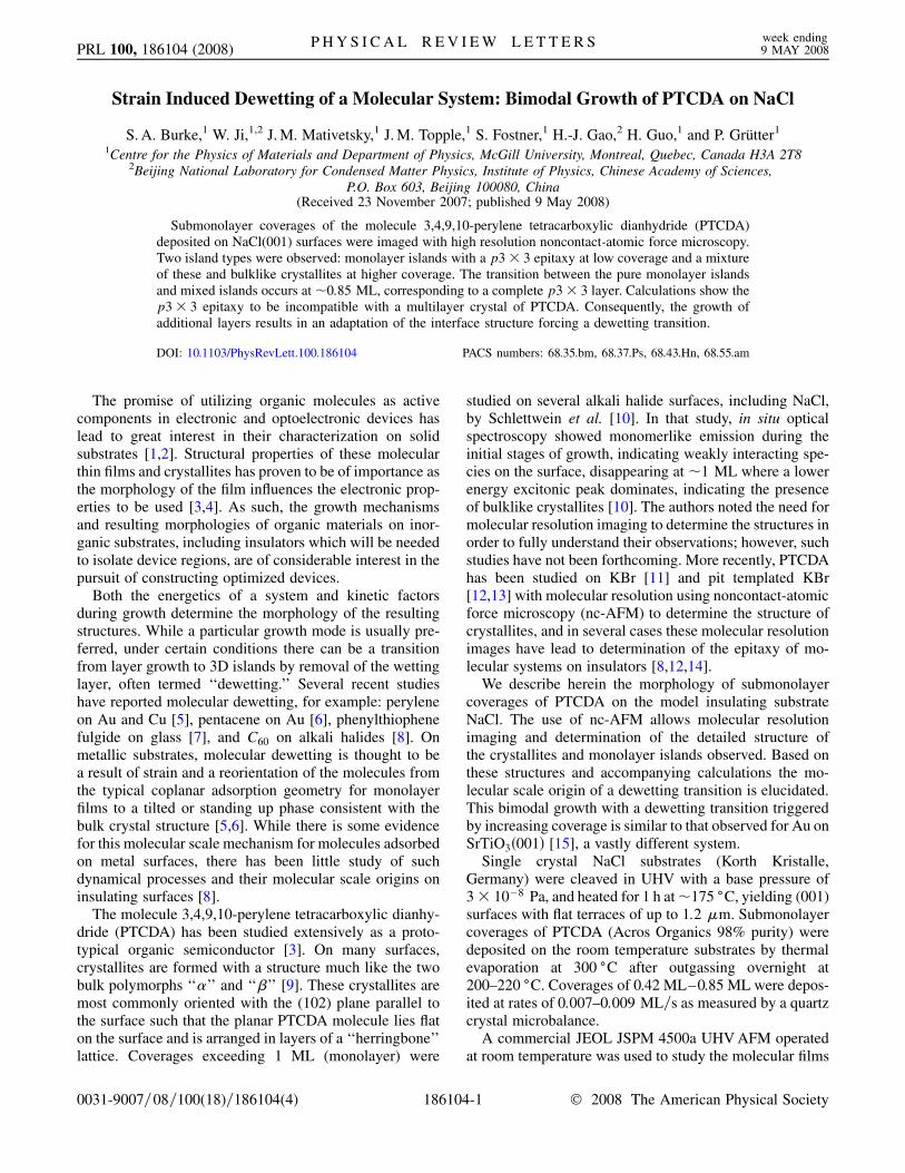
Several submonolayer coverages of PTCDA were de-posited and characterized by nc-AFM (see Fig. 1). Atcoverages of 0.74 ML and below, roughly square-shapedmonolayer islands with rounded corners showing align-ment with h110i directions of the substrate were observed.To confirm that these are indeed monolayer islands, heightswere measured with Kelvin probe feedback to compensatefor differing electrostatic forces [16] over the PTCDA andNaCl (supporting information, part 1 [17]). The height ofthe islands was found to be 3:4� 0:2 �A which correspondsclosely to the layer to layer spacing of (102) planes ofPTCDA crystals of 3.3 A [18]. At 0.85 ML, coexistence oftwo different types of islands was observed: the same
monolayer islands as described for lower coverages, andtaller islands showing crystallographic edges typical forPTCDA growth on other surfaces such as KBr [11].
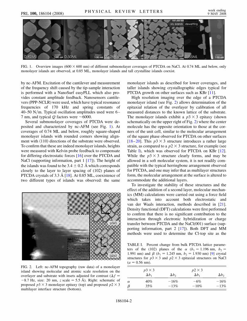
High resolution imaging over the edge of a PTCDAmonolayer island (see Fig. 2) allows determination of theepitaxial relation of the overlayer by calibration of allmeasured distances to the known lattice of the substrate.The monolayer islands exhibit a p3� 3 epitaxy (shownschematically on the upper right of Fig. 2) where the centermolecule has the opposite orientation to those at the cor-ners of the unit cell, similar to the molecular arrangementof the square phase observed for PTCDA on other surfaces[18–20]. This p3� 3 structure introduces a rather largestrain, as compared to a p2� 3 structure, for example (seeTable I), which was observed for PTCDA on KBr [12].While the p3� 3 structure clearly forms, and may beallowed in a soft molecular system, it is not readily com-patible with the typical herringbone arrangement observedfor PTCDA, and one may infer that as multilayer structuresform, the molecular arrangement at the surface is altered toaccommodate the additional layers.
To investigate the stability of these structures and theeffect of the addition of a second layer, molecular mechan-ics (MM) calculations were carried out using a force fieldwhich takes into account both electrostatic andvan der Waals interaction, methods described in [21].Density functional (DFT) calculations were first performedto confirm that there is no significant contribution to theinteraction through electronic hybridization or chargetransfer between PTCDA and the NaCl(001) surface (sup-porting information, part 2 [17]). Both DFT and MMmethods were used to determine the Cl-top site as the
FIG. 1. Overview images (600� 600 nm) of different submonolayer coverages of PTCDA on NaCl. At 0.74 ML and below, onlymonolayer islands are observed, at 0.85 ML, monolayer islands and tall crystalline islands coexist.
FIG. 2. Left: nc-AFM topography (raw data) of a monolayerisland showing molecular and atomic scale resolution on theoverlayer and substrate with insets adjusted for contrast (�f ��8:7 Hz, size: 20 nm, z scale � 5:5 �A). Right: schematic ofproposed p3� 3 monolayer epitaxy (top) and proposed p2� 3multilayer interface structure (bottom).
TABLE I. Percent change from bulk PTCDA lattice parame-ters of the (102) planes of the � (b1 � 1:196 nm, b2 �1:991 nm) and � (b1 � 1:245 nm, b2 � 1:930 nm) [9] crystalstructures for p3� 3 and p2� 3 epitaxial structures on NaCl(a � 0:56 nm).
p3� 3 p2� 3�b1 �b2 �b1 �b2
� 40% �16% �6% �16%� 35% �13% �10% �13%
PRL 100, 186104 (2008) P H Y S I C A L R E V I E W L E T T E R S week ending9 MAY 2008
186104-2
stable adsorption site, where the center of the moleculeresides over a Cl� ion. In this position, the more negativelycharged oxygen groups at the ends of the molecules resideover the Na surface ions as a result of electrostaticinteractions. Additionally, both the DFT calculations andMM calculations found molecule-substrate distancesclosely corresponding to the measured height of the mono-layer islands: 3.5 A molecule-substrate distance from DFT,and 2.73 A closest and 3.71 A farthest O-Na distancefrom MM while a layer height of 3:4� 0:2 �A was deter-mined from experiments. This good agreement betweenDFT and MM, as well as the lack of a significant electroniccontribution to the binding, allows the use of the MMmethod which can better model the intermolecular inter-actions, primarily van der Waals in origin, as well aselectrostatic interactions, shown to contribute significantlyto the molecule-substrate interaction (supporting informa-tion, part 2 [17]).
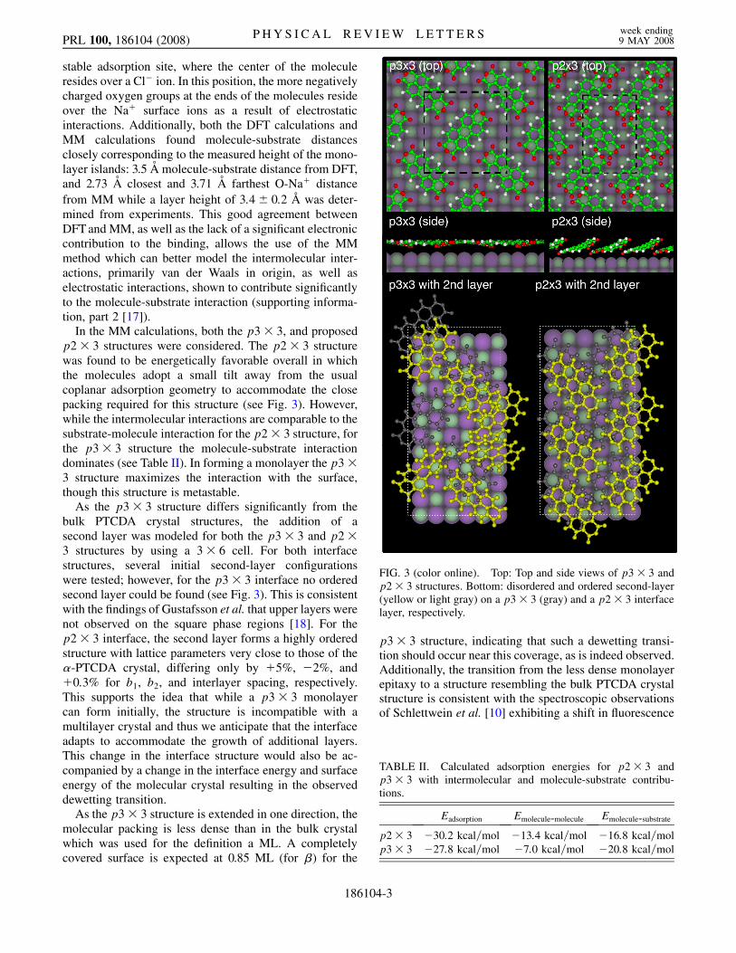
In the MM calculations, both the p3� 3, and proposedp2� 3 structures were considered. The p2� 3 structurewas found to be energetically favorable overall in whichthe molecules adopt a small tilt away from the usualcoplanar adsorption geometry to accommodate the closepacking required for this structure (see Fig. 3). However,while the intermolecular interactions are comparable to thesubstrate-molecule interaction for the p2� 3 structure, forthe p3� 3 structure the molecule-substrate interactiondominates (see Table II). In forming a monolayer the p3�3 structure maximizes the interaction with the surface,though this structure is metastable.
As the p3� 3 structure differs significantly from thebulk PTCDA crystal structures, the addition of asecond layer was modeled for both the p3� 3 and p2�3 structures by using a 3� 6 cell. For both interfacestructures, several initial second-layer configurationswere tested; however, for the p3� 3 interface no orderedsecond layer could be found (see Fig. 3). This is consistentwith the findings of Gustafsson et al. that upper layers werenot observed on the square phase regions [18]. For thep2� 3 interface, the second layer forms a highly orderedstructure with lattice parameters very close to those of the�-PTCDA crystal, differing only by 5%, �2%, and0:3% for b1, b2, and interlayer spacing, respectively.This supports the idea that while a p3� 3 monolayercan form initially, the structure is incompatible with amultilayer crystal and thus we anticipate that the interfaceadapts to accommodate the growth of additional layers.This change in the interface structure would also be ac-companied by a change in the interface energy and surfaceenergy of the molecular crystal resulting in the observeddewetting transition.
As the p3� 3 structure is extended in one direction, themolecular packing is less dense than in the bulk crystalwhich was used for the definition a ML. A completelycovered surface is expected at 0.85 ML (for �) for the
p3� 3 structure, indicating that such a dewetting transi-tion should occur near this coverage, as is indeed observed.Additionally, the transition from the less dense monolayerepitaxy to a structure resembling the bulk PTCDA crystalstructure is consistent with the spectroscopic observationsof Schlettwein et al. [10] exhibiting a shift in fluorescence
FIG. 3 (color online). Top: Top and side views of p3� 3 andp2� 3 structures. Bottom: disordered and ordered second-layer(yellow or light gray) on a p3� 3 (gray) and a p2� 3 interfacelayer, respectively.
TABLE II. Calculated adsorption energies for p2� 3 andp3� 3 with intermolecular and molecule-substrate contribu-tions.
Eadsorption Emolecule-molecule Emolecule-substrate
p2� 3 �30:2 kcal=mol �13:4 kcal=mol �16:8 kcal=molp3� 3 �27:8 kcal=mol �7:0 kcal=mol �20:8 kcal=mol
PRL 100, 186104 (2008) P H Y S I C A L R E V I E W L E T T E R S week ending9 MAY 2008
186104-3
from monomerlike signatures to bulklike excimeric signa-tures starting near 1 ML.
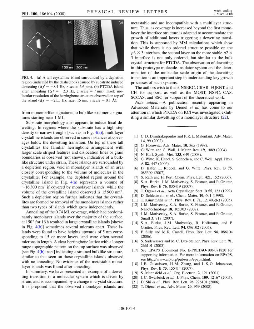
Substrate morphology also appears to induce local de-wetting. In regions where the substrate has a high stepdensity or narrow troughs [such as in Fig. 4(a)], multilayercrystalline islands are observed in some instances at cover-ages below the dewetting transition. On top of these tallcrystallites the familiar herringbone arrangement withlarger scale striped features and dislocation lines or grainboundaries is observed (not shown), indicative of a bulk-like structure under strain. These islands are surrounded bya depletion region, void in monolayer islands of an areaclosely corresponding to the volume of molecules in thecrystallite. For example, the depleted region around thecrystalline island in Fig. 4(a) represents a volume of�16 300 nm3 if covered by monolayer islands, while thevolume of the crystalline island observed is 15 900 nm3.Such a depletion region further indicates that the crystal-lites are formed by removal of the monolayer islands ratherthan two types of islands which grow independently.
Annealing of the 0.74 ML coverage, which had predomi-nantly monolayer islands over the majority of the surface,at 150� for 16 h resulted in large crystalline islands [shownin Fig. 4(b)] sometimes several microns apart. These is-lands were found to have heights upwards of 5 nm corre-sponding to 15 or more layers, and were often severalmicrons in length. A clear herringbone lattice with a longerrange topographic pattern on the top surface was observed[see Fig. 4(b) inset] indicating a strained bulklike structure,similar to that seen on those crystalline islands observedwith no annealing. No evidence of the metastable mono-layer islands was found after annealing.
In summary, we have presented an example of a dewet-ting transition in a molecular system which is driven bystrain, and is accompanied by a change in crystal structure.It is proposed that the observed monolayer islands are
metastable and are incompatible with a multilayer struc-ture. Thus, as coverage is increased beyond the first mono-layer the interface structure is adapted to accommodate thegrowth of additional layers triggering a dewetting transi-tion. This is supported by MM calculations which showthat while there is no ordered structure possible on thep3� 3 interface, the second layer on the more stable p2�3 interface is not only ordered, but similar to the bulkcrystal structure for PTCDA. The observation of dewettingin this prototype molecule-insulator system and the deter-mination of the molecular scale origin of the dewettingtransition is an important step in understanding key growthprocesses of such systems.
The authors wish to thank NSERC, CIfAR, FQRNT, andCFI for support, as well as the MOST, NSFC, CAS,SCCAS, and SSC for support of the theoretical work.
Note added.—A publication recently appearing inAdvanced Materials by Dienel et al. has come to ourattention in which PTCDA on KCl was investigated exhib-iting a similar dewettting of a monolayer structure [22].
[1] C. D. Dimitrakopoulos and P. R. L. Malenfant, Adv. Mater.14, 99 (2002).
[2] G. Horowitz, Adv. Mater. 10, 365 (1998).[3] G. Witte and C. Woll, J. Mater. Res. 19, 1889 (2004).[4] N. Karl, Synth. Met. 133, 649 (2003).[5] G. Witte, K. Hanel, S. Sohnchen, and C. Woll, Appl. Phys.
A 82, 447 (2006).[6] D. Kafer, L. Ruppel, and G. Witte, Phys. Rev. B 75,
085309 (2007).[7] S. Rath and H. Port, Chem. Phys. Lett. 421, 152 (2006).[8] S. A. Burke, J. M. Mativetsky, S. Fostner, and P. Grutter,
Phys. Rev. B 76, 035419 (2007).[9] T. Ogawa et al., Acta Crystallogr. Sect. B 55, 123 (1999).
[10] D. Schlettwein et al., Chem. Mater. 10, 601 (1998).[11] T. Kunstmann et al., Phys. Rev. B 71, 121403(R) (2005).[12] J. M. Mativetsky, S. A. Burke, S. Fostner, and P. Grutter,
Nanotechnology 18, 105303 (2007).[13] J. M. Mativetsky, S. A. Burke, S. Fostner, and P. Grutter,
Small 3, 818 (2007).[14] S. A. Burke, J. M. Mativetsky, R. Hoffmann, and P.
Grutter, Phys. Rev. Lett. 94, 096102 (2005).[15] F. Silly and M. R. Castell, Phys. Rev. Lett. 96, 086104
(2006).[16] S. Sadewasser and M. C. Lux-Steiner, Phys. Rev. Lett. 91,
266101 (2003).[17] See EPAPS Document No. E-PRLTAO-100-071820 for
supporting information. For more information on EPAPS,see http://www.aip.org/pubservs/epaps.html.
[18] J. B. Gustafsson, H. M. Zhang, and L. S. O. Johansson,Phys. Rev. B 75, 155414 (2007).
[19] S. Mannsfeld et al., Org. Electron. 2, 121 (2001).[20] J. C. Swarbrick et al., J. Phys. Chem. 109, 12167 (2005).[21] D. Shi et al., Phys. Rev. Lett. 96, 226101 (2006).[22] T. Dienel et al., Adv. Mater. 20, 959 (2008).
FIG. 4. (a) A tall crystalline island surrounded by a depletionregion (indicated by the dashed box) caused by substrate induceddewetting (�f � �8:4 Hz, z scale: 3.6 nm). (b) PTCDA islandafter annealing (�f � �2:3 Hz, z scale � 7 nm). Inset: mo-lecular resolution of the herringbone structure observed on top ofthe island (�f � �25:5 Hz, size: 15 nm, z scale � 0:1 �A).
PRL 100, 186104 (2008) P H Y S I C A L R E V I E W L E T T E R S week ending9 MAY 2008
186104-4


![Thickness-dependent spontaneous dewetting morphology of ...people.wku.edu/mikhail.khenner/LaserPattAg.pdfheterogeneous nucleation or spinodal dewetting [23]. In the case of homogeneous](https://img.pdfslide.net/doc/110x75/60ee61d71c1e3b20b84c0cd4/thickness-dependent-spontaneous-dewetting-morphology-of-heterogeneous-nucleation.jpg)


![Vocabulario bimodal[1]](https://img.pdfslide.net/doc/110x75/55b317ebbb61ebef478b46c4/vocabulario-bimodal1.jpg)