Embed Size (px)
Citation preview
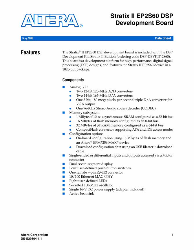
Altera Corporation DS-S29804-1.1
May 2005
Stratix II EP2S60 DSPDevelopment Board
Data Sheet
Features The Stratix® II EP2S60 DSP development board is included with the DSP Development Kit, Stratix II Edition (ordering code DSP-DEVKIT-2S60). This board is a development platform for high-performance digital signal processing (DSP) designs, and features the Stratix II EP2S60 device in a 1020-pin package.
Components
■ Analog I/O● Two 12-bit 125-MHz A/D converters● Two 14-bit 165-MHz D/A converters● One 8-bit, 180 megapixels-per-second triple D/A converter for
VGA output● One 96-KHz Stereo Audio coder/decoder (CODEC)
■ Memory subsystem● 1 MByte of 10-ns asynchronous SRAM configured as a 32-bit bus● 16 MBytes of flash memory configured as an 8-bit bus● 32 MBytes of SDRAM memory configured as a 64-bit bus● CompactFlash connector supporting ATA and IDE access modes
■ Configuration options● On-board configuration using 16 MBytes of flash memory and
an Altera® EPM7256 MAX® device● Download configuration data using an USB BlasterTM download
cable■ Single-ended or differential inputs and outputs accessed via a Mictor
connector■ Dual seven-segment display■ Four user-defined push-button switches■ One female 9-pin RS-232 connector■ 10/100 Ethernet MAC/PHY■ Eight user-defined LEDs■ Socketed 100-MHz oscillator■ Single 16-V DC power supply (adapter included)■ Active heat sink
1Preliminary

Stratix II EP2S60 DSP Development Board Data Sheet
Debugging Interfaces
■ One Mictor-type connector for Agilent and Tektronix logic analyzers■ Several 0.1-inch headers
Expansion Interfaces
■ Two connectors for Analog Devices A/D converter daughter cards■ Connector for Texas Instruments Evaluation Module (TI-EVM)
daughter cards■ Two Expansion Prototype connectors
General Description
The Stratix II EP2S60 DSP development board provides a hardware platform that designers can use to start developing DSP systems based on Stratix II devices. Combined with DSP intellectual property (IP) from Altera and Altera Megafunction Partners Program (AMPPSM) partners, users can quickly develop powerful DSP systems. Altera’s unique OpenCore® Plus technology allows users to evaluate MegaCore® functions in hardware prior to licensing them.
DSP Builder, version 5.0 includes a library for the Stratix II EP2S60 DSP development board. This library allows algorithm development, simulation, and verification on the board, all from within the MathWorks MATLAB/Simulink system-level design tool. Additionally, the Stratix II DSP development board includes a Texas Instruments’ EVM (cross-platform) daughter card connector, which enables development and verification of FPGA co-processors for off loading and accelerating compute-bound algorithms from programmable DSP processors.
2 Altera CorporationPreliminary

General Description
Components & Interfaces
Figure 1 shows a top view of the board components and interfaces.
Figure 1. Stratix II EP2S60 DSP Development Board Components & Interfaces
Note to Figure 1:(1) A TI-EVM/FPDP connector (J31, J33) is found on the reverse side of the board.
VGA Connector (J35)
Mictor Connector (J20)
External Clock Inputs (J10, J11) 9-Pin RS-232 Connector (J9)
D/A External Clock Input (J12)
8-Pin DIP Switch (SW2)
Socketed 100-MHz Oscillator (Y1)
40-Pin Connectors for AnalogDevices A/D Converters (J5, J6)
ADC A Input SMAConnector (J1)
A/D Converter Clock Selector (J3, J4)
PowerRegulator (U22)
ADC B Input SMA Connector (J2)
DAC A Output SMAConnector (J15)
DAC B Output SMAConnector (J17)
Line In (J7)
Line Out (J8)
Amplified Line OutAudio Connector
(J9)
16.0-V DC Power Supply Connector (J22)
Expansion Prototype Connector (J23, J24, J25)
Expansion Prototype Connector(J26, J27, J28)
Power Switch (SW9)
Dual Seven-segment Display (U12, U13)
Ethernet (RJ-45) Connector (RJ1)
User Push-button Switches (SW4, SW5, SW6, SW7)
CONF_DONE LED (LED5)
User LEDs (D1-D8)
Compact Flash (CON1) (on Reverse Side of Board)
D/A Converter Clock Selector (J18 , J19)
Joint Test Action Group (JTAG) Connectors (J21, J13)
Configuration-Status LEDs(LED1-LED4)
Altera Corporation 3Preliminary
Stratix II EP2S60 DSP Development Board Data Sheet
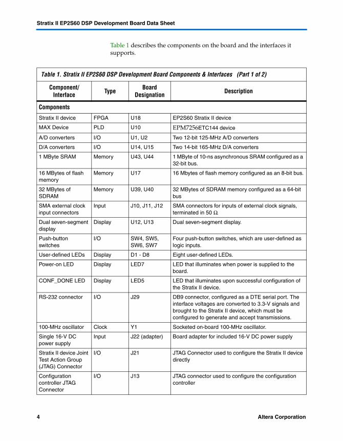
Table 1 describes the components on the board and the interfaces it supports.
Table 1. Stratix II EP2S60 DSP Development Board Components & Interfaces (Part 1 of 2)
Component/ Interface Type Board
Designation Description
Components
Stratix II device FPGA U18 EP2S60 Stratix II device
MAX Device PLD U10 EPM7256ETC144 device
A/D converters I/O U1, U2 Two 12-bit 125-MHz A/D converters
D/A converters I/O U14, U15 Two 14-bit 165-MHz D/A converters
1 MByte SRAM Memory U43, U44 1 MByte of 10-ns asynchronous SRAM configured as a 32-bit bus.
16 MBytes of flash memory
Memory U17 16 Mbytes of flash memory configured as an 8-bit bus.
32 MBytes of SDRAM
Memory U39, U40 32 MBytes of SDRAM memory configured as a 64-bit bus
SMA external clock input connectors
Input J10, J11, J12 SMA connectors for inputs of external clock signals, terminated in 50 Ω.
Dual seven-segment display
Display U12, U13 Dual seven-segment display.
Push-button switches
I/O SW4, SW5, SW6, SW7
Four push-button switches, which are user-defined as logic inputs.
User-defined LEDs Display D1 - D8 Eight user-defined LEDs.
Power-on LED Display LED7 LED that illuminates when power is supplied to the board.
CONF_DONE LED Display LED5 LED that illuminates upon successful configuration of the Stratix II device.
RS-232 connector I/O J29 DB9 connector, configured as a DTE serial port. The interface voltages are converted to 3.3-V signals and brought to the Stratix II device, which must be configured to generate and accept transmissions.
100-MHz oscillator Clock Y1 Socketed on-board 100-MHz oscillator.
Single 16-V DC power supply
Input J22 (adapter) Board adapter for included 16-V DC power supply
Stratix II device Joint Test Action Group (JTAG) Connector
I/O J21 JTAG Connector used to configure the Stratix II device directly
Configuration controller JTAG Connector
I/O J13 JTAG connector used to configure the configuration controller
4 Altera CorporationPreliminary

General Description
Environmental Requirements
The Stratix II EP2S60 DSP development board must be stored between –40° C and 100° C. The recommended operating temperature is between 0° C and 55° C.
1 The Stratix II EP2S60 DSP development board can be damaged without proper anti-static handling.
f The DSP Development Kit, Stratix II Edition includes a heat sink and fan combination, also known as an active heat sink. Depending on the specific requirements of your application, this level of cooling may not be necessary. Refer to “Install the Active Heat Sink” on page 54 for more information.
VGA D/A Converter I/O U45 One 8-bit, 180 megapixels-per-second triple D/A converter for VGA output
Audio CODEC I/O U5 96-KHz stereo audio CODEC
CompactFlash card connector
I/O CON1 CompactFlash card connector
Debugging Interfaces
Mictor connectors I/O J20 One Mictor header connected to 33 pins on the Stratix II device (32 data signals, 1 clock signal) for use with an external logic analyzer.
Expansion Interfaces
Analog Devices connector (1)
Expansion J5, J6 Interface to Analog Device’s A/D converters via two 40-pin connectors.
TI-EVM connectors Expansion J31, J33 Interface to the TI-EVM. (The connectors are on the reverse side of the board.)
Expansion Prototype Connectors
Expansion J23 - J25, J26 - J28
The board provides two custom interfaces to daughter cards via 74-pin headers. (These pins can also be used for general I/O.)
These connectors are referred to on the board as “Santa Cruz Daughter Card 1“ and “Santa Cruz Daughter Card 2”
Note to Table 1:(1) These headers can be used to interface to Analog Devices A/D converter evaluation boards. They are designated
as J5 and J6, and interface to Analog Devices AD6645/9433/9430 external A/D converters.
Table 1. Stratix II EP2S60 DSP Development Board Components & Interfaces (Part 2 of 2)
Component/ Interface Type Board
Designation Description
Altera Corporation 5Preliminary
Stratix II EP2S60 DSP Development Board Data Sheet
Using the Board When power is applied to the board and SW9 is in the "ON" position, the Power-on LED (LED7) illuminates. At that time, the MAX device (U10) programs the Stratix II device (U18) from one of 4 flash memory spaces reserved for configuration information. If configuration is successful, the CONF_DONE LED (LED5) illuminates.
1 If the Stratix II device is programmed with a design in one of the user configuration memory spaces or using the JTAG connector (J21), both the CONF_DONE LED (LED5) and the USER LED (LED1) illuminate. For more information, refer to “Configuration-Status LEDs” on page 16.
To configure the board with a new design, the designer should perform the following steps, explained in detail in this section.
1. Apply power to the board.
2. Re-configure the Stratix II device.
Apply Power
Apply power to the board by connecting the 16-V DC power supply adapter, provided in the DSP Development Kit, Stratix II edition, to the on-board power adapter connector (J22), and switching SW9 to the ON position. All of the board components draw power either directly from this 16-V supply or from the 3.3-V, 1.2-V, and 5-V regulators that are powered by the 16-V supply.
1 The 3.3-V supply provides VCCIO to the Stratix II device and all LVTTL board components. The 1.2-V supply provides VCCINT to the Stratix II device.
When power is applied to the board, the Power On LED (LED7) illuminates.
c The Stratix II EP2S60 device, the A/D and D/A converters, and power regulator U22 become hot as the board is used. Because their surface temperature may significantly increase, do not touch these devices while power is applied to the board.
6 Altera CorporationPreliminary

Non-Volatile Configuration
Configure the Stratix II Device Directly
You can configure the Stratix II device directly, without turning off power, using the Quartus® II software and the USB Blaster cable, as follows.
1. Attach the cable to J21, also labeled “JTAG Stratix II”.
2. Open a Quartus II SRAM Object File (.sof), which starts the Quartus II Programmer.
3. Select USB Blaster as the hardware.
4. Set the mode to JTAG.
5. Click Start.
After successful configuration, the CONF_DONE LED (LED5) illuminates.
f Refer to Quartus II Help for instructions on how to use the USB Blaster cable.
Non-Volatile Configuration
The designer must reconfigure the Stratix II device each time power is applied to the Stratix II DSP development board. For designers who want to power up the board and have a design immediately present in the Stratix II device, the board has a non-volatile configuration scheme. This scheme consists of a configuration controller (U10), which is an Altera EPM7256 PLD, and flash memory. The configuration controller device is non-volatile (i.e., it does not lose its configuration data when the board is powered down) and it comes factory-programmed with logic that configures the Stratix II EP2S60F1020C4 device (U18) from data stored in flash (U17) on power-up. Upon power-up, the configuration controller begins reading data from the flash memory. The flash memory, Stratix II device, and configuration controller are connected so that data from the flash configures the Stratix II device in fast passive-parallel mode.
Altera Corporation 7Preliminary
Stratix II EP2S60 DSP Development Board Data Sheet
Configuration Data
The Quartus II software can produce Hexadecimal (Intel format) Output (.hexout) files suitable for download and storage in the flash memory as configuration data. The designer can create a HEXOUT file using the Quartus II software in one of the following ways:
■ Create a HEXOUT file at the end of compilation■ Convert a SRAM Object File (.sof) to a HEXOUT file.
Write a HEXOUT file at Compilation
To set up a project so that the Quartus II software writes a HEXOUT file at the end of compilation, perform the following steps:
1. Choose Settings (Assignments menu).
2. Click Device under Compiler Settings.
3. Click Device and Pin Options.
4. Click the Programming Files tab.
5. Turn on the Hexadecimal (Intel-Format) Output File (.hexout) option. With this option turned on, the Quartus II software generates a .hexout at the end of a successful compilation.
Convert a SOF to a HEXOUT File
The designer can convert a SOF to a HEXOUT file by performing the following steps in the Quartus II software:
1. Choose Convert Programming Files (File menu).
2. Under Output programming file, choose Hexadecimal (Intel-Format) Output File for SRAM (.hexout) from the Programming file type list box.
3. Specify an output file name in the File name box. The default is output_file.hexout.
4. Click SOF Data under Input files to convert.
5. Click Add File.
6. Browse to the SOF to convert and click OK. The Quartus II software converts the file and saves the output file to the specified directory.
8 Altera CorporationPreliminary

Non-Volatile Configuration
1 Intel-format HEXOUT files contain data that is not actually written to the flash memory. The Write2Flash executable file (provided in the <installation directory>/utilities/Flash_Programmer directory) parses the HEXOUT file and creates a file with the extension .hexout.flash that contains the data to be written to flash memory. The designer can then send this file serially to the board via an RS-232 cable and write it to flash memory by the factory configuration as described in the next section.
Factory & User Configurations
The configuration controller can manage four separate Stratix II device configurations as HEXOUT data stored in flash memory: three user designs and a factory design. On power-up, the configuration controller reads one of the four (user or factory) designs from the flash memory and programs the Stratix II device accordingly. The user can select which design the Stratix II device is programmed with by setting the DIP switches on SW2.
DIP switches 1 through 3 on SW2 select one of four possible Stratix II configuration images upon power-up. When DIP switch 4 is in the “OPEN” position the configuration controller is enabled. If DIP switch 4 is in the “OPEN” position and there are no valid user-defined images, the Stratix II device is programmed with the factory configuration. Table 2 shows the DIP switch combinations used to select the available images. See “Non-Volatile Configuration” on page 7 for more details.
1 An alternative method of configuring the device with the factory design is to press push-button switch SW3.
1 Switch 4 must be set to “OPEN” to enable the configuration controller.
f To download a Quartus II-generated HEXOUT file to the flash memory on the board, refer to the Nios II Flash Programmer User Guide included on the DSP Development Kit, Stratix II Edition CD-ROM.
Table 2. Configuration DIP Switch (SW2) Combinations
Image Switch 1 Switch 2 Switch 3 Switch 4
User0 Closed Closed Closed Open
User1 Open Closed Closed Open
User2 Closed Open Closed Open
Factory Open Open Open Open
Altera Corporation 9Preliminary

Stratix II EP2S60 DSP Development Board Data Sheet
The Factory Design
When the Stratix II device is programmed with the factory design, LEDs D5 through D8 behave as a binary counter that counts down to zero. This is a power-up indication that the board is functional and the device was successfully programmed with the factory design.
Along with the LED counter, the factory design includes two blocks of IP generated by the Altera NCO Compiler. One of these oscillators is running at 10 times the frequency of the other, but both of them have the same amplitude, covering 13 bits of dynamic range. Two sine waves generated by these blocks are added together and the output is converted from a 2's complement representation into unsigned integer format. This combined sine wave signal of 14-bits dynamic range is sent to a 14-bit D/A converter.
When the analog output of the D/A converter is connected, via the included SMA cable, with the analog input of one of the 12-bit A/D converters, the A/D converter’s digital output is looped back to the Stratix II device. The design converts this loopback input from 2's complement format to unsigned integer format. The converted loopback data is captured by an instance of the SignalTap® II logic analyzer in the design for display and analysis.
f For step-by-step instructions on how to use the factory design to test the functionality of the board, refer to the DSP Development Kit, Stratix II Edition Getting Started User Guide.
10 Altera CorporationPreliminary
Non-Volatile Configuration
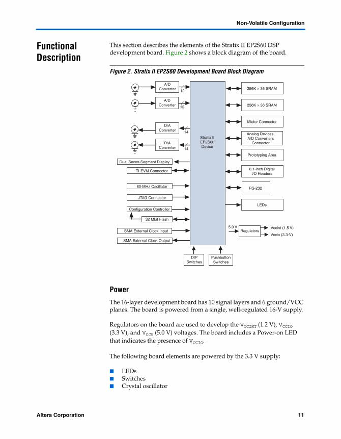
Functional Description
This section describes the elements of the Stratix II EP2S60 DSP development board. Figure 2 shows a block diagram of the board.
Figure 2. Stratix II EP2S60 Development Board Block Diagram
Power
The 16-layer development board has 10 signal layers and 6 ground/VCC planes. The board is powered from a single, well-regulated 16-V supply.
Regulators on the board are used to develop the VCCINT (1.2 V), VCCIO (3.3 V), and VCC5 (5.0 V) voltages. The board includes a Power-on LED that indicates the presence of VCCIO.
The following board elements are powered by the 3.3 V supply:
■ LEDs■ Switches■ Crystal oscillator
SMA External Clock Input
SMA External Clock Output
256K × 36 SRAM
Mictor Connector
256K × 36 SRAM
14
D/AConverter
14
D/AConverter
Stratix IIEP2S60Device
JTAG Connector
Regulators
RS-232
5.0 V Vccint (1.5 V)
Vccio (3.3-V)
80-MHz Oscillator
Prototyping Area
LEDs
PushbuttonSwitches
DIPSwitches
TI-EVM Connector
32 Mbit Flash
Analog Devices A/D Converters
Connector
Dual Seven-Segment Display
12
A/DConverter
12
A/DConverter
0.1-inch DigitalI/O Headers
Configuration Controller
Altera Corporation 11Preliminary
Stratix II EP2S60 DSP Development Board Data Sheet
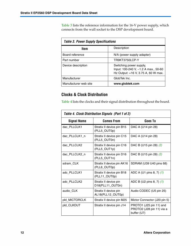
Table 3 lists the reference information for the 16-V power supply, which connects from the wall socket to the DSP development board.
Clocks & Clock Distribution
Table 4 lists the clocks and their signal distribution throughout the board.
Table 3. Power Supply Specifications
Item Description
Board reference N/A (power supply adapter)
Part number TR9KT3750LCP-Y
Device description Switching power supply, Input: 100-240 V, ~1.2 A max., 50-60 Hz Output: +16 V, 3.75 A, 60 W max.
Manufacturer GlobTek Inc.
Manufacturer web site www.globtek.com
Table 4. Clock Distribution Signals (Part 1 of 2)
Signal Name Comes From Goes To
dac_PLLCLK1 Stratix II device pin B15 (PLL5_OUT0p)
DAC A (U14 pin 28)
dac_PLLCLK1_n Stratix II device pin C15 (PLL5_OUT0n)
DAC A (U14 pin 28)
dac_PLLCLK2 Stratix II device pin C16 (PLL5_OUT1p)
DAC B (U15 pin 28) (2)
dac_PLLCLK2_n Stratix II device pin D16 (PLL5_OUT1n)
DAC B (U15 pin 28) (2)
sdram_CLK Stratix II device pin AK16 (PLL6_OUT0p)
SDRAM (U39 U40 pins 68)
adc_PLLCLK1 Stratix II device pin B18 (PLL11_OUT0p)
ADC A (U1 pins 8, 7) (1)
adc_PLLCLK2 Stratix II device pin D18(PLL11_OUT0n)
ADC B (U2 pins 8, 7) (1)
audio_CLK Stratix II device pin AL18(PLL12_OUT0p)
Audio CODEC (U5 pin 25)
pld_MICTORCLK Stratix II device pin M25 Mictor Connector (J20 pin 5)
pld_CLKOUT Stratix II device pin J14 PROTO1 (J25 pin 11) and PROTO2 (J28 pin 11) via a buffer (U7)
12 Altera CorporationPreliminary
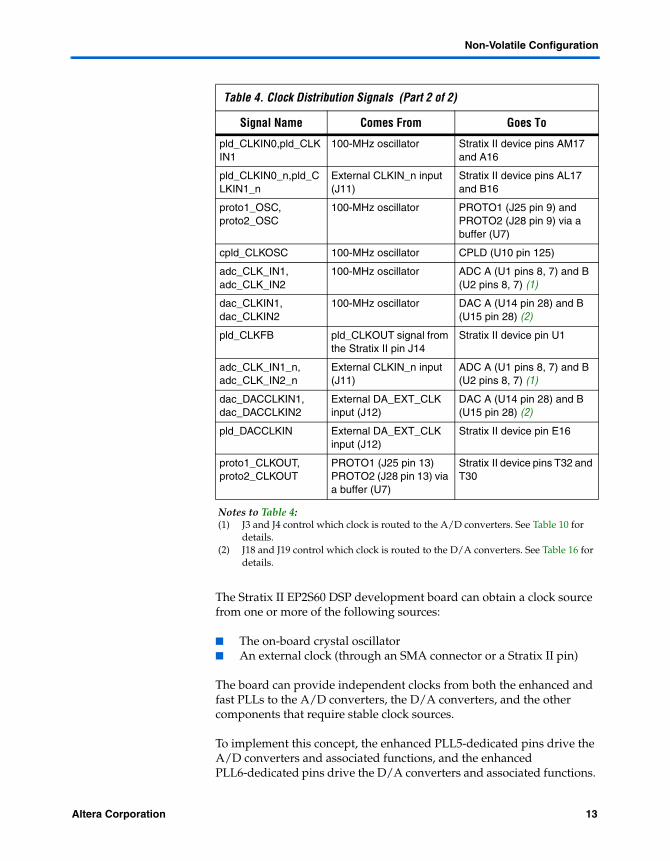
Non-Volatile Configuration
The Stratix II EP2S60 DSP development board can obtain a clock source from one or more of the following sources:
■ The on-board crystal oscillator■ An external clock (through an SMA connector or a Stratix II pin)
The board can provide independent clocks from both the enhanced and fast PLLs to the A/D converters, the D/A converters, and the other components that require stable clock sources.
To implement this concept, the enhanced PLL5-dedicated pins drive the A/D converters and associated functions, and the enhanced PLL6-dedicated pins drive the D/A converters and associated functions.
pld_CLKIN0,pld_CLKIN1
100-MHz oscillator Stratix II device pins AM17 and A16
pld_CLKIN0_n,pld_CLKIN1_n
External CLKIN_n input (J11)
Stratix II device pins AL17 and B16
proto1_OSC, proto2_OSC
100-MHz oscillator PROTO1 (J25 pin 9) and PROTO2 (J28 pin 9) via a buffer (U7)
cpld_CLKOSC 100-MHz oscillator CPLD (U10 pin 125)
adc_CLK_IN1, adc_CLK_IN2
100-MHz oscillator ADC A (U1 pins 8, 7) and B (U2 pins 8, 7) (1)
dac_CLKIN1, dac_CLKIN2
100-MHz oscillator DAC A (U14 pin 28) and B (U15 pin 28) (2)
pld_CLKFB pld_CLKOUT signal from the Stratix II pin J14
Stratix II device pin U1
adc_CLK_IN1_n, adc_CLK_IN2_n
External CLKIN_n input (J11)
ADC A (U1 pins 8, 7) and B (U2 pins 8, 7) (1)
dac_DACCLKIN1, dac_DACCLKIN2
External DA_EXT_CLK input (J12)
DAC A (U14 pin 28) and B (U15 pin 28) (2)
pld_DACCLKIN External DA_EXT_CLK input (J12)
Stratix II device pin E16
proto1_CLKOUT, proto2_CLKOUT
PROTO1 (J25 pin 13) PROTO2 (J28 pin 13) via a buffer (U7)
Stratix II device pins T32 and T30
Notes to Table 4:(1) J3 and J4 control which clock is routed to the A/D converters. See Table 10 for
details.(2) J18 and J19 control which clock is routed to the D/A converters. See Table 16 for
details.
Table 4. Clock Distribution Signals (Part 2 of 2)
Signal Name Comes From Goes To
Altera Corporation 13Preliminary

Stratix II EP2S60 DSP Development Board Data Sheet
Figure 3 is a diagram of each clock and their distribution throughout the board.
Figure 3. Clock Distribution
Table 5 lists the reference information for the 100-MHz socketed oscillator.
100-MHzOscillator
ClockDistribution
2
CLK_IN_p
CLK_IN_n
DA_EXT_CLK
ExpansionPrototypeConnector
CLKBuffer
CLKBuffer
ADC A
ADC B
DAC
DAC
ConfigurationController
SDRAM
AudioCODEC
ADC AJumper
ADC BJumper
DAC AJumper
DAC BJumper
ClockDistribution
4
ClockDistribution
3
ClockDistribution
1ExpansionPrototypeConnector
Stratix IIEP2S60F1020C4
Device
Table 5. 100-MHz Socketed Oscillator Reference
Item Description
Board reference Y1
Part number ECS-UPO-8PIN 100MHz
Device description Oscillator
Manufacturer ECS Inc.
Manufacturer web site www.ecsxtal.com
14 Altera CorporationPreliminary

Board Components
1 Clock Distribution 1 source can be either the oscillator (Y1) or an external clock inserted using J10. To use an external clock signal, remove the crystal oscillator from its socket. Make sure to note the correct orientation of the oscillator before removing it.
Board Components
The following sections describe the development board components.
Stratix II Device (U18)
The Stratix II EP2S60 device on the board features 24,176 adaptive logic modules (ALMs) in a speed grade (-4) 1020-pin FineLine BGA® package. The device has 2,544,192 total RAM bits.
f For more information on Stratix II devices, refer to the Stratix II Device Handbook.
Table 6 describes the features of the Stratix II EP2S60F1020C4 device.
Table 6. Stratix II Device Features
Feature EP2S60F1020
ALMs 24,176
Adaptive look-up tables (ALUTs) 48,352
M512 RAM Blocks (32 × 18 bits) 329
M4K RAM Blocks (128 × 36 bits) 255
M-RAM Blocks 2
Total RAM bits 2,544,192
DSP Blocks 36
Embedded multipliers (based on 18 × 18 mode of operation)
144
Enhanced PLLs 4
Fast PLLs 8
Maximum user I/O pins 717
Package type 1020-pin FineLine BGA
Board reference U18
Voltage 1.2 V (internal), 3.3 V (I/O)
Altera Corporation 15Preliminary
Stratix II EP2S60 DSP Development Board Data Sheet
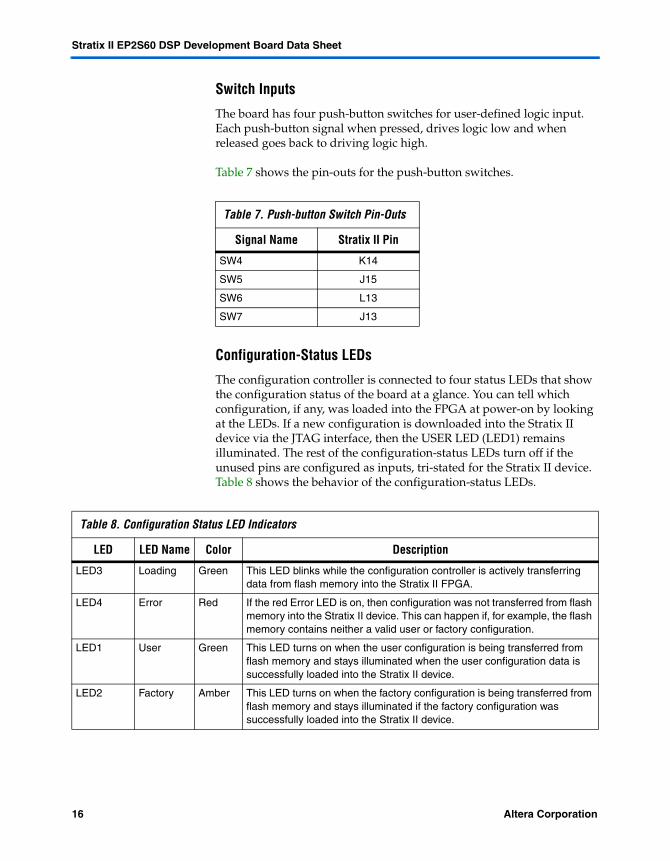
Switch Inputs
The board has four push-button switches for user-defined logic input. Each push-button signal when pressed, drives logic low and when released goes back to driving logic high.
Table 7 shows the pin-outs for the push-button switches.
Configuration-Status LEDs
The configuration controller is connected to four status LEDs that show the configuration status of the board at a glance. You can tell which configuration, if any, was loaded into the FPGA at power-on by looking at the LEDs. If a new configuration is downloaded into the Stratix II device via the JTAG interface, then the USER LED (LED1) remains illuminated. The rest of the configuration-status LEDs turn off if the unused pins are configured as inputs, tri-stated for the Stratix II device. Table 8 shows the behavior of the configuration-status LEDs.
Table 7. Push-button Switch Pin-Outs
Signal Name Stratix II Pin
SW4 K14
SW5 J15
SW6 L13
SW7 J13
Table 8. Configuration Status LED Indicators
LED LED Name Color Description
LED3 Loading Green This LED blinks while the configuration controller is actively transferring data from flash memory into the Stratix II FPGA.
LED4 Error Red If the red Error LED is on, then configuration was not transferred from flash memory into the Stratix II device. This can happen if, for example, the flash memory contains neither a valid user or factory configuration.
LED1 User Green This LED turns on when the user configuration is being transferred from flash memory and stays illuminated when the user configuration data is successfully loaded into the Stratix II device.
LED2 Factory Amber This LED turns on when the factory configuration is being transferred from flash memory and stays illuminated if the factory configuration was successfully loaded into the Stratix II device.
16 Altera CorporationPreliminary
Board Components
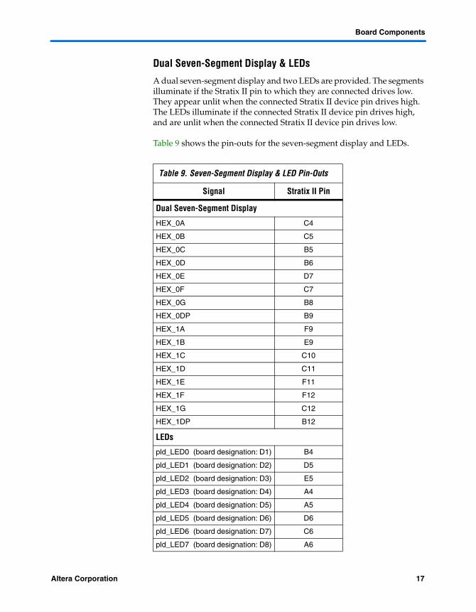
Dual Seven-Segment Display & LEDs
A dual seven-segment display and two LEDs are provided. The segments illuminate if the Stratix II pin to which they are connected drives low. They appear unlit when the connected Stratix II device pin drives high. The LEDs illuminate if the connected Stratix II device pin drives high, and are unlit when the connected Stratix II device pin drives low.
Table 9 shows the pin-outs for the seven-segment display and LEDs.
Table 9. Seven-Segment Display & LED Pin-Outs
Signal Stratix II Pin
Dual Seven-Segment Display
HEX_0A C4
HEX_0B C5
HEX_0C B5
HEX_0D B6
HEX_0E D7
HEX_0F C7
HEX_0G B8
HEX_0DP B9
HEX_1A F9
HEX_1B E9
HEX_1C C10
HEX_1D C11
HEX_1E F11
HEX_1F F12
HEX_1G C12
HEX_1DP B12
LEDs
pld_LED0 (board designation: D1) B4
pld_LED1 (board designation: D2) D5
pld_LED2 (board designation: D3) E5
pld_LED3 (board designation: D4) A4
pld_LED4 (board designation: D5) A5
pld_LED5 (board designation: D6) D6
pld_LED6 (board designation: D7) C6
pld_LED7 (board designation: D8) A6
Altera Corporation 17Preliminary
Stratix II EP2S60 DSP Development Board Data Sheet
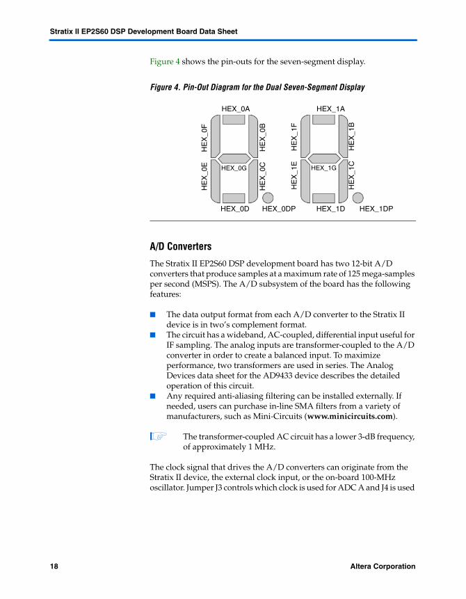
Figure 4 shows the pin-outs for the seven-segment display.
Figure 4. Pin-Out Diagram for the Dual Seven-Segment Display
A/D Converters
The Stratix II EP2S60 DSP development board has two 12-bit A/D converters that produce samples at a maximum rate of 125 mega-samples per second (MSPS). The A/D subsystem of the board has the following features:
■ The data output format from each A/D converter to the Stratix II device is in two’s complement format.
■ The circuit has a wideband, AC-coupled, differential input useful for IF sampling. The analog inputs are transformer-coupled to the A/D converter in order to create a balanced input. To maximize performance, two transformers are used in series. The Analog Devices data sheet for the AD9433 device describes the detailed operation of this circuit.
■ Any required anti-aliasing filtering can be installed externally. If needed, users can purchase in-line SMA filters from a variety of manufacturers, such as Mini-Circuits (www.minicircuits.com).
1 The transformer-coupled AC circuit has a lower 3-dB frequency, of approximately 1 MHz.
The clock signal that drives the A/D converters can originate from the Stratix II device, the external clock input, or the on-board 100-MHz oscillator. Jumper J3 controls which clock is used for ADC A and J4 is used
HEX_0A HEX_1A
HEX_0D HEX_0DP HEX_1D HEX_1DP
HE
X_0
C
HE
X_0
B
HE
X_0
E
HE
X_0
F
HEX_0G HEX_1G
HE
X_1
C
HE
X_1
B
HE
X_1
E
HE
X_1
F
18 Altera CorporationPreliminary
Board Components
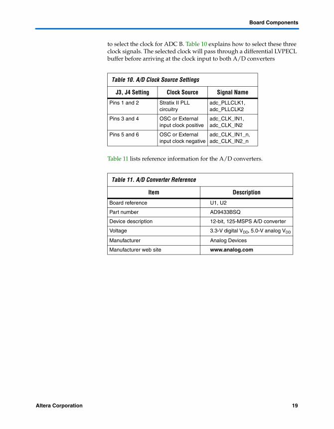
to select the clock for ADC B. Table 10 explains how to select these three clock signals. The selected clock will pass through a differential LVPECL buffer before arriving at the clock input to both A/D converters
Table 11 lists reference information for the A/D converters.
Table 10. A/D Clock Source Settings
J3, J4 Setting Clock Source Signal Name
Pins 1 and 2 Stratix II PLL circuitry
adc_PLLCLK1, adc_PLLCLK2
Pins 3 and 4 OSC or External input clock positive
adc_CLK_IN1, adc_CLK_IN2
Pins 5 and 6 OSC or External input clock negative
adc_CLK_IN1_n, adc_CLK_IN2_n
Table 11. A/D Converter Reference
Item Description
Board reference U1, U2
Part number AD9433BSQ
Device description 12-bit, 125-MSPS A/D converter
Voltage 3.3-V digital VDD, 5.0-V analog VDD
Manufacturer Analog Devices
Manufacturer web site www.analog.com
Altera Corporation 19Preliminary
Stratix II EP2S60 DSP Development Board Data Sheet
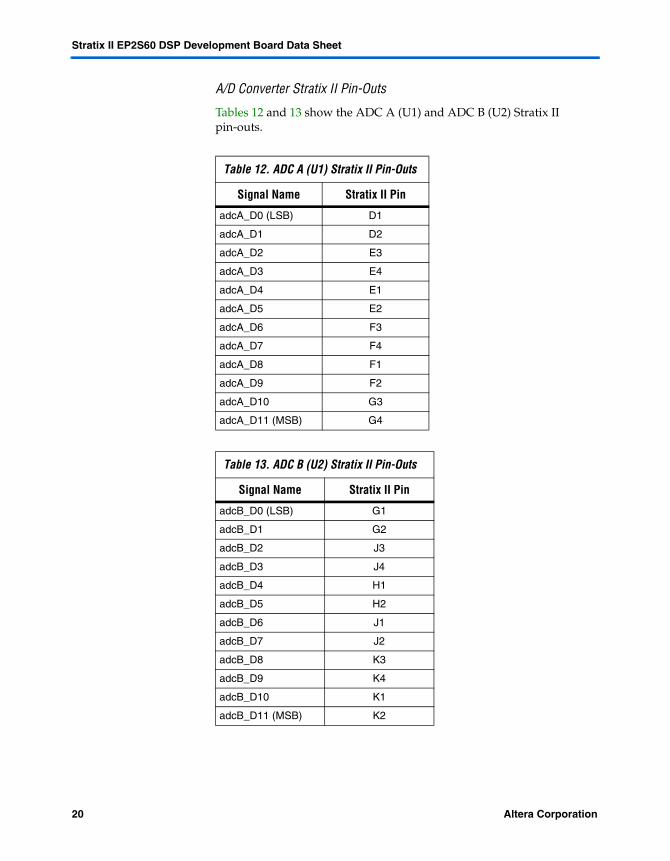
A/D Converter Stratix II Pin-Outs
Tables 12 and 13 show the ADC A (U1) and ADC B (U2) Stratix II pin-outs.
Table 12. ADC A (U1) Stratix II Pin-Outs
Signal Name Stratix II Pin
adcA_D0 (LSB) D1
adcA_D1 D2
adcA_D2 E3
adcA_D3 E4
adcA_D4 E1
adcA_D5 E2
adcA_D6 F3
adcA_D7 F4
adcA_D8 F1
adcA_D9 F2
adcA_D10 G3
adcA_D11 (MSB) G4
Table 13. ADC B (U2) Stratix II Pin-Outs
Signal Name Stratix II Pin
adcB_D0 (LSB) G1
adcB_D1 G2
adcB_D2 J3
adcB_D3 J4
adcB_D4 H1
adcB_D5 H2
adcB_D6 J1
adcB_D7 J2
adcB_D8 K3
adcB_D9 K4
adcB_D10 K1
adcB_D11 (MSB) K2
20 Altera CorporationPreliminary
Board Components
D/A Converters
The Stratix II EP2S60 DSP development board has two D/A converters. The D/A subsystem of the board has the following features:
■ The converters produce 14-bit samples at a maximum rate of 165 MSPS
■ The analog output from each D/A converter is single-ended
1 The D/A converters expect data in an unsigned integer format.
The D/A clock signals are output directly from the Stratix II device to the converters.
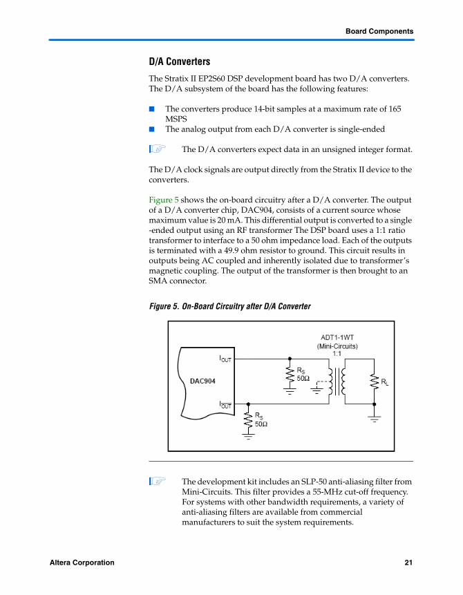
Figure 5 shows the on-board circuitry after a D/A converter. The output of a D/A converter chip, DAC904, consists of a current source whose maximum value is 20 mA. This differential output is converted to a single -ended output using an RF transformer The DSP board uses a 1:1 ratio transformer to interface to a 50 ohm impedance load. Each of the outputs is terminated with a 49.9 ohm resistor to ground. This circuit results in outputs being AC coupled and inherently isolated due to transformer’s magnetic coupling. The output of the transformer is then brought to an SMA connector.
Figure 5. On-Board Circuitry after D/A Converter
1 The development kit includes an SLP-50 anti-aliasing filter from Mini-Circuits. This filter provides a 55-MHz cut-off frequency. For systems with other bandwidth requirements, a variety of anti-aliasing filters are available from commercial manufacturers to suit the system requirements.
Altera Corporation 21Preliminary
Stratix II EP2S60 DSP Development Board Data Sheet
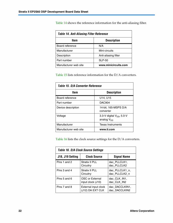
Table 14 shows the reference information for the anti-aliasing filter.
Table 15 lists reference information for the D/A converters.
Table 16 lists the clock source settings for the D/A converters.
Table 14. Anti-Aliasing Filter Reference
Item Description
Board reference N/A
Manufacturer Mini-circuits
Description Anti-aliasing filter
Part number SLP-50
Manufacturer web site www.minicircuits.com
Table 15. D/A Converter Reference
Item Description
Board reference U14, U15
Part number DAC904
Device description 14-bit, 165-MSPS D/A converter
Voltage 3.3-V digital VDD, 5.0-V analog VDD
Manufacturer Texas Instruments
Manufacturer web site www.ti.com
Table 16. D/A Clock Source Settings
J18, J19 Setting Clock Source Signal Name
Pins 1 and 2 Stratix II PLL Circuitry
dac_PLLCLK1, dac_PLLCLK2
Pins 3 and 4 Stratix II PLL Circuitry
dac_PLLCLK1_n, dac_PLLCLK2_n
Pins 5 and 6 OSC or External input clock (J10)
dac_CLK_IN1, dac_CLK_IN2
Pins 7 and 8 External input clock (J12) DA EXT CLK
dac_DACCLKIN1, dac_DACCLKIN2
22 Altera CorporationPreliminary

Board Components
D/A Converter Stratix II Pin-Outs
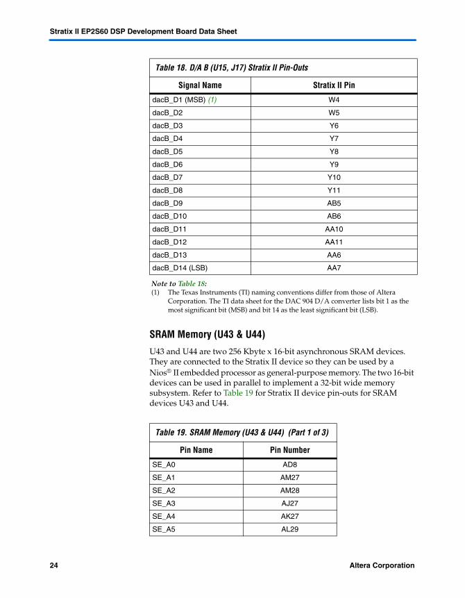
Tables 17 and 18 show the DAC A (U14) and DAC B (U15) Stratix II pin-outs.
Table 17. D/A A (U14, J15) Stratix II Pin-Outs
Signal Name Stratix II Pin
dacA_D1 (MSB) U5
dacA_D2 U6
dacA_D3 U10
dacA_D4 U11
dacA_D5 V9
dacA_D6 V10
dacA_D7 V6
dacA_D8 V7
dacA_D9 V4
dacA_D10 V5
dacA_D11 W8
dacA_D12 W9
dacA_D13 W6
dacA_D14 (LSB) W7
Altera Corporation 23Preliminary
Stratix II EP2S60 DSP Development Board Data Sheet
SRAM Memory (U43 & U44)
U43 and U44 are two 256 Kbyte x 16-bit asynchronous SRAM devices. They are connected to the Stratix II device so they can be used by a Nios® II embedded processor as general-purpose memory. The two 16-bit devices can be used in parallel to implement a 32-bit wide memory subsystem. Refer to Table 19 for Stratix II device pin-outs for SRAM devices U43 and U44.
Table 18. D/A B (U15, J17) Stratix II Pin-Outs
Signal Name Stratix II Pin
dacB_D1 (MSB) (1) W4
dacB_D2 W5
dacB_D3 Y6
dacB_D4 Y7
dacB_D5 Y8
dacB_D6 Y9
dacB_D7 Y10
dacB_D8 Y11
dacB_D9 AB5
dacB_D10 AB6
dacB_D11 AA10
dacB_D12 AA11
dacB_D13 AA6
dacB_D14 (LSB) AA7
Note to Table 18:(1) The Texas Instruments (TI) naming conventions differ from those of Altera
Corporation. The TI data sheet for the DAC 904 D/A converter lists bit 1 as the most significant bit (MSB) and bit 14 as the least significant bit (LSB).
Table 19. SRAM Memory (U43 & U44) (Part 1 of 3)
Pin Name Pin Number
SE_A0 AD8
SE_A1 AM27
SE_A2 AM28
SE_A3 AJ27
SE_A4 AK27
SE_A5 AL29
24 Altera CorporationPreliminary
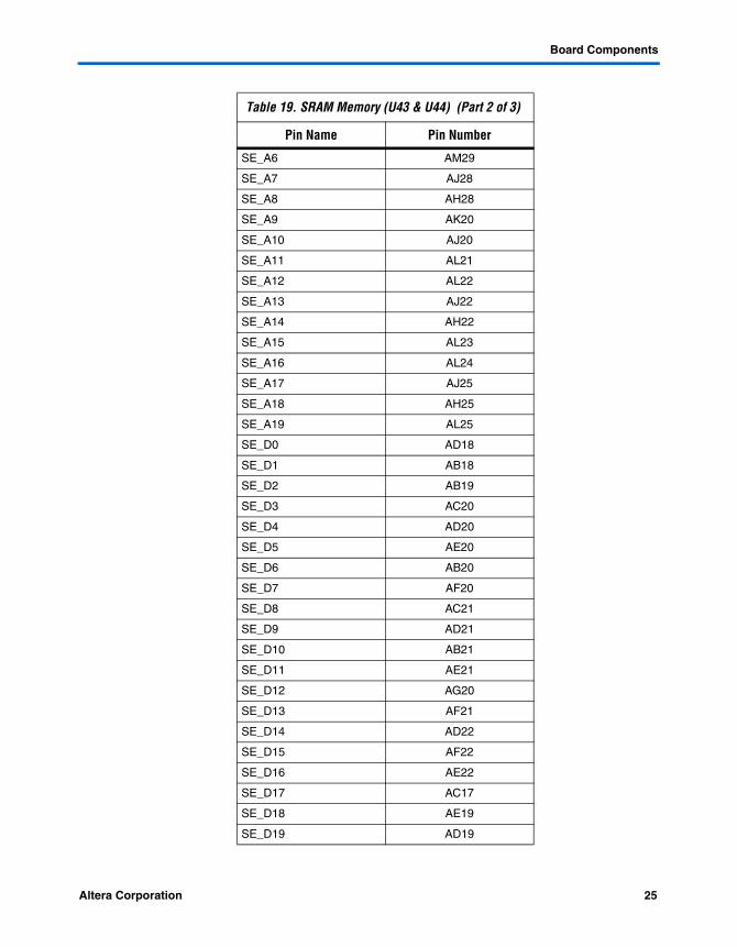
Board Components
SE_A6 AM29
SE_A7 AJ28
SE_A8 AH28
SE_A9 AK20
SE_A10 AJ20
SE_A11 AL21
SE_A12 AL22
SE_A13 AJ22
SE_A14 AH22
SE_A15 AL23
SE_A16 AL24
SE_A17 AJ25
SE_A18 AH25
SE_A19 AL25
SE_D0 AD18
SE_D1 AB18
SE_D2 AB19
SE_D3 AC20
SE_D4 AD20
SE_D5 AE20
SE_D6 AB20
SE_D7 AF20
SE_D8 AC21
SE_D9 AD21
SE_D10 AB21
SE_D11 AE21
SE_D12 AG20
SE_D13 AF21
SE_D14 AD22
SE_D15 AF22
SE_D16 AE22
SE_D17 AC17
SE_D18 AE19
SE_D19 AD19
Table 19. SRAM Memory (U43 & U44) (Part 2 of 3)
Pin Name Pin Number
Altera Corporation 25Preliminary
Stratix II EP2S60 DSP Development Board Data Sheet
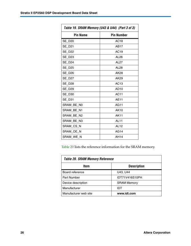
Table 20 lists the reference information for the SRAM memory.
SE_D20 AC18
SE_D21 AB17
SE_D22 AC19
SE_D23 AL26
SE_D24 AL27
SE_D25 AL28
SE_D26 AK28
SE_D27 AK29
SE_D28 AC13
SE_D29 AD10
SE_D30 AC11
SE_D31 AE11
SRAM_BE_N0 AG11
SRAM_BE_N1 AK10
SRAM_BE_N2 AK11
SRAM_BE_N3 AL11
SRAM_CS_N AL12
SRAM_OE_N AG14
SRAM_WE_N AH14
Table 20. SRAM Memory Reference
Item Description
Board reference U43, U44
Part Number IDT71V416S10PH
Device description SRAM Memory
Manufacturer IDT
Manufacturer web site www.idt.com
Table 19. SRAM Memory (U43 & U44) (Part 3 of 3)
Pin Name Pin Number
26 Altera CorporationPreliminary
Board Components
Flash Memory (U17)
U17 is a 16-Mbyte AMD AM29LV128M flash memory device connected to the Stratix II device. It can be used for two purposes:
■ A Nios II embedded processor implemented in the Stratix II device can use the flash as general-purpose readable memory and non-volatile storage.
■ The flash memory can hold a Stratix II device configuration file that is used by the configuration controller to load the Stratix II device at power-up.
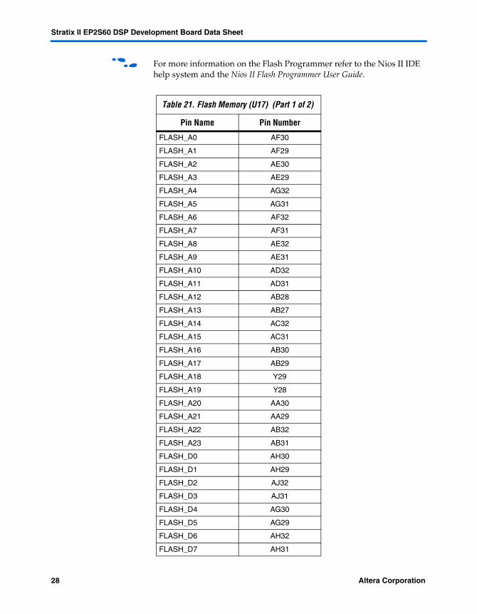
Refer to Table 21 for Stratix II pin-outs for flash memory device U17.
Hardware configuration data that implements the sines reference design is prestored in this flash memory and configures the Stratix II device with this design on boot up. A Nios II reference design can identify the 16-Mbyte flash memory in its address space, and can program new data (either new Stratix II configuration data, Nios II embedded processor software, or both) into flash memory. The Nios II integrated development environment (IDE) provides a Flash Programmer feature, which you can use to program flash memory. Altera also provides Nios II routines for writing and erasing flash memory. To program or erase flash memory, you need to install the Nios II development tools from the Nios II Embedded Processor Windows, version 5.0 CD-ROM included in your kit, and use the Nios II IDE Flash Programmer. To use the Flash Programmer with the DSP board, you must specify an SOPC Builder setting that locates a board description file for the DSP board. Perform the following:
1. Start the Quartus II software.
a. Choose Tools > SOPC Builder... to start SOPC Builder from the Quartus II software.
b. In SOPC Builder choose File->SOPC Builder Setup
c. In the Componet/Kit Library Search Path enter the path to the Stratix II DSP board component. Use "+" to delineate multiple paths. Specify the following path:
C:\altera\kits\StratixII_DSP_Kit-v1.1.0\Examples\HW\NiosII
Altera Corporation 27Preliminary
Stratix II EP2S60 DSP Development Board Data Sheet
f For more information on the Flash Programmer refer to the Nios II IDE help system and the Nios II Flash Programmer User Guide.
Table 21. Flash Memory (U17) (Part 1 of 2)
Pin Name Pin Number
FLASH_A0 AF30
FLASH_A1 AF29
FLASH_A2 AE30
FLASH_A3 AE29
FLASH_A4 AG32
FLASH_A5 AG31
FLASH_A6 AF32
FLASH_A7 AF31
FLASH_A8 AE32
FLASH_A9 AE31
FLASH_A10 AD32
FLASH_A11 AD31
FLASH_A12 AB28
FLASH_A13 AB27
FLASH_A14 AC32
FLASH_A15 AC31
FLASH_A16 AB30
FLASH_A17 AB29
FLASH_A18 Y29
FLASH_A19 Y28
FLASH_A20 AA30
FLASH_A21 AA29
FLASH_A22 AB32
FLASH_A23 AB31
FLASH_D0 AH30
FLASH_D1 AH29
FLASH_D2 AJ32
FLASH_D3 AJ31
FLASH_D4 AG30
FLASH_D5 AG29
FLASH_D6 AH32
FLASH_D7 AH31
28 Altera CorporationPreliminary
Board Components
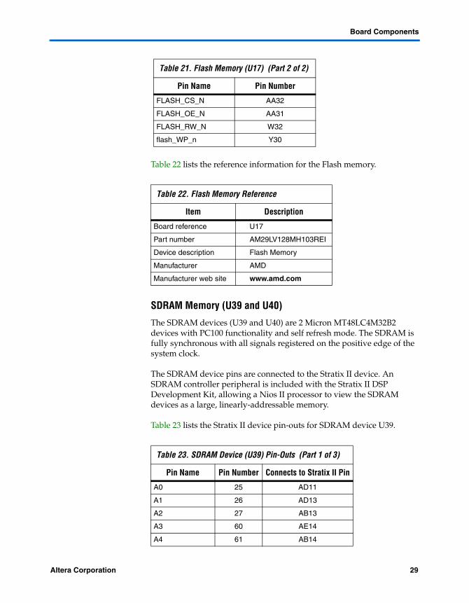
Table 22 lists the reference information for the Flash memory.
SDRAM Memory (U39 and U40)
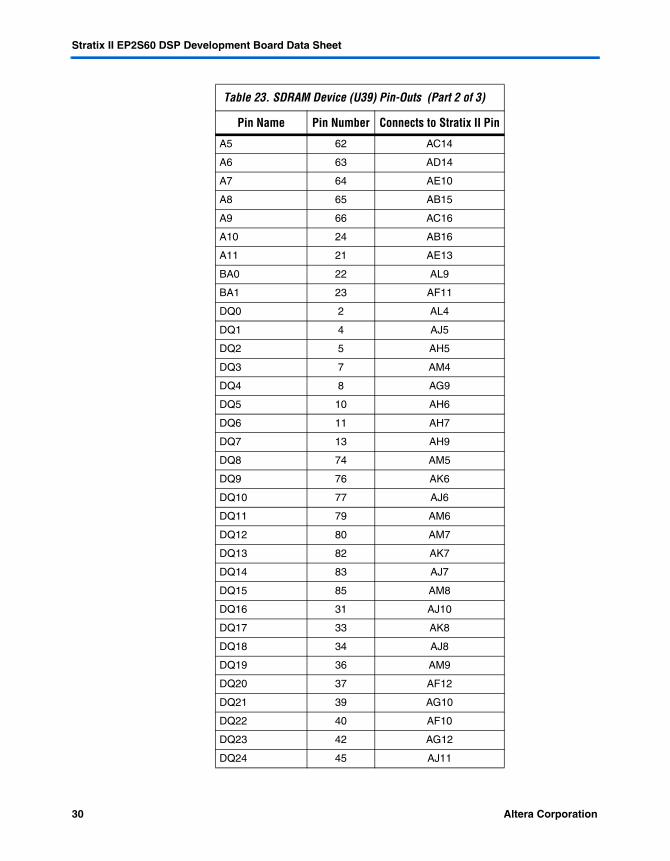
The SDRAM devices (U39 and U40) are 2 Micron MT48LC4M32B2 devices with PC100 functionality and self refresh mode. The SDRAM is fully synchronous with all signals registered on the positive edge of the system clock.
The SDRAM device pins are connected to the Stratix II device. An SDRAM controller peripheral is included with the Stratix II DSP Development Kit, allowing a Nios II processor to view the SDRAM devices as a large, linearly-addressable memory.
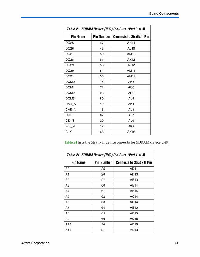
Table 23 lists the Stratix II device pin-outs for SDRAM device U39.
FLASH_CS_N AA32
FLASH_OE_N AA31
FLASH_RW_N W32
flash_WP_n Y30
Table 21. Flash Memory (U17) (Part 2 of 2)
Pin Name Pin Number
Table 22. Flash Memory Reference
Item Description
Board reference U17
Part number AM29LV128MH103REI
Device description Flash Memory
Manufacturer AMD
Manufacturer web site www.amd.com
Table 23. SDRAM Device (U39) Pin-Outs (Part 1 of 3)
Pin Name Pin Number Connects to Stratix II Pin
A0 25 AD11
A1 26 AD13
A2 27 AB13
A3 60 AE14
A4 61 AB14
Altera Corporation 29Preliminary
Stratix II EP2S60 DSP Development Board Data Sheet
A5 62 AC14
A6 63 AD14
A7 64 AE10
A8 65 AB15
A9 66 AC16
A10 24 AB16
A11 21 AE13
BA0 22 AL9
BA1 23 AF11
DQ0 2 AL4
DQ1 4 AJ5
DQ2 5 AH5
DQ3 7 AM4
DQ4 8 AG9
DQ5 10 AH6
DQ6 11 AH7
DQ7 13 AH9
DQ8 74 AM5
DQ9 76 AK6
DQ10 77 AJ6
DQ11 79 AM6
DQ12 80 AM7
DQ13 82 AK7
DQ14 83 AJ7
DQ15 85 AM8
DQ16 31 AJ10
DQ17 33 AK8
DQ18 34 AJ8
DQ19 36 AM9
DQ20 37 AF12
DQ21 39 AG10
DQ22 40 AF10
DQ23 42 AG12
DQ24 45 AJ11
Table 23. SDRAM Device (U39) Pin-Outs (Part 2 of 3)
Pin Name Pin Number Connects to Stratix II Pin
30 Altera CorporationPreliminary
Board Components
Table 24 lists the Stratix II device pin-outs for SDRAM device U40.
DQ25 47 AH11
DQ26 48 AL10
DQ27 50 AM10
DQ28 51 AK12
DQ29 53 AJ12
DQ30 54 AM11
DQ31 56 AM12
DQM0 16 AK5
DQM1 71 AG8
DQM2 28 AH8
DQM3 59 AL5
RAS_N 19 AK4
CAS_N 18 AL8
CKE 67 AL7
CS_N 20 AL6
WE_N 17 AK9
CLK 68 AK16
Table 24. SDRAM Device (U40) Pin-Outs (Part 1 of 3)
Pin Name Pin Number Connects to Stratix II Pin
A0 25 AD11
A1 26 AD13
A2 27 AB13
A3 60 AE14
A4 61 AB14
A5 62 AC14
A6 63 AD14
A7 64 AE10
A8 65 AB15
A9 66 AC16
A10 24 AB16
A11 21 AE13
Table 23. SDRAM Device (U39) Pin-Outs (Part 3 of 3)
Pin Name Pin Number Connects to Stratix II Pin
Altera Corporation 31Preliminary

Stratix II EP2S60 DSP Development Board Data Sheet
BA0 22 AL9
BA1 23 AF11
DQ0 2 AH13
DQ1 4 AG13
DQ2 5 AF13
DQ3 7 AG15
DQ4 8 AL14
DQ5 10 AJ14
DQ6 11 AJ13
DQ7 13 AM14
DQ8 74 AL20
DQ9 76 AH19
DQ10 77 AJ19
DQ11 79 AH20
DQ12 80 AM21
DQ13 82 AK21
DQ14 83 AJ21
DQ15 85 AM22
DQ16 31 AJ23
DQ17 33 AK22
DQ18 34 AG22
DQ19 36 AG23
DQ20 37 AM23
DQ21 39 AK23
DQ22 40 AK24
DQ23 42 AM24
DQ24 45 AK25
DQ25 47 AH24
DQ26 48 AH26
DQ27 50 AG24
DQ28 51 AM26
DQ29 53 AM25
DQ30 54 AJ26
DQ31 56 AK26
Table 24. SDRAM Device (U40) Pin-Outs (Part 2 of 3)
Pin Name Pin Number Connects to Stratix II Pin
32 Altera CorporationPreliminary

Board Components
Table 25 lists the reference information for the SDRAM memory.
DQM0 16 AK13
DQM1 71 AL13
DQM2 28 AB12
DQM3 59 AC12
RAS_N 19 AK4
CAS_N 18 AL8
CKE 67 AL7
CS_N 20 AL6
Table 25. SDRAM Memory Reference
Item Description
Board reference U39, U40
Part number MT48LC4M32B2TG-7
Device description SDRAM Memory
Manufacturer Micron
Manufacturer web site www.micron.com
Table 24. SDRAM Device (U40) Pin-Outs (Part 3 of 3)
Pin Name Pin Number Connects to Stratix II Pin
Altera Corporation 33Preliminary

Stratix II EP2S60 DSP Development Board Data Sheet
Ethernet MAC/PHY (U16)
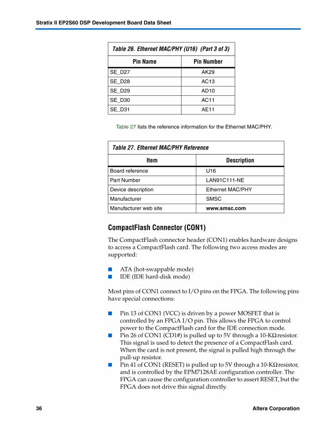
The LAN91C111 (U16) is a mixed signal analog/digital device that implements protocols at 10 Mbps and 100 Mbps. The control pins of U16 are connected to the Stratix II device so that user logic (e.g., the Nios II processor) can access Ethernet via the RJ-45 connector (RJ1). Refer to Table 26 for Stratix II pin-outs for Ethernet MAC/PHY device U16.t
Table 26. Ethernet MAC/PHY (U16) (Part 1 of 3)
Pin Name Pin Number
ENET_ADS_N AA25
ENET_AEN AC25
ENET_BE_N0 AE26
ENET_BE_N1 AE25
ENET_BE_N2 AD25
ENET_BE_N3 AD24
ENET_DATACS_N T20
ENET_INTRQ0 AB23
ENET_IOCHRDY V26
ENET_IOR_N AC24
ENET_IOW_N AB26
ENET_LDEV_N T26
enet_RESET_n
ENET_SRDY_N T25
ENET_W_R_N T21
SE_A0 AD8
SE_A1 AM27
SE_A2 AM28
SE_A3 AJ27
SE_A4 AK27
SE_A5 AL29
SE_A6 AM29
SE_A7 AJ28
SE_A8 AH28
SE_A9 AK20
SE_A10 AJ20
SE_A11 AL21
SE_A12 AL22
34 Altera CorporationPreliminary

Board Components
SE_A13 AJ22
SE_A14 AH22
SE_A15 AL23
SE_A16 AL24
SE_A17 AJ25
SE_A18 AH25
SE_A19 AL25
SE_D0 AD18
SE_D1 AB18
SE_D2 AB19
SE_D3 AC20
SE_D4 AD20
SE_D5 AE20
SE_D6 AB20
SE_D7 AF20
SE_D8 AC21
SE_D9 AD21
SE_D10 AB21
SE_D11 AE21
SE_D12 AG20
SE_D13 AF21
SE_D14 AD22
SE_D15 AF22
SE_D16 AE22
SE_D17 AC17
SE_D18 AE19
SE_D19 AD19
SE_D20 AC18
SE_D21 AB17
SE_D22 AC19
SE_D23 AL26
SE_D24 AL27
SE_D25 AL28
SE_D26 AK28
Table 26. Ethernet MAC/PHY (U16) (Part 2 of 3)
Pin Name Pin Number
Altera Corporation 35Preliminary
Stratix II EP2S60 DSP Development Board Data Sheet
Table 27 lists the reference information for the Ethernet MAC/PHY.
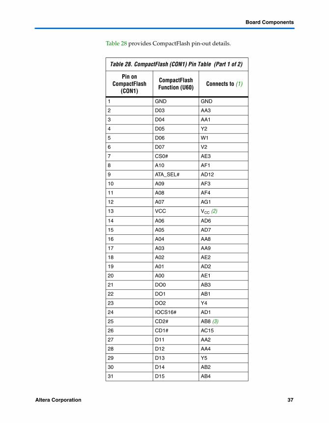
CompactFlash Connector (CON1)
The CompactFlash connector header (CON1) enables hardware designs to access a CompactFlash card. The following two access modes are supported:
■ ATA (hot-swappable mode)■ IDE (IDE hard-disk mode)
Most pins of CON1 connect to I/O pins on the FPGA. The following pins have special connections:
■ Pin 13 of CON1 (VCC) is driven by a power MOSFET that is controlled by an FPGA I/O pin. This allows the FPGA to control power to the CompactFlash card for the IDE connection mode.
■ Pin 26 of CON1 (CD1#) is pulled up to 5V through a 10-KΩ resistor. This signal is used to detect the presence of a CompactFlash card. When the card is not present, the signal is pulled high through the pull-up resistor.
■ Pin 41 of CON1 (RESET) is pulled up to 5V through a 10-KΩ resistor, and is controlled by the EPM7128AE configuration controller. The FPGA can cause the configuration controller to assert RESET, but the FPGA does not drive this signal directly.
SE_D27 AK29
SE_D28 AC13
SE_D29 AD10
SE_D30 AC11
SE_D31 AE11
Table 27. Ethernet MAC/PHY Reference
Item Description
Board reference U16
Part Number LAN91C111-NE
Device description Ethernet MAC/PHY
Manufacturer SMSC
Manufacturer web site www.smsc.com
Table 26. Ethernet MAC/PHY (U16) (Part 3 of 3)
Pin Name Pin Number
36 Altera CorporationPreliminary
Board Components
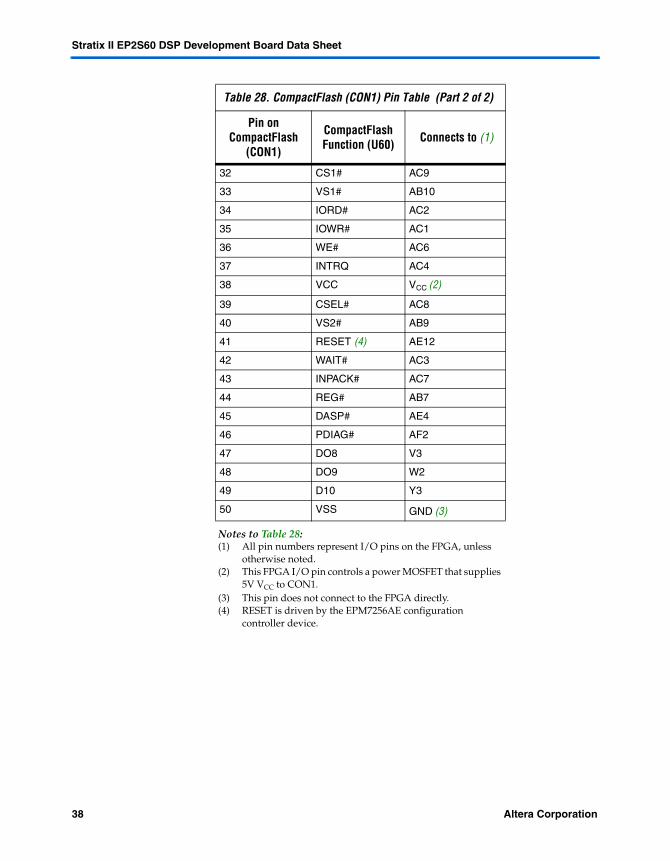
Table 28 provides CompactFlash pin-out details.
Table 28. CompactFlash (CON1) Pin Table (Part 1 of 2)
Pin on CompactFlash
(CON1)
CompactFlash Function (U60) Connects to (1)
1 GND GND
2 D03 AA3
3 D04 AA1
4 D05 Y2
5 D06 W1
6 D07 V2
7 CS0# AE3
8 A10 AF1
9 ATA_SEL# AD12
10 A09 AF3
11 A08 AF4
12 A07 AG1
13 VCC VCC (2)
14 A06 AD6
15 A05 AD7
16 A04 AA8
17 A03 AA9
18 A02 AE2
19 A01 AD2
20 A00 AE1
21 DO0 AB3
22 DO1 AB1
23 DO2 Y4
24 IOCS16# AD1
25 CD2# AB8 (3)
26 CD1# AC15
27 D11 AA2
28 D12 AA4
29 D13 Y5
30 D14 AB2
31 D15 AB4
Altera Corporation 37Preliminary
Stratix II EP2S60 DSP Development Board Data Sheet
32 CS1# AC9
33 VS1# AB10
34 IORD# AC2
35 IOWR# AC1
36 WE# AC6
37 INTRQ AC4
38 VCC VCC (2)
39 CSEL# AC8
40 VS2# AB9
41 RESET (4) AE12
42 WAIT# AC3
43 INPACK# AC7
44 REG# AB7
45 DASP# AE4
46 PDIAG# AF2
47 DO8 V3
48 DO9 W2
49 D10 Y3
50 VSS GND (3)
Notes to Table 28:(1) All pin numbers represent I/O pins on the FPGA, unless
otherwise noted.(2) This FPGA I/O pin controls a power MOSFET that supplies
5V VCC to CON1.(3) This pin does not connect to the FPGA directly.(4) RESET is driven by the EPM7256AE configuration
controller device.
Table 28. CompactFlash (CON1) Pin Table (Part 2 of 2)
Pin on CompactFlash
(CON1)
CompactFlash Function (U60) Connects to (1)
38 Altera CorporationPreliminary

Board Components
Table 29 lists the reference information for the CompactFlash connector.
f For general information on CompactFlash, see www.compactflash.org.
Mictor Connector (J20)
The Mictor connector (J20) can be used to transmit up to 27 high-speed I/O signals with very low noise via a shielded Mictor cable. J20 is used as a debug port. Twenty-five of the Mictor connector signals are used as data, and two signals are used as clock input and clock output.
Most pins on J20 connect to I/O pins on the Stratix II device (U18). For systems that do not use the Mictor connector for debugging the Nios II processor, any on-chip signals can be routed to I/O pins and probed at J20 via a Mictor cable. External scopes and logic analyzers can connect to J20 and analyze a large number of signals simultaneously.
f For details on Nios II debugging products that use the Mictor connector, see www.altera.com.
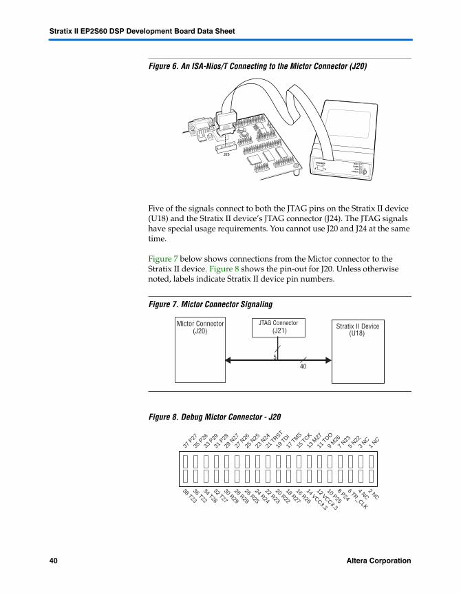
Figure 6 shows an example of an in-target system analyzer ISA-Nios/T (sold separately) by First Silicon Solutions (FS2) Inc. connected to the Mictor connector. For details see www.fs2.com.
Table 29. CompactFlash Connector Reference
Item Description
Board reference CON1
Part Number 53856-5010
Device description CompactFlash connector
Manufacturer Molex
Manufacturer web site www.molex.com
Altera Corporation 39Preliminary
Stratix II EP2S60 DSP Development Board Data Sheet
Figure 6. An ISA-Nios/T Connecting to the Mictor Connector (J20)
Five of the signals connect to both the JTAG pins on the Stratix II device (U18) and the Stratix II device’s JTAG connector (J24). The JTAG signals have special usage requirements. You cannot use J20 and J24 at the same time.
Figure 7 below shows connections from the Mictor connector to the Stratix II device. Figure 8 shows the pin-out for J20. Unless otherwise noted, labels indicate Stratix II device pin numbers.
Figure 7. Mictor Connector Signaling
Figure 8. Debug Mictor Connector - J20
BUSYCOMM
RUNPOWER
1
J25
(J20) (U18)Stratix II Device
40
JTAG Connector(J21)
5
Mictor Connector
38 T23
37 P
27
36 T22
35 P
26
34 T28
33 P
29
32 T27
31 P
28
30 R29
29 N
27
28 R28
27 N
26
26 R25
25 N
25
24 R24
23 N
24
22 R23
21 T
RST
20 R22
19 T
DI
18 R27
17 T
MS
16 R26
15 T
CK
14 VCC3.3
13 M
27
12 VCC3.3
11 T
DO
10 P25
9 M
26
8 P24
7 N23
6 TR_CLK
5 N22
4 NC
3 NC
2 NC
1 NC
40 Altera CorporationPreliminary
Board Components
Table 30 lists the reference information for the Mictor connector.
VGA Interface (J35)
The board contains a high density DP15 connector, which outputs VGA, as well as a Triple Video D/A converter which has the following features:
■ 3 x 8 bit, 180 megapixels per second■ ±2.5% gain matching■ ±0.5 LSB linearity error■ Internal bandgap voltage reference■ Low glitch energy■ Single 3.3-V power supply
Table 31 shows the pin-outs for the VGA interface.
Table 30. Mictor Connector Reference
Item Description
Board reference J20
Part number 2-767004-2
Device description Mictor connector
Manufacturer Tyco
Manufacturer web site www.tyco.com
Table 31. VGA Interface (U45, J35) Pin-Outs (Part 1 of 2)
Signal Stratix II Pin
vga_B0 B7
vga_B1 E7
vga_B2 E6
vga_B3 A7
vga_B4 C9
vga_B5 A8
vga_B6 C8
vga_B7 A9
vga_G0 E11
vga_G1 G10
vga_G2 G11
vga_G3 G12
Altera Corporation 41Preliminary
Stratix II EP2S60 DSP Development Board Data Sheet
Table 32 describes the device used to implement the VGA interface.
vga_G4 D12
vga_G5 A11
vga_G6 B11
vga_G7 A12
vga_R0 D8
vga_R1 E8
vga_R2 F8
vga_R3 F10
vga_R4 A10
vga_R5 B10
vga_R6 D10
vga_R7 D11
vga_BLANK_n G13
vga_CLOCK E13
vga_HSYNC F15
vga_VSYNC B14
vga_SYNC_n F13
Table 32. VGA Interface Device Reference
Item Description
Board reference U45
Part number FMS3818KRC
Device description Triple Video D/A Converter
Voltage 3.3 V
Manufacturer Fairchild
Manufacturer web site www.fairchildsemi.com
Table 31. VGA Interface (U45, J35) Pin-Outs (Part 2 of 2)
Signal Stratix II Pin
42 Altera CorporationPreliminary

Expansion Interfaces
Audio CODEC (U5)
The board contains three stereo jack connectors, which serve as one stereo input, one amplified stereo output and one non-amplified stereo output. The stereo jacks are driven by a Stereo Audio CODEC running at 8-96 KHz. Table 33 shows the pin-outs for the CODEC.
Table 34 describes the device used to implement the CODEC.
Expansion Interfaces
The Stratix II EP2S60 DSP development board includes the following interfaces:
■ A TI-EVM/FPDP connector (J31, J33), located on the reverse side of the board
■ An RS-232C Serial I/O interface (J29)
Table 33. Audio CODEC (U5) Pin-Outs
Signal Stratix II Pin
audio_BCLK AG4
audio_CS_n AH1
audio_SDIN AH2
audio_SCLK AH3
audio_MODE AH4
audio_DOUT AJ1
audio_DIN AJ2
audio_LRCIN AG2
audio_LRCOUT AG3
audio_CLK AL18
Table 34. Audio CODEC Device Reference
Item Description
Board reference U5
Part number TLV320AIC23PW
Device description Stereo Audio CODEC, 8-96 KHz
Voltage 3.3 V
Manufacturer Texas Instruments
Manufacturer web site www.ti.com
Altera Corporation 43Preliminary
Stratix II EP2S60 DSP Development Board Data Sheet
■ Two 0.1-inch headers specifically designed to be used with external analog-to-digital devices made by Analog Devices Corporation (J6, J5)
■ Two Altera Expansion Prototype Connectors (J23, J24, J25; J26, J27, J28)
TI-EVM/FPDP Connector (J31, J33)
The TI-EVM interface is specifically designed to work with TI boards that have the EVM interface. Refer to the Texas Instruments web site for details on which of their boards feature this connector.
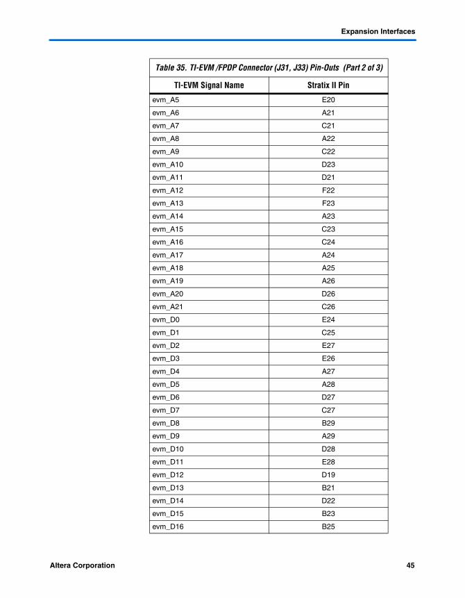
Table 35 lists the pin-outs for the TI-EVM and FPDP connectors.
Table 35. TI-EVM /FPDP Connector (J31, J33) Pin-Outs (Part 1 of 3)
TI-EVM Signal Name Stratix II Pin
J31
evm_DX0 J21
evm_DR0 H22
evm_IAK K12
evm_INUM0 H13
evm_CNTL0 L12
evm_STAT0 J12
evm_DMAC0 H12
evm_CLKOUT2 K11
evm_CLKX0 J22
evm_FSX0 G22
evm_CLKR0 K22
evm_FSR0 K21
evm_RESET J11
evm_INT0 H11
evm_INT1 L14
evm_INT2 C13
evm_INT3 B13
J33
evm_A2 B20
evm_A3 E19
evm_A4 C20
44 Altera CorporationPreliminary
Expansion Interfaces
evm_A5 E20
evm_A6 A21
evm_A7 C21
evm_A8 A22
evm_A9 C22
evm_A10 D23
evm_A11 D21
evm_A12 F22
evm_A13 F23
evm_A14 A23
evm_A15 C23
evm_A16 C24
evm_A17 A24
evm_A18 A25
evm_A19 A26
evm_A20 D26
evm_A21 C26
evm_D0 E24
evm_D1 C25
evm_D2 E27
evm_D3 E26
evm_D4 A27
evm_D5 A28
evm_D6 D27
evm_D7 C27
evm_D8 B29
evm_D9 A29
evm_D10 D28
evm_D11 E28
evm_D12 D19
evm_D13 B21
evm_D14 D22
evm_D15 B23
evm_D16 B25
Table 35. TI-EVM /FPDP Connector (J31, J33) Pin-Outs (Part 2 of 3)
TI-EVM Signal Name Stratix II Pin
Altera Corporation 45Preliminary

Stratix II EP2S60 DSP Development Board Data Sheet
RS-232C Serial I/O Interface
The board contains a DB9 connector (J29), which provides a bidirectional RS-232C serial I/O interface. The board contains the transceiver (U41), however the logic controller (UART) must be implemented in the Stratix II device. Table 37 describes the device used to implement the RS-232C interface.
evm_D17 D25
evm_D18 B27
evm_D19 C28
evm_D20 D20
evm_D21 B22
evm_D22 E22
evm_D23 B24
evm_D24 B26
evm_D25 E25
evm_D26 B28
evm_D27 C29
evm_D28 L21
evm_D29 G21
evm_D30 L18
evm_D31 J19
evm_BE_n0 H20
evm_BE_n1 L19
evm_BE_n2 K19
evm_BE_n3 G20
evm_AWE_n L20
evm_ARDY H21
evm_ACE2_n J20
evm_ARE_n K20
evm_AOE_n K18
evm_ACE3_n E14
Table 35. TI-EVM /FPDP Connector (J31, J33) Pin-Outs (Part 3 of 3)
TI-EVM Signal Name Stratix II Pin
46 Altera CorporationPreliminary
Expansion Interfaces
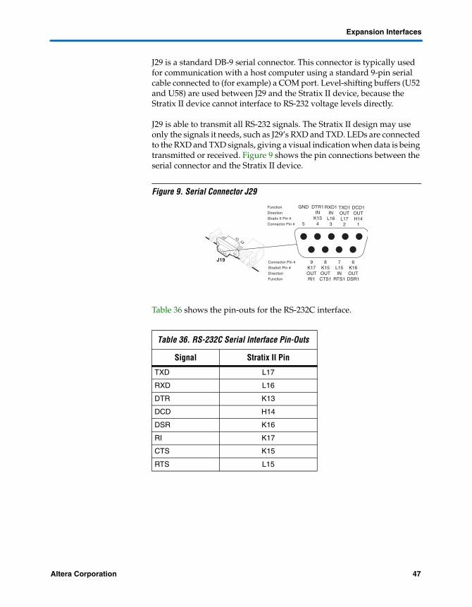
J29 is a standard DB-9 serial connector. This connector is typically used for communication with a host computer using a standard 9-pin serial cable connected to (for example) a COM port. Level-shifting buffers (U52 and U58) are used between J29 and the Stratix II device, because the Stratix II device cannot interface to RS-232 voltage levels directly.
J29 is able to transmit all RS-232 signals. The Stratix II design may use only the signals it needs, such as J29’s RXD and TXD. LEDs are connected to the RXD and TXD signals, giving a visual indication when data is being transmitted or received. Figure 9 shows the pin connections between the serial connector and the Stratix II device.
Figure 9. Serial Connector J29
Table 36 shows the pin-outs for the RS-232C interface.
Table 36. RS-232C Serial Interface Pin-Outs
Signal Stratix II Pin
TXD L17
RXD L16
DTR K13
DCD H14
DSR K16
RI K17
CTS K15
RTS L15
Function
Direction
Stratix II Pin #
Connector Pin #
Connector Pin #
StratixII Pin #
Direction
Function
GND
5
DTR1IN
K134
RXD1IN
L163
TXD1OUTL17
2
DCD1OUTH14
1
9K17OUTRI1
8K15OUTCTS1
7L15IN
RTS1
6K16OUTDSR1
J19
Altera Corporation 47Preliminary

Stratix II EP2S60 DSP Development Board Data Sheet
Table 37 lists reference information for the RS-232C transciever device.
Analog Devices Corporation External A/D Support
The Stratix II EP2S60 DSP development board supports Analog Devices A/D converters via two 40-pin 0.1-inch digital I/O headers (J5, J6). These two dual-purpose digital I/O headers can support a maximum of the following three converters.
■ Two AD9433 converters■ Two AD6645 converters■ One AD9430 converter
Table 38 lists the pin-outs for the ADI connectors.
Table 37. RS-232C Interface Device Reference
Item Description
Board reference U41
Part number MAX221E
Device description RS-232 transceiver
Voltage 3.3 V
Manufacturer Maxim
Manufacturer web site
www.maxim-ic.com
Table 38. ADI Connector (J5, J6) Pin-Outs (Part 1 of 2)
ADI Signal Name Stratix II Pin
Adi_D0 L3
Adi_D1 L4
Adi_D2 N4
Adi_D3 N5
Adi_D4 M3
Adi_D5 M4
Adi_D6 L1
Adi_D7 L2
Adi_D8 N2
Adi_D9 N3
Adi_D10 M1
48 Altera CorporationPreliminary

Expansion Interfaces
Adi_D11 M2
Adi_D12 R2
Adi_D13 R3
Adi_D14 P1
Adi_D15 P2
Adi_D16 J6
Adi_D17 J7
Adi_D18 J8
Adi_D19 J9
Adi_D20 K8
Adi_D21 K9
Adi_D22 L9
Adi_D23 L10
Adi_D24 L7
Adi_D25 L8
Adi_D26 K6
Adi_D27 K7
Adi_D28 L5
Adi_D29 L6
Adi_D30 M10
Adi_D31 M11
Adi_D32 M8
Adi_D33 M9
Table 38. ADI Connector (J5, J6) Pin-Outs (Part 2 of 2)
ADI Signal Name Stratix II Pin
Altera Corporation 49Preliminary
Stratix II EP2S60 DSP Development Board Data Sheet
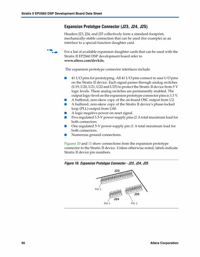
Expansion Prototype Connector (J23, J24, J25)
Headers J23, J24, and J25 collectively form a standard-footprint, mechanically-stable connection that can be used (for example) as an interface to a special-function daughter card.
f For a list of available expansion daughter cards that can be used with the Stratix II EP2S60 DSP development board refer to www.altera.com/devkits.
The expansion prototype connector interfaces include:
■ 41 I/O pins for prototyping. All 41 I/O pins connect to user I/O pins on the Stratix II device. Each signal passes through analog switches (U19, U20, U21, U22 and U25) to protect the Stratix II device from 5 V logic levels. These analog switches are permanently enabled. The output logic-level on the expansion prototype connector pins is 3.3 V.
■ A buffered, zero-skew copy of the on-board OSC output from U2.■ A buffered, zero-skew copy of the Stratix II device’s phase-locked
loop (PLL)-output from U60.■ A logic-negative power-on reset signal.■ Five regulated 3.3-V power-supply pins (2 A total maximum load for
both connectors.■ One regulated 5-V power-supply pin (1 A total maximum load for
both connectors.■ Numerous ground connections.
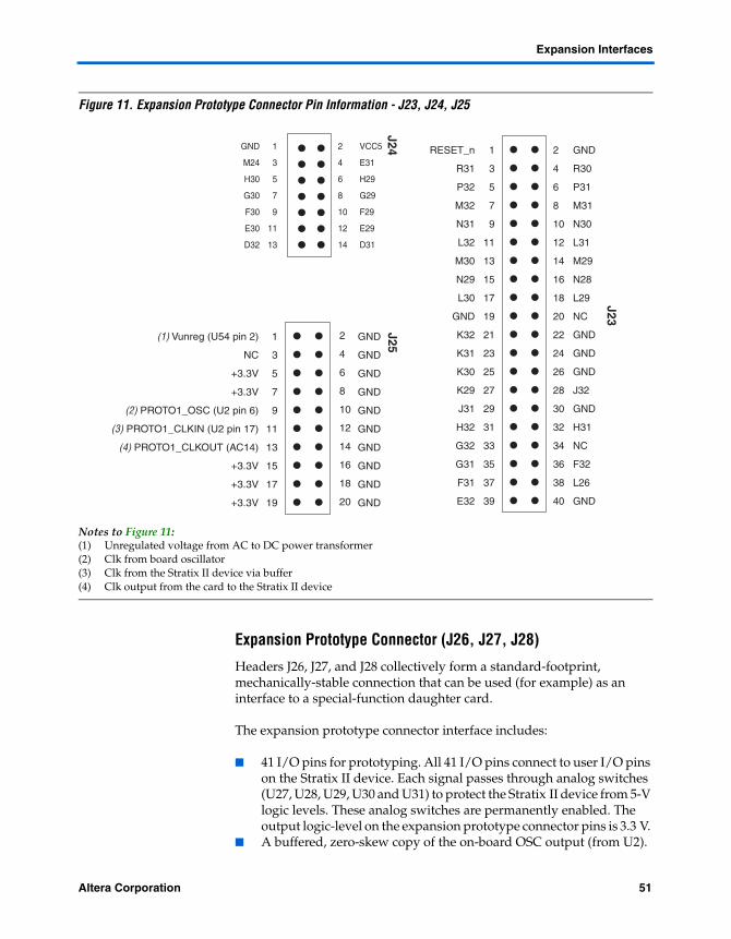
Figures 10 and 11 show connections from the expansion prototype connector to the Stratix II device. Unless otherwise noted, labels indicate Stratix II device pin numbers.
Figure 10. Expansion Prototype Connector - J23, J24, J25
Pin 1
J23
J24
J25
Pin 1
Pin 1
50 Altera CorporationPreliminary
Expansion Interfaces
Figure 11. Expansion Prototype Connector Pin Information - J23, J24, J25
Notes to Figure 11:(1) Unregulated voltage from AC to DC power transformer(2) Clk from board oscillator(3) Clk from the Stratix II device via buffer(4) Clk output from the card to the Stratix II device
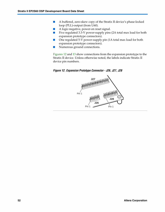
Expansion Prototype Connector (J26, J27, J28)
Headers J26, J27, and J28 collectively form a standard-footprint, mechanically-stable connection that can be used (for example) as an interface to a special-function daughter card.
The expansion prototype connector interface includes:
■ 41 I/O pins for prototyping. All 41 I/O pins connect to user I/O pins on the Stratix II device. Each signal passes through analog switches (U27, U28, U29, U30 and U31) to protect the Stratix II device from 5-V logic levels. These analog switches are permanently enabled. The output logic-level on the expansion prototype connector pins is 3.3 V.
■ A buffered, zero-skew copy of the on-board OSC output (from U2).
RESET_n
R31
P32
M32
N31
L32
M30
N29
L30
GND
K32
K31
K30
K29
J31
H32
G32
G31
F31
E32
GND
R30
P31
M31
N30
L31
M29
N28
L29
NC
GND
GND
GND
J32
GND
H31
NC
F32
L26
GND
1
3
5
7
9
11
13
15
17
19
21
23
25
27
29
31
33
35
37
39
2
4
6
8
10
12
14
16
18
20
22
24
26
28
30
32
34
36
38
40
J24
J23
(1) Vunreg (U54 pin 2)
NC
+3.3V
+3.3V
(2) PROTO1_OSC (U2 pin 6)
(3) PROTO1_CLKIN (U2 pin 17)
(4) PROTO1_CLKOUT (AC14)
+3.3V
+3.3V
+3.3V
GND
GND
GND
GND
GND
GND
GND
GND
GND
GND
1
3
5
7
9
11
13
15
17
19
2
4
6
8
10
12
14
16
18
20
GND
M24
H30
G30
F30
E30
D32
VCC5
E31
H29
G29
F29
E29
D31
1
3
5
7
9
11
13
2
4
6
8
10
12
14
J25
Altera Corporation 51Preliminary
Stratix II EP2S60 DSP Development Board Data Sheet
■ A buffered, zero-skew copy of the Stratix II device’s phase-locked loop (PLL)-output (from U60).
■ A logic-negative, power-on reset signal.■ Five regulated 3.3-V power-supply pins (2A total max load for both
expansion prototype connectors).■ One regulated 5-V power-supply pin (1A total max load for both
expansion prototype connectors).■ Numerous ground connections.
Figures 12 and 13 show connections from the expansion prototype to the Stratix II device. Unless otherwise noted, the labels indicate Stratix II device pin numbers.
Figure 12. Expansion Prototype Connector - J26, J27, J28
Pin 1
J26J28
J27
Pin 1
Pin 1
52 Altera CorporationPreliminary
Expansion Interfaces
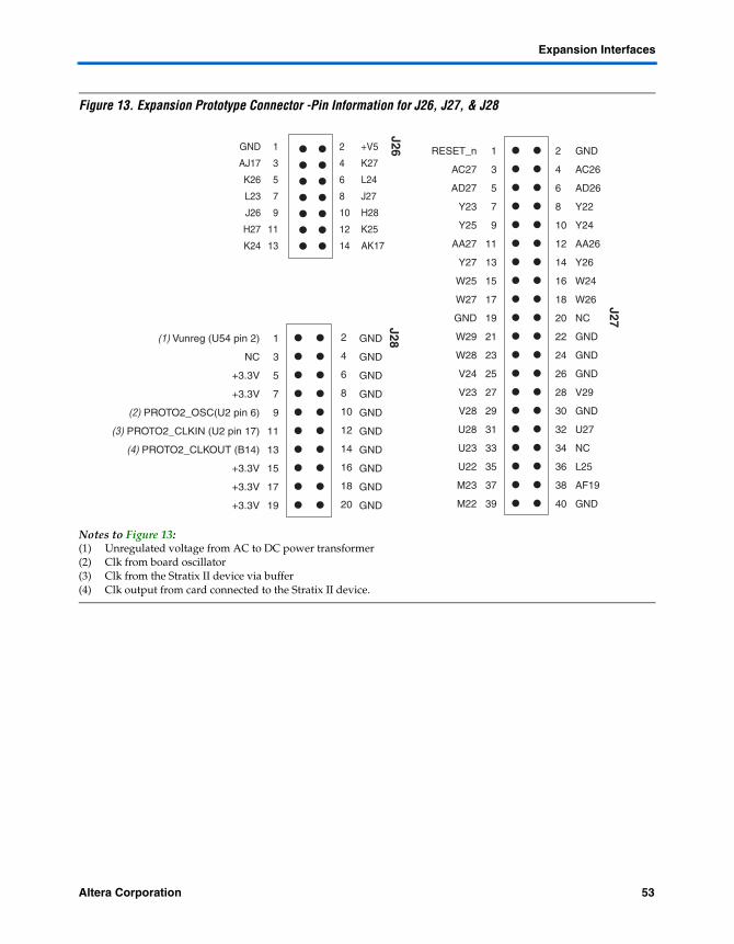
Figure 13. Expansion Prototype Connector -Pin Information for J26, J27, & J28
Notes to Figure 13:(1) Unregulated voltage from AC to DC power transformer(2) Clk from board oscillator(3) Clk from the Stratix II device via buffer(4) Clk output from card connected to the Stratix II device.
RESET_n
AC27
AD27
Y23
Y25
AA27
Y27
W25
W27
GND
W29
W28
V24
V23
V28
U28
U23
U22
M23
M22
GND
AC26
AD26
Y22
Y24
AA26
Y26
W24
W26
NC
GND
GND
GND
V29
GND
U27
NC
L25
AF19
GND
1
3
5
7
9
11
13
15
17
19
21
23
25
27
29
31
33
35
37
39
2
4
6
8
10
12
14
16
18
20
22
24
26
28
30
32
34
36
38
40
J26
J27
(1) Vunreg (U54 pin 2)
NC
+3.3V
+3.3V
(2) PROTO2_OSC(U2 pin 6)
(3) PROTO2_CLKIN (U2 pin 17)
(4) PROTO2_CLKOUT (B14)
+3.3V
+3.3V
+3.3V
GND
GND
GND
GND
GND
GND
GND
GND
GND
GND
1
3
5
7
9
11
13
15
17
19
2
4
6
8
10
12
14
16
18
20
GND
AJ17
K26
L23
J26
H27
K24
+V5
K27
L24
J27
H28
K25
AK17
1
3
5
7
9
11
13
2
4
6
8
10
12
14
J28
Altera Corporation 53Preliminary
Stratix II EP2S60 DSP Development Board Data Sheet
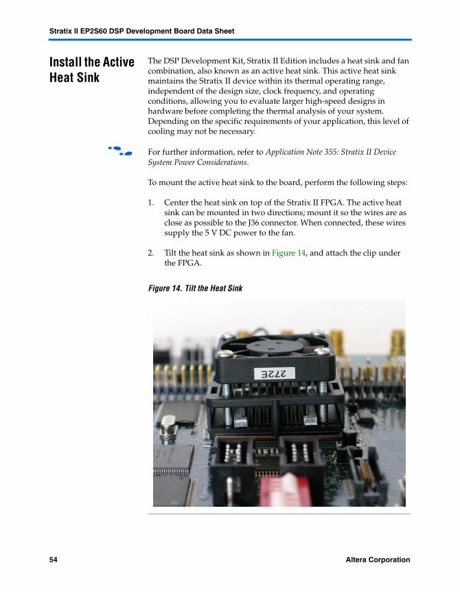
Install the Active Heat Sink
The DSP Development Kit, Stratix II Edition includes a heat sink and fan combination, also known as an active heat sink. This active heat sink maintains the Stratix II device within its thermal operating range, independent of the design size, clock frequency, and operating conditions, allowing you to evaluate larger high-speed designs in hardware before completing the thermal analysis of your system. Depending on the specific requirements of your application, this level of cooling may not be necessary.
f For further information, refer to Application Note 355: Stratix II Device System Power Considerations.
To mount the active heat sink to the board, perform the following steps:
1. Center the heat sink on top of the Stratix II FPGA. The active heat sink can be mounted in two directions; mount it so the wires are as close as possible to the J36 connector. When connected, these wires supply the 5 V DC power to the fan.
2. Tilt the heat sink as shown in Figure 14, and attach the clip under the FPGA.
Figure 14. Tilt the Heat Sink
54 Altera CorporationPreliminary
Expansion Interfaces
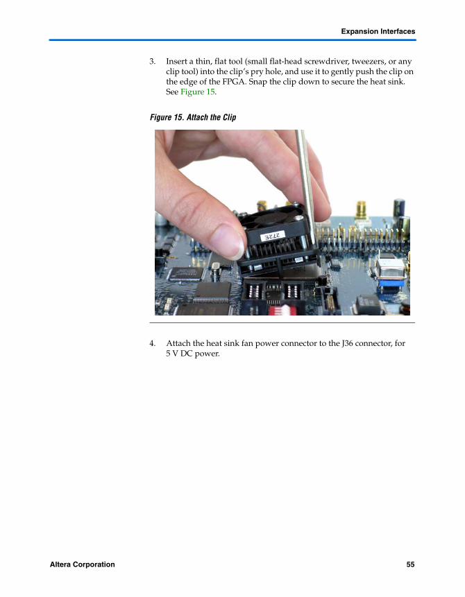
3. Insert a thin, flat tool (small flat-head screwdriver, tweezers, or any clip tool) into the clip’s pry hole, and use it to gently push the clip on the edge of the FPGA. Snap the clip down to secure the heat sink. See Figure 15.
Figure 15. Attach the Clip
4. Attach the heat sink fan power connector to the J36 connector, for 5 V DC power.
Altera Corporation 55Preliminary
Stratix II EP2S60 DSP Development Board
Remove the Active Heat Sink
To remove the heat sink and fan from the board, perform the following steps:
1. Disconnect the heat sink fan power connector from the J36 connector.
2. Insert the thin, flat tool into one of the clip’s pry holes. Using the tool, slightly push away and lift the plastic clip from the FPGA to detach one side of the heat sink.
3. Repeat step 2 on the other side of the plastic clip to remove the heat sink completely.
56 Altera CorporationPreliminary
101 Innovation DriveSan Jose, CA 95134(408) 544-7000www.altera.comApplications Hotline:(800) 800-EPLDLiterature Services:[email protected]
Copyright © 2005 Altera Corporation. All rights reserved. Altera, The Programmable Solutions Company,the stylized Altera logo, specific device designations, and all other words and logos that are identified astrademarks and/or service marks are, unless noted otherwise, the trademarks and service marks of AlteraCorporation in the U.S. and other countries. All other product or service names are the property of their re-spective holders. Altera products are protected under numerous U.S. and foreign patents and pendingapplications, maskwork rights, and copyrights. Altera warrants performance of its semiconductor productsto current specifications in accordance with Altera's standard warranty, but reserves the right to make chang-es to any products and services at any time without notice. Altera assumes no responsibility or liabilityarising out of the application or use of any information, product, or service describedherein except as expressly agreed to in writing by Altera Corporation. Altera customersare advised to obtain the latest version of device specifications before relying on any pub-lished information and before placing orders for products or services.