Embed Size (px)
Citation preview
Jim Koonmen, SVP ASML
Silicon Valley Lunch Forum, 25 April 2013
Stronger partnerships:
Reducing risks, accelerating progress
Agenda
• Partnerships 2.0 – Accelerate and de-risk new technologies
• EUV – Progress and update
• Immersion – Double patterning update
• 450 mm update
• Summary and conclusions
25 April 2013
Public
Slide 2
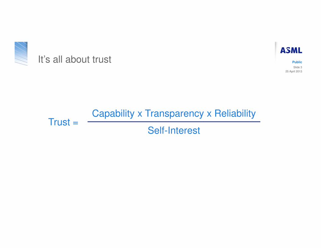
It’s all about trust
Trust = Capability x Transparency x Reliability
Self-Interest
25 April 2013
Public
Slide 3
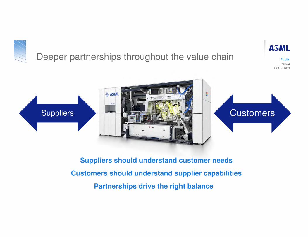
Suppliers Customers
Deeper partnerships throughout the value chain
Suppliers should understand customer needs
Partnerships drive the right balance
Customers should understand supplier capabilities
25 April 2013
Public
Slide 4
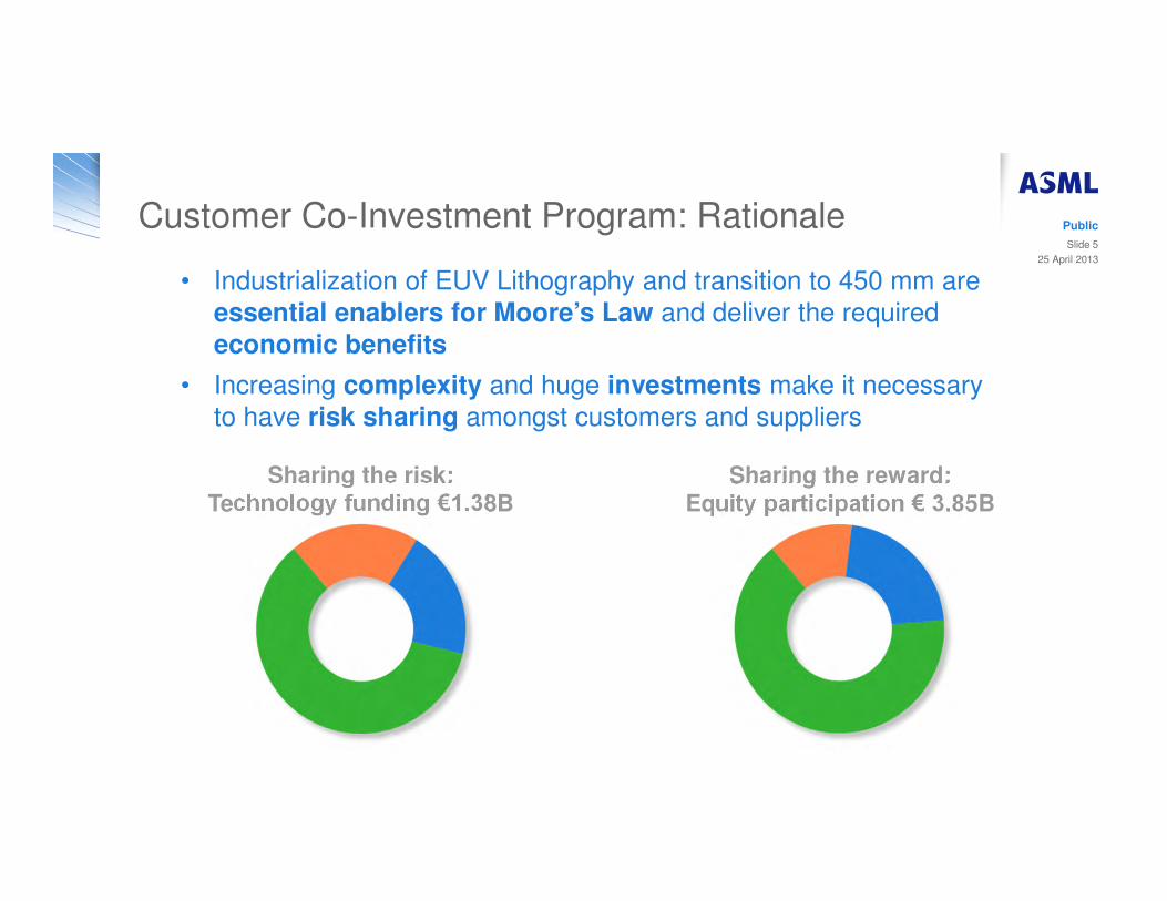
Customer Co-Investment Program: Rationale
• Industrialization of EUV Lithography and transition to 450 mm are
essential enablers for Moore’s Law and deliver the required
economic benefits
• Increasing complexity and huge investments make it necessary
to have risk sharing amongst customers and suppliers
Sharing the reward:Equity participation € 3.85B
Sharing the risk:Technology funding €1.38B
25 April 2013
Public
Slide 5
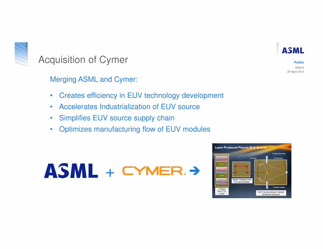
Acquisition of Cymer
Merging ASML and Cymer:
• Creates efficiency in EUV technology development
• Accelerates Industrialization of EUV source
• Simplifies EUV source supply chain
• Optimizes manufacturing flow of EUV modules
+ �
25 April 2013
Public
Slide 6
Agenda
• Partnerships 2.0 – Accelerate and de-risk new technologies
• EUV – Progress and update
• Immersion – Double patterning update
• 450 mm update
• Summary and conclusions
25 April 2013
Public
Slide 7
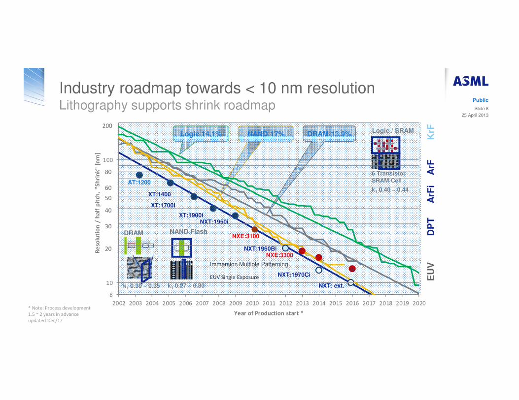
Industry roadmap towards < 10 nm resolution Lithography supports shrink roadmap
ArF
ArF
iE
UV
KrF
DP
T
Logic / SRAM
6 Transistor SRAM Cell
k1 0.40 ~ 0.44
Logic 14.1% NAND 17% DRAM 13.9%
* Note: Process development
1.5 ~ 2 years in advance
updated Dec/12
200
k1 0.30 ~ 0.35
DRAM
k1 0.27 ~ 0.30
NAND Flash
XT:1400
XT:1700i
AT:1200
XT:1900i NXT:1950i
20
30
40
50
60
80
NXE:3100
NXE:3300
NXT:1970Ci
NXT:1960Bi
NXT: ext.10
100
Re
solu
tio
n /
ha
lf p
itch
, "
Sh
rin
k"
[n
m]
8
2002 2003 2004 2005 2006 2007 2008 2009 2010 2011 2012 2013 2014 2015 2016 2017 2018 2019 2020
Year of Production start *
Immersion Multiple Patterning
EUV Single Exposure
25 April 2013
Public
Slide 8
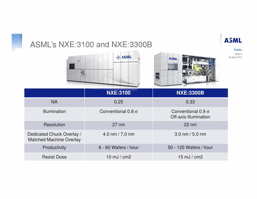
ASML’s NXE:3100 and NXE:3300B
NXE:3100 NXE:3300B
NA 0.25 0.33
Illumination Conventional 0.8 σ Conventional 0.9 σOff-axis illumination
Resolution 27 nm 22 nm
Dedicated Chuck Overlay / Matched Machine Overlay
4.0 nm / 7.0 nm 3.0 nm / 5.0 nm
Productivity 6 - 60 Wafers / hour 50 - 125 Wafers / hour
Resist Dose 10 mJ / cm2 15 mJ / cm2
25 April 2013
Public
Slide 9
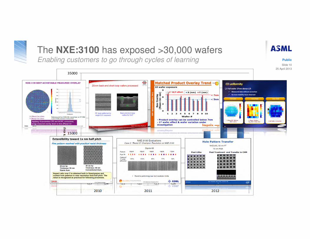
0
5000
10000
15000
20000
25000
30000
35000
Q3 Q4 Q1 Q2 Q3 Q4 Q1 Q2 Q3 Q4
2010 2011 2012
To
tal
wa
fers
ex
po
sed
on
NX
E:3
10
0
The NXE:3100 has exposed >30,000 wafersEnabling customers to go through cycles of learning
25 April 2013
Public
Slide 10
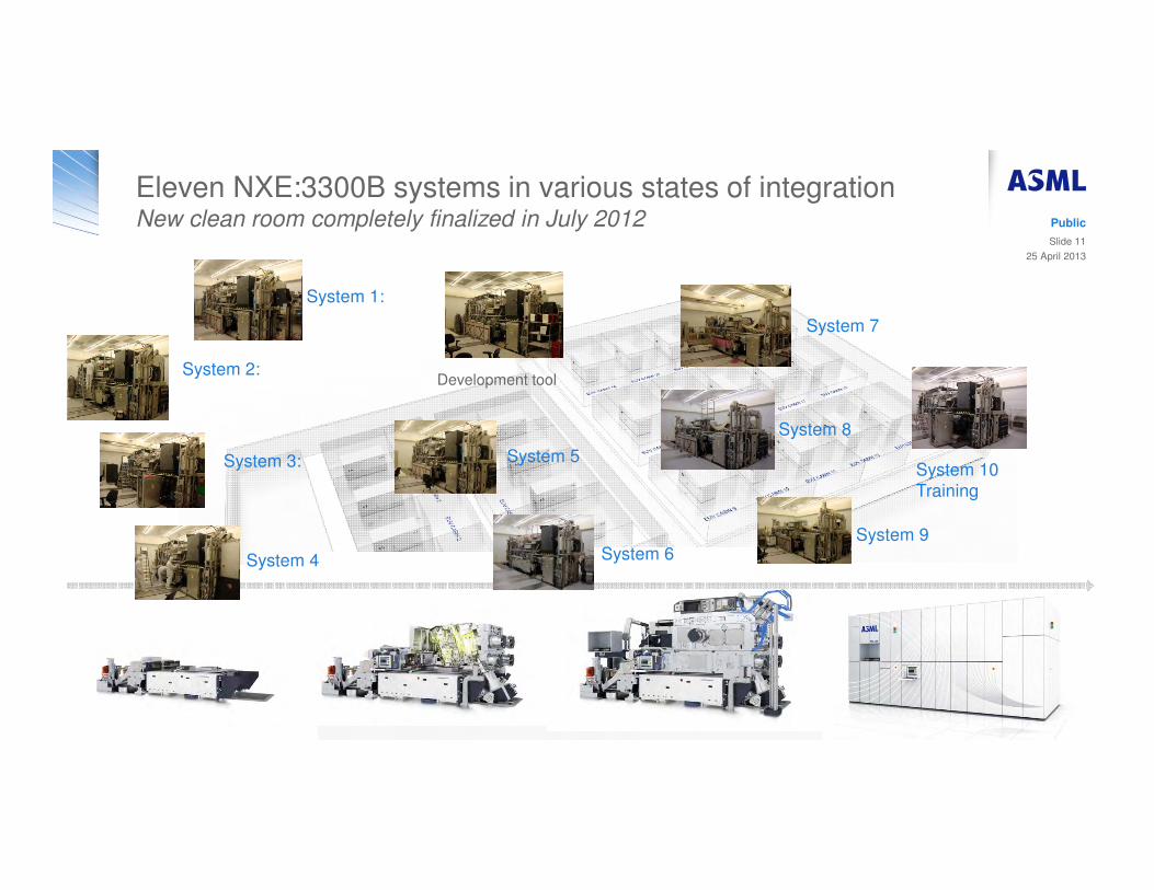
Eleven NXE:3300B systems in various states of integration New clean room completely finalized in July 2012
System 3:
System 1:
System 9
System 4
System 7
System 5
System 6
Development toolSystem 2:
System 8
System 10
Training
25 April 2013
Public
Slide 11
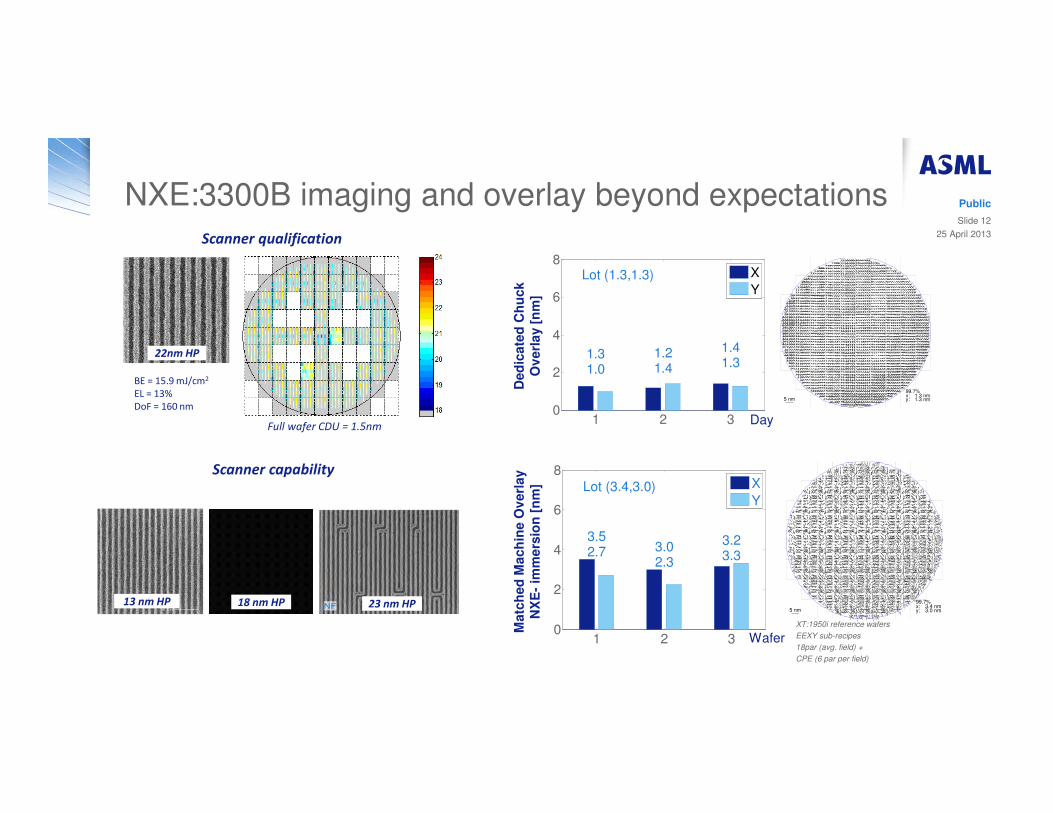
Ded
icate
d C
hu
ck
Ov
erl
ay [
nm
]
1 2 30
2
4
6
8Lot (1.3,1.3)
1.31.0
1.21.4
1.41.3
X
Y
Day
5 nm
99.7%x: 1.3 nmy: 1.3 nm
Filtered S2F Chuck 1 (S2F)
NXE:3300B imaging and overlay beyond expectations
Matc
hed
Mach
ine O
verl
ay
NX
E-
imm
ers
ion
[n
m]
1 2 30
2
4
6
8
Lot (3.4,3.0)
3.52.7 3.0
2.3
3.23.3
X
Y
Wafer
5 nm
99.7%x: 3.4 nmy: 3.0 nm
Filtered S2F (S2F)
XT:1950i reference wafers
EEXY sub-recipes
18par (avg. field) +
CPE (6 par per field)
Full wafer CDU = 1.5nm
22nm HP
BE = 15.9 mJ/cm2
EL = 13%
DoF = 160 nm
Scanner qualification
Scanner capability
18 nm HP13 nm HP 23 nm HP
25 April 2013
Public
Slide 12
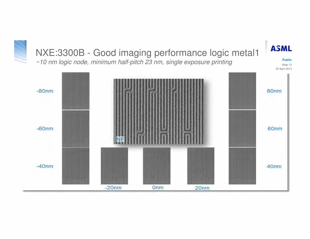
NXE:3300B - Good imaging performance logic metal1 ~10 nm logic node, minimum half-pitch 23 nm, single exposure printing
25 April 2013
Public
Slide 13
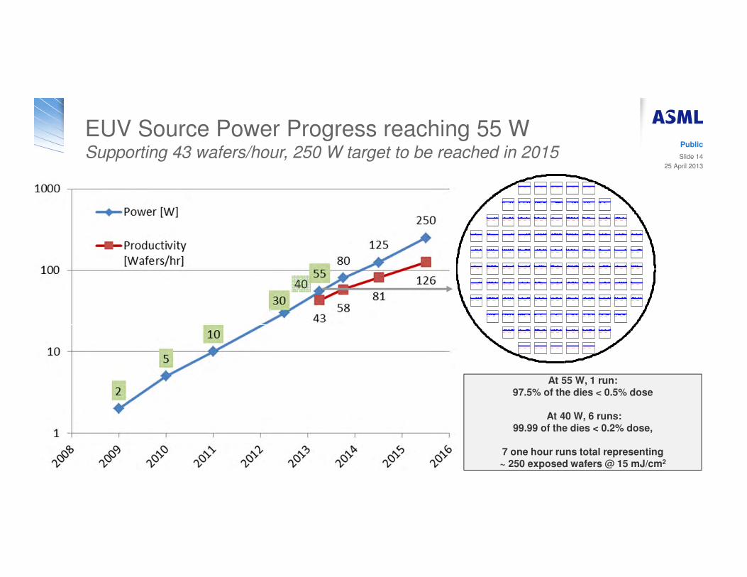
EUV Source Power Progress reaching 55 WSupporting 43 wafers/hour, 250 W target to be reached in 2015
At 55 W, 1 run: 97.5% of the dies < 0.5% dose
At 40 W, 6 runs: 99.99 of the dies < 0.2% dose,
7 one hour runs total representing ~ 250 exposed wafers @ 15 mJ/cm2
40
25 April 2013
Public
Slide 14
Agenda
• Partnerships 2.0 – Accelerate and de-risk new technologies
• EUV – Progress and update
• Immersion – Double patterning update
• 450 mm update
• Summary and conclusions
25 April 2013
Public
Slide 15
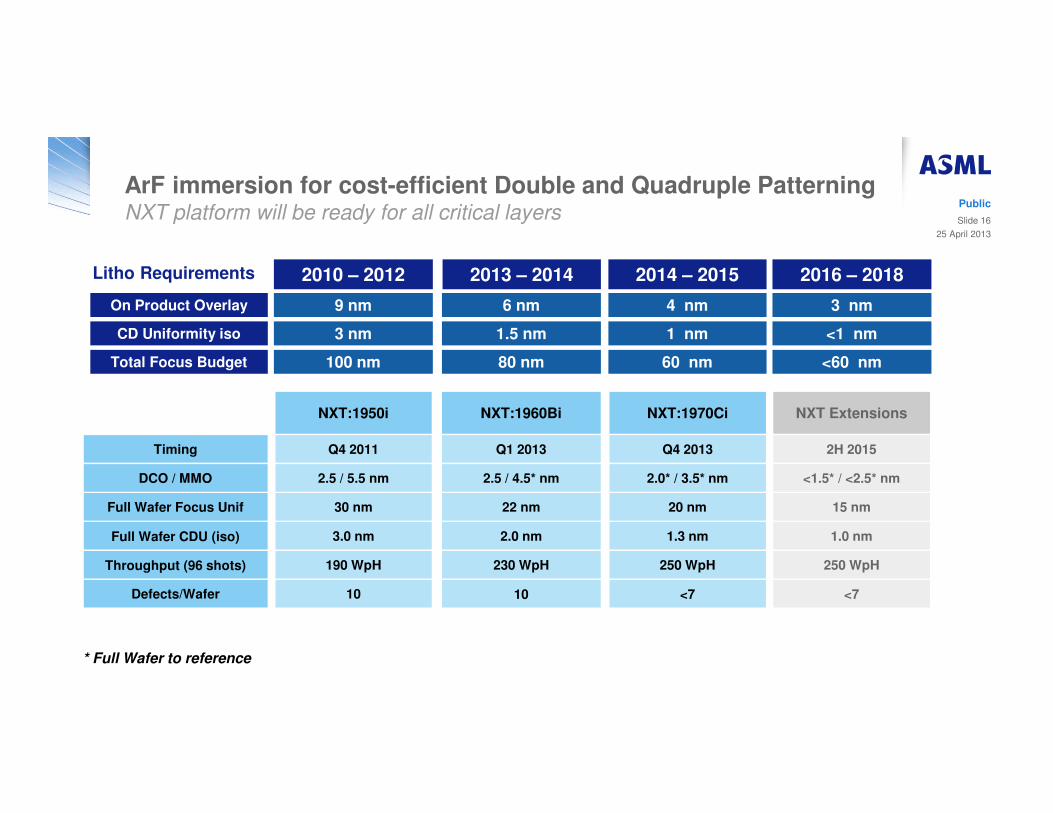
ArF immersion for cost-efficient Double and Quadruple PatterningNXT platform will be ready for all critical layers
NXT:1950i NXT:1960Bi NXT:1970Ci NXT Extensions
Timing Q4 2011 Q1 2013 Q4 2013 2H 2015
DCO / MMO 2.5 / 5.5 nm 2.5 / 4.5* nm 2.0* / 3.5* nm <1.5* / <2.5* nm
Full Wafer Focus Unif 30 nm 22 nm 20 nm 15 nm
Full Wafer CDU (iso) 3.0 nm 2.0 nm 1.3 nm 1.0 nm
Throughput (96 shots) 190 WpH 230 WpH 250 WpH 250 WpH
Defects/Wafer 10 10 <7 <7
9 nmOn Product Overlay 6 nm 4 nm
3 nmCD Uniformity iso 1.5 nm 1 nm
100 nmTotal Focus Budget 80 nm 60 nm
2010 – 2012 2013 – 2014 2014 – 2015Litho Requirements
3 nm
<1 nm
<60 nm
2016 – 2018
* Full Wafer to reference
25 April 2013
Public
Slide 16
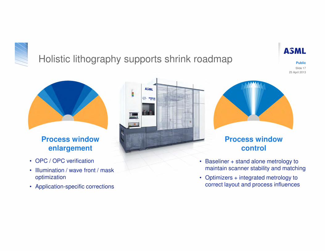
Holistic lithography supports shrink roadmap
Process window enlargement
Process window control
• OPC / OPC verification
• Illumination / wave front / mask optimization
• Application-specific corrections
• Baseliner + stand alone metrology to maintain scanner stability and matching
• Optimizers + integrated metrology to correct layout and process influences
25 April 2013
Public
Slide 17
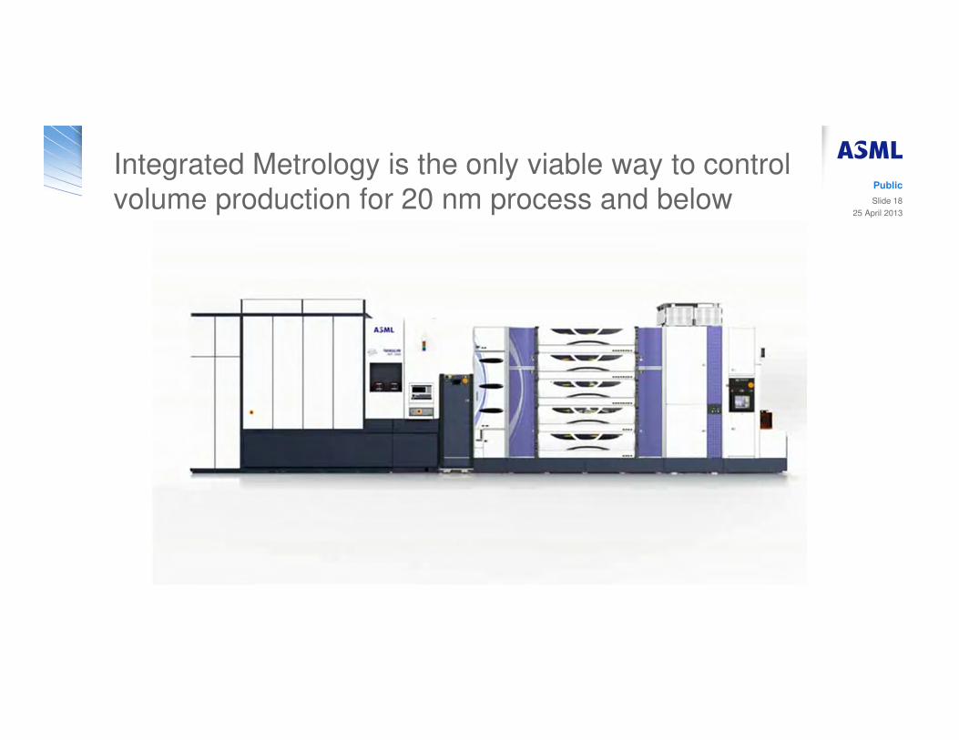
Integrated Metrology is the only viable way to control
volume production for 20 nm process and below25 April 2013
Public
Slide 18
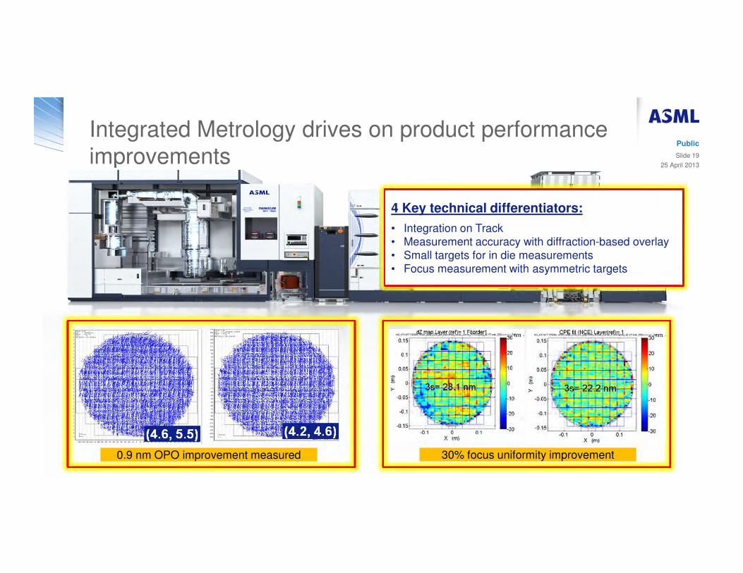
Integrated Metrology drives on product performance
improvements
(4.6, 5.5) (4.2, 4.6)
0.9 nm OPO improvement measured 30% focus uniformity improvement
4 Key technical differentiators:
• Integration on Track
• Measurement accuracy with diffraction-based overlay
• Small targets for in die measurements
• Focus measurement with asymmetric targets
25 April 2013
Public
Slide 19
Agenda
• Partnerships 2.0 – Accelerate and de-risk new technologies
• EUV – Progress and update
• Immersion – Double patterning update
• 450 mm update
• Summary and conclusions
25 April 2013
Public
Slide 20
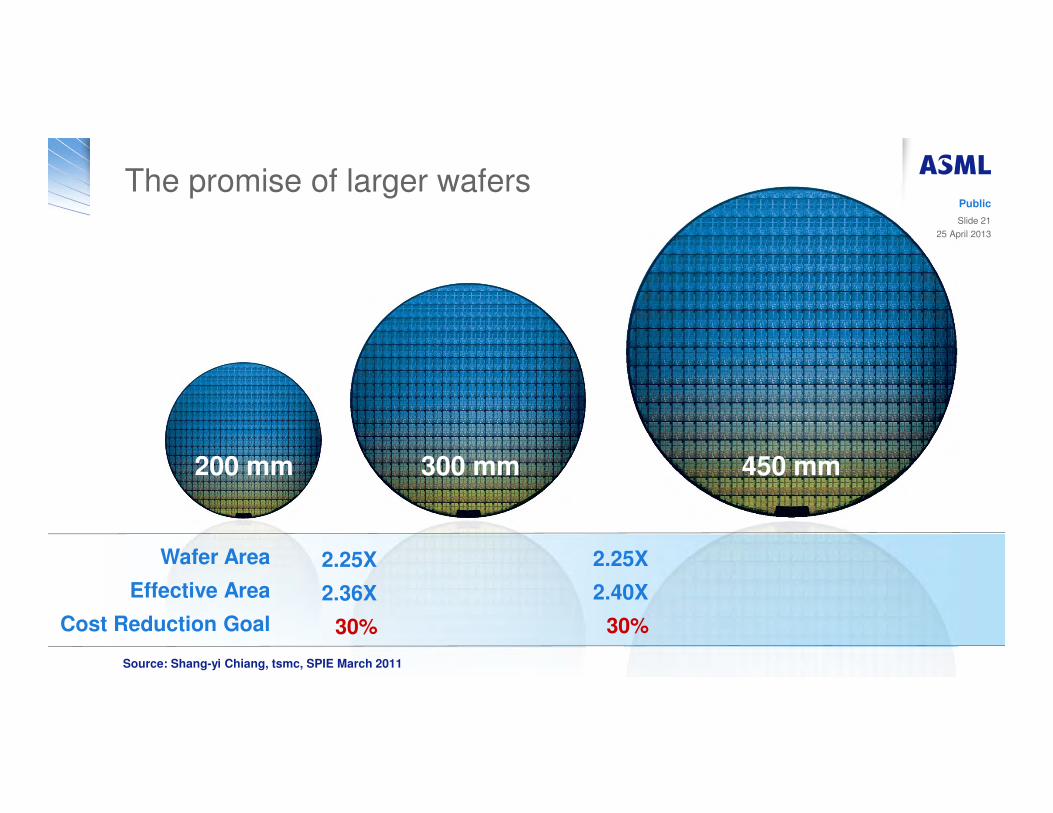
The promise of larger wafers
Source: Shang-yi Chiang, tsmc, SPIE March 2011
200 mm 300 mm 450 mm
Wafer Area
Effective Area
Cost Reduction Goal
2.25X
2.36X
30%
2.25X
2.40X
30%
25 April 2013
Public
Slide 21
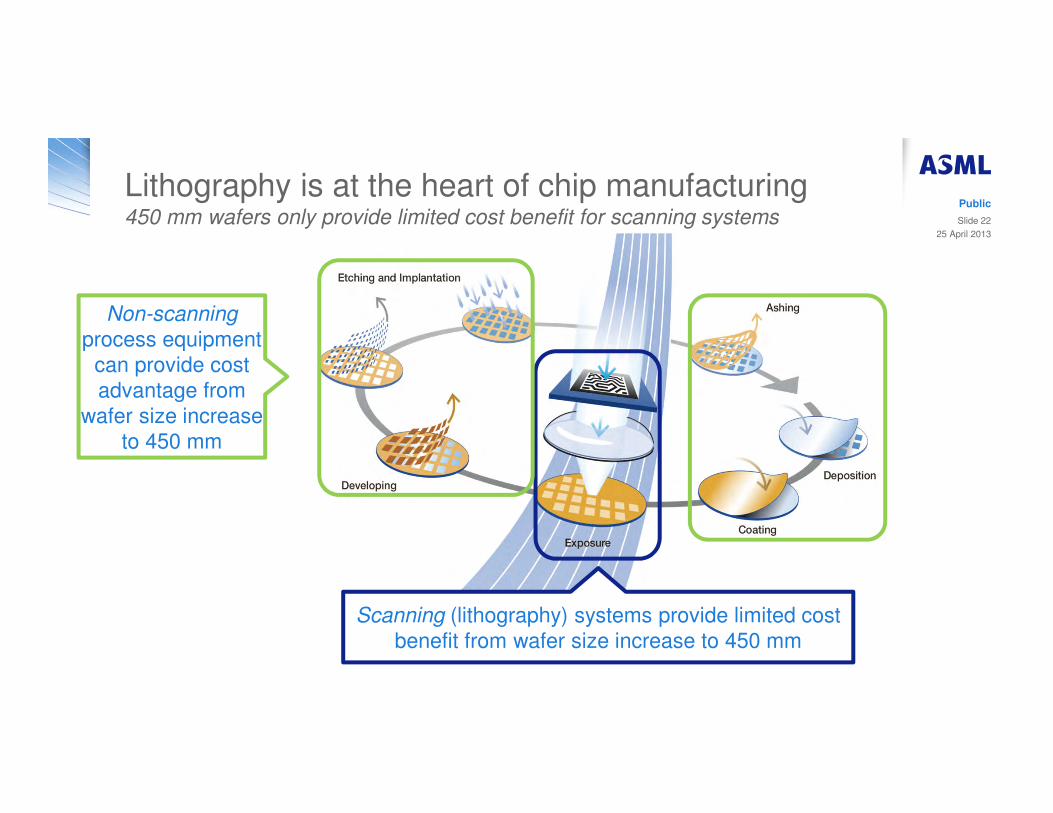
Non-scanning
process equipment
can provide cost
advantage from
wafer size increase
to 450 mm
Lithography is at the heart of chip manufacturing450 mm wafers only provide limited cost benefit for scanning systems
Scanning (lithography) systems provide limited cost
benefit from wafer size increase to 450 mm
25 April 2013
Public
Slide 22
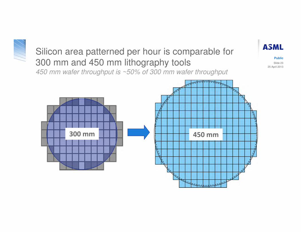
450 mm300 mm
Silicon area patterned per hour is comparable for
300 mm and 450 mm lithography tools450 mm wafer throughput is ~50% of 300 mm wafer throughput
25 April 2013
Public
Slide 23
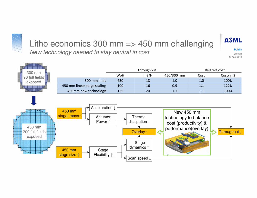
450 mm
stage mass↑
Acceleration ↓
Throughput ↓
Actuator
Power ↑
Thermal
dissipation ↑
Overlay↑
450 mm
stage size ↑
Stage
Flexibility ↑
Stage
dynamics ↑
Scan speed ↓
Litho economics 300 mm => 450 mm challengingNew technology needed to stay neutral in cost
300 mm
96 full fields
exposed
450 mm
200 full fields
exposed
New 450 mm technology to balance cost (productivity) &
performance(overlay)
throughput Relative cost
WpH m2/H 450/300 mm Cost Cost/ m2
300 mm limit 250 18 1.0 1.0 100%
450 mm linear stage scaling 100 16 0.9 1.1 122%
450mm new technology 125 20 1.1 1.1 100%
25 April 2013
Public
Slide 24
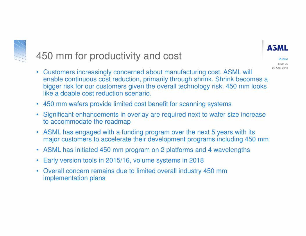
450 mm for productivity and cost
• Customers increasingly concerned about manufacturing cost. ASML will enable continuous cost reduction, primarily through shrink. Shrink becomes a bigger risk for our customers given the overall technology risk. 450 mm looks like a doable cost reduction scenario.
• 450 mm wafers provide limited cost benefit for scanning systems
• Significant enhancements in overlay are required next to wafer size increase to accommodate the roadmap
• ASML has engaged with a funding program over the next 5 years with its major customers to accelerate their development programs including 450 mm
• ASML has initiated 450 mm program on 2 platforms and 4 wavelengths
• Early version tools in 2015/16, volume systems in 2018
• Overall concern remains due to limited overall industry 450 mm implementation plans
25 April 2013
Public
Slide 25
Agenda
• Partnerships 2.0 – Accelerate and de-risk new technologies
• EUV – Progress and update
• Immersion – Double patterning update
• 450 mm update
• Summary and conclusions
25 April 2013
Public
Slide 26
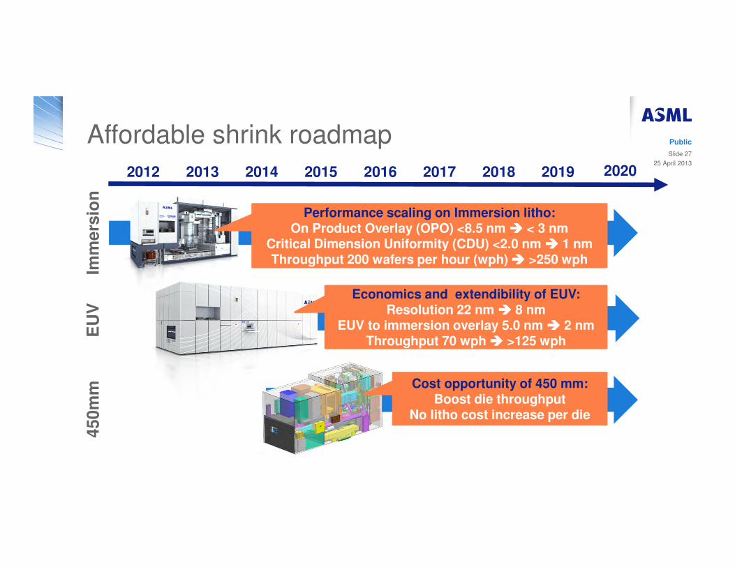
Affordable shrink roadmap
NXE:3300B, NXE:3350, …
NXT:1950i, NXT:1960Bi, NXT:1970Ci
2012 2013 2014 2015 2016 2017 2018 2019 2020
QXT, QXE
450m
mE
UV
Imm
ers
ion
Economics and extendibility of EUV:Resolution 22 nm ���� 8 nm
EUV to immersion overlay 5.0 nm ���� 2 nmThroughput 70 wph ���� >125 wph
Cost opportunity of 450 mm: Boost die throughput
No litho cost increase per die
Performance scaling on Immersion litho:On Product Overlay (OPO) <8.5 nm ���� < 3 nm
Critical Dimension Uniformity (CDU) <2.0 nm ���� 1 nmThroughput 200 wafers per hour (wph) ���� >250 wph
25 April 2013
Public
Slide 27
Summary and Conclusions
• In combination with a holistic approach, immersion technology is capable of supporting shrink to 14 & 10 nm:
• Optimization of mask, illuminator (FlexRay) and pupil (FlexWave)
• Integrated Metrology with Yieldstar
• Once power is sufficient for 125 wafers per hour, EUV becomes technology of choice for high volume production of key layers
• Key resources and stake holders aligned through co-investment program and Cymer acquisition
• Industry aligning on 450 mm insertion point around 10 nm node
• “EUV first, 450 mm later”
• More / deeper partnerships required throughout the industry to maintain speed and affordability
25 April 2013
Public
Slide 28