Embed Size (px)
Citation preview
STRUCTURE AND OPTICAL PROPERTIES OF MULTI-PHASE STRUCTURED AMORPHOUS
SILICON CARBON NITRIDE THIN FILMS DEPOSITED BY PLASMA ENHANCED CHEMICAL VAPOUR
DEPOSITION
MOHD AZAM BIN ABDUL RAHMAN
DEPARTMENT OF PHYSICS
FACULTY OF SCIENCE UNIVERSITY OF MALAYA
KUALA LUMPUR
2018
ii
ORIGINAL LITERARY WORK DECLARATION
Name of Candidate: MOHD AZAM BIN ABDUL RAHMAN (I.C/Passport No: 610805035023)
Registration/Matric No: SHC090067 Name of Degree: DOCTOR OF PHILOSOPHY Title of Project Paper/Research Report/Dissertation/Thesis (“this Work”): STRUCTURE AND OPTICAL PROPERTIES OF MULTI-PHASE STRUCTURED AMORPHOUS SILICON CARBON NITRIDE THIN FILMS DEPOSITED BY PLASMA ENHANCED CHEMICAL VAPOUR DEPOSITION Field of Study: EXPERIMENTAL PHYSICS I do solemnly and sincerely declare that: I am the sole author/writer of this Work; (1) This Work is original; (2) Any use of any work in which copyright exists was done by way of fair dealing and
for permitted purposes and any excerpt or extract from, or reference to or reproduction of any copyright work has been disclosed expressly and sufficiently and the title of the Work and its authorship have been acknowledged in this Work;
(3) I do not have any actual knowledge nor do I ought reasonably to know that the making of this work constitutes an infringement of any copyright work;
(4) I hereby assign all and every rights in the copyright to this Work to the University of Malaya (“UM”), who henceforth shall be owner of the copyright in this Work and that any reproduction or use in any form or by any means whatsoever is prohibited without the written consent of UM having been first had and obtained;
(5) I am fully aware that if in the course of making this Work I have infringed any copyright whether intentionally or otherwise, I may be subject to legal action or any other action as may be determined by UM.
Candidate’s Signature: Date: Subscribed and solemnly declared before, Witness’s Signature: Date: Name: DR. CHIU WEE SIONG Designation: SENIOR LECTURER
iii
STRUCTURE AND OPTICAL PROPERTIES OF MULTI-PHASE STRUCTURED AMORPHOUS SILICON CARBON NITRIDE THIN FILMS
DEPOSITED BY PLASMA ENHANCED CHEMICAL VAPOUR DEPOSITION
ABSTRACT
The amorphous structured silicon carbide (a-SiC) thin films have been the focus of many
studies due to its potential applications for high temperature devices operation in
complement to conventional silicon microelectronics. Incorporation of nitrogen to silicon
carbide thin films, has offered an effective route to produce hydrogenated amorphous
silicon carbon nitride (a-SiCN:H) that combines the properties of silicon carbide, silicon
nitride and carbon nitride. In current study, the variation in the structure, composition and
optical properties of multi-phase structured hydrogenated amorphous silicon carbide (a-
SiC:H) and a-SiCN:H thin films deposited by plasma-enhanced chemical vapour
deposition (PECVD) with respect to nitrogen flow-rate is the focus in the first part of this
work. Thereafter, the structure and optical properties of both multi-phase structured a-
SiC:H deposited from the discharge of silane and methane as well as a-SiCN:H thin films
deposited from the discharge of silane, methane and nitrogen with different flow-rate have
been investigated in detail by using spectroscopy techniques. With respect to this, FTIR
was used to probe the bonding structure in the film while Raman spectra of the films were
used to understand the microstructure properties of the films related to the C-C bonds.
Meanwhile, depth profiling analysis using Auger electron spectroscopy was used to probe
the elemental composition of the films. Optical transmittance and reflectance spectra were
utilized to determine the dispersion plot of refractive index of the films in the ultra-violet
to the near infrared region. The optical energy gaps of the films were determined from
the Tauc plot derived from the dispersion of absorption coefficient of the films calculated
from the optical transmission spectra of the films. Optical constants, dispersion energy
(ED) and single oscillator energy (E0) were determined from the dispersion of the
iv
refractive index plots using the Wemple-DiDomenico Model. The photoluminescence
properties of the films were investigated and the origin of photoluminescence were
accredited to the recombination within the tail states the hydrogenated amorphous carbon
(a-C:H) phase in the films structure where the tail states are formed from sp2-C clusters
in the film. The broad PL emission spectra were due to the overlapping of all the PL
emission produced by the different phases in the film structure. Finally, comparative
analysis was done on the structure and optical properties of the a-SiCN:H films after 30
days of deposition. Significant changes were observed in the chemical bonding properties
of the films and the changes were different for the films deposited with and without
nitrogen. The annealing of films at temperatures of 100 to 400 °C produced different
effects on the structure and optical properties of the a-SiC:H and a-SiCN:H films.
Decrease in the band gap energy value for the a-SiC:H film was due to evolution of
hydrogen atoms from Si-CH3 bonds and breaking of weak Si-C bonds. However, the
decrease in the band gap of the a-SiCN:H films was attributed to the decrease in C-N and
Si-C-N bonds content in the film structure.
Keywords: thin films, a-SiCN:H, PECVD.
v
SIFAT STRUKTUR DAN OPTIK FILEM NIPIS PELBAGAI FASA ARMOFUS SILIKON KARBON NITRIDA DIDEPOSITKAN DENGAN DEPOSISI VAPOR
KIMIA DIPERTINGKATKAN OLEH PLASMA
ABSTRAK
Filem nipis silicon karbida berstruktur amorfus (a-SiC) telah menjadi tumpuan kepada
banyak kajian kerana keupayaannya untuk digunakan sebagai pengoperasian peranti suhu
tinggi yang mampu menjadi pelengkap kepada mikroelektronik silikon konvensional.
Penglibatan nitrogen kepada filem nipis silikon karbida, telah menawarkan laluan yang
efektif untuk menghasilkan silikon karbon nitrida berhidrogen (a-SiCN: H) yang
menggabungkan sifat-sifat silikon karbida, silikon nitrida dan karbon nitrida. Dalam
kajian ini, variasi dalam struktur, komposisi dan sifat optik silikon karbida amorfus
berhidrogen (a-SiC:H) dan a-SiCN:H berstruktur multi-fasa yang dimendapkan dengan
kaedah pemendapan wap kimia secara peningkatan plasma (PECVD) merujuk kepada
kadar aliran nitrogen diberi tumpuan dalam bahagian pertama penyelidikan ini.
Selanjutnya, ciri-ciri struktur dan sifat optik kedua-dua filem nipis iaitu a-SiC:H
berstruktur multi-fasa yang dimendapkan daripada nyahcas silana dan metana dan a-
SiCN:H yang dimendapkan daripada nyahcas silana, metana dan nitrogen dengan kadar
aliran yang berbeza telah diselidiki secara terperinci dengan menggunakan teknik-teknik
spektroskopi. Sementara itu, analisa profil pendalaman oleh spektroskopi elektron Auger
digunakan untuk menyiasat komposisi elemen yang terdapat di dalam filem. Spektra
pemancaran dan pantulan optik digunakan untuk memperolehi plot sebaran indeks
pantulan dalam julat sinar ultra lembayung- inframerah hampir. Jurang tenaga optik filem
ditentukan dari plot Tauc yang diperolehi daripada penyebaran pekali penyerapan filem-
filem yang dikira dari spektrum penghantaran optik filem. Pemalar optik, tenaga
penyebaran (ED) dan tenaga pengayun tunggal (E0) ditentukan dari penyebaran plot
indeks biasan menggunakan Model Wemple-DiDomenico. Sifat kefotopendarcahayaan
vi
(PL) filem-filem ini telah diselidiki dan asalan kefotopendarcahayaan telah diakreditasi
kepada penggabungan semula di keadaan jalur ekor fasa karbon amorfus berhidrogen (a-
C:H) di dalam struktur filem di mana keadaan ekor terbentuk daripada kelompok sp2-C
di dalam filem. Spektrum pancaran PL yang lebar adalah disebabkan oleh pertidihan
kesemua pancaran PL yang dihasilkan oleh fasa-fasa yang berbeza di dalam struktur
filem. Akhir sekali, analisis perbandingan dilakukan pada struktur dan sifat optik filem a-SiCN:H
30 hari selepas pemendapan. Perubahan besar dapat dilihat terhadap ciri-ciri ikatan kimia filem
nipis dan perubahan bagi filem nipis termendap oleh nitrogen dan tanpa nitrogen adalah berbeza.
Pemanasan filem-filem a-SiC:H dan a-SiCN:H. dalam julat suhu 100 ke 400 °C memberikan
kesan berbeza kepada struktur dan sifat optik filem-filem. Penurunan nilai jurang jalur tenaga
bagi a-SiC:H adalah disebabkan oleh pembebasan atom hidrogen daripada ikatan Si-CH3
dan kemusnahan ikatan Si-C yang lemah. Namun demikian, penurunan dalam jurang
tenaga bagi a-SiCN:H adalah disebabkan oleh penurunan kandungan ikatan C-N dan Si-
C-N di dalam struktur filem.
Kata kunci: filem nipis, a-SiCN:H, PECVD
vii
ACKNOWLEDGEMENTS
I am grateful to the following peoples for their continuous supports throughout
current study. Without their assistance, current study would not be made possible.
Firstly, I would like to thank my supervisor (Prof. Datin Dr. Saadah Abdul
Rahman and Dr. Chiu Wee Siong) for their patience and brilliant ideas. Their prompt
actions in response to my difficulties and thesis planning are greatly appreciated.
Secondary, deepest gratitude to my co-supervisor (Prof. Mohamad Rusop from UiTM),
who have provided continuous supports in using facilities in his laboratories.
Thirdly, I would like to acknowledge Head of Physics Department (UM) for
providing well-equipped working environment. Special thanks to all staffs in Physics
Department and Faculty of Science for the analytical helps and administration task.
Furthermore, I would like to thank academic administrators from UiTM Dengkil
(Associate Professor Mohd Kamil, Mr. Mohd Isa and Nurhairulnizam bin Darus), who
had greatly assisted me by providing me flexibility to complete this thesis.
Also, I would like to acknowledge Dr. Goh Boon Tong, Ragib Badaruddin, Dr.
Fatemeh Shariatmadar Tehrani, Dr. Haw Choon Yian, Mr. Mohamad Aruf, Hamizah
Abdul Khanis, Chia Mei Yuen, Mohd Arif Sarjidan and all the members of Low
Dimensional Material Research Centre. All of them have provided very important
coordination to me in sharing information and technical skills.
Additionally, special thanks to UiTM for Bumiputera Academic Training Scheme
(SLAB/SLAI) to fund current enrolment. Also, financial supports from KPT under grant
FRGS (FP011/2015A) are highly acknowledged. Finally, special thanks to my wife
Azmawani Mohd Din @ Adam, my lovely children (Syahril Khalis, Nureen Syahirah,
Nessa Zahira and Dahlia Imani), who have tolerated my attention and occupancy during
the course of Phd life.
viii
TABLE OF CONTENTS
ABSTRACT ……………………………………………………………………...
ABSTRAK ………………………………………………………………………..
ACKNOWLEDGEMENT ………………………………………………………
TABLE OF CONTENTS ………………………………………………………..
LIST OF FIGURES ……………………………………………………………...
LIST OF TABLES ……………………………………………………………….
LIST OF ABBREVIATIONS ………………….………………………………..
iii
v
vii
viii
xiii
xviii
xix
CHAPTER 1: INTRODUCTION ………………………………………………..
1.1 History of Research on Silicon Carbon Nitride Thin Films ………………….
1.2 Importance of Silicon Carbon Nitride …………………………………..........
1.3 Research Problems and Motivation …………………………………………..
1.4 Research Objectives ………………………………………………………….
1.5 Organization of Thesis ……………………………………………………….
CHAPTER 2: BACKGROUND STUDIES LITERATURE REVIEW ………..
2.1 Introduction ……………………………………………………………..........
2.2 Silicon based Thin Films Technology: Strengths and Weaknesses ………….
2.3 Progress in Silicon- and Carbon-based Thin Films Alloys ……………..........
2.3.1 Silicon Carbide …….…………………………………………………..
2.3.2 Silicon Nitride ………………………………………………….............
2.3.3 Amorphous Carbon …………………………………………….............
2.3.4 Silicon Carbon Nitride …………………………………………………
2.4 Structural and Optical Properties of SiCN ……………………………………
2.4.1 Composition of a-SiCN ………………………………………………..
1
1
1
2
4
5
7
7
7
9
9
12
13
14
19
19
ix
2.4.2 Chemical Bonding ……………………………………………………..
2.4.3 Microstructure of a-SiCN ………………………………………………
2.4.4 Optical Properties ……………………………………………………...
2.4.5 Photoluminescence …………………………………………….............
2.5 Reviews on the Deposition Technique of Silicon and Carbon Based Thin
Films ……………………………………………………………….….……..
2.5.1 Chemical Vapour Deposition ………………………………………….
2.5.2 Radio Frequency Plasma Enhanced Chemical Vapour Deposition ……
2.5.3 Microwave PECVD ……………………………………………………
2.5.4 Hot wire CVD ……………..…………………………………………...
2.6 Ageing (Ageing effects on Si and Carbon based Compound) ………….
2.7 Post Annealing …………………………………………………………
CHAPTER 3: METHODOLOGY ………………………………………………..
3.1 Introduction …………….…………………………………………………….
3.2 PECVD Deposition System ………………………………………..…………
3.2.1 Thin Film Deposition Procedures ……………………………………...
3.3 Film Thickness Measurement …………………...……………………………
3.4 Annealing Technique ……………………………...…………………………
3.5 Safety Concern ……………………………...…………………………..........
3.6 Characterisation and Analytical Technique ………..…………………………
3.6.1 Auger Electron Spectroscopy Measurement ….……………………….
3.6.2 Fourier Transform Infrared Spectroscopy ...….………………………..
3.6.3 Raman Spectroscopy ………………………...….……………………..
3.6.4 UV-Vis Spectroscopy ...……………………...….……………………..
3.6.5 Optical Constants Calculation ....………………………………............
20
23
24
26
27
27
28
34
35
37
38
40
40
40
45
48
48
49
51
51
53
54
57
59
x
3.6.6 Optical Absorption and Energy Gap ...…………………………………
3.6.7 Refractive Index Dispersion Analysis ..………………………………..
3.6.8 Photoluminescence (PL) Spectroscopy ..……..………………………..
CHAPTER 4: EFFECTS OF NITROGEN FLOW-RATE TOWARDS THE
STRUCTURE OF MULTIPHASE STRUCTURED AMORPHOUS SILICON
CARBON NITRIDE THIN FILMS ………………………………………………
4.1 Introduction ……………………………………………………………..........
4.2 Effects of Nitrogen Gas Flow-Rate on the Elemental Composition of Multi-
Phase Structured Hydrogenated Amorphous Silicon Carbon Nitride Thin
Films: Auger Electron Spectroscopy ……………………...............................
4.3 Effects of Nitrogen Gas Flow-Rate on the Bonding Properties of Multi-Phase
Structured Hydrogenated Amorphous Silicon Carbon Nitride Thin Films:
Fourier Transform Infrared Spectroscopy ………………….………………...
4.4 Effects of Nitrogen Flow-Rate on the Microstructural Properties of Multi-
Phase Structured Hydrogenated Amorphous Silicon Carbon Nitride Thin
Films: Raman Scattering Spectroscopy …………………....…....…....………
4.5 Effects of Nitrogen Flow-Rate on the Deposition Rate of Multi-Phase
Structured Amorphous Silicon Carbon Nitride Thin Films ………………….
4.6 Effects of Nitrogen Flow-Rate on the Optical Parameters of Multi-Phase
Structured Amorphous Silicon Carbon Nitride Thin Films: Optical
Transmittance and Reflectance ……………………………………………….
4.6.1 Transmission and Reflection Spectra of a-SiCN:H Films ……………..
4.6.2 Tauc Band Gap Energy and Energy at Absorption Coefficient of 104
cm-1 …………………………………………………………………….
4.6.3 Refractive Index ……………………………………………………….
64
65
66
68
68
69
72
78
81
82
82
84
87
xi
4.6.4 Urbach’s Energy and Disorder ……………...………………………….
4.6.5 Dispersion Energy and Single Oscillator Strength …………….............
4.7 Origin of Photoluminescence in Multi-Phase Structured Hydrogenated
Amorphous Silicon Carbide and Silicon Carbon Nitride thin films ………….
4.7.1 Effects of Nitrogen Flow-Rate on the Photoluminescence Properties of
Films Deposited on c-Si Substrates…………………………………….
4.7.2 Effects of Nitrogen Flow-Rate on the Photoluminescence Properties of
Films Deposited on Glass Substrates……………...................................
Summary ………………………………………………………………....................
CHAPTER 5: EFFECTS OF AGEING AND ANNEALING TEMPERATURE
ON AMORPHOUS SILICON CARBON NITRIDES THIN FILMS ………….
5.1 Introduction ……………………………………………………………..........
5.2 Aging Effects on the Bonding Properties: Fourier Transform Infrared
Spectroscopy …………………………………………………………………
5.3 Aging Effects on the Microstructural Properties: Raman Scattering
Spectroscopy …………………………………………………………………
5.4 Annealing Effects on the Bonding Properties: Fourier Transform Infrared
Spectroscopy …………………………………………………........................
5.5 Annealing Effects on the Microstructural Properties: Raman Infrared
Spectroscopy …………………………………………………………………
5.6 Annealing Effects on the Optical Parameters: Optical Transmittance and
Reflectance Spectra ……………………………………………………..........
5.6.1 Transmittance ………………………………………………….............
5.6.2 Optical Energy Gap ……………………………………………............
5.7 Summary ……………………………………………………………….............
90
92
94
94
98
101
104
104
105
108
112
122
126
126
128
137
xii
CHAPTER 6: CONCLUSION AND SUGGESTION FOR FUTURE WORKS
……………………………………………………………………………………...
6.1 Conclusion ……………………………………………………………………
6.2 Summary of Overall Finding …………………………...……………………
6.3 Significant of Current Study ………………………….....……………………
6.4 Suggestions for Future Works ...…………………….....……………………
REFERENCES …………………………………………………………………….
LIST OF PUBLICATIONS …………………………………………………….....
140
140
140
143
144
146
156
xiii
LIST OF FIGURES
Figure 2.1: Schematic illustration of a-SiC:H proposed by Lee et al. (a) polymethylsilan structure and (b) polycarbosilane structure (Lee & Bent, 2000) ………………………………………………………….
12
Figure 2.2: Model of crystal structures for SiCN compounds at ambient pressure: (a) t-SiCN, (b) o-SiCN and (c) h-SiCN. Dark sphere represents carbon, blue represents nitrogen and green represents silicon (contribution from L. Cui et al. (Cui et al., 2013)) ………………….
18
Figure 2.3: Reaction sequence in PECVD. Adapted from M. Konuma, Film Deposition by Plasma Techniques, Springer-Verlag, New York (1992) .………………………………………………………………
31
Figure 3.1: A simplified schematic diagram of a cross section of RF-PECVD deposition chamber used in the experiment …………………………
41
Figure 3.2: Deposition system with cooling coils that used in the experiment: Top part is the deposition chamber and bottom part is pumping system .………………………………………………………………
42
Figure 3.3: Schematic diagram for gas delivery system for PECVD deposition of a-SiNC films .………………………………………………………..
43
Figure 3.4: Rotary pumps and diffusion pump system .…………………………
44
Figure 3.5: Transmission spectra of glasses used as substrates .…………………
46
Figure 3.6: Glass substrates mounted onto the substrate holder. The two pieces of glass substrate are substituted by 2 silicon substrates during the actual deposition .………………………….………………………...
47
Figure 3.7: KLA-Tencor P-6 surface profiler system used for thickness measurement .………………………….……………………….........
48
Figure 3.8: Protherm Furnace used to annealed nitrogen incorporated SiC films up to 500 °C .………………………….………………………..........
49
Figure 3.9: Silane Gas Control System .………………………….………………
50
Figure 3.10: JEOL JAMP-9500F field emission auger microscope used for elemental composition analysis .………………………….…………
51
Figure 3.11: Typical auger depth profile of the deposited a-SiCN films .…………
53
Figure 3.12: Perkin Elmer System (2000 FTIR) used for chemical bonding investigation .………………………….……………………….........
54
Figure 3.13: Deconvoluted FTIR spectrum of the deposited film in absorption mode .………………………….……………………….....................
54
xiv
Figure 3.14: Renishaw inVia Raman Microscope used to study the bonding configuration in the nitrogen incorporated SiC films ……………….
55
Figure 3.15: Typical smoothed out and deconvoluted Raman spectrum (data from the experiment) showing D and G bands and their respective peaks ..
55
Figure 3.16: UV-Vis-NIR spectrophotometer (Jasco V-750) used for optical characterization .………………………….………………………....
58
Figure 3.17: Transmission and reflection of light upon interaction with thin film near normal incidence light that have intensity, I at wavelength, λ and the subsequent formation of fringes .………………………….…….
58
Figure 3.18: Plot of transmission and reflectance versus wavelength for the a-SiC N thin films .………………………….………………………...........
59
Figure 3.19: The maximum transmission (Tmax), average transmission (Tavg), and minimum transmission (Tmin) of a-SiCN thin film that prepared at nitrogen flow rate of 10 sccm .………………………….……………
61
Figure 3.20: Determination of fitting coefficients using polynomial fit Origin software .………………………….………………………................
62
Figure 3.21: A wavelength gap without values of n between absorption and transparent region .………………………….……………………….
62
Figure 3.22: Linear fitting to determine Cauchy’s constants ……………………..
63
Figure 3.23: Fitting the optical dispersion spectrum between high absorption region with the high transparent region using various fitting method .………………………….………………………...............................
64
Figure 3.24: Plots of Tauc’s of (αhν )2 versus E to obtain the optical band gap, Eg .………………………….………………………...............................
65
Figure 3.25: PL spectra of (a) raw data, (b) smoothed data and (c) deconvoluted Gaussian curves .………………………….………………………....
67
Figure 4.1: Auger electron spectroscopy depth profile analysis for a-SiC:H thin films that were deposited from the discharge of silane and methane (a) without N2 and a-SiCN:H thin films that were deposited with N2 at flow rates of (b) 10, (c) 20, (d) 40 and (e) 50 sccm ……………….
70
Figure 4.2: (a) Relative concentration of C, Si, N and O atoms versus nitrogen gas flow rate (b) Elemental ratio with respect to concentration of Si versus nitrogen gas flow rate .………………………….……………
71
Figure 4.3: FTIR spectra of a-SiC:H films and a-SiCN:H films deposited with N2 at different flow-rates .………………………….………………..
72
Figure 4.4: Deconvolution of the main IR band in region 1 of a-SiC:H film (without N2) and a-SiCN:H films deposited at various N2 flow-rates
xv
show peaks corresponding to Si-C (778 - 820 cm-1), Si-N (90 - 990 cm-1), Si-C-N/Si-O (1010 - 1080 cm-1) and C-N (1110 - 1180 cm-1) absorption bands .………………………….………………………...
75
Figure 4.5: Integrated intensity of (a) Si-N, C-N, Si-C and Si-C-N/Si-O-Si bonds (b) N-H, C≡N and Si-H in as-deposited a-SiCN films versus nitrogen flow-rate .………………………….………………………...............
76
Figure 4.6: Raman spectra of a-SiC:H and a-SiCN:H films deposited at different nitrogen flow-rate .………………………….……………………….
79
Figure 4.7: (a) Integrated intensity of D and G peak (b) ID/IG and G peak position versus nitrogen flow-rate .………………………….………………..
80
Figure 4.8: Deposition rate of a-SiCN:H films on glass and c-Si substrates with respect to nitrogen flow-rate .………………………….…………….
82
Figure 4.9: Transmittance spectra for films deposited at different nitrogen flow-rates .………………………….………………………......................
83
Figure 4.10: Reflectance spectra for films deposited at different nitrogen flow rate .………………………….………………………...............................
84
Figure 4.11: Tauc’s plots for optical band gap determination .……………………
85
Figure 4.12: Variation of optical band gap, ETauc and E04 and band tail factor. Etail with N2 flow-rate for the films that were deposited on glass substrate .………………………….………………………...............................
86
Figure 4.13: Dispersion of refractive index with wavelength for films deposited at different nitrogen flow rate calculated from transmittance and reflectance .………………………….………………………............
89
Figure 4.14: The variation of the extinction coefficient, k with photon energy for the films at various nitrogen flow rates .…………………………….
89
Figure 4.15: The variation of ETauc and Eu with N2 flow rate. Eu is calculated from the absorption coefficient below the band edge .……………………
90
Figure 4.16: Eu and B factor of the film versus the Nitrogen flow rate (sccm) …..
92
Figure 4.17: Plot and linear fittings of 1/(n2 - 1) vs. (Energy)2 for a-SiCN films deposited at various nitrogen flow-rates .……………………………
93
Figure 4.18: Variation in dispersion parameters Eo and Ed of the a-SiCN films calculated from refractive index .………………………….…………
93
Figure 4.19:
Deconvoluted PL emission spectra of a-SiC:H and a-SiCN:H thin films deposited on c-Si deposited with N2 flow-rate of (a) 0, (b) 10, (c) 20, (d) 40 and (e) 50 sccm .………………………….……………
95
xvi
Figure 4.20: (a) Peak positions and (b) PL emission intensities of the deconvoluted peaks obtained from the PL emission spectra of the films on c-Si substrates versus nitrogen flow-rate ………………….
96
Figure 4.21: Deconvoluted PL emission spectra of a-SiC:H and a-SiCN:H thin films deposited on glass substrate deposited with N2 flow-rate of (a) 0, (b) 10, (c) 20, (d) 40 and (e) 50 sccm .……………………………
98
Figure 4.22: Peak positions and PL emission intensities of the deconvoluted peaks obtained from the PL emission spectra of the films on glass substrates versus nitrogen flow-rate .………………………….………………..
100
Figure 5.1: FTIR spectra of the a-SiC:H and a-SiCN: H thin films deposited without N2 showing the ageing effect after 30 days at atmospheric environment .………………………….………………………..........
105
Figure 5.2: FTIR spectra of the a-SiC:H and a-SiCN:H thin films deposited at N2 flow-rates of (a) 10, (b) 20, (c) 40 and (d) 50 sccm showing the ageing effect after 30 days at atmospheric pressure …………………
106
Figure 5.3: Variation of integrated intensity of: (a) C-N, (b) Si-C-N, (c) Si-N and (d) Si-C bonds in a-SiCN:H films with N2 flow-rate for as-prepared and aged films .………………………….……………………….......
107
Figure 5.4:
Variation of integrated intensity of Raman peaks of as-prepared and aged a-SiC:H and a-SiCN:H films with N2 flow-rate .………………
109
Figure 5.5: Variation of integrated intensity of Raman peaks of as-prepared and aged a-SiC:H and a-SiCN:H films with N2 flow-rate ……………….
111
Figure 5.6: Variation of FWHM of G peak and ID/IG of Raman peaks of the as-prepared and aged a-SiC:H and a-SiCN:H films with different N2 flow-rate .………………………….………………………...............
112
Figure 5.7: FTIR spectra of a-SiCN:H thin film deposited from the discharge of SiH4 and CH4 at N2 flow-rate of 40 sccm when annealed at temperatures of 100 to 500 °C .………………………………………
113
Figure 5.8:
FTIR spectra of a-SiCN:H thin film deposited from the discharge of SiH4 and CH4 at N2 flow-rate of 10 sccm when annealed at temperatures of 100 to 500 °C .………………………….………….
114
Figure 5.9: Variation of (a) Si-C-N and C-N and (b) Si-N and Si-C bond intensities with annealing temperature for the film deposited from the discharge of SiH4 and CH4 at N2 flow-rate of 40 sccm .…………….
115
Figure 5.10: Variation of (a) Si-C-N and C-N and (b) Si-N and Si-C bond intensities with annealing temperature for the film deposited from the discharge of SiH4 and CH4 at N2 flow-rate of 10 sccm ……………..
118
xvii
Figure 5.11: Variation of (a) Si-N/Si-C-N, (b) C-N/Si-C-N and (c) Si-C/Si-C-N with annealing temperature .………………………….……………..
120
Figure 5.12: Raman spectra of the deposited a-SiCN films deposited at N2 flow-rate of 40 sccm and annealed at different temperatures …………….
123
Figure 5.13: Raman spectra of the deposited a-SiCN films with N2 flow-rate of 10 sccm and annealed at different temperatures ………………………..
123
Figure 5.14: Variation of (a) D and G and (b) C-N band intensities with different annealing temperature .………………………….…………………..
124
Figure 5.15: Variation of (a) FWHM of G band and (b) ID/IG with different annealing temperature .………………………….…………………..
125
Figure 5.16: a-SiCN films that are deposited at N2 flow-rate of 40 sccm and underwent different annealing temperature treatment: (a) transmission and (b) reflectance spectra ……………………………
127
Figure 5.17: a-SiCN films that are deposited at N2 flow-rate of 10 sccm and underwent different annealing temperature treatment: (a) transmission and (b) reflectance spectra ……………………………
127
Figure 5.18: Variation of optical band gap energy (ETauc) and energy at absorption of 104 cm-1, (E04) with annealing temperature for films deposited at N2 flow-rates of 10 and 40 sccm …………………………………….
129
Figure 5.19: Variation of band tail energy with annealing temperature for a-SiCN films deposited at N2 flow-rates of 10 and 40 sccm …………………
130
Figure 5.20: Refractive Index versus wavelength of a-SiCN films deposited at N2 flow-rates of (a) 10 and (b) 40 sccm that annealed at different temperatures .………………………….……………………….........
133
Figure 5.21: Variation of refractive index at 630 and 1500 nm wavelength with annealing temperature for a-SiCN films deposited at N2 flow-rates of 10 and 40 sccm .………………………….……………………….....
135
xviii
LIST OF TABLES
Table 2.1: Comparison of some important physical properties and potential application of SiC, SiN and SiCN …………………………………..
13
Table 4.1: Summary of FTIR absorption peak and assignment of chemical bonding with respective references ………………………………….
72
Table 5.1: Integrated intensities of deconvoluted C-N, D and G peaks, FWHM of G peak and ID/IG of Raman spectra of aged samples with respect to N2 flow-rate ………………………………………………………
110
Table 5.2: Integrated intensities of deconvoluted C-N, D and G peaks, FWHM of G peak and ID/IG of Raman spectra of as-deposited samples with respect to N2 flow-rate ………………………………………………
110
xix
LIST OF ABBREVIATION
AES : auger electron spectroscopy
a-SiC : amorphous-silicon carbide
a-SiC:H : hydrogenated amorphous silicon carbide
a-SiCN:H : hydrogenated amorphous silicon carbon nitride
a-Si : amorphous silicon
CH4
: methane gas
CN
: carbon nitride
c-Si
: crystalline silicon
E04
: energy at absorption of 104 cm
ETauc
: optical band gap energy
FTIR
: Fourier transform infrared
FWHM
: full width at half maximum
HWCVD
: hot wire chemical vapour deposition
N2
: nitrogen gas
NH4
: Ammonia
PECVD
: plasma-enhanced chemical vapour deposition
PL
: Photoluminescence
RF-PECVD
: radio frequency chemical vapour deposition
SiC
: silicon carbide
SiCN
: silicon carbon nitride
SiH4
: silane gas
UV
: Ultraviolet
UV-Vis
: ultraviolet-visible
1
CHAPTER 1: INTRODUCTION
1.1 History of Research on Silicon Carbon Nitride Thin Films
Hypothesis on tetrahedral compound carbon nitride (CN) with hardness larger
than diamond was first introduced by Cohen in 1985 (Hoffmann et al., 2011). In order to
realise Cohen’s theory on this ideal material, many unfruitful efforts was attempted to
synthesize super hard C-N thin films (Cao, 2002; Chen et al., 2009; Sundaram &
Alizadeh, 2000; Tomasella et al., 2008). As a result of the difficulties encountered in
attempting to synthesize high quality CN films, research on CN was redirected to the
synthesis of silicon carbon nitride (Chen et al., 1998). Historically, silicon was
incorporated to promote the formation of CN which however lead to increase in research
interests on the ternary compound, SiCN. Since then, research on this ternary compound
has developed in breadth and depth in both phases; crystalline as well as the amorphous
phase of this material.
1.2 Importance of Silicon Carbon Nitride
The excellent optoelectronics and mechanical properties such as tunable optical
band gap, good optical transmittance, low electrical conductivity, high photosensitivity
in the UV region, high hardness, corrosion resistance, chemical inertness and excellent
stability at extremely high temperature (Ermakova et al., 2015; Ferreira et al., 2002;
Gillespie, 1994; Swain et al., 2014) have made hydrogenated amorphous silicon carbon
nitride (a-SiCN:H) thin films the focus of research by many researchers. The excellent
properties of SiC, Si3N4 and C3N4 compounds are combined in this material and makes it
a promising material for various applications such as passivation layers for crystalline
solar cell (Vetter et al., 2004), light emitting diodes (Kruangam et al., 1985), opto-
electronic devices (Swain & Dusane, 2006) and biomedical applications (Guthy et al.,
2
2010). High intensity photoluminescence emission at room temperature makes it feasible
to be used as a source material for field emission display application (Cheng et al., 2005).
Uniform deposition over large area at low temperature of a-SiCN;H thin films due to the
amorphous nature of the films is attractive because it makes it more cost effective for
large scale industrial production. Moreover, the amorphous films can be deposited on
flexible substrates with a variety of shapes and sizes, which ultimately makes them very
attractive for miniature flexible device or decorative parts integration.
However, the higher defects structure of a-SiCN:H due to the short range order
of the material results in poor performance in devices. Therefore, understanding on the
formation mechanism of defects structures and phase composition in as-deposited films
on any substrates is crucial in improving the performance of these devices. With respect
to this, selection of the suitable deposition method could be one of the possible routes in
manoeuvring the defect level and phase composition of this compound. Hydrogenated
amorphous silicon and carbon alloys such as a-SiCN:H and hydrogenated amorphous
silicon carbide (a-SiC:H) films can be easily grown by plasma-enhanced chemical vapour
deposition (PECVD) (Ermakova et al., 2015), hot-wire CVD (Swain et al., 2014), ion
sputtering (Wu et al., 2014) and magnetron sputtering techniques (Wang et al., 2010).
These techniques exhibit strength that allows the bonding network and composition to be
controlled in the Si-C- N-H by varying the deposition parameters during the growth
process.
1.3 Research Problems and Motivations
Plasma enhanced chemical vapour deposition (PECVD) offers an efficient method
in the growth of Si based thin films like hydrogenated amorphous silicon carbon nitride
(a-SiCN:H) studied in this work. Furthermore, the technique is capable of depositing thin
film material at low temperature which is necessary for deposition of the films on glass
3
substrates. The use nitrogen (N2) mixed in silane (SiH4), methane (CH4) for the growth
of hydrogenated amorphous silicon carbon nitride (a-SiCN:H) by PECVD onto different
substrates from discharge of SiH4 and CH4 gas is challenging considering N2 is not
reactive as compared to ammonia (NH4) which is the more popular gas used in growing
this material.
However, N2 is easier to handle, cheaper and not harmful to the environment.
The behaviour of material is fundamentally determined by the bonding structures. Swain
& Hwang (2008) has reported presence of multi-structure in the chemical network in their
deposited a-SiCN film films using HWCVD. Like most reported works, changes in the
main bonding structures with respect to their intensity are studied in relation to variation
in ammonia flow rate. In this work, the focus of the investigations is concentrated on the
presence of multi-phase structure in the film deposited at different N2 flow-rates by this
technique. The changes in the observed properties of the deposited films with respect to
nitrogen flow-rate will be related to the changes of multi-phase structure of the films.
In spite of the numerous number of published works on a-SiCN:H films grown
by PECVD, detailed investigations on some aspect of dependency of optical and PL
properties on the structural properties are still lacking. Since, the structural properties can
be modified by changing the deposition parameters parallel studies on the effects of these
parameters on the optical and PL properties make it possible to relate these properties
together. In the current work, the variation in the structural properties of the deposited
films is induced by the variation in the nitrogen flow rate during the film deposition.
Another flaw is that the optical characterization is usually done on films grown on
transparent substrates like glass and quartz while FTIR measurements are done on c-Si
substrates to determine bonding properties. Thus, assumptions are usually made that these
properties are not dependent on substrates. It is therefore important to confirm this before
relating these results together.
4
Also, the aspects on the degradation of films due to ageing and effects of
annealing temperature at various deposition conditions, particularly the studies on their
effects on the structural properties have yet to be understood. Some studies have been
reported on the effects of ageing and thermal annealing on the changes in the properties
of hydrogenated amorphous silicon films caused by ageing upon air exposure and
annealing (Davis, 1992; Fernandez-Ramos et al., 2003; Limmanee et al., 2008), the
potential applications of this material mentioned above makes this study important to be
investigated further. There are still questions arising on the stability of this material on
exposure to the environment with time and heat. Information on the stability of structural
and electronic properties on exposure to the environment with time is crucial in
applications of this material in devices. Annealing is expected to break-up existing
covalent bonds in the film structure resulting in transformation in the structure of films.
Thus, annealing can be used as an indicator for film stability against exposure of this
material to temperature change.
1.4 Research Objectives
Based on the research problems and motivations in venturing into this work
although results on similar work have been reported in many related works in the last
decade, this work is done with the following objectives outlined below.
1. To investigate the effects of nitrogen flow-rate on the optical properties and
structure of multi-phase structured amorphous silicon carbon nitride thin films
deposited by PECVD from the discharge of silane, methane and nitrogen.
2. To determine the origin of photoluminescence in the multi-phase structured
amorphous silicon carbon nitride films.
3. To compare the structure of film deposited on the crystal silicon and glass
substrates using PL emission.
5
4. To investigate the effects of ageing on the microstructural properties and the
structure of multi-phase structured amorphous silicon carbon nitride thin films
deposited at different nitrogen flow-rates.
5. To investigate the effects of annealing on the optical properties and the structure
of multi-phase structured amorphous silicon carbon nitride thin films deposited at
different nitrogen flow-rates.
1.5 Organization of Thesis
Following the introduction to this chapter where the origin of the material meant
to be addressed in this research and the material properties with potential applications are
highlighted, the organization of the chapters in this thesis is outlined here. Chapter 2
begins with a review on the development of silicon thin films and the inroad progress
made by other material at the expense of the silicon films. The need for silicon thin film
to evolve to face the challenge in order to move forward is highlighted. Important reported
properties of the SiCN related compounds are briefly discussed and the major results on
the properties of SiCN from the previous studies are highlighted in great detail. Reviews
on some of the current techniques of preparation thin films are also presented.
In Chapter 3 the sample pre-deposition process such as substrate preparation and
the process by which the samples are deposited are described. The deposition reactor, its
configuration, operating principles, and deposition parameters are presented and
described. This includes the procedures used in measurement made on the films after
annealing. The theoretical concepts behind the major characterization tools and the
technique used to analyse the experiment data in this research are described. These
include Fourier Transform Infrared, Auger Electron Spectroscopy, UV-Vis Optical
Spectroscopy, Raman spectroscopy, and photoluminescence (PL).
6
In Chapter 4, the results of the experiments of the part 1 are given concurrently with
a description thereof, leading to a discussion of the role of nitrogen in the a-SiCN. The
significant findings of this research are presented thereof. Chapter 5 is an extension of the
previous chapter where the experimental results obtained from characterization done on
the aged and annealed films are presented and discussed. Finally, Chapter 6 concludes
this thesis by summarizing the main experimental results and statement of the possibilities
for future research in this field.
7
CHAPTER 2: BACKGROUND STUDIES AND LITERATURE REVIEW
2.1 Introduction
In this chapter, the literature review discusses the progress of the amorphous
silicon (a-Si) based thin films researches, which progressively preceded to a new phase
that comprised of binary a-SiC as well as the development of the nitrogen incorporated
a-SiC or a-SiCN. The review begins with brief factual description on the importance of
the amorphous thin films and reasons for the film need to evolve to form more complex
silicon based thin films. Also, the report on some silicon based thin films which are
similar to the current study is presented for comparing their fundamental properties and
applications. Survey based research discussions will focus on the general properties of
the films material including the structural model of the materials. Meanwhile, discussion
will also cover radio frequency plasma enhanced chemical deposition (RF-PECVD)
method used in depositing thin films in this work. In conjunction with this, chemical
vapour deposition (CVD) in general, microwave PECVD and hot wire CVD methods in
the deposition of silicon based thin films are presented for comparison. Some accounts
on the physical- and chemical-aspects of reaction in the gas phase and on the surface of
the substrate by using RF-PECVD technique are also included in the discussions.
2.2 Silicon based Thin Films Technology: Strengths and Weaknesses
The evolution of semiconductor in the 20th century is mainly relying on the silicon
that had been identified as first generation semiconductor. Silicon appears to be an
important semiconductor material due to its viability to be used as transistors, diodes and
integrated circuit. Starting in 1970’s, c-Si has brought about the realisation of very large
scale integrated scale circuits (VLSI) into electronics industries. Moreover, crystalline
Silicon (c-Si) also has been largely used in solar cells due to its high solar-to-electricity
8
conversion efficiencies and this technology had been adopted in real-life for more than
25 years. Sputtered by their excel performance, c-Si have continuously conquer the
semiconductor market with a current worldwide market share greater than 85 %. The
scalability have largely contributed to a price drop of 80 % since 2008, currently reaching
levels below $1 per watt has been identified to be newly developed technology. Moreover,
solar to hydrogen production with efficiency of 14.2 % with by using the tandem cell that
constructed by the combination of silicon photovoltaics and earth-abundant
electrocatalysts has also been reported (Schüttauf et al., 2016). The technology which
based on silicon heterojunction solar cells and photo-electrochemical materials (PEM)
electrolysis systems are commercially viable, easily scalable and have long lifetimes
could accelerate industrialization and deployment of cost effective solar-fuel production
systems.
About the same time, its counterpart, a-Si, was first time used in relatively
cheaper solar cell fabrication and thin film transistors that also known as field effect
transistor (FET) in liquid crystal display (LCD) (Kawamoto, 2002; Le Comber et al.,
1979). The later also has the advantages in depositing solar cells thin films onto the
surface of variety of substrates, such as glass, metal and plastic. However, Si is
approaching its performance limit due to intrinsic material properties, especially in the
applications related to high-power, high temperature, and high frequency devices (Fraga
et al., 2012). The efficiency of the a-Si research thin films solar cells is in between 10.2
and 11.4 % measured for amorphous and microcrystalline (Green et al., 2015) and come
to an almost no significant changes since 1995. Also, in the area of power production,
amorphous silicon solar cell has lost its significance due to strong competition from
conventional crystalline silicon cells and other thin-film technologies such as cadmium
telluride (CdTe) and copper indium gallium selenide solar (CIGS) (Ullal & Von Roedern,
2007). The excessive high performance of these new compounds is ascribed to its
9
capability in absorbing large quanta of solar light especially in the visible region of
incident solar spectrum that constituted ~45 % of total spectrum (Sharma et al., 2015). In
2013, it was reported the market share of all thin film technologies amounted to about 9
% of the total annual production of PV Global, while 91 % was held by crystalline silicon
(mono-Si and multi-Si). With 5 percent of the overall market, CdTe holds more than half
of the thin-film market, leaving 2 percent to each CIGS and amorphous silicon. Due to
strong competition, thin film amorphous silicon solar cell is expected to lose half of its
market share by the end of the decade.
2.3 Progress in Silicon- and Carbon-based Thin Films Alloys
2.3.1 Silicon Carbide
Upon step into 21st century, gallium arsenide and indium phosphide have been
identified to be second generation semiconductors that dominate the base of the wireless
and information development. Thereafter, the wide bandgap semiconductors including
silicon carbide (SiC) and gallium nitride (GaN) are start to conquer the sector of
semiconductor especially in electronic and optoelectronic industries. SiC is an extremely
hard and inert group IV compound semiconductor material that has a lot of attractive
features which are suitable for advanced electronic devices that does not own by Si.
Amorphous alloys of silicon and carbon including amorphous silicon carbide, also
hydrogenated compound (a-Si1-xCx:H) are some of interesting variants. Introduction of
carbon atoms adds extra degrees of freedom for control of the properties of the material.
The special features for has been known since 1991 as a wide band gap semiconductor
and as a material that is well-suited for high temperature operation, high-power, and/or
high-radiation conditions in which conventional semiconductors cannot perform
adequately or reliably (Barrett et al., 1993).
10
Optically, SiC films are characterized by their high-transmission at visible and
infra-red (IR) wavelength (Hamadi et al., 2005). Silicon carbide also has a good chemical-
, mechanical- and thermal properties. It demonstrates high chemical inertness and making
it more suitable for use in sensor applications where the operating environments are
chemically harsh (Noh et al., 2007). Incorporation of carbon causes optical band gap of
a-Si to become wider and by increasing concentrations of carbon in the alloy have proved
to further enlarge the electronic gap between conduction and valence bands. The band
gap of a-Si1-xCx can be adjusted between 1.7 and 2.2 eV, depending mainly on the C
concentration (Kabir et al., 2009). Earlier, Anderson and Spear (1977) showed that the
optical gap increases from about 1.6 eV to 2.9 eV as carbon content increases to x = 0.7,
after which, the optical gap decreases with further increase in carbon content. Dutta et al.
(1982) also observed that same trend for their reactive sputtered films except that the
maximum optical gap occurs at x = 0.4.
However, Liu et al. (1996) reported that the optical band gap does not show a
maximum in contrast to the results of those mentioned. Instead, the band gap increases
more steeply with x from x = 0.75. This is attributed to a change in structure from
tetrahedral amorphous to polymer-like amorphous brought about by the high hydrogen
content. The band gap of the films obtained by other researchers are much higher as in
(Huang et al., 2003; Tabata et al., 1997) which are fall in the range between 2.8 eV to 3.5
eV. It was widely reported that the optical properties of SiC films deposited by PECVD
are only depend on the carbon content of the SiC films and not dependent on deposition
conditions such as gas pressure and substrate temperature particularly in low carbon
content region (Ambrosone et al., 2002; Conde et al., 1999).
With respect to this, SiC films reflect high potential to serve as good candidates
specifically for power devices application since wide band gap cause lower leakage
current. The refractive index of a-SiC:H films is found highly affected by the carbon
11
content in the film. Studies on the refractive index of a-Si1-xCx:H shows index is solely
depends on the value of the x (carbon content), thus provides a convenient means to
estimate the carbon content in the film (Della et al., 1985b; Saito et al., 1985). The
refractive index of a-Si1-xCx:H film decreases as the carbon content in the film increases.
Its value drops from 3.8 at about 30 atomic % of C, beyond which it saturates at about
1.8 (Della et al., 1985a), Catherine et al. (1983) reported a similar variation of refractive
index with changing concentration of carbon. Rahman & Furukawa (1984) also had
observed a decrease in refractive index from 2 down to 1.7 as x-value (carbon content in
the film) increases from 0.3 to 0.6. This has been attributed to the reduction in the Si-C
bonds and the decrease in the density of the films as the carbon content increases
(Catherine et al., 1983).
In term of the structural appearance of SiC, Willander et al. (2006) has described its
structure analogous to be exist in the form of network as in a-Si:H, in which C atoms
gives rise to chemically ordered network-terminating configuration with a prevalence of
Si-CH2 and Si-CH3 bonds. Bonds of SiHn and CHn were also observed (Stapinski &
Swatowska, 2008). The structural model of amorphous and nano-crystalline SiC is not
unique. This is because of the capability of carbon to have two-fold, three-fold and four-
fold coordination adds a degree of freedom in local structure arrangement which is absent
in the other amorphous semiconductor alloys. However, there have been some suggested
models of chemical ordering in amorphous silicon carbon alloys according to what have
been obtained from various theoretical and experimental techniques. Figure 2.1 is the
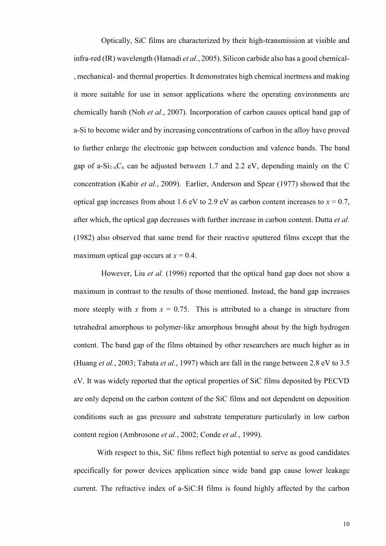
schematic illustration of a-SiC:H proposed by Lee & Bent (2000).
12
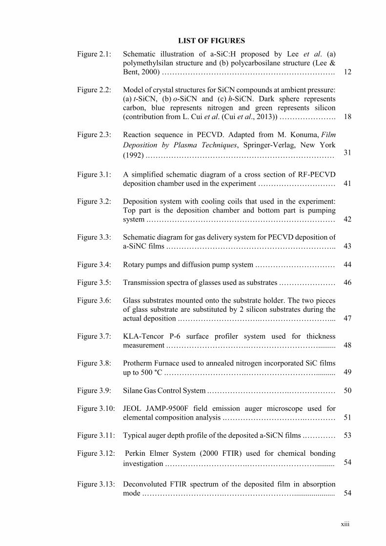
Figure 2.1: Schematic illustration of a-SiC:H proposed by Lee & Bent (2000) (a) polymethylsilan structure and (b) polycarbosilane structure.
2.3.2 Silicon Nitride
Silicon nitride is a hard, dense, refractory material. Amorphous silicon nitride
(a-SiN:H) is extensively used in the microeIectronic industry for a wide variety of
applications including in oxidation mask, dopant diffusion barrier, gate dielectric in field
effect and thin film transistors, coating for III-V semiconductors, interface dielectric
medium, charge storage layer in MNOS non- volatile memories and as a final passivation
layer for device packaging. Typically FTIR spectra for the alloys reveal the presence of
bands for SiHn, NHn and SiN (Della et al., 1985a). Amorphous silicon nitrogen alloys
have optical gap tunable from 1.9 up to 5 eV, depending on nitrogen content (Giorgis et
al., 1997). Increasing N-content also causes enhancement in the radiative efficiency at
room temperature by several orders of magnitude and make emission band blue shifted.
Silicon nitride alloy is therefore very appealing for light emission technology.
Due to its congruent optical properties, it has been used for wide variety of
microelectronic and optoelectronic application such as passivation layers for devise
packaging, diffusion barriers and radiative elements in light–emitting devices (Krimmel
et al., 1991; Sambandam et al., 2005; Xu et al., 2004). The refractive index of the silicon
nitride films can be matched to maximise the light transmission to the active layer of the
13
crystalline solar cells. The stoichiometry of nitride films also varies widely, especially in
plasma deposition, so that refractive index can vary from about 1.8 to 2.2 and is another
useful control parameter for the film deposition.
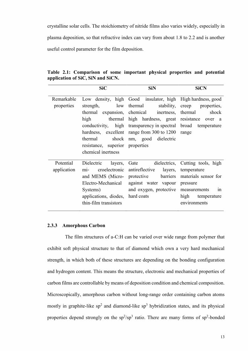
Table 2.1: Comparison of some important physical properties and potential application of SiC, SiN and SiCN.
SiC SiN SiCN
Remarkable properties
Low density, high strength, low thermal expansion, high thermal conductivity, high hardness, excellent thermal shock resistance, superior chemical inertness
Good insulator, high thermal stability, chemical inertness, high hardness, great transparency in spectral range from 300 to 1200 nm, good dielectric properties
High hardness, good creep properties, thermal shock resistance over a broad temperature range
Potential application
Dielectric layers, mi‐ croelectronic and MEMS (Micro-Electro-Mechanical Systems) applications, diodes, thin-film transistors
Gate dielectrics, antireflective layers, protective barriers against water vapour and oxygen, protective hard coats
Cutting tools, high temperature materials sensor for pressure measurements in high temperature environments
2.3.3 Amorphous Carbon
The film structures of a-C:H can be varied over wide range from polymer that
exhibit soft physical structure to that of diamond which own a very hard mechanical
strength, in which both of these structures are depending on the bonding configuration
and hydrogen content. This means the structure, electronic and mechanical properties of
carbon films are controllable by means of deposition condition and chemical composition.
Microscopically, amorphous carbon without long-range order containing carbon atoms
mostly in graphite-like sp2 and diamond-like sp3 hybridization states, and its physical
properties depend strongly on the sp2/sp3 ratio. There are many forms of sp2-bonded
14
carbons with various degrees of graphitic ordering, ranging from microcrystalline
graphite to glassy carbon.
Potential applications for this film are promising in the area of optoelectronic
and microelectronic devices such as light emission diodes and field emission displays.
The optical band gap found by Xu et al. (2004) is reported to be increased between 2.57
eV to 3.3 eV with increasing hydrogen dilution. Only a broad band PL spectrum is found
under the different excitation energies for a sample without hydrogen dilution. With
increasing the hydrogen dilution ratio, the PL peak energy is blue shifted. Demichelis et
al. (1995) and Park et al. (2001) found that the spectra position of the PL peaks do not
exhibit any systematic shifts with increasing optical band gaps of the samples and propose
that the PL peak positions are not correlated with optical band gaps.
2.3.4 Silicon Carbon Nitride
The history SiCN film is rather accidental as compared to that of the SiC itself. After
the failure to produce the super hard CN thin films by many groups (Betranhandy et al.,
2004; Hellgren et al., 1999; Lowther, 1999), the effort was redirected on the development
of SiCN with similar qualities to the properties that possesses by CN. In the early stage
of the work in deposition of SiCN films, element Si that being introduced is aimed to
promote the incorporation of carbon in the formation of CN. In other word SiCN thin
films are unintentionally obtained products during the commencement of the work in
producing CN thin films with desired properties. Also, in the beginning, the study in SiCN
system was mainly geared to syntheses and study the effect of various deposition
condition on the properties of the films (Bendeddouche et al., 1997; Sachdev & Scheid,
2001).
This is aimed to adequately provide detailed understanding of the new material at
the fundamental level in comparison to a very structurally closed compounds and already
15
established SiC and SiN. SiC and SiN have their own super characteristics but it is
suggested that promising features of SiCN would be due to the more complicated Si, C
and N atomic chemical environments in a ternary alloy than in a mixture of pure Si3N4-
SiC phases (Perrin et al., 1996). The area of research in ternary SiCN system is one of the
attractive fields and the knowledge of accessible phases and their microstructure in
precision is still remain lagging and rarely reported for the moment.
The change in the optical properties of a-SiCN with respect to the change of
elemental composition can be viewed in the two different perspectives. Firstly, it is
associated to the compound properties changes with respond to the change in carbon
content while the second perception is related to the change in nitrogen content. In the
first perspectives Chen et al. (2000) have found out that films that have been deposited
with increasing CH4 content indeed have higher contents of C, N and H as an effect which
can be attributed to the presence of SiC and CN bond. The increase in absorption can be
attributed to the presence of carbon. Bulou et al. (2011) discovered that SiN like
compound is dominant at whatever the CH4 rate is used to deposite SiCN films.
CH4 addition leads to less hydrogenated and denser films. In addition, a refractive index
increases from 1.7 to 2.0 and a Tauc gap decrease from 5.2 eV to 4.8 eV is measured with
CH4 rate increase. It is believed that the increase in refractive index is due to higher thin
film density whereas hydrogen bonds decrease is assumed to contribute to the band gap
narrowing.
In the second condition, Peter et al. (2013) reported systematic changes in infrared
actives modes network bonds and optical properties of a-SiCN film following changes in
deposition conditions (nitrogen as well as other parameters). SiCxNy films deposited by
Emarkova et al. (2015) at different ammonia (proportional to concentration of nitrogen
source is presumed) concentration exhibits different transmittance behaviour. High
ammonia dilution led to a rather high transmittance of film, supporting the potential in
16
using the films as highly transparent coatings in optical devises. For comparison purposes,
the refractive index of plasma-deposited silicon carbide ranges from 1.96 to 2.6 and
plasma-deposited silicon nitride from 1.8 to 2.2 (Mort & Jansen, 1986). Refractive index
plays a very important role in the search of material for transmitting light and
manipulating light path for optical applications such as antireflection coating.
Results by Kim et al. (2008) shows that the refractive index of the a-SiCN films
reduces with the increasing NH3 flow rate for which in their case is the source for
nitrogen. The deposited carbon rich films were characterised by the optical band gap in
between 0.6 to 1.5 eV but for nitrogen rich film the band gap energy value can be raised
up to 2.5 eV, which is closed to the Si3N4 energy gap that was obtained. This revealed the
silicon nitride-like nature of the obtained films. The results show regulating nitrogen
versus carbon appears to cause opposite effects at least to optical refractive index and
optical gap of the SiCN films.
Chen et al. (2005) also found a sharp phase transition from the predominantly Si-
C bonded structure to the Si-N bonded structure occurs during the deposition of SiCN
thin films with and without N incorporation. It was reported by Porada et al. (2013) the
SiCN films deposited with the addition of nitrogen have higher value for both of the
hardness and the Young’s Modulus as compared to those of the films deposited without
addition of nitrogen. It was reasoned that the significant increase in Si-N bond attributes
to the change in the films properties. Thus, the compound can be applied in cutting tools
and high temperature materials.
Reports of successful of synthesizing the films and demonstration of interesting
properties are good indicators for the future technological development of the films and
its progress in its fundamental view point. In order to illustrate the point, it has been
proven by Kaltenpoth et al. (2002) that a-SiCN synthesis by RF CVD using organic
precursors methane, silane and ammonia/nitrogen has moisture barrier properties surpass
17
the performance that have shown by reliable moisture barrier silicon nitride and silicon
carbide films. A good barrier layer should possess certain characteristics such as
exhibiting a dense surface morphology without cracks and pinholes, good adhesion to the
substrate, low stress, uniform thickness, reproducible and controllable deposition.
The structure of ternary SiCN compound is predicted to be more complex as
compared to binary SiC due to the addition of the third element in the former compound,
which cause larger number of bonding structures presence within the compound and
detailed study on the corresponding properties especially on the aforementioned chemical
bonding networks had been reported by Wydeven & Kawabe (2009) and Chen et al.
(2004). In the report by Wydeven & Kawabe (2009), various spectroscopy techniques are
used to investigate the nature of carbon- and silicon-nitride network in the as-prepared
thin films. On the other hand, Chen et al. (2004) found out that the phase transition from
SiC to SiN is in which the main reason is ascribed to higher content of nitrogen
concentration during thin film due to high tendency of Si to form bonding with N rather
than C that generally exist in environment. Their calculations using the first principle
show that bond energy can govern the relative stability of Si-N bond for the simple SiCN
clusters. The local atomic structure with Si–N–C (or Si–N=C) bonding exhibits a
considerably lower total energy of 0.65 (0.52) eV than that with Si–C–N (Si–C=N)
bonding, providing the explanation of the stronger affinity of Si–N bonds than Si–C bonds
in the a-SiCN thin films.
Kawamura (1965) had proposed a cubic SiCN (or c-SiCN) phase based on the
β-SiC and indicated that N atoms enter the interstitial sites surrounded by four silicon
atoms. In 1997, two crystalline SiCN compound namely cubic SiC2N4 and orthorhombic
Si2CN4 were synthesised at ambient pressure. A year later Chang et al. (1998) suggested
that SiCN demonstrated similar local bonding structure to α-Si3N4 with substitution of C
atoms only for the silicon sites. Recently, Cui et al. (2013) predicted that SiCN
18
compounds can exist to be relatively stable with a stoichiometry ratio of 1:1:1 at an
ambient pressure.
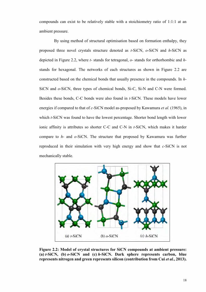
By using method of structural optimisation based on formation enthalpy, they
proposed three novel crystals structure denoted as t-SiCN, o-SiCN and h-SiCN as
depicted in Figure 2.2, where t- stands for tetragonal, o- stands for orthorhombic and h-
stands for hexagonal. The networks of each structures as shown in Figure 2.2 are
constructed based on the chemical bonds that usually presence in the compounds. In h-
SiCN and o-SiCN, three types of chemical bonds, Si-C, Si-N and C-N were formed.
Besides these bonds, C-C bonds were also found in t-SiCN. These models have lower
energies if compared to that of c-SiCN model as-proposed by Kawamura et al. (1965), in
which t-SiCN was found to have the lowest percentage. Shorter bond length with lower
ionic affinity is attributes so shorter C-C and C-N in t-SiCN, which makes it harder
compare to h- and o-SiCN. The structure that proposed by Kawamura was further
reproduced in their simulation with very high energy and show that c-SiCN is not
mechanically stable.
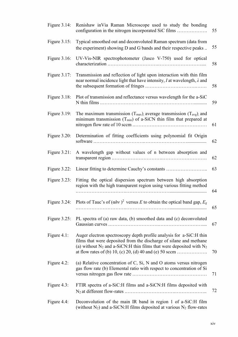
Figure 2.2: Model of crystal structures for SiCN compounds at ambient pressure: (a) t-SiCN, (b) o-SiCN and (c) h-SiCN. Dark sphere represents carbon, blue represents nitrogen and green represents silicon (contribution from Cui et al., 2013).
19
Recently, tribology test was used to investigate the crystal structures of the SiCN. (Xu et
al., 2010) had synthesised two crystalline solids that comprised of c-SiC2N4 (space
group, Pn3m) and o-Si2CN4 (space group, Aba2) by pyrolysis of polyorganosilazanes at
ambient pressure and they reported that the calculated Vickers hardness (HV) values of
the cubic and orthorhombic for the compounds are 16.9 and 28.2 GPa, respectively. Long
chains of Si–N═C═N–Si fragments in Pn3m-structured SiC2N4 and Aba2-structured
Si2CN4 are proposed for the compounds which limit their hardness (Green et al., 2015)
have reported that hexagonal SiCN crystals with 35–40 % N-content and various extents
of Si substitution are wide band gap (3.2–3.8 eV) materials. Theoretical structure analysis
on the crystal structure of SiCN is used to predict stable or metastable structures. It was
found that the stable SiCN phase at ambient pressure was a t-SiCN structure (P42nm,
denoted as t-SiCN) instead of c-SiCN. Two potential phase transitions at 21.6 and 21.9
GPa were proposed. Two high-pressure phases, namely, an orthorhombic structure
(Pnma, denoted as o-SiCN) and a hexagonal structure (R3m, denoted as h-SiCN) showed
interesting properties for industrial applications.
2. 4 Structural and Optical Properties of SiCN
2.4.1 Composition of a-SiCN
Compositionally Si, C, N and O are typical elements found in the SiCN
compounds measured using either using AES or XPS. Since the content of N and C in the
SiCN films are major factors that determined films properties so the change of these
elements content in the films becomes the main focus of the structural studies of the
compound. As such the change in the intensity of bonding especially the bonding of Si-
N and Si-C are critical in the studies as they are related to the two elements. An obvious
increase in the bonding intensity of the two fundamental bonding in SiCN films are
observed to be attributed to an increase in flow rate or concentration of the respective
20
elemental source in deposition chamber (Green et al., 2015). In case of PECVD
technique, using gasses as precursors the elemental sources for N can be either nitrogen
gas or ammonia compound where as for C is largely methane or ethane (Awad et al.,
2010). Also in the same reference it is shown that a-SiCN thin films synthesis using RF
PECVD using gas mixture allowing control on the concentration of elements for
optimisation of composition of the deposited films. It shows that the oxide contaminant
is independent of methane concentration but depend on the flow rate of the reactant gas
composition. Films deposited at higher flow rate (183 ml/min vs. 164 ml/min) has smaller
bulk O concentration (around 2.8 atomic %). It is also very clear that there is generally
no correlation between the elemental composition (ratio form) of the film and the
reactants.
2.4.2 Chemical Bonding
Basically, a mixture of Si, C and N from gas sources produce multiphase
structures for the formation of ternary SiCN compound. These structures are formed from
various chemical bonding presence in SiCN thin films prepared using various methods.
Generally the bonding presence in the films comprises of Si-C, Si-N, C-C, Si-O, C-N. N-
H (Nitriles), C≡N, Si-H, C-H and weak bond of Si-Si is sometimes presence the samples.
It was observed that the presence of chemical bonding structures and the compositions
and their distribution of each element forming the SiCN films are sensitive to deposition
conditions (parameters) as well as the technique of preparation used as discussed in earlier
chapter.
Awad et al. (2010) also reported FTIR and XPS data collected from a-SiCN films
synthesised using vapour transport CVD technique. DPMS was used as a single source
for Si and C and NH3 added as the N source. Analysis on both data indicate the films have
similar presence of major chemical bonding in a-SiCN (Si-C, Si-N, C-N, C-N, C=N) films
21
but varies in minor bonding (such as C≡N, N-H). This to demonstrate the chemical
bonding in the amorphous matrix is more complicated than a collection of single Si-C,
Si-N or Si-H bond. Study made by Zhou et al. (2010) shows that the film structure of a-
SiCN including optical properties are obviously modified readily by controlling the
nitrogen flow. The authors studied the change of properties in term of shift of the
stretching mode for Si-H bond to higher wavenumber as the nitrogen flow ratio increases.
Saloum & Alkhaled (2011) reveal chemical bonding presence in a-SiCN films;
Si-N, Si-C, Si-O and NH, CH3, C=O, Si-H, C-H and O-H. The authors discovered that
the intensity of C-H organic bond decreases rapidly upon switching the feed gas from
argon to nitrogen. It shows the function of nitrogen in decreasing the polymerisation of
organic radicals due to high reactivity of atom nitrogen with precursors, which results in
breaking these bonds and formation of volatile compounds. N-H bond was observed to
increase, accompanied by the vanishing of Si-C bond and the rapid diminishes of C-H
intensity in the film with nitrogen as feeder gas which may be attribute to the insertion of
NH, formed in the plasma after the decomposition of nitrogen and hydrogen from their
precursors into the Si-C bonds. The effect of increasing RF power on the film structure
was also discussed. The peak integrated intensity of Si-N was found increase with
increasing RF power but the intensities of CH organic group and N-H band decrease.
Increasing the RF power causes higher density of nitrogen atom in plasma as well as
electrons becomes more energetic thus increasing collision with precursor and therefore
enhance the Si-N intensity. Unlike the Si-N bond, the intensities of C-H and N-H bands
were found to decrease with RF power increases. This is attributed to the larger breaking
up of these bonds in plasma phase at higher RF plasma power as a result of inelastic
collision with more energetic electron and active nitrogen.
Peng et al. (2009) synthesised dense, hard and very thin a-SiCN films which has
potential use for magnetic storage using MW-ECR plasma enhanced unbalanced
22
magnetron sputtering. Separate target of pure graphite and crystalline silicon in nitrogen
gas (reactive gas) are used as elemental sources of the will be deposited element materials.
High purity argon was used as sputtering gas. The authors suggested that the film structure
should be considered as local Si3N4 and SiC bonds dispersed into the amorphous carbon
substrate, which form a very complicated network. The average composition of the film
is Si29C48N23, which is nearly SiC2N.
Assisting nitrogen ion beam energy and nitrogen concentration of ion beam are
two are deposition process parameters in ion beam sputtering. When these parameters are
increased, Zhou et al. (2010) found that the bonding structures of SiCN films change from
Si-C, Si-N, C=N bonds to Si-C, Si-O, Si-N, C=C, C-N, C=N bonds and showed the mixed
sp2-sp3 hybridized bonds linked with Si(CH4), Si(N4) and Si(C4-nNn) tetrahedral units.
The authors correlated the mechanical properties of the films to the proportion of Si-C,
Si-N, C=N and C-N bonds in the SiCN films. For instance the hardness of the thin film
is found to be linear dependent with Si-C bond density. Thus the C-rich films possesses
the higher value of mechanical properties compared to N- rich SiCN films. Interestingly
C-rich SiCN film, the C-N bond was negligible while the proportion of Si-C bond was
highest. For the N-rich SiCN films, Si bonded with C was substituted by N to form C-N
and C=N bonds and on the other hand, C bonded with Si was substituted by N to gives
Si-N bonds. Lo et al. (2001) showed that the deposited a-SiCN is without Si-C and Si-O
bonds when SiCN films are prepared from SiC/Si/C laminated target sputtering by
nitrogen ion beam. Chen et al. (2005 & 2000) also showed that the a-SiCN is absent of
Si-C when the films were deposited a temperature below 100 °C from an adenine-silicon
mixture target sputtering by Ar ion beam.
Analysis on a-SiCN thin films deposited from polymerised HMDSN by Vassallo
et al. (2006) reveals important bands associated Si-N, Si-C, Si-H, Si-O, C-H with
structures plus other organics molecules. However, when RF power increases molecules
23
such as N-H, Si-CH3, C-H where found to diminish suggesting fragmentation of the
monomer that causes hydrogen extraction. This is confirmed by the appearance of CH2
group in the films. An increase in concentration of unsaturated dangling bonds in films
deposited at higher RF power is also proposed. Ivashchenko et al. (2008) compare the
main bonding in amorphous SiC and SiCN and found that only Si-N and C-N lacks in the
latter films. Also silicon cluster or Si-Si is only detected in SiC but could not be found in
SiCN. Increasing discharge power from 5 W to 30 W causes enhancement of some
chemical bonding in SiCN films. The authors reasoned that an increase in discharge
power is expected to lead to more nitrogen incorporation, and correspondingly to an
enhancement of the Si-C, Si-N and the C-N vibrations. Swain et al. (2006) and Swain &
Dusane (2007) deposited by hot filament CVD using SiH4, CH4, NH3 and H2 precursors.
Increasing the H2 flow rate in the precursors gas, more carbon is introduced into a-SiCN:H
in network resulting in decrease of the silicon content in the film. Detail analysis indicates
that the hydrogen atom contribute mainly to the presence of graphite like carbon network,
increasing sp2 bonded cluster size.
2.4.3 Microstructure of a-SiCN
On the carbon signature, Bendeddouche et al. (1999) observed the Raman
spectrum on the SiC films exhibited a broadband peak at 1420 cm-1 and on SiCN films at
1470 cm-1. In SiC this carbon signature (C- C) presents as network of tetrahedral-trigonal
bonding carbon (mixed sp2-sp3 hybridised bonds). C-C and C-N of sp2-carbon in the a-
SiCN material usually marked its presence as D and G bands in Raman spectra at
approximately 1350 cm-1 and 1600 cm-1 as pointed by Ferrari & Robertson (2000). D
peaks is a characteristic feature of disordered carbon- sp2 atom in rings, while G peak
indicates that the sample contains sp2 cluster, stretching of sp2 in chains and rings. This
can be seen in many a-SiCN samples deposited using various technique as in Zhou et al.
24
(2010) report. The bond is not FTIR active but in few cases the presence of nitrogen
causes breaking bonding symmetry and activate the bonds as in Afanasyev-Charkin &
Nastasi (2004) and Swain & Hwang (2008). Films from PECVD synthesis using
organosilicon compounds as precursor by Ermakova et al. (2015) shows two
characteristic absorption peaks in the Raman spectra, D peak is at 1340 cm-1 and G peak
is at 1580 cm-1.
ID/IG ratio for the carbon shows decreases monotonically with increasing
ammonia partial pressure, accompanied by an increase of N/Si. This means that carbon
cluster sizes decrease as the initial reactive mixture became richer in ammonia. a-SiCN;H
films deposited by hot wire chemical vapour deposition reported by Swain (2006) shows
Raman signatures for wider groups of bonds including silicon and carbon-nitrogen
network with different H2 flow rate. Besides the G and D peaks appearing at 1625 cm-1
and 1350 cm-1 respectively, is the signature of T peak appearing at 1150 cm-1. T peak is
related to the sp3 carbon therefore IT/IG could be associated with the sp3 carbon content
in the a-SiCN;H network. The IT/IG increases at low H2 flow-rate while it decreases at
higher H2 flow-rate indicate increasing sp3 carbon incorporation at low H2 dilution while
it decreases at higher H2 flow rate. An increase in ID/IG monotonically with an increase in
H2 dilution indicates that the hydrogen atoms contributes mainly to incorporation of
graphite- like carbon network, increasing sp2 bonded carbon cluster sizes.
2.4.4 Optical Properties
Saito and Nakaaki (2001) show that by introducing a small amount of nitrogen
during SiC deposition in order to produce silicon carbon nitride, SiCN films by technique
that involves low temperatures reduces the structural disorder and the density of defects,
whereas the optical band gap remains constant for a wide range of nitrogen addition.
Ermakova et al. (2015) shows the transmittance of SiCN films increase within the visible
25
spectrum with increasing ammonia dilution due to decreasing graphite phase formation.
The results are consistent with the measurement of the optical gap for the films. The films
deposited with increasing ammonia dilution are characterized by an increasing optical
band gap. Neethirajan (2012) shows the refractive index of SiCN thin films measured
using interferometer varied in the range of 2.5 to 2.2 for 200 °C substrate temperature.
The refractive index decreased with an increase in flow rate of ammonia. This
may be due to the increased nitrogen concentration in the SiCN. However, features
observed from investigation on the SiCN film (Dunn, 2011) makes it clear that the amount
of silicon present in the film plays a critical role in the determination of the optical
constants with the carbon and nitrogen concentration being less important. The film
which has the most nitrogen and least carbon of all the films, does not have the lowest
index due to the increased proportion of silicon. The film which has the lowest index as
not only does it have high nitrogen content, but also the silicon content is much lower
thin film. It highlights the sensitivity of these films to deposition conditions and
demonstrates that a finer grained approach to an analysis of compositional measurements
could be useful.
The value of refractive index decreased with increasing substrate temperature. For
fabrication of micro-mirrors and anti-reflective coatings of solar cell applications, the
refractive index of SiCN can be tuned and tailored (Charles et al., 2013). From a structural
point of view, the analysis revealed that the sp2 carbon character and the C≡N or C=N
bonds increased with the nitrogen percentage in the gas mixture. These effects induced
an increase of the structural disorder and the amount of dangling bonds in the layer bulk.
The optical properties in terms of optical gap (Eg) and Urbach parameter (Eu) were also
determined. Eg was found to increase with nitrogen percentage in the sputtering mixture,
whereas Eu exhibited an opposite behaviour. We also show that the refractive index and
26
the extinction coefficient determined by ellipsometric spectroscopy are sensitive to the
structural modification.
2.4.5 Photoluminescence
As compared to binary silicon based thin films such as SiN and SiO2, investigation
in the photoluminescence spectra of ternary SiCN is in the infant stage. As such a
realisation of working model for the PL emission for the material seems not in very short
distance but requires lot of effort and volume of emission data. Many authors (Chu et al.,
1995; Emeleus & Stewart, 1935; Tabata et al., 2004) relate the emission to the chemical
complexes in the films, which contains Si, O, N, H and C elements. It is proposed that the
origin of the PL is attributed to the presence of multiphase structure of the a-SiCN films
such as Si-C, Si-N, C-N and Si-O. It follows that the existence of radiative recombination
centers such as between band tails in clusters of various structural groups responsible for
the mission (Swain & Dusane, 2006). Involvement of oxygen-related defects in SiO is
also possible (Wu et al., 2014).
Numbers of emission results from SiCN films prepared using HMDS and
HMDSN followed by inorganic precursors were reported. For instance, Niemann &
Bauhofer (1999) and Swain & Dusane (2006) investigated the PL properties of plasma
deposited films from organosilicone precursors where they found that the PL maximum
varies between 490 nm and 410 nm, and attributed this PL to the existence of different
chemical structures such as Si-(CH3)2, Si-(CH3)3 and Si- CH2-Si. Charles et al. (2013)
deposited a-Si CN thin films by a plasma enhanced chemical vapour deposition technique
using hexamethyldisilazane as a main precursor by varying discharge power. The bright
emission from the SiCN films has three peak structures at 530 nm, 600 nm and 720 nm.
The emission band of 530 nm is believed from tail to tail recombination inside the
amorphous Si-C based matrix, whereas two PL peaks in the spectra range 600 nm - 750
27
nm are assigned to Si-C cluster with Si-O bonds. An increase in discharge power causes
an enhancement in surface roughness and improvement in Si-C network which results an
improvement in PL emission. PL measurement of the crystalline SiCN compound grown
by Chen et al. (1998) centred around 3.26 eV which is identified as near band edge
emission, matched very well with material wide direct band gap of 3.8 eV. These optical
results indicate the potential of SiCN for blue-UV based emission technology.
The room temperature photoluminescence (PL) spectra of the deposited a-SiCN
thin films thin films on c-Si wafers under different plasma condition was studied. The
film with argon gas as a feeder gas with RF power 100 W has the lowest PL intensity and
the peak is centred at 495 nm. This followed by a film with nitrogen gas as a feeder gas
with RF power 100 W and peak centre at 548 nm. The highest PL intensity is for film
with RF power 200 W with the peak centre at 541 nm. It appears that the peak intensity
to be well correlated to the ratio of IR band intensity of unsaturated inorganic bond to
saturated organic.
2.5 Reviews on the Deposition Technique of Silicon and Carbon Based Thin Films
2.5.1 Chemical Vapour Deposition
The chemical vapour deposition is a growth technique based on the condensation
of a material from the vapour or gas phase. Among all the possible materials, the growth
of silicon based films still represents the most industrially important application of CVD
process. It is an important industrial process in the manufacture of thick and thin solid
films of advances and photonic material (Arya & Carlson, 2002; Rill et al., 2008). CVD
for silicon process is presently so developed that the quality of the deposited film is very
high and the entire process is also controlled very well. Depending on the conditions of
the process, amorphous, polycrystalline, or single crystalline films can be obtained.
28
Even though this technique is superior to traditional thin-film deposition techniques
such as spin coating and sputtering (PVD) in many ways, there are many open questions
regarding its processes. General understanding is that, there are three physical and
chemical reactions that take place in the CVD process, these are gas phase reaction
followed by surface reaction and the final stage is the desorption and the sputtering of the
films. The material for the film formation is provided by the reactive gases (precursors),
which are transported by a carrier gas to a ‘hot’ zone of the deposition chamber. Before
a reaction can take place, the reactants must be activated in some way to a minimum of
energy necessary to induce the reaction. The most adopted is thermal activation, but
electric discharges, chemical activation and photo activation (light) can also be effective.
In a thermal activated process, the precursor gas is heated up where they are thermally
dissociated into radicals.
2.5.2 Radio Frequency Plasma Enhanced Chemical Vapour Deposition
In radio frequency plasma enhanced chemical vapour deposition (RF-PECVD), a
RF electric field is set-up and maintained through the capacitor plates and accelerates the
plasma electrons. By this way it allows electrons to increase their kinetic energy to the
value necessary for the dissociation of the (almost stationary) neutral molecules of the
reactive gases. Among the electric discharges, the more often used are microwave (i.e.
about 2450 MHz) and radio frequency or known as RF (i.e. about 20 MHz). These
discharges, which are different from thermal activation, which tend to break only the
weaker bonds, cause extensive fragmentation of molecules. In the RF range, electron
energies in the plasma have a Maxwellian distribution in the 0.1 – 20 eV range. These
energies are sufficiently high to excite molecules or break chemical bonds in collisions
between electrons and gas molecules. The high energy electrons in elastically collide with
gas molecules resulting in excitation or ionization and dissociation. Here, the CVD
29
plasma therefore is a mixture of ionized and or excited gasses (radicals), electrons and
neutrals produced by a primary reaction occurs in a gas phase. Figure 2.3 shows the
summarisation of the reaction sequence in PECVD proposed by Konuma (1992). The
following are possible electron-neutral reactions that take place in their plasma:
a) Vibrational excitation: an electron collides with a neutral molecule, which is
excited from ground level to a vibrational excited level.
b) Ionization: an electron collides with a neutral species and ionizes this species. A
positive ion is formed together with an additional electron. Because more energy
is required to ionize a molecule, compared to electron excitation, the threshold
energies will be higher (starting from 10 eV).
c) Dissociation: in this reaction, a neutral molecule is divided in two (or more)
species.
d) Electron attachment: an electron collides with a neutral molecule and creates a
negative ion. The attachment reactions are mainly important in electronegative
discharges like in silane, in which negative ions play an important role. In methane
plasmas, which are electronegative plasma, negative ions are of minor importance
and hence these reactions can be ignored.
In these entire electron reactions, a variety of species (ions, radicals and excited
species) are formed, which will also participate in the plasma chemistry, leading to
neutral-neutral, ion-neutral and ion-ion reactions. Hence, the combination of all the
different electron reactions, together with the plasma chemistry, lead to a complex
plasma, in which species are produced and consumed in a variety of reactions. Methane
is common used precursor to deposit SiCN or other carbide films since it is available in
high purity (Niemann & Bauhofer, 1999). Methane, which is a simple CH4 molecule, has
a simple dissociation pattern but is capable of producing a large number of ionic species,
free radicals and neutral species, mainly through electron impact, neutral - molecule and
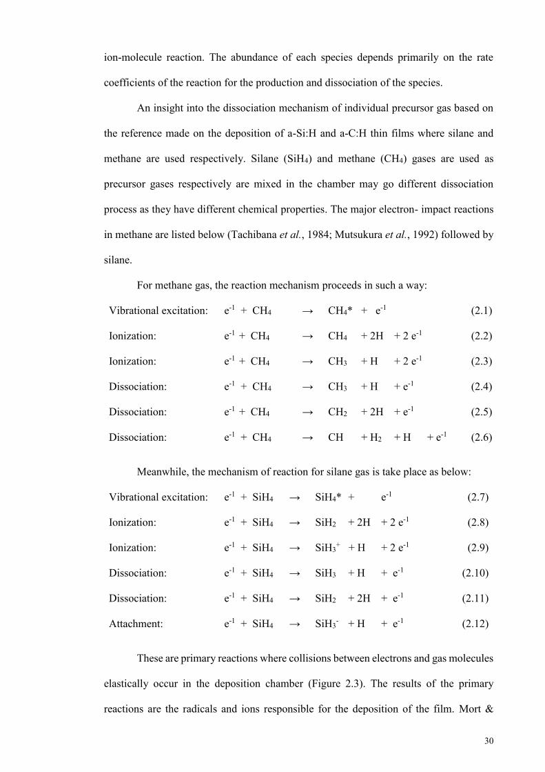
30
ion-molecule reaction. The abundance of each species depends primarily on the rate
coefficients of the reaction for the production and dissociation of the species.
An insight into the dissociation mechanism of individual precursor gas based on
the reference made on the deposition of a-Si:H and a-C:H thin films where silane and
methane are used respectively. Silane (SiH4) and methane (CH4) gases are used as
precursor gases respectively are mixed in the chamber may go different dissociation
process as they have different chemical properties. The major electron- impact reactions
in methane are listed below (Tachibana et al., 1984; Mutsukura et al., 1992) followed by
silane.
For methane gas, the reaction mechanism proceeds in such a way:
Vibrational excitation: e-1 + CH4 → CH4* + e-1 (2.1)
Ionization: e-1 + CH4 → CH4 + 2H + 2 e-1 (2.2)
Ionization: e-1 + CH4 → CH3 + H + 2 e-1 (2.3)
Dissociation: e-1 + CH4 → CH3 + H + e-1 (2.4)
Dissociation: e-1 + CH4 → CH2 + 2H + e-1 (2.5)
Dissociation: e-1 + CH4 → CH + H2 + H + e-1 (2.6)
Meanwhile, the mechanism of reaction for silane gas is take place as below:
Vibrational excitation: e-1 + SiH4 → SiH4* + e-1 (2.7)
Ionization: e-1 + SiH4 → SiH2 + 2H + 2 e-1 (2.8)
Ionization: e-1 + SiH4 → SiH3+ + H + 2 e-1 (2.9)
Dissociation: e-1 + SiH4 → SiH3 + H + e-1 (2.10)
Dissociation: e-1 + SiH4 → SiH2 + 2H + e-1 (2.11)
Attachment: e-1 + SiH4 → SiH3- + H + e-1 (2.12)
These are primary reactions where collisions between electrons and gas molecules
elastically occur in the deposition chamber (Figure 2.3). The results of the primary
reactions are the radicals and ions responsible for the deposition of the film. Mort &
31
Jansen (1986) proposed silane gas is decomposed into reactive neutral radicals (eg. SiH,
SiH2, SiH3, Si2H6, H, H2, etc.) and into positively charged ions (e.g. H+, SiH+, SiH2+,
SiH3+). The neutral radicals diffuse with thermal velocity to all surrounding walls
including the substrate whereas the positive ions are accelerated in the space sheaths in
front of the electrodes leading to a bombardment of the electrodes and the substrate with
positive ions.
Figure 2.3: Reaction sequence in PECVD. Adapted from M. Konuma, Film Deposition by Plasma Techniques, Springer-Verlag, New York (1992).
The principal ionic and radical species in a methane plasma are CH3+ and CH3,
respectively (Green et al., 2015). The CH2 and CH radicals are more active than CH3.
They quickly undergo radical-molecule reactions which make their number densities
lower than that of CH3 radicals (Chen et al., 1998). Hoffmann et al. (2011) made series
of works employing various experimental techniques to thoroughly studied the basics
physicochemical mechanisms in methane plasma responsible for the deposition of
amorphous hydrogenated carbon (a-C:H) films.
The dissociation of precursors produces primary radicals CH3, CH2, CH and C
and the secondary plasma reactions produces unsaturated hydrocarbon radicals, in
particular C2H and C2H3 which also have important role in deposition due to their high
sticking coefficients. It is shown that H atoms and ions can largely enhance the adsorption
32
probability of a given radical through the production of chemisorption sites, especially
dangling bonds, on otherwise hydrogen terminated surface. This effect is especially
marked in the case of CH3, whose sticking coefficient can increase from 10-4 to 10-2.
Instead of this enhancement, the sticking coefficient remains low, and consequently
methyl radicals reach relatively large concentrations in the gas phase but do not usually
play an important role in film growth. The very details of the process are beyond our
research interest and therefore will not be discussed here.
Unlike physical deposition technique, plasma- enhanced CVD utilizes plasma to
enhance chemical reaction rate which relies only on the chemical reaction between ions
in the plasma. The technique allows deposition at lower temperatures, which is often
critical in the manufacture of semiconductors. The lower temperatures also allow for the
deposition of organic coatings, such as plasma polymers, that have been used for
nanoparticle surface functionalization. The characteristics of the (plasma) or discharge
gas are influenced by several parameters, such as frequency of the RF-electric field,
electric power supplied, distance between the two plates and pressure of the gas mixture.
The surface reaction is the other important physical and chemical phenomena
involved in the deposition process based on the CVD technology. An important CVD
process is the mass transport of gaseous species to the growing surface in a field with
non-isothermal flow, the adsorption of the reactants and their diffusion on a solid surface,
the surface reactions and surface migration to attachment sites (kinks and ledges) of the
growing films, and finally the mass transport of gaseous reaction into the gas volume. In
other word, some radicals produced in the gas phase reaction are adsorbed by the
substrate, diffuse on the substrate surface and finally bond with other radicals or re-
evaporate. The condensation from the gas phase can be described by an impinging rate
(Van Sark, 2002):
33
𝑅 =𝑝
2𝜋𝑀𝑘𝐵 𝑇𝑜 (2.13)
where p is the gas pressure, M is the molecular weight of the radicals, 𝑘𝐵 is the
Boltzmann’s constant and T0 is the source temperature. The process of re-evaporation of
the radicals from the surface can be described by a desorption rate with its rate constant
given (Somorjai & Li, 2010) by equation:
ν α eEd
/kB
T (2.14)
where T is the surface temperature and Ed is the activation energy for the desorption
process, which depends from the atomic details of the particular process, i.e. from the
type of radicals involved and from the specific substrate characteristics. Since in
thermodynamic equilibrium all processes proceed in two opposite directions at equal
rates, at equilibrium conditions there should be compensation between condensation and
re-evaporation of the radicals and there would not be a net growth of the film. From this
consideration it is clear that the growth of a film must be a non-equilibrium kinetic
process.
The advantages of using PECVD, among others are:
a) Thin films can be grown over large areas of substrate
b) Low operation temperature
c) Lower chances of cracking deposited layer
d) Good step coverage
e) Due to low T it keeps wafers at low temperatures enhances properties of layers
being deposited
f) Less temperature dependent
The disadvantages of using PECVD are:
a) Not pure film (often lots of H incorporated into film)
b) Plasma damage
34
2.5.3 Microwave PECVD
In the ECR-PECVD technique, the plasma is formed in a separated chamber, called
excitation chamber, where a carrier gas (usually argon) is dissociated or ionized by the
microwave absorption, then the plasma is transferred to another chamber, called
deposition chamber, by diffusion or acceleration by an electric field. The reactive gases
are introduced in the deposition chamber and are dissociated by the plasma electrons,
giving rise to the production of the radicals and the film growth. The advantage of this
separation between the chamber in which the plasma is created and the one in which the
deposition takes place is to avoid a bombardment of the substrate by the plasma ions.
Moreover, a DC or RF bias voltage or a magnetic field can be imposed on the substrate
in order to control the energy of the ions bombarding the surface, without interfering with
the plasma generation.
The limitations related to electromagnetic waves used in RF- PECVD system have
led to the development of a new generation of low-pressure, high-density plasma sources.
Microwave is electromagnetic waves having the frequency range from 300 MHz to 300
GHz. The traditional microwave frequency range is from 1 GHz to 300 GHz. In most
microwaves CVD systems, a microwave generator of frequency 24.5 GHz is used. An
additionally common feature of these sources is the coupling of the microwave power to
the plasma across a dielectric window, rather than direct connection through an electrode
in the plasma. A resonant electromagnetic field is created by microwave generator
(antennae). If an electromagnetic radiation of resonance frequency irradiates the plasma,
it is resonantly absorbed by the electrons, giving rise to a very efficient energy transfer
from the radiation to the plasma: this is called the resonance condition. This non
capacitive power transfer is the key to achieve low voltages across all plasma sheaths at
electrode and wall surface. When operating in the Giga-Hertz (GHz) range, the ions can
be, because of their mass inertia, considered as resting. The electrons absorb energy
35
through electromagnetic waves which lead, in subsequent collisions with the reactive
gases, to heating, ionisation and excitation processes. Another plus point in the system is
that the plasma in the microwaves system is detached from the reactor surface hence no
impurities from reactor construction materials enters the films bulk during deposition.
Some advantages employing the technique:
a) Reduction in radiation damage compared with RF-PECVD. This is because the
microwave discharge results in lower acceleration potential between plasma and
the substrate.
b) It fits for the plasma etching in electronic device processing and possibility of high
resolution etching. This is because plasma is more selective between selective
between photoresist and the underlying material. It causes lower intensity of
radiation damage in reactive ion etching and gives highly anisotropic etching.
c) Microwave plasma is stable, reproducibility, energy efficient, available and
inexpensive magnetrons and potential scaling to large size.
d) Microwave plasma are used in surface treatment so chemical modification and
improve surface bonding are possible
e) Higher electron energy and degree of ionization; higher ion and radical densities.
a) Lower contamination, due to the absence of electrodes.
2.5.4 Hot wire CVD
Another alternative method of depositing SiCN thin film using plasma phase is
hot–wire chemical vapour deposition (HWCVD) based on a catalytic decomposition of
silane or silane hydrogen mixture at a resistively heated filament. This method is
sometimes also denoted as catalytic chemical vapour deposition (Cat-CVD). Hot-wire
CVD was first introduced by Wiesmann et al. (1979) in 1979 when he succeeded to
deposit a-Si:H by thermal decomposition of silane from a hot tungsten or carbon foil
36
heated to about 1600 °C. Unfortunately due to very low gas pressure (1.33 x 10⁻⁶ to 1.33
x 10 -4 mbar), he achieved too low deposition rate (0.6-8.7 A/sec) and films with low
quality due to poor vacuum used.
The process itself and the nature of the produced species on the surface filament
were not understood at that stage. Later, Matsumura & Ihara (1988) obtained high quality
hydro-fluorinated a-Si and hydrogenated amorphous silicon by thermal and catalytic
reactions between deposition-gas and a heated tungsten catalyser. He named it ‘catalytic–
CVD’ method. A deposition rate larger than 20 A/sec was achieved and more importantly,
he reported that the magnitude of the SWE of the films produced seemed smaller than
that of the glow discharge a-SiH produced films. Hot–wire chemical vapour deposition
becomes popular technique for depositing thin film after Hoffmann et al. (2011) had
shown that the method can be further improved the deposition process and produce
superior material performance at the device quality with reduced hydrogen content.
Since then the method has been studied and used mostly at experimental scale
worldwide to deposit thin films. The hot filament (at temperature above 1500 °C)
catalytically excited or cracked the reactant gas into radicals or ions. These radicals
diffuse inside the chamber, react among themselves or deposited onto the substrate placed
few cm away from the filament and heated to an elevated temperature of 150 °C to 450
°C. Since the filament is in the vacuum the heat produced does not directly affect the
process of deposition onto the substrate and this chiefly contribute to the stability of the
deposited films. Feenstra et al. (1999) has confirmed the nature of radicals as exothermic
gas phase reaction in the HWCVD. Some of the advantages of HWCVD technique
including:
a) High deposition rate: For deposition of Si-based thin films high deposition rates
> 10 Å/s can be achieved without the deteriorating their device quality
(Matsumura et al., 2004).
37
b) Ion-free plasma which makes HWCVD a “gentle” process (Mahan, 2003;
Matsumura, et al., 2004).
c) Easily scalable deposition system.
2.6 Ageing (Ageing effects on Si and Carbon based Compound)
References on the ageing of nitrogen incorporated silicon carbide films and are
limited in term of availability and hard to find, an indication the topic is not very widely
researched. However some important factual information for silicon and other films
species which is in the same families to the materials under studies are obtained.
References on films ageing usually will be followed by discussion on the annealing with
one of the purpose is to remove the affects brought by the ageing process. Poitevin et al.
(1982) reported the a-Si:H thin films deposited by DC reactive sputtering in argon-
hydrogen mixture shows the substrate bias influences the film aging effect. The effect
was measured by the evolution of oxygen content in the film which was measured by the
FTIR and RBS after a month air exposure. The results indicated the film deposited at
higher voltage biased are more stable (therefore less O/Si) at room temperature. He
interpreted the results in term of densification of the growing films with the higher bias
voltage due to ion bombardment.
The consequence is that it has better resistance to oxidation induced ageing effect
and increases the refractive index. Tarrach et al. (2008) reported the effect of thermal
ageing on the structural and dielectric properties of the amorphous silicon oxide thin film
(SiO2) composite. The results show that the thermal ageing leads to a structural change,
affects particularly the molecular mobility and increases the dielectric losses. The study
of the dielectric properties showed a space charge relaxation in the studied material. They
also have demonstrated that the heat treatment leads to an improvement in the dielectric
38
properties of the SiOx/SnO material, indeed, the electric conductivity decreases in aged
samples with ageing time.
It was reported by many writers that the films ageing affect physical properties of
the silicon and microcrystalline silicon films. Majority of the researches seem to focus
their attention on the electrical properties of the films as can be seen on few researchers
group (Goodman, 1982; Güneş et al., 2010; Smirnov et al., 2004). They observed and
studied how the films ageing affect films conductivity and the effect of annealing on the
same properties. All writers reported significant change on the films conductivity under
studied induced by adsorbed water and oxygen and found that annealing will remove the
moisture and the adsorbed surrounding component.
2.7 Post Annealing
Since the a-SiCN films in this work is developed using low temperature RF-
PECVD technique, annealing is necessary to acquire information on the effect of high
temperature environment on the films properties and their stability. The investigation
especially of the structural modification induced by heat treatment can help to understand
their structure and improve their properties. There are numbers of process may occur to
the films in the new environment causes them to change their behaviours. Although
structure, optoelectronic and mechanical properties of a-SiCN have been reported,
information on their annealing and effect to films property has been rather limited.
Fernandez-Ramos et al. (2003) studied structural modifications of silicon-doped
carbon nitride (Si-CN) films during post-deposition annealing. The films have Si content
measured below 10 atomic %. The results shows, the thermal behaviour during annealing
of Si-CN films is similar to those reported of pure CN films. They concluded that the
temperature limits for practical use of Si-CN film in air and vacuum atmosphere are 300
°C and 700 °C respectively. Above these temperature, the films are unstable and
39
decompose, releasing nitrogenated species, mainly N2. In air environment, the instability
is featured by the reduction of C=N bonds and the ratio of N/C during the annealing. Aoi
et al. (2001), Fernandez-Ramos et al. (2003) and Hellgren et al. (2001) reported pure CN
films partial graphitation accompanied by nitrogen loss at temperature larger than 500 °C
and become pronounced at temperature above 800 °C.
General view of the effect on the annealing of SiCN is seen on the works Wang
et al. (2007). In this work SiCN films prepared by C+ ion implantations into α-SiN:H
were annealed at three high temperature 800 °C, 1000 °C and 1200 °C and the
photoluminescence spectra from films at different annealing temperature were studied.
The spectra indeed show systematic shift in peak and intensity indicating change in the
composition of emission sources attributed to the change in bonding structures. Si-C, Si-
N, Si-O and SiCN bonds are believed to be sources of the emission but it does not clearly
discuss in specific the breaking or formation of new bonds upon annealing.
Peng et al. (2011) study the effect of annealing on the bonding structure of the
a-SiCN thin films at three different temperatures. Their effort is to relate the resulting
crystallinity and changes in the bonding to the PL properties of the films. In term of
chemical bonding, the intensity of Si-O and Si-C were evidently increased with increasing
temperature (as-deposited to 600 °C and then 800 °C) in the films for annealed films and
found that the Si-C bond decreases with further increase (1100 °C) in temperature. It was
observed that the decrease coincides with the decrease in the intensity of Si-H bond upon
annealing at its early stage and proposed that the decomposition of the Si-H bond is
propitious as Si is needed for the formation of new Si-C bond. However the discussion
stop short in discussing the breaking-up of any particular bonds which provide C for the
formation of the said Si-C bonds. With further increase of annealing temperature the Si-
C bond/crystal also broke down.
40
CHAPTER 3: METHODOLOGY
3.1 Introduction
Thin films of nitrogen incorporated amorphous-silicon carbide (a-SiC) were
deposited at room temperature using home- built deposition chamber using RF-PECVD
technique. The same films then underwent series of temperature annealing up to 400 °C
in the furnace. The pre-annealed and post-annealed films were characterised for their
compositions, structural, optical and photoluminescence (PL) properties. The
composition was measured by AES spectroscopy, the structures was studied by FTIR and
Raman spectroscopy, the optical properties were measured from transmittance and
reflectance obtained by means of UV-VIS and luminescence properties was done by PL
spectroscopy.
The details of the deposition system used, procedures on annealing and the
descriptions on the instrument used for characterisations are presented. Also, the details
on the deposition process including the pumping system, gas delivery system, handling
the silane gas and safety concerns, sample preparation and the technique used in data
analysis for each measurement are reported. Before moving in the details of
characterizations, I first present a brief over view of the RF-PECVD processed used in
the present research work.
3.2 PECVD Deposition System
The home-made PECVD system used in the research work comprises of four main
components which are deposition chamber, gas delivery system, RF generator and
pumping system. The chamber is an air tight stainless steel cylinder of about 30 cm in
radius and height of 60 cm. A schematic diagram of the deposition chamber is shown in
Figure 3.1. The set-up inside the chamber comprises of stainless wire mesh which was
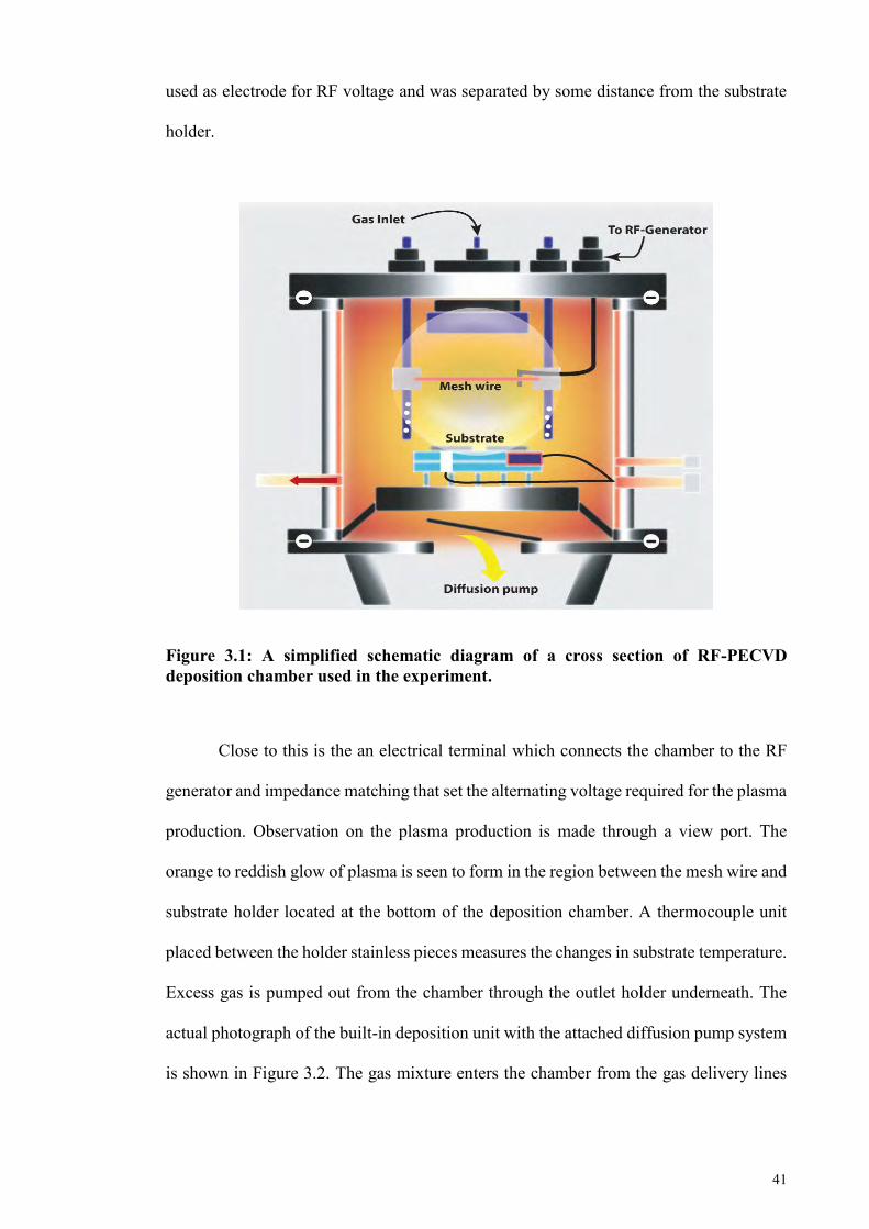
41
used as electrode for RF voltage and was separated by some distance from the substrate
holder.
Figure 3.1: A simplified schematic diagram of a cross section of RF-PECVD deposition chamber used in the experiment.
Close to this is the an electrical terminal which connects the chamber to the RF
generator and impedance matching that set the alternating voltage required for the plasma
production. Observation on the plasma production is made through a view port. The
orange to reddish glow of plasma is seen to form in the region between the mesh wire and
substrate holder located at the bottom of the deposition chamber. A thermocouple unit
placed between the holder stainless pieces measures the changes in substrate temperature.
Excess gas is pumped out from the chamber through the outlet holder underneath. The
actual photograph of the built-in deposition unit with the attached diffusion pump system
is shown in Figure 3.2. The gas mixture enters the chamber from the gas delivery lines
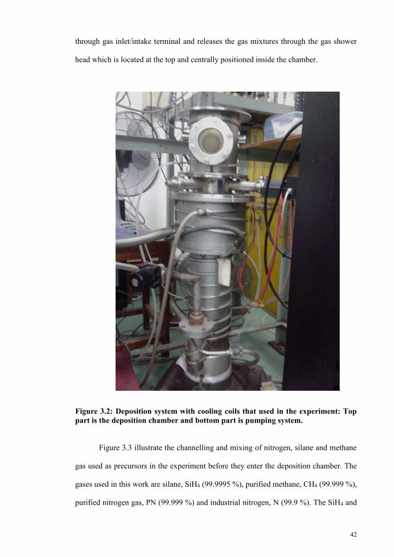
42
through gas inlet/intake terminal and releases the gas mixtures through the gas shower
head which is located at the top and centrally positioned inside the chamber.
Figure 3.2: Deposition system with cooling coils that used in the experiment: Top part is the deposition chamber and bottom part is pumping system.
Figure 3.3 illustrate the channelling and mixing of nitrogen, silane and methane
gas used as precursors in the experiment before they enter the deposition chamber. The
gases used in this work are silane, SiH4 (99.9995 %), purified methane, CH4 (99.999 %),
purified nitrogen gas, PN (99.999 %) and industrial nitrogen, N (99.9 %). The SiH4 and
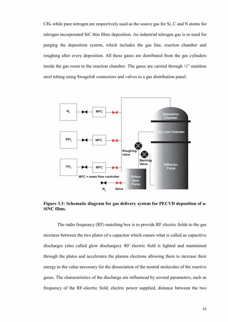
43
CH4 while pure nitrogen are respectively used as the source gas for Si, C and N atoms for
nitrogen incorporated SiC thin films deposition. An industrial nitrogen gas is re-used for
purging the deposition system, which includes the gas line, reaction chamber and
roughing after every deposition. All these gases are distributed from the gas cylinders
inside the gas room to the reaction chamber. The gases are carried through ¼” stainless
steel tubing using Swagelok connectors and valves to a gas distribution panel.
Figure 3.3: Schematic diagram for gas delivery system for PECVD deposition of a-SiNC films.
The radio frequency (RF) matching box is to provide RF electric fields to the gas
mixtures between the two plates of a capacitor which causes what is called as capacitive
discharges (also called glow discharges). RF electric field is lighted and maintained
through the plates and accelerates the plasma electrons allowing them to increase their
energy to the value necessary for the dissociation of the neutral molecules of the reactive
gases. The characteristics of the discharge are influenced by several parameters, such as
frequency of the RF-electric field, electric power supplied, distance between the two
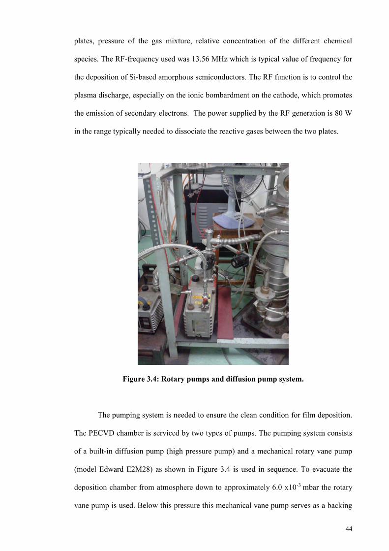
44
plates, pressure of the gas mixture, relative concentration of the different chemical
species. The RF-frequency used was 13.56 MHz which is typical value of frequency for
the deposition of Si-based amorphous semiconductors. The RF function is to control the
plasma discharge, especially on the ionic bombardment on the cathode, which promotes
the emission of secondary electrons. The power supplied by the RF generation is 80 W
in the range typically needed to dissociate the reactive gases between the two plates.
Figure 3.4: Rotary pumps and diffusion pump system.
The pumping system is needed to ensure the clean condition for film deposition.
The PECVD chamber is serviced by two types of pumps. The pumping system consists
of a built-in diffusion pump (high pressure pump) and a mechanical rotary vane pump
(model Edward E2M28) as shown in Figure 3.4 is used in sequence. To evacuate the
deposition chamber from atmosphere down to approximately 6.0 x10⁻³ mbar the rotary
vane pump is used. Below this pressure this mechanical vane pump serves as a backing
45
pump for a built-in diffusion pump capable of reaching pressure as low as of
approximately 2 x 10⁻⁵ mbar is used. The cooling system for the diffusion pump is
circulated by chiller to enhance pumping efficiency of the diffusion pump.
The temperature of the chiller is fixed at 22 °C. The pressure in the chamber for
low and high level vacuum is measured using Pirani (Leybold vacuum gauge with model
TTR91) and Penning (Leybold vacuum gauge with model PTR 225) gauge respectively.
All pumps are purged by nitrogen to protect some of their most sensitive parts and to
avoid possible accumulation of toxic or explosive components when reactive gases are
used.
3.2.1 Thin Film Deposition Procedures
The deposition begins with the substrate preparation. Glass and silicon (Si wafers
of (100) orientation) substrates were used for the deposition of a-SiCN films, depending
on the type of characterization to be performed. For optical and UV transmission
measurements the films were deposited on glass. Glasses of microscope slide were used
as substrate. These glasses are of high transparency (about 90 %) in the required range
for optical studies. Figure 3.5 shows the transmittance from 190 nm – 2500 nm for an
uncoated glass substrate. Note that T = 0 for the glass substrate is in the deep UV,
indicating absorption in this range of the spectrum.
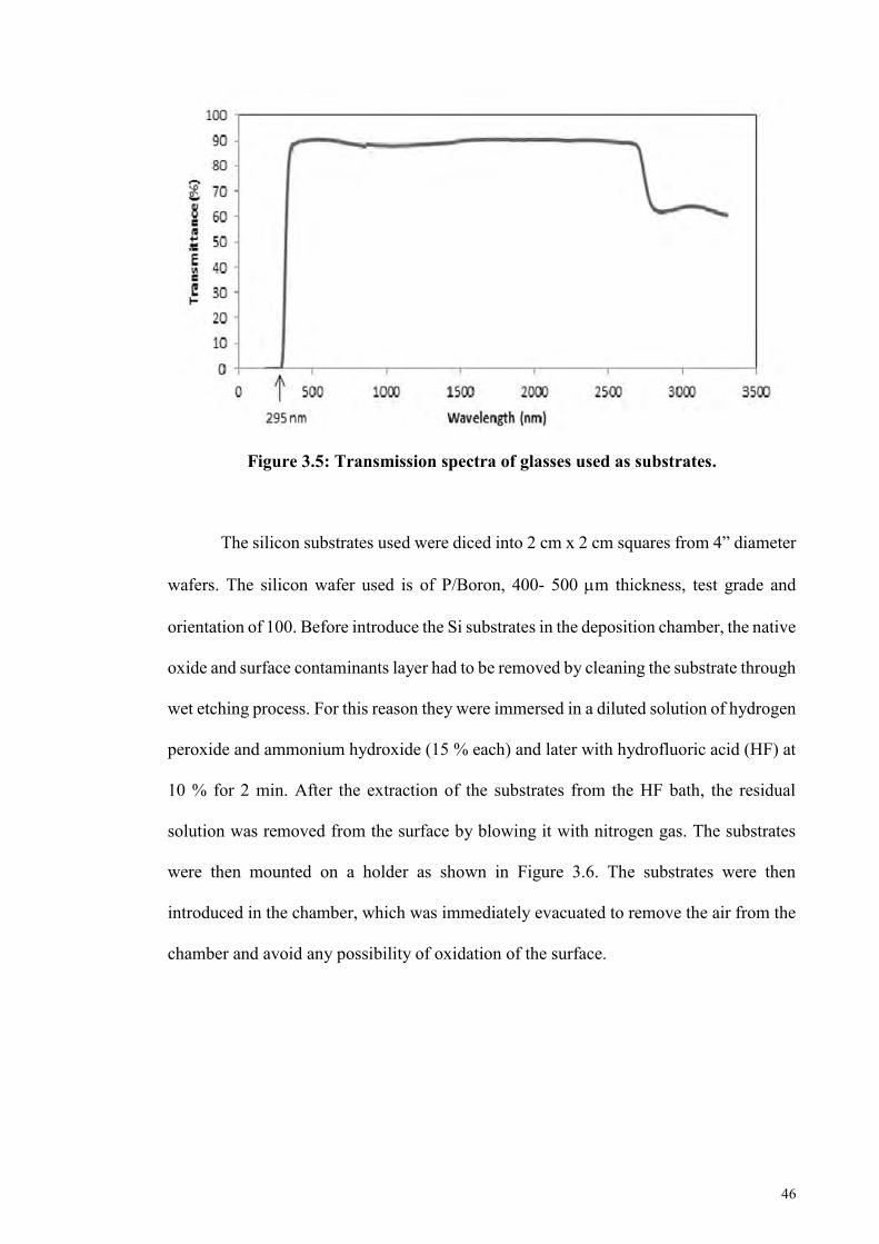
46
Figure 3.5: Transmission spectra of glasses used as substrates.
The silicon substrates used were diced into 2 cm x 2 cm squares from 4” diameter
wafers. The silicon wafer used is of P/Boron, 400- 500 m thickness, test grade and
orientation of 100. Before introduce the Si substrates in the deposition chamber, the native
oxide and surface contaminants layer had to be removed by cleaning the substrate through
wet etching process. For this reason they were immersed in a diluted solution of hydrogen
peroxide and ammonium hydroxide (15 % each) and later with hydrofluoric acid (HF) at
10 % for 2 min. After the extraction of the substrates from the HF bath, the residual
solution was removed from the surface by blowing it with nitrogen gas. The substrates
were then mounted on a holder as shown in Figure 3.6. The substrates were then
introduced in the chamber, which was immediately evacuated to remove the air from the
chamber and avoid any possibility of oxidation of the surface.
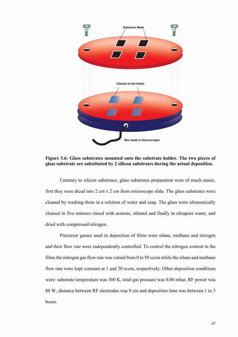
47
Figure 3.6: Glass substrates mounted onto the substrate holder. The two pieces of glass substrate are substituted by 2 silicon substrates during the actual deposition.
Contrary to silicon substrates, glass substrates preparation were of much easier,
first they were diced into 2 cm x 2 cm from microscope slide. The glass substrates were
cleaned by washing them in a solution of water and soap. The glass were ultrasonically
cleaned in five minutes rinsed with acetone, ethanol and finally in ultrapure water, and
dried with compressed nitrogen.
Precursor gasses used in deposition of films were silane, methane and nitrogen
and their flow rate were independently controlled. To control the nitrogen content in the
films the nitrogen gas flow rate was varied from 0 to 50 sccm while the silane and methane
flow rate were kept constant at 1 and 20 sccm, respectively. Other deposition conditions
were: substrate temperature was 300 K, total gas pressure was 0.80 mbar, RF power was
80 W, distance between RF electrodes was 8 cm and deposition time was between 1 to 3
hours.
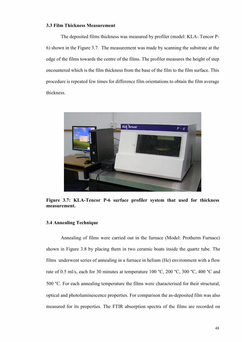
48
3.3 Film Thickness Measurement
The deposited films thickness was measured by profiler (model: KLA- Tencor P-
6) shown in the Figure 3.7. The measurement was made by scanning the substrate at the
edge of the films towards the centre of the films. The profiler measures the height of step
encountered which is the film thickness from the base of the film to the film surface. This
procedure is repeated few times for difference film orientations to obtain the film average
thickness.
Figure 3.7: KLA-Tencor P-6 surface profiler system that used for thickness measurement.
3.4 Annealing Technique
Annealing of films were carried out in the furnace (Model: Protherm Furnace)
shown in Figure 3.8 by placing them in two ceramic boats inside the quartz tube. The
films underwent series of annealing in a furnace in helium (He) environment with a flow
rate of 0.5 ml/s, each for 30 minutes at temperature 100 °C, 200 °C, 300 °C, 400 °C and
500 °C. For each annealing temperature the films were characterised for their structural,
optical and photoluminescence properties. For comparison the as-deposited film was also
measured for its properties. The FTIR absorption spectra of the films are recorded on
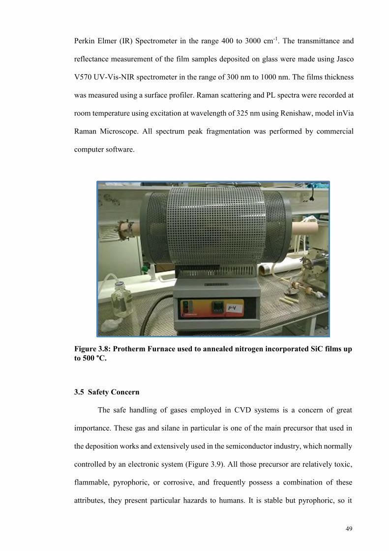
49
Perkin Elmer (IR) Spectrometer in the range 400 to 3000 cm-1. The transmittance and
reflectance measurement of the film samples deposited on glass were made using Jasco
V570 UV-Vis-NIR spectrometer in the range of 300 nm to 1000 nm. The films thickness
was measured using a surface profiler. Raman scattering and PL spectra were recorded at
room temperature using excitation at wavelength of 325 nm using Renishaw, model inVia
Raman Microscope. All spectrum peak fragmentation was performed by commercial
computer software.
Figure 3.8: Protherm Furnace used to annealed nitrogen incorporated SiC films up to 500 °C.
3.5 Safety Concern
The safe handling of gases employed in CVD systems is a concern of great
importance. These gas and silane in particular is one of the main precursor that used in
the deposition works and extensively used in the semiconductor industry, which normally
controlled by an electronic system (Figure 3.9). All those precursor are relatively toxic,
flammable, pyrophoric, or corrosive, and frequently possess a combination of these
attributes, they present particular hazards to humans. It is stable but pyrophoric, so it
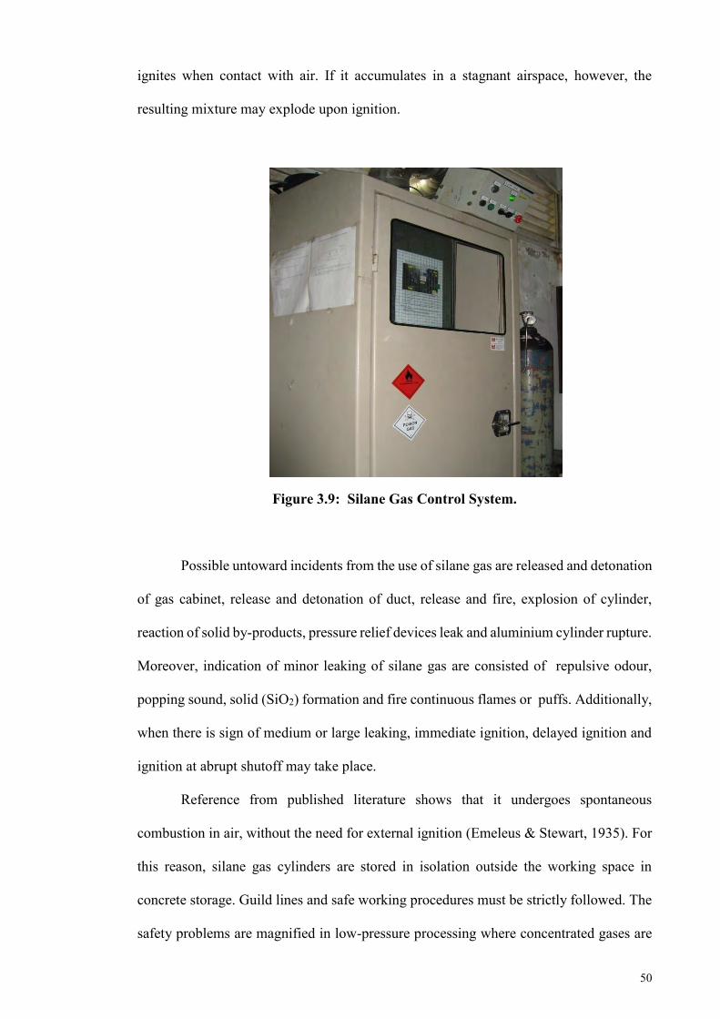
50
ignites when contact with air. If it accumulates in a stagnant airspace, however, the
resulting mixture may explode upon ignition.
Figure 3.9: Silane Gas Control System.
Possible untoward incidents from the use of silane gas are released and detonation
of gas cabinet, release and detonation of duct, release and fire, explosion of cylinder,
reaction of solid by-products, pressure relief devices leak and aluminium cylinder rupture.
Moreover, indication of minor leaking of silane gas are consisted of repulsive odour,
popping sound, solid (SiO2) formation and fire continuous flames or puffs. Additionally,
when there is sign of medium or large leaking, immediate ignition, delayed ignition and
ignition at abrupt shutoff may take place.
Reference from published literature shows that it undergoes spontaneous
combustion in air, without the need for external ignition (Emeleus & Stewart, 1935). For
this reason, silane gas cylinders are stored in isolation outside the working space in
concrete storage. Guild lines and safe working procedures must be strictly followed. The
safety problems are magnified in low-pressure processing where concentrated gases are
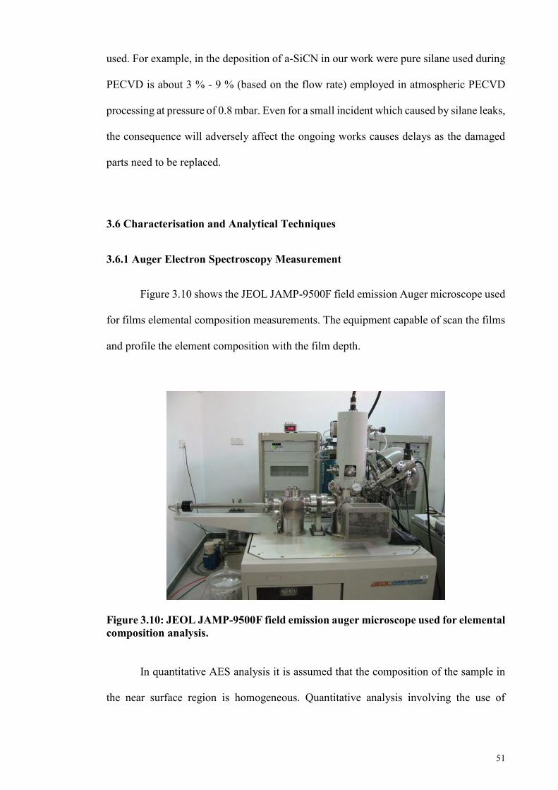
51
used. For example, in the deposition of a-SiCN in our work were pure silane used during
PECVD is about 3 % - 9 % (based on the flow rate) employed in atmospheric PECVD
processing at pressure of 0.8 mbar. Even for a small incident which caused by silane leaks,
the consequence will adversely affect the ongoing works causes delays as the damaged
parts need to be replaced.
3.6 Characterisation and Analytical Techniques
3.6.1 Auger Electron Spectroscopy Measurement
Figure 3.10 shows the JEOL JAMP-9500F field emission Auger microscope used
for films elemental composition measurements. The equipment capable of scan the films
and profile the element composition with the film depth.
Figure 3.10: JEOL JAMP-9500F field emission auger microscope used for elemental composition analysis.
In quantitative AES analysis it is assumed that the composition of the sample in
the near surface region is homogeneous. Quantitative analysis involving the use of
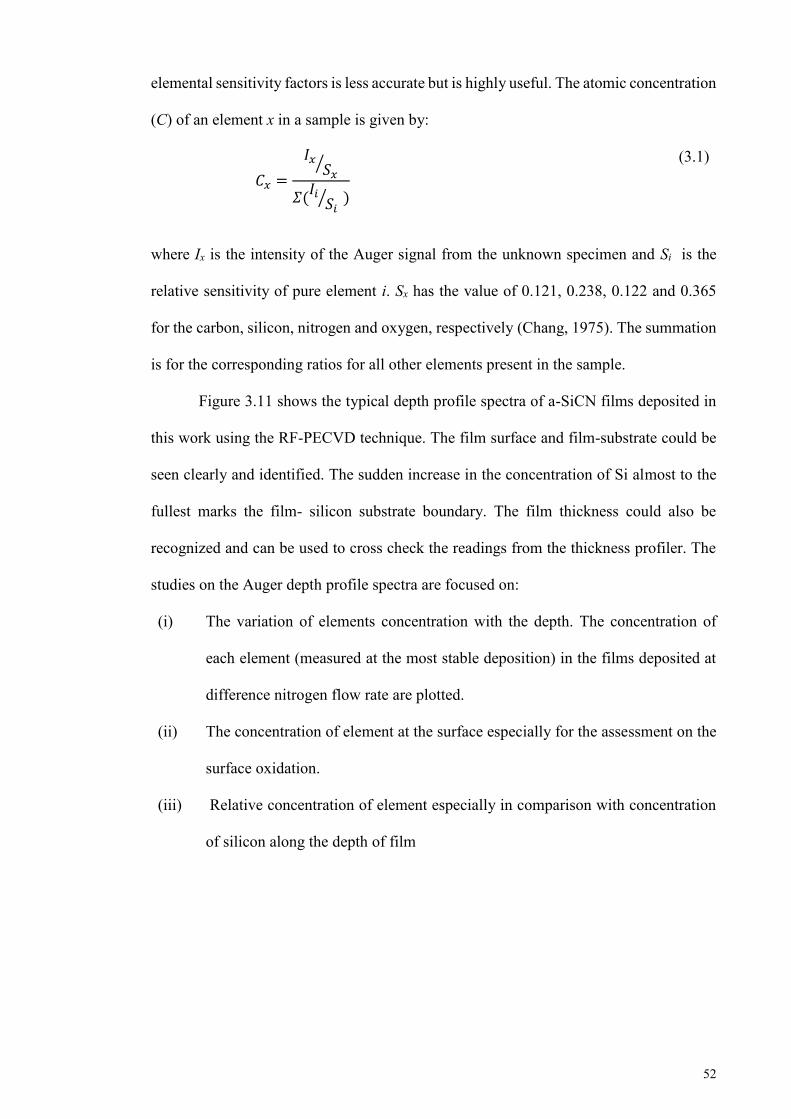
52
elemental sensitivity factors is less accurate but is highly useful. The atomic concentration
(C) of an element x in a sample is given by:
𝐶𝑥 =
𝐼𝑥𝑆𝑥
⁄
𝛴(𝐼𝑖
𝑆𝑖 ⁄ )
(3.1)
where Ix is the intensity of the Auger signal from the unknown specimen and Si is the
relative sensitivity of pure element i. Sx has the value of 0.121, 0.238, 0.122 and 0.365
for the carbon, silicon, nitrogen and oxygen, respectively (Chang, 1975). The summation
is for the corresponding ratios for all other elements present in the sample.
Figure 3.11 shows the typical depth profile spectra of a-SiCN films deposited in
this work using the RF-PECVD technique. The film surface and film-substrate could be
seen clearly and identified. The sudden increase in the concentration of Si almost to the
fullest marks the film- silicon substrate boundary. The film thickness could also be
recognized and can be used to cross check the readings from the thickness profiler. The
studies on the Auger depth profile spectra are focused on:
(i) The variation of elements concentration with the depth. The concentration of
each element (measured at the most stable deposition) in the films deposited at
difference nitrogen flow rate are plotted.
(ii) The concentration of element at the surface especially for the assessment on the
surface oxidation.
(iii) Relative concentration of element especially in comparison with concentration
of silicon along the depth of film
53
Figure 3.11: Typical auger depth profile of the deposited a-SiCN films.
3.6.2 Fourier Transform Infrared Spectroscopy
The infrared (IR) absorption spectra of the films for structure analysis are recorded
on Perkin Elmer (IR) Spectrometer (Figure 3.12) in the range 400 to 3000 cm-1. A spectral
deconvolution fitting process is used to extract the components of the FTIR spectral bands
of the prepared a-SiCN flms. The deconvoluted FTIR spectrum for a deposited sample is
shown in Figure 3.13. The actual deconvoluted FTIR spectrum of the films for the whole
range of wavelength can be seen on Appendix 3. The deconvolution is involves
normalizing the area under the Gaussian curve fitted for each element to its peak value.
The peak values of the of the deconvoluted curves match the presence of vibration mode
of certain bond structure at certain wavenumber in the deposited film. The ratio of the
area under the peak gives the integrated intensity of the bond structures found in the films.
The integrated intensity measures the bond density which is then plotted with the variation
in nitrogen flow rate and analyse.
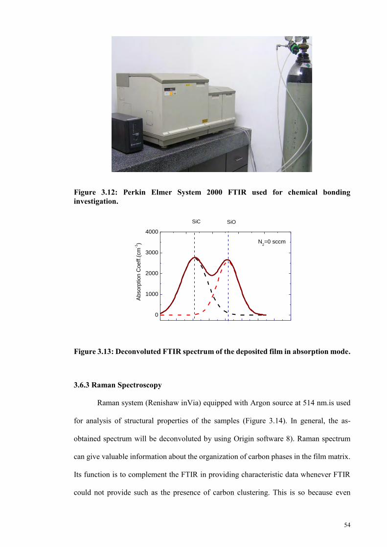
54
Figure 3.12: Perkin Elmer System 2000 FTIR used for chemical bonding investigation.
0
1000
2000
3000
4000
Absorp
tio
n C
oe
ff.(
cm
-1) N
2=0 sccm
SiC SiO
Figure 3.13: Deconvoluted FTIR spectrum of the deposited film in absorption mode.
3.6.3 Raman Spectroscopy
Raman system (Renishaw inVia) equipped with Argon source at 514 nm.is used
for analysis of structural properties of the samples (Figure 3.14). In general, the as-
obtained spectrum will be deconvoluted by using Origin software 8). Raman spectrum
can give valuable information about the organization of carbon phases in the film matrix.
Its function is to complement the FTIR in providing characteristic data whenever FTIR
could not provide such as the presence of carbon clustering. This is so because even
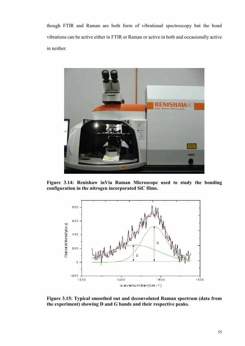
55
though FTIR and Raman are both form of vibrational spectroscopy but the bond
vibrations can be active either in FTIR or Raman or active in both and occasionally active
in neither.
Figure 3.14: Renishaw inVia Raman Microscope used to study the bonding configuration in the nitrogen incorporated SiC films.
Figure 3.15: Typical smoothed out and deconvoluted Raman spectrum (data from the experiment) showing D and G bands and their respective peaks.
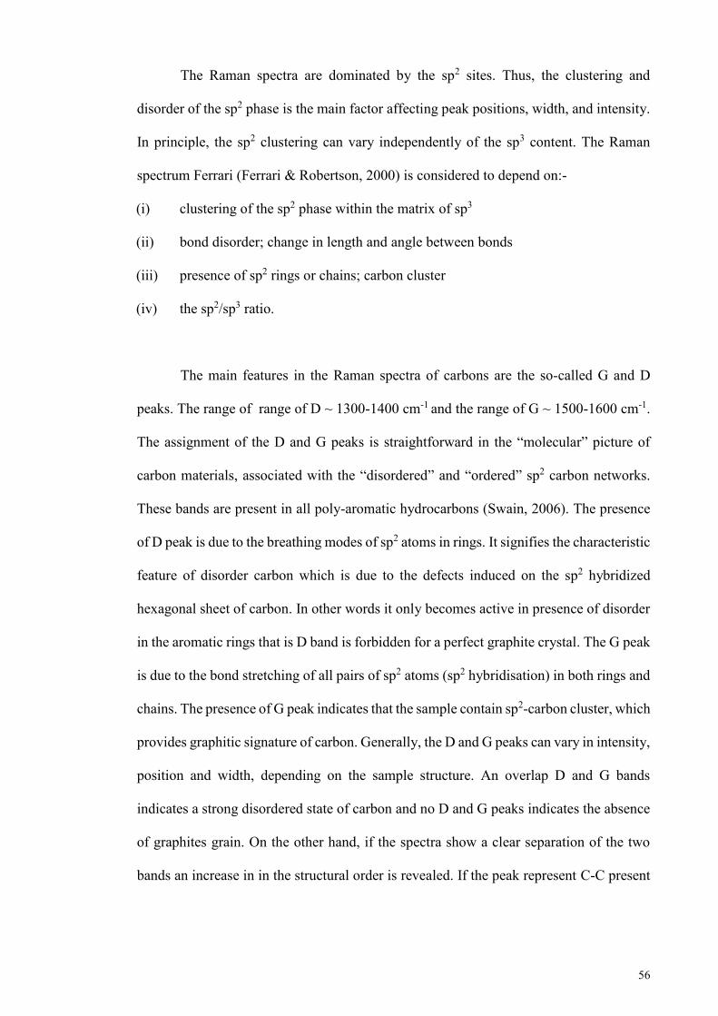
56
The Raman spectra are dominated by the sp2 sites. Thus, the clustering and
disorder of the sp2 phase is the main factor affecting peak positions, width, and intensity.
In principle, the sp2 clustering can vary independently of the sp3 content. The Raman
spectrum Ferrari (Ferrari & Robertson, 2000) is considered to depend on:-
(i) clustering of the sp2 phase within the matrix of sp3
(ii) bond disorder; change in length and angle between bonds
(iii) presence of sp2 rings or chains; carbon cluster
(iv) the sp2/sp3 ratio.
The main features in the Raman spectra of carbons are the so-called G and D
peaks. The range of range of D ~ 1300-1400 cm-1 and the range of G ~ 1500-1600 cm-1.
The assignment of the D and G peaks is straightforward in the “molecular” picture of
carbon materials, associated with the “disordered” and “ordered” sp2 carbon networks.
These bands are present in all poly-aromatic hydrocarbons (Swain, 2006). The presence
of D peak is due to the breathing modes of sp2 atoms in rings. It signifies the characteristic
feature of disorder carbon which is due to the defects induced on the sp2 hybridized
hexagonal sheet of carbon. In other words it only becomes active in presence of disorder
in the aromatic rings that is D band is forbidden for a perfect graphite crystal. The G peak
is due to the bond stretching of all pairs of sp2 atoms (sp2 hybridisation) in both rings and
chains. The presence of G peak indicates that the sample contain sp2-carbon cluster, which
provides graphitic signature of carbon. Generally, the D and G peaks can vary in intensity,
position and width, depending on the sample structure. An overlap D and G bands
indicates a strong disordered state of carbon and no D and G peaks indicates the absence
of graphites grain. On the other hand, if the spectra show a clear separation of the two
bands an increase in in the structural order is revealed. If the peak represent C-C present
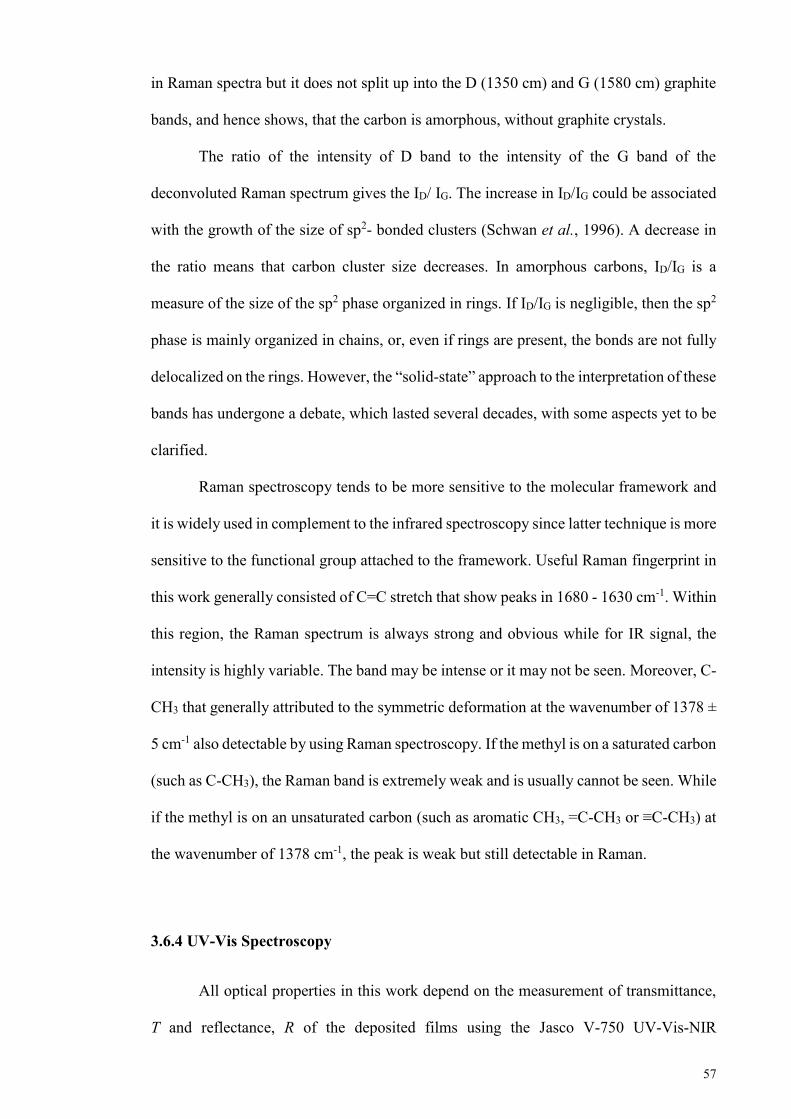
57
in Raman spectra but it does not split up into the D (1350 cm) and G (1580 cm) graphite
bands, and hence shows, that the carbon is amorphous, without graphite crystals.
The ratio of the intensity of D band to the intensity of the G band of the
deconvoluted Raman spectrum gives the ID/ IG. The increase in ID/IG could be associated
with the growth of the size of sp2- bonded clusters (Schwan et al., 1996). A decrease in
the ratio means that carbon cluster size decreases. In amorphous carbons, ID/IG is a
measure of the size of the sp2 phase organized in rings. If ID/IG is negligible, then the sp2
phase is mainly organized in chains, or, even if rings are present, the bonds are not fully
delocalized on the rings. However, the “solid-state” approach to the interpretation of these
bands has undergone a debate, which lasted several decades, with some aspects yet to be
clarified.
Raman spectroscopy tends to be more sensitive to the molecular framework and
it is widely used in complement to the infrared spectroscopy since latter technique is more
sensitive to the functional group attached to the framework. Useful Raman fingerprint in
this work generally consisted of C=C stretch that show peaks in 1680 - 1630 cm-1. Within
this region, the Raman spectrum is always strong and obvious while for IR signal, the
intensity is highly variable. The band may be intense or it may not be seen. Moreover, C-
CH3 that generally attributed to the symmetric deformation at the wavenumber of 1378 ±
5 cm-1 also detectable by using Raman spectroscopy. If the methyl is on a saturated carbon
(such as C-CH3), the Raman band is extremely weak and is usually cannot be seen. While
if the methyl is on an unsaturated carbon (such as aromatic CH3, =C-CH3 or ≡C-CH3) at
the wavenumber of 1378 cm-1, the peak is weak but still detectable in Raman.
3.6.4 UV-Vis Spectroscopy
All optical properties in this work depend on the measurement of transmittance,
T and reflectance, R of the deposited films using the Jasco V-750 UV-Vis-NIR
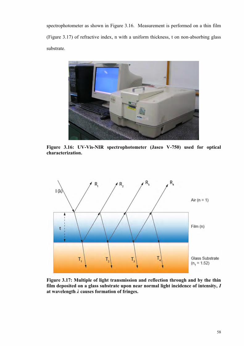
58
spectrophotometer as shown in Figure 3.16. Measurement is performed on a thin film
(Figure 3.17) of refractive index, n with a uniform thickness, t on non-absorbing glass
substrate.
Figure 3.16: UV-Vis-NIR spectrophotometer (Jasco V-750) used for optical characterization.
Figure 3.17: Multiple of light transmission and reflection through and by the thin film deposited on a glass substrate upon near normal light incidence of intensity, I at wavelength λ causes formation of fringes.
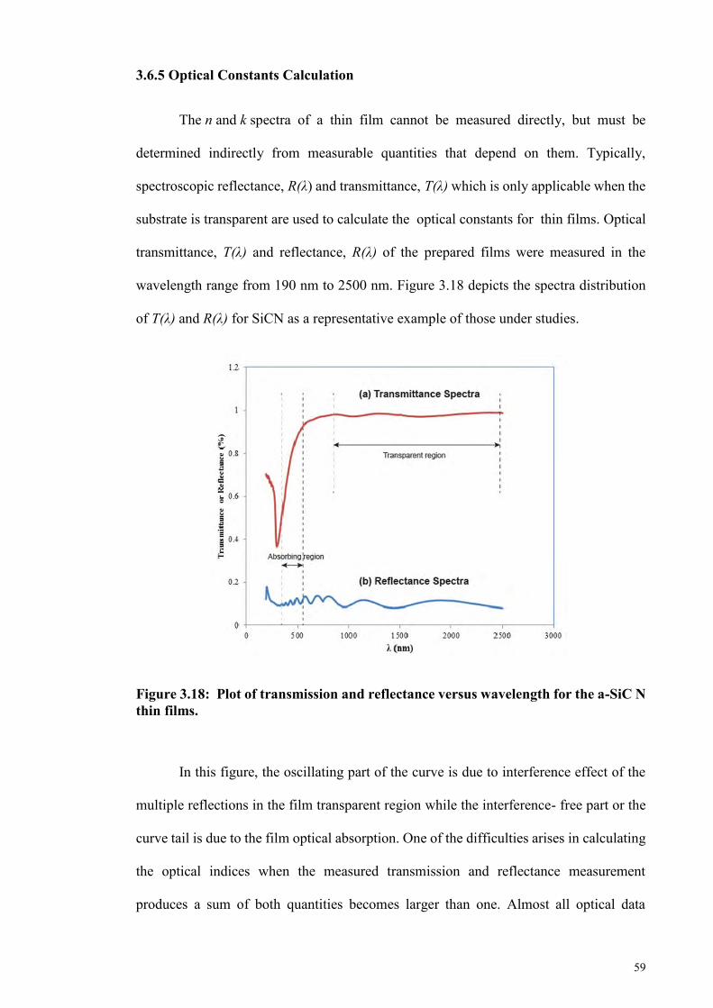
59
3.6.5 Optical Constants Calculation
The n and k spectra of a thin film cannot be measured directly, but must be
determined indirectly from measurable quantities that depend on them. Typically,
spectroscopic reflectance, R(λ) and transmittance, T(λ) which is only applicable when the
substrate is transparent are used to calculate the optical constants for thin films. Optical
transmittance, T(λ) and reflectance, R(λ) of the prepared films were measured in the
wavelength range from 190 nm to 2500 nm. Figure 3.18 depicts the spectra distribution
of T(λ) and R(λ) for SiCN as a representative example of those under studies.
Figure 3.18: Plot of transmission and reflectance versus wavelength for the a-SiC N thin films.
In this figure, the oscillating part of the curve is due to interference effect of the
multiple reflections in the film transparent region while the interference- free part or the
curve tail is due to the film optical absorption. One of the difficulties arises in calculating
the optical indices when the measured transmission and reflectance measurement
produces a sum of both quantities becomes larger than one. Almost all optical data
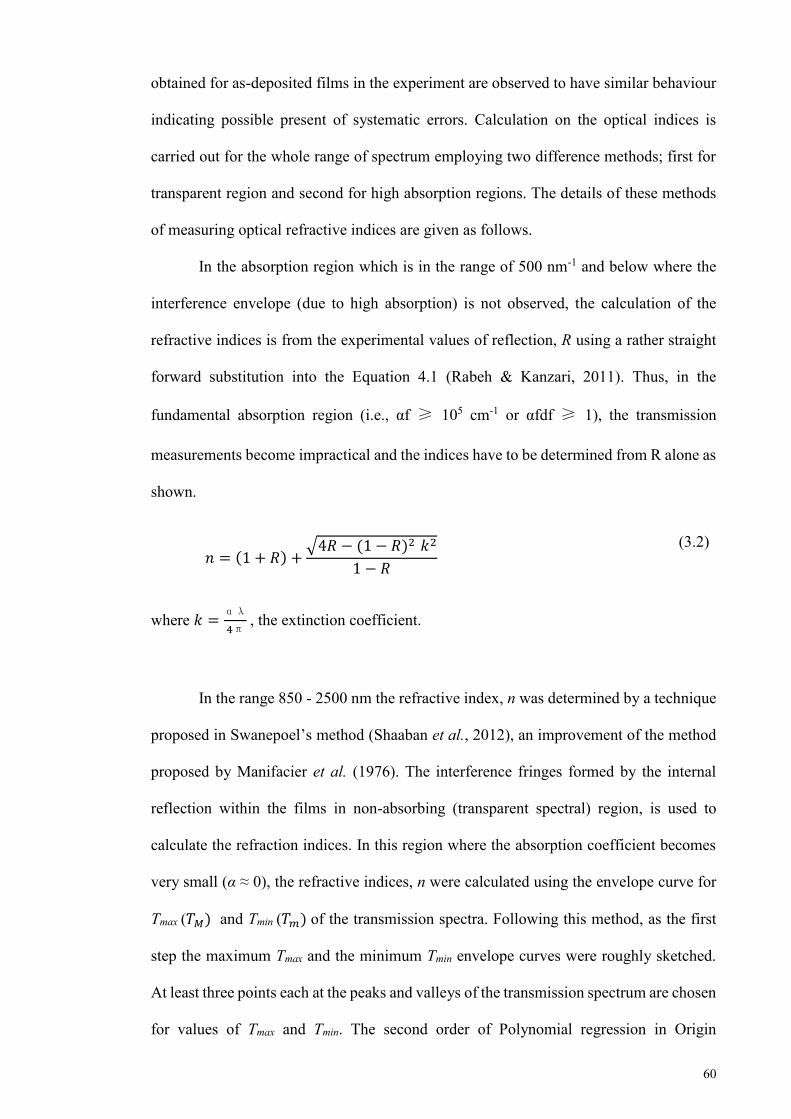
60
obtained for as-deposited films in the experiment are observed to have similar behaviour
indicating possible present of systematic errors. Calculation on the optical indices is
carried out for the whole range of spectrum employing two difference methods; first for
transparent region and second for high absorption regions. The details of these methods
of measuring optical refractive indices are given as follows.
In the absorption region which is in the range of 500 nm-1 and below where the
interference envelope (due to high absorption) is not observed, the calculation of the
refractive indices is from the experimental values of reflection, R using a rather straight
forward substitution into the Equation 4.1 (Rabeh & Kanzari, 2011). Thus, in the
fundamental absorption region (i.e., αf ≥ 105 cm-1 or αfdf ≥ 1), the transmission
measurements become impractical and the indices have to be determined from R alone as
shown.
𝑛 = (1 + 𝑅) +√4𝑅 − (1 − 𝑅)2 𝑘2
1 − 𝑅
(3.2)
where 𝑘 =αλ
4π , the extinction coefficient.
In the range 850 - 2500 nm the refractive index, n was determined by a technique
proposed in Swanepoel’s method (Shaaban et al., 2012), an improvement of the method
proposed by Manifacier et al. (1976). The interference fringes formed by the internal
reflection within the films in non-absorbing (transparent spectral) region, is used to
calculate the refraction indices. In this region where the absorption coefficient becomes
very small (α ≈ 0), the refractive indices, n were calculated using the envelope curve for
Tmax (𝑇𝑀) and Tmin (𝑇𝑚) of the transmission spectra. Following this method, as the first
step the maximum Tmax and the minimum Tmin envelope curves were roughly sketched.
At least three points each at the peaks and valleys of the transmission spectrum are chosen
for values of Tmax and Tmin. The second order of Polynomial regression in Origin
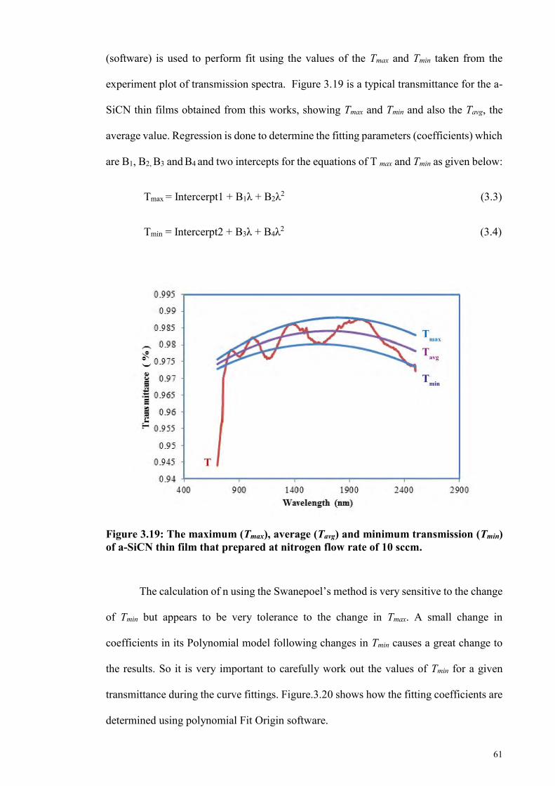
61
(software) is used to perform fit using the values of the Tmax and Tmin taken from the
experiment plot of transmission spectra. Figure 3.19 is a typical transmittance for the a-
SiCN thin films obtained from this works, showing Tmax and Tmin and also the Tavg, the
average value. Regression is done to determine the fitting parameters (coefficients) which
are B1, B2, B3 and B4 and two intercepts for the equations of T max and Tmin as given below:
Tmax = Intercerpt1 + B1λ + B2λ2 (3.3)
Tmin = Intercerpt2 + B3λ + B4λ2 (3.4)
Figure 3.19: The maximum (Tmax), average (Tavg) and minimum transmission (Tmin) of a-SiCN thin film that prepared at nitrogen flow rate of 10 sccm.
The calculation of n using the Swanepoel’s method is very sensitive to the change
of Tmin but appears to be very tolerance to the change in Tmax. A small change in
coefficients in its Polynomial model following changes in Tmin causes a great change to
the results. So it is very important to carefully work out the values of Tmin for a given
transmittance during the curve fittings. Figure.3.20 shows how the fitting coefficients are
determined using polynomial Fit Origin software.
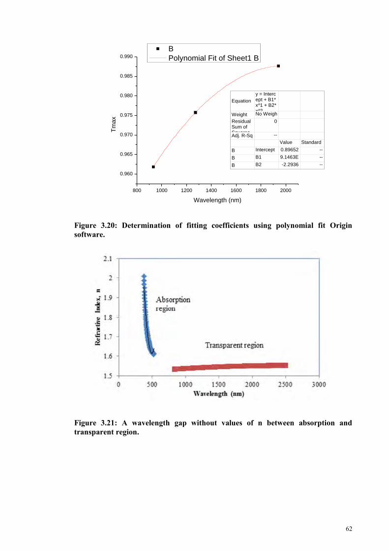
62
800 1000 1200 1400 1600 1800 2000
0.960
0.965
0.970
0.975
0.980
0.985
0.990
B
Polynomial Fit of Sheet1 B
Tm
ax
Wavelength (nm)
Equation
y = Intercept + B1*x^1 + B2*x^2
Weight No Weigh
Residual Sum of Squares
0
Adj. R-Sq --
Value Standard
B Intercept 0.89652 --
B B1 9.1463E --
B B2 -2.2936 --
Figure 3.20: Determination of fitting coefficients using polynomial fit Origin software.
Figure 3.21: A wavelength gap without values of n between absorption and transparent region.
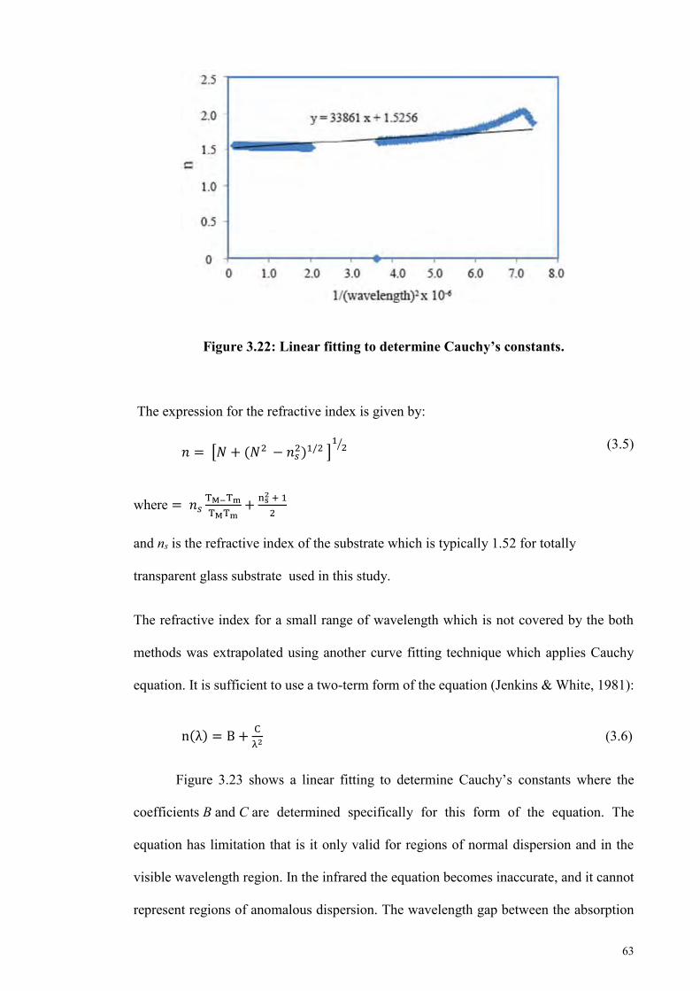
63
Figure 3.22: Linear fitting to determine Cauchy’s constants.
The expression for the refractive index is given by:
𝑛 = [𝑁 + (𝑁2 − 𝑛𝑠2)1/2
]
12⁄ (3.5)
where = 𝑛𝑠TM−Tm
TMTm+
ns2 + 1
2
and ns is the refractive index of the substrate which is typically 1.52 for totally
transparent glass substrate used in this study.
The refractive index for a small range of wavelength which is not covered by the both
methods was extrapolated using another curve fitting technique which applies Cauchy
equation. It is sufficient to use a two-term form of the equation (Jenkins & White, 1981):
n(λ) = B +C
λ2 (3.6)
Figure 3.23 shows a linear fitting to determine Cauchy’s constants where the
coefficients B and C are determined specifically for this form of the equation. The
equation has limitation that is it only valid for regions of normal dispersion and in the
visible wavelength region. In the infrared the equation becomes inaccurate, and it cannot
represent regions of anomalous dispersion. The wavelength gap between the absorption
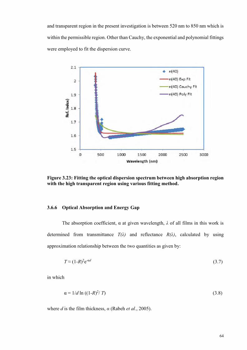
64
and transparent region in the present investigation is between 520 nm to 850 nm which is
within the permissible region. Other than Cauchy, the exponential and polynomial fittings
were employed to fit the dispersion curve.
Figure 3.23: Fitting the optical dispersion spectrum between high absorption region with the high transparent region using various fitting method.
3.6.6 Optical Absorption and Energy Gap
The absorption coefficient, α at given wavelength, λ of all films in this work is
determined from transmittance T(λ) and reflectance R(λ), calculated by using
approximation relationship between the two quantities as given by:
T ≈ (1-R)2e-αd (3.7)
in which
α = 1/d ln ((1-R)2/ T) (3.8)
where d is the film thickness, α (Rabeh et al., 2005).
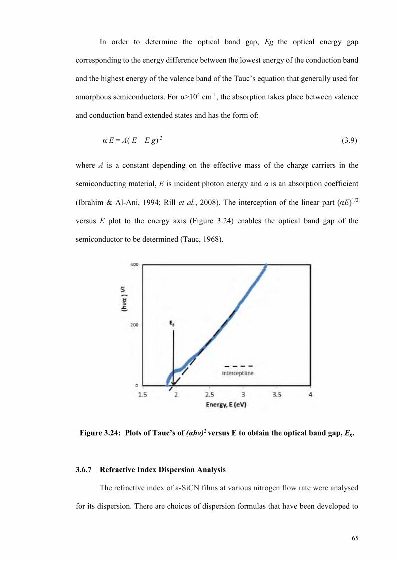
65
In order to determine the optical band gap, Еg the optical energy gap
corresponding to the energy difference between the lowest energy of the conduction band
and the highest energy of the valence band of the Tauc’s equation that generally used for
amorphous semiconductors. For α>104 cm-1, the absorption takes place between valence
and conduction band extended states and has the form of:
α E = A( E – E g) 2 (3.9)
where А is a constant depending on the effective mass of the charge carriers in the
semiconducting material, E is incident photon energy and α is an absorption coefficient
(Ibrahim & Al-Ani, 1994; Rill et al., 2008). The interception of the linear part (αE)1/2
versus E plot to the energy axis (Figure 3.24) enables the optical band gap of the
semiconductor to be determined (Tauc, 1968).
Figure 3.24: Plots of Tauc’s of (αhν)2 versus E to obtain the optical band gap, Eg.
3.6.7 Refractive Index Dispersion Analysis
The refractive index of a-SiCN films at various nitrogen flow rate were analysed
for its dispersion. There are choices of dispersion formulas that have been developed to
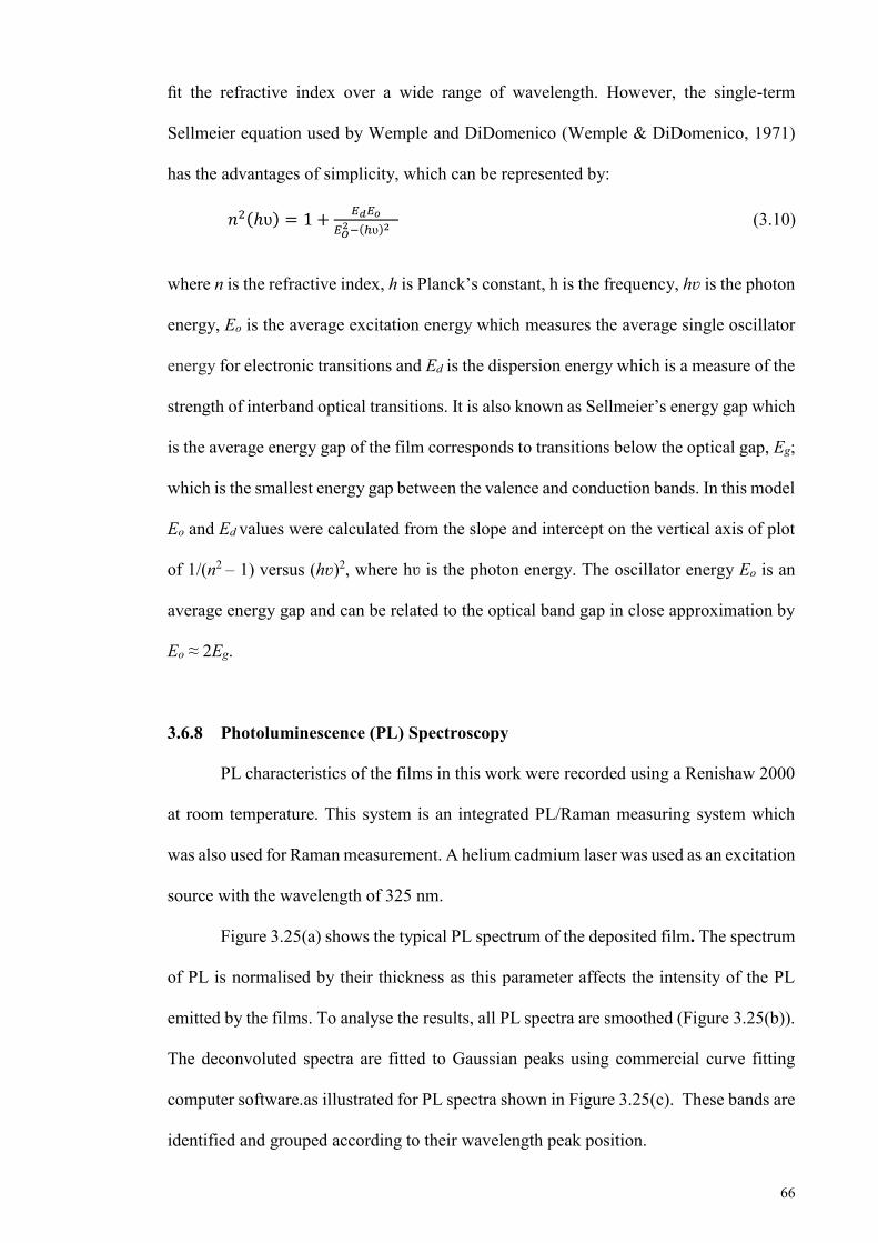
66
fit the refractive index over a wide range of wavelength. However, the single-term
Sellmeier equation used by Wemple and DiDomenico (Wemple & DiDomenico, 1971)
has the advantages of simplicity, which can be represented by:
𝑛2(ℎʋ) = 1 +𝐸𝑑𝐸𝑜
𝐸𝑂2 −(ℎʋ)2
(3.10)
where n is the refractive index, h is Planck’s constant, h is the frequency, hʋ is the photon
energy, Eo is the average excitation energy which measures the average single oscillator
energy for electronic transitions and Ed is the dispersion energy which is a measure of the
strength of interband optical transitions. It is also known as Sellmeier’s energy gap which
is the average energy gap of the film corresponds to transitions below the optical gap, Eg;
which is the smallest energy gap between the valence and conduction bands. In this model
Eo and Ed values were calculated from the slope and intercept on the vertical axis of plot
of 1/(n2 – 1) versus (hʋ)2, where hʋ is the photon energy. The oscillator energy Eo is an
average energy gap and can be related to the optical band gap in close approximation by
Eo ≈ 2Eg.
3.6.8 Photoluminescence (PL) Spectroscopy
PL characteristics of the films in this work were recorded using a Renishaw 2000
at room temperature. This system is an integrated PL/Raman measuring system which
was also used for Raman measurement. A helium cadmium laser was used as an excitation
source with the wavelength of 325 nm.
Figure 3.25(a) shows the typical PL spectrum of the deposited film. The spectrum
of PL is normalised by their thickness as this parameter affects the intensity of the PL
emitted by the films. To analyse the results, all PL spectra are smoothed (Figure 3.25(b)).
The deconvoluted spectra are fitted to Gaussian peaks using commercial curve fitting
computer software.as illustrated for PL spectra shown in Figure 3.25(c). These bands are
identified and grouped according to their wavelength peak position.
67
Figure 3.25: PL spectra of (a) raw data, (b) smoothed data and (c) deconvoluted Gaussian curves.
68
CHAPTER 4: EFFECT OF NITROGEN FLOW- RATE ON THE PROPERTIES
OF MULTIPHASED STRUCTURED AMORPHOUS SILICON CARBON
NITRIDE YHIN FILMS
4.1 Introduction
This chapter focuses on the quantitative discussions on the effects of nitrogen gas
flow rate on the physical- and chemical-properties of the a-SiC and a-SiCN films based
on the measurement by AES, FTIR and Raman. The first part of this chapter reports the
results on the investigation on the composition of elements in the deposited films using
AES measurement, which provides information on the composition and distribution of
elements with varying depth. Then the FTIR spectrum of the deposited films is used to
investigate the bonding and microstructural properties of the films. These properties are
important as physical properties (optical, optoelectronic, photoluminescence) of the films
can be interpreted from the variation of these properties with respect to deposition
parameters of the films. It is of interest to see the evolution of chemical bonding in terms
of the changing properties upon nitrogen incorporation. The integrated intensity is
obtained from deconvolution of the FTIR spectrum. It is assumed that the density of the
bond is directly proportional to the integrated bond intensity. Next, Raman spectroscopy
study is used to provide information on the organization of carbon phase present in the
deposited films that is not FTIR active. The main task is to evaluate the sp2 hybridisation
state and the average microstructure of the deposited a-SiCN films. The analysis is carried
out on the Raman spectrum through identification of D- and G-bands on the samples that
deposited on the glass. The shift on position of G peak and the intensity ratio, ID/ IG are
used to measure the disorder and identification of carbon bond species.
The second part of this chapter presents results and discussions obtained from
the optical spectroscopy studies done on the deposited films where the refractive index,
69
optical band gap, band tail energy, Urbach energy, dispersion energy and single oscillator
energy of the films are extracted from the spectra for the analysis as detailed in Section
3.6.4 of this thesis. Finally, the results on the photoluminescence (PL) behaviour the
deposited films with respect to nitrogen flow rate is presented and discussed. The origin
of PL emission from the a-SiC and a-SiCN thin films deposited by PECVD are then
proposed.
4.2 Effects of Nitrogen Gas Flow-Rate on the Elemental Composition of Multi-Phase
Structured Hydrogenated Amorphous Silicon Carbon Nitride Thin Films: Auger
Electron Spectroscopy
AES depth profile analysis is conducted mainly to study the distribution of
elemental compositional as a function of film thickness as a result of introducing nitrogen
gas (N2) at different flow-rates during the deposition process. The depth profiles Si, C, N
and O obtained from the films is shown in Figure. 4.1. The distribution of these atoms
within the film thickness becomes inhomogeneous with the inclusion of N2 in the
deposition process. The plots also show that the relative N atom concentration remains
low and only shows significant increase when N2 flow rate is 20 sccm or higher. This
indicates at the beginning of the introduction of nitrogen (N) atoms in the film structure,
the formation of N related bonds is formed at a slower rate but only begins to increase
significantly when N2 flow-rate is 20 sccm. The lowest N2 flow-rate of 10 sccm produces
high energy N atoms bombardments on the growing surface of the film resulting in very
inhomogeneous distribution of the Si, C, N and O atoms within the film thickness as
reflected by the depth profile.
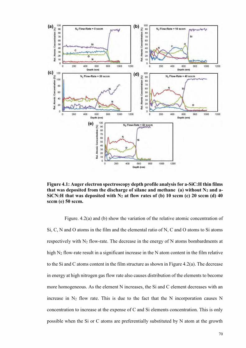
70
Figure 4.1: Auger electron spectroscopy depth profile analysis for a-SiC:H thin films that was deposited from the discharge of silane and methane (a) without N2 and a-SiCN:H that was deposited with N2 at flow rates of (b) 10 sccm (c) 20 sccm (d) 40 sccm (e) 50 sccm.
Figure. 4.2(a) and (b) show the variation of the relative atomic concentration of
Si, C, N and O atoms in the film and the elemental ratio of N, C and O atoms to Si atoms
respectively with N2 flow-rate. The decrease in the energy of N atoms bombardments at
high N2 flow-rate result in a significant increase in the N atom content in the film relative
to the Si and C atoms content in the film structure as shown in Figure 4.2(a). The decrease
in energy at high nitrogen gas flow rate also causes distribution of the elements to become
more homogeneous. As the element N increases, the Si and C element decreases with an
increase in N2 flow rate. This is due to the fact that the N incorporation causes N
concentration to increase at the expense of C and Si elements concentration. This is only
possible when the Si or C atoms are preferentially substituted by N atom at the growth
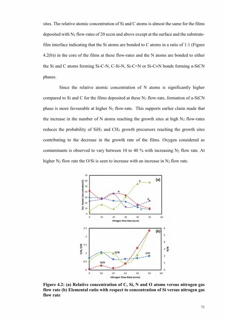
71
sites. The relative atomic concentration of Si and C atoms is almost the same for the films
deposited with N2 flow-rates of 20 sccm and above except at the surface and the substrate-
film interface indicating that the Si atoms are bonded to C atoms in a ratio of 1:1 (Figure
4.2(b)) in the core of the films at these flow-rates and the N atoms are bonded to either
the Si and C atoms forming Si-C-N, C-Si-N, Si-C=N or Si-CN bonds forming a-SiCN
phases.
Since the relative atomic concentration of N atoms is significantly higher
compared to Si and C for the films deposited at these N2 flow-rate, formation of a-SiCN
phase is more favourable at higher N2 flow-rate. This supports earlier claim made that
the increase in the number of N atoms reaching the growth sites at high N2 flow-rates
reduces the probability of SiH3 and CH3 growth precursors reaching the growth sites
contributing to the decrease in the growth rate of the films. Oxygen considered as
contaminants is observed to vary between 10 to 40 % with increasing N2 flow rate. At
higher N2 flow rate the O/Si is seen to increase with an increase in N2 flow rate.
Figure 4.2: (a) Relative concentration of C, Si, N and O atoms versus nitrogen gas flow rate (b) Elemental ratio with respect to concentration of Si versus nitrogen gas flow rate
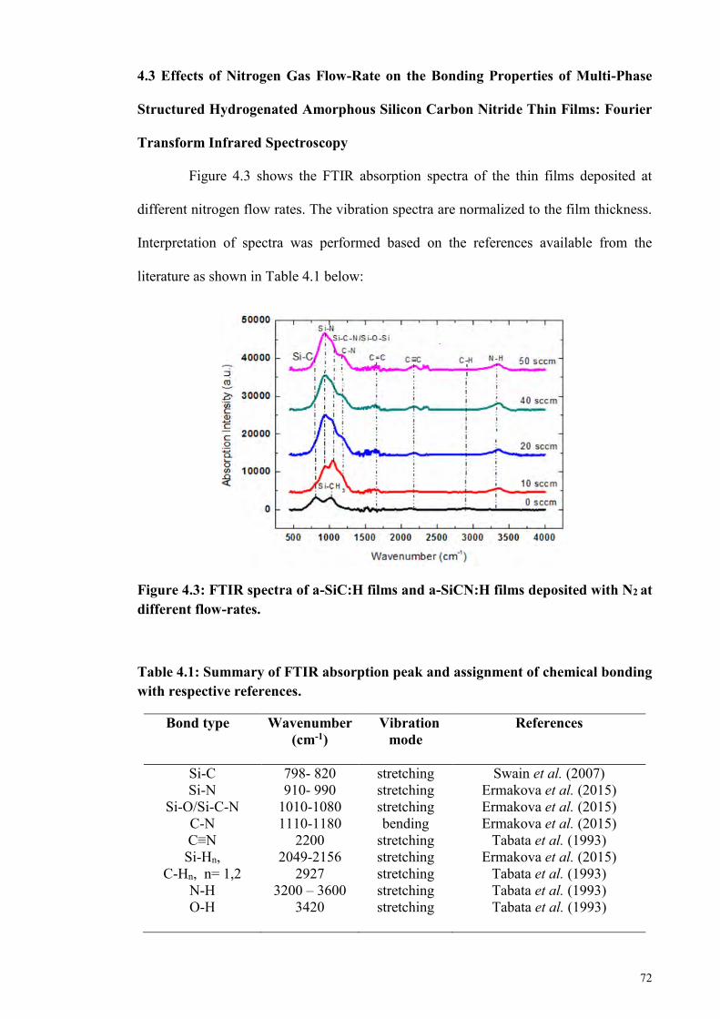
72
4.3 Effects of Nitrogen Gas Flow-Rate on the Bonding Properties of Multi-Phase
Structured Hydrogenated Amorphous Silicon Carbon Nitride Thin Films: Fourier
Transform Infrared Spectroscopy
Figure 4.3 shows the FTIR absorption spectra of the thin films deposited at
different nitrogen flow rates. The vibration spectra are normalized to the film thickness.
Interpretation of spectra was performed based on the references available from the
literature as shown in Table 4.1 below:
Figure 4.3: FTIR spectra of a-SiC:H films and a-SiCN:H films deposited with N2 at different flow-rates.
Table 4.1: Summary of FTIR absorption peak and assignment of chemical bonding with respective references.
Bond type Wavenumber (cm-1)
Vibration mode
References
Si-C Si-N
Si-O/Si-C-N C-N C≡N
Si-Hn, C-Hn, n= 1,2
N-H O-H
798- 820 910- 990
1010-1080 1110-1180
2200 2049-2156
2927 3200 – 3600
3420
stretching stretching stretching bending
stretching stretching stretching stretching stretching
Swain et al. (2007) Ermakova et al. (2015) Ermakova et al. (2015) Ermakova et al. (2015)
Tabata et al. (1993) Ermakova et al. (2015)
Tabata et al. (1993) Tabata et al. (1993) Tabata et al. (1993)
73
The a-SiC film shows strong bands at 813 cm-1 and 1009 cm-1 which correspond
to the Si-C and Si-CH3 wagging mode respectively (Swain & Dusane, 2007). In contrast
to the a-SiC, the FTIR absorption spectra for nitrogen incorporated films, the a-SiCN
films have more FTIR active regions. This is due to the fact that incorporation of nitrogen
has introduced more bonds species into the film structure and the assignment of some of
the absorptions peaks become more complicated.
Due to its high IR absorption, Region 1 (520 - 1300 cm-1) is the most important
band in the spectra, where the main vibration modes of the films molecular bond structure
should appear. The strong broad spectra band in Region 1 is featured in all as-prepared a-
SiCN films, exhibits overlapping absorption peaks of Si-C stretching mode at around
798 - 820 cm-1, Si-C-N/ Si-O at 1010-1080 cm-1, Si-N at 910 - 990 cm-1 and peaks in the
range between 1110 - 1180 cm-1 stretching bands are assigned to C-N wagging bonds
(Ermakova et al., 2015). Regarding the absorption band at 1010-1080 cm-1 and at 1100-
1180 cm-1 there are more than one view of the chemical bonds associated with those
vibrations. For the first vibration, some writers (Chu et al., 1995; Ermakova et al., 2015;
Kozak et al., 2015) relate this to the bond Si-O-Si stretching band but other few
researchers (Swain et al., 2014; Wu et al., 2002) opined that both Si-O and Si-C-N bond
causes the vibration.
In this work, it is strongly believed that these bands are attributed by Si-C-N
stretching instead of Si-O-Si stretching since the presence of N atoms is more dominant
than O atom by the AES data in Figure 4.1. For the second vibration band, Ermakova et
al. (2015) shows dominant presence of N atoms, this band is assigned to C-N band in this
work. Ermakova et al. (2015) reported the H-N or C-N bond responsible for the vibration
but another groups (Awad et al., 2010; Lu et al., 1998; Mihailescu et al., 1998) assigned
only C-N bond for the vibration. Again since the AES shows dominant presence of N
atoms, this band is assigned to C-N band in this work. The actual assignment of these
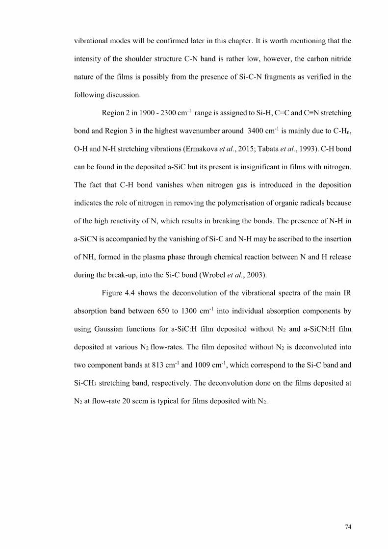
74
vibrational modes will be confirmed later in this chapter. It is worth mentioning that the
intensity of the shoulder structure C-N band is rather low, however, the carbon nitride
nature of the films is possibly from the presence of Si-C-N fragments as verified in the
following discussion.
Region 2 in 1900 - 2300 cm-1 range is assigned to Si-H, C=C and C≡N stretching
bond and Region 3 in the highest wavenumber around 3400 cm-1 is mainly due to C-Hn,
O-H and N-H stretching vibrations (Ermakova et al., 2015; Tabata et al., 1993). C-H bond
can be found in the deposited a-SiC but its present is insignificant in films with nitrogen.
The fact that C-H bond vanishes when nitrogen gas is introduced in the deposition
indicates the role of nitrogen in removing the polymerisation of organic radicals because
of the high reactivity of N, which results in breaking the bonds. The presence of N-H in
a-SiCN is accompanied by the vanishing of Si-C and N-H may be ascribed to the insertion
of NH, formed in the plasma phase through chemical reaction between N and H release
during the break-up, into the Si-C bond (Wrobel et al., 2003).
Figure 4.4 shows the deconvolution of the vibrational spectra of the main IR
absorption band between 650 to 1300 cm-1 into individual absorption components by
using Gaussian functions for a-SiC:H film deposited without N2 and a-SiCN:H film
deposited at various N2 flow-rates. The film deposited without N2 is deconvoluted into
two component bands at 813 cm-1 and 1009 cm-1, which correspond to the Si-C band and
Si-CH3 stretching band, respectively. The deconvolution done on the films deposited at
N2 at flow-rate 20 sccm is typical for films deposited with N2.
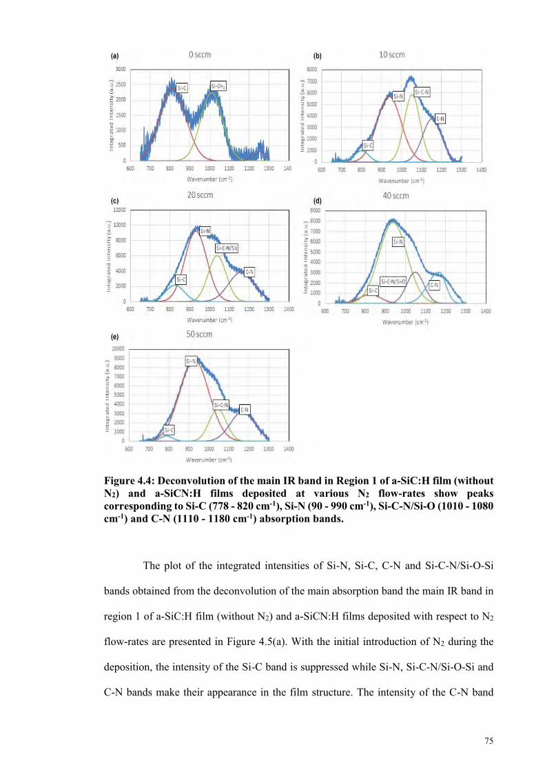
75
Figure 4.4: Deconvolution of the main IR band in Region 1 of a-SiC:H film (without N2) and a-SiCN:H films deposited at various N2 flow-rates show peaks corresponding to Si-C (778 - 820 cm-1), Si-N (90 - 990 cm-1), Si-C-N/Si-O (1010 - 1080 cm-1) and C-N (1110 - 1180 cm-1) absorption bands.
The plot of the integrated intensities of Si-N, Si-C, C-N and Si-C-N/Si-O-Si
bands obtained from the deconvolution of the main absorption band the main IR band in
region 1 of a-SiC:H film (without N2) and a-SiCN:H films deposited with respect to N2
flow-rates are presented in Figure 4.5(a). With the initial introduction of N2 during the
deposition, the intensity of the Si-C band is suppressed while Si-N, Si-C-N/Si-O-Si and
C-N bands make their appearance in the film structure. The intensity of the C-N band
76
decreases relative to the intensity of the Si-N band with the increase in N2 flow-rate. This
indicates the preference of N atoms to be bonded to Si atoms at higher N2 flow-rates. The
lower impact energy of the N atoms on reaching the growth sites makes it more favourable
for the N atoms to bond with Si compared to C atoms. Since the AES plots in Figure 4.2
shows that the relative concentration of Si and C atoms is the same at high N2 flow-rates,
the Si atoms therefore are mostly bonded to C≡N bonds to form Si-C≡N bonds and the
free Si bonds are free to be bonded to N atoms to form N rich a-SiCN phases in the film
structure.
Figure 4.5: Integrated intensity of (a) Si-N, C-N, Si-C and Si-C-N/Si-O-Si bonds and (b) N-H, C≡N and Si-H in as-deposited a-SiCN films versus nitrogen flow-rate.
77
The Si-C-N/Si-O-Si, C-N and Si-C band intensities show almost similar trends
with respect to N2 flow-rate. This strongly indicates that the Si-C and C-N bonds are
predominantly bonded together in the film structure forming the Si-C-N bonds. The AES
plots in Figure 4.2 show that at N2 flow-rates of 40 and 50 sccm, the relative atomic
concentration of N atoms is significantly higher as compared to Si, C or O. This strongly
suggests that the absorption band at 1010-1080 cm-1 represents Si-C-N bonds rather than
the Si-O-Si bonds in these films. The higher incorporation of N atoms into the film
structure promotes the formation of a-SiCN phases and removes O atoms contamination
in the film structure.
Figure 4.5(b) shows plot of the integrated intensities of N-H, C≡N and Si-H
bands versus N2 flow-rate. The intensity of N-H bonds increases significantly for the films
deposited at N2 flow-rates of 10 and 20 sccm and decreases when the N2 flow-rate is
increased to 40 and 50 sccm. The presence of C≡N bonds in the film structure increases
with increase in N2 flow-rate. At the higher N2 flow-rates, the formation of Si-H bonds is
more favourable suggesting higher incorporation of N atoms increases preference of H
and N atoms to bond with Si atoms. The increase in Si-N, C≡N and Si-H bonds with
increase in N2 flow-rate shows that formation of a-SiCN:H phases are more favourable
with increase in N2 flow-rate compared to a-SiCN phases. The N-H bonds are mostly
bonded to Si-H bonds and C≡N bonds are bonded to dangling bonds of Si atoms to form
a-SiCN:H phase in the film structure of these films. The film deposited at N2 flow-rate of
20 sccm shows significant presence of Si-C-N, Si-C, C-N and N-H bonds showing more
dominant presence of a-SiCN:H and a-SiC:H within the film structure compared to the
other films.
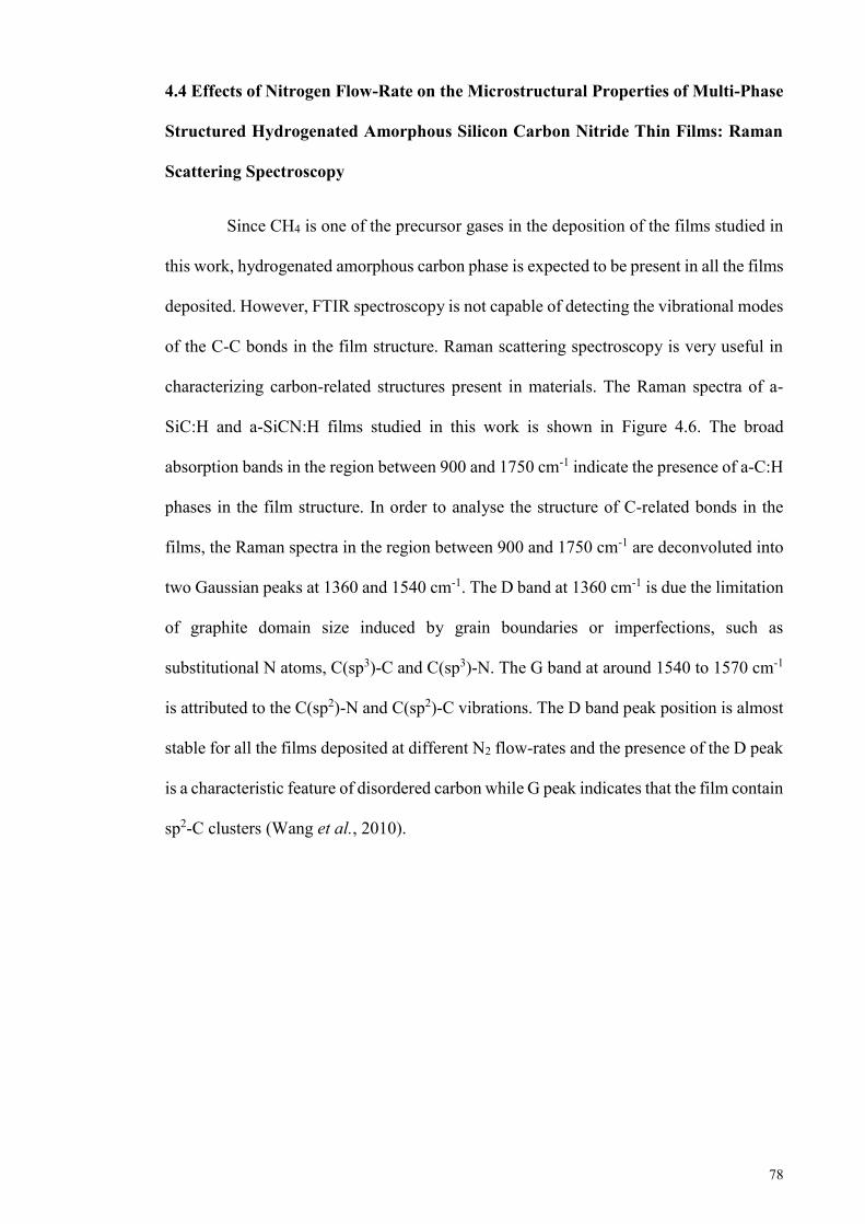
78
4.4 Effects of Nitrogen Flow-Rate on the Microstructural Properties of Multi-Phase
Structured Hydrogenated Amorphous Silicon Carbon Nitride Thin Films: Raman
Scattering Spectroscopy
Since CH4 is one of the precursor gases in the deposition of the films studied in
this work, hydrogenated amorphous carbon phase is expected to be present in all the films
deposited. However, FTIR spectroscopy is not capable of detecting the vibrational modes
of the C-C bonds in the film structure. Raman scattering spectroscopy is very useful in
characterizing carbon-related structures present in materials. The Raman spectra of a-
SiC:H and a-SiCN:H films studied in this work is shown in Figure 4.6. The broad
absorption bands in the region between 900 and 1750 cm-1 indicate the presence of a-C:H
phases in the film structure. In order to analyse the structure of C-related bonds in the
films, the Raman spectra in the region between 900 and 1750 cm-1 are deconvoluted into
two Gaussian peaks at 1360 and 1540 cm-1. The D band at 1360 cm-1 is due the limitation
of graphite domain size induced by grain boundaries or imperfections, such as
substitutional N atoms, C(sp3)-C and C(sp3)-N. The G band at around 1540 to 1570 cm-1
is attributed to the C(sp2)-N and C(sp2)-C vibrations. The D band peak position is almost
stable for all the films deposited at different N2 flow-rates and the presence of the D peak
is a characteristic feature of disordered carbon while G peak indicates that the film contain
sp2-C clusters (Wang et al., 2010).
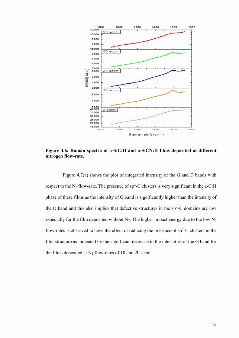
79
Figure 4.6: Raman spectra of a-SiC:H and a-SiCN:H films deposited at different nitrogen flow-rate.
Figure 4.7(a) shows the plot of integrated intensity of the G and D bands with
respect to the N2 flow-rate. The presence of sp2-C clusters is very significant in the a-C:H
phase of these films as the intensity of G band is significantly higher than the intensity of
the D band and this also implies that defective structures in the sp2-C domains are low
especially for the film deposited without N2. The higher impact energy due to the low N2
flow-rates is observed to have the effect of reducing the presence of sp2-C clusters in the
film structure as indicated by the significant decrease in the intensities of the G band for
the films deposited at N2 flow-rates of 10 and 20 sccm.
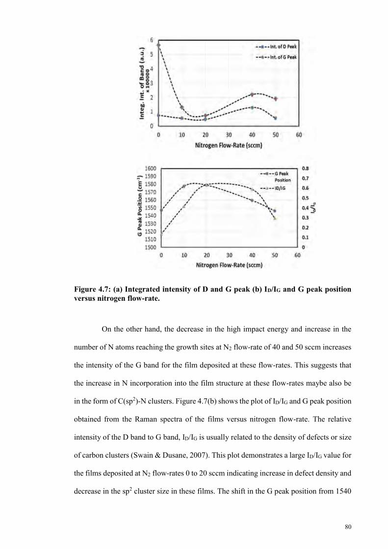
80
Figure 4.7: (a) Integrated intensity of D and G peak (b) ID/IG and G peak position versus nitrogen flow-rate.
On the other hand, the decrease in the high impact energy and increase in the
number of N atoms reaching the growth sites at N2 flow-rate of 40 and 50 sccm increases
the intensity of the G band for the film deposited at these flow-rates. This suggests that
the increase in N incorporation into the film structure at these flow-rates maybe also be
in the form of C(sp2)-N clusters. Figure 4.7(b) shows the plot of ID/IG and G peak position
obtained from the Raman spectra of the films versus nitrogen flow-rate. The relative
intensity of the D band to G band, ID/IG is usually related to the density of defects or size
of carbon clusters (Swain & Dusane, 2007). This plot demonstrates a large ID/IG value for
the films deposited at N2 flow-rates 0 to 20 sccm indicating increase in defect density and
decrease in the sp2 cluster size in these films. The shift in the G peak position from 1540
81
to 1580 cm-1 for the films deposited at low N2 flow-rates of 10 and 20 sccm shows
increase in residual compressive stress on the films confirming that impact energy of the
N atoms impinging on the growth sites is higher at these flow-rates. The film deposited
at N2 flow-rate of 40-50 sccm show a significant decrease in the ID/IG and G peak position
suggesting that the decrease in impact energy and increase in the number of reactive N
atoms at the growth sites reduce residual compressive stress on the sp2-C clusters resulting
in increase in the size of the sp2-C clusters.
4.5 Effects of Nitrogen Flow-Rate on the Deposition Rate of Multi-Phase Structured
Amorphous Silicon Carbon Nitride Thin Films
The deposition rate of hydrogenated amorphous silicon carbide (a-SiC:H) and
hydrogenated amorphous silicon carbon nitride (a-SiCN:H) thin films that were deposited
on both c-Si and glass substrates versus N2 flow-rate is shown in Figure 4.8. The films on
c-Si show higher growth rates and the variation with N2 flow rate is similar for films on
both c-Si and glass substrates. The similar trends of growth rates with respect to N2 flow-
rate for the films grown on c-Si and glass substrates show that the presence of O atoms
within the film structure does not have significant effect on the film growth rates since
glass substrates are practically free of O atoms unlike c-Si substrates, which are easily
oxidized prior to deposition even when placed in a highly evacuated growth chamber.
As mentioned earlier, increase in N2 flow-rate increases the number of reactive N
atoms with lower energy reaching the growth sites. The impact energy of these atoms
decreases with increase in N2 flow-rate due higher frequency in collisions with the
increasing number of N2 molecules along with the presence of SiH4 and CH4 molecules
in the plasma. The increase in the number of N atoms reaching the growth sites reduces
the probability of SiH3 and CH3 growth precursors reaching the growth sites, which
contributes to the decrease in the growth rate of the films with increase in N2 flow-rate.
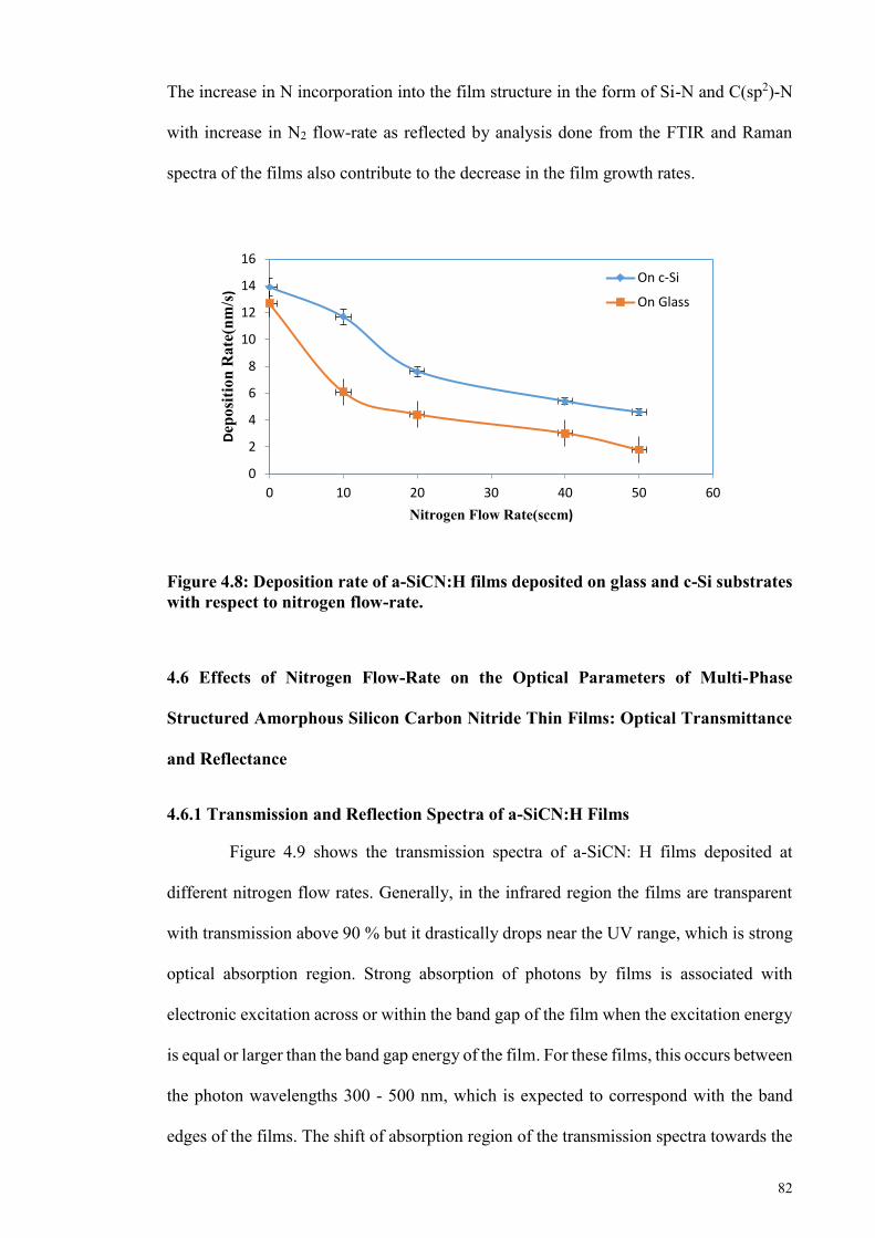
82
The increase in N incorporation into the film structure in the form of Si-N and C(sp2)-N
with increase in N2 flow-rate as reflected by analysis done from the FTIR and Raman
spectra of the films also contribute to the decrease in the film growth rates.
Figure 4.8: Deposition rate of a-SiCN:H films deposited on glass and c-Si substrates with respect to nitrogen flow-rate.
4.6 Effects of Nitrogen Flow-Rate on the Optical Parameters of Multi-Phase
Structured Amorphous Silicon Carbon Nitride Thin Films: Optical Transmittance
and Reflectance
4.6.1 Transmission and Reflection Spectra of a-SiCN:H Films
Figure 4.9 shows the transmission spectra of a-SiCN: H films deposited at
different nitrogen flow rates. Generally, in the infrared region the films are transparent
with transmission above 90 % but it drastically drops near the UV range, which is strong
optical absorption region. Strong absorption of photons by films is associated with
electronic excitation across or within the band gap of the film when the excitation energy
is equal or larger than the band gap energy of the film. For these films, this occurs between
the photon wavelengths 300 - 500 nm, which is expected to correspond with the band
edges of the films. The shift of absorption region of the transmission spectra towards the
0
2
4
6
8
10
12
14
16
0 10 20 30 40 50 60
Dep
ositi
on R
ate(
nm/s
)
Nitrogen Flow Rate(sccm)
On c-Si
On Glass
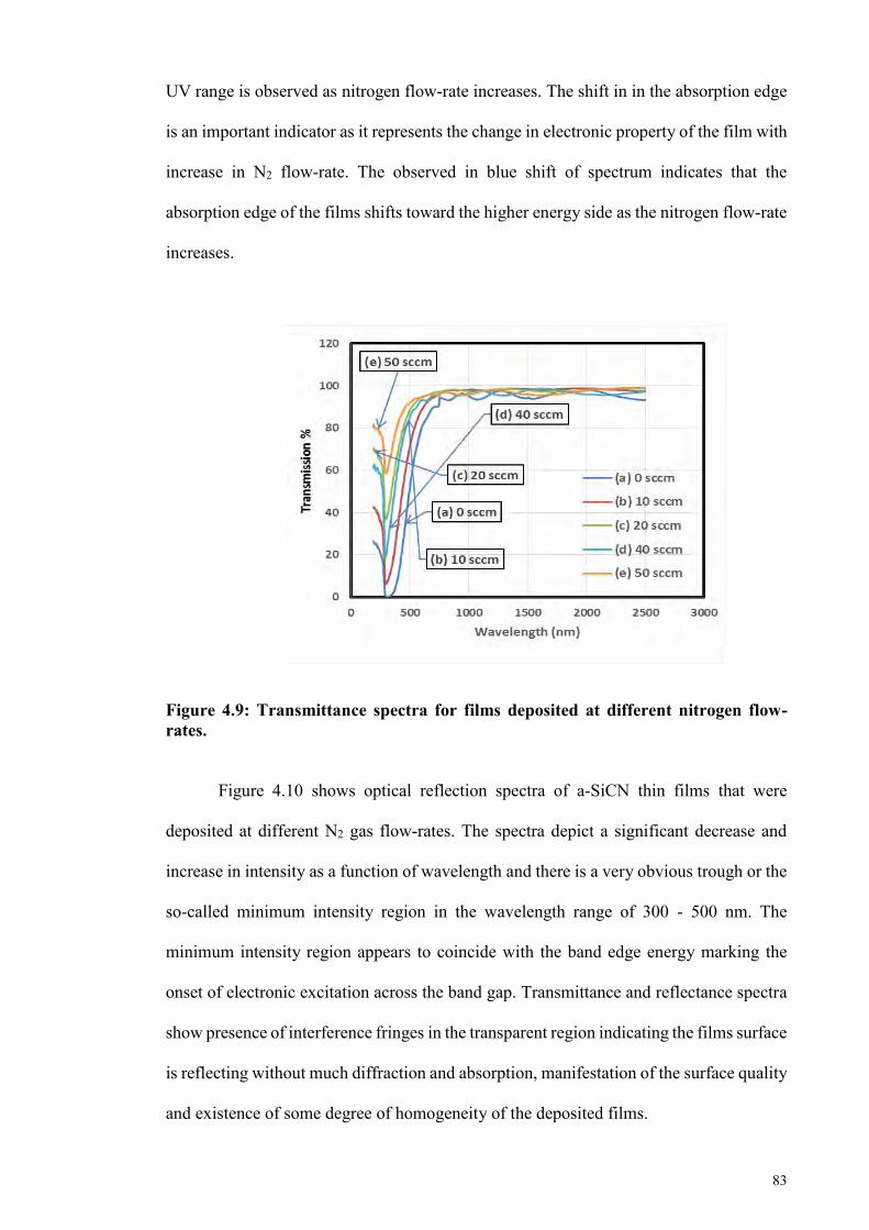
83
UV range is observed as nitrogen flow-rate increases. The shift in in the absorption edge
is an important indicator as it represents the change in electronic property of the film with
increase in N2 flow-rate. The observed in blue shift of spectrum indicates that the
absorption edge of the films shifts toward the higher energy side as the nitrogen flow-rate
increases.
Figure 4.9: Transmittance spectra for films deposited at different nitrogen flow-rates.
Figure 4.10 shows optical reflection spectra of a-SiCN thin films that were
deposited at different N2 gas flow-rates. The spectra depict a significant decrease and
increase in intensity as a function of wavelength and there is a very obvious trough or the
so-called minimum intensity region in the wavelength range of 300 - 500 nm. The
minimum intensity region appears to coincide with the band edge energy marking the
onset of electronic excitation across the band gap. Transmittance and reflectance spectra
show presence of interference fringes in the transparent region indicating the films surface
is reflecting without much diffraction and absorption, manifestation of the surface quality
and existence of some degree of homogeneity of the deposited films.
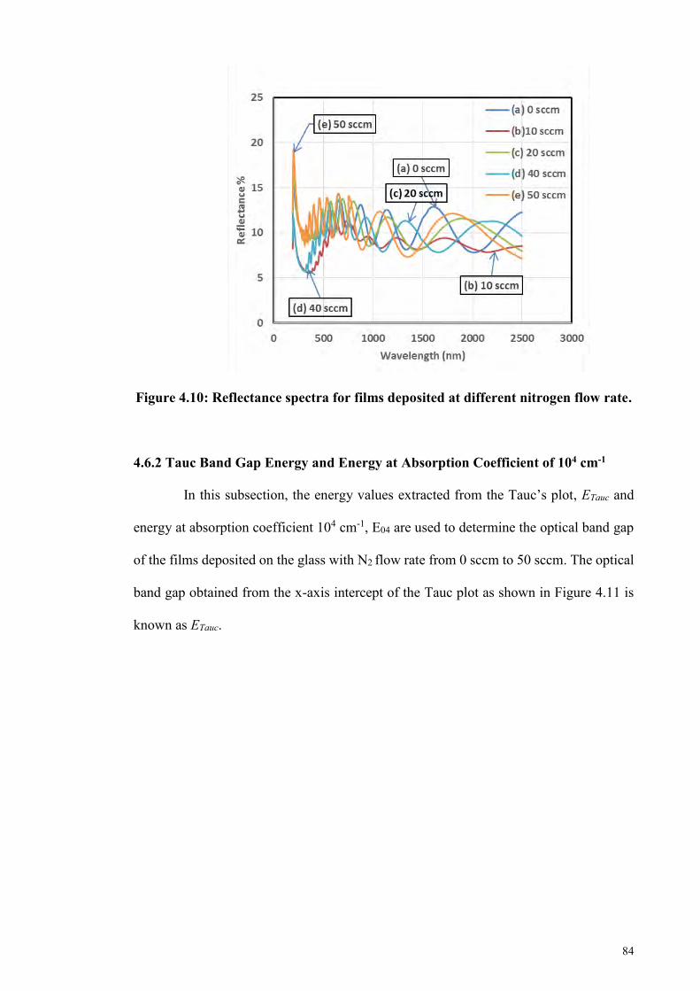
84
Figure 4.10: Reflectance spectra for films deposited at different nitrogen flow rate.
4.6.2 Tauc Band Gap Energy and Energy at Absorption Coefficient of 104 cm-1
In this subsection, the energy values extracted from the Tauc’s plot, ETauc and
energy at absorption coefficient 104 cm-1, E04 are used to determine the optical band gap
of the films deposited on the glass with N2 flow rate from 0 sccm to 50 sccm. The optical
band gap obtained from the x-axis intercept of the Tauc plot as shown in Figure 4.11 is
known as ETauc.
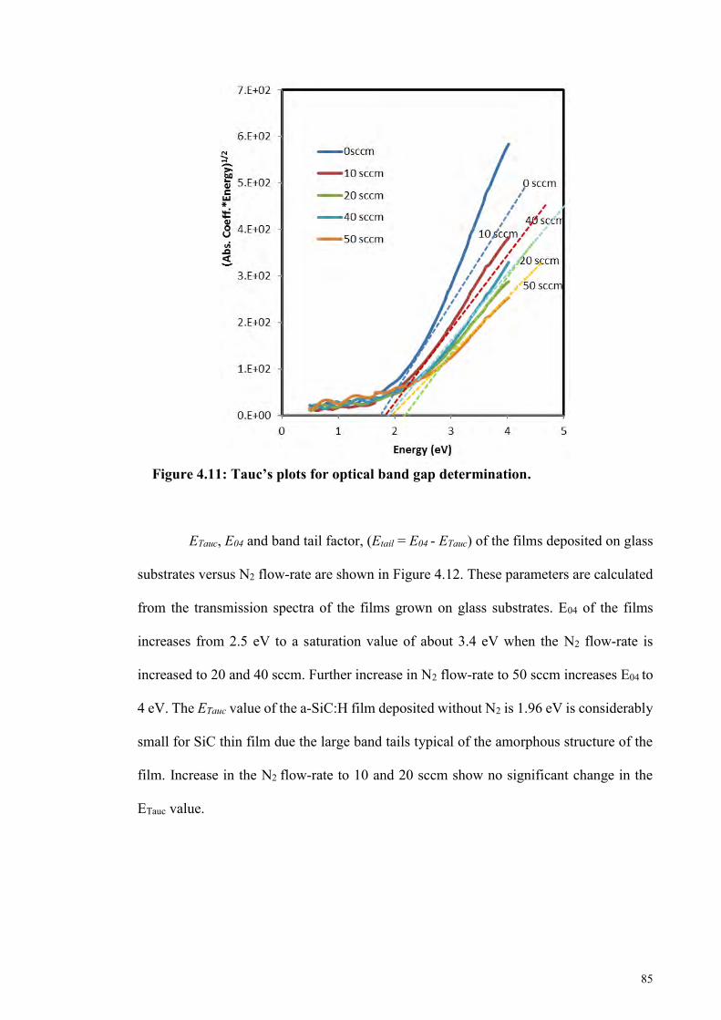
85
Figure 4.11: Tauc’s plots for optical band gap determination.
ETauc, E04 and band tail factor, (Etail = E04 - ETauc) of the films deposited on glass
substrates versus N2 flow-rate are shown in Figure 4.12. These parameters are calculated
from the transmission spectra of the films grown on glass substrates. E04 of the films
increases from 2.5 eV to a saturation value of about 3.4 eV when the N2 flow-rate is
increased to 20 and 40 sccm. Further increase in N2 flow-rate to 50 sccm increases E04 to
4 eV. The ETauc value of the a-SiC:H film deposited without N2 is 1.96 eV is considerably
small for SiC thin film due the large band tails typical of the amorphous structure of the
film. Increase in the N2 flow-rate to 10 and 20 sccm show no significant change in the
ETauc value.
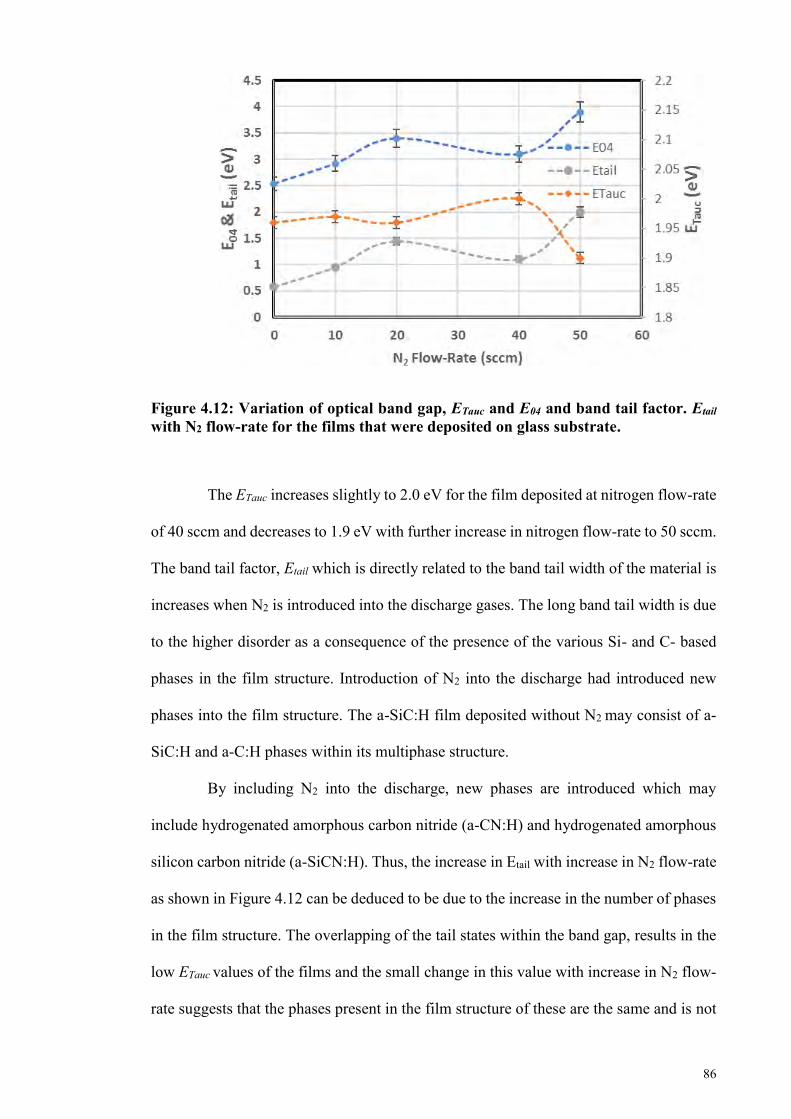
86
Figure 4.12: Variation of optical band gap, ETauc and E04 and band tail factor. Etail with N2 flow-rate for the films that were deposited on glass substrate.
The ETauc increases slightly to 2.0 eV for the film deposited at nitrogen flow-rate
of 40 sccm and decreases to 1.9 eV with further increase in nitrogen flow-rate to 50 sccm.
The band tail factor, Etail which is directly related to the band tail width of the material is
increases when N2 is introduced into the discharge gases. The long band tail width is due
to the higher disorder as a consequence of the presence of the various Si- and C- based
phases in the film structure. Introduction of N2 into the discharge had introduced new
phases into the film structure. The a-SiC:H film deposited without N2 may consist of a-
SiC:H and a-C:H phases within its multiphase structure.
By including N2 into the discharge, new phases are introduced which may
include hydrogenated amorphous carbon nitride (a-CN:H) and hydrogenated amorphous
silicon carbon nitride (a-SiCN:H). Thus, the increase in Etail with increase in N2 flow-rate
as shown in Figure 4.12 can be deduced to be due to the increase in the number of phases
in the film structure. The overlapping of the tail states within the band gap, results in the
low ETauc values of the films and the small change in this value with increase in N2 flow-
rate suggests that the phases present in the film structure of these are the same and is not
87
dependent on the N2 flow-rate. The N2 flow-rate produces significant effects on the E04
and Etail values which are dependent on the dominant phase present in the film structure.
4.6.3 Refractive Index
Figure 4.13 shows the dispersion curves for the refractive indices of a-SiC:H
films and a-SiCN:H that are deposited at different N2 flow-rates. The refractive index
dispersion curve of a-SiC:H film is higher than the refractive index curves of a-SiCN:H
films deposited at various N2 flow-rates. In general, the refractive index of each film is
high in the lower wavelength region, which is consistent with the normal dispersion
behaviour of refractive index of most materials. At higher wavelength (in the infrared)
the refractive index saturates to a constant or static values (between 1.55 – 1.70),
indicating the films become non-dispersive at this region.
It is very clear that the index becomes smaller as nitrogen gas is introduced into
the films. There is an indication from the AES in Figure 4.2 that N atom concentration
increases with increasing nitrogen-flow rate whereas C atom concentration drops when
N atoms are present in the film. From these results, the decrease in refractive index can
be attributed mainly to the formation of Si-N bonds in the film structure. Also, it is
observed that the significant decrease in the intensity of the Raman spectra and the G
peak in Figure 4.6 for the films deposited with N2 indicates carbon phase, a-C:H decreases
soon as nitrogen is introduced into the films. The reduction in carbon phase makes the
film becomes less dense and causes the lower refractive index to be obtained
(Chattopadhyay et al., 2001).
High refractive index is related to the films of high absorption, therefore a drop
in refractive index means the incorporation of nitrogen gas causes less absorption by the
films, which means the films have better transparency to the incidence light especially in
the region of absorption edges. This is in agreement with the earlier result where the
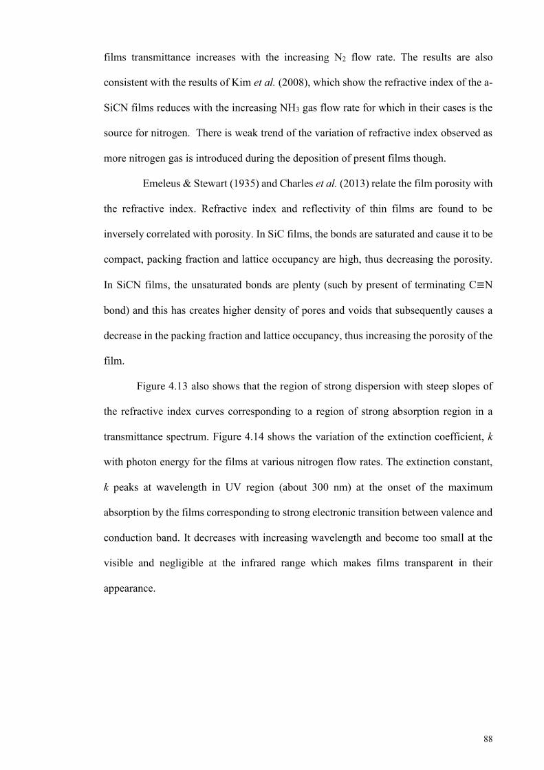
88
films transmittance increases with the increasing N2 flow rate. The results are also
consistent with the results of Kim et al. (2008), which show the refractive index of the a-
SiCN films reduces with the increasing NH3 gas flow rate for which in their cases is the
source for nitrogen. There is weak trend of the variation of refractive index observed as
more nitrogen gas is introduced during the deposition of present films though.
Emeleus & Stewart (1935) and Charles et al. (2013) relate the film porosity with
the refractive index. Refractive index and reflectivity of thin films are found to be
inversely correlated with porosity. In SiC films, the bonds are saturated and cause it to be
compact, packing fraction and lattice occupancy are high, thus decreasing the porosity.
In SiCN films, the unsaturated bonds are plenty (such by present of terminating C≡N
bond) and this has creates higher density of pores and voids that subsequently causes a
decrease in the packing fraction and lattice occupancy, thus increasing the porosity of the
film.
Figure 4.13 also shows that the region of strong dispersion with steep slopes of
the refractive index curves corresponding to a region of strong absorption region in a
transmittance spectrum. Figure 4.14 shows the variation of the extinction coefficient, k
with photon energy for the films at various nitrogen flow rates. The extinction constant,
k peaks at wavelength in UV region (about 300 nm) at the onset of the maximum
absorption by the films corresponding to strong electronic transition between valence and
conduction band. It decreases with increasing wavelength and become too small at the
visible and negligible at the infrared range which makes films transparent in their
appearance.
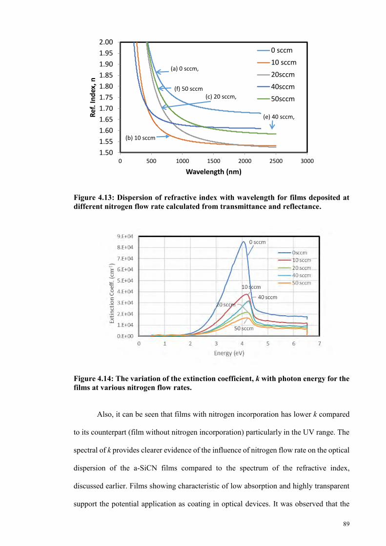
89
Figure 4.13: Dispersion of refractive index with wavelength for films deposited at different nitrogen flow rate calculated from transmittance and reflectance.
Figure 4.14: The variation of the extinction coefficient, k with photon energy for the films at various nitrogen flow rates.
Also, it can be seen that films with nitrogen incorporation has lower k compared
to its counterpart (film without nitrogen incorporation) particularly in the UV range. The
spectral of k provides clearer evidence of the influence of nitrogen flow rate on the optical
dispersion of the a-SiCN films compared to the spectrum of the refractive index,
discussed earlier. Films showing characteristic of low absorption and highly transparent
support the potential application as coating in optical devices. It was observed that the
(a) 0 sccm,
(b) 10 sccm
(c) 20 sccm,
(e) 40 sccm,
(f) 50 sccm
1.50
1.55
1.60
1.65
1.70
1.75
1.80
1.85
1.90
1.95
2.00
0 500 1000 1500 2000 2500 3000
Ref
. In
dex
, n
Wavelength (nm)
0 sccm
10 sccm
20sccm
40sccm
50sccm
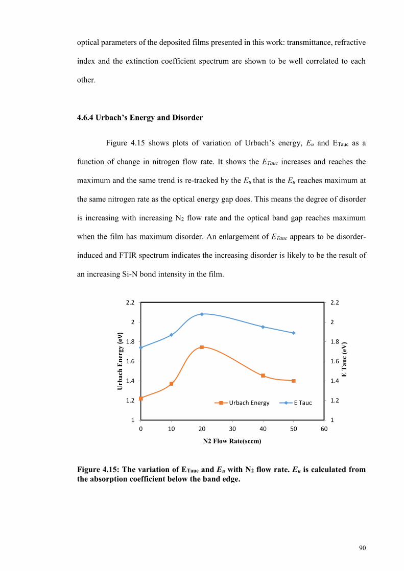
90
optical parameters of the deposited films presented in this work: transmittance, refractive
index and the extinction coefficient spectrum are shown to be well correlated to each
other.
4.6.4 Urbach’s Energy and Disorder
Figure 4.15 shows plots of variation of Urbach’s energy, Eu and ETauc as a
function of change in nitrogen flow rate. It shows the ETauc increases and reaches the
maximum and the same trend is re-tracked by the Eu that is the Eu reaches maximum at
the same nitrogen rate as the optical energy gap does. This means the degree of disorder
is increasing with increasing N2 flow rate and the optical band gap reaches maximum
when the film has maximum disorder. An enlargement of ETauc appears to be disorder-
induced and FTIR spectrum indicates the increasing disorder is likely to be the result of
an increasing Si-N bond intensity in the film.
Figure 4.15: The variation of ETauc and Eu with N2 flow rate. Eu is calculated from the absorption coefficient below the band edge.
1
1.2
1.4
1.6
1.8
2
2.2
1
1.2
1.4
1.6
1.8
2
2.2
0 10 20 30 40 50 60
E T
auc
(eV
)
Urb
ach
Ene
rgy
(eV
)
N2 Flow Rate(sccm)
Urbach Energy E Tauc
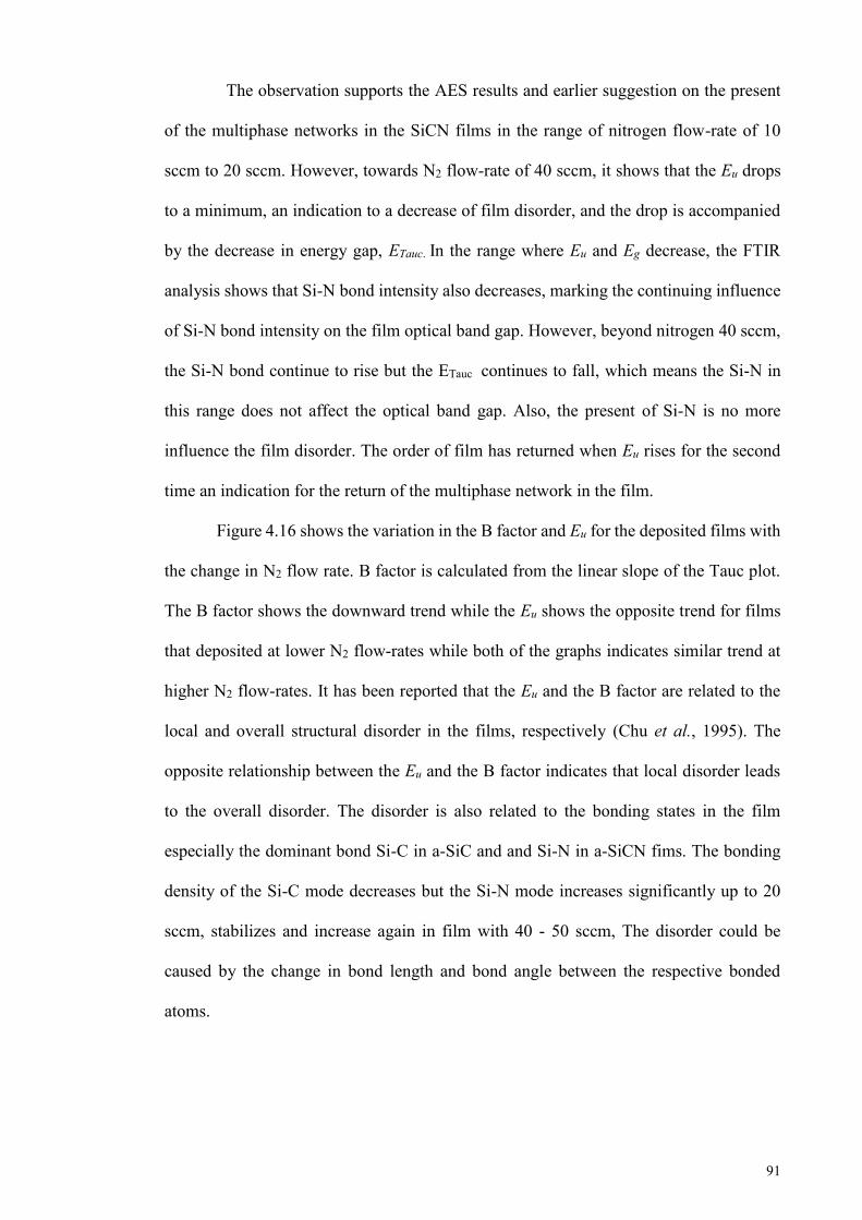
91
The observation supports the AES results and earlier suggestion on the present
of the multiphase networks in the SiCN films in the range of nitrogen flow-rate of 10
sccm to 20 sccm. However, towards N2 flow-rate of 40 sccm, it shows that the Eu drops
to a minimum, an indication to a decrease of film disorder, and the drop is accompanied
by the decrease in energy gap, ETauc. In the range where Eu and Eg decrease, the FTIR
analysis shows that Si-N bond intensity also decreases, marking the continuing influence
of Si-N bond intensity on the film optical band gap. However, beyond nitrogen 40 sccm,
the Si-N bond continue to rise but the ETauc continues to fall, which means the Si-N in
this range does not affect the optical band gap. Also, the present of Si-N is no more
influence the film disorder. The order of film has returned when Eu rises for the second
time an indication for the return of the multiphase network in the film.
Figure 4.16 shows the variation in the B factor and Eu for the deposited films with
the change in N2 flow rate. B factor is calculated from the linear slope of the Tauc plot.
The B factor shows the downward trend while the Eu shows the opposite trend for films
that deposited at lower N2 flow-rates while both of the graphs indicates similar trend at
higher N2 flow-rates. It has been reported that the Eu and the B factor are related to the
local and overall structural disorder in the films, respectively (Chu et al., 1995). The
opposite relationship between the Eu and the B factor indicates that local disorder leads
to the overall disorder. The disorder is also related to the bonding states in the film
especially the dominant bond Si-C in a-SiC and and Si-N in a-SiCN fims. The bonding
density of the Si-C mode decreases but the Si-N mode increases significantly up to 20
sccm, stabilizes and increase again in film with 40 - 50 sccm, The disorder could be
caused by the change in bond length and bond angle between the respective bonded
atoms.
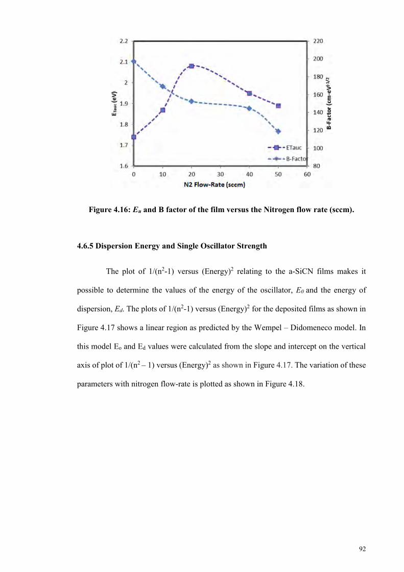
92
Figure 4.16: Eu and B factor of the film versus the Nitrogen flow rate (sccm).
4.6.5 Dispersion Energy and Single Oscillator Strength
The plot of 1/(n2-1) versus (Energy)2 relating to the a-SiCN films makes it
possible to determine the values of the energy of the oscillator, E0 and the energy of
dispersion, Ed. The plots of 1/(n2-1) versus (Energy)2 for the deposited films as shown in
Figure 4.17 shows a linear region as predicted by the Wempel – Didomeneco model. In
this model Eo and Ed values were calculated from the slope and intercept on the vertical
axis of plot of 1/(n2 – 1) versus (Energy)2 as shown in Figure 4.17. The variation of these
parameters with nitrogen flow-rate is plotted as shown in Figure 4.18.
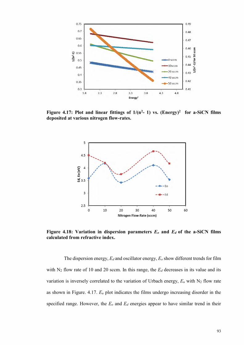
93
Figure 4.17: Plot and linear fittings of 1/(n2- 1) vs. (Energy)2 for a-SiCN films deposited at various nitrogen flow-rates.
Figure 4.18: Variation in dispersion parameters Eo and Ed of the a-SiCN films calculated from refractive index.
The dispersion energy, Ed and oscillator energy, Eo show different trends for film
with N2 flow rate of 10 and 20 sccm. In this range, the Ed decreases in its value and its
variation is inversely correlated to the variation of Urbach energy, Eu with N2 flow rate
as shown in Figure. 4.17. Eu plot indicates the films undergo increasing disorder in the
specified range. However, the Eo and Ed energies appear to have similar trend in their
94
variation with nitrogen flow rate above the flow rate 20 sccm which corresponds to a
range of decreasing disorder in Eu term.
4.7 Origin of Photoluminescence in Multi-Phase Structured Hydrogenated
Amorphous Silicon Carbide and Silicon Carbon Nitride thin films.
The origin of PL in the multi-phase structured a-SiC:H and a-SiCN:H films
deposited at different N2 flow-rates are investigated by studying the behaviour of PL
emission properties of these films deposited on c-Si and glass substrates. The PL emission
properties investigated are the PL emission peak position and PL emission intensity.
These PL properties will be related to the compositional, microstructure and optical
properties of the films to hypothesize the origin of PL emission in these films.
4.7.1 Effects of Nitrogen Flow-Rate on the Photoluminescence Properties of Films
Deposited on c-Si Substrates
Figure. 4.19(a) to (e) shows the PL spectra of the a-SiC:H and a-SiCN:H films
deposited without N2 and at N2 flow-rate of 10 sccm to 50 sccm respectively on c-Si
substrates. The spectra are deconvoluted into the component peaks contributing to the
main spectra. The broad PL emission peaks covering spectral range from 400 to 750 nm
indicate the multi-phase structure of the films and emission spectra are due to overlapping
emission band spectra produced by the different phases in the film structure.
95
Figure. 4.19: Deconvoluted PL emission spectra of a-SiC:H and a-SiCN:H thin films deposited on c-Si deposited with N2 flow-rate of (a) 0, (b) 10, (c) 20, (d) 40 and (e) 50 sccm.
The integrated intensity and peak positions of the deconvoluted peaks are
analysed to determine the origin of the PL emission in these films. Figure 4.20(a) and (b)
show the peak position and emission intensity respectively of the various component
peaks obtained from the deconvolution of the PL emission spectra of the films deposited
on c-Si substrates. For the a-SiC:H film deposited from the discharge of SiH4 and CH4
without N2, deconvolution of the PL spectrum results in one dominant peak labelled as
Pk 4 at 2.13 eV and three low intensity PL peaks at 2.81, 2.41 and 1.85 eV labelled as
Pk1, Pk2 and Pk5 respectively as shown in Figure 4.20 (b). Pk3 band (2.3 eV) is found
only in films with N2.
The PL emission is significantly high for the a-SiC:H film compared to the a-
SiCN:H films deposited with N2. Tabata et al. (2004) proposed that the origin of PL
96
emission from their a-SiC:H films at 2.21 eV occurs through recombination within tail
states of a-C:H in their films where the tail states are formed from sp2-C clusters in the
film. Since the a-SiCN:H film is multi-phase in structure, it can be deduced that the
intense PL emission from this film is of similar origin with the peak red-shifted to 2.13
eV. This component of PL emission (Pk4) is significantly suppressed for the films
deposited with N2. The significant decrease in the intensity of the Raman spectra and the
G peak in Figure 4.7(a) for the films deposited with N2 support that the origin of this PL
emission is from the a-C:H phase in the film structure. The N2 discharge during the
deposition process has results in the incorporation of N within the film structure in the
form of Si-N, C-N and N-H bonds.
Figure 4.20: (a) Peak positions and (b) PL emission intensities of the deconvoluted peaks obtained from the PL emission spectra of the films on c-Si substrates versus nitrogen flow-rate.
97
Wu et al. (2014) attributed the peak at 416 nm (2.96 eV) in their SiCN films
to the defects in a region where the carbon clusters are surrounded by Si-C matrix. It is
suggested the weak PL emission peak, Pk1 at 2.81 eV (441 nm) may be contributed by
the Si-C matrix from the a-SiC:H phase surrounding the carbon clusters in the film
deposited without N2. Figure 4.20(b) and 4.5(b) show that the trend of the PL emission
intensity of Pk1 and the integrated intensity of the Si-C band are almost similar and this
has supported the as-proposed origin of the PL emission. Incorporation of N into the film
structure also results in the emergence of Pk3 at 2.3 eV. Pk2 at 2.41 eV shows similar
trend with N2 flow-rate as Pk3. Since Pk3 is present only in the films deposited with N2,
the origin of this PL emission is proposed to be from the recombination within tail states
of a-CN:H and a-SiCN:H phases in the film structure where the tail states are formed
from C(sp2)-N clusters instead of C(sp2)-C clusters in the film.
The integrated intensities of the C-N and Si-C-N bands in suppure 4(a) show
similar trends with N2 flow-rate as the PL emission intensity of Pk3 and Pk2. Thus, PL
emission from Pk2 and Pk3 may have their origin in the a-CN:H and a-SiCN:H phase in
the film structure due to radiative recombination in the tail states of the C(sp2)-N clusters.
The low intensity PL emission of Pk2 is probably due to the lower sp2 cluster size
involved. The lower energy of Pk3 is probably due to emission from the phase with higher
defects resulting in longer tail states and the a-SiCN:H phase having more elements
involved may result in higher defect density. Thus, it can be concluded that the origin of
PL emission produced by Pk3 and Pk2 is due to recombination in the tail states of the
C(sp2)-N clusters in the a-SiCN:H and a-CN:H phases respectively. Pk5 is the lowest
energy PL emission with emission intensity higher than PL emission of Pk2. This PL
emission may have its origin from radiative recombination in the tail states of H related
bonds in the film structure formed from N-H or Si-H bonds.
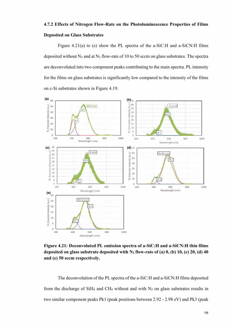
98
4.7.2 Effects of Nitrogen Flow-Rate on the Photoluminescence Properties of Films
Deposited on Glass Substrates
Figure 4.21(a) to (e) show the PL spectra of the a-SiC:H and a-SiCN:H films
deposited without N2 and at N2 flow-rate of 10 to 50 sccm on glass substrates. The spectra
are deconvoluted into two component peaks contributing to the main spectra. PL intensity
for the films on glass substrates is significantly low compared to the intensity of the films
on c-Si substrates shown in Figure 4.19.
Figure 4.21: Deconvoluted PL emission spectra of a-SiC:H and a-SiCN:H thin films deposited on glass substrate deposited with N2 flow-rate of (a) 0, (b) 10, (c) 20, (d) 40 and (e) 50 sccm respectively.
The deconvolution of the PL spectra of the a-SiC:H and a-SiCN:H films deposited
from the discharge of SiH4 and CH4 without and with N2 on glass substrates results in
two similar component peaks Pk1 (peak positions between 2.92 - 2.98 eV) and Pk3 (peak
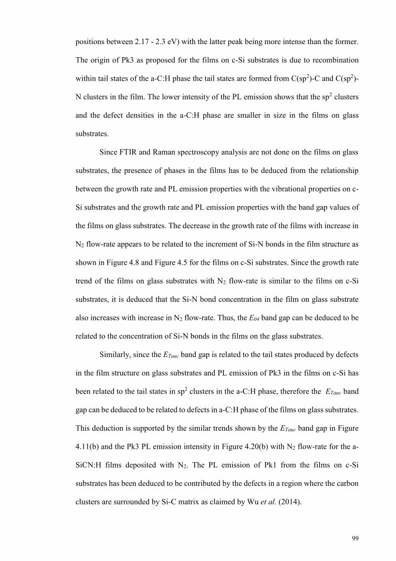
99
positions between 2.17 - 2.3 eV) with the latter peak being more intense than the former.
The origin of Pk3 as proposed for the films on c-Si substrates is due to recombination
within tail states of the a-C:H phase the tail states are formed from C(sp2)-C and C(sp2)-
N clusters in the film. The lower intensity of the PL emission shows that the sp2 clusters
and the defect densities in the a-C:H phase are smaller in size in the films on glass
substrates.
Since FTIR and Raman spectroscopy analysis are not done on the films on glass
substrates, the presence of phases in the films has to be deduced from the relationship
between the growth rate and PL emission properties with the vibrational properties on c-
Si substrates and the growth rate and PL emission properties with the band gap values of
the films on glass substrates. The decrease in the growth rate of the films with increase in
N2 flow-rate appears to be related to the increment of Si-N bonds in the film structure as
shown in Figure 4.8 and Figure 4.5 for the films on c-Si substrates. Since the growth rate
trend of the films on glass substrates with N2 flow-rate is similar to the films on c-Si
substrates, it is deduced that the Si-N bond concentration in the film on glass substrate
also increases with increase in N2 flow-rate. Thus, the E04 band gap can be deduced to be
related to the concentration of Si-N bonds in the films on the glass substrates.
Similarly, since the ETauc band gap is related to the tail states produced by defects
in the film structure on glass substrates and PL emission of Pk3 in the films on c-Si has
been related to the tail states in sp2 clusters in the a-C:H phase, therefore the ETauc band
gap can be deduced to be related to defects in a-C:H phase of the films on glass substrates.
This deduction is supported by the similar trends shown by the ETauc band gap in Figure
4.11(b) and the Pk3 PL emission intensity in Figure 4.20(b) with N2 flow-rate for the a-
SiCN:H films deposited with N2. The PL emission of Pk1 from the films on c-Si
substrates has been deduced to be contributed by the defects in a region where the carbon
clusters are surrounded by Si-C matrix as claimed by Wu et al. (2014).
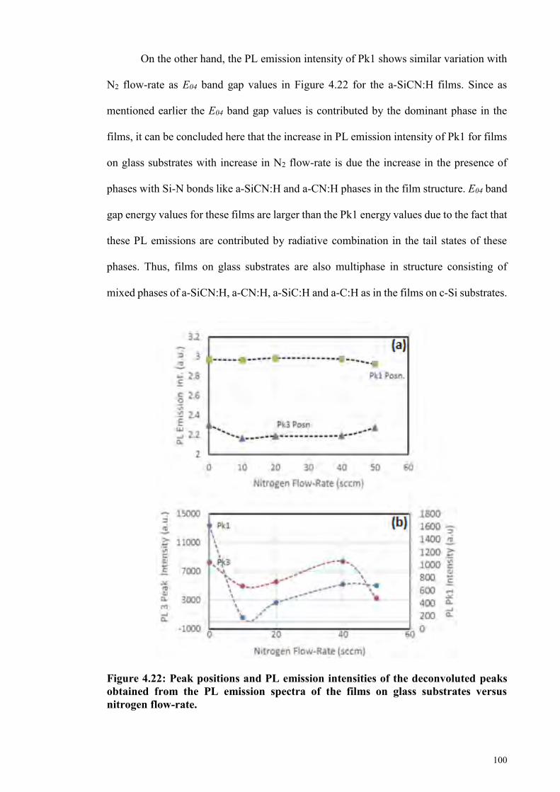
100
On the other hand, the PL emission intensity of Pk1 shows similar variation with
N2 flow-rate as E04 band gap values in Figure 4.22 for the a-SiCN:H films. Since as
mentioned earlier the E04 band gap values is contributed by the dominant phase in the
films, it can be concluded here that the increase in PL emission intensity of Pk1 for films
on glass substrates with increase in N2 flow-rate is due the increase in the presence of
phases with Si-N bonds like a-SiCN:H and a-CN:H phases in the film structure. E04 band
gap energy values for these films are larger than the Pk1 energy values due to the fact that
these PL emissions are contributed by radiative combination in the tail states of these
phases. Thus, films on glass substrates are also multiphase in structure consisting of
mixed phases of a-SiCN:H, a-CN:H, a-SiC:H and a-C:H as in the films on c-Si substrates.
Figure 4.22: Peak positions and PL emission intensities of the deconvoluted peaks obtained from the PL emission spectra of the films on glass substrates versus nitrogen flow-rate.
101
4.8 Summary
The results and analysis presented above show that N2 flow-rate produced
significant influence the elemental composition, bonding and photoluminescence
properties of a-SiCN films deposited by PECVD on c-Si substrates. Subsequently, PL
and optical properties were also investigated for films grown on glass substrates with
respect to N2 flow-rate and also showed dependence on the N2 flow-rate. The films grown
on both c-Si and glass substrates were multi-phase in structure with dominant component
of a-SiCN:H, a-SiC:H and a-C:H phases affecting the microstructure, optical and
photoluminescence properties of the films.
The incorporation of nitrogen atoms into the film structure was influenced
significantly by the energy of nitrogen atoms bombarding the growth sites which was
observed to be the effect of the changes in the N2 flow-rate introduced during the
deposition process. The impact energy of N atoms decreased with increase in N2 flow-
rate due higher frequency in collisions with the increasing number of N2 molecules along
with the presence of SiH4 and CH4 molecules in the plasma. The increase in the number
of N atoms reaching the growth sites reduces the probability of SiH3 and CH3 growth
precursors reaching the growth sites. This was reflected from the results showing decrease
in the growth rate of the films with increase in N2 flow-rate.
The results obtained from the AES depth profile analysis showed that N2 flow-
rate had significant effects on the relative atomic concentration and distribution of Si, C,
N and O atoms within the thickness of a-SiCN:H. The distribution of these atoms within
the film thickness becomes inhomogeneous with the inclusion of N2 gas in the deposition
process. The AES depth profile showed that low N2 flow-rate resulted in inhomogeneous
distribution of the Si, C, N and O atoms within the film thickness due to the effects of
high energy N atoms bombardments on the growing surface of the film. The decrease in
the energy of N atom bombardments at high nitrogen gas flow rate was shown to improve
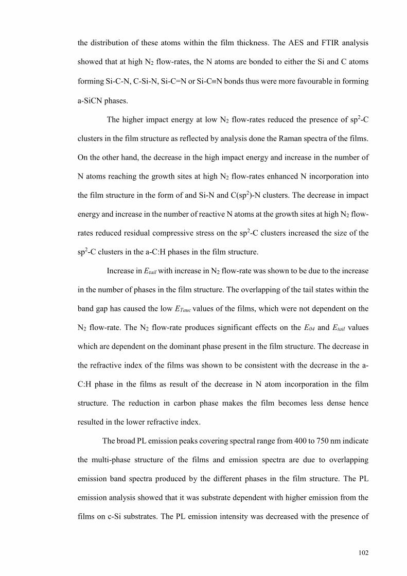
102
the distribution of these atoms within the film thickness. The AES and FTIR analysis
showed that at high N2 flow-rates, the N atoms are bonded to either the Si and C atoms
forming Si-C-N, C-Si-N, Si-C=N or Si-CN bonds thus were more favourable in forming
a-SiCN phases.
The higher impact energy at low N2 flow-rates reduced the presence of sp2-C
clusters in the film structure as reflected by analysis done the Raman spectra of the films.
On the other hand, the decrease in the high impact energy and increase in the number of
N atoms reaching the growth sites at high N2 flow-rates enhanced N incorporation into
the film structure in the form of and Si-N and C(sp2)-N clusters. The decrease in impact
energy and increase in the number of reactive N atoms at the growth sites at high N2 flow-
rates reduced residual compressive stress on the sp2-C clusters increased the size of the
sp2-C clusters in the a-C:H phases in the film structure.
Increase in Etail with increase in N2 flow-rate was shown to be due to the increase
in the number of phases in the film structure. The overlapping of the tail states within the
band gap has caused the low ETauc values of the films, which were not dependent on the
N2 flow-rate. The N2 flow-rate produces significant effects on the E04 and Etail values
which are dependent on the dominant phase present in the film structure. The decrease in
the refractive index of the films was shown to be consistent with the decrease in the a-
C:H phase in the films as result of the decrease in N atom incorporation in the film
structure. The reduction in carbon phase makes the film becomes less dense hence
resulted in the lower refractive index.
The broad PL emission peaks covering spectral range from 400 to 750 nm indicate
the multi-phase structure of the films and emission spectra are due to overlapping
emission band spectra produced by the different phases in the film structure. The PL
emission analysis showed that it was substrate dependent with higher emission from the
films on c-Si substrates. The PL emission intensity was decreased with the presence of
103
N2 in the deposition process of the films in this work. The a-SiCN: H films on c-Si
produced PL emission peaks at 2.81, 2.41, 2.30, 2.13 and 1.85 eV. The PL emission band
at 2.3 eV was only present in the films deposited with N2. Analysis of the results strongly
suggested that the origin of the weak PL emission at 2.81 eV was attributed recombination
process in the defects states in the region where the carbon clusters are surrounded by Si-
C matrix.
PL emission at 2.41 eV and 2.3 eV was proposed to be from the recombination
within tail states of a-CN:H and a-SiCN:H phases in the film structure where the tail states
are formed from C(sp2)-N clusters instead of C(sp2)-C clusters in the film. The origin of
the lowest energy PL emission at 1.85 eV was attributed to radiative recombination in the
tail states of H related bonds in the film structure formed from N-H or Si-H bonds. The
intense PL emission from the film deposited without N2 at 2.13 eV was supressed in the
films with N2. The PL emission was proposed to occur through recombination within tail
states of a-C:H in the films where the tail states are formed from sp2-C clusters in the
film. PL emission was shown to be substrate dependent.
PL intensity for the films on glass substrates was significantly lower compared to
the intensity of the films on c-Si substrates. Only two PL emission peaks were present
with the dominant peak at around 2.17 to 2.3 eV which from above analysis had its origin
recombination within tail states of the a-C:H phase. The lower intensity of the PL
emission showed that the sp2 clusters and the defect densities in the a-C:H phase are
smaller in size in the films on glass substrates.
104
CHAPTER 5: EFFECTS OF AGEING AND ANNEALING TEMPERATURE ON
AMORPHOUS SILICON CARBON NITRIDES THIN FILMS
5.1 Introduction
Ageing and annealing effects on the properties of silicon and carbon based films
have been a major concern in many studies as the stability of the film properties on
exposure to normal atmospheric environment with time and thermal effects on the film
properties are crucial in the applications of these materials in devices (Fernandez-Ramos
et al., 2003; Kozak et al., 2015; Persheyev et al., 2005). In this chapter, two important
issues affecting the structural and optical properties of a-SiC:H and a-SiCN:H films are
studied. The stability of these properties with respect to ageing in atmospheric
environment and thermal annealing are discussed and analysed. The ageing effects of
films exposed to atmospheric environment for 30 days are studied with respect to the
structural properties which include the chemical bonding properties and microstructural
properties measured from the Fourier transform infrared (FTIR) and micro Raman
scattering spectra of the films respectively.
These properties obtained from films deposited by PECVD from the discharge
of SiH4 and CH4 without and with N2 at different flow-rates are studied and analysed. The
films deposited at N2 flow-rate of 10 and 40 sccm are chosen based on their ageing
properties to represent films deposited at low and high N2 flow-rates respectively for the
studies on the effects of annealing on the structural and optical properties of the films.
FTIR, Raman scattering, optical transmittance and reflectance spectra of the films are
analysed in great details. The FTIR and Raman spectra analysis are done on films
deposited on c-Si substrates while the optical transmission and reflection spectra analysis
are done on films deposited on glass substrates. The bonding properties, microstructural
properties, band gap energy and refractive index of the multi-phase structure of the a-
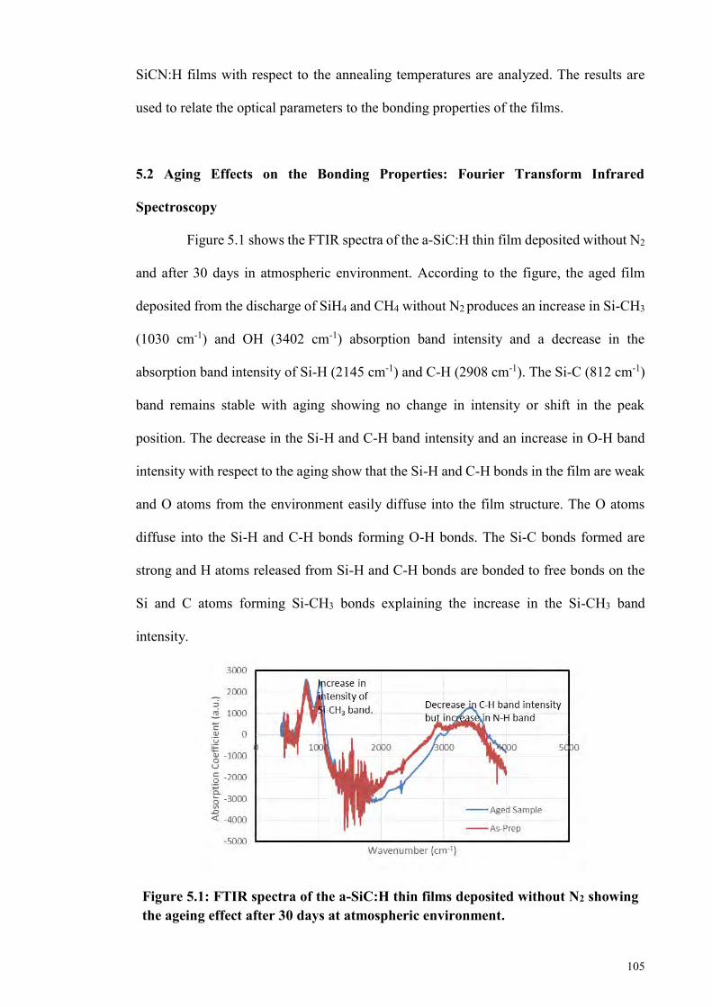
105
SiCN:H films with respect to the annealing temperatures are analyzed. The results are
used to relate the optical parameters to the bonding properties of the films.
5.2 Aging Effects on the Bonding Properties: Fourier Transform Infrared
Spectroscopy
Figure 5.1 shows the FTIR spectra of the a-SiC:H thin film deposited without N2
and after 30 days in atmospheric environment. According to the figure, the aged film
deposited from the discharge of SiH4 and CH4 without N2 produces an increase in Si-CH3
(1030 cm-1) and OH (3402 cm-1) absorption band intensity and a decrease in the
absorption band intensity of Si-H (2145 cm-1) and C-H (2908 cm-1). The Si-C (812 cm-1)
band remains stable with aging showing no change in intensity or shift in the peak
position. The decrease in the Si-H and C-H band intensity and an increase in O-H band
intensity with respect to the aging show that the Si-H and C-H bonds in the film are weak
and O atoms from the environment easily diffuse into the film structure. The O atoms
diffuse into the Si-H and C-H bonds forming O-H bonds. The Si-C bonds formed are
strong and H atoms released from Si-H and C-H bonds are bonded to free bonds on the
Si and C atoms forming Si-CH3 bonds explaining the increase in the Si-CH3 band
intensity.
Figure 5.1: FTIR spectra of the a-SiC:H thin films deposited without N2 showing the ageing effect after 30 days at atmospheric environment.
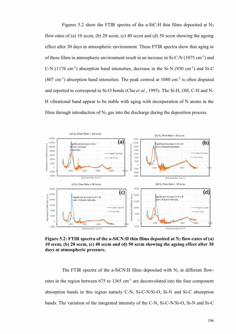
106
Figures 5.2 show the FTIR spectra of the a-SiC:H thin films deposited at N2
flow-rates of (a) 10 sccm, (b) 20 sccm, (c) 40 sccm and (d) 50 sccm showing the ageing
effect after 30 days in atmospheric environment. These FTIR spectra show that aging in
of these films in atmospheric environment result in an increase in Si-C-N (1075 cm-1) and
C-N (1176 cm-1) absorption band intensities, decrease in the Si-N (930 cm-1) and Si-C
(807 cm-1) absorption band intensities. The peak centred at 1080 cm-1 is often disputed
and reported to correspond to Si-O bonds (Chu et al., 1995). The Si-H, OH, C-H and N-
H vibrational band appear to be stable with aging with incorporation of N atoms in the
films through introduction of N2 gas into the discharge during the deposition process.
Figure 5.2: FTIR spectra of the a-SiCN:H thin films deposited at N2 flow-rates of (a) 10 sccm, (b) 20 sccm, (c) 40 sccm and (d) 50 sccm showing the ageing effect after 30 days at atmospheric pressure.
The FTIR spectra of the a-SiCN:H films deposited with N2 at different flow-
rates in the region between 675 to 1365 cm-1 are deconvoluted into the four component
absorption bands in this region namely C-N, Si-C-N/Si-O, Si-N and Si-C absorption
bands. The variation of the integrated intensity of the C-N, Si-C-N/Si-O, Si-N and Si-C
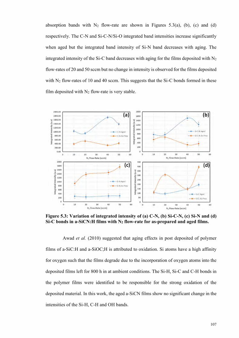
107
absorption bands with N2 flow-rate are shown in Figures 5.3(a), (b), (c) and (d)
respectively. The C-N and Si-C-N/Si-O integrated band intensities increase significantly
when aged but the integrated band intensity of Si-N band decreases with aging. The
integrated intensity of the Si-C band decreases with aging for the films deposited with N2
flow-rates of 20 and 50 sccm but no change in intensity is observed for the films deposited
with N2 flow-rates of 10 and 40 sccm. This suggests that the Si-C bonds formed in these
film deposited with N2 flow-rate is very stable.
Figure 5.3: Variation of integrated intensity of (a) C-N, (b) Si-C-N, (c) Si-N and (d) Si-C bonds in a-SiCN:H films with N2 flow-rate for as-prepared and aged films.
Awad et al. (2010) suggested that aging effects in post deposited of polymer
films of a-SiC:H and a-SiOC;H is attributed to oxidation. Si atoms have a high affinity
for oxygen such that the films degrade due to the incorporation of oxygen atoms into the
deposited films left for 800 h in at ambient conditions. The Si-H, Si-C and C-H bonds in
the polymer films were identified to be responsible for the strong oxidation of the
deposited material. In this work, the aged a-SiCN films show no significant change in the
intensities of the Si-H, C-H and OH bands.
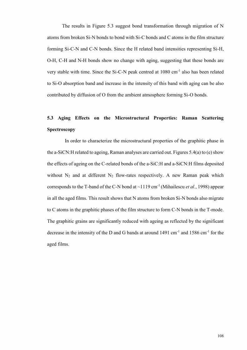
108
The results in Figure 5.3 suggest bond transformation through migration of N
atoms from broken Si-N bonds to bond with Si-C bonds and C atoms in the film structure
forming Si-C-N and C-N bonds. Since the H related band intensities representing Si-H,
O-H, C-H and N-H bonds show no change with aging, suggesting that these bonds are
very stable with time. Since the Si-C-N peak centred at 1080 cm-1 also has been related
to Si-O absorption band and increase in the intensity of this band with aging can be also
contributed by diffusion of O from the ambient atmosphere forming Si-O bonds.
5.3 Aging Effects on the Microstructural Properties: Raman Scattering
Spectroscopy
In order to characterize the microstructural properties of the graphitic phase in
the a-SiCN:H related to ageing, Raman analyses are carried out. Figures 5.4(a) to (e) show
the effects of ageing on the C-related bonds of the a-SiC:H and a-SiCN:H films deposited
without N2 and at different N2 flow-rates respectively. A new Raman peak which
corresponds to the T-band of the C-N bond at ~1119 cm-1 (Mihailescu et al., 1998) appear
in all the aged films. This result shows that N atoms from broken Si-N bonds also migrate
to C atoms in the graphitic phases of the film structure to form C-N bonds in the T-mode.
The graphitic grains are significantly reduced with ageing as reflected by the significant
decrease in the intensity of the D and G bands at around 1491 cm-1 and 1586 cm-1 for the
aged films.
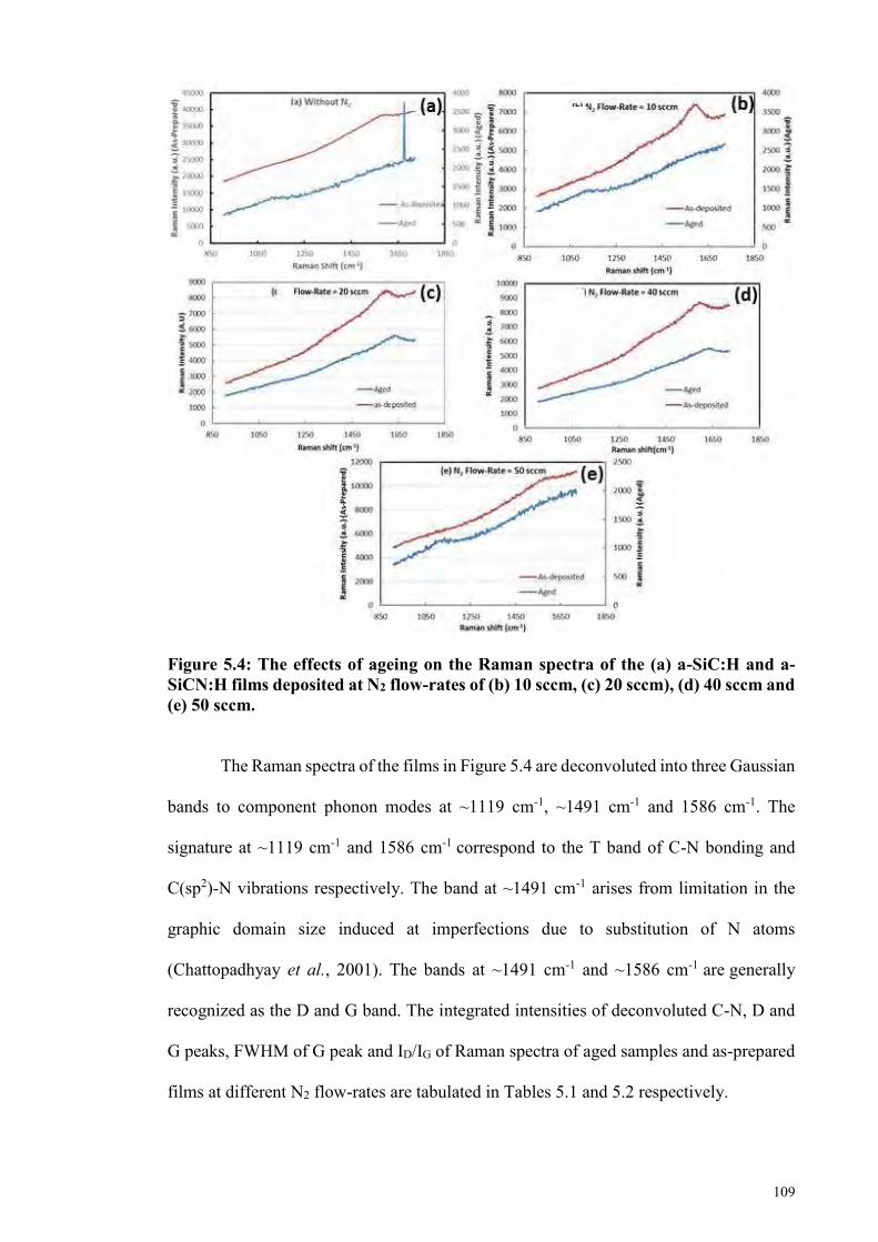
109
Figure 5.4: The effects of ageing on the Raman spectra of the (a) a-SiC:H and a-SiCN:H films deposited at N2 flow-rates of (b) 10 sccm, (c) 20 sccm), (d) 40 sccm and (e) 50 sccm.
The Raman spectra of the films in Figure 5.4 are deconvoluted into three Gaussian
bands to component phonon modes at ~1119 cm-1, ~1491 cm-1 and 1586 cm-1. The
signature at ~1119 cm-1 and 1586 cm-1 correspond to the T band of C-N bonding and
C(sp2)-N vibrations respectively. The band at ~1491 cm-1 arises from limitation in the
graphic domain size induced at imperfections due to substitution of N atoms
(Chattopadhyay et al., 2001). The bands at ~1491 cm-1 and ~1586 cm-1 are generally
recognized as the D and G band. The integrated intensities of deconvoluted C-N, D and
G peaks, FWHM of G peak and ID/IG of Raman spectra of aged samples and as-prepared
films at different N2 flow-rates are tabulated in Tables 5.1 and 5.2 respectively.
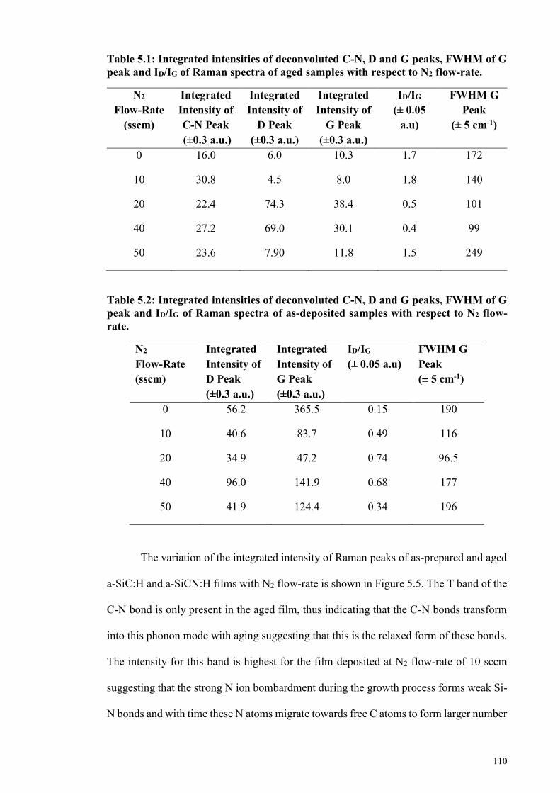
110
Table 5.1: Integrated intensities of deconvoluted C-N, D and G peaks, FWHM of G peak and ID/IG of Raman spectra of aged samples with respect to N2 flow-rate.
N2 Flow-Rate
(sscm)
Integrated Intensity of C-N Peak (±0.3 a.u.)
Integrated Intensity of
D Peak (±0.3 a.u.)
Integrated Intensity of
G Peak (±0.3 a.u.)
ID/IG
(± 0.05 a.u)
FWHM G Peak
(± 5 cm-1)
0 16.0 6.0 10.3 1.7 172
10 30.8 4.5 8.0 1.8 140
20 22.4 74.3 38.4 0.5 101
40 27.2 69.0 30.1 0.4 99
50 23.6 7.90 11.8 1.5 249
Table 5.2: Integrated intensities of deconvoluted C-N, D and G peaks, FWHM of G peak and ID/IG of Raman spectra of as-deposited samples with respect to N2 flow-rate.
N2 Flow-Rate (sscm)
Integrated Intensity of D Peak (±0.3 a.u.)
Integrated Intensity of G Peak (±0.3 a.u.)
ID/IG
(± 0.05 a.u) FWHM G Peak (± 5 cm-1)
0 56.2 365.5 0.15 190
10 40.6 83.7 0.49 116
20 34.9 47.2 0.74 96.5
40 96.0 141.9 0.68 177
50 41.9 124.4 0.34 196
The variation of the integrated intensity of Raman peaks of as-prepared and aged
a-SiC:H and a-SiCN:H films with N2 flow-rate is shown in Figure 5.5. The T band of the
C-N bond is only present in the aged film, thus indicating that the C-N bonds transform
into this phonon mode with aging suggesting that this is the relaxed form of these bonds.
The intensity for this band is highest for the film deposited at N2 flow-rate of 10 sccm
suggesting that the strong N ion bombardment during the growth process forms weak Si-
N bonds and with time these N atoms migrate towards free C atoms to form larger number
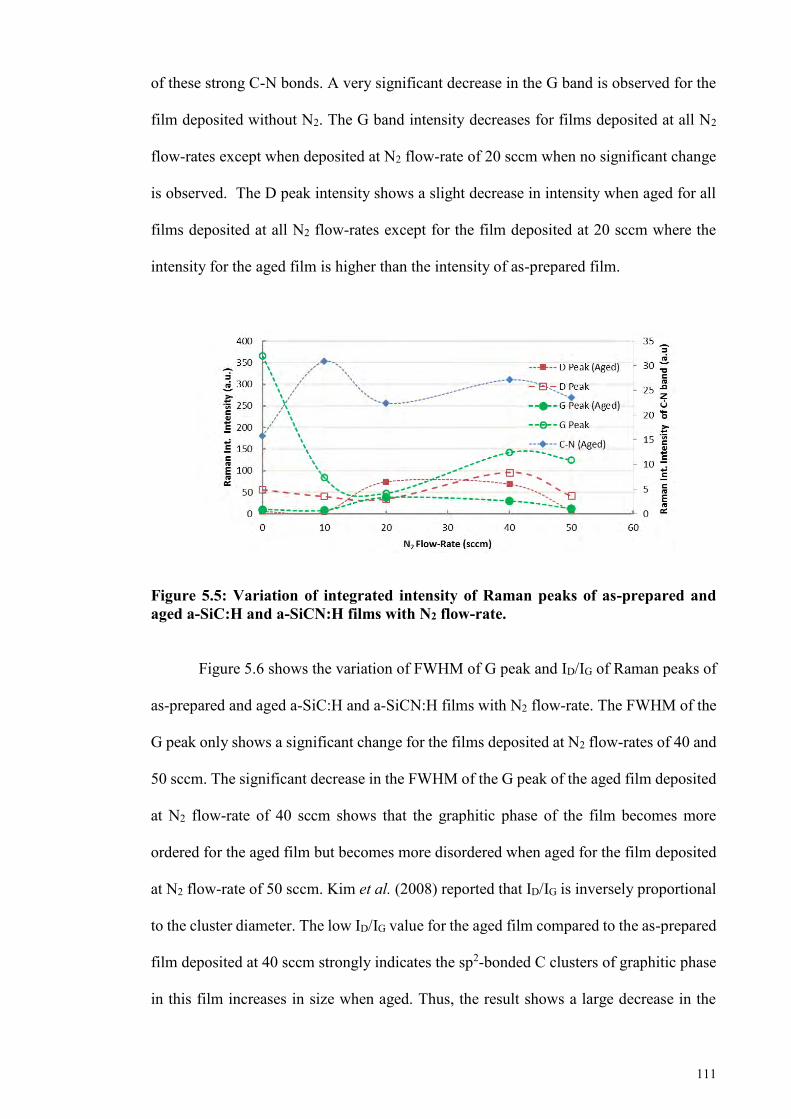
111
of these strong C-N bonds. A very significant decrease in the G band is observed for the
film deposited without N2. The G band intensity decreases for films deposited at all N2
flow-rates except when deposited at N2 flow-rate of 20 sccm when no significant change
is observed. The D peak intensity shows a slight decrease in intensity when aged for all
films deposited at all N2 flow-rates except for the film deposited at 20 sccm where the
intensity for the aged film is higher than the intensity of as-prepared film.
Figure 5.5: Variation of integrated intensity of Raman peaks of as-prepared and aged a-SiC:H and a-SiCN:H films with N2 flow-rate.
Figure 5.6 shows the variation of FWHM of G peak and ID/IG of Raman peaks of
as-prepared and aged a-SiC:H and a-SiCN:H films with N2 flow-rate. The FWHM of the
G peak only shows a significant change for the films deposited at N2 flow-rates of 40 and
50 sccm. The significant decrease in the FWHM of the G peak of the aged film deposited
at N2 flow-rate of 40 sccm shows that the graphitic phase of the film becomes more
ordered for the aged film but becomes more disordered when aged for the film deposited
at N2 flow-rate of 50 sccm. Kim et al. (2008) reported that ID/IG is inversely proportional
to the cluster diameter. The low ID/IG value for the aged film compared to the as-prepared
film deposited at 40 sccm strongly indicates the sp2-bonded C clusters of graphitic phase
in this film increases in size when aged. Thus, the result shows a large decrease in the
112
size of sp2-bonded C clusters in the graphitic phase of film deposited at N2 flow-rates of
10 and 50 sccm when aged.
Figure 5.6: Variation of FWHM of G peak and ID/IG of Raman peaks of the as-prepared and aged a-SiC:H and a-SiCN:H films with different N2 flow-rate.
These results imply that N2 flow-rate of 40 sccm produces the optimum N ion
bombardment effects to form a-SiCN:H films with graphitic phase which improves in the
structural order and increases the size of the sp2-bonded C clusters with aging in
atmospheric environments. The high N ion bombardments during growth of the film
deposited at N2 flow-rate of 10 sccm results in unstable bonds which result in increase in
structural disorder and decrease in the sp2-bonded C clusters when aged in atmospheric
environment.
5.4 Annealing Effects on the Bonding Properties: Fourier Transform Infrared
Spectroscopy
The effects of annealing are done on the films deposited at N2 flow-rates of 10
and 40 sccm based on the results obtained from the ageing studies presented in the
previous sections. The film deposited at N2 flow-rate of 10 sccm has the maximum N ion
bombardment effects resulting in structural properties which deteriorate with aging in
atmospheric environment. The film deposited at N2 flow-rate of 40 sccm on the other
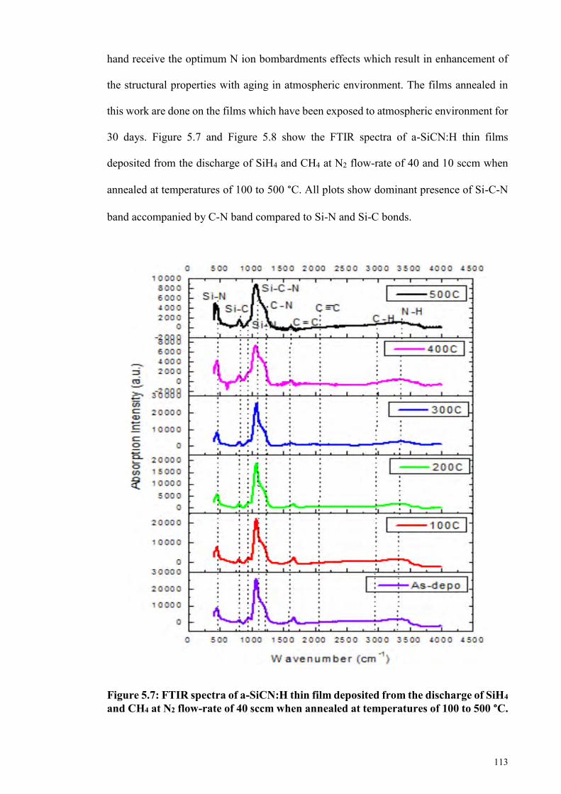
113
hand receive the optimum N ion bombardments effects which result in enhancement of
the structural properties with aging in atmospheric environment. The films annealed in
this work are done on the films which have been exposed to atmospheric environment for
30 days. Figure 5.7 and Figure 5.8 show the FTIR spectra of a-SiCN:H thin films
deposited from the discharge of SiH4 and CH4 at N2 flow-rate of 40 and 10 sccm when
annealed at temperatures of 100 to 500 °C. All plots show dominant presence of Si-C-N
band accompanied by C-N band compared to Si-N and Si-C bonds.
Figure 5.7: FTIR spectra of a-SiCN:H thin film deposited from the discharge of SiH4 and CH4 at N2 flow-rate of 40 sccm when annealed at temperatures of 100 to 500 °C.
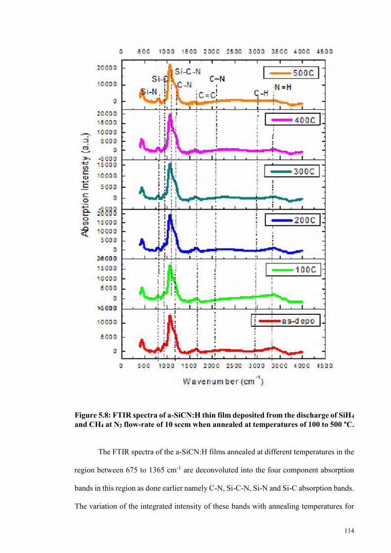
114
Figure 5.8: FTIR spectra of a-SiCN:H thin film deposited from the discharge of SiH4 and CH4 at N2 flow-rate of 10 sccm when annealed at temperatures of 100 to 500 °C.
The FTIR spectra of the a-SiCN:H films annealed at different temperatures in the
region between 675 to 1365 cm-1 are deconvoluted into the four component absorption
bands in this region as done earlier namely C-N, Si-C-N, Si-N and Si-C absorption bands.
The variation of the integrated intensity of these bands with annealing temperatures for
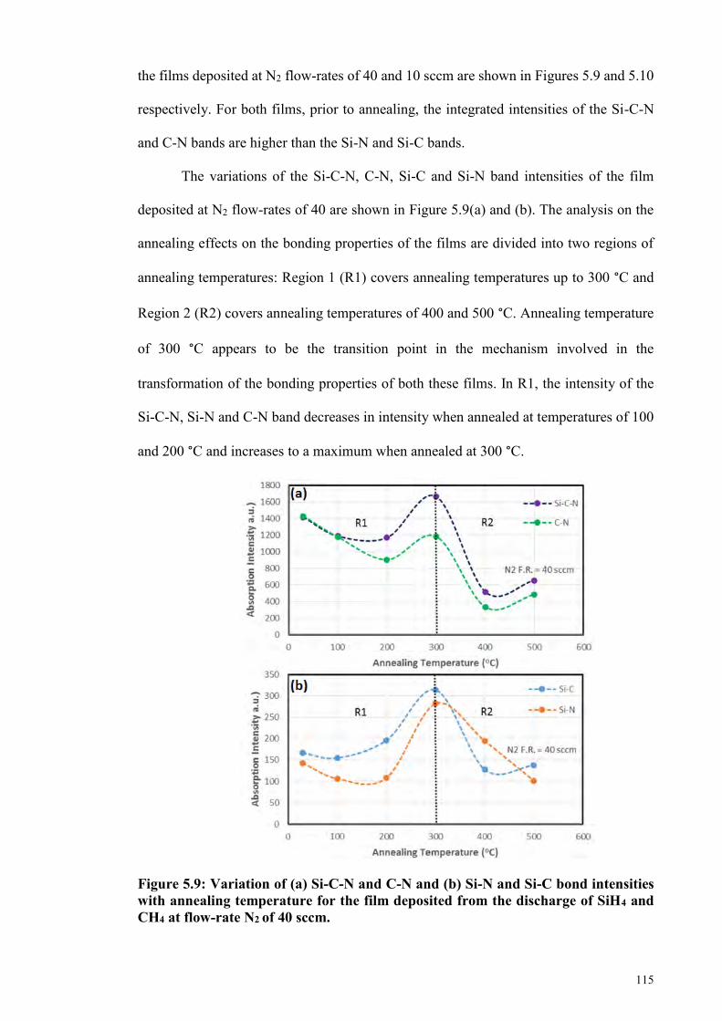
115
the films deposited at N2 flow-rates of 40 and 10 sccm are shown in Figures 5.9 and 5.10
respectively. For both films, prior to annealing, the integrated intensities of the Si-C-N
and C-N bands are higher than the Si-N and Si-C bands.
The variations of the Si-C-N, C-N, Si-C and Si-N band intensities of the film
deposited at N2 flow-rates of 40 are shown in Figure 5.9(a) and (b). The analysis on the
annealing effects on the bonding properties of the films are divided into two regions of
annealing temperatures: Region 1 (R1) covers annealing temperatures up to 300 °C and
Region 2 (R2) covers annealing temperatures of 400 and 500 °C. Annealing temperature
of 300 °C appears to be the transition point in the mechanism involved in the
transformation of the bonding properties of both these films. In R1, the intensity of the
Si-C-N, Si-N and C-N band decreases in intensity when annealed at temperatures of 100
and 200 °C and increases to a maximum when annealed at 300 °C.
Figure 5.9: Variation of (a) Si-C-N and C-N and (b) Si-N and Si-C bond intensities with annealing temperature for the film deposited from the discharge of SiH4 and CH4 at flow-rate N2 of 40 sccm.
116
The intensity of the C-N decreases at a faster rate compared to the other two band
intensities showing that N atoms out diffuse from the C-N bonds at a faster rate suggesting
that the N atoms in the C-N bonds are more loosely bonded compared to the N atoms in
Si-C-N and Si-N bonds. The Si-C-N and C-N band intensities decrease steeply to a
minimum when annealed at 400 °C and increases again slightly when annealed at
temperature of 500 °C in R2. The Si-N band intensity decreases continuously when
annealed at 400 and 500 °C. The Si-C band intensity shows a continuous increasing trend
to a maximum when annealed at 300 °C in R1 and a decrease in intensity to a minimum
when annealed at 400 °C and remains constant when annealed further at 500 °C in R2.
Fernandez-Ramos et al. (2000 & 2003) reported in their work on the effects of annealing
on Si doped carbon nitride and pure carbon nitride films that N atoms are released from
these films when annealed between temperatures of 200 and 350 °C as deduced from the
constant decrease in N to C ratio of these films when annealed. Therefore, the decrease
in the Si-C-N, Si-N and C-N band intensity annealed at 100- 200 °C can be attributed to
the out diffusion process of N atoms from weak C-N, Si-N and Si-C-N bonds.
These N atoms remains trapped in the film structure as the thermal energy is not
sufficient to release these atoms from the film. The low N ion bombardment during the
growth process as a result of the low N2 flow-rate also leaves trapped N atoms within the
vacancy regions in the film structure. Diffusion of these N atoms into the film structure
forming stronger bonds to Si and C atoms may contribute to the increase in C-N, Si-N
and Si-C-N band intensities when annealed at 300 °C. Further annealing at 400 °C
decreases these band intensities as the thermal energy at this annealing temperature is
sufficient to break C-N and Si-N bonds releasing N atoms from the film structure. The
Si-N band intensity continues to decrease when annealed at 500 °C and the N atoms
released from these bonds are diffused into free C bonds to form Si-C-N and C-N bonds
explaining the slight increase intensities of the Si-C-N and C-N band intensities.
117
Restructuring of free Si and C bonds left by the out-diffusion of N atoms increases the
band intensity of the Si-C band when annealed at temperatures of 100, 200 and 300 °C.
It is observed from the analysis above that the film deposited at N2 flow-rate of
40 sccm after aging process consists of N atoms bonded to Si and C atoms forming Si-N,
C-N and Si-C-N bonds forming a-SiN, a-CN and a-SiCN phases. The N atoms are either
weakly or strongly bonded to the Si and C atoms. The first phase of out-diffusion of N
atoms occurs when the film is annealed at 100 and 200 °C but these N atoms remains the
film structure as trapped N atoms. Annealing temperature of 300 °C provide sufficient
thermal energy for restructuring involving the formation of Si-C and strong C-N and Si-
N bonds. The second phase of out-diffusion and evolution of N atoms happens when the
film is annealed at 400 °C and this involved more N atoms as compared to the number of
N atoms released from Si and C atoms when the film is annealed at 200 °C. Another phase
of restructuring occurs at annealing temperature of 500 °C involving migration of N atoms
from Si-N bonds to form C-N bonds and bonding of the Si bonds vacated by the N atoms
to C atoms forming Si-C bonds.
The variations of the Si-C-N, C-N, Si-C and Si-N band intensities of the film
deposited at N2 flow-rate of 10 sccm are shown in Figure 5.10(a) and (b). The Si-C and
C-N band intensities follow similar trends with increase in these band intensities when
annealed at 100 °C and remain constant when annealed at 200 °C in R1. These band
intensities decrease when annealed at 300 °C. In R2, these band intensities increase to a
continuously when annealed further at 400 and 500 °C. The Si-C-N band intensity
increases and decreases alternately when annealed at temperatures of 100, 200 and 300
°C in Region 1.
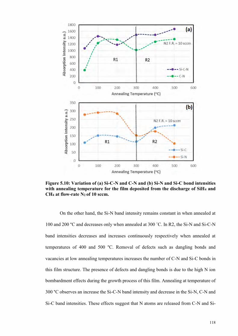
118
Figure 5.10: Variation of (a) Si-C-N and C-N and (b) Si-N and Si-C bond intensities with annealing temperature for the film deposited from the discharge of SiH4 and CH4 at flow-rate N2 of 10 sccm.
On the other hand, the Si-N band intensity remains constant in when annealed at
100 and 200 °C and decreases only when annealed at 300 ˚C. In R2, the Si-N and Si-C-N
band intensities decreases and increases continuously respectively when annealed at
temperatures of 400 and 500 °C. Removal of defects such as dangling bonds and
vacancies at low annealing temperatures increases the number of C-N and Si-C bonds in
this film structure. The presence of defects and dangling bonds is due to the high N ion
bombardment effects during the growth process of this film. Annealing at temperature of
300 °C observes an increase the Si-C-N band intensity and decrease in the Si-N, C-N and
Si-C band intensities. These effects suggest that N atoms are released from C-N and Si-
119
N bond and are diffused into Si-C bonds forming more Si-C-N bonds which also explains
the decrease in the Si-C bond intensity. Active restructuring appears to occur when
annealed at temperature of 400 °C, as the Si-C and C-N band intensities show a noticeable
increase compared to the Si-N and Si-C-N band intensities.
Figures 5.11(a), (b) and (c) show the variations of the ratio of Si-N, C-N and Si-
C band intensity to the Si-C-N band intensity labelled as Si-N/Si-C-N, C-N/Si-C-N and
Si-C/Si-C-N respectively. Analysis on the variation of these parameters with respect to
the annealing temperature is to complement the above analysis since Si-N, C-N and Si-C
can be component bonds of the Si-C-N bond to form the a-SiCN phase or isolated bonds
from the Si-C-N bonds forming the a-SiN, a-CN or a-SiC phases in the film structure.
From the FTIR analysis, since the Si-C-N bonds have their own phonon band, these bonds
are assumed to originate from the a-SiCN phase while the Si-N, C-N and Si-C bond are
bonds formed in the a-SiN, a-CN and a-SiC phases. R1 and R2 in these figures cover the
same annealing temperature range assigned in Figures 5.9 and 5.10.
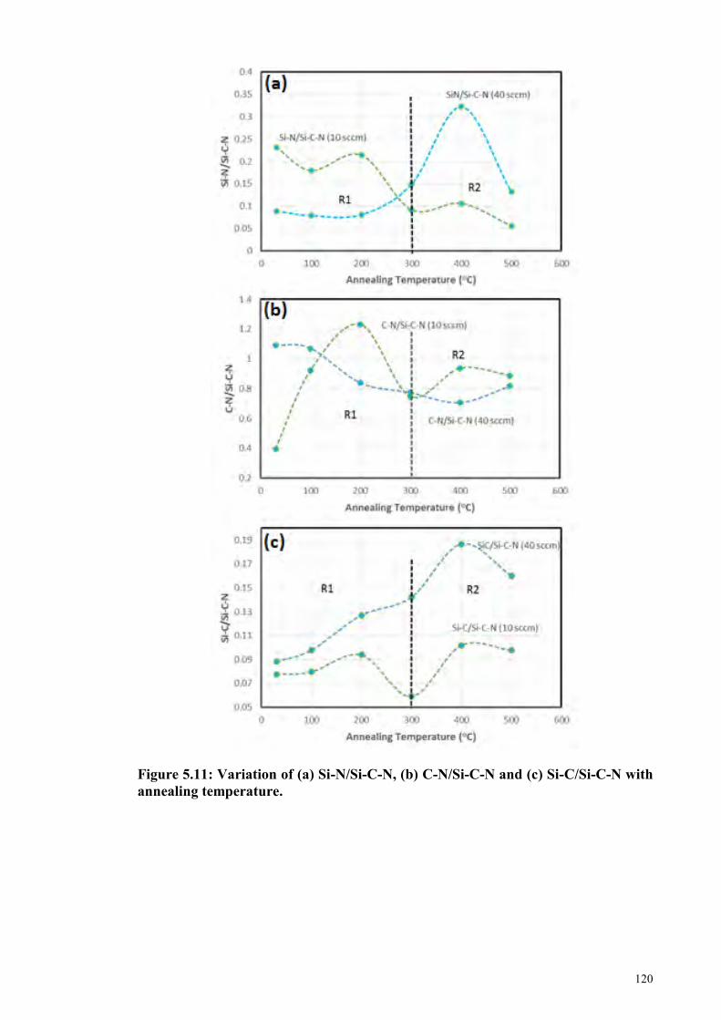
120
Figure 5.11: Variation of (a) Si-N/Si-C-N, (b) C-N/Si-C-N and (c) Si-C/Si-C-N with annealing temperature.
121
It is demonstrated in Figure 5.11(a), (b) and (c) that C-N bonds are the most
dominant bonds with respect to the Si-C-N bonds in the structure of film deposited at N2
flow-rate of 10 and 40 sccm suggesting that the a-CN phase is the most dominant phase
compared to a-SiN and a-SiC phases with respect to the a-SiCN phase in these film
structures. In fact, for the as-deposited film and the film annealed at 100 °C, for the film
deposited at N2 flow-rate of 10 sccm and the film annealed at 200 °C, for the film
deposited at N2 flow-rate of 40 sccm, the a-CN phase is more dominant than the a-SiCN
phase since the ratio exceeds 1.
The a-CN phase increases in dominance when annealed at 100 and 200 °C. When
annealed at 300 °C, both a-SiN and a-SiC phases increases while the a-CN phase
decreases although the a-CN is still the most dominant phase besides the a-SiCN phase.
In R2, the a-SiN and a-SiC phases continue to increase along with the a-CN phase. Thus,
it can be seen here that the number of component phases increases when annealed at
temperatures of 300 and 400 °C. The a-SiN, a-CN and a-SiC phases decreases with
respect to the a-SiCN when annealed at 500 °C. In Figure 5.11(a), it can be seen that in
R1, the a-SiN phase is higher in the film deposited at N2 flow-rate of 10 sccm while in
R2, it is reversed with the increase in dominance of the a-SiN phase when the film is
annealed at 400 °C.
Figure 5.11(b) shows that in the a-CN phase is higher in the film deposited at N2
flow-rate of 40 sccm when as-prepared and when annealed at 100 °C. Then it continues
to decrease when annealed at 200 and 300 °C in R1. The a-CN in the film deposited at N2
flow-rate of 10 sccm preaches a maximum when annealed at 200 °C. In R2, the a-CN of
the film deposited at N2 flow-rate of 40 sccm decreases and increases again when
annealed at 400 and 500 °C respectively. The reversed trend is observed for the film
deposited at N2 flow-rate of 10 sccm with the a-CN phase being more dominant in this
region compared to the a-CN phase in the film deposited at N2 flow-rate of 40 sccm.
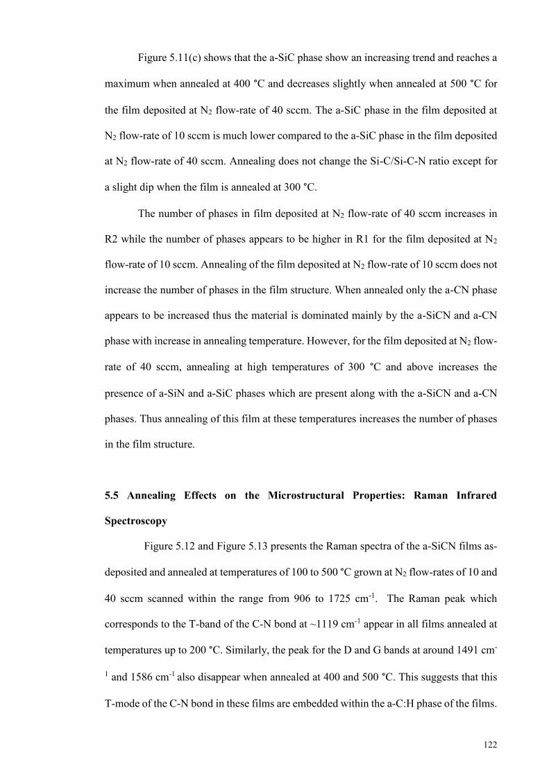
122
Figure 5.11(c) shows that the a-SiC phase show an increasing trend and reaches a
maximum when annealed at 400 °C and decreases slightly when annealed at 500 °C for
the film deposited at N2 flow-rate of 40 sccm. The a-SiC phase in the film deposited at
N2 flow-rate of 10 sccm is much lower compared to the a-SiC phase in the film deposited
at N2 flow-rate of 40 sccm. Annealing does not change the Si-C/Si-C-N ratio except for
a slight dip when the film is annealed at 300 °C.
The number of phases in film deposited at N2 flow-rate of 40 sccm increases in
R2 while the number of phases appears to be higher in R1 for the film deposited at N2
flow-rate of 10 sccm. Annealing of the film deposited at N2 flow-rate of 10 sccm does not
increase the number of phases in the film structure. When annealed only the a-CN phase
appears to be increased thus the material is dominated mainly by the a-SiCN and a-CN
phase with increase in annealing temperature. However, for the film deposited at N2 flow-
rate of 40 sccm, annealing at high temperatures of 300 °C and above increases the
presence of a-SiN and a-SiC phases which are present along with the a-SiCN and a-CN
phases. Thus annealing of this film at these temperatures increases the number of phases
in the film structure.
5.5 Annealing Effects on the Microstructural Properties: Raman Infrared
Spectroscopy
Figure 5.12 and Figure 5.13 presents the Raman spectra of the a-SiCN films as-
deposited and annealed at temperatures of 100 to 500 °C grown at N2 flow-rates of 10 and
40 sccm scanned within the range from 906 to 1725 cm-1. The Raman peak which
corresponds to the T-band of the C-N bond at ~1119 cm-1 appear in all films annealed at
temperatures up to 200 °C. Similarly, the peak for the D and G bands at around 1491 cm-
1 and 1586 cm-1 also disappear when annealed at 400 and 500 °C. This suggests that this
T-mode of the C-N bond in these films are embedded within the a-C:H phase of the films.
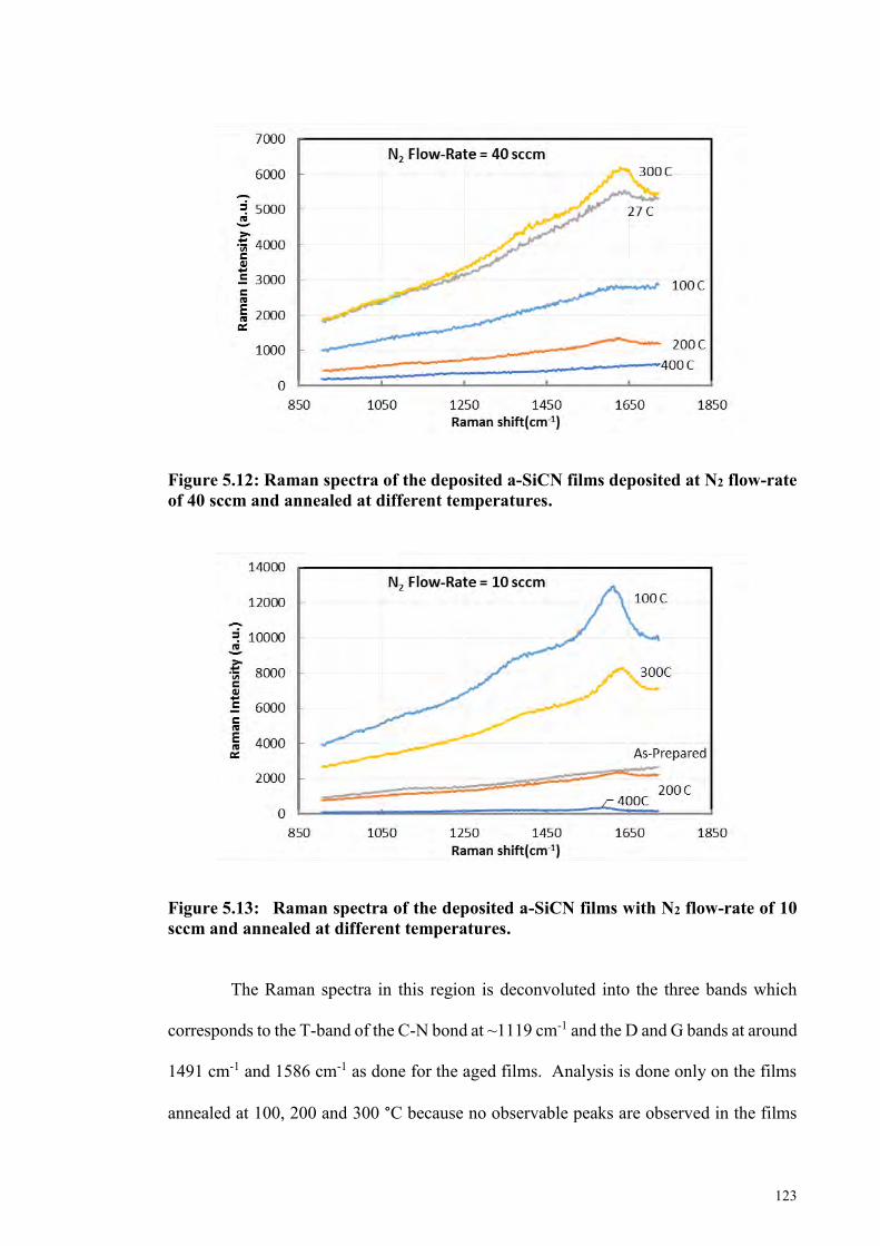
123
Figure 5.12: Raman spectra of the deposited a-SiCN films deposited at N2 flow-rate of 40 sccm and annealed at different temperatures.
Figure 5.13: Raman spectra of the deposited a-SiCN films with N2 flow-rate of 10 sccm and annealed at different temperatures.
The Raman spectra in this region is deconvoluted into the three bands which
corresponds to the T-band of the C-N bond at ~1119 cm-1 and the D and G bands at around
1491 cm-1 and 1586 cm-1 as done for the aged films. Analysis is done only on the films
annealed at 100, 200 and 300 °C because no observable peaks are observed in the films
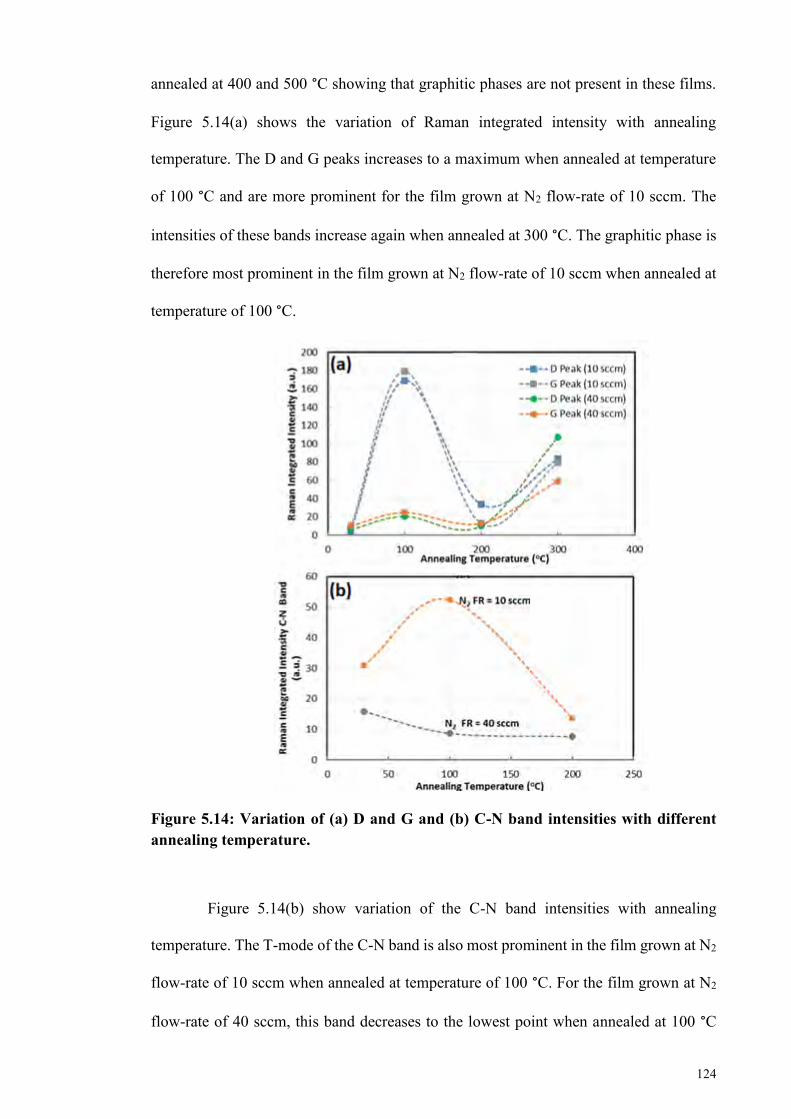
124
annealed at 400 and 500 °C showing that graphitic phases are not present in these films.
Figure 5.14(a) shows the variation of Raman integrated intensity with annealing
temperature. The D and G peaks increases to a maximum when annealed at temperature
of 100 °C and are more prominent for the film grown at N2 flow-rate of 10 sccm. The
intensities of these bands increase again when annealed at 300 °C. The graphitic phase is
therefore most prominent in the film grown at N2 flow-rate of 10 sccm when annealed at
temperature of 100 °C.
Figure 5.14: Variation of (a) D and G and (b) C-N band intensities with different annealing temperature.
Figure 5.14(b) show variation of the C-N band intensities with annealing
temperature. The T-mode of the C-N band is also most prominent in the film grown at N2
flow-rate of 10 sccm when annealed at temperature of 100 °C. For the film grown at N2
flow-rate of 40 sccm, this band decreases to the lowest point when annealed at 100 °C
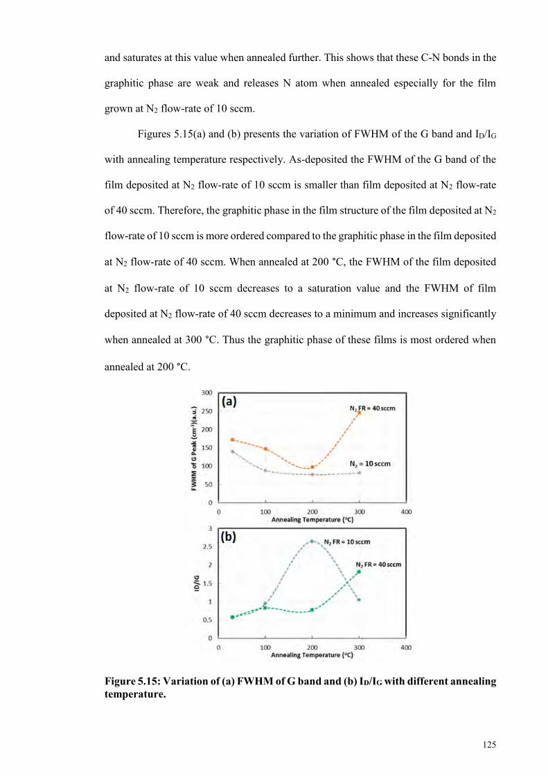
125
and saturates at this value when annealed further. This shows that these C-N bonds in the
graphitic phase are weak and releases N atom when annealed especially for the film
grown at N2 flow-rate of 10 sccm.
Figures 5.15(a) and (b) presents the variation of FWHM of the G band and ID/IG
with annealing temperature respectively. As-deposited the FWHM of the G band of the
film deposited at N2 flow-rate of 10 sccm is smaller than film deposited at N2 flow-rate
of 40 sccm. Therefore, the graphitic phase in the film structure of the film deposited at N2
flow-rate of 10 sccm is more ordered compared to the graphitic phase in the film deposited
at N2 flow-rate of 40 sccm. When annealed at 200 °C, the FWHM of the film deposited
at N2 flow-rate of 10 sccm decreases to a saturation value and the FWHM of film
deposited at N2 flow-rate of 40 sccm decreases to a minimum and increases significantly
when annealed at 300 °C. Thus the graphitic phase of these films is most ordered when
annealed at 200 °C.
Figure 5.15: Variation of (a) FWHM of G band and (b) ID/IG with different annealing temperature.
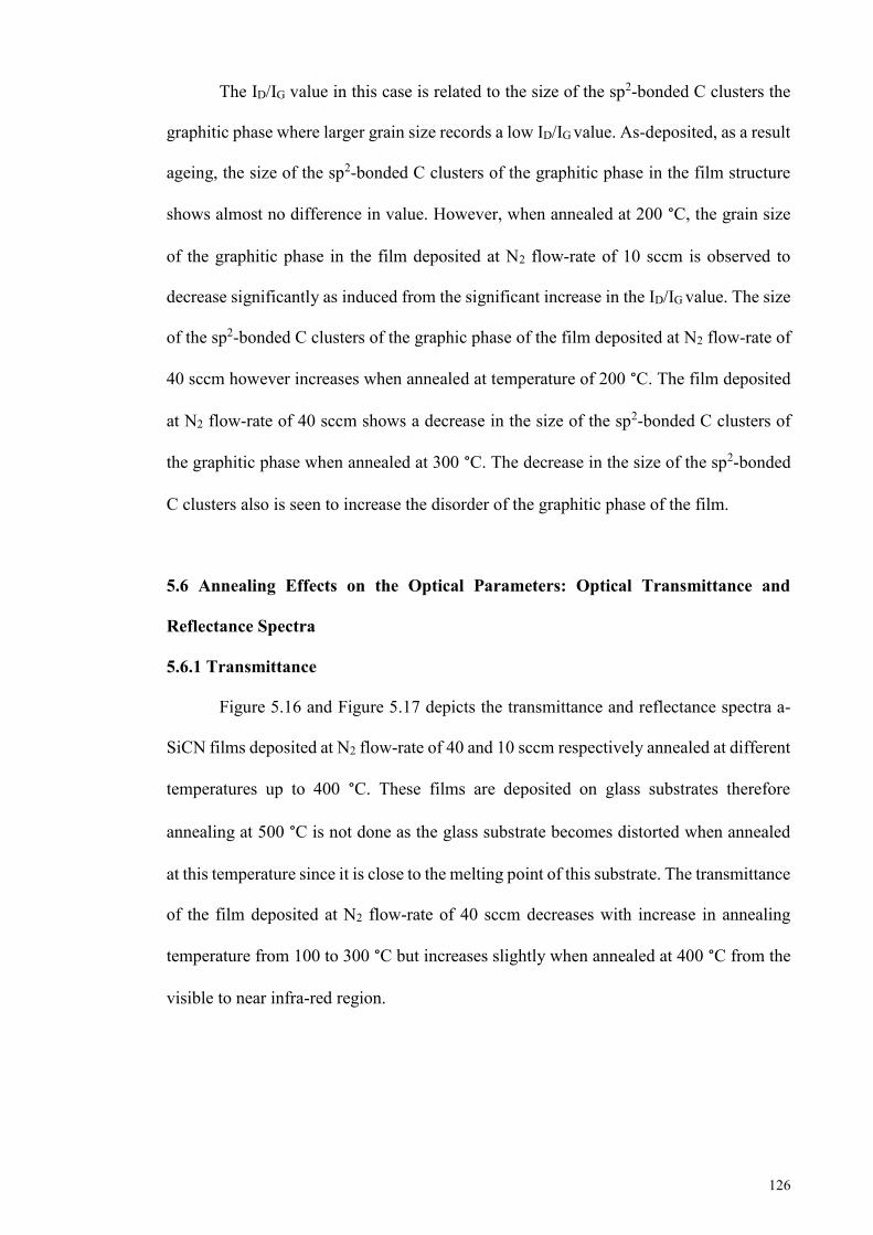
126
The ID/IG value in this case is related to the size of the sp2-bonded C clusters the
graphitic phase where larger grain size records a low ID/IG value. As-deposited, as a result
ageing, the size of the sp2-bonded C clusters of the graphitic phase in the film structure
shows almost no difference in value. However, when annealed at 200 °C, the grain size
of the graphitic phase in the film deposited at N2 flow-rate of 10 sccm is observed to
decrease significantly as induced from the significant increase in the ID/IG value. The size
of the sp2-bonded C clusters of the graphic phase of the film deposited at N2 flow-rate of
40 sccm however increases when annealed at temperature of 200 °C. The film deposited
at N2 flow-rate of 40 sccm shows a decrease in the size of the sp2-bonded C clusters of
the graphitic phase when annealed at 300 °C. The decrease in the size of the sp2-bonded
C clusters also is seen to increase the disorder of the graphitic phase of the film.
5.6 Annealing Effects on the Optical Parameters: Optical Transmittance and
Reflectance Spectra
5.6.1 Transmittance
Figure 5.16 and Figure 5.17 depicts the transmittance and reflectance spectra a-
SiCN films deposited at N2 flow-rate of 40 and 10 sccm respectively annealed at different
temperatures up to 400 °C. These films are deposited on glass substrates therefore
annealing at 500 °C is not done as the glass substrate becomes distorted when annealed
at this temperature since it is close to the melting point of this substrate. The transmittance
of the film deposited at N2 flow-rate of 40 sccm decreases with increase in annealing
temperature from 100 to 300 °C but increases slightly when annealed at 400 °C from the
visible to near infra-red region.
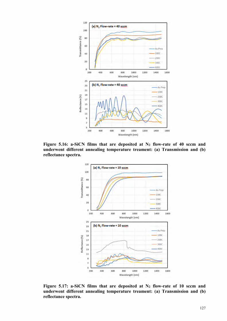
127
Figure 5.16: a-SiCN films that are deposited at N2 flow-rate of 40 sccm and underwent different annealing temperature treament: (a) Transmission and (b) reflectance spectra.
Figure 5.17: a-SiCN films that are deposited at N2 flow-rate of 10 sccm and underwent different annealing temperature treament: (a) Transmission and (b) reflectance spectra.
128
The film deposited at N2 flow-rate of 10 sccm shows decrease in transmittance
with increase in annealing temperature from 100 to 400 °C only in the visible region. The
transmittance of the film deposited at N2 flow-rate of 40 sccm decreases when annealed
at 100 °C but increases again with increase in annealing temperature from 200 to 400 °C
from the visible to near infra-red region. The reflectance of the film deposited at N2 flow-
rate of 10 sccm increases significantly when annealed at 200 °C but decreases again when
annealed at 300 °C and 400 °C. The film deposited at N2 flow-rate of 10 sccm produces a
systematic red shift of the absorption edge suggesting a systematic decrease in the band
gap of the film with increase in annealing temperature from 200 to 400 °C. The shift in
the absorption edge for the film deposited at N2 flow-rate of 40 sccm does not show a
consistent trend with annealing temperature.
5.6.2 Optical Energy Gap
Figure 5.18 shows the variation of the optical band gap energy (ETauc) and energy
at absorption of 104 cm (E04) with annealing temperature for films deposited at N2 flow-
rates of 10 and 40 sccm. These parameters have been obtained from the transmittance and
reflectance spectra using calculations detailed in Chapter 3. E04 represents the band edge
of the films while ETauc energy gap separating the highest localized states on the valence
band and the lowest localized states on the conduction band of the films.
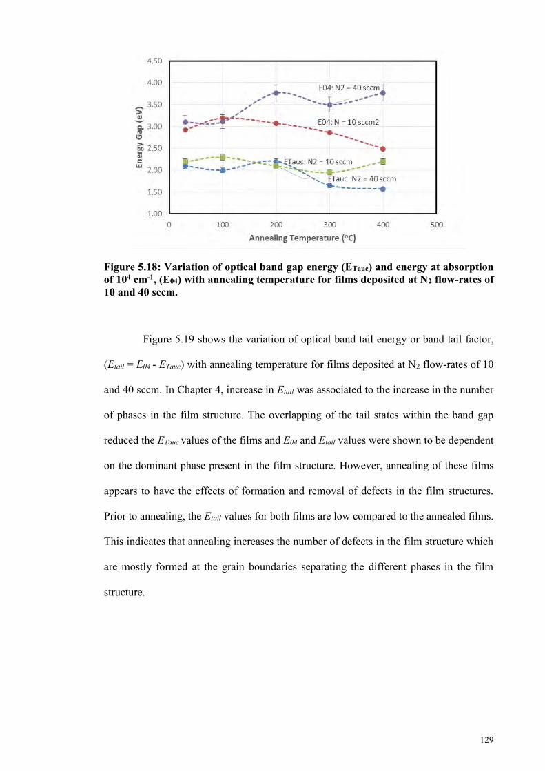
129
Figure 5.18: Variation of optical band gap energy (ETauc) and energy at absorption of 104 cm-1, (E04) with annealing temperature for films deposited at N2 flow-rates of 10 and 40 sccm.
Figure 5.19 shows the variation of optical band tail energy or band tail factor,
(Etail = E04 - ETauc) with annealing temperature for films deposited at N2 flow-rates of 10
and 40 sccm. In Chapter 4, increase in Etail was associated to the increase in the number
of phases in the film structure. The overlapping of the tail states within the band gap
reduced the ETauc values of the films and E04 and Etail values were shown to be dependent
on the dominant phase present in the film structure. However, annealing of these films
appears to have the effects of formation and removal of defects in the film structures.
Prior to annealing, the Etail values for both films are low compared to the annealed films.
This indicates that annealing increases the number of defects in the film structure which
are mostly formed at the grain boundaries separating the different phases in the film
structure.
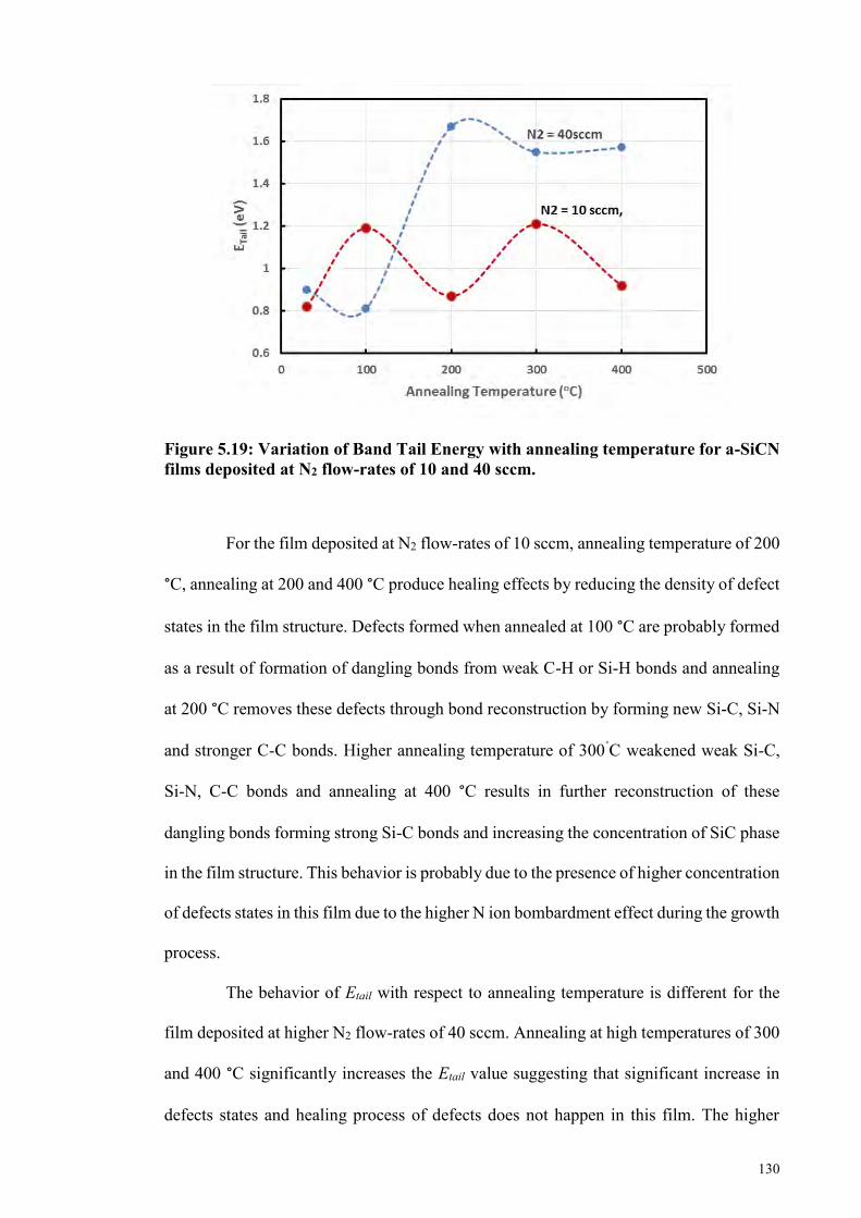
130
Figure 5.19: Variation of Band Tail Energy with annealing temperature for a-SiCN films deposited at N2 flow-rates of 10 and 40 sccm.
For the film deposited at N2 flow-rates of 10 sccm, annealing temperature of 200
°C, annealing at 200 and 400 °C produce healing effects by reducing the density of defect
states in the film structure. Defects formed when annealed at 100 °C are probably formed
as a result of formation of dangling bonds from weak C-H or Si-H bonds and annealing
at 200 °C removes these defects through bond reconstruction by forming new Si-C, Si-N
and stronger C-C bonds. Higher annealing temperature of 300˚C weakened weak Si-C,
Si-N, C-C bonds and annealing at 400 °C results in further reconstruction of these
dangling bonds forming strong Si-C bonds and increasing the concentration of SiC phase
in the film structure. This behavior is probably due to the presence of higher concentration
of defects states in this film due to the higher N ion bombardment effect during the growth
process.
The behavior of Etail with respect to annealing temperature is different for the
film deposited at higher N2 flow-rates of 40 sccm. Annealing at high temperatures of 300
and 400 °C significantly increases the Etail value suggesting that significant increase in
defects states and healing process of defects does not happen in this film. The higher
131
presence of N related bonds in this film structure results in evolution of the N atoms from
the film structure thus significantly increases the dangling bonds concentration which
forms vacancy related defects which are not easily healed through annealing.
E04 and ETauc for the film deposited at N2 flow-rate of 40 sccm increases to a
maximum when annealed at 200 °C. Increase in the annealing temperature to 300 °C
decreases the E04 value slightly and this value increases again slightly when annealing at
temperature of 400 °C. The ETauc continuously decreases when annealed at these
temperatures. As mentioned above E04 measures the energy gap of the film from the band
edges thus excluding the localized states in the band gap. ETauc measures the band gap
with the localized stated considered and therefore is smaller than E04.
The increase in E04 value in the film structure is usually related to the increase in
N incorporation into film structure. The decrease in ETauc when the film is annealed at
300 and 400 °C shows that the localized states in the film has increased when annealed at
these temperatures. Thus, the results imply that increase in annealing temperature to 200
°C have increased the quantity of N incorporation into the film structure and is also
accompanied by an increase in the number of phases in the film structure resulting in the
increase in structural disorder. The decrease in E04 in the film annealed at 300 °C can be
due to release of N atoms from broken C-N or Si-N which are not evolved but are trapped
in the film structure.
Restructuring of these broken bonds may result in the formation of Si-C bonds
when annealed at 400 °C thus increasing E04 again. Annealing at this temperature also
diffuses the trapped N atoms into the film structure through the formation of Si-N and C-
N bonds. The increase in number of phases due N atom incorporation and restructuring
of broken bonds maybe contributed by the formation multi-phase film structure with a-
SiN, a-CN, a-SiC phases and a-SiCN instead of a dominant phase of a-SiCN phase in the
132
film structure. However, the decrease in ETauc suggests increase in structural disorder
when the film is annealed at this temperature.
E04 for the film deposited at N2 flow-rate of 10 sccm decreases continuously when
annealed at 200 °C and above. This suggests that the N atoms in the film are loosely
bonded and the increase in thermal energy induced through the annealing process
continuously breaks weak N bonds and N atoms are evolved from the film structure. Out-
diffusion of N from these bonds contributed to the decrease in E04 and ETauc when
annealed at 200 and 300 °C. However, restructuring of broken bonds when annealed at
400 °C does not increase E04 but increases ETauc. This could be due to the fact that
restructuring here does not involve diffusion of N atoms into the film structure. The
increase in ETauc shows increase in structural order in the film structure when annealed at
400 °C. Figure 5.20(a) and (b) show the dispersion curves of the refractive indices of a-
SiCN films as-prepared and annealed at different temperatures for films deposited at N2
flow-rates of 10 and 40 sccm respectively. The refractive indices of the films deposited
at N2 flow-rate of 40 sccm when annealed at 200 and 300 °C demonstrates typical
behaviour of refractive index dispersion curve where the refractive index decreases to a
saturation value at long wavelengths. The as-deposited film and films annealed at 100
and 400 °C produce a refractive index dispersion curve which decreases steeply to a
minimum value at wavelength of 1500 nm and increases again beyond this wavelength.
The typical point of inflection for all films is at wavelengths around 1500 nm while for
the as-deposited film, this point of inflection occurs above 1500 nm wavelength.
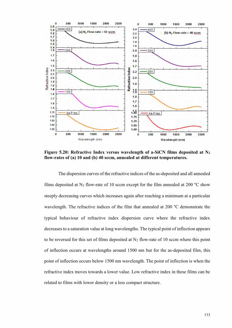
133
Figure 5.20: Refractive Index versus wavelength of a-SiCN films deposited at N2 flow-rates of (a) 10 and (b) 40 sccm, annealed at different temperatures.
The dispersion curves of the refractive indices of the as-deposited and all annealed
films deposited at N2 flow-rate of 10 sccm except for the film annealed at 200 °C show
steeply decreasing curves which increases again after reaching a minimum at a particular
wavelength. The refractive indices of the film that annealed at 200 °C demonstrate the
typical behaviour of refractive index dispersion curve where the refractive index
decreases to a saturation value at long wavelengths. The typical point of inflection appears
to be reversed for this set of films deposited at N2 flow-rate of 10 sccm where this point
of inflection occurs at wavelengths around 1500 nm but for the as-deposited film, this
point of inflection occurs below 1500 nm wavelength. The point of inflection is when the
refractive index moves towards a lower value. Low refractive index in these films can be
related to films with lower density or a less compact structure.
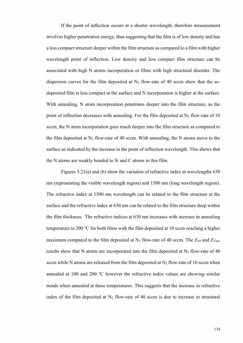
134
If the point of inflection occurs at a shorter wavelength, therefore measurement
involves higher penetration energy, thus suggesting that the film is of low density and has
a less compact structure deeper within the film structure as compared to a film with higher
wavelength point of inflection. Low density and less compact film structure can be
associated with high N atoms incorporation or films with high structural disorder. The
dispersion curves for the film deposited at N2 flow-rate of 40 sccm show that the as-
deposited film is less compact at the surface and N incorporation is higher at the surface.
With annealing, N atom incorporation penetrates deeper into the film structure, as the
point of inflection decreases with annealing. For the film deposited at N2 flow-rate of 10
sccm, the N atom incorporation goes much deeper into the film structure as compared to
the film deposited at N2 flow-rate of 40 sccm. With annealing, the N atoms move to the
surface as indicated by the increase in the point of inflection wavelength. This shows that
the N atoms are weakly bonded to Si and C atoms in this film.
Figures 5.21(a) and (b) show the variation of refractive index at wavelengths 630
nm (representing the visible wavelength region) and 1500 nm (long wavelength region).
The refractive index at 1500 nm wavelength can be related to the film structure at the
surface and the refractive index at 630 nm can be related to the film structure deep within
the film thickness. The refractive indices at 630 nm increases with increase in annealing
temperature to 200 °C for both films with the film deposited at 10 sccm reaching a higher
maximum compared to the film deposited at N2 flow-rate of 40 sccm. The E04 and ETauc
results show that N atoms are incorporated into the film deposited at N2 flow-rate of 40
sccm while N atoms are released from the film deposited at N2 flow-rate of 10 sccm when
annealed at 100 and 200 °C however the refractive index values are showing similar
trends when annealed at these temperatures. This suggests that the increase in refractive
index of the film deposited at N2 flow-rate of 40 sccm is due to increase in structural
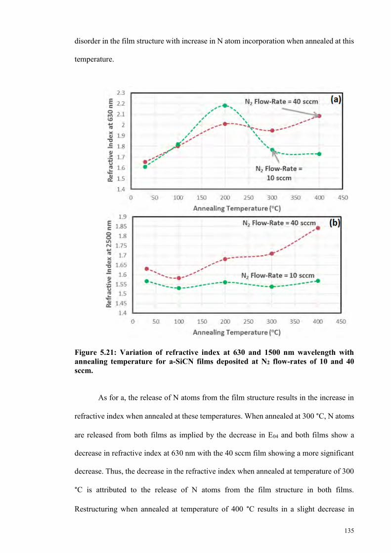
135
disorder in the film structure with increase in N atom incorporation when annealed at this
temperature.
Figure 5.21: Variation of refractive index at 630 and 1500 nm wavelength with annealing temperature for a-SiCN films deposited at N2 flow-rates of 10 and 40 sccm.
As for a, the release of N atoms from the film structure results in the increase in
refractive index when annealed at these temperatures. When annealed at 300 °C, N atoms
are released from both films as implied by the decrease in E04 and both films show a
decrease in refractive index at 630 nm with the 40 sccm film showing a more significant
decrease. Thus, the decrease in the refractive index when annealed at temperature of 300
°C is attributed to the release of N atoms from the film structure in both films.
Restructuring when annealed at temperature of 400 °C results in a slight decrease in
136
refractive index for the 10 sccm film but there is increment for the 40 sccm film. The
slight decrease in the refractive index of the film deposited at N2 flow-rate of 10 sccm can
be due to the effect of restructuring where structural order in the film is improved.
However, the refractive index of the 40 sccm film increases again when annealed at 400
°C suggesting the broken bonds maybe from Si-C-N bonds and restructuring results in
the formation of a-Si-C phases which have a higher refractive index compared to a
dominant a-SiCN phase.
The refractive index of the film deposited at N2 flow-rate of 40 sccm in the long
wavelength region is much higher for the film deposited at 40 sccm compared to the film
deposited at 10 sccm. Thus, this indicates that the surface of the 40 sccm is more compact
compared to the surface of the 10 sccm film even when annealed. N atom incorporation
is higher at the surface of the 10 sccm film. The film deposited at N2 flow-rate of 40 sccm
shows a continuously increasing trend of the refractive index with increase in annealing
temperature while the refractive index in the long wavelength region of the film deposited
at N2 flow-rate of 10 sccm does not change much with increase in annealing temperature.
N atoms are released from the surface of the 40 sccm film continuously with increase in
annealing temperature. Annealing up to 400 °C does not change the refractive index of
the film in the long wavelength region because the N atoms are mostly embedded deep
into the bulk of the film structure especially when annealed at 300 and 400 °C as indicated
by low refractive index at 630 sccm.
Thus, annealing at low temperatures of 100 and 200 °C is found to release N atoms
from weak bonds in the bulk of the film deposited at low N2 flow-rate resulting in the
increase in the refractive index of the film in the bulk. These N atoms migrate to the
surface and restructuring removes defects from the bulk resulting in the decrease in
refractive index at 630 nm wavelength. The refractive index at 1500 nm wavelength does
not show much change when annealed because the diffusion and release of N atoms and
137
restructuring are active in the bulk of the film only. On the other hand, annealing at low
temperatures of 100 and 200 °C incorporate N atoms into the film structure in the bulk
resulting in increase in structural disorder in the film deposited at high N2 flow-rate
resulting in the increase in the refractive index of the film in the bulk. These N atoms are
released from bonds in the bulk leaving defects and structural disorders of dangling bonds
and vacancies thus refractive index at 630 nm wavelength continues to increase. The N
atoms then migrate to the surface and are evolved from the film structure resulting in the
decrease in refractive index at 630 nm wavelength and increase in the refractive index at
1500 nm wavelength when annealed at high annealing temperatures of 400 and 500 °C.
5.7 Summary
The first part of this chapter was focused on studying the aging effects on the
structural properties of films deposited by PECVD from the discharge of SiH4 and CH4
with and without N2. In the second part of this chapter, the effects of annealing on the
structural and optical properties deposited at N2 flow-rates of 10 and 40 sccm representing
low and high N2 flow-rate deposition respectively were studied. Some interesting results
were obtained for consideration when using a-SiCN films in various applications.
Aging of film deposited from the discharge of SiH4 and CH4 without N2 showed
that the Si-H and C-H bonds in the film are weak and O atoms from the environment
easily diffuse into the Si-H and C-H bonds forming O-H bonds in the film structure with
time. The Si-C bonds formed are strong and H atoms released from Si-H and C-H bonds
are bonded to free bonds on the Si and C atoms forming Si-CH3 bonds. Aging in of films
deposited from SiH4 and CH4 with N2 showed that Si-H, OH, C-H and N-H vibrational
bonds are stable with aging with incorporation of N atoms into the structure of the films.
The Si-C-N and C-N bonds increase while Si-N bonds decreases with aging in these films.
138
The Si-C bonds deposited with N2 flow-rates of 10 and 40 sccm are very stable with
aging.
The graphitic grains in the a-SiC:H films are significantly reduced with ageing as
reflected by the significant decrease in the intensity of the D and G bands for the aged
films. The relaxed form of C-N bonds in the form of T band C-N bonds are present in
aged film deposited with N2 flow-rate. The strong N ion bombardment during the growth
process had caused the formation of weak Si-N bonds. Upon aging N atoms are
diassociated from Si-N bonds and further migrate towards free C atoms to form larger
number of these strong C-N bonds. Incorporation of the N atoms into the graphitic phase
of the film structure improves the structural order especially for the film deposited at 40
sccm. N2 flow-rate of 40 sccm produces the optimum N ion bombardment effects to form
a-SiCN:H films which does not deteriorate with aging in atmospheric environments. The
high N ion bombardments during growth of the film deposited at N2 flow-rate of 10 sccm
results in unstable bonds which result in increase in structural disorder when aged in
atmospheric environment.
The highly defective structure of the film deposited with high N ion bombardment
showed that annealing at low temperatures of 100 and 200 °C improves the film structure
due to removal of defects such as dangling bonds and vacancies which induced the
increase in the number of C-N and Si-C bonds in this film structure. Annealing at
temperature of 300 °C resulted in the formation of a dominant a-SiCN in the film
structure. Annealing of films deposited with low N ion bombardment at temperatures of
300 °C and above increased the number of phases in the film structure. Low temperature
annealing improved the film structure due to the out-diffusion process of N atoms from
weak Si-N and C-N bonds and migration of these N atoms to form strong bonds Si-N and
C-N bonds and restructuring of dangling bonds to form new Si-C bonds.
139
The graphitic phase is more prominent in the film grown at low N2 flow-rate
especially when annealed at temperature of 100 °C. The C-N bonds in the graphitic phase
are weak and easily release N atoms when annealed. The graphitic phase disappears in
the films annealed at high temperatures above 300 °C. Increase in N incorporation leads
to an increase in the number of phases and this increases in disorder in the film structure.
Increase in N atom incorporation in the film structure increases E04 and increase in
structural disorder in the film structure decreases ETauc. In this work, it was successfully
shown that the refractive index at 630 and 1500 nm can be used as a gauge to relate this
parameter to the structural properties of the film in the bulk and at surface of the film
respectively. Increase in N incorporation which results in increase in the structural
disorder of the film structure result in an increase in refractive index but if otherwise that
is improvement in structural disorder decreases the refractive index.
140
CHAPTER 6: CONCLUSION AND SUGGESTION FOR FUTURE WORKS
6.1 Conclusions
In this work, plasma enhanced chemical vapour deposition (PECVD), which is
a popular technique used in the growth of many Si based thin films has been used to grow
hydrogenated amorphous silicon carbide (a-SiCN:H) thin films. This material indeed
combines excellent properties of SiC, Si3N4 and C3N4 compounds, thus, making it a
promising material for various applications such as passivation layers for crystalline solar
cell, light emitting diodes, opto-electronic devices and biomedical applications.
6.2 Summary of Overall Finding
The significance of findings in current study which are based the objectives that
had been outlined in Chapter 1 can be highlighted as below:
The films grown on both c-Si and glass substrates were multi-phase in structure
with dominant components that composed of a-SiCN:H, a-SiC:H and a-C:H phases and
these multi-phase was found to affect the microstructure, optical and photoluminescence
properties of the films. N2 flow-rate was shown to have great influence on the elemental
composition, bonding and photoluminescence properties of a-SiCN films that deposited
by PECVD on c-Si substrates. PL and optical properties investigated on films grown on
glass substrates also showed dependence on the N2 flow-rate.
The incorporation of nitrogen atoms into the film structure was obviously
influenced by the energy of nitrogen atoms bombarding on the growth sites. The decrease
in the growth rate of the films with increase in N2 flow-rate can be attributed to the higher
energy of bombardments by N atom towards the growth sites and subsequently promote
the incorporation of N atoms into the structure of film and thus caused the formation of a
more compact and homogeneous film structure. The lower energy reactive N atom
141
bombardments on the growth sites at high N2 flow-rates also was more favourable in the
formation of a-SiCN:H phases in the film structure as reflected by the AES and FTIR
analysis, where at high N2 flow-rates, most of the N atoms were bonded to either the Si
and C atoms to form Si-C-N, C-Si-N, Si-C=N or Si-CN bonds.
The higher impact energy at low N2 flow-rates reduced the presence of a-C:H
phase as the sp2-C clusters in the film structure were shown to decrease from the analysis
done the Raman spectra of the films. The decrease in impact energy and increase in the
number of reactive N atoms at the growth sites at high N2 flow-rates increased the a-C:H
phase in the film structure due to reduced residual compressive stress on the sp2-C
clusters. This was also shown to increase the size of the sp2-C clusters in the a-C:H phases
in the film structure. The decrease in the refractive index of the films at low N2 flow-rate
was shown to be consistent with the decrease in the a-C:H phase in the films as result of
the decrease in N atom incorporation in the film structure.
In this work, the energy values extracted from the Tauc’s plot, ETauc and energy at
absorption coefficient 104 cm-1, E04 tail factor (Etail = E04 - ETauc) were obtained from the
films deposited on glass substrates. N2 flow-rate produces significant effects on the E04
and Etail values. E04 was shown to be dependent on the dominant phase present in the
film structure. And increase in Etail with increase in N2 flow-rate was shown to be due to
the increase in the number of phases in the film structure.
The broad PL emission spectra of the films ranging from 400 to 750 nm confirmed
that the a-SiCN:H films are multi-phase in structure. The PL emission properties are
substrate dependent with higher emission intensity from the films on c-Si substrates but
and suppression of some emission peaks were from the films on glass substrate. PL
emission analysis showed that the origin of the most dominant PL emission from the film
deposited without N2 on c-Si substrates and with and without N2 were from recombination
within tail states of a-C:H phase in the films. Films deposited on c-Si substrates with N2
142
produced PL emission with origin from recombination within tail states of a-CN:H and
a-SiCN:H phases in the film structure. Thus, significant N incorporation into the film
structure reduced the a-C:H phase in the film structure and increased a-CN:H and a-
SiCN:H phases. It was therefore established that N incorporation is low in the films
deposited on glass substrates.
The Si-H, OH, C-H and N-H bonds are stable with ageing with N incorporation
into the film structure. These bonds were unstable in the film deposited from the discharge
of SiH4 and CH4 without N2. O atoms from the environment easily diffused into the Si-H
and C-H bonds forming O-H bonds. The Si-C bonds in this film formed were
demonstrated to be strong and H atoms released from Si-H and C-H migrated to the free
bonds on the Si and C atoms forming Si-CH3 bonds. Ageing in of films deposited from
SiH4 and CH4 with the presence of N2 had caused the increment in the concentration of
Si-C-N and C-N bonds but decreased Si-N bonds concentration in the films. This is the
result of migration of N atoms from broken Si-N bonds towards free C atoms to form the
relaxed form of C-N bonds in the form of T band C-N bonds which was more stable.
N2 flow-rate of 40 sccm produces the optimum N ion bombardment effects to
form a-SiCN:H films, which showed minimum deterioration with ageing in atmospheric
environments. High energetic N ion bombardments during the growth of the film at lower
N2 flow-rate has resulted in unstable bonds which induced structural disorders when aged
in atmospheric environment.
The highly defective structure of the film deposited with high N ion bombardment
showed that annealing at low temperatures of 100 and 200 °C improved the film structure
with increase in concentration of C-N and Si-C bonds in this film structure. Low
temperature annealing improved the film structure due to the out-diffusion process of N
atoms from weak Si-N and C-N bonds and migration of these N atoms to form strong
bonds Si-N and C-N bonds and restructuring of dangling bonds to form new Si-C bonds.
143
Annealing of films deposited with low N ion bombardment at temperatures of 300
°C and above increased the number of phases in the film structure. The graphitic phases
were more prominent in the film grown at low N2 flow-rates. The graphitic phase
disappears in the films annealed at high temperatures above 300 °C. Increase in N
incorporation leads to an increment in the number of phases and this increased disorder
in the film structure.
6.3 Significant of Current Study
The discharge of N2 at different flow-rates mixed in silane (SiH4) and methane
(CH4) at fixed flow-rates in current study has results in the growth of multi-phase
structured films with unique structural, optical and photoluminescence properties and all
these properties are highly governed by N2 flow-rate. This kind of output is not new for
Si based thin films but surprisingly not much has been reported on the growth of a-
SiCN:H thin films by PECVD using N2 as the source for N atom incorporation into the
film structure. Most work uses ammonia (NH3) gas for this purpose since it is very
reactive as compared to N2. Comparatively, N2 is easier to handle, cheaper and not
harmful to the environment. Therefore, the findings from this research have contributed
in terms of cost effectiveness and more environmentally as well as assist in the
development of user-friendly synthesis scheme. SiH4 is a highly toxic gas but the flow-
rate used during the growth process is very low and the synthesis process is greatly eased
when the synthesis is carried out along with N2.
Since N2 is used in the growth of a-SiCN films in this work, the aspects on the
degradation of films due to ageing and thermal effects are crucial in the applications of
this material in devices. In this work, ageing and annealing are shown to produce
significant effects on the structure and optical properties of the films and the effects are
shown to be dependent on the flow-rate of N2 gas used during the growth process.
144
6.4 Suggestions for Future Works
In order to expand current work and for enabling better understanding of the
properties of a-SiCN:H thin films that deposited by conventional PECVD, which is an
established technique that can feasibly maneuvering the structural, electronic and optical
properties of Si based thin films, there are still plenty of rooms needed to be addressed
and below suggestion is proposed for future works:
a) Similar investigations on the properties of a-SiCN:H film deposited by PECVD
with respect to other deposition parameters like RF power, SiH4 to CH4 flow-rate
at fixed N2 flow-rate, deposition pressure and substrate temperature and the effects
of ageing and annealing temperature on these films.
b) Ageing issues for the deposited film must be better understood. Approaches for
reducing or controlling the effects of ageing need to be further studied. Therefore,
more accurate analysis on the issues of ageing like higher frequency of
measurements (say 1 measurement / week) and a longer period of observation (say
in a span of 6 months) should be carried out.
c) To grow a-SiCN:H films by Plasma-Assisted Hot-Filament CVD since the hot-
filament can induce higher dissociation of silane and the plasma can enhance
dissociation of methane and N2 and study ageing and annealing effects on films
deposited at various varied growth parameters.
d) Since one potential application of the film is to increase solar cell performance
which involves light exposure, effects of degradation of film due to light
illumination also need to be studied.
e) Investigations on the origin PL of multi-phase structured material. Effects of
annealing and ageing on PL emission of the films deposited at different growth
parameters maybe useful in achieving this.
145
f) The correlation between the PL efficiency and the optical parameters
which include optical energy band gaps determined by the Tauc plot and
ETauc energy at absorption coefficient of 104 cm-1, E04 , dispersion energy,
ED and single oscillator energy, Eo.
146
REFERENCES
Afanasyev-Charkin, I., & Nastasi, M. (2004). Hard Si–N–C coatings produced by pulsed glow discharge deposition. Surface and Coatings Technology, 186(1), 108-111.
Ambrosone, G., Coscia, U., Ferrero, S., Giorgis, F., Mandracci, P., & Pirri, C. (2002).
Structural and optical properties of hydrogenated amorphous silicon-carbon alloys grown by plasmaenhanced chemical vapour deposition at various RF powers. Philosophical Magazine B, 82(1), 35-46.
Aoi, Y., Ono, K., Sakurada, K., Kamijo, E., Sasaki, M., & Sakayama, K. (2001). Effects
of heat treatment on structure of amorphous CNx thin films by pulsed laser deposition. Thin Solid Films, 389(1), 62-67.
Arya, R., & Carlson, D. (2002). Amorphous silicon PV module manufacturing at BP
solar. Progress in Photovoltaics: Research and Applications, 10(2), 69-76.
Awad, Y., El Khakani, M., Scarlete, M., Aktik, C., Smirani, R., Camiré, N., . . . Mouine, J. (2010). Structural analysis of silicon carbon nitride films prepared by vapor transport-chemical vapor deposition. Journal of Applied Physics, 107(3), 033517.
Barrett, D. L., McHugh, J. P., Hobgood, H. M., Hopkins, R. H., McMullin, P. G., Clarke,
R. C., & Choyke, W. J. (1993). Growth of large SiC single crystals. Journal of Crystal Growth, 128(1), 358-362.
Bendeddouche, A., Berjoan, R., Beche, E., Merle-Mejean, T., Schamm, S., Serin, V., . . .
Hillel, R. (1997). Structural characterization of amorphous SiCxNy chemical vapor deposited coatings. Journal of Applied Physics, 81, 6147-6154.
Bendeddouche, A., R. B., E. Beche, and R. Hillel, . (1999). Hardness and stiffness of
amorphous SiCxNy chemical vapor deposited. Surface and Coatings Technology, 111, 184−190.
Betranhandy, E., Capou, L., Matar, S. F., & El-Kfoury, C. (2004). First principles search
of hard materials within the SiCN ternary system. Solid State Sciences, 6(4), 315-323.
Bulou, S., Le Brizoual, L., Miska, P., De Poucques, L., Hugon, R., Belmahi, M., &
Bougdira, J. (2011). The influence of CH 4 addition on composition, structure and optical characteristics of SiCN thin films deposited in a CH 4/N 2/Ar/hexamethyldisilazane microwave plasma. Thin Solid Films, 520(1), 245-250.
Cao, Z. (2002). Plasma enhanced deposition of silicon carbonitride thin films and
property characterization. Diamond and Related Materials, 11(1), 16-21. Catherine, Y., Zamouche, A., Bullot, J., & Gauthier, M. (1983). Ion bombardment effects
in plasma deposition of hydrogenated amorphous silicon carbide films: a comparative study of DC and RF discharges. Thin Solid Films, 109(2), 145-158.
Chang, C. (1975). General formalism for quantitative Auger analysis. Surface Science, 48(1), 9-21.
147
Chang, Y., Hsieh, H., Pong, W., Tsai, M.-H., Lee, K., Dann, T., . . . Su, W. (1998). Electronic and atomic structures of the Si-CN thin film by X-ray-absorption spectroscopy and theoretical calculations. Physical Review B, 58(14), 9018.
Charles, C., Martin, N., Devel, M., Ollitrault, J., & Billard, A. (2013). Correlation between structural and optical properties of WO3 thin films sputter deposited by glancing angle deposition. Thin Solid Films, 534, 275-281.
Chattopadhyay, S., Chen, L., Wu, C., Chen, K., Wu, J., Chen, Y., . . . Hess, P. (2001).
Thermal diffusivity in amorphous silicon carbon nitride thin films by the traveling wave technique. Applied Physics Letters, 79(3), 332-334.
Chen, C., Huang, C., Lin, Y., Chen, L., & Chen, K. (2005). The affinity of Si–N and Si–
C bonding in amorphous silicon carbon nitride (a-SiCN) thin film. Diamond and Related Materials, 14(3), 1126-1130.
Chen, C., Lee, M.-H., Chen, L., & Chen, K. (2004). Structural and electronic properties
of wide band gap silicon carbon nitride materials—a first-principles study. Diamond and Related Materials, 13(4), 1158-1165.
Chen, L., Chen, C., Wei, S., Bhusari, D., Chen, K., Chen, Y., . . . Huang, Y. (1998).
Crystalline silicon carbon nitride: A wide band gap semiconductor. Applied Physics Letters, 72(19), 2463-2465.
Chen, L., Wu, C., Wu, J.-J., & Chen, K. (2000). Growth, characterization, and properties
of carbon nitride with and without silicon addition. International Journal of Modern Physics B, 14(2&3), 333-348.
Chen, Z., Lin, H., Zhou, J., Ma, Z., & Xie, E. (2009). IR studies of SiCN films deposited
by RF sputtering method. Journal of Alloys and Compounds, 487(1), 531-536.
Cheng, W. J., Jiang, J. C., Zhang, Y., Shen, D. Z., & Zhu, H. S. (2005). Field emission
properties of nanocrystalline and amorphous silicon carbon nitride prepared from microwave plasma chemical vapor deposition. Paper presented at the Materials Science Forum.
Chu, V., Conde, J., Jarego, J., Brogueira, P., Rodriguez, J., Barradas, N., & Soares, J.
(1995). Transport and photoluminescence of hydrogenated amorphous silicon–carbon alloys. Journal of Applied Physics, 78(5), 3164-3173.
Conde, J., Chu, V., Da Silva, M., Kling, A., Dai, Z., Soares, J., . . . Giorgis, F. (1999).
Optoelectronic and structural properties of amorphous silicon–carbon alloys deposited by low-power electron-cyclotron resonance plasma-enhanced chemical-vapor deposition. Journal of Applied Physics, 85(6), 3327-3338.
Cui, L., Wang, Q., Xu, B., Yu, D., Liu, Z., Tian, Y., & He, J. (2013). Prediction of novel
SiCN compounds: first-principles calculations. The Journal of Physical Chemistry C, 117(42), 21943-21948.
Davis, J. R. (1992). ASM materials engineering dictionary: ASM international.
148
Della Sala, D., Coluzza, C., Fortunato, G., & Evangelisti, F. (1985a). Infrared and optical study of a-SiN alloys. Journal of Non-Crystalline Solids, 77, 933-936.
Della Sala, D., Fiorini, P., Frova, A., Gregori, A., Skumanich, A., & Amer, N. (1985b).
Gap state spectroscopy in a-SixC1− x: H alloys. Journal of Non-Crystalline Solids, 77, 853-856.
Demichelis, F., Schreiter, S., & Tagliaferro, A. (1995). Photoluminescence in a-C: H
films. Physical Review B, 51(4), 2143. Dunn, K. (2011). Luminescent SiCxNy thin films deposited by ICP-CVD (Doctoral
dissertation), McMaster University. Dutta, R., Banerjee, P., & Mitra, S. (1982). Effect of hydrogenation on the electrical
conductivity of amorphous silicon carbide. Solid State Communications, 42(3), 219-222.
Emeleus, H., & Stewart, K. (1935). 281. The oxidation of the silicon hydrides. Part I.
Journal of the Chemical Society (Resumed), 1182-1189. Ermakova, E., Rumyantsev, Y., Shugurov, A., Panin, A., & Kosinova, M. (2015).
PECVD synthesis, optical and mechanical properties of silicon carbon nitride films. Applied Surface Science, 339, 102-108.
Feenstra, K., Schropp, R., & Van der Weg, W. (1999). Deposition of amorphous silicon
films by hot-wire chemical vapor deposition. Journal of Applied Physics, 85(9), 6843-6852.
Fernandez-Ramos, C., Sanchez-Lopez, J., Rojas, T., & Fernandez, A. (2003). Structural
modifications of silicon-doped carbon nitride films during post-deposition annealing. Diamond and Related Materials, 12(3), 1055-1060.
Fernández-Ramos, C., Sayagués, M., Rojas, T., Alcalá, M., Real, C., & Fernández, A.
(2000). Study of the thermal stability of carbon nitride thin films prepared by reactive magnetron sputtering. Diamond and Related Materials, 9(2), 212-218.
Ferrari, A. C., & Robertson, J. (2000). Interpretation of Raman spectra of disordered and amorphous carbon. Physical review B, 61(20), 14095.
Ferreira, I., Cabrita, A., Fortunato, E., & Martins, R. (2002). Composition and structure
of silicon-carbide alloys obtained by hot wire and hot wire plasma assisted techniques. Vacuum, 64(3), 261-266.
Fraga, M. A., Maciel, H. S., Massi, M., & Pessoa, R. S. (2012). Applications of SiC-based
thin films in electronic and MEMS devices: INTECH Open Access Publisher. Gillespie, D. (1994). Impatience: Jurij Trifonov and the Roots of Revolution. Russian
Literature, 36(4), 435-452. Giorgis, F., Pirri, C., & Tresso, E. (1997). Structural properties of a-Si1−xNx:H films
grown by plasma enhanced chemical vapour deposition by SiH4+NH3+H2 gas mixtures. Thin Solid Films, 307(1), 298-305.
149
Goodman, N. B. (1982). Effect of annealing and light exposure on the field-effect density
of states in glow-discharge a-Si: H. Philosophical Magazine B, 45(4), 407-434. Green, M. A., Emery, K., Hishikawa, Y., Warta, W., & Dunlop, E. D. (2015). Solar cell
efficiency tables (Version 45). Progress in Photovoltaics: Research and Applications, 23(1), 1-9.
Güneş, M., Johanson, R., Kasap, S., Finger, F., & Lambertz, A. (2010). The effect of
aging on the dark con-ductivity and 1/f noise in hydrogen-ated microcrystalline silicon thin films. Phys. Status Solidi C, 7(3-4), 658-661.
Guthy, C., Singh, A., Tanha, J., & Evoy, S. (2010). SiCN nanomechanical resonators for
array-based biosensor applications. NSTI Nanotechnology, 3, 4-6. Hamadi, O. A., Yahia, K. Z., & Jassim, O. N. (2005). Properties of Inclined Silicon
Carbide Thin Films Deposited by Vacuum Thermal Evaporation. JSTS: Journal of Semiconductor Technology and Science, 5(3), 182-186.
Hellgren, N., Johansson, M. P., Broitman, E., Hultman, L., & Sundgren, J.-E. (1999).
Role of nitrogen in the formation of hard and elastic CNx thin films by reactive magnetron sputtering. Physical Review B, 59(7), 5162.
Hellgren, N., Lin, N., Broitman, E., Serin, V., Grillo, S. E., Twesten, R., . . . Sundgren,
J.-E. (2001). Thermal stability of carbon nitride thin films. Journal of Materials Research, 16(11), 3188-3201.
Hoffmann, P., Fainer, N., Kosinova, M., Baake, O., & Ensinger, W. (2011). Compilation
on synthesis, characterization and properties of silicon and boron carbonitride films Silicon Carbide-Materials, Processing and Applications in Electronic Devices: InTech
Huang, X., Ma, T., Xu, J., Li, Z., Mei, J., Li, X., . . . Chen, K. (2003). Visible
electroluminescence from amorphous hydrogenated silicon carbide prepared by using organic carbon source. Diamond and Related Materials, 12(10), 1932-1935.
Ibrahim, A., & Al-Ani, S. (1994). Models of optical absorption in amorphous semiconductors at the absorption edge—a review and re-evaluation. Czechoslovak Journal of Physics, 44(8), 785-797.
Ivashchenko, V., Ivashchenko, L., Srynsckyy, P., & Grishnova, L. (2008). Ab initio
simulations of liquid and amorphous SIC and SICN Carbon Nanomaterials in Clean Energy Hydrogen Systems (pp. 857-862): Springer
Jenkins, F.A. and White, H.E. (1981). Fundamentals of Optics. McGraw-Hill, Inc. . Kabir, M., Amin, N., Zaharim, A., Sopian, K., Perlovsky, L., Dionysiou, D., . . . Jaberg,
H. (2009). Effect of Energy Bandgap of the Amorphous Silicon Carbide(A-Sic: H) Layers On A-Si Multijuntion Solar Cells from Numerical Analysis. Paper presented at the WSEAS International Conference. Proceedings. Mathematics and Computers in Science and Engineering.
150
Kaltenpoth, G., Siebert, W., Stubhan, F., Wang, X., & Luo, L. (2002). Moisture barrier properties of plasma enhanced chemical vapor deposited SiCxNy films on polyethylene naphthalate sheets and epoxy molding compound. Surface and Coatings Technology, 161(1), 96-101.
Kawamoto, H. (2002). INVITED PAPER: The History of Liquid-Crystal Displays.
Proceedings of the IEEE, 90, 460-500. Kawamura, T. (1965). Silicon carbide crystals grown in nitrogen atmosphere.
Mineralogical Journal, 4(5), 333-355. Kim, D. S., Kang, M. H., Rohatgi, A., Davies, M., Hong, J., Jakubowska-Okoniewski,
G., & Ebong, A. (2008). Silicon carbonitride antireflective coating: Google Patents.
Konuma, M. (1992). Film Deposition by Plasma Technology: Springer Verlag, New
York. Kozak, A., Ivashchenko, V., Porada, O., Ivashchenko, L., Sinelnichenko, O., Dub, S., . .
. Tolmacheva, G. (2015). Effect of the nitrogen flow on the properties of Si-CN amorphous thin films produced by magnetron sputtering. Journal of Superhard Materials, 37(5), 300-309.
Krimmel, E. F., Hezel, R., Nohl, U., & Bohrer, R. (1991). Silicon Nitride in Light-
Emitting Diodes (LEDs), Lasers and Displays Si Silicon (pp. 263-269): Springer Kruangam, D., Endo, T., Guang-Pu, W., Nonomura, S., Okamoto, H., & Hamakawa, Y.
(1985). A study of visible-light injection-electroluminescence in a-SiC/pin diode. Journal of Non-Crystalline Solids, 77, 1429-1432.
Le Comber, P., Spear, W., & Ghaith, A. (1979). Amorphous-silicon field-effect device
and possible application. Electronics Letters, 6(15), 179-181. Lee, M.-S., & Bent, S. F. (2000). Temperature effects in the hot wire chemical vapor
deposition of amorphous hydrogenated silicon carbon alloy. Journal of Applied Physics, 87(9), 4600-4610.
Limmanee, A., Otsubo, M., Sugiura, T., Sato, T., Miyajima, S., Yamada, A., & Konagai,
M. (2008). Effect of thermal annealing on the properties of a-SiCN:H films by hot wire chemical vapor deposition using hexamethyldisilazane. Thin Solid Films, 516(5), 652-655.
Liu, Y., Yoon, S., Ahn, J., & Milne, W. (1996). Effect of hydrogen dilution on the
deposition of carbon-rich a-SiC: H films by the electron cyclotron resonance method. Materials Science and Engineering: B, 39(3), 188-194.
Lo, H., Wu, J., Wen, C., Wong, T., Lin, S., Chen, K., & Chen, L. (2001). Bonding
characterization and nano-indentation study of the amorphous SiCxNy films with and without hydrogen incorporation. Diamond and Related Materials, 10(9), 1916-1920.
151
Lowther, J. (1999). Structural stability of some possible phases of SiC2N4. Physical Review B, 60(17), 11943.
Lu, Y., Ren, Z., Song, W., Chan, D., Low, T., Gamani, K., . . . Li, K. (1998). Studies of
carbon nitride thin films synthesized by KrF excimer laser ablation of graphite in a nitrogen atmosphere. Journal of Applied Physics, 84(5), 2909-2912.
Manifacier, J., Gasiot, J., & Fillard, J. (1976). A simple method for the determination of
the optical constants n, k and the thickness of a weakly absorbing thin film. Journal of Physics E: Scientific Instruments, 9(11), 1002.
Matsumura, H., & Ihara, H. (1988). Catalytic chemical vapor deposition method to
prepare high quality hydro‐fluorinated amorphous silicon. Journal of Applied Physics, 64(11), 6505-6509.
Mihailescu, I., Gyorgy, E., Alexandrescu, R., Luches, A., Perrone, A., Ghica, C., . . .
Chumash, V. (1998). Optical studies of carbon nitride thin films deposited by reactive pulsed laser ablation of a graphite target in low pressure ammonia. Thin Solid Films, 323(1), 72-78.
Mort, J., & Jansen, F. (1986). Plasma-deposited thin films: CRC Press Inc.,Boca Raton,
FL. Niemann, J., & Bauhofer, W. (1999). Properties of a-Si1−xCx:H thin films deposited from
the organosilane Triethylsilane. Thin Solid Films, 352(1), 249-258. Noh, S., Fu, X., Chen, L., & Mehregany, M. (2007). A study of electrical properties and
microstructure of nitrogen-doped poly-SiC films deposited by LPCVD. Sensors and Actuators A: Physical, 136(2), 613-617.
Park, M., Teng, C., Sakhrani, V., McLaurin, M., Kolbas, R., Sanwald, R., . . . Cuomo, J.
(2001). Optical characterization of wide band gap amorphous semiconductors (a-Si: C: H): Effect of hydrogen dilution. Journal of Applied Physics, 89(2), 1130-1137.
Peng, G., Jun, X., Wan-Yu, D., & Chuang, D. (2009). Ultra-Thin Silicon Carbon Nitride
Film: a Promising Protective Coating for Read/Write Heads in Magnetic Storage Devices. Chinese Physics Letters, 26(6), 065203.
Peng, Y., Zhou, J., Zhao, B., Tan, X., & Zhang, Z. (2011). Effect of annealing temperature
and composition on photoluminescence properties of magnetron sputtered SiCN films. Thin Solid Films, 519(7), 2083-2086.
Perný, M., Mikolášek, M., Šály, V., Huran, J., & Országh, J. (2012). Current transport
mechanisms of amorphous n-doped silicon carbide/crystalline silicon heterostructure: Impact of nitrogen dopation. Paper presented at the 2012 35th International Spring Seminar on Electronics Technology.
Perrin, J., Leroy, O., & Bordage, M. (1996). Cross‐Sections, Rate Constants and Transport Coefficients in Silane Plasma Chemistry. Contributions to Plasma Physics, 36(1), 3-49.
152
Persheyev, S., Smirnov, V., O’Neill, K., Reynolds, S., & Rose, M. (2005). Atmospheric adsorption effects in hot-wire chemical-vapor-deposition microcrystalline silicon films with different electrode configurations. Semiconductors, 39(3), 343-346.
Peter, S., Bernütz, S., Berg, S., & Richter, F. (2013). FTIR analysis of a-SiCN:H films deposited by PECVD. Vacuum, 98, 81-87.
Poitevin, J., Lemperiere, G., & Tardy, J. (1982). Influence of substrate bias on the
composition, structure and electrical properties of reactively DC-sputtered TiN films. Thin Solid Films, 97(1), 69-77.
Porada, A., Kozak, A., Ivashchenko, L., Ivashchenko, V., & Tomila, T. (2013). Effect of
Added Nitrogen on Properties of SiCN Films Prepared by PECVD Using Hexamethyldisilazane. Paper presented at the Proceedings of the International Conference Nanomaterials: Applications and Properties.
Rabeh, M. B., & Kanzari, M. (2011). Optical constants of Zn-doped CuInS2 thin films.
Thin Solid Films, 519(21), 7288-7291. Rabeh, M. B., Zribi, M., Kanzari, M., & Rezig, B. (2005). Structural and optical
characterization of Sn incorporation in CuInS2 thin films grown by vacuum evaporation method. Materials Letters, 59(24), 3164-3168.
Rahman, M. M., & Furukawa, S. (1984). Preparation and electrical properties of an
amorphous SiC/crystalline Si p+n heterostructure. Japanese Journal of Applied Physics, 23(5R), 515.
Rill, M. S., Plet, C., Thiel, M., Staude, I., Von Freymann, G., Linden, S., & Wegener, M.
(2008). Photonic metamaterials by direct laser writing and silver chemical vapour deposition. Nature Materials, 7(7), 543.
Sachdev, H., & Scheid, P. (2001). Formation of silicon carbide and silicon carbonitride
by RF-plasma CVD. Diamond and Related Materials, 10(3), 1160-1164. Saito, N. & Nakaaki, I. (2001). Optical,electrical and structural properties of amorphous
SiCN:H films prepared by RF glow discharge decomposition. Applied Surface Science, 169-170, 468-471.
Saito, N., Yamada, T., Yamaguchi, T., Nakaaki, I., & Tanaka, N. (1985). Structural,
optical and electronic properties of amorphous SiC:H alloys prepared by magnetron sputtering of silicon in methane-argon gas mixtures. Philosophical Magazine B, 52(5), 987-995.
Saloum, S., & Alkhaled, B. (2011). Structural, optical and electrical properties of plasma
deposited thin films from hexamethyldisilazane compound. Acta Physica Polonica A, 119(3), 369-373.
Sambandam, S. N., Bethala, B., Sood, D. K., & Bhansali, S. (2005). Evaluation of silicon
nitride as a diffusion barrier for Gd–Si–Ge films on silicon. Surface and Coatings Technology, 200(5), 1335-1340.
153
Schüttauf, J.-W., Modestino, M. A., Chinello, E., Lambelet, D., Delfino, A., Dominé, D., . . . Psaltis, D. (2016). Solar-to-Hydrogen Production at 14.2% Efficiency with Silicon Photovoltaics and Earth-Abundant Electrocatalysts. Journal of The Electrochemical Society, 163(10), F1177-F1181.
Schwan, J., Ulrich, S., Batori, V., Ehrhardt, H., & Silva, S. (1996). Raman spectroscopy
on amorphous carbon films. Journal of Applied Physics, 80(1), 440-447. Shaaban, E., Yahia, I., & El-Metwally, E. (2012). Validity of Swanepoel's method for
calculating the optical constants of thick films. Acta Physica Polonica-Series A General Physics, 121(3), 628.
Sharma, S., Jain, K. K., & Sharma, A. (2015). Solar Cells: In Research and
Applications—A Review. Materials Sciences and Applications, 6(12), 1145.
Smirnov, V., Reynolds, S., Main, C., Finger, F., & Carius, R. (2004). Aging effects in microcrystalline silicon films studied by transient photoconductivity. Journal of Non-Crystalline Solids, 338, 421-424.
Somorjai, G. A., & Li, Y. (2010). Introduction to surface chemistry and catalysis: John
Wiley & Sons. Stapinski, T., & Swatowska, B. (2008). a-Si:C:H and a-Si:N:H thin films obtained by
PECVD for applications in silicon solar cells. Journal of Electronic Materials, 37(6), 905-911.
Sundaram, K., & Alizadeh, J. (2000). Deposition and optical studies of silicon carbide
nitride thin films. Thin Solid Films, 370(1), 151-154. Neethirajan, S., Ono, T. & Masayoshi, E. (2012). Characterization of catalytic chemical
vapor-deposited SiCN thin film coatings. International Nano Letters, 2:4. Swain, B. P. (2006). The analysis of carbon bonding environment in HWCVD deposited
a-SiC:H films by XPS and Raman spectroscopy. Surface and Coatings Technology, 201(3), 1589-1593.
Swain, B. P., & Dusane, R. O. (2006). Multiphase structure of hydrogen diluted a-SiC:H
deposited by HWCVD. Materials Chemistry and Physics, 99(2), 240-246. Swain, B. P., & Dusane, R. O. (2007). Effect of substrate temperature on HWCVD
deposited a-SiC:H film. Materials Letters, 61(25), 4731-4734. Swain, B. P., & Hwang, N. M. (2008). Study of structural and electronic environments of
hydrogenated amorphous silicon carbonitride (a-SiCN: H) films deposited by hot wire chemical vapor deposition. Applied Surface Science, 254(17), 5319-5322.
Swain, B. P., Swain, B. S., & Hwang, N. M. (2014). A comparative chemical network study of HWCVD deposited amorphous silicon and carbon based alloys thin films. Journal of Alloys and Compounds, 588, 343-347.
154
Tabata, A., Kuno, Y., Suzuoki, Y., & Mizutani, T. (1993). Preparation of a-SixC1−x:H films by a separately-excited-plasma CVD method. Journal of Non-Crystalline Solids, 164, 1043-1046.
Tabata, A., Kuno, Y., Suzuoki, Y., & Mizutani, T. (1997). Properties of hydrogenated
amorphous silicon carbide films prepared by a separately excited plasma CVD method. Journal of Physics D: Applied Physics, 30(2), 194.
Tabata, A., Kuroda, M., Mori, M., Mizutani, T., & Suzuoki, Y. (2004). Band gap control
of hydrogenated amorphous silicon carbide films prepared by hot-wire chemical vapor deposition. Journal of Non-Crystalline Solids, 338, 521-524.
Tarrach, F., Ch’hayder, A., Guermazi, H., & Guermazi, S. (2008). Dielectric properties
in aged amorphous silicon oxide thin film. Journal of Alloys and Compounds, 456(1), 425-428.
Tauc, J. (1968). Optical properties and electronic structure of amorphous Ge and Si.
Materials Research Bulletin, 3(1), 37-46. Tomasella, E., Rebib, F., Dubois, M., Cellier, J., & Jacquet, M. (2008). Structural and
optical properties studies of sputtered a-SiCN thin films. Paper presented at the Journal of Physics: Conference Series.
Ullal, H., & Von Roedern, B. (2007). Thin film CIGS and CdTe photovoltaic
technologies: commercialization, critical issues, and applications. Paper presented at the Proceedings of the 22nd European Photovoltaic Solar Energy Conference.
Van Sark, W. (2002). Methods of deposition of hydrogenated amorphous silicon for
device applications. Thin Films and Nanostructures, 30, 1-216. Vassallo, E., Cremona, A., Ghezzi, F., Dellera, F., Laguardia, L., Ambrosone, G., &
Coscia, U. (2006). Structural and optical properties of amorphous hydrogenated silicon carbonitride films produced by PECVD. Applied surface science, 252(22), 7993-8000.
Vetter, M., Martı́, I., Orpella, A., Puigdollers, J., Voz, C., & Alcubilla, R. (2004). IR-
study of a-SiCx: H and a-SiCxNy:H films for c-Si surface passivation. Thin Solid Films, 451, 340-344.
Wang, J., Lu, Y., & Shen, Y. (2010). Effect of nitrogen content on phase configuration,
nanostructure and mechanical behaviors in magnetron sputtered SiCxNy thin films. Applied Surface Science, 256(6), 1955-1960.
Wang, X., Liu, Y., Chen, D., Dong, L., & Chen, C. (2007). Photoluminescence of Si-rich
SiNx films deposited by LPCVD under different conditions. International Journal of Modern Physics B, 21(26), 4583-4592.
Wemple, S., & DiDomenico Jr, M. (1971). Behavior of the electronic dielectric constant
in covalent and ionic materials. Physical Review B, 3(4), 1338.
155
Wiesmann, H., Ghosh, A., McMahon, T., & Strongin, M. (1979). a‐Si:H produced by high‐temperature thermal decomposition of silane. Journal of Applied Physics, 50(5), 3752-3754.
Willander, M., Friesel, M., Wahab, Q.-u., & Straumal, B. (2006). Silicon carbide and
diamond for high temperature device applications. Journal of Materials Science: Materials in Electronics, 17(1), 1-25.
Wrobel, A., Błaszczyk, I., Walkiewicz-Pietrzykowska, A., Tracz, A., Klemberg-Sapieha,
J., Aoki, T., & Hatanaka, Y. (2003). Remote hydrogen–nitrogen plasma chemical vapor deposition from a tetramethyldisilazane source. Part 1. Mechanism of the process, structure and surface morphology of deposited amorphous hydrogenated silicon carbonitride films. Journal of Materials Chemistry, 13(4), 731-737.
Wu, X., Cai, R., Yan, P., Liu, W., & Tian, J. (2002). SiCN thin film prepared at room temperature by RF reactive sputtering. Applied Surface Science, 185(3), 262-266.
Wu, Z., Hong, B., Cheng, K., Zhang, F., Jin, C., Yu, T., & Wu, X. (2014). Structure and photoluminescence properties of SiCN films grown by dual ion beam reactive sputtering deposition. Vacuum, 101, 205-207.
Wydeven, T., & Kawabe, T. (2009). Deposition and characterization of silicon carbon
nitride films prepared by RF-PECVD with capacitive coupling. Paper presented at the Proceedings of the 19th International Symposium on Plasma Chemistry, Bochum, Germany.
Xu, J., Mei, J., Huang, X., Li, W., Li, Z., Li, X., & Chen, K. (2004). The change of
photoluminescence characteristics of amorphous carbon films due to hydrogen dilution. Journal of Non-Crystalline Solids, 338, 481-485.
Xu, L., Zhao, Z., Wang, L.-M., Xu, B., He, J., Liu, Z., & Tian, Y. (2010). Prediction of a
three-dimensional conductive superhard material: diamond-like BC2. The Journal of Physical Chemistry C, 114(51), 22688-22690.
Zhou, F., Yue, B., Wang, X., Wu, X., & Zhuge, L. (2010). Surface roughness, mechanical
properties and bonding structure of silicon carbon nitride films grown by dual ion beam sputtering. Journal of Alloys and Compounds, 492(1), 269-276.
156
LIST OF PUBLICATIONS
Journal (ISI-Cited Publication)
1. Abdul Rahman, M. A., Chiu, W. S., Haw, C. Y., Badaruddin, R., Tehrani, F.
S., Rusop, M., Khiew, P. S., Rahman, S. A. (2017). Multi-phase structured
hydrogenated amorphous silicon carbon nitride thin films grown by plasma
enhanced chemical vapour deposition. Journal of Alloys and Compounds, 721,
70-79.
2. Rahman, M. A. A., Goh, B. T., Chiu, W. S., Haw, C. Y., Mahmood, M. R.,
Khiew, P. S., & Rahman, S. A. (2018). Aging-and thermal-annealing effects on
the vibrational-and microstructural-properties of PECVD grown hydrogenated
amorphous silicon carbon nitride thin films. Vibrational Spectroscopy, 94, 22-30.
Proceeding Paper (ISI-Cited Publication)
1. Rahman, M. A. A., Tong, G. B., Mahmood, M. R., Siong, C. W., Yian, H. C., &
Rahman, S. A. (2016). Effect of Varying Nitrogen Flow Rates on the Optical
Properties of Amorphous-SiCN Thin Films. AIP Conference Proceedings,
1784(1), 040024.
Proceeding
1. Rahman, M. A. A., Tong, G. B., Mahmood, M. R., Siong, C. W., Yian, H. C., &
Rahman, S. A. (2016). Effect of Varying Nitrogen Flow Rates on the Optical
Properties of Amorphous-SiCN Thin Films. 2016 Postgraduate Colloquium in
Faculty of Science and Technology in Universiti Kebangsaan Malaysia from 13-
14 April 2016.
157
158
159