Embed Size (px)
Citation preview
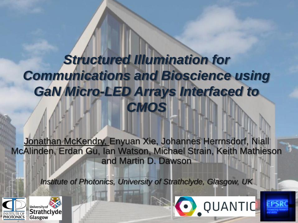
Structured Illumination for
Communications and Bioscience using
GaN Micro-LED Arrays Interfaced to
CMOS
Jonathan McKendry, Enyuan Xie, Johannes Herrnsdorf, Niall McAlinden, Erdan Gu, Ian Watson, Michael Strain, Keith Mathieson
and Martin D. Dawson
Institute of Photonics, University of Strathclyde, Glasgow, UK
• Institute of Photonics overview
• GaN micro-LEDs
• Integration of micro-LEDs and CMOS drivers
• Application #1: “Smart Lighting” indoor positioning
• Application #2: Visible Light Communication
• Application #3: Bioscience & Optogenetics
• Summary and concluding remarks
Overview
ETCMOS, Warsaw, Poland 28th-30th May 2017 2
• Founded in 1995
– Moved to Technology and Innovation Centre in 2015
– > 1000 m2 lab and cleanroom space
– Approximately 50 staff and PhD students
• Research strengths include:
– Diamond photonics
– Semiconductor disc lasers
– GaN micro-LEDs
– Neurophotonics
– Novel photonic materials
Institute of Photonics – an overview
ETCMOS, Warsaw, Poland 28th-30th May 2017 3
GaN micro-LED arrays
ETCMOS, Warsaw, Poland 28th-30th May 2017 4
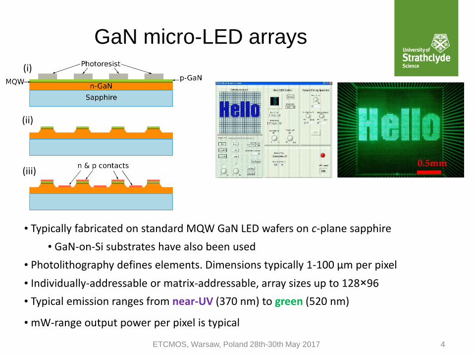
• Typically fabricated on standard MQW GaN LED wafers on c-plane sapphire
• GaN-on-Si substrates have also been used
• Photolithography defines elements. Dimensions typically 1-100 µm per pixel
• Individually-addressable or matrix-addressable, array sizes up to 128×96
• Typical emission ranges from near-UV (370 nm) to green (520 nm)
• mW-range output power per pixel is typical
(i)
(ii)
(iii)
ETCMOS, Warsaw, Poland 28th-30th May 2017 5
CMOS drivers & integration
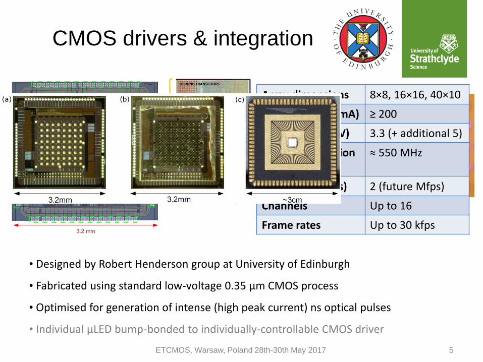
Array dimensions 8×8, 16×16, 40×10
Driver current (mA) ≥ 200
Driver voltage (V) 3.3 (+ additional 5)
On-off modulation rate (MHz)
≈ 550 MHz
Frame rate (kfps) 2 (future Mfps)
Channels Up to 16
Frame rates Up to 30 kfps
• Designed by Robert Henderson group at University of Edinburgh
• Fabricated using standard low-voltage 0.35 µm CMOS process
• Optimised for generation of intense (high peak current) ns optical pulses
• Individual µLED bump-bonded to individually-controllable CMOS driver
Bond pads
Main array
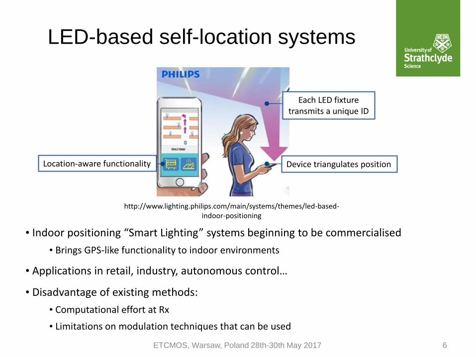
http://www.lighting.philips.com/main/systems/themes/led-based-indoor-positioning
Device triangulates position
Each LED fixture transmits a unique ID
Location-aware functionality
ETCMOS, Warsaw, Poland 28th-30th May 2017 6
LED-based self-location systems
• Indoor positioning “Smart Lighting” systems beginning to be commercialised
• Brings GPS-like functionality to indoor environments
• Applications in retail, industry, autonomous control…
• Disadvantage of existing methods:
• Computational effort at Rx
• Limitations on modulation techniques that can be used
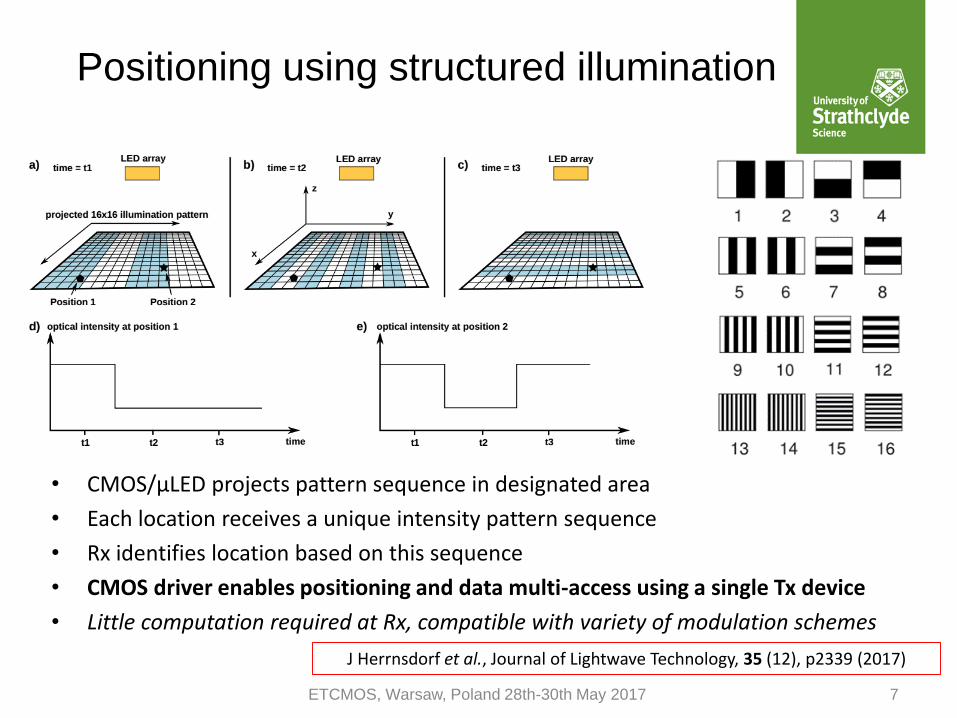
• CMOS/µLED projects pattern sequence in designated area
• Each location receives a unique intensity pattern sequence
• Rx identifies location based on this sequence
• CMOS driver enables positioning and data multi-access using a single Tx device
• Little computation required at Rx, compatible with variety of modulation schemes
ETCMOS, Warsaw, Poland 28th-30th May 2017 7
Positioning using structured illumination
J Herrnsdorf et al., Journal of Lightwave Technology, 35 (12), p2339 (2017)
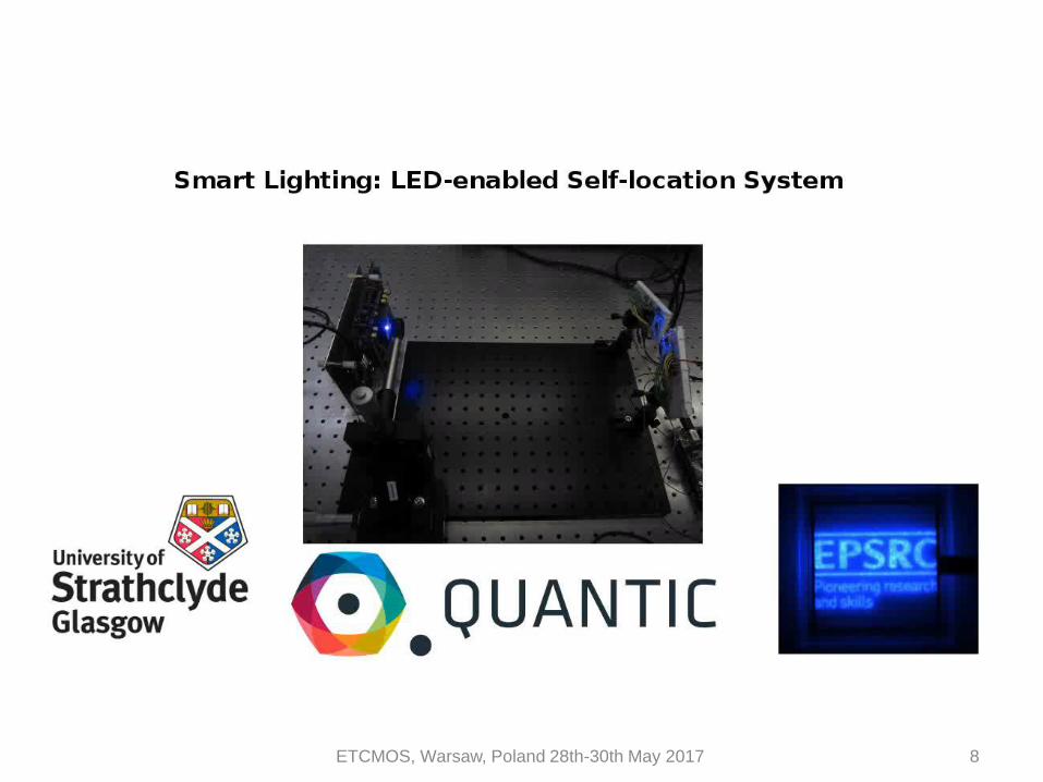
ETCMOS, Warsaw, Poland 28th-30th May 2017 8
ETCMOS, Warsaw, Poland 28th-30th May 2017 9
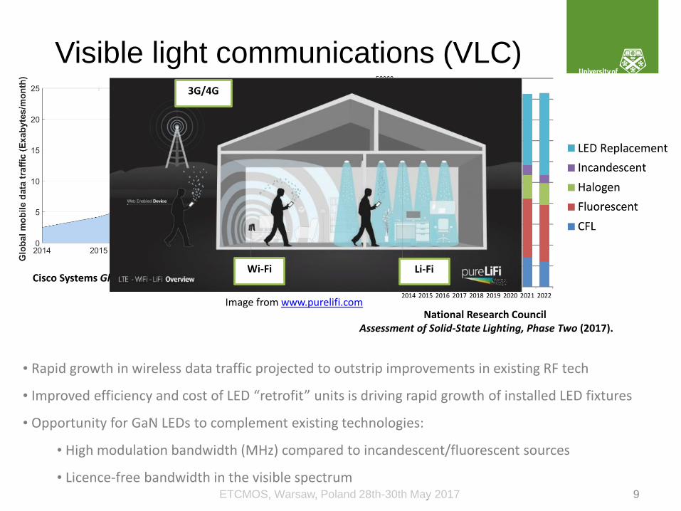
Visible light communications (VLC)
Cisco Systems Global Mobile Data Traffic Forecast 2014-2019
• Rapid growth in wireless data traffic projected to outstrip improvements in existing RF tech
• Improved efficiency and cost of LED “retrofit” units is driving rapid growth of installed LED fixtures
• Opportunity for GaN LEDs to complement existing technologies:
• High modulation bandwidth (MHz) compared to incandescent/fluorescent sources
• Licence-free bandwidth in the visible spectrum
National Research CouncilAssessment of Solid-State Lighting, Phase Two (2017).
Wi-Fi
3G/4G
Li-Fi
Image from www.purelifi.com
ETCMOS, Warsaw, Poland 28th-30th May 2017 10
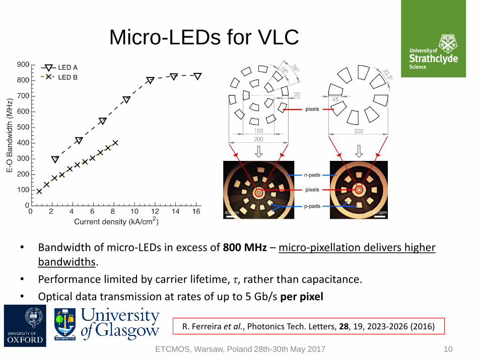
Micro-LEDs for VLC
• Bandwidth of micro-LEDs in excess of 800 MHz – micro-pixellation delivers higher bandwidths.
• Performance limited by carrier lifetime, τ, rather than capacitance.
• Optical data transmission at rates of up to 5 Gb/s per pixel
R. Ferreira et al., Photonics Tech. Letters, 28, 19, 2023-2026 (2016)
ETCMOS, Warsaw, Poland 28th-30th May 2017 11
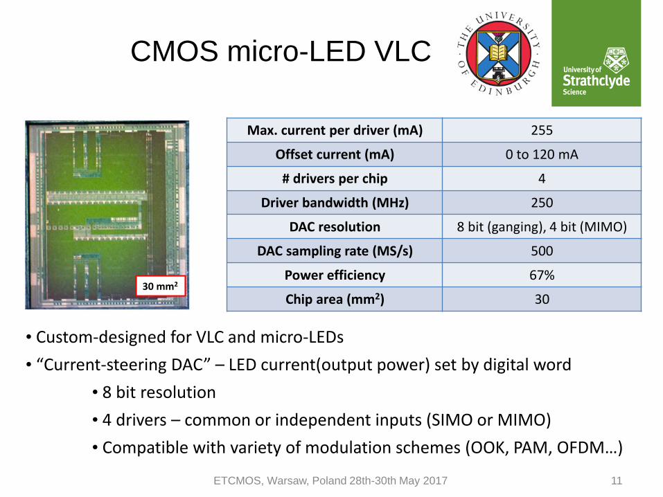
CMOS micro-LED VLC
30 mm2
Max. current per driver (mA) 255
Offset current (mA) 0 to 120 mA
# drivers per chip 4
Driver bandwidth (MHz) 250
DAC resolution 8 bit (ganging), 4 bit (MIMO)
DAC sampling rate (MS/s) 500
Power efficiency 67%
Chip area (mm2) 30
• Custom-designed for VLC and micro-LEDs
• “Current-steering DAC” – LED current(output power) set by digital word
• 8 bit resolution
• 4 drivers – common or independent inputs (SIMO or MIMO)
• Compatible with variety of modulation schemes (OOK, PAM, OFDM…)
ETCMOS, Warsaw, Poland 28th-30th May 2017 12
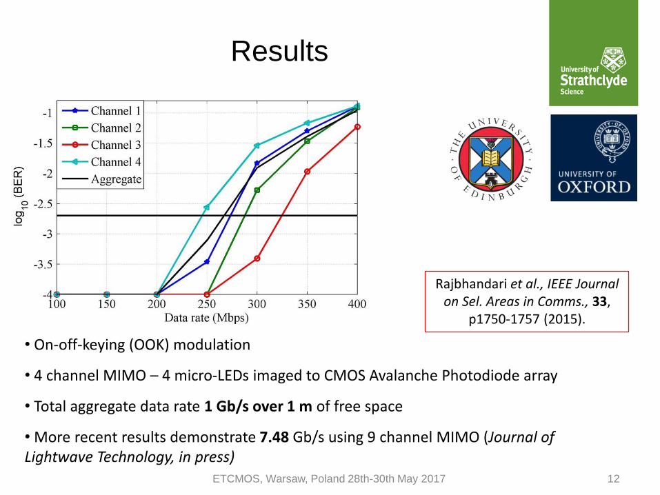
Results
• On-off-keying (OOK) modulation
• 4 channel MIMO – 4 micro-LEDs imaged to CMOS Avalanche Photodiode array
• Total aggregate data rate 1 Gb/s over 1 m of free space
• More recent results demonstrate 7.48 Gb/s using 9 channel MIMO (Journal of Lightwave Technology, in press)
Rajbhandari et al., IEEE Journal on Sel. Areas in Comms., 33,
p1750-1757 (2015).
ETCMOS, Warsaw, Poland 28th-30th May 2017 13
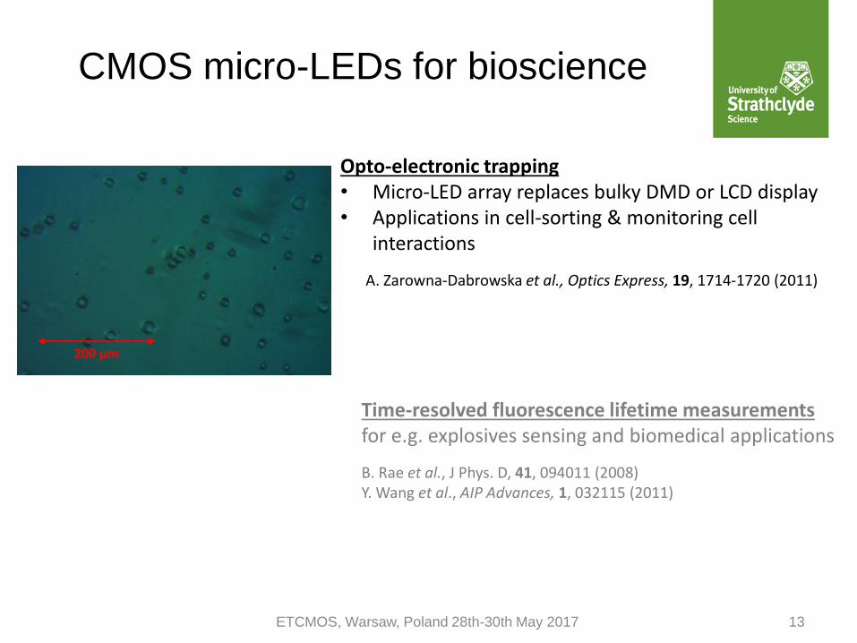
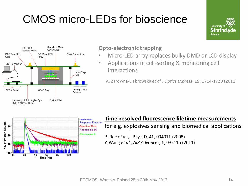
CMOS micro-LEDs for bioscience
Opto-electronic trapping• Micro-LED array replaces bulky DMD or LCD display• Applications in cell-sorting & monitoring cell
interactions
A. Zarowna-Dabrowska et al., Optics Express, 19, 1714-1720 (2011)
200 µm
Time-resolved fluorescence lifetime measurementsfor e.g. explosives sensing and biomedical applications
B. Rae et al., J Phys. D, 41, 094011 (2008)Y. Wang et al., AIP Advances, 1, 032115 (2011)
ETCMOS, Warsaw, Poland 28th-30th May 2017 14
CMOS micro-LEDs for bioscience
Opto-electronic trapping• Micro-LED array replaces bulky DMD or LCD display• Applications in cell-sorting & monitoring cell
interactions
A. Zarowna-Dabrowska et al., Optics Express, 19, 1714-1720 (2011)
200 µm
Time-resolved fluorescence lifetime measurementsfor e.g. explosives sensing and biomedical applications
B. Rae et al., J Phys. D, 41, 094011 (2008)Y. Wang et al., AIP Advances, 1, 032115 (2011)
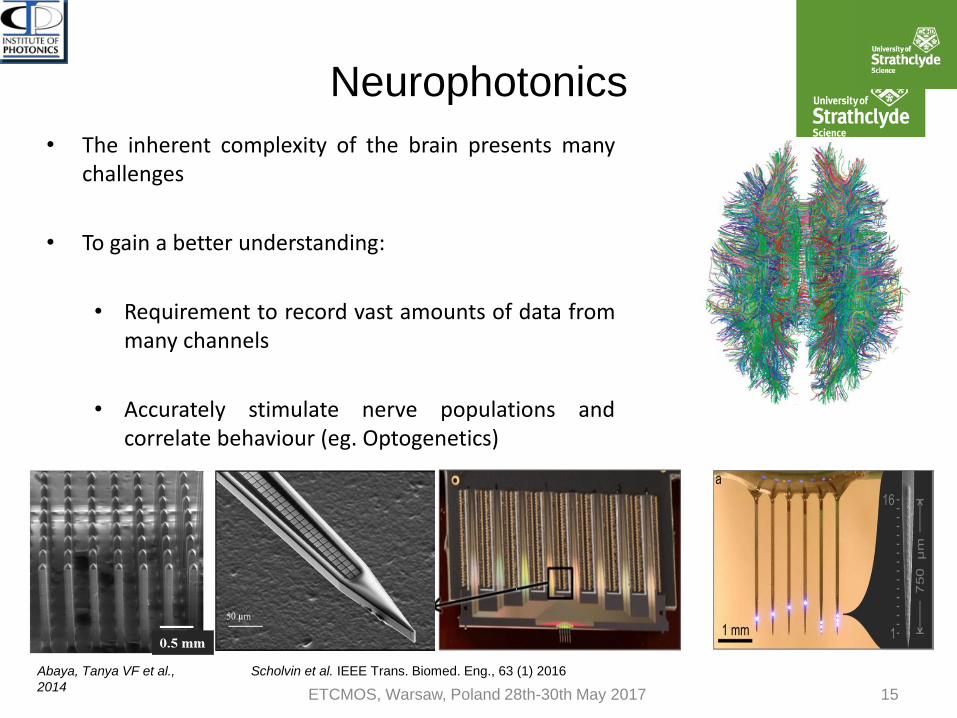
Neurophotonics
• The inherent complexity of the brain presents manychallenges
• To gain a better understanding:
• Requirement to record vast amounts of data frommany channels
• Accurately stimulate nerve populations andcorrelate behaviour (eg. Optogenetics)
Scholvin et al. IEEE Trans. Biomed. Eng., 63 (1) 2016Abaya, Tanya VF et al.,
2014ETCMOS, Warsaw, Poland 28th-30th May 2017 15
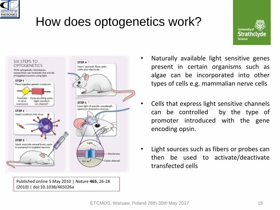
How does optogenetics work?
• Naturally available light sensitive genespresent in certain organisms such asalgae can be incorporated into othertypes of cells e.g. mammalian nerve cells
• Cells that express light sensitive channelscan be controlled by the type ofpromoter introduced with the geneencoding opsin.
• Light sources such as fibers or probes canthen be used to activate/deactivatetransfected cells
Published online 5 May 2010 | Nature 465, 26-28 (2010) | doi:10.1038/465026a
ETCMOS, Warsaw, Poland 28th-30th May 2017 16
ETCMOS, Warsaw, Poland 28th-30th May 2017 17
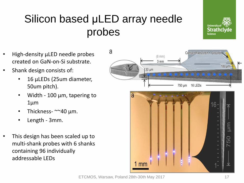
Silicon based μLED array needle
probes
• High-density μLED needle probes created on GaN-on-Si substrate.
• Shank design consists of:
• 16 μLEDs (25um diameter, 50um pitch).
• Width - 100 μm, tapering to 1μm
• Thickness- ~~40 μm.
• Length - 3mm.
• This design has been scaled up to multi-shank probes with 6 shanks containing 96 individually addressable LEDs
ETCMOS, Warsaw, Poland 28th-30th May 2017 18
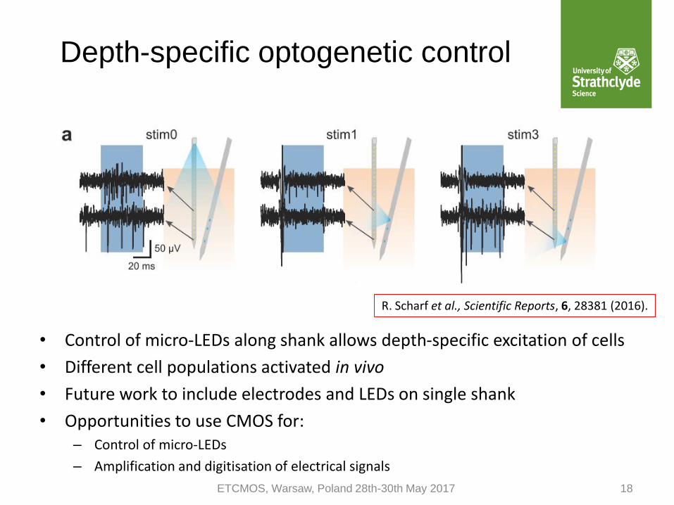
Depth-specific optogenetic control
R. Scharf et al., Scientific Reports, 6, 28381 (2016).
• Control of micro-LEDs along shank allows depth-specific excitation of cells
• Different cell populations activated in vivo
• Future work to include electrodes and LEDs on single shank
• Opportunities to use CMOS for:– Control of micro-LEDs
– Amplification and digitisation of electrical signals
ETCMOS, Warsaw, Poland 28th-30th May 2017 19
Summary
• GaN micro-LEDs:
– High brightness micro-scale displays
– Fast (Hundreds of MHz) modulation
– (Sub)-nanosecond optical pulses
– Can be integrated with CMOS electronics
• Demonstrated applications include:
– “Smart lighting”
– Visible light communications
– Bioscience, neurophotonics
– High-brightness micro-displays
Institute of Photonics
• Prof. Martin Dawson
• Dr. Keith Mathieson
• Dr. Erdan Gu
• Dr. Ian Watson
• Dr. Michael Strain
• Dr. Johannes Herrnsdorf
• Dr. Enyuan Xie
• Dr. Niall McAlinden
• Dr. Benoit Guilhabert
• Mr Alex Griffiths
• Mr Gabor Varkonyi
• Mr Ricardo Ferreira
ETCMOS, Warsaw, Poland 28th-30th May 2017 20
Acknowledgements
University of Edinburgh
• Prof. Harald Haas
• Prof. Robert Henderson
• Dr. Stefan Videv
• Mr Mohamed Islim
University of Oxford
• Prof. Dominic O’Brien
• Mr Graham Faulkner
• Dr. Hyunchae Chun
• Dr. Ariel Gomez-Diaz
University of Glasgow
• Dr. Tony Kelly
• Dr. Scott Watson
• Mr Shaun Viola
University of Coventry
• Dr. Sujan Rajbhandari

Thank you for your attention
www.strath.ac.ukwww.strath.ac.uk/science/physics/instituteofphotonics