Embed Size (px)
Citation preview

Student Manual
for
The Art of Electronics
Thomas C Hayes Paul Horowitz
Harvard University
rmiddot-~--~---~--~ -~---~-
Tlrl right oflht UfliverSil) (ljCumOridgr
loprilll arnildl all maMer oj bookl
WUJ grontdf by Hellry pm ill 1534
Tlu UliversJ Iros pllflld and published Crlfrtilluousty
sinN 1584
CAMBRIDGE UNIVERSITY PRESS
Cambridge
New York Port Chester Melbourne Sydney
82
CHAPTERS 2 3
Overview
A novel and powerful new sort of circuit performance appears in this chapter a circuit that can amplify Sometimes the circuit will amplify voltage thats what most people think of as an amplifiers job Sometimes the circuit will amplify only current in that event one can describe its amplification as a transformation of impedances As you know from your work in Chapter 1 that is a valuable trick
The transistors introduced in this chapter are called bipolar (because the charge carrying mechanism uses carrier of both polarities-but that is a story for another course) In the chapter that follows you will meet the other sort of transistor which is called field effect rather than unipolar (though they were called unipolar at first) The FET typeltwas developed later but has turned out to be more important than bipolar in digital devices You will see much of these FET logic circuits later in this course In analog circuits bipolar transistors still dominate but even there FETs are gaining
An understanding of transistor circuits is important in this course not so much because you are likely to design with discrete transistors as because you will benefit from an understanding of the innards of the integrated circuits that you are certain to rely on After toiling through this chapter you will find that you can recognize in the schematic of an otherwise-mysterious IC a collection of familiar transistor circuits This will be true of the operational amplifier that will become your standard analog building block Recognizing familiar circuits you will consequently recognize the op amps shortcomings as shortcomings of those familiar transistor circuit elements
Chapter 2 is difficult It requires that you get used to a new device and at the same time apply techniques you learned in Chapter 1 you will find yourself worrying about impedances once again arranging things so that circuit-fragment A can drive circuit shyfragment B without undue loading you will design and build lots of RC circuits often you will need a Thevenin model to help you determine an effective R We hope of course that you will find this chance to apply new skills gratifying but you are likely to find it taxing as well
Chapter 3 on FETs is difficult too and for similar reasons you must apply skills recently acquired as you design with a new class of devices Fortunately some of what you learn in Chapter 2 applies by analogy to the FETs of Chapter 3 gain as transconductance for example (gm current out per voltage in) is a notion equally useful in the two chapters Nevertheless both chapters will make your work hard and the varieties of FETs will annoy you for a while
We say this not to discourage you but on the contrary to let you know that if you have trouble digesting Chapter 2 thats not a sign that theres something wrong with you This is a rich chapter
In Chapter 4 suddenly your life as a circuit designer will become radically easier Operational amplifiers used with feedback will make the design of very good circuits very easy At that point you may wonder why you ever labored with those difficult discreteshytransistor problems But we wont reveal this to you now because we dont want to sap your present enthusiasm for transistors In return for your close attention to their demands transistors will perform some pretty impressive work for you
IN2-2
Instead approachil before ChI They coul voltage Sl
forward to microcircl
Figure IN2 (its not
83 IN2-2 Chs 2 3 Introduction
Instead of yearning for op amps lets try to put ourselves into a state of mind approaching that of the transistors three inventors who found to their delight two days before Christmas 1947 that they had constructed a tiny amplifier on a chunk of germanium They could envision a time when there would be no more vacuum tubes no more highshyvoltage supplies no more power wasted in heating filaments The world could look forward to the microcomputer the Walkman-and then the boom-box the amazingly tiny microcircuit housed in the amazingly huge suitcase Ah technology a circuit
pIe think middotvent one Om your
carrying J In the ~ld effect ype was ces You bipolar
because from an
m After tic of an ue of the ognizing hings as
ame time 19 about ~ circuitshy)ften you urse that taxing as
)ly skills what you ductance chapters
lill annoy
you have u This is
ly easier uits very discreteshy
tnt to sap demands
Figure IN231 The first transistor point-contact type (1947) Nobel prize-winning device looking wonderfully home-made (its not really made from paper clips scotch tape and chewing gum) Photo used with permission of ATampT Bell Labs
84 N4shy
Class 4 Transistors I First Model Text sec 20
Topics
bull Two simple views of transistor operation
Simple Ie = In bull ~
Simpler Ie = IE VEE = 06V
bull Applying the models standard circuits
Follower
Current source
common-emitter amp
push-pull
bull Recapitulation what the standard circuits look like
A TPreliminary Introductory Sketch
YoAn Intuitive Model in-) c
A transistor is a valve Text sec 20 Lab 4-2
smaU contl sjnat
(Is)
Figure N41 A transistor is a valve (not a pump)
Notice particularly that the transistor is not a pump it does not force current to flow it permits it to flow to a controllable degree when the remainder of the circuit tries to force current through the device
Ground Rules Text sec 201
Ground Rules For NPN type
1 V c gt VE (by at least a couple of tenths of a volt)
2 things are arranged so that VB - VE = about 06 v (VBE is a diode junction and must be forward biased)
We begin with two views of the transistor one simple the other very simple (Next time we will complicate things)
0 flow it ~s to force
a
Next time
N4-2 Class 4 Transistors I First Model 85
Text sec 201
Pretty simple current amplifier Ie = Beta bull In
~ l Ie =3Ia
Is ~ +1 Tc Is (1~)r8 Figure N42 Transistor as curren-controlled valve or amplifier
Very simple say nothing of Beta (though assume its at work)
bull Call V nE constant (at about 06 v)
bull call Ie = IE
A The simple view using Beta explicitly
You need the first view to understand how a follower changes impedances small (change in-) current in -gt large (change in-) current out
Text sec 203 Lab 4-2
SmaIL tI f
tVut = tvnr
lar3e bIE
v_
nut very different LIT s - ----shy
Figure N43 How a follower changes impedances
86 Class 4 Transistors I First Model N4-3
And here is a corny mnemonic device to describe this impedance-changing effect Imagine an ill-matched couple gazing at each other in a dimly-lit cocktail lounge-and gazing through a rose-colored lens that happens to be a follower Each sees what he or she wants to see
I
Figure N44 Follower as rose-colored lens it shows what one would ike to see
Complication Biasing ext sec 205
We can use a single power supply rather than two (both positive and negative) by pulling the transistors quiescent voltages off-center-biasing it away from zero volts
+15V
-Vmiddot+l5v
75k
Figure N45 Single-supply follower uses biasing
The biasing divider must be stiff enough to hold the transistor where we want it (with Vout around the midpoint between Vee and ground) It must not be too stiff the signal source must be able to wiggle the transistor s base without much interference from the biasing divider
The biasing problem is the familiar one Device A drives B B drives C As usual we want Zout for each element to be low relative to Zin for the next
(a 5hofj itt bloc~~1 sJnal ~lies) CAp3C~ amp8
Routrll amp8 hemiddot ln C
(bi 3~) (+ransisinr)
~iQ rv _1 j VaAS
Figure N46 Biasing arrangement
You will notice that the biasing divider reduce the circuits input impedance by a factor of ten That is regrettable if you want to peek ahead to complications see the bootstrap circuit (sec 217) for a way around this degradation
N4-4
You wi not only
Text sec 205
Forexa
bull t i
bull t c f
B The si
We car Beta Try
(
bull c
This is lets one S(
bull 1 Text Sec 203
N4-3
Imagine Id gazing she wants
gative) by olts
tnt it (with the signal ~ from the
usual we
a factor of bootstrap
N4-4 Class 4 Transistors I First Model 87
You will have to get used to a funny convention you will hear us talk about impedances not only at points in a circuit but also looking in a particular direction
Text sec 205
For example we will talk about the impedance at the base in two ways
bull the impedance looking into the base (this is a characteristic of the transistor and its emitter load)
bull the impedance at the base looking back toward the input (this characteristic is not detennined by the transistor it depends on the biasing network and (at signal frequencies) on the source impedance
the impedance lookn9 V-t
~1 (bi~) CblcJ
b~u~er Rz ( 115)
lrSOurre ~
into floe base (thi v+is a characferistlc of
the -transistor and ifs emiHer lo~d) -~
+-- the lPedance It th~ base ~kin5 back Rpound -Iowa nI -Ie Infut (H- ch~racl-isflc IS Jd ltitlPr-IIne4 igtJ The shy
1rdnss for I it derds M the biqSi~ rgtefwork anti at S19 I fT-eZ~oes On the source I~pd~nce)
Figure N47 Impedances looking in specified directions
B The simplest view forgetting Beta We can understand-and even design- many circuits without thinking explicitly about
Beta Try the simplest view
bull Call V BE constant (at about 06 v)
bull call Ie = IE
This is enough to let one predict the perfonnance of many important circuits This view lets one seeshy
bull That a follower follows Text Sec 203
v+
rv nJ
Vovi = V
(thues a v_ Ol v de difereoce)
Figure N48 Follower
88 Class 4 Transistors I First Model
bull That a current source provides a constant output current Text sec 206
bull Text sec 207
+56v (applied)
once VB is fiKed VE foo is ri)(ed aM determines If
Figure N49 Current source
That a common-emitter amplifier shows voltage gain as advertised
CD wjj Ie YIn AVa
V
wjj Ie oJIe (tT) =gt WJj Ie of Vou t (la Jeuro Rc =gt Ia~ 1Voub)
tVB jgfe of V-=gt wlJje of VE 9 W~j Ie oJ IE ~ Ie
(SMa 1( Rt ~ ldye 11)
Figure N410 Common-emitter amp
bull That a push-pull works and also shows distortion Text sec 214
just Samese folow~rs
~---- ----shybullbullbull be l nei Mer cr or qJown uducfs tnl-il its vsEI ~ ot v Sa fhes a d~ad secfion at crossoVfr
Figure N41l Push-pull
Recapitulation the important transistor circuits at a glance
N4-5
To get you started on the process of getting used to what bipolar transistor circuits look like and to the crucial differences that come from what terminal you treat as output here is a family portrait stripped of all detail
N4-6
Ir
Next transistOI We will very sim
89 N4-5 N4-6 Class 4 Transistors I First Model
fllted
outfixed out
out
Bflxed Inio-q In ~E
out fi)(ed
fixed fi)(eA
FoUOIAlER CURRENT SOJRCpound AI1PLIFIE( SWITCH
Figure N412 The most important bipoJar transistor circuits sketch
Next time we will begin to use the more complicated Ebers-Moll model for the transistor But the simplest model of the transistor presented today will remain important We will always try to use the simplest view that explains circuit performance and often the very simplest will suffice
ircuits look put here is
90 X4-2
1 Draw a
PerhapsCh 2 Worked Example Emitter Follower Gradually
Text sec 204
The text works a similar problem in detail sec 204 The example below differs in describing an AC follower That makes a difference as you will see but the problems are otherwise very similar
Problem AC-coupledfollower Design a single-supply voltage follower that will allow this source to
drive this load without attenuating the signal more than 10
Let Vee = 15 v let Ie quiescent be 05 rnA Put the 3dB point around 100 Hz
+6v 2 Choos To say middot I
Source---- _ r----shy
Quiescer ~ Uilt In effect present dtrv
1 I I
I __ ~ __ J
Figure X41 Emitter Follower (your design) to let given source drive given load
Solution Before we begin perhaps we should pause to recall why this circuit is useful It does not
amplify the signal voltage in fact we concede in the design specification that we expect 3 Centersome attenuation we want to limit that effect But the circuit does something useful before
you met transistors could you have let a 10k source drive a 47k load without having to Here settle for a good deal of attenuation How much be sure tlt
Vee is biThe Text sets out a step-by-step design procedure for a follower as we have noted already (sec 204) We will follow that procedure and will try to explain our choices as we Center go along in scrupulous-perhaps painful-detail RThevenin
91
differs in Iblems are
to
ld
t does not we expect ful before having to
ave noted ices as we
X4-2 Ch 2 Worked Example Emitter fullower
1 Draw a skeleton circuit Perhaps this is obvious but start by drawing the circuit diagram without part values
Gradually we will fill those in bull bull v+
Sour(~ R-----c loOid
i[--1--- rv
-- middot -
------) __ -=_J Figure X42 Emitter follower skeleton circuit load is AC coupled
2 Choose RE to center Vout
To say this a little more carefully we should say
center Yout-quiescent given IC-quiescent
Quiescent means what it sounds like it means conditions prevailing with no input signal In effect therefore quiescent conditions mean DC conditions in an AC amplifier like the present design
+15v
t TQ =oA
am for mdfltint Vf 75V
-=) fC = ~ = 15kE o5A
Figure X43 Choose RE to center Vou
3 Center Vbase
Here well be a little lazier than the Text suggests by centering the base voltage we will be sure to miss centering Yout But well miss by only 06 v and that error wont matter if Ycc is big enough the error is about 4 if we use a I5-volt supply for example
Centering the base voltage makes the divider resistors equal that in turn makes their RThevenin very easy to calculate
92 Ch 2 Worked Example Emitter fullower X4-3
4 Choose bias divider Rs so as to make bias stiff enough
Stiff enough means by our rule of thumb ~ 110 Rm-at-base(DC) If we follow that rule we will hit the bias voltage we aimed for (to about 10)
I +15v
( rl5v 300k
I Rn~lok I=
cvrshy300k -shy -shy
Figure X44 Set Rm bias Rmbuo Rin-at-base is just ~ X R E as usual Thats straightforward What is not so obvious is that
we should ignore the AC-coupled load That load is invisible to the bias divider because the divider sets up DC conditions (steady state quiescent conditions) whereas only AC signals pass through the blocking capacitor to the load
That finishes the setting of DC conditions Now we can finish by choosing the coupling capacitor (also called blocking capacitor evidently both names fit this cap couples one thing blocks another)
5 Choose blocking capacitor
We choose C1 to form a high-pass filter that passes any frequency of interest Here we have been told to put f3dB around 100 Hz
The only difficulty appears when we try to decide what the relevant R is in our highshypass filter
c
R I = RJN poundr circu it-ll _ Rn (bias) 1 RN (af base)
Figure X45 What R fOT blocking cap as highmiddotpass
We need to look at the input impedance of the follower seen from this point The bias divider and transistor appear in parallel
Digression on Series versus Parallel
Stare at the circuit till you can convince yourself of that last proposition If you have trouble think of yourself as a little charge carrier-an electron if you like-and note each place where you have a choice of routes there the circuit offers parallel paths where the routes are obligatory they are in series Dont make the mistake of concluding that the bias divider and transistor are in series because they appear to come one after the other as you travel from left to right
So Zin followeT = RTH bias parallel (Rm at base) The slightly subtle point appears as you try to decide what (Rm at basJ ought to be Certainly it is ~ x something But x what Is it just R E which has been our usual answer We did use RE in choosing RTH for the bias divider
X4-4
But t current should 1
The 47k) a neglect
Thats ~ the two trick se equivall answer
Socl
Recap
Here what we
93 X4-3
that rule we
bvious is that ider because reas only AC
the coupling I couples one
~st Here we
in our highshy
1t The bias
tion -an e of are that
orne
as you try to It Is it just ias divider
X4-4 Ch 2 Worked Example Emitter fullower
But this time the answer is No its not just RE because the signal unlike the DC bias current passes through the blocking capacitor that links the follower with its load So we should put Rload in parallel with RE this time
The impedance that gets magnified by the factor p then is not 15k but (15k parallel 47k) about 15k4 or 375k Even when increased by the factor p this impedance cannot be neglected for a 10 answer
Rm 135k parallel 375k ~
Thats a little less than 34 of 135k (since 375k is a bit short of 3 x 135k so we can think of the two resistors as one of value R the other as 3 of those Rs in parallel (using the Texts trick see Ch 1 p6 shortcut no 2raquo Result we have 4 parallel resistors of 375k roughly equivalent to lOOk (By unnatural good luck we have landed within 1 of the exact answer this time)
So choose C1 for f3dB of 100Hz C1 = 1(21t 100Hzmiddot lOOk) 1(6middot 102 100 X 103 = (160) X 10-6 0016IlF
C1 = 002 IlF would be generous
Recapitulation
Here for people who hate to read through explanations in words is one picture restating what we have just done
+SII ~ ~~----~~ ~
~~=o5A
2 Choose RE -to CE-lIte r VE
4 Let ITh (bias) given IQ -shybe laquoRin (base)
RTh (base) ~ foMSk Place VB (g~ie5cet) ~100J anJun d midpoi nt (75v) ~ rouJhly cen~riJ Vout (Vt)
This Juines rdtio Rt R2
hue 1 = fz
Figure X46 Followa design recapitulation
94 L4-2
Lab 4 Transistors I 4-2 Em
Wire up Drive 1Reading Chapter 201 - 208
offsetProblems Problems in text
that CorrAdditional Exercises 13 If youBad Circuits A B D E
do you 2N4400 characte4~1 Transistor Junctions are Diodes
Here is a method for spot-checking a suspected bad transistor the transistor must look like a pair of diodes when you test each junction separately But caution do not take this as a description of the transistors mechanism when it is operating it does not behave like two back-to-back diodes when operating (the following circuit made with a pair of diodes would be a flop indeed)
COLLECToR
Now TO-92 ground
CASE
B C f Figure L41 Transistor junctions (for testing not to describe transistor operation)
MeasuGet a 2N3904 NPN transistor identify its leads and verify that it looks like the object
shown in figure 22 of the text (and reproduced just above) by measuring the voltage across the BC and BE junctions using a DVMs diode test function (Most meters use a diode symbol to indicate this function) The diode test applies a small current (a few milliamps current flowing from Red to Black lead) and the meter reads the junction voltage You can even distinguish BC from BE junction this way the BC junction is the larger of the two the lower current density is revealed by a slightly lower voltage drop
In the las signal sot
a) Me output anI less than with omit
must look ot take this )ehave like of diodes
the object tage across lse a diode milliamps
e You can he two the
L4-2 Lab 4 Transistors I 95
4-2 Emitter Follower Wire up an NPN transistor as an emitter follower as shown below
Drive the follower with a sine wave that is symmetrical about zero volts (be sure the dc offset of the function generator is set to zero) and look with a scope at the poor replica that comes out Explain exactly why this happens
If you tum up the wavefonn amplitude you will begin to see bumps below ground How do you explain these (Hint see VBE breakdown specification in the data sheet for the 2N4400 transistor Text Appendix K the 4400 is very similar to the 3904 and in this characteristic is identical)
+5 voJfs (=vce)
270 In
2N3904
out 331ltshy
VEE --shy
Figure L42 Emitter follower The small base resistor is often necessary to prevent oscillation
Now try connecting the emitter return (the point marked VEE) to -15V instead of ground and look at the output Explain the improvement
(shy4-3 Input and Output Impedance of Follower
Measure 2in and 20ut for the follower below +5 volts
-sIhgtlh
17 t out -shy --I ~+- --l
I
) 1k cmiddot -~ -
Figure L43 Follower circuit for measuring lin and lout
In the last circuit replacethe small base resistor with a 10k resistor in order to simulate a signal source of moderately high impedance ie low current capability (see figure above)
a) Measure Zout the output impedance of the follower by connecting a lk load to the output and observing the drop in output signal amplitude for this use a small input signal less than a volt Use a blocking capacitor shy why (Hint in this case you could get away with omitting the blocking cap but often you could not)
96 Lab 4 Transistors I L4-3
Suggestions for measurement ofzut
bull If you view the emitter followers output as a signal source in series with Zout
Tbevcnln then the lk load fonns a divider at signal
frequencies where the impedance of the blocking capacitor is negligibly small
bull The attenuations are likely to be small To measure them we suggest you take advantage of the percent markings on the scope screen
Here is one way to do this measurement
center the wavefonn on the 0 mark
AC couple the signal to the scope to ensure centering
adjust amplitude to make the peak just hit 100
now load the circuit and read the amplitude in percent
b) Remove the lk load Now measure Zin which here is the impedance looking into the transistors base by looking alternately at both sides of the 10k input resistor For this measurement the 33k emitter resistor is also the load Again use a small signal Does the result make sense (See Text sec 203 subsection on impedances)
When you have measured Zin and Zout infer your transistors ~
~ Single-Supply Follower +15 volts
yF ---) +
Figure L44 Single supply follower A 270 ohm resistor in series with the base may be necessary if the circuit exhibits oscillations (This puzzling trick you will find explained in Lab 11 on oscillators)
The figure above shows a properly-biased emitter follower circuit operating from a single positive supply voltage This circuit comes from the example in Text sec 205 Wire it up and check it for the capability of generating large output swings before the onset of clipping For largest dynamic range amplifier circuits should exhibit symmetrical clipping
A fine point in fact the clipping here may look slightly odd a bit asymmetric To see why watch the base with one channel of the scope (not the same DC level as at the function generator nb) What happens when the voltage at the base tries to climb above the positive supply
L4-4
4-5 Tran You sa
at several currents
Try va 100k47~
06V) an
4-6 Cur
Construe sink)
Slowly What hal the curre~
Even the load making initial ex
in ~nal
r is
we ope
L4-3
ing into the )r For this gnal Does
uit exhibits
ing from a 205 Wire he onset of ymmetrical
ric To see [he function I above the
L4-4 Lab 4 Transistors I 97
4middot5 Transistor Current Gain You saw the transistors current gain p at work in 4-3 Now measure p (or hFE) directly
at several values of Ic with the circuit shown below The 47k and 1k resistors limit the currents Which currents do they limit and to what values
Try various values for R using a resistor substitution box eg 47 M 1 M 470K 100k47k Estimate the base current in each case (dont bother to measure it assume VUE = 06V) and from the measured Ic calculate p(hFE)
+15 vol-ls
1)lt
R -+5vol+S~
7
Figure U S Circuit for measurement of 13 or hFE
4middot6 Current Source
170
C -0+ ~ ~+15 (tOQ) 0-lOmA
+ 5 ---11---------1 2N3~04
820
-shy
Figure U6 Transistor current source
Construct the current source shown above (sometimes called more exactly a curren t sink) lit-
Slowly vary the 49laquo variable load and look for changes in current measured by the YOM What happens at maximum resistance Can you explain in tenns of voltage compliance of the current source
Even within the compliance range there are detectable variations in output current as the load is varied What causes these variations Can you verify your explanation by making appropriate measurements (Hint Two important assumptions were made in the initial explanation of the current source circuit in the Texts fig 221 sec 206)
98 Lab 4 Transistors I L4-5 L4-6
147 Commonmiddotemitter Amplifier 4middot9 Trar The c
on is salb 2N4400 i you have when on
Figure lA7 Common-emitter amplifier
Wire up the common emitter amplifier shown above What should its voltage gain be Check it out Is the signals phase inverted
Is the collector quiescent operating point right (that is its resting voltage) How about Turn th the amplifiers low frequency 3dB point What should the output impedance be Check it What is II by connecting a resistive load with blocking capacitor (The blocking cap again lets you test impedance at signal frequencies without messing up the biasing scheme) SaturatiOJ
shy
8 Emitter Follower Buffer (omit this exercise ifyou are short of time) Measl Hook an NPN emitter follower to the previous amplifier Think carefully about resistor coupling and bias Use a lk emitter resistor results pr
saturation
Figure lA8 Follower buffering amplifier (details left to you)
Measure output impedance again using a small signal Is the overall amplifier gain affected by the addition of the emitter follower
Why shoul VCE(sat) tha
L4-5
e gain be
Howabout Check it in lets you
ully about
Jlifier gain
L4-6 Lab 4 Transistors I 99
4middot9 Transistor Switch The circuit below differs from all the circuits you have built so far the transistor when
on is saturated In this regime you should not expect to see Ic = ~ bull In Why not The 2N4400 is a small power transistor housed in the T092 package like the 2N3904 which you have been using in this lab The 2N4400 can dissipate more power than the 3904 and when on shows lower V CE(sat) (see below)
1k
+5 volts
47 lamp (O15A) 3v)
Figure U9 Transistor switch
e C E
Turn the base current on and off by pulling one end of the resistor out of the breadboard What is In roughly What is the minimum required ~
Saturation or On voltage VCE(sal
Measure the saturation voltage V CE(sat) with DVM or scope Then parallel the base resistor with 150 ohms and note the improved V CE(sat) Compare your results with the results promised by the data set out below (See Appendix G in the text for more on saturation)
10
I =500 A 08
~ ~ 06
III
~M Ie =lA ~ =10A 4 =looA
D
o I 11 I t I
10) A l(0)A lA 10A
Base Gvrren( Ia Figure UIO 2N4400 Saturation voltage versus 10 and Ie
Why should the designer of a switching circuit be concerned with the small decrease in VCE(sat) that results from generous base drive
163
CHAPTERS 4 5 6
FEEDBACK Op amps oscillators power supplies
Overview
~ - L IJ 1h I shy
~ K+I lJ pound - Jt I t- -Iegtpound - If-Ie
f -Z+ -- +- L bull J
1lt =r
_ -Lk
~
Figure OVR41 Harold Blacks notes on the feed forward amplifier conceived as he rode the ferry from Staten Island to work one summer morning in 1927 (Copyright 1977lEEE Reprinted with pemrission from Harold S Black Inventing the
Negative Feedback Amplifier IEEE Spectrum Dec 1977)
We have been promising you the pleasures of feedback for some time You probably know about the concept even if you havent yet used it much in electronics Now at last here it is
Feedback is going to become more than just an item in your bag of tricks it will be a central concept th at you find yourself applying repeatedly and in a variety of contexts some far from operational amplifiers Already you have seen feedback in odd corners of transistor circuits you will see it constantly in the next three chapters then you will see it again in a digital setting when you build an analog-to-digital converter in Lab 17 and then a phase-locked-loop in the same lab It is a powerful idea
164 Chs 4 5 6 Feedback Op amps oscillators power supplies
Here is a Chapter four begins as Chapter two did with a simple idealized view of the new through whidevices-this time operational amplifiers little high-gain differential amplifiers that make perfonnanceit easy to build good feedback circuits As the chapter continues we soon feel obliged once
again to disillusion you- to tell you about the ways that op amps are imperfect At the same time we continue throughout these four labs to look at additional applications for feedback and we never lose our affection for these circuits They work magically well The third op amp lab Lab 10 introduces the novelty of positive feedback feedback of the sort that makes a circuit unstable Sometimes that is useful and sometimes it is a nuisance we look at cases of both sorts Several of the circuits that use positive feedback are oscillators a circuit type treated primarily in Chapter 5 (Active Filters and Oscillators)
Lab 11 concentrates on FETs this time used as switches but this lab includes circuits that use feedback and among them is the only active filter that you will meet in this course
Lab 12 returns us to circuits that for the most part rely on negative feedback but these are specialized circuits designed for the narrow but important purpose of providing stable power supplies The Text devotes a chapter to these circuits (Chapter 6 Voltage Regulators and Power Circuits) we give them a lab and hope that you will feel the continuity between this use of feedback and the more general cases that you met first in Chapter 4 With Lab 12 we conclude the analog half of the course and with the very next lab you will find the rules of the game radically changed as you begin to build digital circuits But we will save that story til later
A piece of advice (unsolicited) How to get the greatest satisfaction out of the feedback circuits you are about to meet
Here are two thoughts that may help you to enjoy these circuits
bull as you work with an op amp circuit recall the equivalent circuit made without feedback and the difficulties it presented for example the transistor follower both bipolar and FET or the transistor current sources The the op amp versions in general will work better to an extent that should astonish you
You have labored thr()ugh two difficult chapters 2 and 3 and have learned how to work around annoying characteristics of both sorts of transistor Now you are entitled to enjoy the ease of working with op amps and feedback
Figure OVR42 F
Pat yourself 0
A second tt
bull Recal obvic was a inven
The faded and remind you oj that the invenl newspaper wh facsimile of d appeared in ar invention Ne a newspaper I chance to write
------------ -
Chs 4 5 6 Feedback Op amps oscillators power supplies 165
Here is a picture of you climbing-as you are about to do---out of the dark valleys f the new through which you have toiled up into that sunny region above the clouds where circuit that make performance comes close to the ideal liged once
1 At the ~ ~ cgt ~
ations for ~~Ially well -----shydfack of the rlQo oa (1~ ~~KN nuisance
hea ven1i ~uddjback are -------_tors) ~
~ ~s circuits (1 )
s Course -----------------shy these are ---- o1z lt~
L-~~~ ---- _ _ ----- ng stable egulators I between gt~)d-k ~~- _ ~~~~~td~ ~~~LJ~-With Lab --1Ju-----e--- M poundif f r effect f- - Cu b C 00
I find the (~I 7f7771 _ - ~)-77 iF _ C-5 f7 will save ()i5fII SloliCjho ------ weiJr~ student
( If Moll~ V -) ( ~J~- )I( - rJ)
feedback te Vil[gt u atlA r e - J - ef(f( ts ~ 5 hIlt or
t ar lV II--
without Figure OVR42 Righteous and deserving student about to be rewarded for his travails with discrete transistors he climbs into the sunny alpine meadows where feedback blooms ver both
rsions in Pat yourself on the back and have fun
A second thought to work to enjoy bull Recall that negative feedback in electronics was not always used was not always
obvious- as the Text points out in its opening to Chapter 4 and as Harold Black was able to persuade the patent office (Black comes as close as anyone to being the inventor of electronic feedback)
The faded and scribbled-on newspaper that is shown at the start of these notes is meant to remind you of this second point- meant to help us feel some of the surprise and pleasure that the inventor must have felt as he jotted sketches and a few equations on his morning newspaper while riding the Staten Island Ferry to work one summer morning in 1927 A facsimile of this newspaper recording the second of Blacks basic inventions in the field appeared in an article Black wrote years later to describe the way he came to conceive his invention Next time you invent something of comparable value dont forget to jot notes on a newspaper preferably in a picturesque setting- and then keep the paper till you get a chance to write your memoirs
N8-2
The two feedback
Class 8 Op Amps I Idealized View make ser
Topics
bull old
earlier examples of feedback
bull new
negative feedback a notion of wonderful generality feedback without op amps examples you have seen feedback with op amps
bull the Golden Rules bull Applications Two amplifiers bull Preconditions when do the Golden Rules apply bull More Applications improved versions of earlier circuits The case
terms (nl bull current source bull summing circuit bull follower bull current-to-voltage converter
bull A generalization strange things can sit within the feedback loop
bull sometimes we want the op amp to hide the strange thing bull sometimes we want the op amp to generate (strangeshy
thingyl
Preliminary Negative Feedback as a general notion
This is the deepest most powerful notion in this course It is so useful that the phrase at least has passed into ordinary usage-and there it has been blurred Lets start with some examples of such general use-~)Oe genuine cartoon (in the sense that it was not cooked up to illustrate our point) and three cartoons that we did cook up Ask yourself whether you see feedback at work in the sense relevant to electronics and if you see feedback is the
sense posItIve or negatIve WAY OUT WEST
In conve nasty II
Feedbac WELL (ov~ 8EfA1 A Gener PRE-rr~ 6001gt HDH) I GIJEiS HMOWoRKIN riOT THf is nasty FMTOT (lUT1fH- I ~ VfTZ COMo AC~05T ~tlT to mean
Harolc this way
o
Figure N81 Feedback same sense as in electronics Copyright 1985 Mark Stivers rust published in Sunertown News
its
iback loop
range thing lte (strangeshy
he phrase at rt with some gtt cooked up whether you iback is the
N8-2 Class 8 Op Amps I Idealized View 167
The two cases below are meant to raise the question To which op amp terminal is the feedback being applied (If you have not yet looked at the Text that question will not yet make sense to you We assume you know what an op amp is at this point)
~
~ (J
- (
- gt
6 --1 ) J
o
J~ tMl
vU
7
Figure N82 Negative feedback poor usage which terminal is gelling the feedback
The case below comes closer to fitting the electronic sense of negative feedback In op amp terms (not Hollywoods) whos playing what role
Crane oper-at-oshy(has on lever-) Cd nt ee resufs of his Cldions
He needs cornlt-hon sljn~b
Stcor I fJcon t
bull f-oM obserVer who watches r15 db and te I(s ecntroler hD-fo CDr~ct em
~ Kor Holden
Marloh BrJndo
Figure N83 Negative feedback a case pretty mueh like op amp feedbaek
In conversation people usually talk as if positive feedback is nice negative feedback is nasty In electronics the truth is usually just the opposite
Feedback in electronics
Generally speaking negative feedback in electronics is wondetful stuff positive feedback is nasty Nevertheless the phrase means in electronics fundamentally what it should be used to mean in everyday speech
Harold Black the first to apply negative feedback to electronic circuits described his idea this way
ttertQwn News
168 Class 8 Op Amps I Idealized View N8-3
Text sec 426 p 233
by building an amplifier whose gain is made deliberately say 40 decibels higher than necessary (lOOOO-fold excess on energy basis) and then feeding the output back to the input in such a way as to throwaway the excess gain it has been found possible to effect extraordinary improvement in constancy of amplification and freedom from nonlinearityl
Open-loop vsfeedback circuits Nearly all our circuits so far have operated open-Ioop--with some exceptions noted
below You may have gotten used to designing amplifiers to run open-loop (we will cure you of that) you would not consider driving a car open loop (we hope) and you probably know that it is almost impossible even to speak intelligibly open-loop
Examples of Feedback without Op Amps
We know that feedback is not new to you not only because you may have a pretty good idea of the notion from ordinary usage but also because you have seen feedback at work in parts of some transistor circuits
Lab 5 5-25-35-5
out otJt
f _( -
open-loop stabil ized
Figure N84 Some examples of feedback in circuits we have built without ~p amps j
Feedback with Op Amps Op amp circuits make the feedback evident and use a lot of it so that they perform better
than our improvised feedback fragments Op amps have enormous gain (that is their openshyloop gain is enormous the chip itself used without feedback would show huge gain 200000 at DC for the LF411 the chip you will use in most of our labs) As Black suggests op amp circuits throwaway most of that gain in order to improve circuit performance
1 IEEE Spectrum Dec 1977
NS-4
The Golden
Just as WI
remained su with a a sim even when but good ont
Text sec 403 p 177
Op
These simp It
Application
Two Ampliji Text sec 404 405 p 178
What are the
bull Wha bull App
settll
bull The grou calle implt
N8-3 N8-4 Class 8 Op Amps I Idealized View 169
Is 19 11
y
Ins noted will cure probably
etty good t work in
)rm better heir openshyuge gain As Black ve circuit
The Golden Rules
Just as we began Chapter 2 with a simple model of transistor behavior and that model remained sufficient to let us analyze and design many circuits so in this chapter we start with a a simple idealized view of the op amp and usually we will continue to use this view even when we meet a more refined model The golden rules (below) are approximations but good ones
Text sec 403p177
Op amp Golden Rules
1 The output attempts to do whatever is necessary to make the voltage difference between the two inputs zero
2 The inputs draw no current
These simple rules will let you analyze a heap of clever circuits
Applications
Two Amplifiers Text sec 404 405 p17S
Rz
In
~out In
_______ out
-
Jain = Rz 11 9aLn =
-
Figure NS5 Inverting and nonmiddot inverting amplifiers
What are the special virtues of each
bull What is Rin for inverting amp (Golden Rule 1 should settle that) bull Approximately what is Rin for the non-inverting amp (Golden Rule 2 should
settle that) bull The inverting amps inverting terminal (the one marked _) often is called virtual
ground Do you see why (Why ground Why virtual) This point often called by the suggestive name summing junction turns out to be useful in several important circuits
170 Class 8 Op Amps I Idealized View NS-5
When do the Golden Rules apply Text sec 408
Now that we have applied the Golden Rules a couple of times we are ready to understand that the Rules sometimes do not apply
bull note a preliminary assumption these rules are useful only for circuits that incJudeshy
1 Feedback and 2 Feedback of the right flavor negative feedback
bull And note the careful wording of the first rule the output attempts This rule is like a guarantee written by a cautious (and prudent) lawyer It warns a careful reader that the person designing op amp circuits retains an obligation to use his head apparently there are circuits in which the op amp will be unable to deliver the desired result it will attempt and fail Lets look at some such cases to be warned early on
Try your understanding of the golden rules and their restrictions by asking yourself whether the golden rules apply to the following circuits
p 182 item 2
works works works is fhere rdlad
Figure 186 Do the Golden Rules apply lO lhese circuilS
And will the outputs attempt to hold the voltages at its two inputs equal succeed in these cases
p 182 item ]
+lv --1--0
Figure N87 Willlhe OUlpUls allempl succeed here
More Applications Improved Versions of Earlier Circuits
Nearly all the op amp circuits that you meet will do what some earlier (open-loop) circuit did-but they will do it better This is true of all the op amp circuits you will see today in the lab Lets consider a few of these current source summing circuit follower and current-to-voltage converter
NS-6
Current So
(d a
The right-he thats broug hide both th that the FE~ source penlt naked FET time to get l
SummingC Text sec 409 p 185 fig 419 Lab 8-7
In the lab y offset of the
171 N8-5 N8-6 Class 8 Op Amps I Idealized View
Current Source
) understand
Iircuits that Vfn
V (dc or a poundi3 At) 1
This rule is I ~ I v~ns a careful -R Rn to use his 7o deliver the -shy
obewarned Figurc N88 Op amp current sources
The right-hand circuit gives you a chance to marvel at the op amps ability to make a device thats brought within the feedback loop behave as if it were perfect Here the op amp will
ing yourself
J hide both the slope of the In vs Vns curve in the saturation region (a slope that reveals that the FET is not a perfect current source) and the more radical departure from currentshysource performance in the linear region-a region one must stay out of when using a naked FET Are you beginning to see how the op amp can do this magic It takes some time to get used to these wonders At first it seems too good to be true
Summing Circuit Texi sec 409 p 185 fig 419
lc Lab 8-7 lk 11lt
lk
I succeed in
out ovt
100
7
passIve ccfive
Figurc N89 Summing Circuits
In the lab you will build a variation on this circuit a potentiometer lets you vary the DC offset of the op amp output
21(
7
l-loop) circuit j see today in follower and
Class S Op Amps I Idealized View NS-7172
Followers Text sec 406 sec 409p 186
Ollt
oen- loot version ac+ive version (no ed but bias not shown)
Figure N810 Op amp followers
How are the op amp versions better than the bare-transistor version The obvious difference is that all the op amp circuits hide the annoying O6V diode drop A subtler difference-not obvious by any means is the much better output impedance of the op amp circuits How about input impedance
Current-to-voltage con verter Text sec 409 p184
P)ofomefer IdeJL Current l1eter_--c=_-_ ~---=~~~~~~~~-----
(a fed problem)
R R
l R (me+emovement)
passive version
Figure N811 Two applications for I-to-V converter photometer ideal current meter
(A Puzzle if you and I can design an ideal current meter so easily why do our lab multimeters not work that way Are we that much smarter than everyone else)
NS-S
StrangeT The pus
amp can ta or diodes
Heres tI
In the pus I op amp 0
circuits h may be prl
Compare Text sec p 212fig 435
Figu
In both 0
proud of output (th
In toda loop with
Lab 8-6
Youll nifty CirCI
N8-7
r
obvious ~ subtler op amp
) our lab
N8-8 Class 8 Op Amps I Idealized View 173
Strange Things Can be put Into Feedback Loop The push-pull follower within the feedback loop begins to illustrate how neatly the op
amp can take care of and hide the eccentricities of circuit elements- like bipolar followers or diodes
Heres the cheerful scheme
1 Ul (tidj)
Sometirs gti5 is the ovi-pvt w tke the stra ojeness (doj-1 The f~Lgtre)
fI - OILt (tJ~)
_~ th ~ oufpvt W~ r~ +I3 To hide -tIoe J~
liigurc N8U Op Amps can tidy up after strange stuff within the loop
In the push-pull follower we treat the tidied-up signal as the output the strange tricks the op amp output needs to perform to produce a tidy output do not interest us In other circuits however the strange signal evoked by the strange stuff in the feedback loop may be precisely what does interest us Here are two examples
Compare Text sec 414 p 212fig 435
vigt -IAI~
Vin
out out
Figure N813 Two cases where we plant strange stuff in loop to get strange and interesting op amp output
In both of these cases far from trying to hide the dog (of Fig N812 above) we are proud of him so proud that we want to gaze at his image which appears at the op amp output (the image is always dog-I inverse-dog)
In todays lab you will be so bold as to put the oscilloscope itself inside one feedback loop with entertaining results
Lab 8-6
rhofo+nnss for Scofe amplifier
volta~e to inkns9f OSI tOn to vol+aje(~ In+enSI~)
Figurc N814 Scope brought within feedback loop adjusts location of CRT beam
Youl1 see lots of nifty circuits in this chapter Soon you may find yourself inventing nifty circuits Op amps give you wonderful powers (In case you find yourself wanting still
174
c
Class 8 Op Amps I Idealized View N8-9
more when you have concluded the orgy of cleverness that appears in the Circuit Ideas at the end of the Texts Chapter 4 see the books of application notes published by National Semiconductor among others or the application notes that follow many op amp data sheets including the LF411 s (see Text appendix K for the 411 s data sheet)
Two work
1 ill
2 a
1 bull (-100
The inv
F
Will any I impedanc(
A plaw impedanc golden ruJ
You dor how the 0
In this ca impedanc(
And he make it s~ be IOOOM admit that
N8-9
~uit Ideas at by National data sheets
Ch 4 Worked Examples Op Amps Idealized Two worked examples
1 an inverting amplifier
2 a summing circuit
1 bull (-100) Amp
Problem Inverting Amplifier
Design an inverting amplifier with a gain of -100 to be driven by a source whose output impedance is high and uncertain lOOk to 1MQ
The inverting amp is easy enough apart from the impedance issues
lOOR
R
~
Figure XSl Inverting amplifier-but postponing the questions that call for some thought part values
175
Will any pair of resistor values do in the ratio 100 1 Does the high and uncertain source impedance matter here
A plausible-but wrong-first response might be I dont have to worry about source impedance because op amps have giant input impedances that follows from the second golden rule which says the inputs draw no current
You dont fall for that answer though because you can see that the golden rule desclibes how the op amp behaves whereas what concerns us here is how the op amp circuit behaves In this case its input impedance is not the same as that of the op amp the circuit input impedance is much lower It isjustR J
1M Po
Rn=lOk 10k
-shy
Figure XS2 Rin of inverting amp as low as R1
And heres a plausible-but wrong- solution just make Rl much bigger than Rsource make it say 10Mn Thats a good thought but it implies that the feedback resistor should be 1000M-1 cn and that is excessive for reasons we will make sense of only when we admit that op amps are not quite as good as their idealized model
176 Ch 4 Worked Examples Op Amps Idealized X8-2
Easy solution to the impedance problem a follower
A follower solves the problem neatly
1M
Figure X83 f-ollower buffers (he input of the inverting amp
Now we can choose modest resistor values for the inverting amp like those shown above At first you may feel uncomfortable tacking in extra op amps to solve circuit problems We hope you will soon get over this discomfort A slogan worth remembering will recur in this chapter op amps are cheap They come 2 and even 4 to a package One more op amp is no big deal and often is the best way to refine a circuit
2 A ritllmetic
Problem S umming Circuit
Design a circuit that forms the following sum of the input voltages A B andC
= A + 2B -3CVout Again lets make the source impedances high and uncertain lOOk to IMn just to drum home our earlier point
And heres a solution It is so similar to the preceding problem that it does not call for much explanation Lets do the problem with just comments in balloons
A
c
Figure XS4 Summing circuit II
The function of this circuit-VoUI = A + 2B -3C-recalls why op amps were given that name they can do mathematical operations-and other fancier ones such as multiplication and division as well with the help of log amps
( 8-1 Open-I Before WI
firs pac
sec( men mea ordiJ mak the ( calle
Astound y( apply 0 volts (typical) = 20
X8-2
wn above lems We cur in this amp is no
0
)t call for
L 2B-C
siven that tiplication
Lab 8 Op Amps I
Reading Chapter 4 401-409 pp 175-187
Problems Problems in text Bad Circuits BDFGIKLM (none of these requires any deep understanding of op amps)
177
l ( 8-~ Open-Loop Test Circuit
Before we ask you to build your first op amp circuit we should remind you of two points
first how the integrated circuit (IC) package goes into the breadboard (The package style is called DIP dual in-line package)
00000 DO
o PDP 0 0 0 o 0 0 0 0 G G a Ie gtlost
Jl Jl Jl 0 0 snJ-dle i -1 fndboar-d
~ o [J
0000000
00000000
00000000
Figure LSl How the Ie op amp goes inlo lle breadboard il straddles the trench
second a point that may seem to go without saying but sometimes needs a mention the op amp always needs power applied at two pins nearly always that means plusmn15V in this course We remind you of this because circuit diagrams ordinarily omit the power connections On the other hand many op amp circuits make no direct connection between the chip and ground Dont let that rattle you the circuit always includes a ground-in the important sense common reference called zero volts
+ISshy
10kgt VI out
l
-ISshy1 2shy
3 t
-pm nvr7Ikrin (rY1Inl-tlIP cose)
Figure L82 Open-loop lest circuit
Astound yourself by watching the output voltage as you slowly twiddle the pot trying to apply 0 volts Is the behavior consistent with the 411 specification that claims Gain (typical) = 200VmV
i
178 Lab 8 Op Amps I L8 -2
(S-2 Inverting Amplifier 10k
lk
gt--+--- out
Figure LS3 Inverting amplifier
Construct the inverting amplifier drawn above Drive the amplifier with a 1kHz sine wave What is the gain What is the maximum output swing How about linearity (try a triangle wave) Try sine waves of different frequencies Note that at some fairly high frequency the amplifier ceases to work well sine in does not produce sine out (We will postpone until next time measuring the slew rate that imposes this linllt we are still on our honeymoon with the op amp it is still ideal Yes sweetheart your slewing is flawless)
Now drive the circuit with a sine wave at 1kHz again Measure the input impedance of this amplifier circuit by adding lk in series with the input
Measure the output impedance (or try to measure it anyway) Note that no blocking capacitor is needed (why) You should expect to fail here you probably can do no more than confirm that Zout is very low Do not nllstake the effect of the op amps limited current output for high Zout You will have to keep the signal quite small here to avoid running into this current linllt The following curves say this graphically
Vw-t(lIat) - volts
Source 5
-30 middot20 -10 10 20 30
-5 output cvrrent -A
Figure LS4 Effects of limit On op amp output current (LF41 1)
These curves say in compact form that the current is limited to plusmn2S rnA over an output voltage range of plusmn10V and youll get less current if you push the output to swing close to either rail (rail is jargon for the supply voltages)
L8-3
Note tl
a very sn load If a voltag~
Figure LSs
Dont 1001
poor stude
~) Non
Wire up the same a~
Try to n series with
On Rin ob~
scc
Does thi inverting ar redraw the ( as the inve]
L8 -2
a 1kHz sine nearity (try a Ie fairly high ut (We will re still on our hwless)
impedance of
bull no blocking n do no more mited current 1 running into
ver an output wing close to
179L8-3 Lab 8 Op Amps I
Note to zealots a student who tries very hard to measure Roul by loading the op amp with a very small resistor-say H2-may see a bizarre result the output amplitude grows under load If you see that you are seeing the effect of sneaky positive feedback applied through a voltage divider formed by the H110ad and the small resistance of the ground line
10k ImdJne ltl +lV lNin Convince jOu5~lf tAdt +he
1k
( cm2f~~dl~Lt~vt _ltJill HI ~pected -lOmVInut Signa L
] -test loadis 2llied acflt$S +Aese ----- shytogto foink ~3round1 ao2n Ine
lea r ofgt- P ~ Tfsshnre of 91Ound --~ vinny Inside breadfgt03d
frue JfVrmd [BNe sAell [power 5p0 relur-n (me
Figure LSS Sneaky positive feeltlback can boost the signal when small R10wlets substantial currents flow in the ground lines
Dont look for this exotic effect its not worth your time This note is addressed only to the poor student confronted with this strange behavior
~) Non-inverting Amplifier in 1 shy
out V i
lt o-j If)
- Llk
Figure LS6 Non-inverting amplifier
Wire up the non-inverting amplifier shown above What is the voltage gain (It is not the same as for the inverting amp you just built)
Try to measure the circuits input impedance at 1kHz by putting a 1Meg resistor in series with the input Here watch out for two difficulties
Once again beware the finding 10 M ohms
Rin is so huge that Cin dominates You can calculate what Cin must be from the observed value of f3dB bull Again make sure that your result is not corrupted by the scope probes impedance (this time its capacitance)
Does this configuration maintain the low output impedance you measured for the inverting amplifier (You can answer this question without doing the experiment if you r redraw the circuit to reveal that for the purpose of this measurement it is the same circuit as the inverting amp)
180 Lab 8 Op Amps I L8-4
8-4 Follower
~__shy out-
Figure LS7 Op amp follower
Build theolower shown above using a 411 Check out its perfonnance In particular measure (if possible) Zin and Zout (but dont wear yourself out you already know the answer if you recognize theolower as a special case of one of the circuits you built a few minutes ago)
8-5 Current Source -1-15
15k
lk
Figure LS8 Current source
Try the op-amp current source shown above What should the current be Vary the load pot and watch the current using a digital multimeter
Note that this current source although far more precise and stable than our simple transistor current source has the disadvantage of requiring a floating load (neither side connected to ground) in addition it has significant speed limitations leading to problems in a situation where either the output current or load impedance varies at microsecond speeds
The circuit below begins to solve the first of these two problems this circuit sources a current into a load connected to ground
27k
12k
70
lOA (DHM)
G C E
Figure LS9 Current source for load rerurned to ground
G D S
L8-5
Watch t when it d VCE or V[
Try us MOSFET 2N3906)
Should differenc( circuit pe either kin differenc( differenc(
~ Cur
a) PhotoiJ
Use an instead u similar) feedback
If you feedback circuit be) (Hint wh
What i~ will be re does the Look at t)
see
Make s converter
181 L8-4
)articular know the luilt a few
y the load
ur simple ~ither side roblems in d speeds
sources a
L8-5 Lab 8 Op Amps I
Watch the variation in lout as you vary Rload To understand why the current source fails when it does it may help to use a second meter to watch the voltage across the transistor VeE or VDS
Try using a bipolar transistor a 2N3906 Then replace that transistor with a VPOI MOSFET (its pinout is equivalent so you can plug it in exactly where you removed the 2N3906)
Should the circuit perfonn better with FET or with a bipolar transistor Do you find a difference that confirms your prediction Does the FETs linear region restrict the range of circuit perfonnance as it did for the simple FET current source you built in Lab 7 With either kind of transistor the current source is so good that you will have to strain to see a difference between FET and bipolar versions Note that you have no hope of seeing this difference if you try to use a VOM to measure the current use a DVM
e lcurrent to Voltage Converter -~--
fa) Photodiode I
lOMeg
c~-shy
LPT-l00 pound
(no colhfor LPT-IOO (oec tiol))
Figure L810 Photodiode photometer circuit
Use an LPT100 phototransistor as a photodiode in the circuit shown above (you may instead use an FPT100 or FPT110 pinouts are the same as for the LPT100 specs are very similar) Look at the output signal (if the dc level is more than 10 volts reduce the feedback resistor to 1Meg)
If you see fuzz on the output--oscillations-put a small capacitor in parallel with the feedback resistor 0001 IlF should be big enough for either this or the phototransistor circuit below even with its smaller Rfeedback Why does this capacitor douse the oscillation (Hint what does it do to the circuits gain at high frequencies)
What is the average dc output level and what is the percentage modulation (The latter will be relatively large if the laboratory has fluorescent lights) What input photocurrent does the output level correspond to Try covering the phototransistor with your hand Look at the summing junction (point X) with the scope as VOUI varies What should you middot see
Make sure you understand how this circuit is preferable to a simpler current-to-voltage converter a resistor used thus
LC3ft- n n 110M
LPT-l00
Figure L811 A less good pholodiode circuit
182 Lab 8 Op Amps I L8-6
b) Phototransistor +I~
(no bllse co fle C tion)
Figure LS12 Phototransistor photometer circuit
Now connect the LPTlOO as a phototransistor as shown just above (the base is to be left open as shown) What is the average input photocurrent now What about the percentage modulation Look again at the summing junction
c) Applying Ihe Pholometer Circuit (optional)
If you put the phototransistor at the end of a cable connected to your circuit you can let the transistor look at an image of itself (so to speak) on the scope screen (A BNC with grabbers on both ends is convenient note that in this circuit neither terminal is to be grounded so do not use one of the breadboards fixed BNC connectors) The image appears to be shy it doesnt like to be looked at by the transistor Notice that this scheme brings the scope within a feedback loop
Figure L813 Photosensor sees its own image
You can make entertaining use of this curious behavior if you cut out a shadow mask using heavy paper and arrange things so that the CRT beam just peeps over the edge of the mask In this way you can generate arbitrary waveforms
If you try this keep the amplitude of your cut-out waveform down to an inch or so Have fun this will be your last chance for a while to generate really silly waveforms say Diamond Head or Volkswagen or Matterhorn You will be able to do such a trick again- at least in principle--once you have a working computer which can store arbitrary patterns in memory in digital form Practical arbitrary-waveform generators use this digital method
L8-7
8-7 SUI
Thec aDCof
8-8 Pu
Build output 0
least a f should s
Listen should d
Now 1
figure 4 be elimil like T
Listen Why dk sine
Jfyou op amp t
L8-6
s to be left percentage
IOU can let BNC with II is to be fhe image lis scheme
jow mask dge of the
nch or so orms say ch a trick e arbitrary this digital
L8-7 Lab 8 Op Amps I 183
8-~I Summing Amplifier L--shy 10k
shy
59 ilt gt---+-- 5i9middotout
5Gv = -1 (offset ra~e = plusmn lOv
-15v~+15v 10k
OFFSET
Figure LS14 Summing circuit IX offset added to signal
The circuit in the figure above sums a DC level with the input signal Thus it lets you add a DC offset to a signal (Could you devise other op amp circuits to do the same task)
8-8 Push-pull Buffer
10k
~ look 2N390Li
390
-
-5
Figure LS15 Amplifier willi push-pull buffer
1k
-shy
Build the circuit shown above Drive it with a sine wave of 100Hz-500Hz Look at the output of the op-amp and then at the output of the push-pull stage (make sure you have at least a few volts of output and that the function generator is set for no dc offset) You should see classic crossover distortion
Listen to this waveform on the breadboard speaker But before you drive the speaker you should detennine the maximum safe amplitude given the following power ratings
transistors 350 mW speaker 250 mW
Now reconnect the right side of the feedback resistor to the push-pull output (as in Text figure 422) and once again look at the push-pull output The crossover distortion should be eliminated now If that is so what should the signal at the output of the op-amp look like Take a look (Doesnt the op amp seem to be clever)
Listen to this improved waveform does it sound smoother than the earlier waveform Why did the crossover distortion sound buzzy-like a higher frequency mixed with the sine
If you increase signal frequency you will discover the limitations of this remedy as of all op amp techniques you will find a glitch beginning to reappear at the circuit output
184 N9-2
1 Three
Class 9 Op Amps II Departures from Ideal bltegrato
To appl
Topics
bull old
passive versions of circuits now built with op amps integrator differen tiator rectifier
bull new
three more important circuits (applications)
bull integrator bull differentiator bull rectifier
op amp departures from ideal
bull offset voltage bull bias current
offset current bull frequency limitations open-loop gain slew rate bull output current limit
the simpl
PassiVt Text secii5 Lab 2-3
To make t Text sec ii5p
This kept we put a s But the ou
Opampvl Text sec 4i9 Lab 9-2
The op point to 0
Today we end our honeymoon with the op amp we admit it is not ideal But we continue to admire it we look at more applications and as we do we continue to rely on our first simplest view of op amp circuits the view summarized in the Golden Rules
After using the Golden Rules to make sense of these circuits we begin to qualify those rules recognizing for example that op amp inputs draw a little current Lets start with three important new applications then well move to the gloomier topic of op amp imperfections
ways
Theop saturation ofsymmet
200
Lab 9 Op Amps II
Reading Chapter 410-422 pp 187-229
Problems Problems in text Additional Exercises 1-4 Bad Circuits ACH
This lab introduces you to the sordid truth about op amps theyre not as good as we said they were last time Sorry But after making you confront op amp imperfections in the first exercise (9-1) we return to the cheerier task of looking at more op amp applications-where once again we treat the devices as ideal On the principle that a person should eat his spinach before the mashed potatoes (or is it the other way round) lets start by looking at the way that op amps depart from the ideal model
9-1 Op-amp Limitations
a Slew Rate
Figure L91 Slew rate measuring circuit (The series resistor prevents damage if the input is driven beyond the supply voltages)
Begin by measuring slew rate and its effects with the circuit above We ask you to do this in two stages
1) Square wave input Drive the input with a square wave in the neighborhood of 1kHz and look at the output
with a scope Measure the slew rate by observing the slope of the transitions
Suggestions
Find a straight central section avoid the regions near saturation-near the limits of output swing
Full slew rate is achieved only for strong overdrive a large difference signal seen at the input of the amplifier
The rates for slewing up and down may differ
See what happens as the input amplitude is varied
2) Sine input
Switch to a sine wave and measure the frequency at which the output amplitude begins to drop for an input level of a few volts Is this result with the slew rate that you measured in part 1) just above
L9-2
Now effect a] O5Vlls
hOjjsel
Now I
voltage
Note for this attributal choosin~ unusual
l)Mei
The tr so that y you nee negligibl
Comp
2) Mill
Trim t1
c Bias Now n
(either a ~ a lOKw your mea
I we said 1 the first Dp amp Ie that a round)
ou to do
le output
r
~
de begins measured
L9-2 Lab 9 Op Amps II 201
Now go back and make the same pair of measurements (slew rate and sine at which its effect appears) with an older op amp a 741 The 741 claims a typical slew rate of 05Vlls the 411 claims 15Vlls How do these values compare with your measurements
h Offset Voltage tTl bull
gt--- out
10k
Figure L92 Offset measuring circuit Now construct the xlOOO non-inverting amplifier shown above Measure the offset
voltage using the amplifier itself to amplify the input offset to measurable levels
Note use a 741 not a 411 for the remainder of this exercise (9-1) The 411 is too good for this exercise its bias current is so tiny that you would not see appreciable errors attributable to Ibias (You might reasonably infer that you can forget about Ibias simply by choosing a good op amp Often you can This exercise means to prepare you for the unusual case in which Ibias does produce troublesome errors)
1 ) Measure effects of Voffset The trick here where you are to look for the effect of offset voltage is to arrange things
so that you can measure that effect alone eliminating effects of bias current To do this you need to think what to do with the in terminal so as to make the effects of Ibias negligible The 741 s typical Ibias is 0081lA (80 nA)
Compare your measured offset voltage with specs Vas = 2mV(typ) 6mV(max)
2) Minimize the effects of Vorr~ Offset~
t 10k
-sv Figure L93 741 offset trimming network
Trim the offset voltage to zero using the recommended network (figure above)
c Bias Current Now remove the connection from in to ground that you should have used in part (B)
(either a short or a lOOn resistor) Now the input again is connected to ground only through a 10K resistor Explain how this input resistor allows you to measure Ibias Then compare your measurement with specs Ibias = 008IlA(typ) 05IlA(max)
202 Lab 9 Op Amps II L9-3 L9-4
d Offset Current 9-3 D Alter the circuit in such a way that both op-amp input term inals see 10k driving
resistance yet the overall voltage gain of the circuit is unchanged This requires some thought
Hints
You will need to add one resistor somewhere
That resistor should carry the bias current that is flowing to the inverting tenninaL The The goal is to let the junction of the two feedback resistors sit at The ground while the inverting terminal is allowed to sit below apply i ground at a voltage equal to that of the inverting terminal ) some g
a diffel straight
Once you have done this the effects of bias current are canceled and only the effect of is a tria offset current (the difference between bias currents at the two op-amp input terminals) cut in a remains as an error Calculate los from the residual DC level at the output compare with its peak specs los == 002~A(typ) 02~A(max)
Note In the remainder of this lab except 9-4 and in all other op amp exercises use an LF411 op amp not the 741 In 9-4 where we ask you to use a single-supply type use the 358 You will not need the 741 again
_ 9-2 Integrator
10 I1es You m-
A note
Here in a lat differel sectior
Figure L94 Integrator circum Construct the active integrator shown above Try driving it with a 1kHz square wave parallel
This circuit is sensitive to small DC offsets of the input waveform (its gain at DC is 100) if at high the output appears to go into saturation near the 15 volt supplies you may have to adjust the it is m(
function generators OFFSET controL From the component values predict the peak-toshy would peak triangle wave amplitude at the output that should result from a 2V(Pp) 500Hz square switch wave input Then try it switch(
What is the function of the lOMeg resistor What would happen if you were to remove it Try it Now have some fun playing around with the function generators DC offsetshy
9-4 AI the circuit will help you gain a real gut feeling for the meaning of an integral
A Sin
In th it from availab -15V
L9-3
driving es some
effect of rminals) lare with
~ use an ~ use the
tfe wave s 100) if ldjust the peak-toshy
[z square
) remove offset shy
L9-4 Lab 9 Op Amps II 203
lt9-3 Differentiator
Figurc L95 Differenlialor
The circuit above is an active differentiator Try driving it with a 1kHz triangle wave The differentiator is most impressive when it surprises you It may surprise you if you
apply it to a sine from the function generator you might expect a clean cosine In fact some generators (notably the Krohn-Hite generators that we prefer in our lab) will show you a differentiated waveform that reveals the purported sine to be a splicing of more-or-less straight-line segments This strange shape reflects the curious way the sine is generated it is a triangle wave with its point whittled off by a ladder of four or five diodes The diodes cut in at successively higher voltages rounding it more and more as the triangle approaches its peak
-tria nj Ie in (fsieout
-AIv T T f T 200ft
~VV~~~~VVv-~~~~v-+-~JV~r-~~AV~-~~AVVV~~~+~~v
+--VVIr - -JVVv---JVv---Itv-----JIII~Ir-+- -21 v
Figurc L96 Skelch of standard function-generalor technique for generating sine from triangle
You may even be able to count the diodes revealed by the output of the differentiator
A note on stability
Here we are obliged to mention the difficult topic of stability a matter treated more fully in a later lab (Lab 10 op amps III) Differentiators are inherently unstable because a true differentiator would have an overall 6dBoctave rising response as explained in the text section 420 this would violate the stability criterion for feedback amplifiers To circumvent this problem it is traditional to include a series resistor at the input and a parallel capacitor across the feedback resistor converting the differentiator to an integrator at high frequencies That is disappointing-and you may notice the effect of this network it is most evident as a deviation of phase shift at some frequencies from the 900 that you would expect Incidentally a faster op amp (one with higher fT) would perform better the switch-over to integrator must be made but the faster op amp allows one to set that switchover point at a higher frequency
V
9-4 AC amplifier microphone amplifier
A Single-supply Op Amp
In this exercise you will meet use a single-supply op amp used here to allow you to run it from the +5V supply that later will power your computer This op amp the 358 dual (also available as a quad shy the 324) can operate like any other op-amp with V+ = + 15V V_ = -15V however it can also be operated with V_ = GND since the input operating commonshy
204 Lab 9 Op Amps II L9-5
mode range includes y and the output can swing all the way to V_ Our application here does not take advantage of the single-supply op amps hallmark its ability to work right down to its negative supply (ground) incidentally Often that is the primary reason to use a single-supply device
NOTE build this circuit on a private single breadboard strip of your own so that you can save the circuit for later use it will feed your computer This is the first of three such circuits that you will build you can put them each on a single strip or you can build them all on a larger board
Here the 358 is applied to amplify the output of a microphone-a signal of less than 20 mY-so as to generate output swings of a few volts The AC amplifier configuration you will notice is convenient here it passes the input bias voltage to the output without amplification (gain =1 at DC)
+Sv Sv
c)
8
72
b3
4 5
1M
ooyF ~D aliSmiddot (eeran
lk
tok -10 100k
i1middotY 358
Figurc L97 Single-supply microphone amplifier
The microphone is an electret type (the sound sensor is capacitive sound pressure varies the spacing between two plates thus capacitance charge is held nearly constant so V changes with sound pressure according to Q = CV) it includes a FET buffer within the package The FETs varying output current is converted to an output voltage by the 22k pullup resistor So the output impedance of the microphone is just the value of the pull-up resistor 22k
If you are troubled by oscillations on the amp output try isolating the power supply of the microphone thus
+Sv
11lt
12k
Figurc L98 Quieling power supply to microphone
L9-6
You may I millivolts
)
Probably supply (tt voltage de the peaks Theyapp remedy tt
9-5 Acti
Construct the OUtpl
closely at What hap
9-6 Imp
Try the cI improved with the eo
L9-5
on here rk right to use a
J than 20
ionyou without
ore varies ant so V within the y the 22k he pull-up
ply of the
L9-6 Lab 9 Op Amps II 205
You may find after your best efforts that your amplifier still picks up pulses of a few tens of millivolts at 120Hz The pulses look like this
-J Sec 85120 )
1pound 1
JLJLJL Figure L99 Ground noise on PBS03 breadboard caused by current pulses recharging filter capacitor
Probably you will have to live with these unless you want to go get an external power supply (the adjustable supply you used in Lab 1 will do fine here) These pulses show the voltage developed in the ground lines when the power supply filter capacitor is recharged by the peaks of the rectifier output They shouldnt be there but they are hard to get rid of They appear because of a poor job of defining ground inthe PB503 circuit and you cant remedy that defect without rewiring the innards of the PB503
9-5 Active Rectifier
~n ----I
lN91~
bull out
10k
--
Figurc L910 Active half-wave rectifier
Construct the active rectifier shown above Note that the output of the circuit is not taken at the output of the op-amp Try it with relatively slow sine waves (lOOHz say) Look closely at the output What causes the glitch Look at the op-amp output - explain What happens at higher input frequencies
9-6 Improved Active Rectifier 101
~out
tIL lN91~
IN~l~ 0
Figurc L911 Beller aetive half-wave rectifier
Try the clever circuit shown above The glitch should be much diminished Explain the improved performance (You may want to look at the op amp output to see the contrast with the earlier case)
206 Lab 9 Op Amps II L9-7
9-7 Active Clamp
+5
Topics
lN914 bulliplusmnd1 out 331lt
Figure L912 Active clamp bull Try the op-amp clamp circuit shown above (Note again that the circuits output is not taken from the op-amp output what significance does that have in terms of output impedance) Drive it with sine waves at 1kHz and observe the output What happens at higher frequencies Why
Reverse the diode What should happen
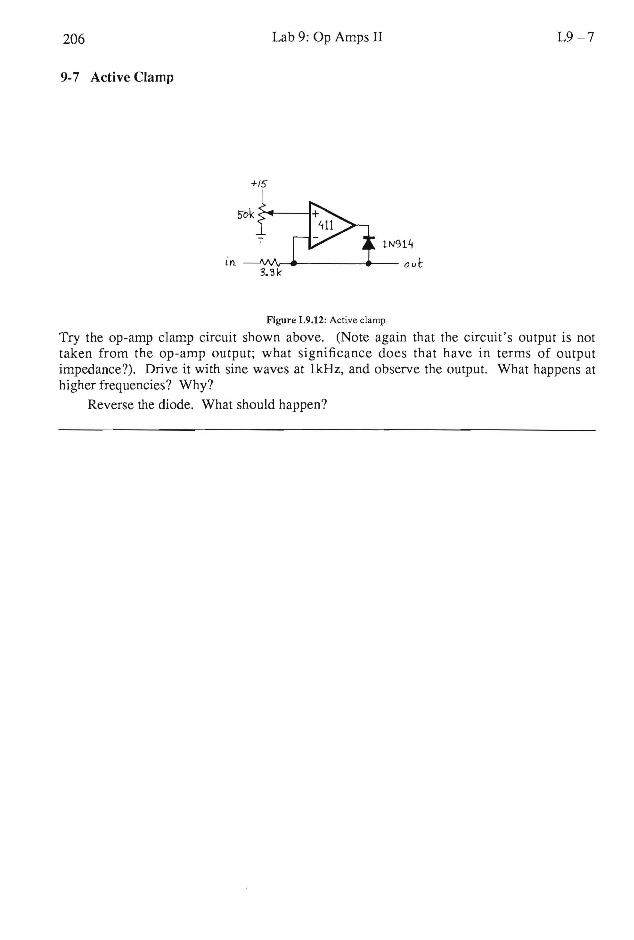