Embed Size (px)
Citation preview
�
STUD
SING
BOO
M.P. A
SHUB
�
�
�
DeparNatio
�
DY OF
GLE PH
OST CO
AVISEK (
BHAM (10
rtment onal Insti
INPUT
HASE A
ONVERT
(109EE02
09EE0561
�
of Electriitute of T
T POWE
AC-DC C
TER
270)
1)
ical EngTechnolo
�
ER FAC
CIRCU
gineeringogy Rour
CTOR C
UIT USI
grkela
CORRE
ING PA
ECTIO
ARALLE
N IN
EL
�
STU
SIN
A T
UDY OF
NGLE P
Thesis subm
Ba
F INPUT
PHASE
B
mitted in p
achelor of
DepartNatio
Ro
T POW
AC-DC
BOOST
partial fulf
f Technolog
M.P. AV
SHUBH
Und
Prof
tment ofonal Insourkela-
M
WER FA
C CIRC
T CONV
fillment of
gy in “Ele
By
VISEK (10
HAM (109
der guidan
f. A.K. PA
f Electristitute o-769008May-20
ACTOR
CUIT US
VERTE
f the requir
ectrical E
09EE0270
9EE0561)
nce of
ANDA
cal Engof Techn8 (ODIS13
CORR
SING P
ER
rements fo
Engineeri
0)
ineeringnologySHA)
RECTIO
PARALL
or the degr
ing”
g
ON IN
LEL
ree of

�
�
This is
Phase A
No. 1O
requirem
session
work ca
The can
The Th
degree/d
In my o
in Electr
Place: R
Dept. ofNationaRourke
to certify th
AC-DC Cir
O9EE0270)
ments for t
2012-2013
arried out by
ndidates hav
hesis which
diploma.
pinion, the
rical Engine
Rourkela
f Electricalal institute ela-769008
C
hat the thes
rcuit Using
and SHU
the award o
at National
y them unde
ve fulfilled a
is based o
thesis is of
eering.
l Engineerinof Technol
NATION
CERT
sis entitled “
g Parallel B
UBHAM (R
of Bachelo
l Institute of
er my superv
all the prescr
on candidat
standard req
ng ogy
DEPARTM
NAL INSTI
TIFIC
“Study of I
Boost Conv
Roll. No.
or of Tech
f Technolog
vision and g
ribed requir
tes’ own w
quired for th
MENT OF
ITUTE OF
CAT
Input Powe
erter”, subm
109EE0561
hnology in
gy, Rourkel
guidance.
rements.
work, have
he award of
ELECTRIC
TECHNOL
ODIS
E
er Factor C
mitted by M
1) in partia
Electrical
a. A bonafi
not submit
f a bachelor
P
CAL ENGIN
LOGY, ROU
SHA, INDIA
Correction
M.P. AVISE
al fulfilmen
Engineerin
ide record o
tted elsewh
of technolo
Prof. A.K. P Profess
NEERING
URKELA
A-769008
in Single
EK (Roll.
nt of the
ng during
of research
here for a
ogy degree
PANDA sor
i
ABSTRACT
An ac to dc converter is t h e m o s t i m p o r t a n t p a r t o f any power supply unit used
in the all- electronic equipments that forms a considerable part of load on the utility. Power
electronic equipments are increasingly being used for power conversion, thereby injecting lower
order harmonics into the utility. As a result, the total harmonic distortion is high and input power
factor is poor. Thus, power factor correction schemes are implemented so as to make the power factor
unity thereby leading to low input current distortion. Amongst the several techniques used for PFC,
high frequency active PFC is used to get better power factor but it has drawbacks that includes
additional losses, thus reducing the overall efficiency, increase in EMI. The efficiency is improved
by reducing the losses using soft switching techniques such as ZVS and ZCS. Boost converter is
preferred because input current does not have cross-over distortion and it is continuous. In this
project, a control technique for boost converter is proposed. This is based on hysteresis-control scheme
in which two sinusoidal current references are generated namely IP,ref, IV,ref, such that one is for the peak
and the other is for the valley of the inductor current. In this control technique, when the inductor
current goes below the lower reference IV,ref the switch is turned on and is turned off when the inductor
current goes above the upper reference IP,ref, thereby giving rise to a variable frequency control. To avoid
too high switching frequency, the switch should be kept open near the zero crossing of the line voltage
so introducing dead times in the line current. Thus, we can say that by using hysteresis controlled boost
converter PFC , power factor of an AC-DC converter can be increased.

ii
ACKNOWLEDGMENT
We would like to articulate our deep gratitude to our project guide Prof. A.K. PANDA who
has always been source of motivation and firm support for carrying out the project. We would
also like to convey our sincerest gratitude and indebtedness to all other faculty members and
staff of Department of Electrical Engineering, NIT Rourkela, who showed their great
efforts and guidance at required times without which it would have been very difficult to
carry out our project work. Moreover, an assemblage of this nature could never have
been attempted with our reference to the works of others whose details are mentioned in the
references section at the last. We acknowledge our indebtedness to all of them. Furthermore,
we would like to t ake name o f our parents and God who directly or indirectly encouraged
and motivated us during this dissertation.
iii
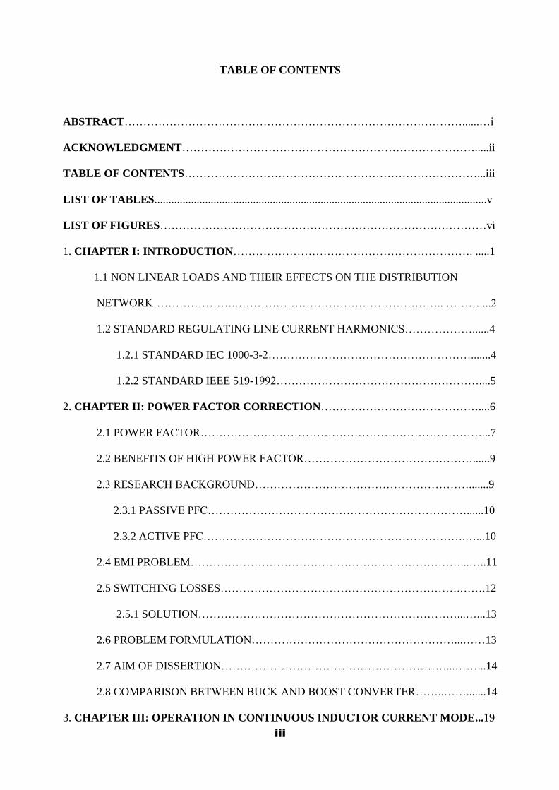
TABLE OF CONTENTS
ABSTRACT………………………………………………………………………………......…i
ACKNOWLEDGMENT…………………………………………………………………….....ii
TABLE OF CONTENTS……………………………………………………………………...iii
LIST OF TABLES......................................................................................................................v
LIST OF FIGURES……………………………………………………………………………vi
1. CHAPTER I: INTRODUCTION………………………………………………………. .....1
1.1 NON LINEAR LOADS AND THEIR EFFECTS ON THE DISTRIBUTION
NETWORK………………….……………………………………………….. ………....2
1.2 STANDARD REGULATING LINE CURRENT HARMONICS………………......4
1.2.1 STANDARD IEC 1000-3-2……………………………………………….......4
1.2.2 STANDARD IEEE 519-1992………………………………………………....5
2. CHAPTER II: POWER FACTOR CORRECTION……………………………………....6
2.1 POWER FACTOR…………………………………………………………………...7
2.2 BENEFITS OF HIGH POWER FACTOR………………………………………......9
2.3 RESEARCH BACKGROUND………………………………………………….......9
2.3.1 PASSIVE PFC……………………………………………………………......10
2.3.2 ACTIVE PFC…………………………………………………………….…...10
2.4 EMI PROBLEM………………………………………………………………...…..11
2.5 SWITCHING LOSSES……………………………………………………….…….12
2.5.1 SOLUTION……………………………………………………………...…...13
2.6 PROBLEM FORMULATION………………………………………………...……13
2.7 AIM OF DISSERTION……………………………………………………...……...14
2.8 COMPARISON BETWEEN BUCK AND BOOST CONVERTER……..…….......14
3. CHAPTER III: OPERATION IN CONTINUOUS INDUCTOR CURRENT MODE...19
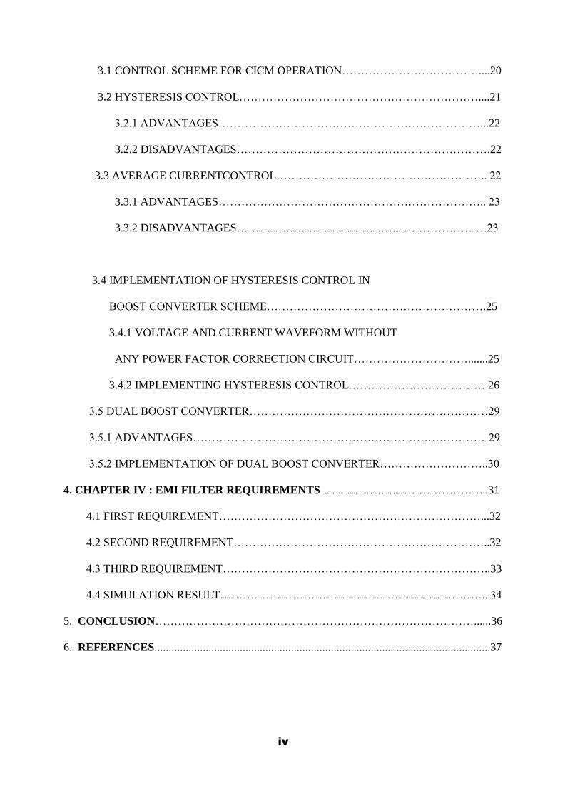
iv
3.1 CONTROL SCHEME FOR CICM OPERATION………………………………....20
3.2 HYSTERESIS CONTROL………………………………………………………....21
3.2.1 ADVANTAGES……………………………………………………………...22
3.2.2 DISADVANTAGES………………………………………………………….22
3.3 AVERAGE CURRENTCONTROL……………………………………………….. 22
3.3.1 ADVANTAGES…………………………………………………………….. 23
3.3.2 DISADVANTAGES…………………………………………………………23
3.4 IMPLEMENTATION OF HYSTERESIS CONTROL IN
BOOST CONVERTER SCHEME………………………………………………….25
3.4.1 VOLTAGE AND CURRENT WAVEFORM WITHOUT
ANY POWER FACTOR CORRECTION CIRCUIT………………………….......25
3.4.2 IMPLEMENTING HYSTERESIS CONTROL……………………………… 26
3.5 DUAL BOOST CONVERTER………………………………………………………29
3.5.1 ADVANTAGES……………………………………………………………………29
3.5.2 IMPLEMENTATION OF DUAL BOOST CONVERTER………………………..30
4. CHAPTER IV : EMI FILTER REQUIREMENTS……………………………………...31
4.1 FIRST REQUIREMENT……………………………………………………………...32
4.2 SECOND REQUIREMENT…………………………………………………………..32
4.3 THIRD REQUIREMENT……………………………………………………………..33
4.4 SIMULATION RESULT……………………………………………………………...34
5. CONCLUSION…………………………………………………………………………......36
6. REFERENCES......................................................................................................................37

v
LIST OF TABLES
1.1 ODD HARMONIC CONTROL……………………………………………………….,…...5
vi
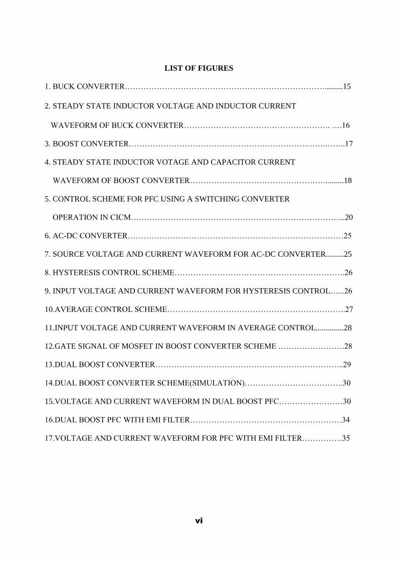
LIST OF FIGURES
1. BUCK CONVERTER………………………………………………………………….........15
2. STEADY STATE INDUCTOR VOLTAGE AND INDUCTOR CURRENT
WAVEFORM OF BUCK CONVERTER………………………………………………. ….16
3. BOOST CONVERTER………………………………………………………….…….……..17
4. STEADY STATE INDUCTOR VOTAGE AND CAPACITOR CURRENT
WAVEFORM OF BOOST CONVERTER…………………………………………….........18
5. CONTROL SCHEME FOR PFC USING A SWITCHING CONVERTER
OPERATION IN CICM……………………………………………………………………...20
6. AC-DC CONVERTER………………………………………………………………………25
7. SOURCE VOLTAGE AND CURRENT WAVEFORM FOR AC-DC CONVERTER.........25
8. HYSTERESIS CONTROL SCHEME……………………………………………………….26
9. INPUT VOLTAGE AND CURRENT WAVEFORM FOR HYSTERESIS CONTROL…...26
10.AVERAGE CONTROL SCHEME………………………………………………………….27
11.INPUT VOLTAGE AND CURRENT WAVEFORM IN AVERAGE CONTROL..............28
12.GATE SIGNAL OF MOSFET IN BOOST CONVERTER SCHEME …………………….28
13.DUAL BOOST CONVERTER……………………………………………………………..29
14.DUAL BOOST CONVERTER SCHEME(SIMULATION)……………………………….30
15.VOLTAGE AND CURRENT WAVEFORM IN DUAL BOOST PFC……………………30
16.DUAL BOOST PFC WITH EMI FILTER…………………………………………………34
17.VOLTAGE AND CURRENT WAVEFORM FOR PFC WITH EMI FILTER……………35

1
CHAPTER 1
Introduction
2
1.Introduction
Most applications compris ing of ac-dc power converters need the output dc voltage to be
well regulated with good steady-state as we l l a s transient performance. The circuit which
was typically favoured until recently (diode rectifier-capacitor filter) for the utility interface
minimizes the cost, but it severely deteriorates the quality of the supply thereby affecting the
performance of other loads connected to it also causing other well-known problems.
Furthermore, in order to maintain the quality of the utility supply, several national and
international agencies have decided imposing standards along with recommendations for
electronic instruments connected to the system. Since the mid-1980's power electronics
engineers have always tried to develop new approaches for better utility interface, to meet the
above mentioned standards. These new circuits have been collectively known as Power factor
correction (PFC) circuits.
With the increase of consumer electronics in the system the power quality becomes poor.
The reactive power drawn from the supply is increasing. This is as a result of the use of
rectification of the AC input in addition to the use of a bulk capacitor directly after the diode
bridge rectifier so as to reduce the input current harmonics to meet the agency standards that
implies improvement of power factor as well. For this reason the publications that are
reported in this area have used "Power factor correction methods" and "Harmonic
elimination/reduction methods" almost inter changeably well. Several techniques for PFC and
harmonic reduction have been reported and a few of them have gained greater acceptance
over the others.
This chapter discusses the i) Nonlinear loads and their effect on the electricity distribution
network, ii) Standard IEC and IEEE regulation for harmonics, iii) Power factor correction
and its benefits, iv) application of PFC both for linear and non-linear loads, v) research
background, vi) problem formulation, and vii) aim of the dissertation.
1.1 NON LINEAR LOADS AND THEIR EFFECTS ON THE DISTRIBUTION
NETWORK:
The instrument connected to an electricity distribution network usually needs some kind of
power conditioning, typically rectification, which produces a non-sinusoidal line current due to
the non-linear input characteristic.

3
Line-frequency diode rectifiers convert AC input voltage into DC output voltage in an
uncontrolled manner. Single-phase diode rectifiers can be used for relatively low power
instrument that needs some kind of power conditioning, such as electronic instrument and
household appliances. For higher power, three-phase diode rectifiers are used. In both single
and three-phase rectifiers, Across the rectifier output a large filtering capacitor is connected to
obtain DC output voltage with low ripple content. Thus, the line current becomes non
sinusoidal. In most of these cases, the amplitude of odd harmonics of the line current is
considerable with respect to the fundamental. While the effect of a single low power
nonlinear load on the network can be considered negligible, the cumulative effect of several
nonlinear loads is important. Line current harmonics have a number of undesirable effects on
both the distribution network and consumers. These effects include:
Increased losses and overheating in transformers, shunt capacitors, power cables, AC
machines and Switchgear, thereby leading to premature aging and failure.
It leads to excessive current in the neutral conductor of three-phase four-wire systems,
caused by odd Triplent current harmonics ( 3rd, 9th, 15th, etc.).
It results in reduced power factor, hence less active power available from a wall
outlet having a certain apparent power rating.
There can be electrical resonances in the power system, leading to excessive peak
voltages and RMS.
High magnitude of currents thereby causing premature aging and failure of capacitors
and insulation.
Other consumers might get affected from the distorted line voltage waveform
connected to the electricity distribution network.
It causes Telephonic interference.
There can be errors in metering instrument.
Increased audio noise.
It also leads to Cogging or Crawling in induction motors, as wel l as mechanical
oscillations in a turbine-generator combination or in a motor-load system.
There can be distortion of the line voltage via the line impedance. The effect is
stronger in weaker grids. For example, some electronic instrument is dependent on the
accurate determination of the voltage wave shape, such as its amplitude, RMS and zero-
crossings.

4
1.2 STANDARDS REGULATING LINE CURRENT HARMONICS :
1.2.1 STANDARD IEC 1000-3-2:
1. It applies to instrument with a rated current up to and including 16Arms per phase which is
to be connected to 50Hzor 60 Hz, 220-240Vrms single-phase or 380-415Vrms three- phase
mains.
2. Items of electrical instruments are categorized into four classes (A,B,C and D), for which
specific limits are set for the harmonic content of the line current.
3. These limits do not apply for the instrument with rated power less than 75W , other than
lighting instrument.
CLASS-A:
Instrument not specified in one of the other three classes should be considered as class-A
instrument.
CLASS-B:
It includes portable tools, and nonprofessional arc welding instrument.
CLASS-C:
It includes lighting instrument (except for dimmers for incandescent lamps, which belong
to class-A).
CLASS-D:
Instrument with special line current shape i.e. includes instrument having an active
input power less than or equal to 600W, and can be of the following types:
i. Personal computers.
ii. Personal computer monitors. iii. Television receivers.
5
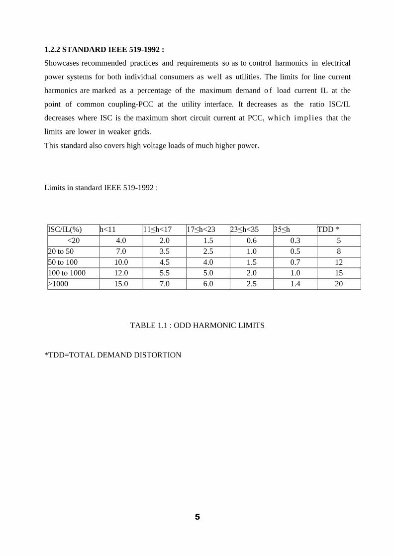
1.2.2 STANDARD IEEE 519-1992 :
Showcases recommended practices and requirements so as to control harmonics in electrical
power systems for both individual consumers as well as utilities. The limits for line current
harmonics are marked as a percentage of the maximum demand o f load current IL at the
point of common coupling-PCC at the utility interface. It decreases as the ratio ISC/IL
decreases where ISC is the maximum short circuit current at PCC, which implies that the
limits are lower in weaker grids.
This standard also covers high voltage loads of much higher power.
Limits in standard IEEE 519-1992 :
ISC/IL(%) h<11 11≤h<17 17≤h<23 23≤h<35 35≤h TDD *
<20 4.0 2.0 1.5 0.6 0.3 5
20 to 50 7.0 3.5 2.5 1.0 0.5 8
50 to 100 10.0 4.5 4.0 1.5 0.7 12
100 to 1000 12.0 5.5 5.0 2.0 1.0 15
>1000 15.0 7.0 6.0 2.5 1.4 20
TABLE 1.1 : ODD HARMONIC LIMITS
*TDD=TOTAL DEMAND DISTORTION

6
CHAPTER 2
Power factor correction
7
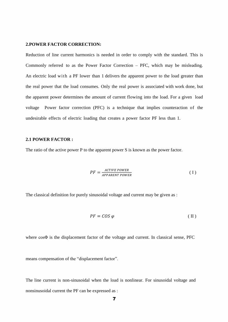
2.POWER FACTOR CORRECTION:
Reduction of line current harmonics is needed in order to comply with the standard. This is
Commonly referred to as the Power Factor Correction – PFC, which may be misleading.
An electric load with a PF lower than 1 delivers the apparent power to the load greater than
the real power that the load consumes. Only the real power is associated with work done, but
the apparent power determines the amount of current flowing into the load. For a given load
voltage Power factor correction (PFC) is a technique that implies counteraction of the
undesirable effects of electric loading that creates a power factor PF less than 1.
2.1 POWER FACTOR :
The ratio of the active power P to the apparent power S is known as the power factor.
( I )
The classical definition for purely sinusoidal voltage and current may be given as :
( II )
where cosΦ is the displacement factor of the voltage and current. In classical sense, PFC
means compensation of the “displacement factor”.
The line current is non-sinusoidal when the load is nonlinear. For sinusoidal voltage and
nonsinusoidal current the PF can be expressed as :
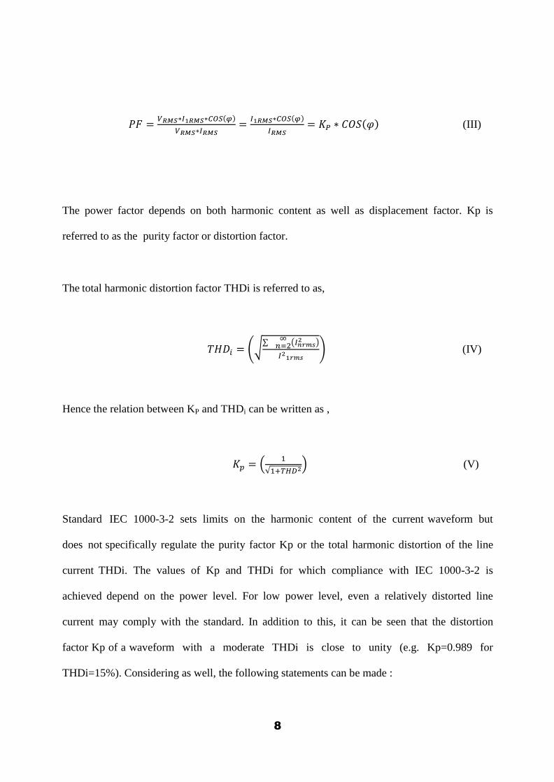
8
( )
( )
( ) (III)
The power factor depends on both harmonic content as well as displacement factor. Kp is
referred to as the purity factor or distortion factor.
The total harmonic distortion factor THDi is referred to as,
(√∑
( )
) (IV)
Hence the relation between KP and THDi can be written as ,
(
√ ) (V)
Standard IEC 1000-3-2 sets limits on the harmonic content of the current waveform but
does not specifically regulate the purity factor Kp or the total harmonic distortion of the line
current THDi. The values of Kp and THDi for which compliance with IEC 1000-3-2 is
achieved depend on the power level. For low power level, even a relatively distorted line
current may comply with the standard. In addition to this, it can be seen that the distortion
factor Kp of a waveform with a moderate THDi is close to unity (e.g. Kp=0.989 for
THDi=15%). Considering as well, the following statements can be made :

9
Power factor PF is not considerably degraded by harmonics, unless their amplitude is
quite large (low Kp, very large THDi).
Low harmonic content in the waveform does not guarantee high power factor (Kp is
close to unity, but low cosΦ).
2.2 BENEFITS OF HIGH POWER FACTOR :
Voltage distortion in the waveform is considerably reduced.
All the power becomes active that is capable of doing work.
Smaller RMS current.
Higher number of loads can be fed from the same power.
2.3 RESEARCH BACKGROUND:
Most of the research on PFC for nonlinear loads is actually meant to concent ra te on
the reduction of the harmonic content of the line current. There are many solutions to achieve
PFC By using a combination of low pass input and output filters, the shape of the input
current can be further improved .Depending on whether active switches (controllable by an
external control input) are used or not, PFC solutions can be categorized as “Passive” or
“Active”.In passive PFC, only passive elements along with the diode bridge rectifier are used,
to improve the shape of the line current waveform. Obviously, the output voltage is not
controllable. For active PFC, active switches are used in conjunction with reactive
elements in order to increase the effectiveness of the line current shaping and to obtain
controllable output voltage. The switching frequency further classifies the active PFC
solutions into two classes. In low frequency active PFC, switching should take place at low-
order harmonics of the line-frequency such that it is synchronized with the line voltage. In
10
high-frequency active PFC, the switching frequency should be much higher than the line
frequency.
2.3.1 Passive PFC
In Passive PFC circuit only passive elements are used along with the diode bridge rectifier, so
as to improve the shape of the line current. In order to improve the shape of the line current
Passive Power Factor correction circuit simply uses an inductor in the input circuits. The
shape of the input current can be further improved by using a combination of low pass input
and output filters. To maintain the flow of input current, voltage doublers is inserted to feed
the valley fill circuit. Even though line current harmonics are reduced, the fundamental
component may suffer an excessive phase shift thereby reducing the power factor. Better
characteristics can be obtained by using “Active PFC”.
2.3.2 Active PFC
Active power factor correction can be accomplished by many ways. The Boost converter
operated on the rectified output uses a constant switching frequency PWM and DCM
operation reduces the total harmonic distortion of the input current .In a Boost circuit the
switching device can handles only a portion of output power which increases the efficiency.
The efficiency can be increased by keeping the ratio of output voltage to input voltage closer
to unity. The effect of second harmonic in PWM in reducing third harmonic component in the
input current is established. In this converter the output is varied by varying the duty cycle
keeping the frequency constant. In this, the other converter topologies for a PFC based Sepic
topology are reported in, which allow comparison of converter performance with different
11
control techniques. The advantages of clamped current control include overall simplicity,
relatively low inductive energy storage and stresses on the components, and fixed operating
frequency. Another control method, which allows a better input current waveform, is the
average current control. In Hysteresis control technique, the switch is turned on when the
inductor current goes below the lower reference namely Ivref, and when the inductor current
goes above the upper reference, the switch is turned off result ing in a variable frequency
control. But in Borderline Control approach the switch on-time is held constant during the line
cycle and when the inductor current falls to zero the switch is turned on, Thus the converter
operates at the boundary between Continuous and Discontinuous Inductor Current Mode
(CICM-DICM). The paper presents a new approach for generating reference currents for an
active filter and a static compensator. The purpose of the compensating scheme is to balance
the load, as well as make the power factor at the supply side a desired value. Here a suitable
compensator structure is proposed which tracks the reference currents in a hysteresis band
control scheme.
2.4 EMI PROBLEM:
The converters operating in CICM reduces the line current harmonics, but it has some
drawbacks, such as: 1) it increases the EMI, due to the high-frequency content of the input
current. 2) It introduces additional losses, thus reducing the overall efficiency. However the
high frequency EMI can be eliminated by introducing an EMI filter between AC supply and
diode bridge rectifier were found in various studies. The second requirement for the EMI
filter: the displacement angle Φ must be kept low. The third requirement is related to the
overall stability of the system. It is known that unstable operation may occur due to the
interaction between the EMI filter and the power stage. However the losses are reduced by
inserting an inductor in the series path of the boost rectifier to reduce the di/dt rate during its
12
turn-off. Better characteristics are obtained in Zero Voltage. Transition – ZVT topologies, at
the expense of increased complexity.
2.5 SWITCHING LOSSES:
In active PFC circuit, switching of semiconductor devices normally occurs at high current
levels. Therefore, when switching at high frequencies these converters are associated with
high power dissipation. Also, the higher input and lower output voltages bring about very low
duty cycles. Hence, the high side MOSFET switch should turn on and off in a very short
period of time, which also brings switching losses into picture. The losses due to switching
produce three considerable effects on the converters in general,
Achievable fs and efficiency limited.
EMI at high frequencies due to high di/dt, dv/dt and induces noise.
Switching losses may sometimes exceed safe operating area.
Switching loss of a MOSFET can be represented mathematically as,
(
) (VI)
From above equation some important result can be deduced that switching losses can be
reduced by two methods:
We can reduce the turn-on and turn-off delay times, by using faster and more efficient
13
switches in the converter.
Before turning it on or off, make the current or voltage across the switch zero. Soft switching
resonant converters are based on this concept.
The switching losses at higher frequencies can be eliminated by the soft switching techniques
available.
2.5.1 SOLUTION :
There are mainly two techniques to eliminate the switching losses namely ZVS and ZCS.In
both techniques, the switching losses in the semiconductor devices are eliminated due to the
fact that current through or voltage across the switching device at the switching point is nearly
or e q u a l t o zero. This reduction in the switching loss allows the designer to attain a
higher operating frequency without sacrificing converter efficiency. By doing so, the
resonant converters show promise of achieving what could not be achieved by the PWM
converter that is the design of small size and weight converters. Currently, resonant power
converters operating in the range of a few megahertz are available. Another advantage of
resonant converters over PWM converters is the decrease of harmonic content in the converter
voltage and current waveforms. Therefore, when the resonant and PWM converters are
operated at the same frequency and power level , it is expected that harmonic emission will be
lower in case of resonant converter.
2.6 PROBLEM FORMULATION:
The investigation of PFC faces the following problems:
High power factor with low efficiency.
High efficiency with low power factor.
14
2.7 AIM OF THIS DISSERTATION:
To better define the scope of the research reported in this dissertation, the PFC is performed
by a high frequency switching DC/DC converter that can shape the input current so close
to a Sinusoidal waveform that is in phase with the line voltage. Thus, from the electrical
point of view, the instrument connected to the line behaves like a resistive load. The high-
frequency switching PFC stage reduces the line current harmonics, but it also has drawbacks,
such as: it introduces additional losses, thereby reducing the overall efficiency; it increases
the EMI, due to the high-frequency content of the input current; and it increases the complexity
of the circuit, with negative effects on the reliability of the instrument, as well as on its size,
weight and cost. The general aim of this dissertation is to investigate high- frequency
switching circuit topologies and different types of methods that can be applied in the PFC
stage, which would alleviate some of the aforementioned drawbacks.
2.8 COMPARISON BETWEEN BOOST AND BUCK CONVERTER:
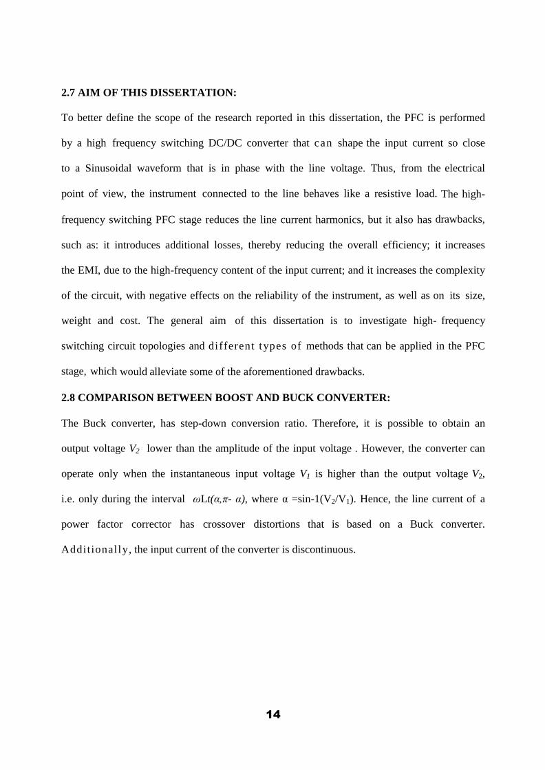
The Buck converter, has step-down conversion ratio. Therefore, it is possible to obtain an
output voltage V2 lower than the amplitude of the input voltage . However, the converter can
operate only when the instantaneous input voltage V1 is higher than the output voltage V2,
i.e. only during the interval ωLt(α,π- α), where α =sin-1(V2/V1). Hence, the line current of a
power factor corrector has crossover distortions that is based on a Buck converter.
Additionally, the input current of the converter is discontinuous.
15
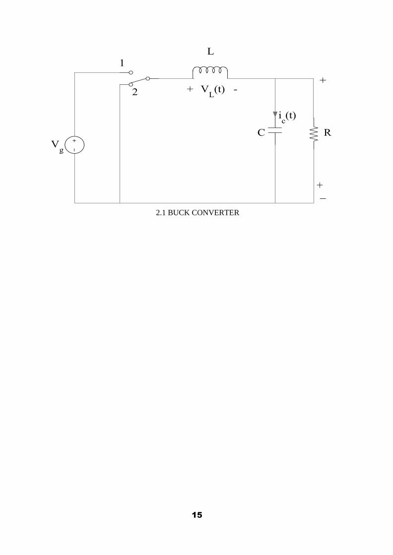
2.1 BUCK CONVERTER
16
2.2 STEADY STATE INDUCTOR VOLTAGE AND CURRENT WAVEFORM OF BUCK
CONVERTER
17
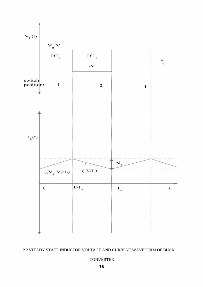
Whereas the Boost converter has a step-up conversion ratio; hence the output voltage V2 is
always higher than the magnitude V1 of the input voltage. Operation is possible throughout
the line-cycle so the input current does not have crossover distortions. Since the inductor is
placed in series at the input, the input current is continuous. Hence, an input current with
reduced high-frequency content can be obtained when continuous conduction mode is in
operation. For these reasons, the Boost converter is widely used for PFC.
2.3 BOOST CONVERTER
18
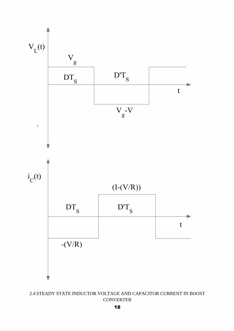
2.4 STEADY STATE INDUCTOR VOLTAGE AND CAPACITOR CURRENT IN BOOST
CONVERTER

19
CHAPTER 3
Operation in CICM
HYSTERESIS CONTROL
AVERAGE CURRENT CONTROL
20
3.OPERATION IN CONTINUOUS INDUCTOR CURRENT MODE(CICM)
In this operating mode, the inductor current never reaches zero during one switching
cycle and there is always energy stored in the inductor.
3.1 CONTROL SCHEME FOR CICM OPERATION:
The volt-seconds applied to the inductor must be balanced throughout the line-cycle by
continuously changing the duty-cycle of the converter using an appropriate control method.
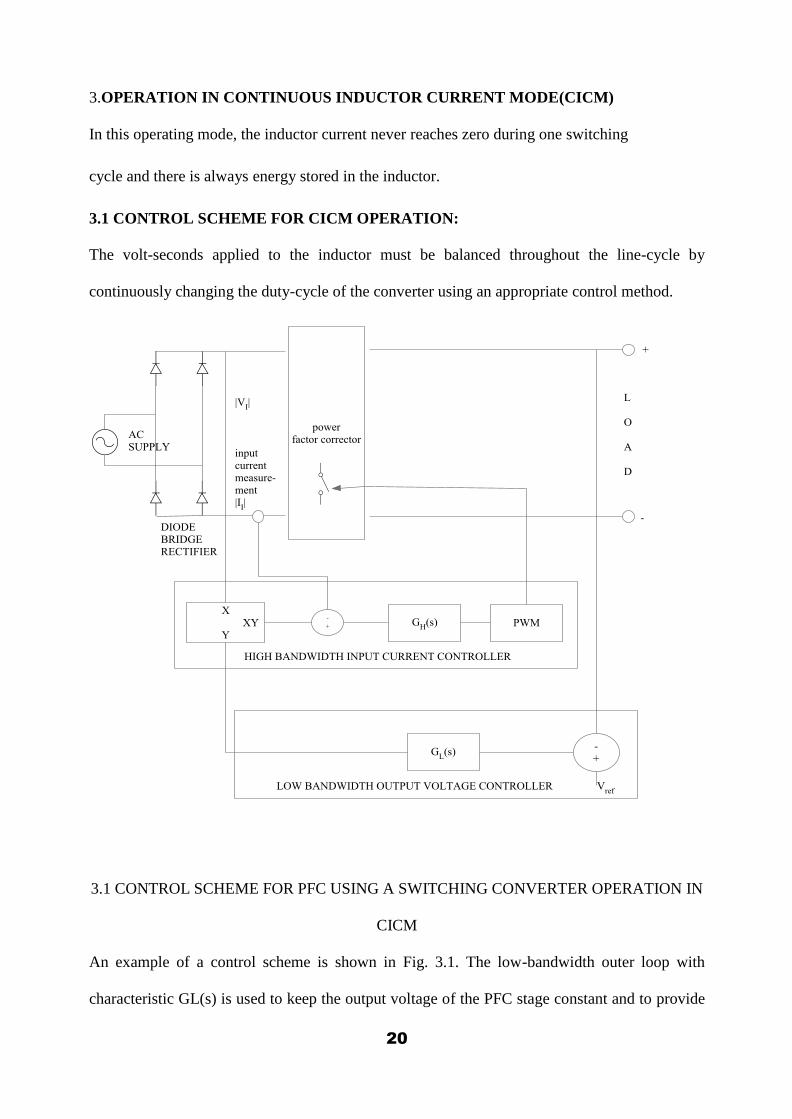
3.1 CONTROL SCHEME FOR PFC USING A SWITCHING CONVERTER OPERATION IN
CICM
An example of a control scheme is shown in Fig. 3.1. The low-bandwidth outer loop with
characteristic GL(s) is used to keep the output voltage of the PFC stage constant and to provide
21
the error signal Vε. The high-bandwidth inner loop with characteristic GH(s) is used to control
the input current. A multiplier is used to provide a reference Vxy, which is proportional to the
error signal Vε and which has a modulating signal with the desired shape for the input current.
Fig. 3.1 shows the most common situation, where the modulating signal is the rectified-sinusoid
input voltage V1. Depending on the topology of the PFC stage, it may be beneficial to use as a
modulating signal the difference between the input voltage and the output voltage. The control
circuit can be simplified by eliminating the multiplier and the sensing of the line voltage. In this
case the modulating signal is Vxy = Vε, and it is essentially constant over the line cycle, because
Vε is the control signal from the low-bandwidth output voltage controller. Therefore, the input
current is clamped to a value proportional with Vε and its shape approaches a square waveform.
The simplification of the control circuit leads to a more distorted line current, but compliance
with the standard can be obtained up to approximately 500W for a 230Vrms input voltage.
Furthermore, if the edges of the line current waveform are softened, thus obtaining a nearly
trapezoidal waveform, compliance up to several kW can be obtained. There are several ways to
implement the high-bandwidth inner loop. Some of them are:
Peak current control.
Average current control.
Hysteresis control.
Borderline control.
Even though these control techniques can be used for all DC-DC converters, only boost
converter has been taken for the study because of the continuous input current.
3.2 HYSTERASIS CONTROL:
In this type of control two sinusoidal current references IV,ref, IP,ref are generated as shown in Fig
3.2, one is for the valley and the other for the peak of the inductor current. According to this
control technique, when the inductor current goes below the lower reference IV,ref the switch is
22
turned on and when the inductor current goes above the upper reference IP,ref the switch is
turned off giving rise to a variable frequency control. The switch can be kept open near the zero
crossing of the line voltage so introducing dead times in the line current in order to avoid the
switching frequency too high.
3.2.1 ADVANTAGES:
No need of compensation ramp.
Low distorted input current waveforms.
3.2.2 DISADVANTAGES:
Variable switching frequency.
Inductor current must be sensed.
Control sensitive to commutation noises.
3.3 AVERAGE CURRENT CONTROL SCHEME :-
Another control method, which allows a better input current waveform, is the average current
control. Here the inductor current is sensed and filtered by a current error amplifier whose
output drives a PWM modulator. In this way the inner current loop tends to reduce the error
between the average input current ig and its reference. The same is obtained in the peak current
control. The converter works in CICM, so with regard to the peak current control the same
considerations can be applied. The technique of average current mode control overcomes the
demerit of peak current control mode by introducing a high gain integrating current error
amplifier (CA) into the current loop. For optimum performance, the gain-bandwidth
characteristic of the current loop can be tailored by the compensation network around the CA.

23
The current loop gain crossover frequency fc can be made approximately the same as compared
with the peak current mode control, but the gain will be much greater at lower frequencies.
The result is:
1. Average current tracks the current program with a high degree of accuracy. This is especially
important in high power factor pre-regulators, enabling less than 3% harmonic distortion to be
achieved with a relatively small inductor. In fact, average current mode control functions well
even when the mode boundary at low current levels is crossed into the discontinuous mode To
this mode change, the outer voltage control loop is oblivious.
2. Slope compensation is not required, but in order to achieve stability at the switching
frequency, there is a limit to loop gain.
3. Noise immunity is excellent. The oscillator ramp immediately dives to its lowest level when
the clock pulse turns the power switch on, at the input of the PWM comparator volts away from
the corresponding current error level.
4. The average current mode method can be used to control and sense the current in any circuit
branch. Thus input current can be controlled accurately with flyback and buck topologies, and
can control output current with boost and flyback topologies.
3.3.1 Advantages:
1. Constant switching frequency;
2. No need of compensation ramp;
3. Due to current filtering, control is less sensitive to commutation noises;
4. Better input current waveforms than that in case of peak current control since, the duty cycle
is close to one near the zero crossing of the line voltage.
3.3.2 Disadvantages:
1. Inductor current must be sensed;

24
2. A current error amplifier is needed and its compensation network design must take into
account the different converter operating points during the line cycle.
Many control IC's are available from different manufacturers: UC1854/A/B family (Unitrode),
UC1855 (Unitrode), TK3854A (Toko), ML4821 (Micro Linear), TDA4815, TDA4819
(Siemens), TA8310 (Toshiba), L4981A/B (SGS-Thomson), LT1248, LT1249 (Linear
Technology).
25
3.4 IMPLEMENTATION OF HYSTERESIS CONTROL IN BOOST CONVERTER
SCHEME:
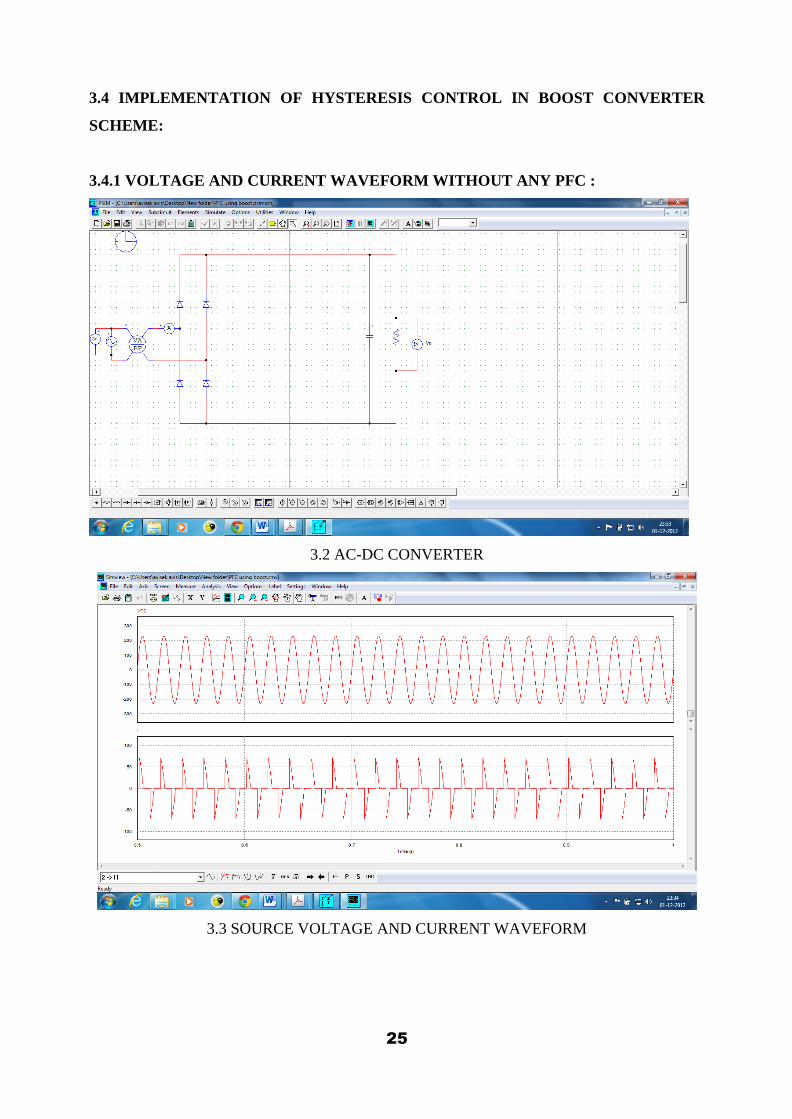
3.4.1 VOLTAGE AND CURRENT WAVEFORM WITHOUT ANY PFC :
3.2 AC-DC CONVERTER
3.3 SOURCE VOLTAGE AND CURRENT WAVEFORM
26
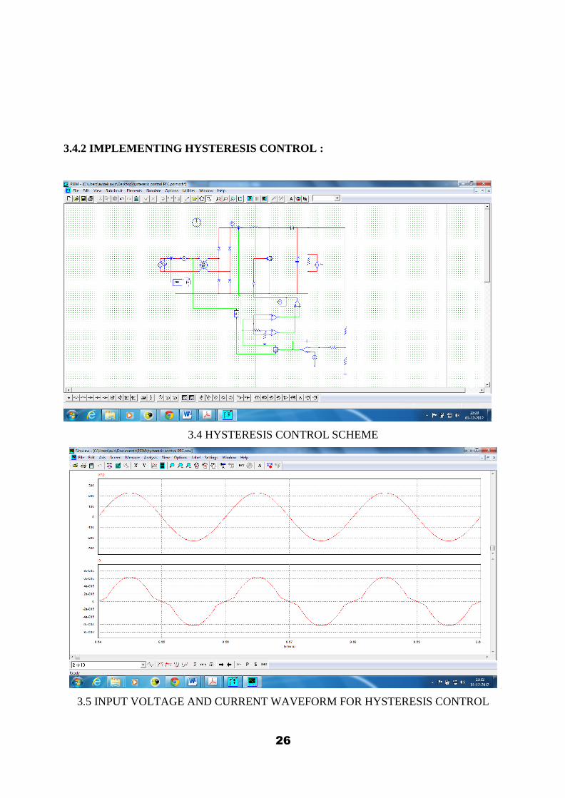
3.4.2 IMPLEMENTING HYSTERESIS CONTROL :
3.4 HYSTERESIS CONTROL SCHEME
3.5 INPUT VOLTAGE AND CURRENT WAVEFORM FOR HYSTERESIS CONTROL
27
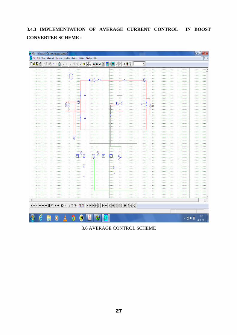
3.4.3 IMPLEMENTATION OF AVERAGE CURRENT CONTROL IN BOOST
CONVERTER SCHEME :-
3.6 AVERAGE CONTROL SCHEME
28
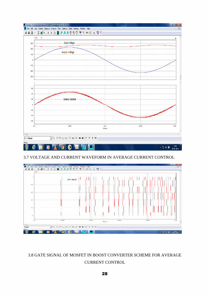
3.7 VOLTAGE AND CURRENT WAVEFORM IN AVERAGE CURRENT CONTROL
3.8 GATE SIGNAL OF MOSFET IN BOOST CONVERTER SCHEME FOR AVERAGE
CURRENT CONTROL

29
3.5 DUAL BOOST CONVERTER:
First boost converters are used as active Power factor correctors but recently dual boost
converter have taken the place of boost converters in design of PFC i.e. two boost converters
connected in parallel. Circuit diagram of dual boost PFC is shown below:
3.9 dual boost converter
Here, we use a parallel boost scheme, where inductor Lb1 and switch(mosfet) Tb1 are for main
PFC while Lb2(inductor) and Tb2(switch) are for active filtering. This dual boost circuit serves
two purposes i.e. reduces the PFC total switching loss and improves the quality of line
current.Because of different values of switching frequency and current amplitude for the two
switches ,the switching losses decreases.
3.5.1ADVANTAGES:
High efficiency
Its modular design leads to reduction of its development cost
Reliability increases
Current ripple decreases
Conduction losses decreases
30
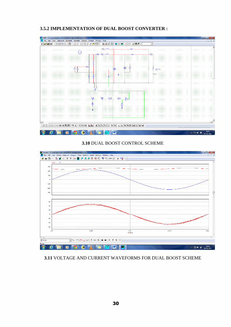
3.5.2 IMPLEMENTATION OF DUAL BOOST CONVERTER :
3.10 DUAL BOOST CONTROL SCHEME
3.11 VOLTAGE AND CURRENT WAVEFORMS FOR DUAL BOOST SCHEME

31
CHAPTER 4
EMI FILTER REQUIREMENTS
32
4. EMI FILTER REQUIREMENTS
The high-frequency ripple of the input current of switching converters generates differential-
mode EMI, while the common-mode EMI is a result of secondary, usually parasitic, effects.
Typically, the differential-mode EMI is dominant below 2MHz, while the common-mode EMI
is considerable above 2MHz .
4.1 One stage LC filter for attenuating differential-mode EMI:
A high-frequency active PFC stage significantly increases the differential-mode EMI, typically
by 30dB to 60dB according to and an EMI filter must be used to comply with EMI standards.
There are three main requirements concerning the design of the EMI filter for a PFC stage First
requirement:
In order to ensure compliance with the EMI standards, the first requirement for the EMI filter is
to provide the required attenuation,
4.2 Second requirement:
We consider the phasor diagram of the line-frequency components of the system currents and
voltages. We assume that the input current ig is sinusoidal and in phase with the input voltage
vg of the PFC stage, assuming that the voltage drop is very small across the filter inductor La at
line-frequency, essentially equal to the line voltage vi . proportional to Ca, A displacement
angle Φ is introduced between the line current Ii and the line voltage Vi due to the capacitive
current IC , which degrades the power factor. This leads to the second requirement for the EMI
filter: the displacement angle Φ must be kept low. Hence, the capacitance Ca that can be used is
upper limited. Ca < Cmax, As a consequence, the inductance La is lower limited La > Lmin In
order to have a product LaCa that gives the required attenuation.
33
4.3 Third requirement:
The third requirement is related to the overall stability of the system. It is known that unstable
operation may occur due to the interaction between the EMI filter and the power stage. This
phenomenon is analyzed in several publications, including for peak current mode controlled
DC/DC converters, and for power factor correctors with average current mode control. To
explain it, let us consider the thevenin equivalent circuit of the EMI filter/PFC stage
interconnection. Hf is the transfer function of the filter, Zof is the output impedance of the EMI
filter and Zic is the input impedance of the PFC stage. Where Tf can be considered as a loop
gain that must satisfy the Nyquist criterion for stability. The interaction is reduced between the
EMI filter and the power converter and thus no instabilities can arise in the system, if |Tf|<<1.
This means that the modulus of the output impedance of the EMI filter must be much lower
than the modulus of the input impedance of the power converter, |Zof|<<|Zic|. The
aforementioned condition may be difficult to fulfill in a PFC application. This is because, the
modulus of the output impedance Zof has a maximum that is proportional to a a L C , at the
resonant frequency of the EMI filter, which cannot be set arbitrarily low since Ca is upper
limited and La is lower limited. Hence, in a PFC application it is possible to have |Tf|>1,
especially at low Zic, i.e. at low line voltage and high load current. Thus, if the input impedance
Zic shows an excessive positive phase shift, then Tf of ic Z may not satisfy the Nyquist
criterion for stability and instabilities occur. For this reason, it is important to know the input
impedance Zic of the PFC stage, in order to be able to perform the stability analysis.
34
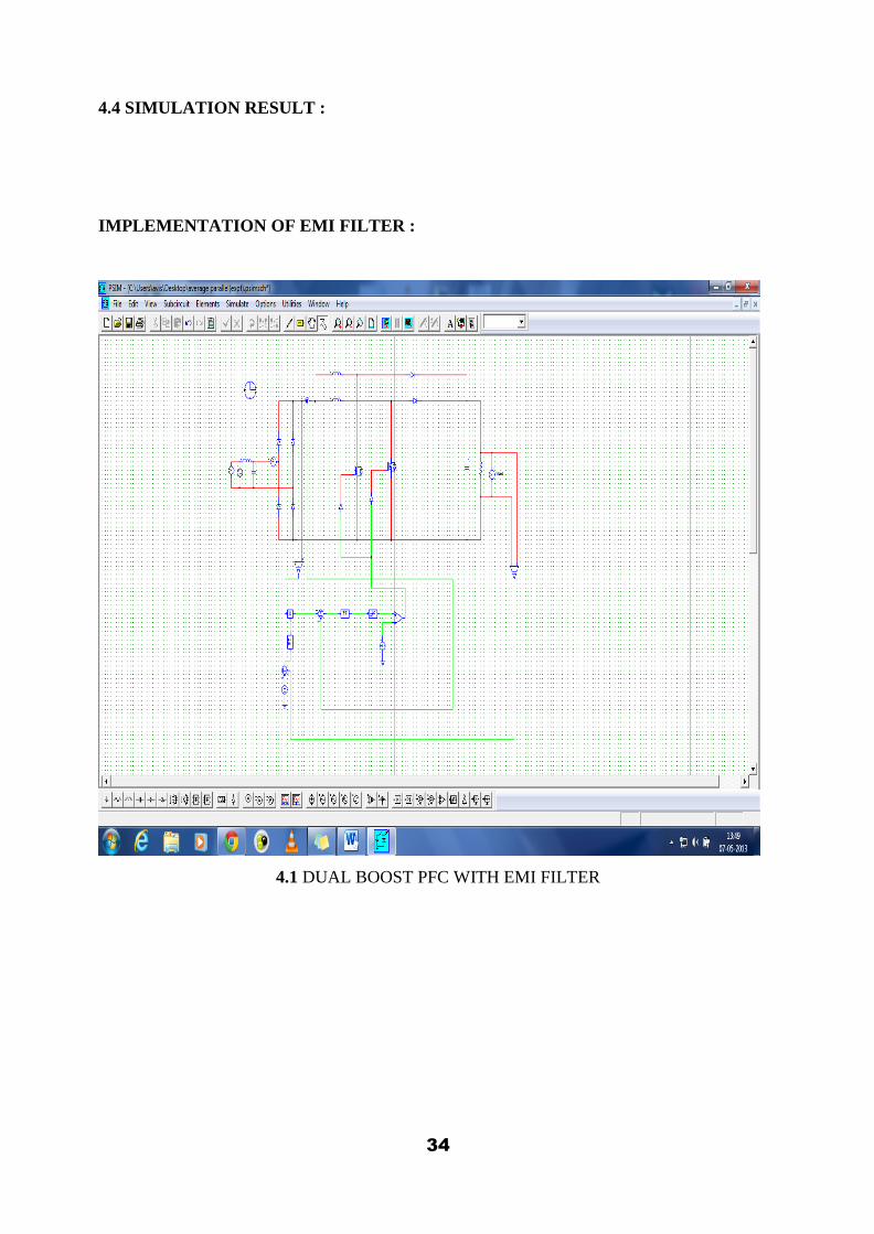
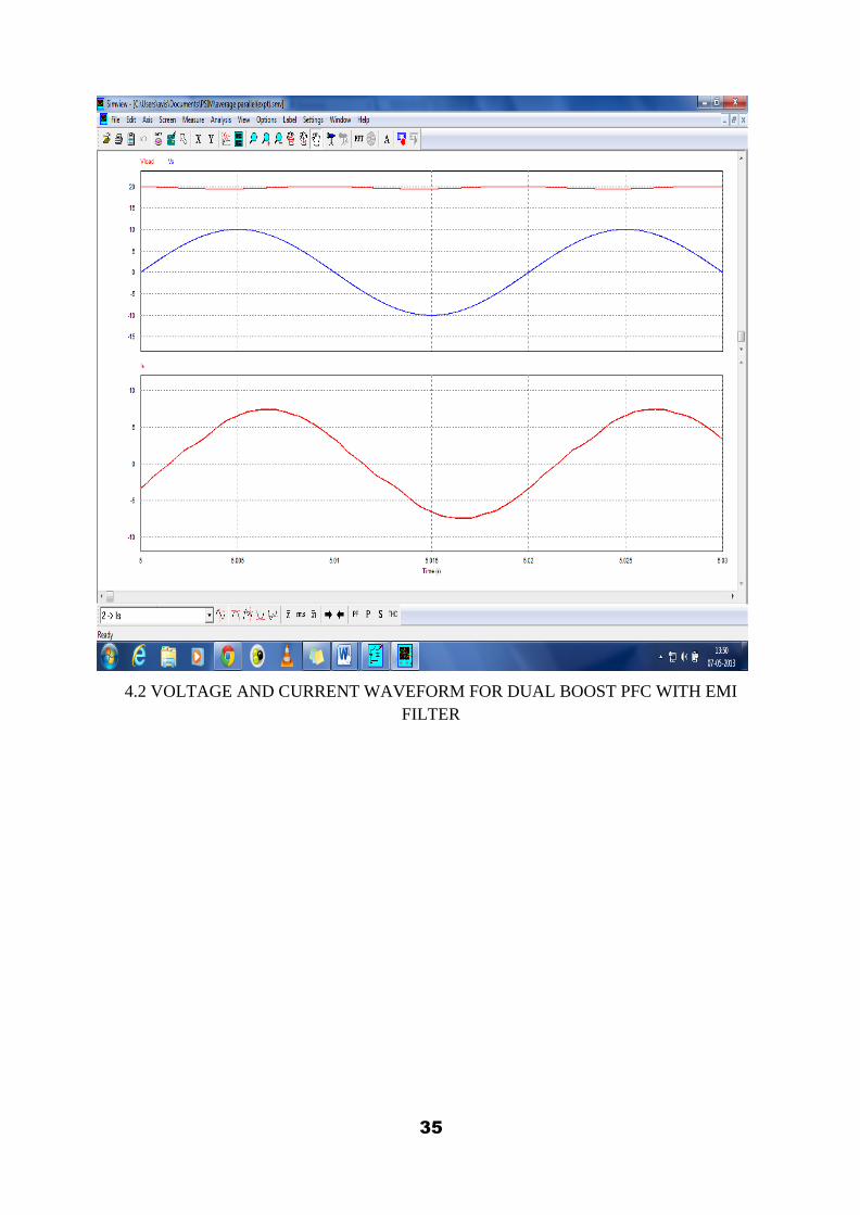
4.4 SIMULATION RESULT :
IMPLEMENTATION OF EMI FILTER :
4.1 DUAL BOOST PFC WITH EMI FILTER
35
4.2 VOLTAGE AND CURRENT WAVEFORM FOR DUAL BOOST PFC WITH EMI
FILTER

36
CONCLUSION:
Thus boost converter is preferred over buck converter in single phase power factor correction
circuit. Boost converter with hysteresis control technique shows higher input power factor
(lower THD).For better input current waveforms and constant switching frequency, we prefer
average current control scheme. Further improvement of power factor has been done by using
parallel boost converter techniques. EMI filter has been added in order to further decrease the
total harmonic distortion. Further improvement can be done by using soft-switching
techniques.
37
REFERENCES :
[1] Fairchild Semiconductor- “Application Note 42047,Power Factor Correction (PFC)
Basics” –www.fairchildsemi.com.
[2] N. Mohan, et el. Power Electronics: Converters, Applications, and Design. New York: NY,
USA, John Wiley & Sons, Inc., 1995.
[3] Kurma Sai Mallika, Prof. A.K.Panda, “Topological issues in single phase power factor
correction” M.Tech thesis at National Intstitute of Technology, Rourkela. (2007).
[4] Redl, Richard, “Reducing distortion in peak-current-controlled boost power factor
correctors.” Proc. of IEEE Applied Power Electronics Conference, APEC’94. (1994): pp. 576-
583.
[5] Lai, J. S., “Design consideration for Power Factor Correction Boost converter Operating at
the Boundary of Continuous Conduction mode and Discontinuous Conduction mode.” Proc. of
IEEE Applied Power Electronics Conference, APEC’93. (1993): pp. 267-273.
[6] Redl, Richard, et el. “Power-Factor Correction with Interleaved Boost Converters in
Continuous-Inductor-Current Mode.” Proc. of IEEE Applied Power Electronics Conference,
APEC’93. (1993): pp.168-174.
38
[7] Wu, M. K. W., et el. “A review of EMI problems in switch mode power supply design.”
Journal of Electrical and Electronics Engineering, Australia. vol. 16, nos. 3&4, (1996): pp. 193-
204.
[8] Redl, Richard, “Power electronics and electromagnetic compatibility.” Proc. of IEEE Power
Electronics Specialists Conference, PESC’96. (1996): pp. 15-21.
[9] Vlatkovic, V., et el. “Input filter design for power factor correction circuits.” IEEE
Transactions on Power Electronics. vol. 11, no. 1, (Jan. 1996): pp. 199-205.
[10] Huma Khan, Prof. A.K.Panda, “Improving the Performance of Single Phase Power Factor
Correction Circuit using Parallel Boost Converters.” B.Tech thesis at National Intstitute of
Technology, Rourkela. (2012).
[11] Parillo,F. , “Dual Boost High performances Power Factor Correction Systems(PFC),”
[12] Wu, M. K. W., et el. “A review of EMI problems in switch mode power supply design.”
Journal of Electrical and Electronics Engineering, Australia. vol. 16, nos. 3&4, (1996): pp. 193-
204.