Embed Size (px)
Citation preview

San Jose State University San Jose State University
SJSU ScholarWorks SJSU ScholarWorks
Master's Theses Master's Theses and Graduate Research
2008
Study of voltage, acid concentration, and temperature on Study of voltage, acid concentration, and temperature on
nanopore structures nanopore structures
Rajvinder S. Virk San Jose State University
Follow this and additional works at: https://scholarworks.sjsu.edu/etd_theses
Recommended Citation Recommended Citation Virk, Rajvinder S., "Study of voltage, acid concentration, and temperature on nanopore structures" (2008). Master's Theses. 3512. DOI: https://doi.org/10.31979/etd.v9mw-b48a https://scholarworks.sjsu.edu/etd_theses/3512
This Thesis is brought to you for free and open access by the Master's Theses and Graduate Research at SJSU ScholarWorks. It has been accepted for inclusion in Master's Theses by an authorized administrator of SJSU ScholarWorks. For more information, please contact [email protected].

STUDY OF VOLTAGE, ACID CONCENTRATION, AND TEMPERATURE ON NANOPORE STRUCTURES
A Thesis
Presented to
The Faculty and Department of Chemical and Materials Engineering
San Jose State University
In Partial Fulfillment
of the Requirements for the Degree
Master of Science
by
Rajvinder S. Virk
August 2008

UMI Number: 1459720
Copyright 2008 by
Virk, Rajvinder S.
All rights reserved.
INFORMATION TO USERS
The quality of this reproduction is dependent upon the quality of the copy
submitted. Broken or indistinct print, colored or poor quality illustrations and
photographs, print bleed-through, substandard margins, and improper
alignment can adversely affect reproduction.
In the unlikely event that the author did not send a complete manuscript
and there are missing pages, these will be noted. Also, if unauthorized
copyright material had to be removed, a note will indicate the deletion.
®
UMI UMI Microform 1459720
Copyright 2008 by ProQuest LLC.
All rights reserved. This microform edition is protected against
unauthorized copying under Title 17, United States Code.
ProQuest LLC 789 E. Eisenhower Parkway
PO Box 1346 Ann Arbor, Ml 48106-1346

©2008
Rajvinder S. Virk
ALL RIGHTS RESERVED

APPROVED FOR THE DEPARTMENT OF CHEMICAE AND MATERIAL ENGINEERING
Dr. Melanie McNeil ' Date Professor College of Engineering Chemical and Materials Department
3/31/0 (, Dr. Stephanie \ Lecturer College of Engineering Chemical and Materials Department
V\U^vffiE$^ M i i i ^ Dr. Meyya Meyyappan Date NASA AMES Research Center Director of Nanotechnology
APPROVED FOR THE UNIVERSITY
"J? / /t'jA^^t* V- •! )/**~^2~-
Date

ABSTRACT
STUDY OF VOLTAGE, ACID CONCENTRATION, AND TEMPERATURE ON NANOPORE STRUCTURES
By Rajvinder S. Virk
Anodization of aluminum is a relatively well-known technique which dates back
several decades. Under appropriate conditions, this electrochemical process produces
nanopores on an aluminum surface. Despite past efforts, the effects of acid electrolyte
solution concentrations and intensity of voltage on nanopore characteristics has not been
reported in detail in literature. In this study, a 500 nanometer (nm) aluminum film is
sputtered upon a prepared silicon substrate, containing a 250 nm titanium sub-layer. This
substrate is electrochemically anodized, chemically etched, and then re-anodized in the
presence of oxalic and phosphoric acid solutions. The effect of simultaneously varying
voltage intensity and the oxalic and phosphoric electrolyte concentrations was explored
by utilizing a design of experiment technique. A subsequent temperature and grain size
study was also conducted. The effect of modifying these parameters was determined by
calculating the change in pore diameter, nanopore density, and a tortuosity values. It was
found that voltage has the greatest effect on influencing the pore density (a decrease of
1.01 E+10 pores/cm ), diameter (an increase of 15.42 nm), and tortuosity (an increase of
13.58%).

AKNOWLEDGEMENTS
This work has been done in cooperation with NASA Ames Nanotechnology
Research Center. The reported experiments and results would not have been possible
without the support and guidance of Dr. Meya Meyappen, Dr. Hou T Ng, and Pho
Nguyen. To them I express my sincere gratitude for providing the necessary facilities,
equipment, and most of all, boundless expertise and suggestions for my research project.
I would also like to express my appreciation and thanks to Dr. Melanie McNeil
for her support, resolute leadership, and continuous motivation. As both a professor and
advisor she has contributed significantly to all aspects of this work. I would also like to
recognize the invaluable insight and contributions made by my research committee
member, Dr. Harvey.
For their inspiration, constant encouragement, and understanding I owe a great
deal of appreciation to my grandparents, parents, and family. Without them this process
would not have come to fruition.
Finally, I would like to thank my wife Karamjit, for her invariable
encouragement, constant support, and devotion. I would like to thank her for being
resolute and sympathetic to the process of my professional development, for tolerating
my atypical work and school schedule, and for simply being a pillar of strength when I
needed her most. To her and our unborn child I dedicate this thesis.
v

TABLE OF CONTENTS
0 INTRODUCTION 1
1.1 General Background 1
1.2 Nanotechnology 2
1.3 Anodization of Aluminum 5
0 LITERATURE REVIEW 7
2.1 Anodization of Aluminum Thin Films 7
2.2 Anodization of Aluminum Films on Silicon 14
2.3 Proposed Mechanisms 17
2.4 Assessment of Previous Studies 19
0 RESEARCH STATEMENT AND OBJECTIVES 20
3.1 Objectives 20
0 MATERIALS AND EXPERIMENTAL PROCEDURE 21
4.1 Materials 21
4.2 Analytical Method 21
4.2.1 Experimental Procedure 21
4.2.2 Two Level by Three Parameter Interaction Study 22
4.2.3 Temperature and Grain Size Study 23
4.2.4 Control Runs 24
4.2.5 Voltage and Current Control 25
4.2.6 Film Deposition 25
4.2.7 Data Collection and Analysis 26
VI

4.2.8 Data Analysis with Metric Plus 7.1 Demo Software 27
4.2.9 Error of Means 31
5.0 RESULTS AND DISCUSSION 33
5.1 Main Effects 34
5.1.1 Main Effects on Nanopore Diameter 35
5.1.2 Main Effects on Nanopore Density 39
5.1.3 Main Effects on Nanopore Tortuosity 43
5.2 Interaction Effects 49
5.2.1 Interaction Effects for Table 6 - Pore Diameters 50
5.2.2 Interaction Effects for Table 7 - Pore Density 52
5.2.3 Interaction Effects for Table 8 - Pore Tortuosity 54
5.3 Statistical Analysis 56
5.4 Temperature Study 60
5.5 Experimental Controls 63
5.5.1 Silicon and Titanium Anodization 65
5.6 Pore Diameter as a Function of Grain Size 65
6.0 CONCLUSIONS 70
7.0 FUTURE WORK 73
REFERENCES 74
VII

APPENDICES
Appendix A. List of Reagents and Equipment
Appendix B. Substrate 1 Data
Appendix C. Substrate 2 Data
Appendix D. Substrate 3 Data
Appendix E. Substrate 4 Data
Appendix F. Substrate 5 Data
Appendix G. Substrate 6 Data
Appendix H. Substrate 7 Data
Appendix I. Substrate 8 Data
Appendix J. Center Point 1 Substrate Data
Appendix K. Center Point Repeatability Substrate Data
Appendix L. Center Point Reproducibility Substrate Data
Appendix M. 0°C Substrate Data
77
79
84
89
94
99
104
109
114
119
123
128
134
viii

LIST OF FIGURES
Figure 1. The law of the S-Curve 1
Figure 2. Schematic of setup for anodization of aluminum 5
Figure 3. Honeycomb like-patterned nanopores 6
Figure 4. SEM images of anodized aluminum sheet 8
Figure 5. Voltage vs. anodization time for an aluminum sheet 9
Figure 6. Anodized aluminum film in 0.3M oxalic acid 10
Figure 7. Anodized aluminum film in 0.3 M oxalic acid, b) 10 weight % phosphoric acid, c) and 5 weight % phosphoric acid. 12
Figure 8. Field enhanced SEM image of carbon nanotubes grown on
an anodized aluminum pores 15
Figure 9. SEM image of an anodized aluminum nanopore array 16
Figure 10. Basic cell schematic 24
Figure 11. SEM imaging locations on anodized substrate 27
Figure 12. SEM Image of anodized aluminum film for diameter measurements using Metric 7.1 DEMO Plus software 29
Figure 13. SEM Image of anodized aluminum film for nanopore density count using Metric 7.1 DEMO Plus software 30
Figure 14. SEM Image of anodized aluminum film for pore length
measurements using Metric 7.1 DEMO Plus software 31
Figure 15. SEM images of the aluminum film at different anodization times 33
Figure 16. Response factor for voltage versus mean pore diameter 37
Figure 17. Response factor for concentration of phosphoric acid versus mean pore diameter. 37
Figure 18. Response factor for concentration of oxalic acid versus mean pore diameter 37
IX

Figure 19. Response factor for voltage versus mean pore density 41
Figure 20. Response factor for concentration of phosphoric acid and density 41
Figure 21. Response factor for oxalic acid concentration and pore density 42
Figure 22. Side profile of cleaved substrates 44
Figure 23. Summary of the tortuosity results for the DOE substrates 45
Figure 24. Response factor for voltage versus mean pore length 47
Figure 25. Response factor for concentration of oxalic acid and nanopore length 47
Figure 26. Response factor for phosphoric acid concentration and pore length 48
Figure 27. Interaction plot of oxalic and phosphoric acids for pore diameter 50
Figure 28. Interaction plot for voltage and oxalic acid for pore diameter 50
Figure 29. Interaction plot of voltage and phosphoric acids for pore diameter 51
Figure 30. Interaction plot of oxalic acid and phosphoric acids for pore density 52
Figure 31. Interaction plot of oxalic acid and voltage for pore density 52
Figure 32. Interaction plot of phosphoric acid and voltage for pore density 53
Figure 33. Interaction plot of phosphoric and oxalic acids for pore tortuosity 54
Figure 34. Interaction plot of voltage and oxalic acid for pore tortuosity 54
Figure 35. Interaction plot of voltage and phosphoric acid for pore tortuosity 55
Figure 36. Histogram of pore diameter for substrate 3 58
Figure 37. Histogram for pore diameters for substrate 6 58
Figure 38. Histogram for the pore length distribution for substrate 4 59
Figure 39. Histogram for the pore length distribution for substrate 7 60
Figure 40. SEM images for the 0 degree temperature experiment 62

Figure 41. SEM images for the 48 degree temperature run 63
Figure 42. SEM images for the anodized silicon substrate 65
Figure 43. Grain size distribution for first center point run 66
Figure 44. Grain size distribution for center point repeatability run 67
Figure 45. Grain size distribution for center point reproducibility run 67
Figure 46. Plot of nanopore diameter versus grain size 69
XI

LIST OF TABLES
Table 1. Summary of methods and conditions of reviewed groups 17
Table 2. Preliminary anodization study 22
Table 3. 2 design of experiments matrix 23
Table 4. Temperature study 24
Table 5. Formulas for data analysis 26
Table 6. Factor effects of DOE for pore diameters 36
Table 7. Factor effects of the DOE for pore density 40
Table 8. Summary of the DOE factor effects for pore length (tortuosity) 46
Table 9. Summary of results for density, tortuosity, and diameter for
each substrate 56
Table 10. Summary of results for temperature study 61
Table 11. Summary of results for randomized center point experiments 64
Table 12. Summary of the center point, substrate 2, and substrate 7 results 64
Table 13. Summery of grain size and nanopore tortuosity and diameters 69
xn

1.0 INTRODUCTION
1.1 General Background
Technology is prevalent in almost every aspect of our daily lives. From the
moment we wake to the moment we sleep, now more than ever, we all share a symbiotic
relationship with technology. Dating to the beginning of the industrial revolution to the
present, the drive and actualization of producing technological advancements faster,
better, and cheaper has essentially influenced technology itself. This is best illustrated by
the law of the S-curve. The law of the S-curve states that advancements in science and
technology come about twice a century and lead to massive wealth and technological
changes. The law of the S-curve is shown in Figure 1. As exemplified by this curve
nanotechnology may be the next revolutionary force to change science and technology.
Figure 1. The Law of the S-Curve.
An excellent example of this evolutionary technological process is the integrated
circuit. They are employed in, but not limited to, computers, cellular phones, audio and

media devices, automobiles, major appliances, and almost every type of communication
technology.
The size of the devices which utilize semiconductors has decreased in almost a
linear relationship with the size reduction of the semiconductors themselves. Since the
invention of the first integrated circuit in the 1960's, the density of the devices
incorporated on the substrates has been increasing dramatically [1]. By the mid 1970's
the substrates contained over 100,000 devices per chip and by 2000 this number had
exceeded the 1 billion mark [1]. The perpetual desire to increase the number of devices
and decrease the size of the substrate has driven the semiconductor industry for decades.
A new technology is emerging that will not only sustain this path of progression, but
dramatically accelerate it.
1.2 Nanotechnology
Current semiconductor technology and practices enable the creation of
nanodevices (incorporating two-dimensional (2-D) and some one-dimensional (1-D)
confinements), albeit at a high cost and with significant technological limitations. To
accomplish the daunting task of semiconductors on a nanoscale level, nanotechnology is
the next step of the evolution. Richard Feynman gave a famous talk ("There's Plenty of
Room at the Bottom") on December 29, 1959, at the annual meeting of the American
Physical Society at the California Institute for Technology that is recognized as giving
birth to nanotechnology [2]. From that talk, Feynman's visualizations are presented and
the Feynman Prize was established to support researchers in their pursuit of his vision. In
2

1991 S. Iijima [3] discovered carbon nanotubes; the discovery stimulated much interest
due to the unique mechanical and electrical properties [4, 5]. Since this discovery many
nanostructures have been discovered.
Nanotechnology is defined as a technology where the dimensions and tolerances
are typically in the range of 0.1 nanometers to 100 nanometers [6]. Nanostructures are
classified as 0, 1 and 2 dimensional. Zero-dimensional included nanodots and
nanoparticles, 1 -dimensional included nanobelts, nanowires, nanorods and nanotubes, 2-
dimensional structures include quantum wells, super lattices and ultra thin films. .
Applications of these effective devices are expected to have almost unlimited potential in
all scientific fields. Some of the current areas of research include biotechnology, micro-
gears, space technology, pharmaceuticals, solar cells, and biomolecules.
Of these structures one-dimensional nanowires are of great interest due to their
unique properties and feasible application in semiconductors and nanoelectronics. One-
dimensional structures allow for efficient transport of electrons, which is crucial for such
applications.
It is also at the 1 -D level where nanowires possess novel electrical and optical
properties and exhibit the unique quantum confinement effect [7-14]. The quantum
confinement effect is due directly to the size of the wires. The amount of energy (quanta)
required to confine excitation levels in nanostructures is increased because the size of the
structure is actually smaller than the wavelength of light emitted [15]. This leads to the
resultant emitted photons to be of higher energy. By controlling the diameter, growth
orientation, length, and crystallinity of the nanowires you can control the wavelength of
3

energy and consequently control the physical, optical, electrical, conductive, chemical
and magnetic properties. However, to manufacture 1 -D or 0-D structures with economic
feasibility and technologic consistency, a new approach is necessary.
There are tremendous ongoing research efforts to grow nanowires and many
groups have reported successful synthesis of these nanostructures. H. Cong et al., have
produced aluminum nitride (A1N) nanowires [15]. Other groups have exploited materials
such as silicon, germanium, gallium, gallium-oxides (Ga203), gallium-nitrides (GaN)
[16]. These wires have high thermal conductivity, high electrical resistivity, good
dielectric properties, excellent oxidation resistance, high-temperature strength and can be
made optically transparent. The aforementioned properties of these nanowires materials
make them ideal for semiconductor applications.
To successfully employ these nanostructures and exploit their unique properties
consistent manufacturability must be achieved. Synthesizing nanowires is readily
explored and is relatively easily achieved however, obtaining structure and organization
on the nanoscale is another task. Each new nanosystem requires considerable research
effort and time for optimization (obtaining structure and organization) therefore making
the process of growing nanowires unpractical on a manufacturing level. To achieve
feasible manufacturability you must have product consistency and high reproducibility,
as of yet most nano-systems are not at this level. Nonetheless, anodized aluminum
nanopores may possibly help to alleviate some of these problems by providing a simply
reproducible substrate which can be employed for different nanostructures; nanowires,
4

nanotubes, etc. The use of these substrates can alleviate the problem of order and
structure with good reproducibility.
1.3 Anodization of Aluminum
Anodization is used to passivate aluminum surfaces to produce randomly
distributed pores [17]. Matsuda et al. have reported using a two step anodization method
to produce regularly distributed nanopores via a self-organization process [18].
Anodization is accomplished by applying an electric current to the aluminum film in the
presence of an acidic electrolyte solution as depicted in Figure 2. This leads to a porous
surface which can be further exposed via chemical etching. This produces an aluminum
substrate which acts as a self-assembled mask for the subsequent anodiztion process and
leads to a "honeycomb-like" pattern of nanopores, as shown in Figure 3. The self-
assembling of the honeycomb pattern naturally occurs without any intentional means or
assistance to the system.
electrolyte Soltn.
Aluminun Layer
Silicon Substrate
Figure 2. Schematic of setup for anodization of aluminum. The aluminum is contacted with the anode and acidic electrolyte solution with the cathode.
6
5

% -s*
# * •x V Spoi Waqn Del wO OOkVSO 80000* SE 10 0
*
Figure 3. Honeycomb-like patterned nanopores.
6

2.0 LITERATURE REVIEW
2.1 Anodization of Aluminum film
Anodization of aluminum surfaces for protection or decoration has been
employed commercially for at least 80 years [19]. The interest in these self-assembled
nanopore structures has been recently increased to the emerging field of nanotechnology.
The nanopores provide an ideal structure for the possible growth of nanowires and thus
provide order and structure in an otherwise chaotic regular nanowire growth pattern.
F. Li et al. studied pore nucleation and growth. Employing an Al sheet [99.997 %
pure, Alfa, with (100) orientation] the group prepared the sheet for anodization using the
following steps: 1) The sheet was degreased with a 5 % NaOH solution at 60°C for 30
seconds, rinsed with de-ionized water, neutralized in a 1:1 water/HN03 solution for
several seconds, and then rinsed again with de-ionized water. 2) The sample was then
electropolished in perchloric acid-ethanol solution (165 ml 65 % HCIO4, 700 ml ethanol,
100 ml of 2-butoxyethanol and 137 ml of water) at a current density of >500 mA cm"2 for
1 minute at, 10°C. 3). The sheet was then washed with warm de-ionized water and then
rinsed in cold de-ionized water.
After this initial preparation the sheet was ready for the anodization process. The
anodization process is dependent on the acid electrolyte solution, the strength/density of
the current and the duration of the current applied. F. Li et al. chose a phosphoric acid
solution (H3PO4), which should provide a larger pore size, but a slower growth rate for
the pore nucleation studies, and carbonic acid (H2C2O4) for the pore growth studies [20].
In the pore nucleation studies the Al sheet was anodized at current density of 5 mA cm"
7
in a 4 % phosphoric acid solution at room temperature using an aluminum counter
electrode. This sheet was then exposed to a solution used for pore widening containing
0.2 M chromic acid (H2Cr04) and 0.4 M H3P04 for 15 minutes at 60°C.
The group performed the pore ordering studies as follows: the anodization was
done using 40V dc in 3 % H2C2O4 at either 0 or 15°C at constant temperature. The
anodization process was carried out for 5-10 minutes to eliminate large ridges; the sheet
was then submerged in a 0.2 M H2C1O4 and 0.4 M H3PO4 for 5 minutes at 60°C and re-
anodized for 0.5-12 hours to establish long-range ordering. The anodization and acid
solution submersion process was repeated several times and finally the final anodization
process was repeated for 3 minutes. Subsequent to the final step the aluminum sheet
becomes a self-assembled mask for growing highly ordered nanopores as depicted in
Figure 4.
Figure 4. SEM images of anodized aluminum sheet [20].
8

The characterization of the film surfaces and porosity of the film were determined
by using a scanning electron microscope (SEM) and by an atomic force microscope
(AFM).
Li et al. concluded that since the measured resistance changes linearly with time
there is overall uniform growth of the film. This phenomenon is shown by the graph in
Figure 5. It was also conclude that, due to pores merging with adjacent pores, the pore
density decreases and pore size increases with increasing time. They attained perfect
hexagonal pores (i.e. their best results) with an anodization time of 11.5 hours. This
process involved the anodization of the film at 40V dc in 3 % H2C2O4 for 10 minutes at
15°C (the process was repeated three times with the oxide being stripped after the first
and second anodization), then at 11.5 hour, and finally a 3 minute anodization. However,
point defects and misfit locations were found in their samples.
i
.....*-
e /
• -
• • • { . - . { - • . -
i — .1.. . -^ i
>s4 1 '•
i
1 i
i
1
l'> .0 l.D 2.0 3.0 4 0 5.0 «.0 TO
A malting lime, I (min.)
Figure 5. Voltage vs. anodization time for an aluminum sheet [20].
9

O. Jessensky et al. also performed a similar study using oxalic and sulfuric acid
electrolyte solutions [21]. They also used a high purity aluminum film (99.999 %). Their
film preparation varied in that they first annealed the aluminum film at 500°C under
nitrogen. The film was then electropolished in a 4:4:2 by weight mixture of phosphoric
acid, sulfuric acid and water. Subsequently, the film was anodized using a 10 mm
exposed area with 0.3 M oxalic acid, 20 wt. % sulfuric acid, the voltage varied from 30 to
60 V, and times varied from 2 to 4 days.
Jessensky et al. then removed the remaining aluminum with a saturated mercury
chloride (HgC^) solution and chemically etched with 5 wt. % phosphoric acid. The best
results were obtained when a current of 40 V was employed with an oxalic electrolyte
solution as shown by SEM images. This group did not quantify their data; they simply
stated which conditions provided the best results. Some results are shown in Figure 6.
Figure 6. Anodized aluminum film in 0.3M oxalic acid [21].
10

A. P. Li et al., using a highly pure aluminum film, first degreased the film in
acetone and cleaned it in HF:HN03:HCL:H20 = 1:10:20:69 solution [22]. The film was
then annealed for 3 hours at 400°C under nitrogen and electropolished in 25:75 mixture
of HCIO4 and C2H5OH. The anodization process was then carried out using oxalic acid,
sulfuric acid, and phosphoric acid electrolyte solutions. This group employed the same
strategy as O. Jessenky et al. to remove the aluminum and chemically etch the substrate.
The group concluded that the best conditions for anodization and good nanopore
growth were with 10 wt. % phosphoric acid solution at 3°C and 160 V, 0.3 M sulfuric
acid at 10°C and 25 V, and finally 0.3 M oxalic acid at 1°C and 40 V. These results are
shown in Figure 7. These results were qualitative, no data of pore size, density, or other
quantitative data was provided in the literature. The duration of the anodization
processes with the differing solutions was not provided in this study. The pore widening
was carried out for 30 minutes at 30-45°C. This study mainly focused on the inter-pore
distance at the varying conditions and acid electrolyte solutions (phosphoric acid, oxalic
acid and sulfuric acid). With the phosphoric acid electrolyte solution the pore distances
varied linearly with the voltage; 60, 95, and 420 nm with a voltage of 25, 40, and 160 V.
With the voltages being varied 19-160 V the overall pore distances varied ~ 50-420 nm.
This study concluded that the stress in porous alumina is calculated to be 4.0X10⁴ MPa.
The group later repeated the same study, but with different conditions [23]. The
exact same preparation methods were used for the aluminum film and the group repeated
the anodization processes with the same electrolyte solutions under the same conditions.
11

However, in this study they used a two-step anodization process. Li et al.
removed the first oxide layer by chemical etching with a mixture of 6 wt. % phosphoric
acid and 1.8 wt. % chromic acid. The anodization process was then repeated under the
same conditions as the first anodization step. This study concluded that pore densities of
6X10-6X10 cm" range were established. They also concluded that removing the oxide
layer helped in forming "perfect" ordered pores due to the self-assembled mask provided
by the first anodization.
12

A. Cai et al. did a study on self-assembled nanoporous aluminum oxide on both
silicon and silicon oxide substrates [24]. This study differs in that a highly pure
aluminum sheet was not used as the substrate. Using an n-type silicon wafer (1-10 Sl-
cm) a silicon oxide layer of 100-500 nm was deposited via thermal oxidation, then a thin
film of titanium of 20 nm was then deposited, and finally via evaporation a Al film of 5-
12 urn was formed. The group points out that the titanium layer is crucial to their
technique, in that it serves as an adhesion layer that prevents the separation of the Al film
from the Si substrate it serves as a barrier layer that prevents the Al-Si alloying during the
annealing process, and also serves as a conducting layer. Using the same method, but
without the S1O2 growth a second wafer was prepared. These wafers were then annealed
for 400°C for 30 minutes under a nitrogen atmosphere.
Cai et al. then performed electrochemical polishing followed by a wash and dry
cycle. The oxide layer formed by exposure to air was then removed just prior to the
anodization process. The anodization conditions were as follows: a 4 wt. % solution of
oxalic acid at 40 V and 8°C. This study employed the multiple step anodization process.
Pore widening was carried out in 5 % phosphoric acid solution at room temperature for
10-50 minutes. The study concluded that ordered pores ranging from 30-70 nm were
formed and that the annealing process actually helped with long-range order due to the
promotion of grain growth. There was no difference in the pore diameters or long-range
order between the film types (aluminum on a silicon and silicon oxide surface).
13

2.2 Anodization of Aluminum on Silicon
Most of the aforementioned methods employ high purity aluminum films and
therefore do not directly apply to my experimental circumstances, albeit, the information
presented is pertinent and useful. There are several teams that have developed methods
for anodized aluminum on silicon in their attempt to grow carbon nanotubes. J. Li et al.
began their anodization process by depositing a highly pure aluminum film (99.999 %)
on a substrate [25]. The group achieved 32 nm diameter channels, 6 um in length, by
performing the anodization process at the following conditions; 0.3 M oxalic acid at 15°C
under a constant voltage of 40 V.
M. Kim's group applied a thin film (500 nm) on a silicon wafer combined with a
template and also used a cobalt-coated substrate (100 A) on which an aluminum film was
deposited [26]. These samples were then electropolished in a solution of perchloric and
ethanol to a mirror finish. The anodization process used 0.2 M oxalic acid at 15°C at a
constant voltage of 40 V for several minutes. The barrier layer was then removed by
dipping the substrates into a solution of phosphoric acid (6 wt. %) and chromic acid (1.8
wt. %) at 60°C. Subsequently, a pore widening step was performed by using a 0.1 M
phosphoric acid solution until the desired width was achieved. A second anodization
step, under the same conditions, was then carried out to achieve the pores. The average
pore diameter was 33 nm and depth being 210 nm for the substrate without the cobalt
deposit and 5 nm wide and 220 nm deep for the substrate containing the cobalt sub layer.
The group concluded that the major contributing factor on both pore diameter and inter-
pore distance was voltage. This is depicted in Figure 8.
14

Figure 8. Field enhanced SEM image of carbon nanotubes grown on an anodized aluminum pores. [26].
Another group also used aluminum film deposited on a silicon substrate in
attempt to grow carbon nanotubes. W. Hu et al. grew a uniform film layer of 0.5 urn and
used this substrate in the anodization process [27]. A voltage of 40 V was applied in a
solution of 0.2 M oxalic acid solution at 0°C. The sample was the immersed in a solution
of phosphoric and chromic acid at 60°C to remove the barrier layer. The resultant film is
shown in Figure 9. A second anodization was then carried out under the same conditions.
The dimensions of the pores were not provided.
15
1 . • • • • 4 1
* * i i, : ; i -.. 4 4 • f It + < •! ** « *\' .;
• ,A L&? &-L Avii * * j c
Figure 9. SEM image of an anodized aluminum nanopore array [27].
A summary of the methods and conditions employed by all the aforementioned
groups is provided in Table 1.
16

Table 1. Summary of methods and conditions of reviewed groups.
Group
O. Jessensky etal. O. Jessensky et al.
A.P. Li et al.
A. P. Li et al.
A. Cai et al.
A. Cai et al.
J. Li et al.
M. Kim etal.
M. Kim etal.
W. Hu et al.
Substrate
99.999% Al Sheet
99.999% Al Sheet
99.999% Al Sheet
99.999% Al Sheet
n-type Silicon w/
Silicon Oxide
n-type Silicon w/o
Silicon Oxide
Silicon Wafer
Silicon Wafer
Silicon Wafer
w/Cobalt
Silicon Wafer
Annealing Process
500"C under N2
500"C under N2
400"C under N,
400"C under N2
400"C under N2
400°C under N2
N/A
N/A
N/A
N/A
Cleaning Process
4:4:2 Phosphoric
Sulfuric Water 4:4:2
Phosphoric Sulfuric Water
1:10:20:69 HP, HN03, HCI, H20
Electropolished 1:10:20:69 HF, 1-IN03, HCI, H20
Electropolished
Electrochemical polishing
Electrochemical polishing
N/A
Perchloric Acid/Ethanol
Solution
Perchloric Acid/Ethanol
Solution
N/A
Anodization Solution
0.3M Oxalic Acid
20 wt. % Sulfuric
Acid
10 wt. % Phosphoric
Acid
10 wt. % Phosphoric
Acid
4 wt. % Oxalic Acid
10 wt. % Phosphoric
Acid
0.3 M Oxalic Acid
0.2 M Oxalic Acid
0.2 M Oxalic Acid
0.2 M Oxalic Acid
Anodization Voltage/Time
30 - 60 V 2-4 days
30 - 60 V 2-4 days
Varied 19-160V
Varied 19-160V
40 V
Varied 19-160 V
40 V
40 V
40 V
40 V
Pore Widening
5wt% Phosphoric
Acid 5wt%
Phosphoric Acid
Phosphoric Acid
Phosphoric Acid
5wt% Phosphoric
Acid
5wt% Phosphoric
Acid
N/A
0.1 M Phosphoric
Acid
0.1 M Phosphoric
Acid
Chromic Acid/
Phosphoric Acid
Re-Anodization
Yes
Yes
No
Yes
Yes
Yes
N/A
Yes
Yes
Yes
2.3 Proposed Mechanisms
Hexagonal nanopore formation is not clearly understood. The mechanism for the
hexagonal formation of the nanopores is described differently by different studies.
Several mechanistic existing theories include the stress induced mechanism, the chemical
process, and self-organization method.
17

A.P. Li et al. conclude that the stress mechanism is responsible for the observed
hexagonal pattern of the assembled nanopores [22]. This study shows the volume
expansion factor for aluminum without the pores is roughly 1.28 and the volume
expansion for the porous aluminum is about 1.4 and corresponds to a linear strain of 0.12.
They conclude the Young's modulus is roughly 4.0X10³ MPa for the porous alumina and
assume that the ordered domain size is related to the stress and relaxation in the alumina
layer. Similar stress values give similar ordered patterns.
F. Li et al. describe the formation via a chemical model. The reactions are
explained with the following mechanism [20]:
Al3+ ions form at the metal/oxide interface:
Al(s) -» Al3+(oxide) + 3e" Equation 1
The oxide/electrolyte interface the water-splitting reaction, this is considered the rate
determining step:
3/2 H20(1) -> 3H+ (aq) + 3/2 02"(oxide) Equation 2
The O2" (oxide) ions migrate due to the electric field and form AI2O3 at the metal/oxide
interface. The protons can locally dissolve more oxide:
l/2Al203(s) + 3H+(aq) -» Al3+(aq) + 3/2H20(l) Equation 3
The hydronium ions can also migrate toward the cathode, where they leave the system in
the form of hydrogen and complete the circuit:
3H+(aq) + 3e" -> 3/2H2(g) Equation 4
O. Jessensky et al. describe a self-organization model for the nanopore formation.
They explain the chemistry essentially as described by F. Li et al., but combine it with the
stress mechanism as described by A. P. Li et al. The study says, "A possible origin of
forces between neighboring pores is therefore the mechanical stress which is associated
with the expansion during oxide formation at the metal/oxide interface." Another
18

possible explanation of this phenomenon may be that the honeycomb like self-assembled
pattern is most closely packed and fills the provided space most efficiently. Systems tend
to migrate toward what is described as the lowest energy state and this particular
orientation may result in the lowest energy structure and hence, such an arrangement is
observed.
2.4 Assessment of Previous Studies
The available literature provides tremendous insight into the overall anodization
process for aluminum thin films. Each group successfully accomplished complete
anodization regardless of the substrate type, voltage settings, difference in acid
electrolyte or pore widening solutions, solution concentrations, or cleaning and
preparation processes. Although the groups varied in their preference of the
aforementioned experimental parameters, no group varied any of the parameters
themselves. From the literature it can be inferred that effects of solution concentrations,
voltage, and temperature are the major factors in controlling the pore size, dimensions,
and overall morphology of the anodized aluminum films.
19

3.0 RESEARCH STATEMENT AND OBJECTIVES
3.1 Objectives
The research objectives of this thesis are to study the effects of varying the
applied voltage and acid concentrations of electrolyte and pore widening solutions on
pore size, density, and tortuosity.
A subsequent brief study was done to investigate the temperature effects on the
pore properties of the thin film. Anodization of a 0.5 jum deposited aluminum film, on a
silicon wafer, can be achieved via electrochemistry. By varying the acidic electrolyte
solutions as well as the voltage of the system, the resultant nanopore diameter, density,
and length can be controlled.
20

4.0 MATERIALS AND EXPERIMENTAL PROCEDURE
4.1 Materials
Materials used are given in Appendix A.
4.2 Analytical Method
An aluminum film of fixed thickness was deposited on a highly doped Si <111>
substrate (0.001 - 0.005 Qcm) by ion beam sputtering. The sputter employed for this
process is communal and consequently metal targets and flow conditions are constantly
being changed. In an attempt to alleviate variances from the sputterer the aluminum and
titanium targets were run for 5 minutes before the actual deposition process. The flow
rates (deposition rates) were closely monitored to provide consistency. This film was
anodized via an electrochemical process utilizing an acidic electrolyte solution, chemical
etching solution, and controlled voltage and current. The resultant pore arrays were
characterized using a scanning electron microscope. It was shown that the size of the
ordered domains is a function of the solution concentrations and the anodizing voltage.
4.2.1 Experimental Procedure
Nanopore development on an aluminum surface via anodization is a widely
explored subject; however, the majority of the literature available cites pure aluminum
sheets as the substrate. The use of a silicon substrate with a deposited aluminum film is
not as thoroughly explored. The literature available did however provide some crucial
21

insight to the overall process. It is emphasized that the initial anodization step, in a two-
step anodization process, is critical. The first step of the overall process generates the
primary pores, which then act as a self-assembled mask for the subsequent anodization.
An initial study was conducted to explore the most advantageous conditions for the first
anodization step for our system. Based upon a successful completion of this study an
anodization time was selected. To explore the effects of electrolyte concentrations and
voltage a design-of-experiment matrix was utilized. Table 2 shows the initial conditions
explored for the first anodization step.
Table 2. Preliminary anodization study.
Experiment #
1 2 3 4 5
# Of Samples Temperature
22° C 22° C 22° C 22° C 22° C
Film Thickness
3 um 3 um 3 um 3 um 3 um
Voltage
40 V 40 V 40 V 40 V 40 V
Anodization Time (min.) 5 15 30 60 180
4.2.2 Two Levels by Three Parameters Interaction Study
The interaction of acid electrolyte solution concentration, pore-widening acid
concentration, and voltage was explored utilizing a design-of-experiment matrix. The
film thicknesses, deposited metal type, temperature and current were held constant in this
study. The design-of-experiment is outlined in Table 3.
22

Table 3. 23 Design of experiment matrix.
Parameters
Cone, oxalic acid (COA) Cone. H3PO4 (CPA) Voltage (V)
Definition of Effects -0.1 0.2 30
+ 0.7 0.6 50
Units Moles/Liter Moles/Liter Volts
Run 1 2 3 4 5 6 7 8
Sample COA ----+ + + +
CPA --+ + --
+ +
V + -+ -+ -
+ -
COA-CPA + + ----
+ +
COA-V -
+ -
+ + -
+ -
CPA-V -+ + --+ + -
4.2.3 Temperature and Grain Size Study
The center point conditions were applied in ensuing experiments to explore the
temperature effects on the substrate and the grain size of the deposited films. The
temperature was varied for three conditions, 0°C, 22°C, and 48°C. A summary of the
proposed study is shown in Table 4. The temperature effect was not generally explored
in the literature; this subsequent study will provide an indication of the effects of
temperature on the system. The temperature was controlled using a circulating pump,
which forces the water from a fixed temperature water bath through the cell containing
the electrolyte solution. This is shown in Figure 10. The inside chamber of the cell is of
uniform diameter.
23

The grain size of the sputtered aluminum film was measured via atomic force
microscopy and compared with tortuosity and nanopore diameter values.
Table 4. Temperature study.
Run 1 2 3
Sample 1 1 1
Temperature 0°C 22°C 48°C
Acid Electrolyte Soltri.
T ^ . Water Flow
O-Ring
Substrate
Figure 10. Basic cell schematic. Inside chamber measures 1.1 cm (diameter) x 4.7 cm 4.7 cm (height) and is uniform throughout the cell. The outer cylindrical annular region has an inside diameter of 1.1 cm, an outside diameter of 1.6 cm, is 4.7 cm in height, and is uniform throughout.
4.2.4 Control Runs
Two control samples (pure silicon and pure titanium) at the center point
conditions were anodized to show that the anodization process does not penetrate these
layers. The titanium film was 250 nm thick. To serve as controls for the DOE, three
24

center runs were interspersed throughout the experimental schedule. Center point
condition runs were interspersed throughout the matrix to show repeatability and
reproducibility of the experiments. The experiments were conducted using 0.3 M oxalic
acid, 0.4 M phosphoric acid, and at a set voltage of 40 V.
4.2.5 Voltage and Current Control
The voltage was controlled by a Hewlett Packard DC Power Supply, model #
E3612A. The current is automatically varied by the power supply. The power supply
has a range from 0-115 V.
4.2.6 Film Deposition
To accomplish cleaning of the substrates a standard wafer cleaning process
utilized by the semiconductor industry was employed:
I. A silicon substrate was first immersed in isopropyl alcohol and placed in a
sonication bath for 5 minutes. It was then removed and thoroughly rinsed with distilled
water.
II. The alcohol cleaned substrate was then positioned in a HF bath containing a solution
of 20% concentration for another 5 minutes. Once the substrate was removed from the
HF solution it was again washed with distilled water.
III. The acid cleaned substrate was then placed in the IBS/TM200S Ion Beam Sputter
to begin the sputtering process. The sputtering process involves two steps. Initially a 25
nm layer of titanium is deposited and then subsequently the deposition of a 0.5 um layer
of aluminum follows. The titanium layer provides film adhesion between the aluminum
25

and silicon surfaces and also serves as a conducting layer. This technique was taken from
the study by A. Cai et al [26].
IV. The substrate was then placed in the cell and fastened into position. This
configuration is illustrated in Figure 10. The cell is filled with the acid electrolyte
solution and the circuit completed by introducing the platinum cathode.
4.2.7 Data Collection and Analysis
The data was analyzed by observing the morphology of the nanopores. This
focuses on the pore density (pores/cm ), the mean pore diameters, and pore tortuosity.
This was accomplished using a scanning electron microscope (SEM). The diameter of
the pores were measured and mean values were determined. The tortuosity was
measured as the total length of the tortuous path divided by the measured film thickness.
This value was normalized to the least tortuous pores. The formulas used in the
calculations are summarized in Table 5.
Table 5. Formulas for Data Analysis
1 " Mean m = — V xk Equation 5
n k=\
Pore Density # of Pores/cm2 Equation 6
Pore Tortuosity r = — Equation 7 # Pores x FilmThickness
Where Pt and Dt is the number of pores and total distance, respectively.
26

To obtain side and top profile SEM images of the anodized area of the substrate is
thoroughly cleaved at the center to reveal the edge. The images are then captured by a
Hitachi S-4000 SEM at 20 keV and 20 Amps. The images were taken at several areas of
the chip as portrayed in Figure 11. Metric 7.1 DEMO Plus software was employed in
obtaining the dimensions (diameter, length, and density) from the SEM images.
[enter
Outter Ring
Anodized Surface
Figure 11. SEM imaging locations on anodized substrate
4.2.8 Data Analysis with Metric Plus 7.1 Demo
All of the captured SEM images were imported into Metric Plus software for
analysis. This software was employed for acquiring the raw data for pore diameter,
length, and density. An example of each type of image imported into Metric Plus is
shown in Figures 12, 13, and 14.
Two types measurements were explore for each substrate; diameter and length.
Length was then used to calculate the tortuosity. A minimum of 200 and up to 250 data
points were obtained for each substrate to analyze nanopore diameters. A minimum of
60 and up to 125 data points were taken for each substrate to investigate the nanopore
27

lengths. Only completely anodized pores were looked at in this study. Complete
anodization is defined as a pore which when observed from a top down view is
completely dark and when surveyed from a side profile has completely anodized from the
top of the aluminum layer to the titanium sub layer without interruption.
Pore diameter was attained by designating three points on the circumference of
the pore. The software then constructed a circle and assigned a value to the diameter of
that generated circle. However, these values were only given in micrometers, as this was
a demonstration version and the scale characteristic was fixed. Each value was then
converted to the correct measurement using a scaling factor. This scaling factor was
obtained by measuring the given scale on the legend of each SEM image and correlating
it to exact measurement in micrometers. As the magnification of each image changed, so
did the given scale of each SEM image and hence the scaling factor. An example
conversion is represented by equation 8.
In Equation 8 the value of 127 um is generated by the software upon designating
three points on the nanopore circumference, however this is not the true measurement.
The scaling factor employed is as follows: 500 nm on the SEM image is equal to 1425
um as measured by Metric Plus. After adjusting for the discrepancy in scale the observed
value of 127 urn is in fact 44.46 nm. Each image has a unique scaling factor (listed with
images in Appendices B- M) which was utilized in determining the true diameter
measurements.
,„_ 500nm .. ., „ . 12/um x = 44.4onm Equation 8
\425um
28

^P M«-tii>: 7 1 DEMO Plus - Demo, bmp M Set vn.e fx O i i i i e . +49 (0> 21 11 I t> 21 0"5
File Measure Reference Settings Table Help
TWw^
-,lj.
,41 mm • • m
m & W * System Komera Function Diametei Result
Figure 12. SEM Image of anodized aluminum film for diameter measurements using Metric 7.1 DEMO Plus software.
The nanopore density was determined by counting the number of complete pores
on each image. All of the SEM images measured 6400 urn X 6400 urn as established by
the Metric Plus Software and once again a scaling factor was exploited in determining the
true density. Equation 9 shows a sample conversion.
695 pores -H 6400wmx I \425um
,_3&-4 pores. \\e7nm) j 3geu pores. Equation 9
For this particular SEM image 695 total pores were counted. Using the scaling
factor of 500 nm on the SEM legend is equal to 1425 urn as measured by the software the
surface area is scaled to its true value. 695 pores are divided into this area to reveal
1.38e" pores/nm and this value is then converted to pores/cm2. It is reiterated; each
image has a unique scaling factor which was utilized in determining the true densities.
29

"w* Me l lK 7 1 [>EMO Ptus - [»emo bm|> M-Sei VKe fr Oe ia te . *4V (01 22 22 r 6 21 0"> ~ D» ^
File Measure Reference Settings Table Help
System Kamera Function Count Result 116
Figure 13. SEM Image of anodized aluminum film for nanopore density count using Metric 7.1 DEMO Plus software.
Tortuosity was calculated using the mean length of the nanopores and
consequently the length for each nanopore was ascertained via Metric Plus Software.
The length was found by following the path of the nanopore and designating any
deviation from a perpendicular path. The software then recognized these designations
and calculated a total length based a continuous chain measurement. Each observed
value once again had to be converted to its true value. Equation 10 demonstrates this
conversion.
In Equation 10 the value of 1276 jam is the observed software value. The scaling
factor employed is as follows: 500 nm on the SEM image is equal to 938 urn as measured
by Metric Plus. After adjusting for the discrepancy in scale the observed value of 1276
um is fact 680.17 nm. Once again, each image has a unique scaling factor which was
utilized in determining the true length measurements for each observation. The standard
30

method for reporting these aforementioned values is in size per pixel, however 1 have
deviated from this unit and reported actual diameters, densities, and lengths.
1276um x = 680.1 Inm 93&um
Equation 10
6 ° Metric 7 1 DEMO F'lui - Deivio bmp File Measure Reference Settings Table Help
M-Seiviceft <*iKte. *49 (0) 22 22 / 6 21 (W n @
System Kamero Function Chain measure Result
Figure 14. SEM Image of anodized aluminum film for pore length measurements using Metric 7.1 DEMO Plus software.
4.2.9 Error of Means
Once the raw data is acquired with the software the mean of each characteristic are
determined. The experiments that have multiple runs are used in determining the error
values for all substrates. The center point run is conducted three times and will be used
in providing error analysis. The error values will be determined via equation 11 and be
applied as a percentage to each characteristic (diameter, density, and tortuosity).
31

ay = —£= = . M-V f- Equation 11
Where N is the number of samples, Xi is each value, and X is the average of those
values.
32

5.0 RESULTS AND DISCUSSION
The initial anodization of the aluminum film forms nanopores, which then act as a
self-assembled mask for the subsequent anodization process. The density and size of
these pores dictates the quality of the finished product. Therefore, it is imperative that an
appropriate time interval be determined that leads to the desired results. Table 2 provides
the initial conditions and time intervals explored. See Figure 15 for the results of this
preliminary study.
Figure 15. SEM images of the aluminum film at different anodization times: a) aluminum film after 5 minutes; image at 45 K, b) aluminum film after 15 minutes; image at 30 K, c) aluminum film after 30 minutes; image at 30 K, d) aluminum film after 60 minutes; image at 45 K, and e) aluminum film after 180 minutes; image at 30 X.
33

From the images it is apparent that an initial anodization time of 60 minutes is
best for our pre-determined nanopore dimensions. It provides a good starting point to
accomplish the final desired pore width (10-100 nm) as well as depth (100-500 nm). The
5 minute and 15 minute anodization times fail to yield nanopores and a 180 minute
anodization time destroys the aluminum film. The 30 minute anodization time produces
low quality pores (too small, shallow, and incomplete) and therefore is not satisfactory.
The amount of time allotted for the preliminary anodization, chemical etch, and final
anodization process influences the overall morphology of the pores. The scope of this
study does not explore the effects of time on each phase of the process; therefore these
intervals were fixed at 60 minutes per each step (initial anodization, etching, and final
anodization). This time interval allows for sufficient anodization and etching. There was
no concurrence on the anodization time cited in the literature, each group varied greatly
in the time allotted for each step. As an example, the primary anodization step varied
from 15 minutes to 48 hours, therefore this study was vital in establishing a time interval.
5.1 Main Effects
The desired pore morphology is a diameter value of 50-100 nm, high density, and
a low overall tortuosity. It is understood that these values are dependent on acid
electrolyte concentrations as well as the intensity of the applied voltage and vary with
changing conditions. In order to observe the effects of these variables and determine the
most favorable conditions, design of experiments (DOE) is employed. This analytical
method allows one to explore the effects of acid electrolyte solutions and voltage on the
34

pore diameter, density, and length by varying the conditions simultaneously. This section
will explore the main effects and the results of the varying conditions on the nanopore
characteristics. Table 3 can be used as a reference for the initial conditions,
concentration, and voltage settings. The center point values are: 0.3 M oxalic acid, 0.4 M
phosphoric acid, and a set voltage of 40 volts. The mean pore diameter, tortuosity, and
densities were calculated as explained in Table 5.
The DOE consists of a schedule of 8 randomized runs with three interspersed
center point runs. After the anodization process the resultant substrates are cleaved and a
scanning electron microscope (SEM) is utilized for characterization. For diameter and
density measurements a top view is exploited and to capture nanopore lengths a side
profile is utilized; four images are captured per substrate, per attribute.
5.1.1 Main Effects on Nanopore Diameter
The effects of acid concentrations and voltage intensity were explored via DOE
on nanopore diameter. The resultant DOE mean scores and factor effects were calculated
and shown in Table 6. From the resultant calculations it can be said that voltage has the
greatest effect on the pore diameter, it increases the pore diameter by 15.42 nm. The
concentration of phosphoric acid also has a significant effect. The phosphoric electrolyte
solution has a score of 10.15 nm and also influences the pore diameter significantly,
albeit not to the same degree as voltage. Of the three variables the results clearly indicate
that voltage has the largest effect. These effects are without any significant interactions
as indicated by the interaction effect scores.
35
Table 6. Factor effects of the DOE for pore diameters.
Run
1 2 3 4 5 6 7
8
Sample COA
-
-
-
-
+ + + +
CPA
-
-
+
+ -
-
+ +
V
+
-
+
-
+
-
+
-
COA-CPA
+ +
-
-
-
-
+ +
COA-V
-
+
-
+ +
-
+
-
CPA-V
-
+ +
-
-
+ +
-
Mean Diameter (nm) 49.73 ± 6.40 %
49.43 ± 6.40 %
75.28 ± 6.40 %
53.14 ± 6 . 4 0 %
63.71 ± 6.40 %
40.05 ± 6.40 %
65.34 ±6.40 %
49.75 ±6.40 %
Divisor 4 4 4 4 4 4
Effects- " 2 1 9 1015 I5,42 "449 4'20 3'44
Mean 55.81
Parameters
Cone, oxalic acid (COA) Cone. H3PO4 (CPA) Voltage (V)
Definition of Effects -0.1 0.2 30
+ 0.7 0.6 50
Units Moles/Liter Moles/Liter Volts
From the DOE table the response factors for each variable were also calculated.
Figures 16, 17, and 18 show the plots of these response factors. The response factor plots
indicate that the diameter values can be controlled by adjusting the DOE variables to the
appropriate settings. To achieve an overall larger mean diameter the voltage setting
should be 50 volts, the concentration of oxalic acid should be 0.2 M, and the
concentration of phosphoric acid must be set at 0.6 M. The converse of each variable
setting is true to realize a generally smaller mean diameter. A target range of 10 -100 nm
range was established for the nanopore diameter.
36

Figure 16. Response factor for voltage versus mean pore diameter.
0.2 0.3 0.4 0.5 CPA (moles/liter)
Figure 17. Response factor for concentration of phosphoric acid versus mean pore diameter.
0.2 0.4 O.f COA (moles/liter)
Figure 18. Response factor for concentration of oxalic acid versus mean pore diameter.
37

The effect of voltage seems to be the greatest controlling variable on the overall
magnitude of the nanopore diameters. The lower voltage (30 volts) produced a mean
diameter value of 48.09 nm, whereas the higher setting of 50 volts produced a mean
diameter of 63.52 nm. The voltage may control the rate of the reaction, since this process
is not mass flow limited, the rate of the reaction may increase with the higher voltage,
much as most reaction rates increase with an increase in temperature. This increased rate
of reaction may cause more rapid pore nucleation of adjacent pores and thus produces
larger diameter pores. When the voltage is set lower this mechanism is slowed resulting
in smaller overall diameters.
The phosphoric acid solution gave a mean diameter of 50.73 nm at a 0.2 M
concentration and 60.88 nm at 0.6 M. The effective voltage is applied in two steps of the
process, where the phosphoric acid is only made use of in the pore widening step, but still
had an appreciable effect. On page 19 of section 2.3 a proposed mechanism is described
by F. Li et al. in which aluminum oxide is formed at the metal/oxide surface and is
dissolved away by hydrogen ions. If the acid concentration is sufficiently low, the field-
assisted hydrogen ion attack on the oxide layer may slow or stop and form a barrier type
film. If this is the case, then the use of a higher concentration phosphoric electrolyte
solution as a pore widening agent removes more of this barrier type film layer. This
allows for a more rapid reaction rate and consequently superior pore nucleation, resulting
in a larger mean diameter, whereas, employment of a lower concentration solution does
38

not as readily remove the layer and thus results in a slowed reaction rate and less pore
nucleation and an overall smaller average diameter.
The concentration of oxalic acid seems to have a maximum effect at around 0.3M,
producing a mean diameter of 58.74 nm. At the explored higher and lower
concentrations the effective mean diameter is reduced. At the lower concentration there
may not be enough hydrogen ions present to achieve a larger diameter, and at the other
end of the spectrum (0.7 M), the hydrogen concentration may be too great and the field
assisted attack has too many nucleation sites and pore nucleation is slowed.
5.1.2 Main Effects on Nanopore Density
Nanopore density is measured in terms of pores per area of squared centimeter.
This value, when combined with the nanopore diameter, will give an idea as to how many
nanopores are present when a particular pore width is achieved. A low or high density
may be preferred depending on the desired application. The effects of acid
concentrations and strength of voltage were also explored for this attribute.
Once again, the DOE matrix was utilized to show the mean scores and factor
effects. This resultant matrix is shown in Table 7.
39

Table 7. Factor effects of the DOE for pore density.
Run
1
2
3
4
5
6
7
8
Sample COA
-
-
-
-
+ + + +
CPA
-
-
+ + -
-
+ +
V
+ -
+ -
+ -
+ -
COA-CPA
+ + -
-
-
-
+ +
COA-V
-
+ -
+ + -
+ -
CPA-V
-
+ + -
-
+ + -
Ave. Density
9.31e+09± 20.52%
1.61e+10± 20.52%
8.65e+09 ± 20.52 %
1.96e+10± 20.52%
1.06e+10± 20.52%
2.20e+10± 20.52%
9.60e+09 ± 20.52 %
2.07e+10± 20.52%
Divisor 4 4 4 4 4 4
Effects: 2.30e+09 I.23e+08 -1.01e+10 -1.29e+09 -1.16e+09 -9.81e+08
Mean 1.46e+10
Parameters
Cone, oxalic acid (COA) Cone. H3PO4 (CPA)
Voltage (V)
Definition of Effects -0.1 0.2 30
+ 0.7 0.6 50
Units Moles/Liter Moles/Liter Volts
The calculated design of experiment effects show that the largest negative effect
is due to voltage. Voltage decreases the pore count as much as 1.01 X 10 pores/cm .
No such statement can be made of the acid electrolyte solutions due to a strong
interaction effect between the phosphoric and oxalic acid concentrations. A high voltage
combined with a low concentration of oxalic acid (0.1 M) and a high concentration of
phosphoric (0.4 M) acid results in the least dense substrate. The densest substrate, in
terms of pores per square centimeter, is achieved with a low voltage, high oxalic (0.7 M)
acid concentration, and a low phosphoric acid concentration (0.2 M).
The response factors for each variable versus nanopore density were also
calculated. Figures 19, 20, and 21 show the plots the aforementioned response factors. It
40

can be inferred from these figures that a higher nanopore density is achieved by applying
a lower effective voltage and a higher concentration of phosphoric and oxalic acid
electrolyte solutions.
1.90E+10
1.70B-10
« 1.50E+10 •
- 1.30E+10
' | 1.10E+10
° 9.00E-+O9
7.00E+09
5.00E+O9 35 40 Voltage (V)
Figure 19. Response factor for voltage versus mean pore density.
« 1
: 1
55E+10 54E+10 53E+10 52E+10 51E+10 50E+10 49E+10 48E+10 47E+10 46E+10 45E+10 44E+10
0 0.2 0.4 0.6 0.8 CPA (moles/liter)
Figure 20. Response factor for concentration of phosphoric acid and density.
41

0.8
Figure 21. Response factor for oxalic acid concentration and pore density.
In terms of the nanopore density it is apparent that a lower voltage and higher acid
concentrations result in a more desirable morphology, i.e. a more dense substrate. This is
in accord with previous observations. The higher the voltage the greater the rate of
adjacent pore nucleation, thus, as formerly described, the greater the pore diameter.
However, if the voltage is lower the general nucleation process is slowed and therefore
there are a greater number of pores, albeit resulting in a sacrifice of smaller nanopore
diameter width. A change in oxalic and phosphoric acid concentrations also assists in
increasing or decreasing the nanopore density. The higher oxalic acid concentration
provides a greater number of hydrogen ions present during the anodization process and
hence, elevates the ions accessible per attack site on the oxide layer; the greater the
concentration, the faster the process occurs. The increase in concentration may assist in
attacking at more locations and consequently result in a greater density. Also, the
chemical dissolution of the oxide layer at the electrolyte/oxide interface is an exothermic
process and may cause a localized temperature increase. This phenomenon may result in
1.60E+10
1.55E+10
f 1.50B-10 •
I1.45E+10
S 1.40E+10 D
1.35E+10
1.30E+10 0.2 0.4 COA (moles/liter)
0.6
42

an increased rate of reaction at the surface of the substrate; consequently a higher
electrolyte concentration combined with an increased reaction rate may sustain more
attack sites and help explain the increase in density.
The phosphoric acid is only employed in the pore widening step and as explained
earlier the higher concentration better helps to remove any barrier type film that may
exist and thus foster a more complete second anodization. The phosphoric concentration
has a maximum at about 0.4 M, which results in a density of 1.54 e10 pores/cm2. This
phenomenon is difficult to explain. The higher the concentration the more effectively the
barrier type film should be removed. One possible explanation may be that there simply
exists a middle concentration that effectively removes the barrier type film more readily
than a lower or higher concentration, i.e. the stoichiometric ratio between the acid and
film is better suited at the middle concentration. This phenomenon may need further
investigation.
The effective voltage is probably the greatest contributing factor in increasing or
decreasing the pore density because of its overall effect on the nanopore diameter. As the
diameter of the nanopores increase the overall density decreases and since voltage was
the largest contributing factor to the diameter size, accordingly it impacts the substrate
densities.
5.1.3 Main Effects on Nanopore Tortuosity
Tortuosity is defined as the average length of the flow path of a fluid particle from
one side the porous medium to the other; the more tortuous the path the longer the fluid
43

has to travel. The desired tortuosity, according to equation three of Table 5, is one. For a
tortuosity value of one or close to one means the pores are almost perfectly perpendicular
and completely anodized from the surface of the aluminum film to the titanium sub layer.
This array orientation and tortuosity value is desired because it implies high pore
ordering. The voltage and acid concentrations also directly impact nanopore length and,
in turn, the tortuosity assessment. Incomplete anodization in the primary step of the
overall process or incomplete etching in the secondary phase can lead to multiple pores,
i.e. a more tortuous path. This phenomenon is illustrated in Figure 22. To alleviate this
problem a fixed time interval (1 hour), as determined by the first step anodization study,
is allotted for each step.
Figure 22. Side profile of cleaved substrates, a) Incomplete etch time resulting in a high tortuosity value, b) Highly order pores with a tortuosity value close to 1.
The average tortuosity for each substrate was calculated and resultant values
ranged from 1.069 to 1.692. The high and low values reflect the results for substrates 4
and 7, respectively. A summary of all of the results is illustrated in Figure 23.
44

Tortuosity vs. Substrate
3 4 5 6 DOE Substrate
Figure 23. Summary of the tortuosity results for the DOE substrates.
The mean scores and factor effects for the DOE of the pore tortuosity were also
calculated and are expressed in Table 8. However, this table uses pore length, not
tortuosity to observe the effects. Tortuosity is a direct function of the pore length; the
longer the average length, the higher the tortuosity value. The average pore lengths are
used to demonstrate a more pronounced result on the effect scores.
45

Table 8. Summary of the DOE factor effects for pore length (tortuosity).
Run
1
2
3
4
5
6
7
8
Sample COA
-
-
-
-
+
+
+
+
CPA
-
-
+
+
-
-
+
+
V
+
-
+
-
+
-
+
-
COA-CPA
+
+
-
-
-
-
+
+
COA-V -
+
-
+
+
-
+
-
CPA-V -
+
+
-
-
+
+
-
Length (nm) 582.480
568.032
589.535
530.380
715.740
557.386
850.080
710.228 Divisor 4 4 4 4 4 4 Effects: 140.752 64.146 92.952 79.445 56.151 6.551 Mean 637.983
Parameters
Cone, oxalic acid (COA) Cone. H3PO4 (CPA) Voltage (V)
Definition of Effects -
0.1 0.2 30
+ 0.7 0.6 50
Units Moles/Liter Moles/Liter Volts
From Table 8 it is evident that the concentration of the oxalic acid and voltage
have the greatest effect on the pore length; the voltage increases the average pore length
by almost 93 nanometers. No such statement can be made of the concentration of oxalic
acid due to the strong interaction with phosphoric acid. However, a high concentration of
oxalic acid (0.7 M) combined with the low concentration of phosphoric (0.2 M) acid
results in longer nanopore values and the converse is true for short nanopore lengths (0.1
M oxalic acid and 0.4 M phosphoric acid).
46

The response factors for the acid electrolyte solutions and voltages versus
nanopore length were also calculated and the resultant plots are shown in Figures 24, 25
and 26.
35 40 Voltage (V)
Figure 24. Response factor for voltage versus mean pore length.
0 0.1 0.2 0.3 0.4 0.5 0.6 0.7 0.: COA (moles/liter)
Figure 25. Response factor for concentration of oxalic acid and nanopore length.
47

680-
670 ••-
I / £ 650 /- : f 640 _£
« 630 -f- ;
I 620 -J-610 - / -
600-I , , , , , , , 0 0.1 0.2 0.3 0.4 0.5 0.6 0.7
CPA (moles/liter)
Figure 26. Response factor for phosphoric acid concentration and pore length.
From the response factor plots it is demonstrated that to obtain a shorter overall
nanopore length a low voltage and low acid electrolyte solutions should be employed.
Conversely, to attain an overall morphology of a longer nanopore length, the reverse is
true.
The lower voltage setting (30 V) results in an average nanopore length of 591.51
nm, whereas the higher setting (50 V) results in a mean value of 684.46 nanometers.
This is the expected observation; the higher voltage setting increases the reaction rate and
thus allows for a more appreciable rate of penetration of the acids into the aluminum
layer, whereas the lower setting results in a slower reaction rate and produces a nanopore
that is 13.58 % shallower than the higher setting.
The acid electrolyte solutions also follow the expected results. The oxalic acid
concentration of 0.1 M produced and average pore length of 567.61 nm, while the 0.7 M
solution yielded a mean pore length of 708.35 nm (a difference of 19.87 %). The
phosphoric acid concentrations of 0.2M and 0.6M resulted in a mean nanopore length of
48

605.91 nm and 670.04 nm, respectively. The higher oxalic acid concentration also assists
in increasing the reaction rate and contributes to the alleviation of any barrier type film
that may form during the anodization process. The increased hydrogen ion presence
increases the rate of attack at the oxide/electrolyte interface and thus lengthens the
nanopores. The lower phosphoric acid concentration resulted in a 9.57 % shallower pore.
This is the lowest observed difference of the three factors and may be due to a very thin
or non-existent barrier type film. During the etching process the elevated phosphoric acid
concentration better removes any barrier type film and consequently contributes to an
overall nanopore length increase, however, if this film is very minimal or entirely not
present the change in acid concentration may not have as significant of an effect.
5.2 Interaction Effects
The effects of each variable can be assessed by calculating the scores of each
DOE matrix; however this method only describes the large overall effects and does not
establish criterion for interaction effects. When interaction effects are observed for each
DOE matrix they can help identify if any one variable is interacting with another to the
extent that it may be altering the observed results. In essence, the effect is modified
(qualified) by another effect.
49

5.2.1 Interaction Effects for Table 6 - Diameter
DESIGN-EXPERT Plot
Diameter
Interaction Graph
130.67
X = A: Oxalic Acid Y = B: H3P04
• Deaqn Points
• B-0.200 A Bi 0 600 Actual Factor C: Voltage = 40.00
-16.8209
0.10
A; Oxa l ic Ac id
Figure 27. Interaction plot of oxalic and phosphoric acids for pore diameter.
DESIGN-EXPERT Plot
Diameter
X = A: Oxalic Acid Y = C: Voltage
• Design Points
• C-30.000 A C+ 50.000 Actual Factor B: H3PQ4 = 0.40
130.981
92.8476
16.5811
-21.5522 1
Interaction Graph C: Voltage
0.10 0.25 0.40 0.55 0.70
A: Oxal ic Ac id
Figure 28. Interaction plot for voltage and oxalic acid for pore diameter.
50
DESIGN-EXPERT Plot
Diameter
X = B: H3P04 Y = C: Voltage
• Design Points
• C-30.000 A C+ 50.000 Actual Factor A: Oxalic Acid =
136.767
97.1601
0 - 4 05 | 5 5 3 1
TO
Q
17.9461
Interaction Graph
-21.6609
i 1 1 1 r 0.20 0.30 0.40 0.50 0.60
B: H3P04
Figure 29. Interaction plot of voltage and phosphoric acids for pore diameter.
The interaction plots, Figures 27, 28, and 29 clearly demonstrate that there are no
significant interactions occurring, in the ranges studied, between the three variables that
affect the nanopore diameter. Each variable is separately scored in the DOE matrix,
because there are no interaction effects, the individual scores are scrutinized without any
concern of one or more of the other variables affecting the resultant scores.
51

5.2.2 Interaction Effects for Table 7 - Nanopore Density
DESIGN-EXPERT Plot
Density 2 5 9 5 6 9 E + 0 1 0 H
X = A: Oxalic Acid Y = B: H3P04
© Design s " r2":02486E+01 0 •
• B- 0.200 A B* 0 600 ^ Actual Factor H C : V o l t a 9 e = 49.9%403£+010
Q
8 8 3 2 0 6 E + 0 0 9 -
3 .12378E + 009 1
Interaction Graph B: H3P04
~ i i i i r~ 0.10 0.25 0.40 0 55 0.70
A; Oxa l ic Ac id
Figure 30. Interaction plot of oxalic acid and phosphoric acids for pore density.
DESIGN-EXPERT Plot
Density 309964E+010-
X = A: Oxalic Acid Y = C: Voltage
© Design P o n ^ 0 7 6 8 E + 0 1 0 .
• C - 3 0 000 A C+ SO 000 ^
Actual Factor tL B : H 3 P O 4 = 0 T % 1 5731+010
<D Q
7 .2377E+009-^
-6.81878E+008-^
Interaction Graph
A: Oxa l ic Acid
Figure 31. Interaction plot of oxalic acid and voltage for pore density.
52

DESIGN-EXPERT Plot
Density 2.97739E+010
X = B: H3P04 Y = C: Voltage
m l } c 9 s " ' C , ' 2 ' :21958E+010
• C - 3 0 . 0 0 0 A C* 50 000 ^
A c t u a l Fac to r .t?
A: Oxalic Acid f . & V * 7 j § + 0 1 0
0)
Q
7 03955E+009
-5 .38578E+008
! I I I I 0.20 0.30 0.40 0.50 0.60
B: H3P04
Figure 32. Interaction plot of phosphoric acid and voltage for pore density.
From the interaction graph, Figure 30, it is apparent that there is a strong
interaction influence on pore density between the phosphoric and oxalic acid
concentrations. Due to this interaction effect no statement about the DOE score can be
made separately about the two electrolyte solutions. It is clearly demonstrated that the
resultant scores for the solutions is not independent of one another. The interaction
effects limit the examination of each factor; one factor affects the response differently
depending on the value of another factor. The voltage, although it affects the pore
density, does not have any significant interaction with the electrolyte solutions as
illustrated by Figures 31 and 32.
Interaction Graph
53

5.2.3 Interaction Effects for Table 8 - Nanopore Length
DESIGN-EXPERT Plot
Length
X = A: Oxalic Acid Y = B. H3P04
© Deson Pomis
1018.49
834.643^
• B-0.200 A B+ 0.600 Actual Factor £ C: Voltage = 40.00 6 g , 7 9 7
(D
466.952-
283.107
Interaction Graph B: H3P04
i i i r 0.10 0.25 0.40 0.55 0.70
A: Oxalic Acid
Figure 33. Interaction plot of phosphoric and oxalic acids for pore tortuosity.
DESIGN-EXPERT Plot
Length
X = A: Oxalic Acid Y = C: Voltage
• Design Points
• C-30.000 A C+ 50.000 Actual Factor B: H3PQ4 = 0.40
1021.24
829.388
445.675 H
253.818H -L
Interaction Graph C: Voltage
i i i r 0.10 0.25 0.40 0.55 0.70
A: Oxa l ic Ac id
Figure 34. Interaction plot of voltage and oxalic acid for pore tortuosity.
54

DESIGN-EXPERT Plot Interaction Graph Length
X = B H3P04 Y = C: Voltage
• Design Point
• C-30.000 A C+ 50.000 Actual Factor A: Oxalic Acid =
958.142-
794.51 -
JZ
0 4 0 6 § 8 7 8 -(D _J
4 6 7 . 2 4 6 -
303 .615 -
A
0.20
C: Voltage
» • " '
I I I 0.30 0.40 0.50
B: H3P04
-j-
4
0.60
Figure 35. Interaction plot of voltage and phosphoric acid for pore tortuosity.
For pore tortuosity the only interaction effects occurring are between the
phosphoric and oxalic acids; the acids do not interact with the voltage conditions. These
interactions are illustrated in Figures 33, 34, and 35. As mentioned for the prior
interaction effects analysis; the interaction affects of the electrolyte solutions requires that
their individual DOE scores be nullified. The two scores cannot be observed as mutually
exclusive.
55

5.3 Statistical Analysis
Each substrate was evaluated for the resultant nanopore density, tortuosity, and
diameters resulting from the DOE conditions. A summary of the results for each
substrate is provided in Table 9.
Table 9. Summary of results for density, tortuosity, and diameter for each substrate.
Substrate
1
Mean of means
2
Mean of means
3
Mean of means
Substrate
4
Mean of means
Location
Edge
Edge
Ring
Middle
Edge
Middle
Edge
Edge
Middle
Middle
Edge
Edge
Location
Middle
Edge
Middle
Edge
III
52.07
48.77
42.33
55.76
49.73
50.81
51.35
45.01
50.56
49.43
81.56
80.50
72.08
67.00
75.29 Mean Diameter (nm)
60.70
54.46
54.29
43.14
53.15
Density (pore/cm2)
1.02e+10
8.64e+09
8.38e+09
1.00e+10
9.32e+09
1.38e+10
1.62e+10
1.85e+10
1.62e+10
1.62e+10
8.01e+09
8.19e+09
8.51e+09
9.92e+09
8.66e+09
Density (pore/cm2)
2.02e+10
1.76e+10
1.97e+10
2.11e+10
1.97e+10
Location
Edge
Edge
Edge
Edge
Edge
Edge
Edge
Edge
Edge
Edge
Edge
Edge
Location
Edge
Edge
Edge
Edge
Total Pore Length (nm)
8954.12
5363.09
15108.59
20654.1
50079.9
27800.64
12758.15
9808.955
10585.93
60953.675
14535.35
12445.9
22381.05
8086.35
57448.65
Total Pore Length (nm)
18677.2
13531.2
9782.942
10404.48
52395.822
Mean Pore Length (nm)
559.63
536.3
629.52
604.47
582.48
617.97
579.92
544.942
529.2964
568.0321
581.41
565.72
588.98
622.03
589.535
Mean Pore Length (nm)
565.975
520.4308
514.8917
520.2239
530.38035
Tortuosity
1.19
1.16
1.17
Tortuosity
1.07
56

Table 9 Continued. Summary of results for density, tortuosity, and diameter for each substrate.
Substrate
5
Mean of means
6
Mean of means
7
Mean of means
8
Mean of means
Location
Edge
Middle
Edge
Middle
Edge
Middle
Edge
Middle
Edge
Middle
Edge
Edge
Middle
Edge
Edge
Ring
Mean Diameter (nm)
71.69
67.90
58.37
56.89
63.71
37.90
41.07
39.88
41.36
40.05
68.37
66.71
64.38
61.91
65.34
50.07
54.98
46.23
47.72
49.75
Density (pore/cm2)
1.03e+10
1.03e+10
1.04e+10
1.16e+10
1.07e+10
2.66e+10
1.97e+10
2.07e+10
2.10e+10
2.20e+10
9.18e+09
9.25e+09
1.10e+10
9.02e+09
9.60e+09
1.97e+10
1.85e+10
2.11e+10
2.36e+10
2.07e+10
Location
Edge
Edge
Edge
Edge
Edge
Edge
Edge
Edge
Edge
Edge
Edge
Edge
Edge
Edge
Edge
Edge
Total Pore Length (nm)
16929.12
15093.23
14956
26938.38
73916.73
20101.43
16952.31
17490.46
6157.733
60701.933
32100.59
37099.65
20548.31
12609.9
102358.45
22534.74
17834.46
14754.8
23178.25
78302.25
Mean Pore Length (nm)
705.38
754.66
712.19
690.73
715.74
503.54
565.07
647.79
513.1444
557.3861
823.09
843.17
893.4
840.66
850.08
726.93
743.1
776.57
594.31
710.2275
Tortuosity
1.42
1.11
1.69
1.39
The values used to determine the mean diameter for each substrate observe a
normal distribution. This characteristic shape is indicative of all of the substrate
histograms. Figures 36 and 37 illustrate this point.
57

Histogram
srfEf
Normal Distribution Mean = 77.549 StdDev = 9.212 KS Test p-value = .4880
\ 1
\
45.0to 49.58to 54.17to 58 75 to 63.33 to 67 92 to 72 5 to 77 08 to 81.67to 86 25 to 90.83 to 95.42 to <= 49.58 <= 54.17 <= 58.75 <= 63.33 <= 67.92 <= 72.5 <= 77.08 <= 81.67 <= 86,25 <= 90.83 <= 95.42 <= 100.0
Pore Diameter (nm)
Figure 36. Histogram of pore diameter for substrate 3.
Histogram
60
50
40 -
>. o c o = g-£ 3 0 -
20 -
10 -
0
,"
r I — ^
- — j 4 -
/ / :'
•'
1
Normal Distribution Mean = 40 032 Std Dev = 5.6467 KS Test p-value =5414
\ '*-
\ \
' ' V I -I \ r •* -1 1 ,
20.0 to <= 22 92
25 83 to 28 75 to 31 67 to 34 5810 37.5 to 40.42 to 43.33 to 46.25 to 49.17 to 52 08 to <= 28.75 <=3167 <= 34.58 <= 37.5 <= 40.42 <= 43.33 <= 46.25 <=49 17 <= 52.08 <= 55.0
Pore Diameter (nm)
Figure 37. Histogram of pore diameter for substrate 6.
58

The histograms provided illustrate the normal distributions of the nanopore
diameter measurements. Substrates 3 and 6 were chosen because they represent the
smallest (40.05 nm) and largest mean diameters (75.29 nm), respectively. The Gaussian
distributions imply randomness and substantiate the results.
Histograms were also plotted for the nanopore lengths. Figures 38 and 39 contain
the plots for the two extreme mean values for tortuosity, 1.07 for substrate 4 and 1.69 for
substrate 7. These histograms are not truly Gaussian.
Histogram
430. to <• 454.5
Normal Distribution Mean = 535.64 Std Dev = 41.849 KS Test p-value = .0066
479.1 to 5036 to 528.2to 552 7 to 577.3 to 601.8to 626.4 to 650.9 to 675.5 to <= 503.6 <= 528.2 <= 552.7 <= 577.3 <=601.8 <= 626.4 <= 650.9 <= 675.5 <= 700.
Pore Length (nm)
Figure 38. Histogram for the pore length distribution for substrate 4.
59

Histogram
Normal Distribution Mean = 846.17 Std Dev = 48 44 KS Test p-value = -3713
730. to 756. to 782 to 808 to 834 to 860. to 886. to 912. to 938 to 964 to <= 756. <= 782. <=808 . <= 834. <= 860. <= 886, <= 912. <= 938. <= 964. <= 990.
Pore Length (nm)
Figure 39. Histogram for the pore length distribution for substrate 7.
These distributions follow the same normal distribution pattern as stated for the
diameter analysis. They show good distribution and provide an illustration of the typical
results for all of the nanopore length histograms.
5.4 Temperature Study
The effect of temperature on pore tortuosity, diameter, and density was studied
independent of the DOE. The three temperatures explored were 0°C, 22°C, and 48°C
with a tolerance of + 5°C. The results for the experiments are summarized in Table 10
and SEM images are provided in Figure 40.
60

Table 10. Summary of results for temperature study.
Run
0 Degree Run 22 Degree Run 48 Degree Run
Average Diameter (nm) 36.87 58.74 N/A
Density (pores/cm2)
3.14e+10 1.54e+10 N/A
Tortuosity
1.10 1.34 N/A
The results of the temperature study show that at a low temperature (0°C) the pore
diameter is significantly smaller, but the tortuosity value is much closer to the preferred
value of one. At an elevated temperature (22°C) the pore diameter increases however, the
tortuosity value is considerably affected in a negative manner. The pore density is
noticeably smaller at a higher temperature value versus a lower temperature, as would be
expected; the larger pore diameters allow for fewer pores to exist at the increased
temperature. The standard deviations are as follows: 15.47 nm, 1.13 e+,° pores, and
0.186 for the diameter, density, and tortuosity, respectively. No data is available for the
48 degree run due to the film being completely destroyed at this temperature; the SEM
images in Figure 41 exemplify the results. The experiment was repeated to substantiate
the resultant effect.
The observed temperature effect may be due to the accelerated rate of reaction
brought on by the increase in temperature. As the reaction proceeds the pores nucleate
with adjacent pores and create larger pores and this process is repeated indefinitely until
the reaction is stopped. With an elevated temperature this process may be dramatically
increased and hence, result in the aluminum film being completely destroyed, i.e. the
pores nucleate at such a pace that the whole aluminum surface is destroyed and not
enough space remains to distinguish the nanopores.
61

Figure 40. SEM images for the 0 degree temperature experiment: a) top view at 18 K magnification, b) Top view at 80 K magnification, and c) side view of pores at 25 K magnification. Images for 22 degree temperature experiment: d) top view at 15 K magnification, e) top view of pores at 80K magnification, and e) side view of nanopores at 35 K magnification.
62

Figure 41. SEM images for the 48 degree temperature run. Experiment #1: a) top view of the first run at 300X magnification, b) side view at 300 X magnification, and c) top view of the outer ring at 30 X magnification. Experiment #2: a) Top view at 300 X, b) top view of the outer ring at 30 X, and c) destroyed aluminum surface at 600 X.
5.5 Experimental Controls
The experimental controls consisted of 3 center point runs scattered throughout
the randomized experimental schedule as well as the anodization of substrates consisting
solely of silicon and titanium. The latter experimental controls are provided to show that
the anodization process was exclusive to the aluminum surface and did not continue into
the actual silicon surface of the substrate.
Table 11 provides a summary of the results from the three center point runs. The
results for nanopore diameter of the center point conditions have a standard deviation of
6.52 nm. The standard deviations for pore density and tortuosity are 9.46e+7 and 0.124,
respectively. These values are all within 2 standard deviations of the averages.
63

Table 11. Summary of results for randomized center point experiments.
Run Center Point Run
Repeatability Run
Reproducibility Run
Mean of mean
Average Diameter (nm)
65.99
53.33 56.92
58.74 + 3.08 nm
Density (pores/cm2)
1.11e+10 2.16e+10
1.36e+10
1.54e+10±4.71e+7
Tortuosity 1.48
1.29
1.26
1.34 + 0.06
The results from the center point runs help in confirming the DOE matrix data.
The two experiments that used the extreme conditions are as follows: Substrate 7; high
phosphoric acid concentration (0.6 M), high oxalic acid concentration (0.7 M), and the
high voltage setting (50 V). Substrate 2; the opposite extreme of low phosphoric acid
concentration (0.2 M), low oxalic acid concentration (0.1 M), and the low voltage setting
(30 V). When the mean nanopore characteristics of diameter, density, and tortuosity
values of these two runs are compared with the center point condition experiments, the
center point results lie in the middle of these two extremes. These results are summarized
in Table 12.
Table 12. Summary of the center point, substrate 2, and substrate 7 results.
Substrate
2
Center Point
7
Mean of Means Diameter (nm)
49.43
58.74
65.34
Mean of Means Density (pores/cm2)
1.62e+10
1.54e+10
9.60e+09
Mean of Means Tortuosity
1.16
1.34
1.69
64

5.5.1 Silicon and Titanium Anodization
The SEM images for the anodization process for silicon and titanium reveal that
there is no appreciable anodization occurring at either substrate surface. This suggests
that the anodization process, by design, is impeded at the titanium facade. Figure 42
shows the SEM images for all of the results.
5.6 Pore Diameter as a Function of Grain Size
The nanopore dimensions are influenced by many variables, one of which may be the
initial grain size of the aluminum film. This aspect of the substrates was also explored.
Atomic force microscopy (AFM) was utilized in determining the grain size of the
65

sputtered aluminum films on the three center point runs (see Figures 43-45). A summary
of the grain size versus nanopore diameter for each center point run is given in Table 13.
Also see Figure 46 for a plot of these attributes.
File: default Nomal inage Bnd. Grains off Norn. Threshold Box Cursor
Figure 43. Grain size distribution for first center point run.
66

Average Grain Size
%%
f
^ 'A s Depth tnri3
Suhstrate depth 20.994 nu Threshold height -0.082 nu Grain height 13.152 n
rajcpl.001 File: default Nornal Inase Bnd. Grains off Norn. Threshold Box Cursor
Figure 44. Grain size distribution for center point repeatability run.
File: default Hornal inase Bnd. Grains off Norn. Threshold Box Cursor
Figure 45. Grain size distribution for center point reproducibility run.
67
The sputtering process lead to variability in the aluminum grain size for all
three substrates, however, for the first center point run and the center point
reproducibility run it was more similar. The grain size for the center point
repeatability run was considerably smaller. When comparing the nanopore diameter
and tortuosity values for all three substrates, it is apparent that these values are
reasonably similar. This implies that the nanopore dimensions are not as strongly
influenced by the grain size and that the other variables (voltage and acid electrolyte
concentrations) have a much greater impact on these characteristics. The grain size
may initially impact the size and depth of the pores, but as the anodization process
proceeds and pore nucleation increases, the overall influence of initial grain size is
substantially diminished.
In a similar study by Cai et al., grain size versus pore size was evaluated.
Their work observed the grain size on two separate surfaces. Anodic aluminum
oxide thin films were deposited on both Si and SiC>2 surfaces. They concluded that
the minimum pore size is determined by the anodization conditions and that the pore
size can be adjusted by the pore-enlarging etching process. Also, they mentioned
that the larger grain size of the starting aluminum films favors longer hexagonally
ordered domains. This observation coincides with their annealed and
electrochemically polished samples. Their work also supports my observations that
the aluminum grain size does not necessarily influence the size of the nanopores.
68

Table 13. Summery of grain size and nanopore tortuosity and diameters.
Run Center Point Run Repeatability Run Reproducibility Run
Nanopore Diameter (nm) 65.99 53.33 56.92
Tortuosity 1.48 1.29 1.26
Grain Size (nm)
66.65 13.15 70.10
E
55 e 2 o
Aluminum Grain Size vs. Nanopore Diameter
80 70 60 50 40 30 20 10 0
50
•
• Seriesl
55 60 65 70
Nanopore Diameter (nm)
Figure 46. Plot of nanopore diameter versus grain size.
69

6.0 CONCLUSIONS
Aluminum thin film was deposited, via sputtering, on silicon substrates. These
substrates were then exposed to an electrochemical anodization process with generates
highly ordered nanopores in the aluminum film. The effects of varying the acid
electrolyte concentrations (oxalic and phosphoric) and voltage on pore diameter, density,
and tortuosity were studied. A two level, 2 factorial design of experiments scheme was
utilized to compare how simultaneously altering all three variables affected the outcome
of the desired characteristics at each condition. A subsequent, but separate, temperature
study was also completed to consider the affects of temperature. A scanning electron
microscope was employed to capture top and side profile images of the resultant
substrates. Side profiles were revealed by cleaving each substrate all the way through the
anodized area. Metric Plus software was used to analyze the captured images and
calculate mean diameter, density, and tortuosity values.
The established range for the nanopore diameters is from 50-100 nanometers.
This research work concludes that the voltage setting has the greatest effect on this range.
It was also concluded that the oxalic and phosphoric acid concentrations do not as
appreciably influence the pore diameters and that there are no significant interaction
affects occurring between either electrolyte solution or between the solutions and the
voltage settings. Substrate 3 yielded the most desirable results with a mean diameter
value of 75.29 nanometers.
The effects on pore density were also studied. It was found that voltage also
influences the density more than the acid concentrations. In terms of density the voltage
70

has an overall negative effect; in essence it decreases the density. This is an expected
result, the higher the voltage, the greater the reaction rate and thus the greater rate of
adjacent pore nucleation, hence, the larger the pore diameter and the lower overall pore
density. The acid electrolyte solutions also affected the pore density; however, no such
conclusion can be reached since there was a considerable interaction effect between the
phosphoric and oxalic acid concentrations.
From the DOE effects results it can be concluded that the tortuosity value is most
influenced by the concentration of oxalic acid as well as the voltage. However, the oxalic
acid has a large interaction effect with the phosphoric acid concentration; therefore, such
a conclusion is invalidated. The voltage does not have any appreciable interaction effects
and also yields the highest DOE effects value, and thus, has the greatest influence on
tortuosity. The conditions for substrate 4 yielded the best results with tortuosity value of
1.07.
The separate temperature study revealed that at a reduced temperature (0°C) the
average diameter was significantly reduced, however, the density and tortuosity were not
as drastically altered. At a higher temperature (48°C) the film was completely destroyed.
This phenomenon may be attributed to the reaction rate being increased and thus, a much
higher rate of pore nucleation. Possibly enough adjacent pores nucleated to destroy the
film completely.
The sputtered aluminum grain size for each controlled center point run was
compared to the tortuosity and nanopore diameter values. The resultant anodized
nanopore dimensions for each of these three substrates were very similar, yet the grain
71

size varied for each substrate. This illustrates that the initial grain size of the film does
not influence the nanopore diameter or length as appreciably as the voltage setting and
acid electrolyte solution concentrations.
These results clearly demonstrate that all of the variables studied affect the pore
diameter, density, and tortuosity. However, the affect of voltage on these characteristics
is of greater significance. This study was based on concurrently exploring the affects of
only three variables and temperature. Furthermore, to better understand the overall
anodization process, which is shaped by many factors, further studies are required. This
study provides a basis for manipulating nanopore diameters, density, and tortuosity to
desired dimensions based on the required application.
72

7.0 FUTURE WORK
From this study some important results are observed and at the same time some
imperative questions are raised. To gain a more complete understanding of the
anodization process a study of aluminum thin film grain size and how it pertains to the
size of the anodized pores would be very beneficial. A dedicated sputter combined with
AFM and SEM surface characterization of pre and post anodization need to be utilized.
Another body of work that attracts consideration is possibly to observe and measure the
kinetics in terms of the rate of reaction. This process could be examined by varying the
time intervals of each anodization step and measuring the number of pores observed.
Hence a more complete or perhaps an equation for reaction rate could be determined.
An unexplained phenomenon appeared in the response factor correlating
phosphoric acid concentration and nanopore density; the concentration had a maximum.
This strange behavior was unexpected and warrants further investigation.
73

REFERENCES
1. S. Wolf and R.N. Tauber, Silicon Processing for the VLSI Era, Volume 1-Process Technology, 2nd Edition, Lattice Press 2000, pp. xxxiii.
2. Nanotechnology. R. Feynman, "There's plenty of room at the bottom, " Caltech's Engineering and Science, Feb, 1960. Available at http://www.zyvex.com/nanotech/fevnman.html (retrieved 08 July 2004). WWW Article.
3. S. Iijima, "Helical microtubules of graphitic carbon, " Nature 354, 56-58 (1991).
4. P.G. Collins and Ph. Avouris, "Nanotubes for electronics, " Scientific America, 62-69 (Dec. 2000).
5. P.L. McEuen, M. Fuhrer and H. Park, "Single-walled carbon nanotube electronics, " IEEE Transactions on Nanotechnology 1, 78-85 (2002).
6. Institute of Nanotechnology (2004), A New Institute for the New Science, Nano terms [Online] Available at http://www.nano.org.uk/vocab terms.htm (retrieved September 29, 2003). WWW Article.
7. Y. Wu and P. Yang, "Germanium nanowire growth via simple vapor transport, " Chem. Mater. 12, 605-607 (2000).
8. M.H. Huang, Y. Wu, H. Feick, N. Tran, E. Weber and P. Yang, "Catalytic growth of zinc oxide nanowires through vapor transport, " Adv. Mater. 12, 113-116 (2001).
9. J. Kong, C. Zhou, A. Morpurgo, H.T. Soh, C.F. Quate, C. Marcus and H. Dai, "Synthesis, integration and electrical Properties of individual single-walled carbon nanotubes, " Appl. Phys. A 69, 305-308 (1991).
10. Y. Cui, L.J. Lauhon, M.S. Gudiksen, J. Wand and CM. Lieber, "Diameter-Controlled synthesis of single crystal silicon nanowires, " Appl. Phys. Lett. 78, 2214-2216(2001).
11. J.T. Hu, T.W. Odom and CM. Lieber, "Chemistry and physics in one dimension: Synthesis and properties and nanowires and nanotubes, " Ace. Chem. Res. 32, 435-445(1999).
12. X. Duan and CM. Lieber, " Laser-assisted catalytic growth of single crystal GaN nanowires, " J. Am. Chem. Soc. 122, 188-189 (2000).
74

13. X. Duan and C. M. Lieber, "General synthesis of compound semiconductor nanowires, " Adv. Mater. 12, 298-302 (2000).
14. Nanosys, A nanotechnology company (2004) what is nanotechnology, Nanosys' core technology [Online] Available at http://www.nanosvsinc.com/technology.html. (retrieved 30 September 2003). WWW Article.
15. H. Cong, H. Ma and X. Sun, "Synthesis of aluminum nitride nanowires, " Physica, B 323, 354-356 (2002).
16. C.C. Tang, S.S. Fan, M. Lamy de la Chapelle and P. Li, "Silica-assisted catalytic growth of oxide and nitride nanowires, " Chem. Phys. Lett. 333, 12-15 (2001).
17. JPK technology, Nanotechnology for life sciences, Anodization of Aluminum: New applications for a common technology (2004) [Online] Available at http://www.jpk.Gom/ (retrieved 12 June 2003). WWW Article.
18. H. Masuda and K. Fukada, "Ordered metal nanohole arrays may by a two-step replication of honeycomb structures of anodic alumina, " Science 268, 1466-1468 (1995).
19. JPK technology, Nanotechnology for life sciences, Anodization of Aluminum: New applications for a common technology (2004) [Online] Available at http://www.ipk.com/ (retrieved 12 June 2003). WWW Article.
20. F. Li, L. Zhang and R. Metzger, "On the growth of highly ordered pores in anodized aluminum oxide." Chem. Mater. 10, 2470-2480 (1998).
21 .0 . Jessensky, F. Miiller and U Gosele, "Self-organized formation of hexagonal pore arrays in anodic alumina. " App. Phys. Lett. 72, No. 10, 1173-1175 (1998).
22. A.P. Li, F. Miiller, A. Birner, K. Nielsch and U. Gosele, "Hexagonalpore arrays with a 50-420 nm interpore distance formed by self-organization in anodic alumina." J. App. Phys. 84, No. 11, 6023-6026 (Dec. 1998).
23. A.P. Li, F. Miiller, A. Birner, K. Nielsch and U. Gosele, "Polycrystalline nanopore arrays with hexagonal ordering on aluminum." J. of Vac. Sci. Tech., A17,(4), 1428-1431 (Jul/Aug 1999).
24. A. Cai, H. Zhang, H. Hua and Z. Zhang, "Direct formation of self-assembled nonporous aluminum oxide on both Si and SiC>2 substrates." Chem. Mater. 10, 2470-2484(1998).
75

25. J. Li, C. Papadapoulos and J.M. Xu, "Highly-ordered carbon nanotube arrays for electronics applications.'" App. Phys. Lett. 75, No. 3, 367-369 (July 19, 1999).
26. M. Kim, T.Y. Lee, J.H. Choi, J.B. Park, J.S. Lee, S.K. Kim, J. Yoo and C. Park, "Growth of carbon nanotubes with anodic aluminum oxide formed on the catalytic metal-coated Si substrate.'" Diam. and Rel. Mats. 12, 870-873 (2003).
27. W. Hu, D. Gong and Z. Chen, "Growth of well-aligned carbon nanotube arrays on silicon substrates using porous alumina film as a nanotemplate. " Appl. Phys. Lett. 79, No. 19, 3083-3085 (Nov. 5, 2001).
76
Appendix A. List of Reagents and Equipment
77

LIST OF REAGENTS
Reagent
Oxalic Acid
Phosphoric Acid (85 %)
Hydrofluoric Acid (48 %)
Aluminum Target (99.999 %)
Titanium Target
Supplier
Sigma
Aldrich
Aldrich
Alfa Aeser
NASA Ames
Lot#
21K3644
06427HR
08972AU
A27P32
Unknown
LIST OF EQUIPMENT
IBS/TM200S Ion Beam Sputter
Scanning Electron Microscope, Hitachi S-4000
Hewlett Packard E3612A DC Power Supply 0-60V, 0-5 Amps.
VWR Timer
Crysteco Silicon Wafer 7036, n <111> As, 0.001 - 0.005 Qcm
Water Pump
78

Appendix B. Substrate 1 Data
79

SEM Images for Substrate 1
20 K 500 nm = 938 nm
^m m ~ - m "- m
' * % • * * :
* * 'A _ » m * ^ * * m- *
60 K 200 nm= 1138 um
90 K 100 nm = 850 urn
• - ~ » - * 100 K 100 nm = 938 urn
40 K 200 nm = 750 urn
W MSSM
60 K 200 nm = 1138 um
25 K 500 nm= 1188 urn
20 K 500 nm = 938 ( im
80

Diameter Measurements for Substratel
Object type
Diameter
Diameter
Diameter
Diameter
Diameter
Diameter
Diameter
Diameter
Diameter
Diameter
Diameter
Diameter
Diameter
Diameter Diameter
Diameter
Diameter
Diameter
Diameter
Diameter
Diameter
Diameter
Diameter
Diameter
Diameter
Diameter
Diameter
Diameter Diameter
Diameter
Diameter
Diameter
Diameter
Diameter
Diameter
Diameter
Diameter Diameter Diameter
Diameter Diameter Diameter
Result
304
332
257
348 284
266
288
319
262
289
304
302
265
273 267
274
300
313
304 312
363
315
290
273
285
310
222 317
258
90
81
101
79
108
101
100
97 103 97
97
97 97
Nanometers
53.43
58.35
45.17
61.16
49.91
46.75 50.62
56.06
46.05
50.79
53.43
53.08
46.57
47.98 46.92
48.15
52.72
55.01
53.43
54.83
63.80
55.36
50.97
47.98
50.09
54.48
39.02 55.71
45.34
47.97
43.18
53.84
42.11
57.57
53.84
53.30
51.71 54.90 51.71
51.71
51.71 51.71
Object type
Diameter
Diameter
Diameter
Diameter
Diameter
Diameter
Diameter
Diameter
Diameter
Diameter
Diameter
Diameter
Diameter
Diameter
Diameter
Diameter
Diameter
Diameter
Diameter Diameter
Diameter
Diameter
Diameter
Diameter
Diameter
Diameter
Diameter
Diameter Diameter
Diameter
Diameter
Diameter
Diameter
Diameter Diameter
Diameter
Diameter Diameter Diameter
Diameter Diameter Diameter
Result
440
510
444
393
375
353
378
410
416
388
452
462
377
367
402
328
358
435
346 377
456
421
424
430
518
415
394
444 362
129 88
104
103 97
114
110 92 107
91
91 91 91
Nanometers
51.76
60.00
52.24
46.24
44.12
41.53
44.47 48.24
48.94
45.65
53.18
54.35
44.35
43.18
47.29
38.59
42.12
51.18
40.71
44.35
53.65
49.53
49.88
50.59
60.94
48.82
46.35
52.24 42.59
68.76 46.91
55.44
54.90
51.71 60.77
58.64
49.04 57.04
48.51
48.51 48.51 48.51
Object type
Diameter
Diameter
Diameter
Diameter
Diameter
Diameter
Diameter
Diameter
Diameter
Diameter
Diameter
Diameter
Diameter
Diameter Diameter
Diameter
Diameter
Diameter
Diameter
Diameter
Diameter
Diameter
Diameter
Diameter
Diameter
Diameter
Diameter Diameter
Diameter
Diameter
Diameter
Diameter
Diameter
Diameter
Diameter
Diameter
Diameter Diameter Diameter
Diameter
Diameter Diameter
Result
365
316
319
341
331
316
385
466
432
391
344
348
404
413
412
422
436
440
379
409
459
400
472
358
433
361
437
476 478
112
117
98
109
115
103
95
106 129
129
129 129 129
Nanometers
38.91
33.69
34.01
36.35
35.29
33.69
41.04
49.68
46.06
41.68
36.67
37.10
43.07
44.03
43.92
44.99
46.48
46.91
40.41
43.60
48.93
42.64
50.32
38.17
46.16
38.49
46,59
50.75 50.96
59.70
62.37
52.24
58.10
61.30
54.90
50.64
56.50 68.76
68.76
68.76 68.76 68.76
81

Diameter Measurements for Substratel
Object type
Diameter
Diameter
Diameter
Diameter
Diameter
Diameter
Diameter
Diameter
Diameter
Diameter
Diameter
Diameter
Diameter
Diameter
Diameter
Diameter
Diameter
Diameter
Diameter
Diameter
Diameter
Diameter
Diameter
Diameter
Diameter
Diameter
Diameter
Diameter
Diameter
Diameter
Diameter
Diameter
Diameter
Diameter
Diameter
Diameter
Diameter
Diameter
Diameter
Diameter
Diameter
Diameter
Result
436
440
379
409
459
400
472
358
433
361
437
476
478
380
454
429
399
381
333
348
419
391
410
90
81
101
79
108
101
100
97
103
97
91
112
117
98
109
115
103
95
129
Nanometers
46.48
46.91
40.41
43.60
48.93
42.64
50.32
38.17
46.16
38.49
46.59
50.75
50.96
40.51
48.40
45.74
42.54
40.62
35.50
37.10
44.67
41.68
43.71
47.97
43.18
53.84
42.11
57.57
53.84
53.30
51.71
54.90
51.71
48.51
59.70
62.37
52.24
58.10
61.30
54.90
50.64
68.76
Object type
Diameter
Diameter
Diameter
Diameter
Diameter
Diameter
Diameter
Diameter
Diameter
Diameter
Diameter
Diameter
Diameter
Diameter
Diameter
Diameter
Diameter
Diameter
Diameter
Diameter
Diameter
Diameter
Diameter
Diameter
Diameter
Diameter
Diameter
Diameter
Diameter
Diameter
Diameter
Diameter
Diameter
Diameter
Diameter
Diameter
Diameter
Diameter
Diameter
Diameter
Diameter
Diameter
Result
88
104
103
97
114
110
92
107
106
129
101
100
91
113
113
84
106
100
104
115
91
117
109
112
91
101
99
114
103
92
92
141
88
105
126
111
119
113
106
99
98
104
Nanometers
46.91
55.44
54.90
51.71
60.77
58.64
49.04
57.04
56.50
68.76
53.84
53.30
48.51
60.23
60.23
44.78
56.50
53.30
55.44
61.30
48.51
62.37
58.10
59.70
48.51
53.84
52.77
60.77
54.90
49.04
49.04
75.16
46.91
55.97
67.16
59.17
63.43
60.23
56.50
52.77
52.24
55.44
Object type
Diameter
Diameter
Diameter
Diameter
Result
113
118
118
116
Nanome ters
60.23
62.90
62.90
61.83
82

Nanopore Length Measurements for Substratel
Object type
Distance
Distance
Distance
Distance
Distance
Distance
Distance
Distance
Distance
Distance
Distance
Distance
Distance
Distance
Distance
Distance
Distance
Distance
Distance
Distance
Distance
Distance
Distance
Distance
Distance
Distance
Distance
Distance
Distance
Distance
Distance
Distance
Distance Distance
Distance
Distance Distance Distance
Distance
Distance
Distance
Distance
Result
2644
2420
2263
2579
2520
2438
2182
2076
2313
2700
2426
2104
2225
2490
2375
2300
2589
2539
3012
3125
3076
3100 2941
3574
3671
2889 1728
1650
1603
1600
1513
1476 1550
1475 1450
1503
1538 1376 1465
1438
1425
1400
Nanometers
622.12
569.41
532.47
606.82
592.94
573.65
513.41
488.47
544.24
635.29
570.82
495.06 523.53
585.88 558.82
541.18
455.01 446.22
529.35
549.21
540.60
544.82 516.87
628.12
645.17
507.73 727.27
694.44
674.66
673.40
636.78
621.21
652.36
620.79
610.27
632.58
647.31 579.12
616.58
605.22
599.75
589.23
Object type
Distance
Distance
Distance
Distance
Distance
Distance
Distance
Distance
Distance
Distance
Distance
Distance
Distance
Distance
Distance
Distance
Distance
Distance
Distance Distance
Distance
Distance
Distance
Distance
Distance
Distance
Distance
Distance
Distance
Distance
Distance
Distance
Distance
Distance Distance
Distance Distance Distance Distance
Distance Distance
Distance
Result
1450
1439
1476
1544
1405 1527
1464
1403
1076
976
1063
1038 1047
1116 1051
1059
1103
1139
1063 1075
1118
1127
1088
1163
1166
1213 1188
1126
1214
1163
1191
1100
1189
1141
1163
1175 1126 1314
1276
1153 1329
1218
Nanometers
610.27
605.64
621.21
649.83
591.33
642.68
616.16
590.49
573.56
520.26
566.63
553.30
558.10
594.88
560.23
564.50
587.95
607.14
566.63
573.03
595.95
600.75
579.96
619.94
621.54
646.59 633.26
600.21
647.12
619.94
634.86
586.35
633.80 608.21
619.94
626.33 600.21 700.43 680.17
614.61 708.42
649.25
83

Appendix C. Substrate 2 Data
84

SEM Images for Substrate 2
30 K 500 nm= 1425 urn
50 K 200 nm = 938 |im
NNasrs 70 K 200 nm = 1325 |im
20 K 500 nm = 928 urn
50 K 200 nm = 938 um
35 K 200 nm = 650 urn
50 K 200 ran 938 ^m
50 K 200 nm = 938 nm
85

Diameter Measurements for Substrate 2
Object type
Diameter
Diameter
Diameter
Diameter
Diameter
Diameter
Diameter
Diameter
Diameter
Diameter
Diameter
Diameter
Diameter Diameter
Diameter
Diameter
Diameter
Diameter
Diameter
Diameter
Diameter
Diameter
Diameter
Diameter
Diameter
Diameter
Diameter
Diameter
Diameter
Diameter
Diameter
Diameter
Diameter
Diameter
Diameter
Diameter
Diameter Diameter
Diameter
Diameter Diameter
Diameter
Result
127
91
141
100
186
174
165
98
146
124
144
126
155 119
147
146
123
148 154
116 117
143
166
160
131
119
126
127
147
129
136
185
83
126 153
171 111 149
161
145 164
151
Nanometers
44.56
31.93
49.47
35.09
65.26
61.05 57.89
34.39
51.23
43.51
50.53
44.21
54.39 41.75
51.58
51.23
43.16
51.93
54.04
40.70
41.05
50.18
58.25
56.14
45.96
41.75
44.21
44.56
51.58
45.26
47.72
64.91
29.12
44.21
53.68
60.00
38.95 52.28
56.49
50.88 57.54
52.98
Object type
Diameter
Diameter
Diameter
Diameter
Diameter
Diameter
Diameter
Diameter
Diameter
Diameter
Diameter
Diameter
Diameter
Diameter
Diameter
Diameter
Diameter
Diameter
Diameter
Diameter
Diameter
Diameter
Diameter
Diameter
Diameter
Diameter
Diameter
Diameter
Diameter
Diameter
Diameter
Diameter
Diameter
Diameter Diameter
Diameter Diameter Diameter
Diameter
Diameter Diameter
Diameter
Result
144
149
114
187
146
103
132
140
165
122
161
176
189
168
171
171
190
172
135
135 172
168
172
327
175
195
204
242
245
251
213
177
193
228 293
253
260 219 271
218 231
280
Nanometers
50.53
52.28
40.00
65.61
51.23
36.14
46.32
49.12
57.89
42.81
56.49
61.75
66.32
58.95
60.00
60.00
66.67
60.35
47.37
47.37
60.35
58.95
60.35
69.72
37.31
41.58
43.50
51.60
52.24
53.52
45.42
37.74
41.15
48.61 62.47
53.94 55.44 46.70
57.78
46.48 49.25
59.70
Object type
Diameter
Diameter
Diameter
Diameter
Diameter
Diameter
Diameter
Diameter
Diameter
Diameter
Diameter
Diameter
Diameter Diameter
Diameter
Diameter
Diameter
Diameter
Diameter
Diameter
Diameter
Diameter
Diameter
Diameter
Diameter
Diameter
Diameter
Diameter
Diameter
Diameter
Diameter
Diameter
Diameter
Diameter Diameter
Diameter
Diameter Diameter
Diameter Diameter
Diameter
Diameter
Result
260
219
197
266
168
159
170
223
264
269
253
221
332
290
212
323
179
303
234
246 282
243
210
180
224
402
385
204
192
254
207
172
241
269 243
232
282 304
304
232
148
163
Nanometers
55.44
46.70
42.00
56.72
35.82
33.90 36.25
47.55
56.29
57.36
53.94
47.12
70.79 61.83
45.20
68.87
38.17
64.61
49.89
52.45 60.13
51.81
44.78
38.38
47.76 85.71
82.09
43.50
40.94
54.16
44.14
36.67
51.39
57.36
51.81
49.47 60.13 64.82
64.82 49.47
31.56
34.75
86

Diameter Measurements for Substrate 2
Object type
Diameter
Diameter
Diameter
Diameter
Diameter
Diameter
Diameter
Diameter Diameter
Diameter Diameter
Diameter
Diameter
Diameter
Diameter
Diameter
Diameter
Diameter
Diameter
Diameter
Diameter
Diameter
Diameter
Diameter
Diameter
Diameter
Diameter
Diameter
Diameter
Diameter Diameter
Diameter
Diameter
Diameter Diameter
Diameter
Diameter Diameter
Diameter
Diameter
Diameter
Diameter
Result
261
285
238
235
176
203
226
181 187
191 145
158
190
205
237
208
222
254
212
207
207
192
198 252
179
271
174
233
185
189 197
205
257
225
199
203
215 243
188
312
229
184
Nanometers
55.65
60.77
50.75
50.11
37.53
43.28
48.19
38.59 39.87
40.72
30.92
33.69
40.51
43.71
50.53
44.35
47.33
54.16
45.20
44.14
44.14
40.94
42.22
53.73
38.17
57.78
37.10
49.68
39.45
40.30 42.00
43.71
54.80
47.97
42.43
43.28 45.84 51.81
40.09
66.52
48.83
39.23
Object type
Diameter
Diameter
Diameter
Diameter
Diameter
Diameter
Diameter
Diameter
Diameter
Diameter Diameter
Diameter
Diameter
Diameter
Diameter
Diameter
Diameter
Diameter
Diameter
Diameter Diameter
Diameter
Diameter Diameter
Diameter
Diameter
Diameter
Diameter
Diameter
Diameter Diameter
Diameter
Diameter
Diameter
Diameter
Diameter
Diameter Diameter Diameter
Diameter
Diameter
Diameter
Result
271
212
204
241
240
190
259
218
225
185
221
194
217
175
229 212
259
210
192
200
217
182
182
212
214
207
215
390 404
356 380
261
421
421
365
358
369 235
269
498
336
354
Nanometers
57.78
45.20
43.50
51.39
51.17
40.51
55.22
46.48
47.97
39.45
47.12
41.36
46.27
37.31
48.83
45.20
55.22
44.78
40.94
42.64
46.27
38.81
38.81
45.20
45.63
44.14
45.84
58.87
60.98
53.74
57.36
39.40
63.55
63.55
55.09
54.04
55.70 35.47
40.60
75.17
50.72
53.43
Object type Diameter
Diameter
Diameter
Diameter
Diameter
Diameter
Diameter
Diameter
Diameter
Diameter
Diameter
Diameter
Diameter
Diameter
Diameter
Diameter
Diameter
Diameter
Diameter
Diameter
Diameter
Diameter
Diameter
Diameter
Diameter
Diameter
Diameter
Diameter
Diameter
Diameter Diameter
Diameter
Diameter
Diameter
Diameter
Diameter
Diameter Diameter
Diameter
Diameter
Diameter
Diameter
Result
383
217
295
343
305
301
367
317
301
391 194
243
368
245
330
262
295
266
286
267
293
312
438
280
394
465
426
338
277
436 265
451
290
319
326
298
228 360
338
408
285
368
Nanometers
57.81
32.75
44.53 51.77
46.04
45.43
55.40
47.85
45.43
59.02
29.28
36.68
55.55
36.98
49.81
39.55
44.53
40.15
43.17
40.30
44.23
47.09
66.11 42.26
59.47
70.19
64.30
51.02
41.81
65.81 40.00
68.08
43.77
48.15
49.21
44.98
34.42 54.34
51.02
61.58
43.02
55.55
87

Nanopore Length Measurements for Substrate 2
Object type
Distance
Distance
Distance
Distance
Distance
Distance
Distance
Distance
Distance
Distance
Distance
Distance
Distance
Distance
Distance
Distance
Distance
Distance
Distance
Distance
Distance
Distance
Distance
Distance
Distance
Distance
Distance
Distance
Distance
Distance
Distance
Distance
Distance
Distance
Distance
Distance
Distance
Distance
Distance
Distance
Distance
Distance
Result
1276
1287
1792
1078
1065
1799
1246
968
861
918
937
972
863
1464
1127
1175
1365
1330
1355
1376
1317
1231
1301
1228
1151
891
1250
1026
1000
1529
1122
1021
1603
865
1206
1091
1223
1414
1214
1885
2147
1185
Nanometers
680.17
686.03
955.22
574.63
567.70
958.95
664.20
515.99
458.95
489.34
499.47
518.12
460.02
780.38
600.75
626.33
727.61
708.96
722.28
733.48
702.03
656.18
693.50
654.58
613.54
474.95
666.31
546.91
533.05
815.03
598.08
544.24
854.48
461.09
642.86
581.56
651.92
753.73
647.12
1004.80
1144.46
631.66
Object type
Distance
Distance
Distance
Distance
Distance
Distance
Distance
Distance
Distance
Distance
Distance
Distance
Distance
Distance
Distance
Distance
Distance
Distance
Distance
Distance
Distance
Distance
Distance
Distance
Distance
Distance
Distance
Distance
Distance
Distance
Distance
Distance
Distance
Distance
Distance
Distance
Distance
Distance
Distance
Distance
Distance
Distance
Result
1910
2005
1741
2102
2238
1936
1800
1819
1726
1305
1345
2810
2029
2489
2122
2140
2170
1145
1720
1745
1951
3257
2405
2440
2918
2394
2350
2426
2435
2733
2260
2308
2349
2674
2364
3332
2347
2258
2367
2311
2836
2491
Nanometers
587.69
616.92
535.69
646.77
688.62
595.69
553.85
559.69
531.08
401.54
413.85
864.62
624.31
765.85
652.92
658.46
667.69
352.31
529.23
536.92
600.31
694.46
740.00
750.77
897.85
736.62
723.08
746.46
749.23
840.92
695.38
710.15
722.77
822.77
727.38
1025.23
722.15
694.77
504.69
492.75
604.69
531.13
Object type
Distance
Distance
Distance
Distance
Distance
Distance
Distance
Distance
Distance
Distance
Distance
Distance
Distance
Distance
Distance
Distance
Result
2849
2556
2355
2428
2570
2485
2341
2342
2406
2310
2506
2433
2374
2348
2242
3098
Nanometers
607.46
544.99
502.13
517.70
547.97
529.85
499.15
499.36
513.01
492.54
534.33
518.76
506.18
500.64
478.04
660.55
88

Appendix D. Substrate 3 Data
89

SEM Images for Substrate 3
20 K 500 nm = 938 urn
150 K 100 nm= 1425 nm
" •
30 K 500 nm 1425 urn
25 K 500 nm
80 K 100 nm 750 [im
1188 (am 40 K 200 nm = 750 urn
15K 1 nm = 1425 yim
50 K 200 nm 938 nm
90

Diameter Measurements for Substrate 3
Object type
Diameter
Diameter
Diameter
Diameter
Diameter
Diameter
Diameter Diameter
Diameter Diameter
Diameter
Diameter
Diameter
Diameter Diameter
Diameter
Diameter
Diameter
Diameter
Diameter
Diameter
Diameter
Diameter
Diameter
Diameter
Diameter
Diameter
Diameter
Diameter
Diameter
Diameter
Diameter
Diameter
Diameter
Diameter Diameter
Diameter Diameter
Diameter
Diameter
Diameter
Diameter
Result
183
167
150
170
151
151
128 142
140
129
151
140
140
158
151
137
144
166
173
136
164
155
149
152
153
160
120
155
119
156
157
121
141
147
143 155
127 152 139
143 150
141
Nanometers
97.55
89.02
79.96
90.62
80.49
80.49
68.23 75.69
74.63
68.76
80.49
74.63
74.63
84.22
80.49
73.03
76.76
88.49
92.22
72.49
87.42
82.62
79.42
81.02
81.56
85.29
63.97
82.62
63.43
83.16
83.69 64.50
75.16
78.36
76.23 82.62
67.70 81.02
74.09
76.23
79.96
75.16
Object type
Diameter
Diameter
Diameter
Diameter
Diameter
Diameter
Diameter Diameter Diameter
Diameter
Diameter
Diameter
Diameter
Diameter Diameter
Diameter
Diameter
Diameter
Diameter Diameter
Diameter Diameter
Diameter
Diameter
Diameter
Diameter
Diameter Diameter
Diameter
Diameter
Diameter
Diameter
Diameter
Diameter
Diameter Diameter
Diameter Diameter
Diameter
Diameter
Diameter
Diameter
Result
151
158
149
153
159
142
158
186 194
165
163
182
154
163
143
146
180
177
156 167
166
177
150
248
212
181
242
237
238
217
216
204
234
197
207
175
240 214
206
215
250
225
Nanometers
80.49
84.22
79.42
81.56
84.75
75.69
84.22
99.15 103.41
87.95
86.89
97.01
82.09
86.89
76.23
77.83
95.95
94.35
83.16
89.02
88.49
94.35
79.96 87.02
74.39
63.51
84.91
83.16
83.51
76.14
75.79
71.58
82.11
69.12
72.63
61.40
84.21 75.09
72.28 75.44
87.72
78.95
Object type
Diameter
Diameter
Diameter
Diameter
Diameter
Diameter
Diameter Diameter
Diameter
Diameter
Diameter
Diameter Diameter
Diameter Diameter
Diameter
Diameter
Diameter
Diameter Diameter
Diameter
Diameter
Diameter
Diameter
Diameter
Diameter
Diameter
Diameter
Diameter
Diameter
Diameter
Diameter
Diameter
Diameter
Diameter Diameter
Diameter Diameter
Diameter
Diameter
Diameter
Diameter
Result
250
243
254
226
218
223
221 210
212
218
227
232
233
221
230 241
223
218
219
223
202
229
269
228
248
259
236
186 231
192
220
238
280
251
255
234
237 229 251
252 241
246
Nanometers
87.72
85.26
89.12
79.30
76.49
78.25
77.54
73.68
74.39
76.49
79.65
81.40
81.75
77.54
80.70
84.56
78.25
76.49
76.84
78.25
70.88
80.35
94.39
80.00
87.02
90.88
82.81
65.26
81.05 67.37
77.19
83.51
98.25
88.07
89.47 82.11
83.16 80.35 88.07
88.42
84.56
86.32
91

Diameter Measurements for Substrate 3
Object type
Diameter
Diameter
Diameter
Diameter
Diameter
Diameter
Diameter
Diameter
Diameter
Diameter
Diameter
Diameter
Diameter
Diameter
Diameter
Diameter
Diameter
Diameter
Diameter
Diameter
Diameter
Diameter
Diameter
Diameter
Diameter
Diameter
Diameter
Diameter
Diameter
Diameter
Diameter
Diameter
Diameter
Diameter
Diameter
Diameter Diameter Diameter Diameter
Diameter Diameter
Diameter
Result
280
230
228
261
590
468
374
542
504
601
416
574
572
499 457
579
565
677
610
528
518
505
444
627
560
590
498
553 521
532
597
554
544
495
552 597
547 551 553
584 558
528
Nanometers
98.25
80.70
80.00
91.58
78.67
62.40
49.87
72.27
67.20
80.13
55.47
76.53
76.27
66.53 60.93
77.20
75.33 90.27
81.33
70.40
69.07
67.33
59.20
83.60
74.67
78.67
66.40
73.73 69.47
70.93
79.60
73.87
72.53
66.00
73.60
79.60
72.93 73.47 73.73
77.87
74.40
70.40
Object type
Diameter
Diameter
Diameter
Diameter
Diameter
Diameter
Diameter
Diameter
Diameter
Diameter
Diameter
Diameter
Diameter
Diameter
Diameter
Diameter
Diameter
Diameter
Diameter
Diameter
Diameter
Diameter
Diameter
Diameter
Diameter
Diameter
Diameter Diameter
Diameter
Diameter Diameter
Diameter
Diameter
Diameter
Diameter
Diameter
Diameter Diameter Diameter
Diameter Diameter
Diameter
Result
503
555
615 521
489
598
502
555
521
545
589
439
523
593 614
565
615 564
527
510
585
477
427
523
1023
1023
961
1034
1039
933 815
937
593
1161
1163
1096 641 1082 1018
977 916
857
Nanometers
67.07
74.00
82.00
69.47
65.20
79.73
66.93
74.00
69.47
72.67
78.53
58.53
69.73
79.07
81.87
75.33
82.00 75.20
70.27
68.00
78.00
63.60
56.93
69.73
71.79
71.79
67.44
72.56
72.91
65.47
57.19
65.75
41.61
81.47
81.61
76.91
44.98 75.93 71.44
68.56 64.28
60.14
Object type
Diameter
Diameter
Result
948
879
Nanometers
66.53
61.68
92

Nanopore Length Measurements for Substrate 3
Object type
Distance
Distance
Distance
Distance
Distance
Distance
Distance
Distance
Distance
Distance
Distance
Distance
Distance
Distance
Distance
Distance
Distance
Distance
Distance
Distance
Distance
Distance
Distance
Distance
Distance
Distance
Distance
Distance
Distance
Distance
Distance
Distance
Distance
Distance
Distance
Distance
Distance
Distance
Distance
Distance
Distance
Distance
Result
1403
1360
1326
1448
1556
1470
1601
1574
1524
1527
1459
1478
1393
1417
1472
1558
1397
1244
1414
1478
1243
1355
1355
1414
1373
1425
2013
2079
2016
2018
2232
2213
2118
2179
2115
2314
2325
2269
2206
2005
2021
2050
Nanometers
590.49
572.39
558.08
609.43
654.88
618.69
673.82
662.46
641.41
642.68
614.06
622.05
586.28
596.38
619.53
655.72
587.96
523.57
595.12
622.05
523.15
570.29
570.29
595.12
577.86
599.75
536.80
554.40
537.60
538.13
595.20
590.13
564.80
581.07
564.00
617.07
620.00
605.07
588.27
534.67
538.93
546.67
Object type
Distance
Distance
Distance
Distance
Distance
Distance
Distance
Distance
Distance
Distance
Distance
Distance
Distance
Distance
Distance
Distance
Distance
Distance
Distance
Distance
Distance
Distance
Distance
Distance
Distance
Distance
Distance
Distance
Distance
Distance
Distance
Distance
Distance
Distance
Distance
Distance
Distance
Distance
Distance
Distance
Distance
Distance
Result
1838
2117
2015
1475
2402
2228
1013
938
938
854
915
876
866
791
740
768
740
728
964
867
845
895
843
790
826
794
820
904
906
868
763
750
781
898
830
802
795
827
805
811
827
863
Nanometers
490.13
564.53
537.33
393.33
640.53
594.13
710.88
658.25
658.25
599.30
642.11
614.74
607.72
555.09
519.30
538.95
519.30
510.88
676.49
608.42
592.98
628.07
591.58
554.39
579.65
557.19
575.44
634.39
635.79
609.12
535.44
526.32
548.07
630.18
582.46
562.81
557.89
580.35
564.91
569.12
580.35
605.61
Object type
Distance
Distance
Distance
Distance
Distance
Distance
Distance
Distance
Distance
Distance
Distance
Distance
Distance
Distance
Distance
Result
840.00
812.00
3150
3177
3084
3109
3104
2929
2890
3026
2906
2450
2698
2833
2569
Nanometers
589.47
569.82
671.64
677.40
657.57
662.90
661.83
624.52
616.20
645.20
619.62
522.39
575.27
604.05
547.76
93

Appendix E. Substrate 4 Data
94

SEM Images for Substrate 4
500 nm =1188 urn 500 nm= 1425 um
i:v:#"i-.:./
J. • - V*iv
5 * - Wl
100 K 100nm = 938 um
30 K 500 nm= 1425 um
40 K 200 nm = 750 um
i i e •' * ! *
:r-fit i -\'
60 K 200 nm= 1138 ^m
50 K 200 nm 938 um
95

Diameter Measurements for Substrate 4
Object type
Diameter
Diameter
Diameter
Diameter
Diameter
Diameter
Diameter
Diameter
Diameter
Diameter
Diameter
Diameter
Diameter
Diameter
Diameter
Diameter
Diameter
Diameter
Diameter
Diameter
Diameter
Diameter
Diameter
Diameter
Diameter
Diameter
Diameter
Diameter
Diameter
Diameter
Diameter
Diameter
Diameter
Diameter
Diameter
Diameter Diameter
Diameter
Diameter
Diameter
Diameter
Diameter
Result
127
91
141
100
186
174
165
98
146
124
144
126
155
119
147
146
123
148
154
116
117
143
166
160
131
119
126
127
147
129
136
185
83
126
153 171 111
149
161
145
164
151
Nanometers
44.56
31.93
49.47
35.09
65.26
61.05
57.89
34.39
51.23
43.51
50.53
44.21
54.39
41.75
51.58
51.23
43.16
51.93
54.04
40.70
41.05
50.18
58.25
56.14
45.96
41.75
44.21
44.56
51.58
45.26
47.72
64.91
29.12
44.21
53.68 60.00 38.95
52.28
56.49
50.88
57.54
52.98
Object type
Diameter
Diameter
Diameter
Diameter
Diameter
Diameter
Diameter
Diameter
Diameter
Diameter
Diameter
Diameter
Diameter
Diameter
Diameter
Diameter
Diameter
Diameter
Diameter
Diameter
Diameter
Diameter
Diameter
Diameter
Diameter
Diameter
Diameter
Diameter
Diameter
Diameter
Diameter
Diameter
Diameter
Diameter
Diameter Diameter Diameter
Diameter
Diameter
Diameter
Diameter
Diameter
Result
144
149
114
187
146
103
132
140
165
122
161
176
189
168
171
171
190
172
135
135
172
168
172
327
175
195
204
242
245
251
213
177
193
228
293 253 260
219
271
218
231
280
Nanometers
50.53
52.28
40.00
65.61
51.23
36.14
46.32
49.12
57.89
42.81
56.49
61.75
66.32
58.95
60.00
60.00
66.67
60.35
47.37
47.37
60.35
58.95
60.35
69.72
37.31
41.58
43.50
51.60
52.24
53.52
45.42
37.74
41.15
48.61
62.47
53.94 55.44
46.70
57.78
46.48
49.25
59.70
Object type
Diameter
Diameter
Diameter
Diameter
Diameter
Diameter
Diameter
Diameter
Diameter
Diameter
Diameter
Diameter
Diameter
Diameter
Diameter
Diameter
Diameter
Diameter
Diameter
Diameter
Diameter
Diameter
Diameter
Diameter
Diameter
Diameter
Diameter
Diameter
Diameter
Diameter
Diameter
Diameter
Diameter
Diameter
Diameter
Diameter Diameter
Diameter
Diameter
Diameter
Diameter
Diameter
Result
260
219
197
266
168
159
170
223
264
269
253
221
332
290
212
323
179
303
234
246
282
243
210
180
224
402
385
204
192
254
207
172
241
269
243
232 282
304
304
232
148
163
Nanometers
55.44
46.70
42.00
56.72
35.82
33.90
36.25
47.55
56.29
57.36
53.94
47.12
70.79
61.83
45.20
68.87
38.17
64.61
49.89
52.45
60.13
51.81
44.78
38.38
47.76
85.71
82.09
43.50
40.94
54.16
44.14
36.67
51.39
57.36
51.81
49.47 60.13
64.82
64.82
49.47
31.56
34.75
96

Diameter Measurements for Substrate 4
Object type
Diameter
Diameter
Diameter
Diameter
Diameter
Diameter
Diameter
Diameter
Diameter
Diameter
Diameter
Diameter
Diameter
Diameter
Diameter
Diameter
Diameter
Diameter
Diameter
Diameter
Diameter
Diameter
Diameter
Diameter
Diameter
Diameter
Diameter
Diameter
Diameter
Diameter
Diameter
Diameter
Diameter
Diameter
Diameter
Diameter
Diameter
Diameter
Diameter
Diameter
Diameter
Diameter
Result
261
285
238
235
176
203
226
181
187
191
145
158
190
205
237
208
222
254
212
207
207
192
198
252
179
271
174
233
185
189
197
205
257
225
199
203
215
243
188
312
229
184
Nanometers
55.65
50.77
50.75
50.11
37.53
43.28
48.19
38.59
39.87
40.72
30.92
33.69
40.51
43.71
50.53
44.35
47.33
54.16
45.20
44.14
44.14
40.94
42.22
53.73
38.17
57.78
37.10
49.68
39.45
40.30
42.00
43.71
54.80
47.97
42.43
43.28
45.84
51.81
40.09
66.52
48.83
39.23
Object type
Diameter
Diameter
Diameter
Diameter
Diameter
Diameter
Diameter
Diameter
Diameter
Diameter
Diameter
Diameter
Diameter
Diameter
Diameter
Diameter
Diameter
Diameter
Diameter
Diameter
Diameter
Diameter
Diameter
Diameter
Diameter
Diameter
Diameter
Diameter
Diameter
Diameter
Diameter
Diameter
Diameter
Diameter
Diameter
Diameter
Diameter
Diameter
Diameter
Diameter
Diameter
Diameter
Result
271
212
204
241
240
190
259
218
225
185
221
194
217
175
229
212
259
210
192
200
217
182
182
212
214
207
215
390
404
356
380
261
421
421
365
358
369
235
269
498
336
354
Nanometers
57.78
45.20
43.50
51.39
51.17
40.51
55.22
46.48
47.97
39.45
47.12
41.36
46.27
37.31
48.83
45.20
55.22
44.78
40.94
42.64
46.27
38.81
38.81
45.20
45.63
44.14
45.84
58.87
60.98
53.74
57.36
39.40
63.55
63.55
55.09
54.04
55.70
35.47
40.60
75.17
50.72
53.43
Object type
Diameter
Diameter
Diameter
Diameter
Diameter
Diameter
Diameter
Diameter
Diameter
Diameter
Diameter
Diameter
Diameter
Diameter
Diameter
Diameter
Diameter
Diameter
Diameter
Diameter
Diameter
Diameter
Diameter
Diameter
Diameter
Diameter
Diameter
Diameter
Diameter
Diameter
Diameter
Diameter
Diameter
Diameter
Diameter
Diameter
Diameter
Diameter
Diameter
Diameter
Diameter
Diameter
Result
383
217
295
343
305
301
367
317
301
391
194
243
368
245
330
262
295
266
286
267
293
312
438
280
394
465
426
338
277
436
265
451
290
319
326
298
228
360
338
408
285
368
Nanometers
57.81
32.75
44.53
51.77
46.04
45.43
55.40
47.85
45.43
59.02
29.28
36.68
55.55
36.98
49.81
39.55
44.53
40.15
43.17
40.30
44.23
47.09
66.11
42.26
59.47
70.19
64.30
51.02
41.81
65.81
40.00
68.08
43.77
48.15
49.21
44.98
34.42
54.34
51.02
61.58
43.02
55.55
97

Nanopore Length Measurements for Substrate 4
Object type
Distance
Distance
Distance
Distance
Distance
Distance
Distance
Distance
Distance
Distance
Distance
Distance
Distance
Distance
Distance
Distance
Distance
Distance
Distance
Distance
Distance
Distance
Distance
Distance
Distance
Distance
Distance
Distance
Distance
Distance
Distance
Distance
Distance
Distance
Distance Distance
Distance
Distance
Distance
Distance
Distance
Result
1315
1389
1439
1300
1250
1251
1201
1263
1325
1313
1278
1302
1216
1401
1414
1523
1570
1642
1375
1406
1346
1406
1391
1382
1268
1374
1398
1295
1332
1307
1200
1217
1288
2076
2039 1975
1940
1936
1901
1893
2046
Nanometers
553.45
584.60
605.64
547.14
526.09
526.52
505.47
531.57
557.66
552.61
537.88
547.98
511.78
589.65
595.12
640.99
660.77
691.08
578.70
591.75
566.50
591.75
585.44
581.65
533.67
578.28
588.38
545.03
560.61
550.08
505.05
512.21
542.09
553.60
543.73 526.67
517.33
516.27
506.93
504.80
545.60
Object type
Distance
Distance
Distance
Distance
Distance
Distance
Distance
Distance
Distance
Distance
Distance
Distance
Distance
Distance
Distance
Distance
Distance
Distance
Distance
Distance
Distance
Distance
Distance
Distance
Distance
Distance
Distance
Distance
Distance
Distance
Distance
Distance
Distance
Distance
Distance Distance
Distance
Distance
Distance
Distance
Distance
Result
1967
1873
1984
1926
1953
1931
2028
1851
1934
1974
1902
1877
1968
1960
1990
1956
1993
2453
2428
2671
2413
2372
2447
2421
2278
2338
2327
2442
2412
2493
2546
2363
2486
2117
2507 2368
3332
2448
2420
2496
2368
Manometers
524.53
499.47
529.07
513.60
520.80
514.93
540.80
493.60
515.73
526.40
507.20
500.53
524.80
522.67
530.67
521.60
531.47
523.03
517.70
569.51
514.50
505.76
521.75
516.20
485.71
498.51
496.16
520.68
514.29
531.56
542.86
503.84
530.06
451.39
534.54 504.90
710.45
521.96
515.99
532.20
504.90
Object type
Distance
Distance
Distance
Distance
Distance
Distance
Distance
Distance
Distance
Distance
Distance
Distance
Distance
Distance
Distance
Distance
Distance
Result
2322
2613
2382
2385
2350
2452
2409
2492
2403
2388
2412
2404
2757
2320
2430
1869
2546
Nanometers
495.10
557.14
507.89
508.53
501.07
522.81
513.65
531.34
512.37
509.17
514.29
512.58
587.85
494.67
518.12
498.40
542.86
98

Appendix F. Substrate 5 Data
99

SEM Images for Substrate 5
40 K 200 nm = 750 urn
f*J*S%»t' 90 K 100 nm = 850 urn
35 K 200 nm
:?'W <
•If* iffflfr vM m 30 K 500 nm
650 urn
miti
80 K 100 nm = 750 urn
35 K 200 nm = 650 um
40 K 200 nm 750 nm
20 K 500 nm= 1425 im
100

Diameter Measurements for Substrate 5
Object type
Diameter
Diameter
Diameter
Diameter
Diameter
Diameter
Diameter
Diameter
Diameter
Diameter
Diameter
Diameter
Diameter
Diameter
Diameter
Diameter
Diameter
Diameter
Diameter
Diameter
Diameter
Diameter
Diameter
Diameter
Diameter
Diameter
Diameter
Diameter
Diameter
Diameter
Diameter
Diameter
Diameter
Diameter
Diameter
Diameter
Diameter
Diameter
Diameter
Diameter
Diameter
Result
272
264
267
232
268
305
290
280
243
235
285
226
268
289
270
256
274
236
272
223
259
276
333
233
289
241
236
263
233
273
208
236
294
266
279
322
303
283
300
309
248
Nanometers
72.53
70.40
71.20
61.87
71.47
81.33
77.33
74.67
64.80
62.67
76.00
60.27
71.47
77.07
72.00
68.27
73.07
62.93
72.53
59.47
69.07
73.60
88.80
62.13
77.07
64.27
62.93
70.13
62.13
72.80
55.47
62.93
78.40
70.93
74.40
85.87
80.80
75.47
80.00
82.40
66.13
Object type
Diameter
Diameter
Diameter
Diameter
Diameter
Diameter
Diameter
Diameter
Diameter
Diameter
Diameter
Diameter
Diameter
Diameter
Diameter
Diameter
Diameter
Diameter
Diameter
Diameter
Diameter
Diameter
Diameter
Diameter
Diameter
Diameter
Diameter
Diameter
Diameter
Diameter
Diameter
Diameter
Diameter
Diameter
Diameter
Diameter
Diameter
Diameter
Diameter
Diameter
Diameter
Result
221
229
278
298
245
272
270
262
296
269
289
302
264
247
241
257
258
274
302
314
310
278
276
227
166
263
200
161
183
211
189
206
224
166
207
207
188
209
237
215
192
Nanometers
58.93
61.07
74.13
79.47
65.33
72.53
72.00
69.87
78.93
71.73
77.07
80.53
70.40
65.87
64.27
68.53
68.80
73.07
80.53
83.73
82.67
74.13
73.60
69.85
51.08
80.92
61.54
49.54
56.31
64.92
58.15
63.38
68.92
51.08
63.69
63.69
57.85
64.31
72.92
66.15
59.08
Object type
Diameter
Diameter
Diameter
Diameter
Diameter
Diameter
Diameter
Diameter
Diameter
Diameter
Diameter
Diameter
Diameter
Diameter
Diameter
Diameter
Diameter
Diameter
Diameter
Diameter
Diameter
Diameter
Diameter
Diameter
Diameter
Diameter
Diameter
Diameter
Diameter
Diameter
Diameter
Diameter
Diameter
Diameter
Diameter
Diameter
Diameter
Diameter
Diameter
Diameter
Diameter
Result
211
184
209
244
232
214
257
224
213
227
195
212
238
228
262
217
204
236
222
210
271
211
238
190
220
214
227
244
242
249
237
209
228
244
231
240
216
241
248
242
198
Nanometers
64.92
56.62
64.31
75.08
71.38
65.85
79.08
68.92
65.54
69.85
60.00
65.23
73.23
70.15
80.62
66.77
62.77
72.62
68.31
64.62
83.38
64.92
73.23
58.46
67.69
65.85
69.85
75.08
74.46
76.62
72.92
64.31
70.15
75.08
71.08
73.85
66.46
74.15
76.31
74.46
60.92
101

Diameter Measurements for Substrate 5
Object type
Diameter
Diameter
Diameter
Diameter
Diameter
Diameter
Diameter
Diameter
Diameter
Diameter
Diameter
Diameter
Diameter
Diameter
Diameter
Diameter
Diameter
Diameter
Diameter
Diameter
Diameter
Diameter
Diameter
Diameter
Diameter
Diameter
Diameter
Diameter
Diameter
Diameter
Diameter
Diameter
Diameter
Diameter
Diameter
Diameter
Diameter
Diameter
Diameter
Diameter
Diameter
Result
230
242
235
238
509
459
522
401
522
424
526
310
423
430
438
508
374
442
458
469
495
501
334
468
470
498
336
521
377
548
514
440
492
488
371
338
463
414
366
242
441
Nanometers
70.77
74.46
72.31
73.23
67.87
61.20
69.60
53.47
69.60
56.53
70.13
41.33
56.40
57.33
58.40
67.73
49.87
58.93
61.07
62.53
66.00
66.80
44.53
62.40
62.67
66.40
44.80
69.47
50.27
73.07
68.53
58.67
65.60
65.07
49.47
45.07
61.73
55.20
48.80
32.27
58.80
Object type
Diameter
Diameter
Diameter
Diameter
Diameter
Diameter
Diameter
Diameter
Diameter
Diameter
Diameter
Diameter
Diameter
Diameter
Diameter
Diameter
Diameter
Diameter
Diameter
Diameter
Diameter
Diameter
Diameter
Diameter
Diameter
Diameter
Diameter
Diameter
Diameter
Diameter
Diameter
Diameter
Diameter
Diameter
Diameter
Diameter
Diameter
Diameter
Diameter
Diameter
Diameter
Result
371
366
437
388
534
384
428
387
424
417
442
434
467
424
462
458
499
422
365
498
472
418
391
460
451
458
453
721
463
502
514
479
574
404
440
497
287
550
507
399
549
Nanometers
49.47
48.80
58.27
51.73
71.20
51.20
57.07
51.60
56.53
55.60
58.93
57.87
62.27
56.53
61.60
61.07
66.53
56.27
48.67
66.40
62.93
55.73
52.13
61.33
60.13
61.07
60.40
84.82
54.47
59.06
60.47
56.35
67.53
47.53
51.76
58.47
33.76
64.71
59.65
46.94
64.59
Object type
Diameter
Diameter
Diameter
Diameter
Diameter
Diameter
Diameter
Diameter
Diameter
Diameter
Diameter
Diameter
Diameter
Diameter
Diameter
Diameter
Diameter
Diameter
Diameter
Diameter
Diameter
Diameter
Diameter
Diameter
Diameter
Diameter
Diameter
Diameter
Diameter
Diameter
Diameter
Diameter
Diameter
Diameter
Diameter
Diameter
Diameter
Diameter
Diameter
Diameter
Diameter
Result
436
584
507
506
478
610
546
353
700
565
580
577
516
517
483
505
445
493
254
549
307
515
592
592
268
389
385
451
487
578
463
452
561
519
462
337
409
518
452
530
417
Nanometers
51.29
68.71
59.65
59.53
56.24
71.76
64.24
41.53
82.35
66.47
68.24
67.88
60.71
60.82
56.82
59.41
52.35
58.00
29.88
64.59
36.12
60.59
69.65
69.65
31.53
45.76
45.29
53.06
57.29
68.00
54.47
53.18
66.00
61.06
54.35
39.65
48.12
60.94
53.18
62.35
49.06
102

Nanopore Length Measurements for Substrate 5
Object type
Distance
Distance
Distance
Distance
Distance
Distance
Distance
Distance
Distance
Distance
Distance
Distance
Distance
Distance
Distance
Distance
Distance
Distance
Distance
Distance
Distance
Distance
Distance
Distance
Distance
Distance
Distance
Distance
Distance
Distance
Distance
Distance
Distance
Distance
Distance
Distance Distance
Distance
Distance
Distance
Distance
Result
2049
2078
2035
2075
2140
2040
1957
1956
2044
2032
1960
1797
1850
2066
1914
1865
1901
2039
2015
2030
2121
2118
2145
2021
2310
2275
2277
2177
2280
2482
2666
2530
2475
2525
2615
2556 2492
2510
2407
2509
2480
Nanometers
718.95
729.12
714.04
728.07
750.88
715.79
686.67
686.32
717.19
712.98
687.72
630.53
649.12
724.91
671.58
654.39
667.02
715.44
707.02
712.28
744.21
743.16
752.63
709.12
710.77
700.00
700.62
669.85
701.54
763.69
820.31
778.46
761.54
776.92
804.62
786.46 766.77
772.31
740.62
772.00
763.08
Object type
Distance
Distance
Distance
Distance
Distance
Distance
Distance
Distance
Distance
Distance
Distance
Distance
Distance
Distance
Distance
Distance
Distance
Distance
Distance
Distance
Distance
Distance
Distance
Distance
Distance
Distance
Distance
Distance
Distance
Distance
Distance
Distance
Distance
Distance
Distance
Distance Distance
Distance
Distance
Distance
Distance
Result
2537
2422
2903
2761
2877
2466
2775
2853
2603
2673
2633
2585
2677
2629
2751
2702
2689
2712
2802
2444
2306
2760
1493
1425
1369
1396
1331
1419
1341
1417
1385
1469
1474
1409
1316
1310 1270
1428
1340
1403
1403
Nanometers
780.62
745.23
774.13
736.27
767.20
657.60
740.00
760.80
694.13
712.80
702.13
689.33
713.87
701.07
733.60
720.53
L717.07
723.20
747.20
651.73
614.93
736.00
754.04
719.70
691.41
705.05
672.22
716.67
677.27
715.66
699.49
741.92
744.44
711.62
664.65
661.62 641.41
721.21
676.77
708.59
708.59
Object type
Distance
Distance
Distance
Distance
Distance
Distance
Distance
Distance
Distance
Distance
Distance
Distance
Distance
Distance
Distance
Distance
Distance
Distance
Distance
Distance
Distance
Distance
Result
1367
1356
1326
1272
1227
1227
1190
1288
1357
1357
1365
1392
1504
1430
1338
1394
1351
1289
1376
1338
1423
2528
Nanometers
690.40
684.85
669.70
642.42
619.70
619.70
601.01
650.51
685.35
685.35
689.39
703.03
759.60
722.22
675.76
704.04
682.32
651.01
694.95
675.76
718.69
777.85
103

Appendix G. Substrate 6 Data
104
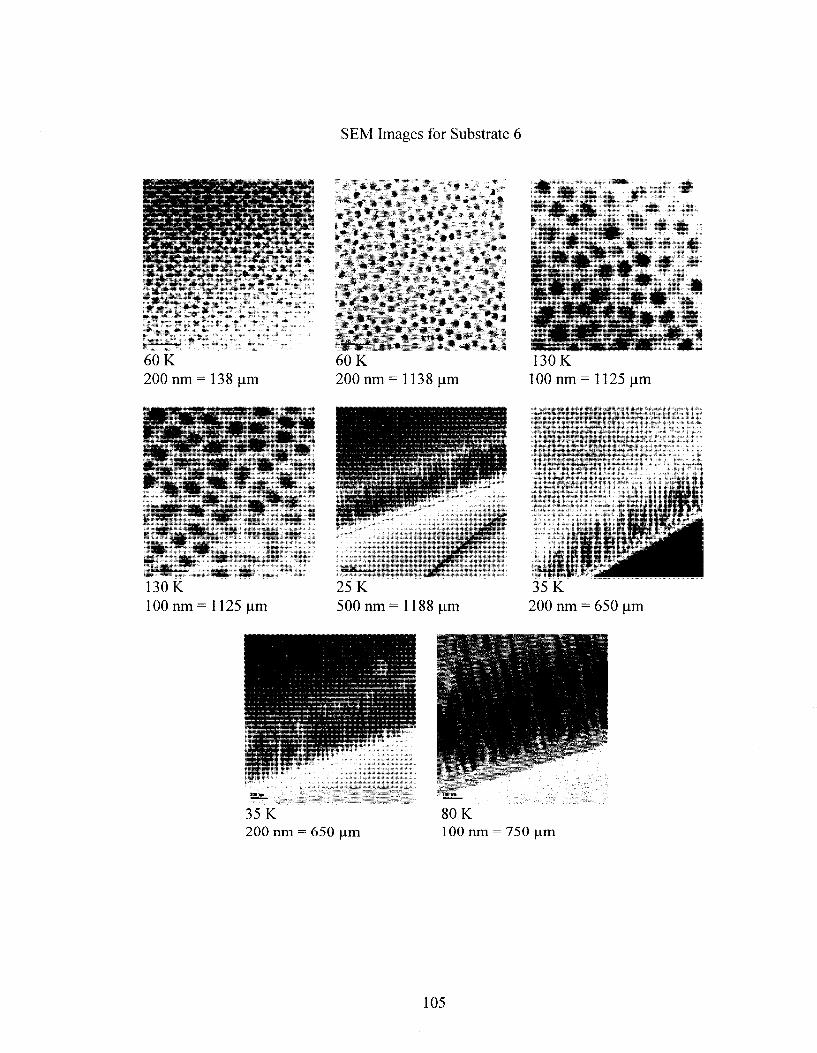
SEM Images for Substrate 6
60 K 200 nm
( # t , . f * * - * . ? #
138 \xm 60 K 200nm=1138|xm
5 # -.
130K 100 nm= 1125 urn
IV
* mm!*- r rj • * - * ! » • ™
• * « . * •
130 K 100nm=1125(im
25 K 500 nm = 1188 um
35 K 200 nm = 650 urn
35 K 200 nm = 650 \xm
80 K 100nm = 750 nm
105

Diameter Measurements for Substrate 6
Object type
Diameter
Diameter
Diameter
Diameter
Diameter
Diameter
Diameter
Diameter
Diameter
Diameter
Diameter
Diameter
Diameter
Diameter
Diameter
Diameter
Diameter
Diameter
Diameter
Diameter
Diameter
Diameter
Diameter
Diameter
Diameter
Diameter
Diameter
Diameter
Diameter
Diameter
Diameter
Diameter
Diameter
Diameter
Diameter
Diameter
Diameter
Diameter
Diameter
Diameter
Diameter
Result
205
171
185
236
218
188
165
191
242
189
279
201
190
199
212
221
198
206
204
182
192
209
224
185
226
226
181
261
211
219
218
202
214
225
258
202
235
232
216
207
211
Nanometers
36.03
30.05
32.51
41.48
38.31
33.04
29.00
33.57
42.53
33.22
49.03
35.33
33.39
34.97
37.26
38.84
34.80
36.20
35.85
31.99
33.74
36.73
39.37
32.51
39.72
39.72
31.81
45.87
37.08
38.49
38.31
35.50
37.61
39.54
45.34
35.50
41.30
40.77
37.96
36.38
37.08
Object type
Diameter
Diameter
Diameter
Diameter
Diameter
Diameter
Diameter
Diameter
Diameter
Diameter
Diameter
Diameter
Diameter
Diameter
Diameter
Diameter
Diameter
Diameter
Diameter
Diameter
Diameter
Diameter
Diameter
Diameter
Diameter
Diameter
Diameter
Diameter
Diameter
Diameter
Diameter
Diameter
Diameter
Diameter
Diameter
Diameter
Diameter
Diameter
Diameter
Diameter
Diameter
Result
196
194
231
266
267
194
250
222
210
222
236
211
236
257
243
237
237
234
231
195
198
236
229
173
236
228
207
171
246
208
227
263
235
180
191
254
260
259
213
156
188
Nanometers
34.45
34.09
40.60
46.75
46.92
34.09
43.94
39.02
36.91
39.02
41.48
37.08
41.48
45.17
42.71
41.65
41.65
41.12
40.60
34.27
34.80
41.48
40.25
30.40
41.48
40.07
36.38
30.05
43.23
36.56
39.89
46.22
41.30
31.63
33.57
44.64
45.69
45.52
37.43
27.42
33.04
Object type
Diameter
Diameter
Diameter
Diameter
Diameter
Diameter
Diameter
Diameter
Diameter
Diameter
Diameter
Diameter
Diameter
Diameter
Diameter
Diameter
Diameter
Diameter
Diameter
Diameter
Diameter
Diameter
Diameter
Diameter
Diameter
Diameter
Diameter
Diameter
Diameter
Diameter
Diameter
Diameter
Diameter
Diameter
Diameter
Diameter
Diameter
Diameter
Diameter
Diameter
Diameter
Result
243
248
243
247
253
227
216
215
263
263
222
211
160
260
212
222
257
213
304
225
255
242
256
276
241
231
236
283
193
259
244
235
233
269
252
221
286
233
264
251
240
Nanometers
42.71
43.59
42.71
43.41
44.46
39.89
37.96
37.79
46.22
46.22
39.02
37.08
28.12
45.69
37.26
39.02
45.17
37.43
53.43
39.54
44.82
42.53
44.99
48.51
42.36
40.60
41.48
49.74
33.92
45.52
42.88
41.30
40.95
47.28
44.29
38.84
50.26
40.95
46.40
44.11
42.18
106

Diameter Measurements for Substrate 6
Object type
Diameter
Diameter
Diameter
Diameter
Diameter
Diameter
Diameter
Diameter
Diameter
Diameter
Diameter
Diameter
Diameter
Diameter
Diameter
Diameter
Diameter
Diameter
Diameter
Diameter
Diameter
Diameter
Diameter
Diameter
Diameter
Diameter
Diameter
Diameter
Diameter
Diameter
Diameter
Diameter
Diameter
Diameter
Diameter
Diameter Diameter
Diameter
Diameter
Diameter
Diameter
Result
261
234
226
245
503
442
581
400
477
515
558
339
517
417
510
488
341
244
415
379
358
422
476
516
472
419
459
525
449
493
538
445
368
370
431
461 456
491
428
419
367
Manometers
45.87
41.12
39.72
43.06
44.71
39.29
51.64
35.56
42.40
45.78
49.60
30.13
45.96
37.07
45.33
43.38
30.31
21.69
36.89
33.69
31.82
37.51
42.31
45.87
41.96
37.24
40.80
46.67
39.91 43.82
47.82
39.56
32.71
32.89
38.31
40.98 40.53
43.64
38.04
37.24
32.62
Object type
Diameter
Diameter
Diameter
Diameter
Diameter
Diameter
Diameter
Diameter
Diameter
Diameter
Diameter
Diameter
Diameter
Diameter
Diameter
Diameter
Diameter
Diameter
Diameter
Diameter
Diameter
Diameter
Diameter
Diameter
Diameter
Diameter
Diameter
Diameter
Diameter
Diameter
Diameter
Diameter
Diameter
Diameter
Diameter
Diameter Diameter
Diameter
Diameter
Diameter
Diameter
Result
429
432
416
409
434
508
485
403
513
412
493
509
422
451
410
442
374
392
394
441
448
550
481
515
453
542
450
486
566
518
574
590
473
531
538
323 305
371
588
514
368
Manometers
38.13
38.40
36.98
36.36
38.58
45.16
43.11
35.82
45.60
36.62
43.82
45.24
37.51
40.09
36.44
39.29
33.24
34.84
35.02
39.20
39.82
48.89
42.76
45.78
40.27
48.18
40.00
43.20
50.31 46.04
51.02
52.44
42.04
47.20
47.82
28.71 27.11
32.98
52.27
45.69
32.71
Object type
Diameter
Diameter
Diameter
Diameter
Diameter
Diameter
Diameter
Diameter
Diameter
Diameter
Diameter
Diameter
Diameter
Diameter
Diameter
Diameter
Diameter
Diameter
Diameter
Diameter
Diameter
Diameter
Diameter
Diameter
Diameter
Diameter
Diameter
Diameter
Diameter
Diameter
Diameter
Diameter
Diameter
Diameter
Diameter
Diameter Diameter
Diameter
Diameter
Diameter
Diameter
Result
365
396
442
527
517
406
455
451
452
337
389
523
440
427
531
483
504
435
538
504
461
507
421
438
451
457
377
365
515
532
454
481
445
460
446
498 524
454
565
416
450
Nanometers
32.44
35.20
39.29
46.84
45.96
36.09
40.44
40.09
40.18
29.96
34.58
46.49
39.11
37.96
47.20
42.93
44.80
38.67
47.82
44.80
40.98
45.07
37.42
38.93
40.09
40.62
33.51
32.44
45.78
47.29
40.36
42.76
39.56
40.89
39.64
44.27 46.58
40.36
50.22
36.98
40.00
107

Nanopore Length Measurements for Substrate 6
Object type
Distance
Distance
Distance
Distance
Distance
Distance
Distance
Distance
Distance
Distance
Distance
Distance
Distance
Distance
Distance
Distance
Distance
Distance
Distance
Distance
Distance
Distance
Distance
Distance
Distance
Distance
Distance
Distance
Distance
Distance
Distance
Distance
Distance
Distance
Distance
Distance Distance
Distance
Distance
Distance
Distance
Result
1300
1206
1179
1136
1151
1176
1149 1201
1200
1277
1225
1219
1190
1086
1141
1149
1115
1081
1090
1185
1102
1153
1264
1268
1208
1250
1301
1076
1203
1179
1213
1211
1194
1062
1275
1279 1243
1229
1703
2000
1943
Nanometers
547.14
507.58
496.21
478.11
484.43
494.95
483.59 505.47
505.05
537.46
515.57
513.05
500.84
457.07
480.22
483.59
469.28
454.97
458.75
498.74
463.80
485.27
531.99
533.67
508.42
526.09
547.56
452.86
506.31
496.21
510.52
509.68
502.53
446.97
536.62
538.30 523.15
517.26
716.75
615.38
597.85
Object type
Distance
Distance
Distance
Distance
Distance
Distance
Distance Distance
Distance
Distance
Distance
Distance
Distance
Distance
Distance
Distance
Distance
Distance
Distance
Distance
Distance
Distance
Distance
Distance
Distance
Distance
Distance
Distance
Distance
Distance
Distance
Distance
Distance
Distance
Distance
Distance Distance
Distance
Distance
Distance
Distance
Result
1942
1851
1838
1788
1802
1737
1915
1838
1815
1841
1702
1758
3412
1909
1843
1714
1614
1614
1589
1739
1739
1764
1634
2170
1656
1671
2191
2088
2083
2022
2243
2284
2246
2164
1942
1829 2004
2239
1855
2035
2227
Nanometers
597.54
569.54
565.54
550.15
554.46
534.46
589.23 565.54
558.46
566.46
523.69
540.92
1049.85
587.38
567.08
527.38
496.62
496.62
488.92
535.08
535.08
542.77
502.77
667.69
509.54
514.15
674.15
642.46
640.92
622.15
690.15
702.77
691.08
665.85
597.54
562.77 616.62
688.92
570.77
626.15
685.23
Object type
Distance
Distance
Distance
Distance
Distance
Distance
Distance
Distance
Distance
Distance
Distance
Distance
Distance
Distance
Distance
Distance
Distance
Distance
Distance
Distance
Distance
Distance
Distance
Distance
Distance
Result
2202
2123
2038
2075
1901
1892
2101
2230
2232
2189
2193
3856
3919
3891
3920
3989
3820
3929
3781
3770
3836
3775
3697
2216
1763
Nanometers
677.54
653.23
627.08
638.46
584.92
£82.15
646.46
686.15
686.77
673.54
674.77
514.13
522.53
518.80
522.67
531.87
509.33
523.87
504.13
502.67
511.47
503.33
492.93
681.85
542.46
108

Appendix H. Substrate 7 Data
109

SEM Images for Substrate 7
200 ran = 938 um
JMb JJk flHI -,«te
100 K 100 nm 938 um
'••.• Jit** •<*.'; 60 K 200 nm= 1138 um
850 um
35 K 200 nm = 650 um
* i |p ^^ ^^ ^B tfk
100 K 100nm = 928 um
25 K 500 nm= 1188 um
« " i * * ; - > i
45 K 200 nm 850 [im
110

Diameter Measurements for Substrate 7
Object type
Diameter
Diameter
Diameter
Diameter
Diameter
Diameter
Diameter
Diameter
Diameter
Diameter
Diameter
Diameter
Diameter
Diameter
Diameter
Diameter
Diameter
Diameter
Diameter
Diameter
Diameter
Diameter
Diameter
Diameter
Diameter
Diameter
Diameter
Diameter
Diameter
Diameter
Diameter
Diameter
Diameter
Diameter
Diameter
Diameter Diameter
Diameter
Diameter
Diameter
Diameter
Result
274
277
248
298
316
287
319
326
285
365
364
343
326
308
356
279
308
293
310
319
326
329
350
377
314
330
310
305
299
353
332
296
315
317
304
330 331
315
317
277
303
Nanometers
58.42
59.06
52.88
63.54
67.38
61.19
68.02
69.51
60.77
77.83
77.61
73.13
69.51
65.67
75.91
59.49
65.67
62.47
66.10
68.02
69.51
70.15
74.63
80.38
66.95
70.36
66.10
65.03
63.75
75.27
70.79
63.11
67.16
67.59
64.82
70.36 70.58
67.16
67.59
59.06
64.61
Object type
Diameter
Diameter
Diameter
Diameter
Diameter
Diameter
Diameter
Diameter
Diameter
Diameter
Diameter
Diameter
Diameter
Diameter
Diameter
Diameter
Diameter
Diameter
Diameter
Diameter
Diameter
Diameter
Diameter
Diameter
Diameter
Diameter
Diameter
Diameter
Diameter
Diameter
Diameter
Diameter
Diameter
Diameter
Diameter
Diameter Diameter
Diameter
Diameter
Diameter
Diameter
Result
295
303
311
355
352
282
332
328
320
325
350
301
347
347
307
353
313
330
338
353
352
355
342
410
416
354
363
407
442
409
390
308
342
367
392
310 354
420
450 457
352
Nanometers
62.90
64.61
66.31
75.69
75.05
60.13
70.79
69.94
68.23
69.30
74.63
64.18
73.99
73.99
65.46
75.27
66.74
70.36
72.07
75.27
75.05
75.69
72.92
72.06
73.11
62.21
63.80
71.53
77.68
71.88
68.54
54.13
60.11
64.50
68.89
54.48 62.21
73.81
79.09 80.32
61.86
Object type
Diameter
Diameter
Diameter
Diameter
Diameter
Diameter
Diameter
Diameter
Diameter
Diameter
Diameter
Diameter
Diameter
Diameter
Diameter
Diameter
Diameter Diameter
Diameter
Diameter
Diameter
Diameter
Diameter
Diameter
Diameter
Diameter
Diameter
Diameter
Diameter
Diameter
Diameter
Diameter
Diameter
Diameter
Diameter
Diameter Diameter
Diameter
Diameter
Diameter
Diameter
Result
345
363
387
289
366
383
320
360
418
393
412
301
406
388
423
266
329
348
356
430
387
380
380
379
342
384
412
382
395
429
405
367
384
299
368
443 421
427
337
421
342
Nanometers
60.63
63.80
68.01
50.79
64.32
67.31
56.24
63.27
73.46
69.07
72.41
52.90
71.35
68.19
74.34
46.75
57.82
61.16
62.57
75.57
68.01
66.78
66.78
66.61
60.11
67.49
72.41
67.14
69.42
75.40
71.18
64.50
67.49
52.55
64.67
77.86 73.99
75.04
59.23
73.99
60.11
111

Diameter Measurements for Substrate 7
Object type
Diameter
Diameter
Diameter
Diameter
Diameter
Diameter
Diameter
Diameter
Diameter
Diameter
Diameter
Diameter
Diameter
Diameter
Diameter
Diameter
Diameter
Diameter
Diameter
Diameter
Diameter
Diameter
Diameter
Diameter
Diameter
Diameter
Diameter
Diameter
Diameter
Diameter
Diameter
Diameter
Diameter
Diameter
Diameter
Diameter
Diameter
Diameter
Diameter
Diameter
Diameter
Result
345
435
392
400
600
569
630
517
634
819
733
667
647
596
623
530
493
474
752
645
633
662
691
613
702
596
638
623
571
582
545
560
643
503
515
543
602
453
546
643
637
Nanometers
60.63
76.45
68.89
70.30
63.97
60.66
67.16
55.12
67.59
87.31
78.14
71.11
68.98
63.54
66.42
56.50
52.56
50.53
80.17
68.76
67.48
70.58
73.67
65.35
74.84
63.54
68.02
66.42
60.87
62.05
58.10
59.70
68.55
53.62
54.90
57.89
64.18
48.29
58.21
68.55
67.91
Object type
Diameter
Diameter
Diameter
Diameter
Diameter
Diameter
Diameter
Diameter
Diameter
Diameter
Diameter
Diameter
Diameter
Diameter
Diameter
Diameter
Diameter
Diameter
Diameter
Diameter
Diameter
Diameter
Diameter
Diameter
Diameter
Diameter
Diameter
Diameter
Diameter
Diameter
Diameter
Diameter
Diameter
Diameter
Diameter
Diameter
Diameter
Diameter
Diameter
Diameter
Diameter
Result
611
535
528
632
551
520
726
658
538
594
591
573
680
719
650
598
498
661
590
583
652
703
624
641
651
542
557
550
610
611
549
613
473
552
661
465
431
499
547
595
508
Nanometers
65.14
57.04
56.29
67.38
58.74
55.44
77.40
70.15
57.36
63.33
63.01
61.09
72.49
76.65
69.30
63.75
53.09
70.47
62.90
62.15
69.51
74.95
66.52
68.34
69.40
57.78
59.38
58.64
65.03
65.14
58.53
65.35
50.43
58.85
70.47
49.57
45.95
53.20
58.32
63.43
54.16
Object type
Diameter
Diameter
Diameter
Diameter
Diameter
Diameter
Diameter
Diameter
Diameter
Diameter
Diameter
Diameter
Diameter
Diameter
Diameter
Result
594
432
565
560
428
633
591
614
577
508
661
705
672
632
516
Nanometers
63.33
46.06
60.23
59.70
45.63
67.48
63.01
65.46
61.51
54.16
70.47
75.16
71.64
67.38
55.01
112

Nanopore Length Measurements for Substrate 7
Object type
Distance
Distance
Distance
Distance
Distance
Distance
Distance
Distance
Distance
Distance
Distance
Distance
Distance
Distance
Distance
Distance
Distance
Distance
Distance
Distance
Distance
Distance
Distance
Distance
Distance
Distance
Distance
Distance
Distance
Distance
Distance
Distance
Distance
Distance
Distance
Distance Distance
Distance
Distance
Distance
Distance
Result
1451
1413
1439
1406
1338
1414
1428
1419
1440
1496
1500
1424
1500
1501
1404
1413
1453
1516
1464
1458
1430
1353
1318
1361
1355
1251
1338
1329
1313
1376
1401
1388
1401
1325
1313
1268
1292
1347
1244
1298
1256
Nanometers
853.53
831.18
846.47
827.06
787.06
831.76
840.00
834.71
847.06
880.00
882.35
837.65
882.35
882.94
825.88
831.18
854.71
891.76
861.18
857.65
841.18
795.88
775.29
800.59
797.06
735.88
787.06
781.76
772.35
809.41
824.12
816.47
824.12
779.41
772.35
745.88 760.00
792.35
872.98
910.88
881.40
Object type
Distance
Distance
Distance
Distance
Distance
Distance
Distance
Distance
Distance
Distance
Distance
Distance
Distance
Distance
Distance
Distance
Distance
Distance
Distance
Distance
Distance
Distance
Distance
Distance
Distance
Distance
Distance
Distance
Distance
Distance
Distance
Distance
Distance
Distance
Distance
Distance Distance
Distance
Distance
Distance
Distance
Result
1231
1250
1227
1231
1197
1217
1201
1225
1115
1265
1240
1233
1171
1157
1144
1178
1209
1162
1193
1134
1143
1204
1280
1194
1230
1202
1226
1290
1165
1223
1214
1113
1103
1121
1183
1174
1199
1248
1233
3202
3004
Nanometers
863.86
877.19
861.05
863.86
840.00
854.04
842.81
859.65
782.46
887.72
870.18
865.26
821.75
811.93
802.81
826.67
848.42
815.44
837.19
795.79
802.11
844.91
898.25
837.89
863.16
843.51
860.35
905.26
817.54
858.25
851.93
781.05
774.04
786.67
830.18
823.86 841.40
875.79
865.26
985.23
924.31
Object type
Distance
Distance
Distance
Distance
Distance
Distance
Distance
Distance
Distance
Distance
Distance
Distance
Distance
Distance
Distance
Distance
Distance
Distance
Distance
Distance
Distance
Distance
Distance
Distance
Distance
Distance
Distance
Distance
Distance
Distance
Distance
Distance
Distance
Distance
Distance
Distance
Distance
Result
2896
2984
2966
2859
2801
2805
2812
3057
3006
3030
3185
2888
2916
2871
2737
2816
2694
2850
2796
2686
3616
3896
3895
3700
3597
3552
3580
3656
3393
3464
3221
3356
3566
3545
3355
2921
1197
Nanometers
891.08
918.15
912.62
879.69
861.85
863.08
865.23
940.62
924.92
932.31
980.00
888.62
897.23
883.38
842.15
866.46
828.92
876.92
860.31
826.46
850.82
916.71
916.47
870.59
846.35
835.76
842.35
860.24
798.35
815.06
757.88
789.65
839.06
834.12
789.41
898.77
840.00
113

Appendix I. Substrate 8 Data
114

SEM Images for Substrate 8
50 K 200 nm = 938 um
50 K 200 nm = 938 um
80 K 100 nm = 750 urn
WMi} IP
..} ' i . -
.«
100 K 100nm = 938(im
15K 1 |am= 1425 (am
35 K 200 nm = 650 nm
50 K 200 nm = 938 ^m
18K 0.5 |nm = 850 jam
115

Diameter Measurements for Substrate 8
Object type
Diameter
Diameter
Diameter
Diameter
Diameter
Diameter
Diameter
Diameter
Diameter
Diameter
Diameter
Diameter
Diameter
Diameter
Diameter
Diameter
Diameter
Diameter
Diameter
Diameter
Diameter
Diameter
Diameter
Diameter
Diameter
Diameter
Diameter
Diameter
Diameter
Diameter
Diameter
Diameter
Diameter
Diameter
Diameter
Diameter Diameter
Diameter
Diameter
Diameter
Diameter
Result
239
226
261
238
240
259
259
227
238
236
227
196
248
179
245
222
240
230
229
225
260
234
230
217
237
259
208
219
237
237
217
217
268
247
221
217 240
261
242
208
227
Manometers
50.96
48.19
55.65
50.75
51.17
55.22
55.22
48.40
50.75
50.32
48.40
41.79
52.88
38.17
52.24
47.33
51.17
49.04
48.83
47.97
55.44
49.89
49.04
46.27
50.53
55.22
44.35
46.70
50.53
50.53
46.27
46.27
57.14
52.67
47.12
46.27 51.17
55.65
51.60
44.35
48.40
Object type
Diameter
Diameter
Diameter
Diameter
Diameter
Diameter
Diameter
Diameter
Diameter
Diameter
Diameter
Diameter
Diameter
Diameter
Diameter
Diameter
Diameter
Diameter
Diameter
Diameter
Diameter
Diameter
Diameter
Diameter
Diameter
Diameter
Diameter
Diameter
Diameter
Diameter
Diameter
Diameter
Diameter
Diameter
Diameter
Diameter Diameter
Diameter
Diameter
Diameter
Diameter
Result
225
250
169
232
233
244
220
237
234
205
237
239
260
268
237
226
238
238
233
261
224
259
296
230
248
233
254
259
268
213
281
255
212
277
244
229 226
200
213
252
244
Nanometers
47.97
53.30
36.03
49.47
49.68
52.03
46.91
50.53
49.89
43.71
50.53
50.96
55.44
57.14
50.53
48.19
50.75
50.75
49.68
55.65
47.76
55.22
63.11
49.04
52.88
49.68
54.16
55.22
57.14
45.42
59.91 54.37
45.20
59.06
52.03
48.83 48.19
42.64
45.42
53.73
52.03
Object type
Diameter
Diameter
Diameter
Diameter
Diameter
Diameter
Diameter
Diameter
Diameter
Diameter
Diameter
Diameter
Diameter
Diameter
Diameter
Diameter
Diameter
Diameter
Diameter
Diameter
Diameter
Diameter
Diameter
Diameter
Diameter
Diameter
Diameter
Diameter
Diameter
Diameter
Diameter
Diameter
Diameter
Diameter
Diameter
Diameter Diameter
Diameter
Diameter
Diameter
Diameter
Result
229
237
346
273
262
262
269
271
244
321
227
230
266
257
254
272
265
243
273
217
293
265
266
260
295
269
293
239
257
293
246 292
271
283
224 264 244
258
252
283
238
Nanometers
48.83
50.53
73.77
58.21
55.86
55.86
57.36
57.78
52.03
68.44
48.40
49.04
56.72
54.80
54.16
58.00
56.50
51.81
58.21
46.27
62.47
56.50
56.72
55.44
62.90
57.36
62.47
50.96
54.80
62.47
52.45
62.26
57.78
60.34
47.76
56.29 52.03
55.01
53.73
60.34
50.75
116

Diameter Measurements for Substrate 8
Object type
Diameter
Diameter
Diameter
Diameter
Diameter
Diameter
Diameter
Diameter
Diameter
Diameter
Diameter
Diameter
Diameter
Diameter
Diameter
Diameter
Diameter
Diameter
Diameter
Diameter
Diameter
Diameter
Diameter
Diameter
Diameter
Diameter
Diameter
Diameter
Diameter
Diameter
Diameter
Diameter
Diameter
Diameter
Diameter
Diameter
Diameter
Diameter
Diameter
Diameter
Diameter
Result
268
239
262
291
302
326
257
331
352
274
266
356
359
377
338
312
432
278
343
296
372
273
313
266
317
413
312
375
365
332
290
458
338
382
262
304
320
433
313
213
364
Nanometers
57.14
50.96
55.86
62.05
40.27
43.47
34.27
44.13
46.93
36.53
35.47
47.47
47.87
50.27
45.07
41.60
57.60
37.07
45.73
39.47
49.60
36.40
41.73
35.47
42.27
55.07
41.60
50.00
48.67
44.27
38.67
61.07
45.07
50.93
34.93
40.53
42.67
57.73
41.73
28.40
48.53
Object type
Diameter
Diameter
Diameter
Diameter
Diameter
Diameter
Diameter
Diameter
Diameter
Diameter
Diameter
Diameter
Diameter
Diameter
Diameter
Diameter
Diameter
Diameter
Diameter
Diameter
Diameter
Diameter
Diameter
Diameter
Diameter
Diameter
Diameter
Diameter
Diameter
Diameter
Diameter
Diameter
Diameter
Diameter
Diameter
Diameter
Diameter
Diameter
Diameter
Diameter
Diameter
Result
361
391
332
397
291
380
349
395
407
280
435
316
400
396
366
432
389
359
415
398
353
378
386
362
338
346
268
473
398
477
491
456
351
438
422
390
383
428
407
357
380
Nanometers
48.13
52.13
44.27
52.93
38.80
50.67
46.53
52.67
54.27
37.33
58.00
42.13
53.33
52.80
48.80
57.60
51.87
47.87
55.33
53.07
47.07
50.40
51.47
48.27
45.07
46.13
35.73
50.43
42.43
50.85
52.35
48.61
37.42
46.70
44.99
41.58
40.83
45.63
43.39
38.06
40.51
Object type
Diameter
Diameter
Diameter
Diameter
Diameter
Diameter
Diameter
Diameter
Diameter
Diameter
Diameter
Diameter
Diameter
Diameter
Diameter
Diameter
Diameter
Diameter
Diameter
Diameter
Diameter
Diameter
Diameter
Diameter
Diameter
Diameter
Diameter
Diameter
Diameter
Diameter
Diameter
Diameter
Diameter
Diameter
Diameter
Diameter
Diameter
Diameter
Diameter
Diameter
Diameter
Result
488
357
525
410
418
427
474
519
419
594
317
428
436
438
456
499
390
365
336
494
469
495
420
490
452
511
526
481
477
427
444
505
475
407
335
421
439
400
500
536
421
Nanometers
52.03
38.06
55.97
43.71
44.56
45.52
50.53
55.33
44.67
63.33
33.80
45.63
46.48
46.70
48.61
53.20
41.58
38.91
35.82
52.67
50.00
52.77
44.78
52.24
48.19
54.48
56.08
51.28
50.85
45.52
47.33
53.84
50.64
43.39
35.71
44.88
46.80
42.64
53.30
57.14
44.88
117

Nanopore Length Measurements for Substrate 8
Object type
Distance
Distance
Distance
Distance
Distance
Distance
Distance
Distance
Distance
Distance
Distance
Distance
Distance
Distance
Distance
Distance
Distance
Distance
Distance
Distance
Distance
Distance
Distance
Distance
Distance
Distance
Distance
Distance
Distance
Distance
Distance
Distance
Distance
Distance
Distance
Distance
Distance
Distance
Distance
Distance
Distance
Result
1027
1039
1001
1061
1121
938
925
1005
1007
1069
1115
1004
1065
1098
1033
1019
1013
1026
1055
1527
977
974
1009
889
979
962
1014
985
1111
1067
2558
2516
2484
2593
2547
2676
2693
2580
2645
2643
2567
Nanometers
720.70
729.12
702.46
744.56
786.67
658.25
649.12
705.26
706.67
750.18
782.46
704.56
747.37
770.53
724.91
715.09
710.88
720.00
740.35
1071.58
685.61
683.51
708.07
623.86
687.02
675.09
711.58
691.23
779.65
748.77
787.08
774.15
764.31
797.85
783.69
823.38
828.62
793.85
813.85
813.23
789.85
Object type
Distance
Distance
Distance
Distance
Distance
Distance
Distance
Distance
Distance
Distance
Distance
Distance
Distance
Distance
Distance
Distance
Distance
Distance
Distance
Distance
Distance
Distance
Distance
Distance
Distance
Distance
Distance
Distance
Distance
Distance
Distance
Distance
Distance
Distance
Distance
Distance
Distance
Distance
Distance
Distance
Distance
Result
2228
2214
2300
2342
2359
2358
2265
2406
2164
2218
2234
3664
3944
3689
3632
4307
3088
4908
3513
3281
3355
3458
3305
3378
3399
3195
3307
3456
3626
4695
919
807
834
864
827
859
767
752
710
827
871
Nanometers
685.54
681.23
707.69
720.62
725.85
725.54
696.92
740.31
665.85
682.46
687.38
781.24
840.94
786.57
774.41
918.34
658.42
1046.48
749.04
699.57
715.35
737.31
704.69
720.26
724.73
681.24
705.12
736.89
773.13
1001.07
644.91
566.32
585.26
606.32
580.35
602.81
538.25
527.72
498.25
580.35
611.23
Object type
Distance
Distance
Distance
Distance
Distance
Distance
Distance
Distance
Distance
Distance
Distance
Distance
Distance
Distance
Distance
Distance
Distance
Distance
Distance
Distance
Distance
Distance
Distance
Distance
Distance
Distance
Distance
Distance
Distance
Result
821
862
924
944
845
844
878
868
724
850
803
816
844
783
800
762
772
885
942
934
892
879
919
845
1117
817
770
852
2208
Nanometers
576.14
604.91
648.42
662.46
592.98
592.28
616.14
609.12
508.07
596.49
563.51
572.63
592.28
549.47
561.40
534.74
541.75
621.05
661.05
655.44
625.96
616.84
644.91
592.98
783.86
573.33
540.35
597.89
679.38
118

Appendix J. Center Point 1 Substrate Data
119

SEM Images for Center Point 1 Substrate
50 K 200 nm = 938 urn
50 K 200 nm 938 urn
20 K 500 nm = 938 um
20 K 500 nm = 938 im
30 K 500 nm= 1425 jun
120

Diameter Measurements for Center Point Run 1
Object type
Diameter
Diameter
Diameter
Diameter
Diameter
Diameter
Diameter
Diameter
Diameter
Diameter
Diameter
Diameter
Diameter
Diameter
Diameter
Diameter
Diameter
Diameter
Diameter
Diameter
Diameter
Diameter
Diameter
Diameter
Diameter
Diameter
Diameter
Diameter
Diameter
Diameter
Diameter
Diameter
Diameter
Diameter
Diameter
Diameter
Diameter
Diameter
Diameter
Diameter
Diameter
Result
344
322
316
294
345
337
354
305
334
275
243
279
306
287
298
397
309
273
318
302
266
321
298
327
294
302
267
360
333
321
319
304
375
300
335
325
359
282
355
345
354
Nanometers
73.35
58.66
57.38
62.69
73.56
71.86
75.48
65.03
71.22
58.64
51.81
59.49
65.25
61.19
63.54
84.65
65.88
58.21
67.80
64.39
56.72
68.44
63.54
69.72
62.69
64.39
56.93
76.76
71.00
68.44
68.02
64.82
79.96
63.97
71.43
69.30
76.55
60.13
75.69
73.56
75.48
Object type
Diameter
Diameter
Diameter
Diameter
Diameter
Diameter
Diameter
Diameter
Diameter
Diameter
Diameter
Diameter
Diameter
Diameter
Diameter
Diameter
Diameter
Diameter
Diameter
Diameter
Diameter
Diameter
Diameter
Diameter
Diameter
Diameter
Diameter
Diameter
Diameter
Diameter
Diameter
Diameter
Diameter
Diameter
Diameter
Diameter
Diameter
Diameter
Diameter
Diameter
Diameter
Result
303
279
350
270
388
304
304
306
285
309
318
337
318
310
339
275
277
306
294
255
254
319
286
337
308
303
265
301
298
318
347
207
295
384
279
271
288
406
249
303
Nanometers
64.61
59.49
74.63
57.57
82.73
64.82
64.82
65.25
60.77
65.88
67.80
71.86
67.80
66.10
72.28
58.64
59.06
65.25
62.69
54.37
54.16
68.02
60.98
71.86
65.67
64.61
56.50
64.18
63.54
67.80
73.99
44.14
62.90
81.88
59.49
57.78
61.41
86.57
53.09
64.61
274 J58.42
Object type
Diameter
Diameter
Diameter
Diameter
Diameter
Diameter
Diameter
Diameter
Diameter
Diameter
Diameter
Diameter
Diameter
Diameter
Diameter
Diameter
Diameter
Diameter
Diameter
Diameter
Diameter
Diameter
Diameter
Diameter
Diameter
Diameter
Diameter
Diameter
Diameter
Diameter
Diameter
Diameter
Diameter
Diameter
Diameter
Diameter
Diameter
Diameter
Diameter
Diameter
Diameter
Result
241
384
303
282
304
323
385
342
251
329
323
333
282
266
332
261
337
334
277
298
350
297
338
310
305
383
304
253
238
338
302
302
300
305
337
285
364
288
317
325
293
Nanometers
51.39
81.88
64.61
60.13
64.82
68.87
82.09
72.92
53.52
70.15
68.87
71.00
60.13
56.72
70.79
55.65
71.86
71.22
59.06
63.54
74.63
63.33
72.07
66.10
65.03
81.66
64.82
53.94
50.75
72.07
64.39
64.39
63.97
65.03
71.86
60.77
77.61
61.41
67.59
69.30
62.47
121

Nanopore Length Measurements for Center Point Run 1
Object type
Distance
Distance
Distance
Distance
Distance
Distance
Distance
Distance
Distance
Distance
Distance
Distance
Distance
Distance
Distance
Distance
Distance
Distance
Distance
Distance
Distance
Distance
Distance
Distance
Distance
Distance
Distance
Distance
Distance
Distance
Distance
Distance
Distance
Distance
Distance
Distance Distance
Distance
Distance
Distance
Result
1380
1451
1199
1180
1257
1413
1354
1312
1315
1340
1488
1505
1538
1438
1544
1526
1379
1447
1463
1381
1412
1387
1500
1438
1450
1401
1463
1438
1413
1433
1399
1326
1250
1200
1291
1189 1411
1425
1306
1391
Nanometers
735.61
773.45
639.13
629.00
670.04
753.20
721.75
699.36
700.96
714.29
793.18
802.24
819.83
766.52
823.03
813.43
735.07
771.32
779.85
736.14
752.67
739.34
799.57
766.52
772.92
746.80
779.85
766.52
753.20
763.86
745.74
706.82
666.31
639.66
688.17
633.80 752.13
759.59
696.16
741.47
Object type
Distance
Distance
Distance
Distance
Distance
Distance
Distance
Distance
Distance
Distance
Distance
Distance
Distance
Distance
Distance
Distance
Distance
Distance
Distance
Distance
Distance
Result
1237
1241
1222
1328
1402
2352
2148
2366
2182
2204
2190
2151
2128
2202
2190
1923
2355
2176
2315
2359
1322
Nanometers
659.38
661.51
651.39
707.89
747.33
825.26
753.68
830.18
765.61
773.33
768.42
754.74
746.67
772.63
768.42
674.74
826.32
763.51
812.28
827.72
704.69
122

Appendix K. Center Point Repeatability Substrate Data
123

SEM Images for Center Point Repeatability Substrate
18K 0.5 |ira = 850 um
35 K 200 nm = 650 um
20 K 500 nm = 938 urn
50 K 200 nm = 938 um
15K 1 (am = 1425 um
18K 0.5 um = 850 um
20 K 500nm = 938 im
11 K 2 um = 1038 |^m
124
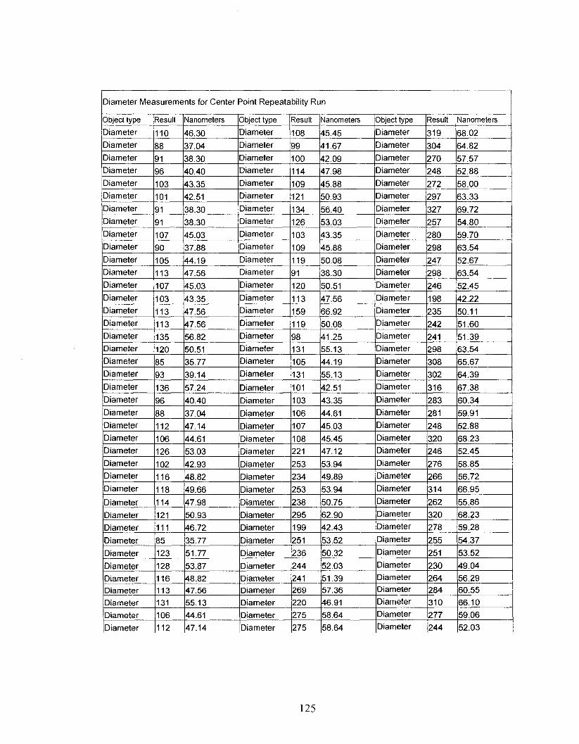
Diameter Measurements for Center Point Repeatability Run
Object type
Diameter
Diameter
Diameter
Diameter
Diameter
Diameter
Diameter
Diameter
Diameter
Diameter
Diameter
Diameter
Diameter
Diameter
Diameter
Diameter
Diameter
Diameter
Diameter
Diameter
Diameter
Diameter
Diameter
Diameter
Diameter
Diameter
Diameter
Diameter
Diameter
Diameter
Diameter
Diameter
Diameter
Diameter
Diameter
Diameter
Diameter
Diameter
Diameter
Diameter
Result
110
88
91
96
103
101
91
91
107
90
105
113
107
103
113
113
135
120
85
93
136
96
88
112
106
126
102
116
118
114
121
111
85
123
128
116
113
131
106
112
Nanometers
46.30
37.04
38.30
40.40
43.35
42.51
38.30
38.30
45.03
37.88
44.19
47.56
45.03
43.35
47.56
47.56
56.82
50.51
35.77
39.14
57.24
40.40
37.04
47.14
44.61
53.03
42.93
48.82
49.66
47.98
50.93
46.72
35.77
51.77
53.87
48.82
47.56
55.13
44.61
47.14
Object type
Diameter
Diameter
Diameter
Diameter
Diameter
Diameter
Diameter
Diameter
Diameter
Diameter
Diameter
Diameter
Diameter
Diameter
Diameter
Diameter
Diameter
Diameter
Diameter
Diameter
Diameter
Diameter
Diameter
Diameter
Diameter
Diameter
Diameter
Diameter
Diameter
Diameter
Diameter
Diameter
Diameter
Diameter
Diameter
Diameter
Diameter
Diameter
Diameter
Diameter
Result
108
99
100
114
109
121
134
126
103
109
119
91
120
113
159
119
98
131
105
131
101
103
106
107
108
221
253
234
253
238
295
199
251
236
244
241
269
220
275
275
Nanometers
45.45
41.67
42.09
47.98
45.88
50.93
56.40
53.03
43.35
45.88
50.08
38.30
50.51
47.56
66.92
50.08
41.25
55.13
44.19
55.13
42.51
43.35
44.61
45.03
45.45
47.12
53.94
49.89
53.94
50.75
62.90
42.43
53.52
50.32
52.03
51.39
57.36
46.91
58.64
58.64
Object type
Diameter
Diameter
Diameter
Diameter
Diameter
Diameter
Diameter
Diameter
Diameter
Diameter
Diameter
Diameter
Diameter
Diameter
Diameter
Diameter
Diameter
Diameter
Diameter
Diameter
Diameter
Diameter
Diameter
Diameter
Diameter
Diameter
Diameter
Diameter
Diameter
Diameter
Diameter
Diameter
Diameter
Diameter
Diameter
Diameter
Diameter
Diameter
Diameter
Diameter
Result
319
304
270
248
272
297
327
257
280
298
247
298
246
198
235
242
241
298
308
302
316
283
281
248
320
246
276
266
314
262
320
278
255
251
230
264
284
310
277
244
Nanometers
68.02
64.82
57.57
52.88
58.00
63.33
69.72
54.80
59.70
63.54
52.67
63.54
52.45
42.22
50.11
51.60
51.39
63.54
65.67
64.39
67.38
60.34
59.91
52.88
68.23
52.45
58.85
56.72
66.95
55.86
68.23
59.28
54.37
53.52
49.04
56.29
60.55
66.10
59.06
52.03
125

Diameter Measurements for Center Point Repeatability Run
Object type
Diameter
Diameter
Diameter
Diameter
Diameter
Diameter
Diameter
Diameter
Diameter
Diameter
Diameter
Diameter
Diameter
Diameter
Diameter
Diameter
Diameter
Diameter
Diameter
Diameter
Diameter
Diameter
Diameter
Diameter
Diameter
Diameter
Diameter
Diameter
Diameter
Diameter
Diameter
Diameter
Diameter
Diameter
Diameter
Diameter
Diameter
Diameter
Diameter
Diameter
Result
308
265
284
335
293
286
336
331
358
253
110
88
91
96
103
101
91
91
107
90
105
113
107
103
113
113
135
120
85
93
136
96
88
112
106
126
102
116
118
114
Nanometers
65.67
56.50
60.55
71.43
62.47
60.98
71.64
70.58
76.33
53.94
58.64
46.91
48.51
51.17
54.90
53.84
48.51
48.51
57.04
47.97
55.97
60.23
57.04
54.90
60.23
60.23
71.96
63.97
45.31
49.57
72.49
51.17
46.91
59.70
56.50
67.16
54.37
61.83
62.90
60.77
Object type
Diameter
Diameter
Diameter
Diameter
Diameter
Diameter
Diameter
Diameter
Diameter
Diameter
Diameter
Diameter
Diameter
Diameter
Diameter
Diameter
Diameter
Diameter
Diameter
Diameter
Diameter
Diameter
Diameter
Diameter
Diameter
Diameter
Diameter
Diameter
Diameter
Diameter
Diameter
Diameter
Diameter
Diameter
Diameter
Diameter
Diameter
Diameter
Diameter
Diameter
Result
121
111
85
123
128
116
113
131
106
112
108
99
100
114
109
121
134
126
103
109
119
91
120
113
159
119
98
131
105
131
101
103
106
107
108
194
153
202
197
195
Nanometers
64.50
59.17
45.31
65.57
68.23
61.83
60.23
69.83
56.50
59.70
57.57
52.77
53.30
60.77
58.10
64.50
71.43
67.16
54.90
58.10
63.43
48.51
63.97
60.23
84.75
63.43
52.24
69.83
55.97
69.83
53.84
54.90
56.50
57.04
57.57
41.36
32.62
43.07
42.00
41.58
Object type
Diameter
Diameter
Diameter
Diameter
Diameter
Diameter
Diameter
Diameter
Diameter
Diameter
Diameter
Diameter
Diameter
Diameter
Diameter
Diameter
Diameter
Diameter
Diameter
Diameter
Diameter
Diameter
Diameter
Diameter
Diameter
Diameter
Diameter
Diameter
Diameter
Diameter
Diameter
Diameter
Diameter
Diameter
Diameter
Diameter
Diameter
Diameter
Diameter
Diameter
Result
233
241
193
199
177
188
221
189
230
216
199
244
214
197
186
227
194
217
219
195
241
204
202
197
224
190
247
262
227
264
275
288
258
216
273
269
250
222
244
257
Nanometers
49.68
51.39
41.15
42.43
37.74
40.09
47.12
40.30
49.04
46.06
42.43
52.03
45.63
42.00
39.66
48.40
41.36
46.27
46.70
41.58
51.39
43.50
43.07
42.00
47.76
40.51
52.67
55.86
48.40
56.29
58.64
61.41
55.01
46.06
58.21
57.36
53.30
47.33
52.03
54.80
126

Nanopore Length Measurements for Center Point Repeatability Run
Object type
Distance
Distance
Distance
Distance
Distance
Distance
Distance
Distance
Distance
Distance
Distance
Distance
Distance
Distance
Distance
Distance
Distance
Distance
Distance
Distance
Distance
Distance
Distance
Distance
Distance
Distance
Distance
Distance
Distance
Distance
Distance
Distance
Distance
Distance
Distance
Distance Distance
Distance
Distance
Distance
Result
488
439
532
476
475
488
465
478
453
483
465
444
504
521
422
427
405
431
475
549
588
541
608
559
643
500
528
694
661
606
658
639
508
490
576
628 612
516
529
463
Nanometers
650.67
585.33
709.33
634.67
633.33
650.67
620.00
637.33
604.00
644.00
620.00
592.00
672.00
694.67
562.67
569.33
540.00
574.67
633.33
610.00
653.33
601.11
675.56
621.11
714.44
555.56
586.67
771.11
734.44
673.33
731.11
710.00
564.44
544.44
640.00
697.78 680.00
573.33
587.78
514.44
Object type
Distance
Distance
Distance
Distance
Distance
Distance
Distance
Distance
Distance
Distance
Distance
Distance
Distance
Distance
Distance
Distance
Distance
Distance
Distance
Distance
Distance
Distance
Distance
Distance
Distance
Distance
Distance
Distance
Distance
Distance
Distance
Distance
Distance
Distance
Distance Distance Distance
Distance
Distance
Distance
Result
485
551
585
470
675
721
642
713
750
630
783
652
692
643
631
775
603
663
658
773
513
744
664
711
542
502
614
365
281
338
285
306
346
399
381
359 363
275
341
403
Nanometers
538.89
612.22
650.00
522.22
719.62
768.66
684.43
760.13
799.57
671.64
834.75
695.10
737.74
685.50
672.71
826.23
642.86
706.82
701.49
824.09
546.91
793.18
707.89
758.00
577.83
535.18
654.58
703.28
541.43
651.25
549.13
589.60
666.67
768.79
734.10
691.71 699.42
529.87
657.03
776.49
Object type
Distance
Distance
Distance
Distance
Distance
Distance
Distance
Distance
Distance
Distance
Distance
Distance
Result
416
353
331
321
325
263
280
276
325
347
341
289
Nanometers
801.54
680.15
637.76
618.50
626.20
506.74
539.50
531.79
626.20
668.59
657.03
556.84

Appendix L. Center Point Reproducibility Substrate Data
128

SEM Images for Center Point Reproducibility Substrate
40 K 200 nm = 750 urn
80 K 100nm = 750um
* • " * • * % # » *
• • • * # # ^ *
% • • • • • 1
90 K 100 nm = 850 urn
40 K 200 nm = 750 urn
10K 1 urn = 1038 urn
....... • ! ' . . 'n il M
15K 1 urn = 1425 urn
30 K 500 nm 1425 (ira
40 K 200 nm = 750 \xm
129

Diameter Measurements for Center Point Reproducibility Run
Object type
Diameter
Diameter
Diameter
Diameter
Diameter
Diameter
Diameter
Diameter
Diameter
Diameter
Diameter
Diameter
Diameter
Diameter
Diameter
Diameter
Diameter
Diameter
Diameter
Diameter
Diameter
Diameter
Diameter
Diameter
Diameter
Diameter
Diameter
Diameter
Diameter
Diameter
Diameter
Diameter
Diameter
Diameter
Diameter
Diameter
Diameter
Diameter
Diameter
Diameter
Result
206
236
211
216
214
214
197
227
236
230
231
228
258
222
223
200
216
201
202
219
199
221
210
238
238
230
251
214
218
225
227
250
240
204
250
253
240
266
227
224
Nanometers
54.93
62.93
56.27
57.60
57.07
57.07
52.53
60.53
62.93
61.33
61.60
60.80
68.80
59.20
59.47
53.33
57.60
53.60
53.87
58.40
53.07
58.93
56.00
63.47
63.47
61.33
66.93
57.07
58.13
60.00
60.53
66.67
64.00
54.40
66.67
67.47
64.00
70.93
60.53
59.73
Object type
Diameter
Diameter
Diameter
Diameter
Diameter
Diameter
Diameter
Diameter
Diameter
Diameter
Diameter
Diameter
Diameter
Diameter
Diameter
Diameter
Diameter
Diameter
Diameter
Diameter
Diameter
Diameter
Diameter
Diameter
Diameter
Diameter
Diameter
Diameter
Diameter
Diameter
Diameter
Diameter
Diameter
Diameter
Diameter
Diameter
Diameter
Diameter
Diameter
Diameter
Result
209
239
261
214
231
229
211
249
228
201
214
199
218
221
244
254
233
256
266
254
256
249
236
257
261
434
400
409
388
349
457
468
450
471
428
427
412
473
451
415
Nanometers
55.73
63.73
69.60
57.07
61.60
61.07
56.27
66.40
60.80
53.60
57.07
53.07
58.13
58.93
65.07
67.73
62.13
68.27
70.93
67.73
68.27
66.40
62.93
68.53
69.60
57.87
53.33
54.53
51.73
46.53
60.93
62.40
60.00
62.80
57.07
56.93
54.93
63.07
60.13
55.33
Object type
Diameter
Diameter
Diameter
Diameter
Diameter
Diameter
Diameter
Diameter
Diameter
Diameter
Diameter
Diameter
Diameter
Diameter
Diameter
Diameter
Diameter
Diameter
Diameter
Diameter
Diameter
Diameter
Diameter
Diameter
Diameter
Diameter
Diameter
Diameter
Diameter
Diameter
Diameter
Diameter
Diameter
Diameter
Diameter
Diameter
Diameter
Diameter
Diameter
Diameter
Result
409
358
393
409
390
413
435
414
389
439
427
419
408
392
429
364
431
458
406
377
480
451
378
403
427
389
393
452
397
419
379
370
463
403
401
390
412
398
390
386
Manometers
54.53
47.73
52.40
54.53
52.00
55.07
58.00
55.20
51.87
58.53
56.93
55.87
54.40
52.27
57.20
48.53
57.47
61.07
54.13
50.27
64.00
60.13
50.40
53.73
56.93
51.87
52.40
60.27
52.93
55.87
50.53
49.33
61.73
53.73
53.47
52.00
54.93
53.07
52.00
51.47
130

Diameter Measurements for Center Point Reproducibility Run
Object type
Diameter
Diameter
Diameter
Diameter
Diameter
Diameter
Diameter
Diameter
Diameter
Diameter
Diameter
Diameter
Diameter
Diameter
Diameter
Diameter
Diameter
Diameter
Diameter
Diameter
Diameter
Diameter
Diameter
Diameter
Diameter
Diameter
Diameter
Diameter
Diameter
Diameter
Diameter
Diameter
Diameter
Diameter
Diameter
Diameter
Diameter
Diameter
Diameter
Diameter
Result
428
410
432
426
383
404
407
395
393
433
442
416
378
463
488
438
512
448
434
426
493
419
553
452
408
529
455
451
434
458
454
514
393
507
459
453
493
542
425
451
Nanometers
57.07
54.67
57.60
56.80
51.07
53.87
54.27
52.67
52.40
57.73
52.00
48.94
44.47
54.47
57.41
51.53
60.24
52.71
51.06
50.12
58.00
49.29
65.06
53.18
48.00
62.24
53.53
53.06
51.06
53.88
53.41
60.47
46.24
59.65
54.00
53.29
58.00
63.76
50.00
53.06
Object type
Diameter
Diameter
Diameter
Diameter
Diameter
Diameter
Diameter
Diameter
Diameter
Diameter
Diameter
Diameter
Diameter
Diameter
Diameter
Diameter
Diameter
Diameter
Diameter
Diameter
Diameter
Diameter
Diameter
Diameter
Diameter
Diameter
Diameter
Diameter
Diameter
Diameter
Diameter
Diameter
Diameter
Diameter
Diameter
Diameter
Diameter
Diameter
Diameter
Diameter
Result
511
415
535
444
435
460
444
420
434
414
476
456
430
480
455
423
454
471
493
471
418
434
428
442
495
482
492
463
434
453
506
499
479
479
484
216
214
232
225
231
Nanometers
60.12
48.82
62.94
52.24
51.18
54.12
52.24
49.41
51.06
48.71
56.00
53.65
50.59
56.47
53.53
49.76
53.41
55.41
58.00
55.41
49.18
51.06
50.35
52.00
58.24
56.71
57.88
54.47
51.06
53.29
59.53
58.71
56.35
56.35
56.94
57.60
57.07
61.87
60.00
61.60
Object type
Diameter
Diameter
Diameter
Diameter
Diameter
Diameter
Diameter
Diameter
Diameter
Diameter
Diameter
Diameter
Diameter
Diameter
Diameter
Diameter
Diameter
Diameter
Diameter
Diameter
Diameter
Diameter
Diameter
Diameter
Diameter
Diameter
Diameter
Diameter
Diameter
Diameter
Diameter
Diameter
Diameter
Diameter
Diameter
Diameter
Diameter
Diameter
Diameter
Diameter
Result
239
169
193
252
225
188
196
226
211
211
205
208
191
209
214
191
232
192
196
193
208
203
231
194
211
211
191
205
228
203
198
204
239
213
224
221
223
208
241
192
Nanometers
63.73
45.07
51.47
67.20
60.00
50.13
52.27
60.27
56.27
56.27
54.67
55.47
50.93
55.73
57.07
50.93
61.87
51.20
52.27
51.47
55.47
54.13
61.60
51.73
56.27
56.27
50.93
54.67
60.80
54.13
52.80
54.40
63.73
56.80
59.73
58.93
59.47
55.47
64.27
51.20
131
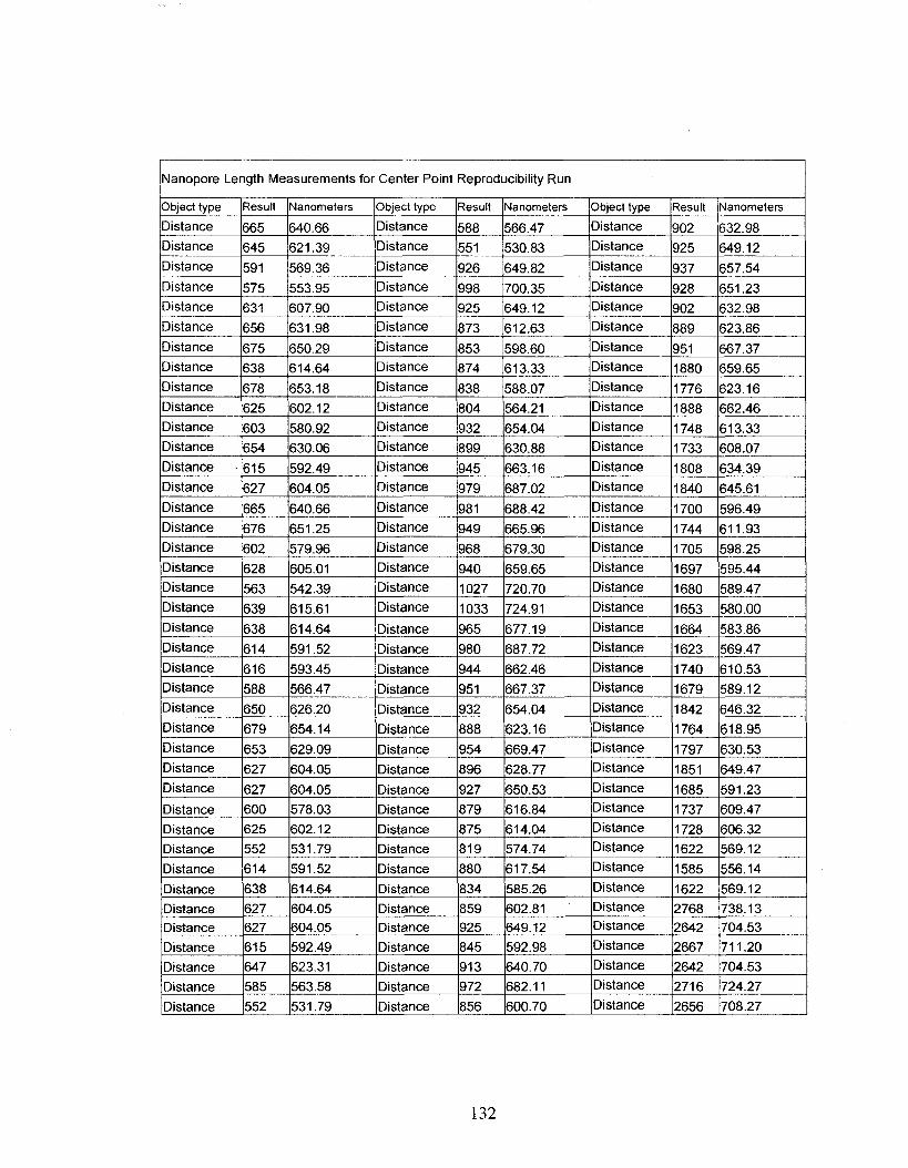
Nanopore Length Measurements for Center Point Reproducibility Run
Object type
Distance
Distance
Distance
Distance
Distance
Distance
Distance
Distance
Distance
Distance
Distance
Distance
Distance
Distance
Distance
Distance
Distance
Distance
Distance
Distance
Distance
Distance
Distance
Distance
Distance
Distance
Distance
Distance
Distance
Distance
Distance
Distance
Distance
Distance
Distance Distance
Distance
Distance
Distance
Distance
Result
665
645
591
575
631
656
675
638
678
625
603
654
615
627
665
676
602
628
563
639
638
614
616
588
650
679
653
627
627
600
625
552
614
638
627 627
615
647
585
552
Nanometers
640.66
621.39
569.36
553.95
607.90
631.98
650.29
614.64
653.18
602.12
580.92
630.06
592.49
604.05
640.66
651.25
579.96
605.01
542.39
615.61
614.64
591.52
593.45
566.47
626.20
654.14
629.09
604.05
604.05
578.03
602.12
531.79
591.52
614.64
604.05 604.05
592.49
623.31
563.58
531.79
Object type
Distance
Distance
Distance
Distance
Distance
Distance
Distance
Distance
Distance
Distance
Distance
Distance
Distance
Distance
Distance
Distance
Distance
Distance
Distance
Distance
Distance
Distance
Distance
Distance
Distance
Distance
Distance
Distance
Distance
Distance
Distance
Distance
Distance
Distance
Distance Distance
Distance
Distance
Distance
Distance
Result
588
551
926
998
925
873
853
874
838
804
932
899
945
979
981
949
968
940
1027
1033
965
980
944
951
932
888
954
896
927
879
875
819
880
834
859 925
845
913
972
856
Nanometers
566.47
530.83
649.82
700.35
649.12
612.63
598.60
613.33
588.07
564.21
654.04
630.88
663.16
687.02
688.42
665.96
679.30
659.65
720.70
724.91
677.19
687.72
662.46
667.37
654.04
623.16
669.47
628.77
650.53
616.84
614.04
574.74
617.54
585.26
602.81 649.12
592.98
640.70
682.11
600.70
Object type
Distance
Distance
Distance
Distance
Distance
Distance
Distance
Distance
Distance
Distance
Distance
Distance
Distance
Distance
Distance
Distance
Distance
Distance
Distance
Distance
Distance
Distance
Distance
Distance
Distance
Distance
Distance
Distance
Distance
Distance
Distance
Distance
Distance
Distance
Distance Distance
Distance
Distance
Distance
Distance
Result
902
925
937
928
902
889
951
1880
1776
1888
1748
1733
1808
1840
1700
1744
1705
1697
1680
1653
1664
1623
1740
1679
1842
1764
1797
1851
1685
1737
1728
1622
1585
1622
2768 2642
2667
2642
2716
2656
Nanometers
632.98
649.12
657.54
651.23
632.98
623.86
667.37
659.65
623.16
662.46
613.33
608.07
634.39
645.61
596.49
611.93
598.25
595.44
589.47
580.00
583.86
569.47
610.53
589.12
646.32
618.95
630.53
649.47
591.23
609.47
606.32
569.12
556.14
569.12
738.13 704.53
711.20
704.53
724.27
708.27
132

Nanopore Length Measurements for Center Point Reproducibility Run
Object type
Distance
Distance
Distance
Distance
Distance
Distance
Distance
Distance
Distance
Distance
Distance
Distance
Distance
Distance
Result
2642
2626
2723
2559
2576
2458
2454
2597
2476
2497
2375
2430
2477
2305
Nanometers
704.53
700.27
726.13
682.40
686.93
655.47
654.40
692.53
660.27
665.87
633.33
648.00
660.53
614.67
133

Appendix M. 0°C Substrate Data
134

SEM Images for 0°C Substrate
100 K 100nm = 938nm
13K 1 urn = 1025 i m
20 K 500 nm = 938 urn
25 K 500 nm = 1188 p.m
45 K 200 nm = 850 |am
135

Diameter Measurements for 0° C Run
Object type
Diameter
Diameter
Diameter
Diameter
Diameter
Diameter
Diameter
Diameter
Diameter
Diameter
Diameter
Diameter
Diameter
Diameter
Diameter
Diameter
Diameter
Diameter
Diameter
Diameter
Diameter
Diameter
Diameter
Diameter
Diameter
Diameter
Diameter
Diameter
Diameter
Diameter
Diameter
Diameter
Diameter
Diameter
Diameter
Diameter
Diameter
Diameter
Diameter
Diameter
Result
283
270
230
273
250
284
303
292
240
311
292
272
248
267
298
251
279
241
266
269
285
311
343
308
365
258
302
259
385
332
355
299
324
325
321
280
284
319
227
293
Nanometers
37.73
36.00
30.67
36.40
33.33
37.87
40.40
38.93
32.00
41.47
38.93
36.27
33.07
35.60
39.73
33.47
37.20
32.13
35.47
35.87
38.00
41.47
45.73
41.07
48.67
34.40
40.27
34.53
51.33
44.27
47.33
39.87
43.20
43.33
42.80
37.33
37.87
42.53
30.27
39.07
Object type
Diameter
Diameter
Diameter
Diameter
Diameter
Diameter
Diameter
Diameter
Diameter
Diameter
Diameter
Diameter
Diameter
Diameter
Diameter
Diameter
Diameter
Diameter
Diameter
Diameter
Diameter
Diameter
Diameter
Diameter
Diameter
Diameter
Diameter
Diameter
Diameter
Diameter
Diameter
Diameter
Diameter
Diameter
Diameter
Diameter
Diameter
Diameter
Diameter
Diameter
Result
273
285
313
330
344
298
299
298
288
336
359
290
303
245
266
337
249
361
307
285
326
277
313
306
284
203
193
155
194
234
154
165
163
182
156
176
200
192
189
156
Nanometers
36.40
38.00
41.73
44.00
45.87
39.73
39.87
39.73
38.40
44.80
47.87
38.67
40.40
32.67
35.47
44.93
33.20
48.13
40.93
38.00
43.47
36.93
41.73
40.80
37.87
43.28
41.15
33.05
41.36
49.89
32.84
35.18
34.75
38.81
33.26
37.53
42.64
40.94
40.30
33.26
Object type
Diameter
Diameter
Diameter
Diameter
Diameter
Diameter
Diameter
Diameter
Diameter
Diameter
Diameter
Diameter
Diameter
Diameter
Diameter
Diameter
Diameter
Diameter
Diameter
Diameter
Diameter
Diameter
Diameter
Diameter
Diameter
Diameter
Diameter
Diameter
Diameter
Diameter
Diameter
Diameter
Diameter
Diameter
Diameter
Diameter
Diameter
Diameter
Diameter
Diameter
Result
178
147
169
158
165
208
196
138
157
165
173
211
170
171
137
149
186
232
130
179
170
180
143
178
217
160
163
163
174
144
172
197
164
196
206
183
179
221
179
203
Nanometers
37.95
31.34
36.03
33.69
35.18
44.35
41.79
29.42
33.48
35.18
36.89
44.99
36.25
36.46
29.21
31.77
39.66
49.47
27.72
38.17
36.25
38.38
30.49
37.95
46.27
34.12
34.75
34.75
37.10
30.70
36.67
42.00
34.97
41.79
43.92
39.02
38.17
47.12
38.17
43.28
136

Diameter Measurements for 0° C Run
Object type
Diameter
Diameter
Diameter
Diameter
Diameter
Diameter
Diameter
Diameter
Diameter
Diameter
Diameter
Diameter
Diameter
Diameter
Diameter
Diameter
Diameter
Diameter
Diameter
Diameter
Diameter
Diameter
Diameter
Diameter
Diameter
Diameter
Diameter
Diameter
Diameter
Diameter
Diameter
Diameter
Diameter
Diameter
Diameter
Diameter
Diameter
Diameter
Diameter
Diameter
Result
178
132
163
221
219
176
172
178
204
208
164
133
144
124
169
169
150
134
137
116
151
124
113
159
162
174
179
159
128
144
187
153
167
151
160
157
178
178
133
179
Nanometers
37.95
28.14
34.75
47.12
46.70
37.53
36.67
37.95
43.50
44.35
43.73
35.47
38.40
33.07
45.07
45.07
40.00
35.73
36.53
30.93
40.27
33.07
30.13
42.40
43.20
46.40
47.73
42.40
34.13
38.40
49.87
40.80
44.53
40.27
42.67
41.87
47.47
47.47
35.47
47.73
Object type
Diameter
Diameter
Diameter
Diameter
Diameter
Diameter
Diameter
Diameter
Diameter
Diameter
Diameter
Diameter
Diameter
Diameter
Diameter
Diameter
Diameter
Diameter
Diameter
Diameter
Diameter
Diameter
Diameter
Diameter
Diameter
Diameter
Diameter
Diameter
Diameter
Diameter
Diameter
Diameter
Diameter
Diameter
Diameter
Diameter
Diameter
Diameter
Diameter
Diameter
Result
152
170
190
155
189
144
181
161
176
183
149
160
155
159
149
158
141
171
201
168
151
191
172
165
164
166
168
158
170
164
184
151
153
149
157
249
228
242
420
317
Nanometers
40.53
45.33
50.67
41.33
50.40
38.40
48.27
42.93
46.93
48.80
39.73
42.67
41.33
42.40
39.73
42.13
37.60
45.60
53.60
44.80
40.27
50.93
45.87
44.00
43.73
44.27
44.80
42.13
45.33
43.73
49.07
40.27
40.80
39.73
41.87
26.55
24.31
25.80
44.78
33.80
Object type
Diameter
Diameter
Diameter
Diameter
Diameter
Diameter
Diameter
Diameter
Diameter
Diameter
Diameter
Diameter
Diameter
Diameter
Diameter
Diameter
Diameter
Diameter
Diameter
Diameter
Diameter
Diameter
Diameter
Diameter
Diameter
Diameter
Diameter
Diameter
Diameter
Diameter
Diameter
Diameter
Diameter
Diameter
Diameter
Diameter
Diameter
Diameter
Diameter
Diameter
Result
174
168
185
239
308
280
235
241
321
290
214
310
309
347
204
193
231
314
356
294
292
167
244
210
290
187
218
280
281
294
192
324
280
285
353
284
334
199
344
145
Nanometers
18.55
17.91
19.72
25.48
32.84
29.85
25.05
25.69
34.22
30.92
22.81
33.05
32.94
36.99
21.75
20.58
24.63
33.48
37.95
31.34
31.13
17.80
26.01
22.39
30.92
19.94
23.24
29.85
29.96
31.34
20.47
34.54
29.85
30.38
37.63
30.28
35.61
21.22
36.67
15.46
137

Nanopore Length Measurements for 0° C Run
Object type
Distance
Distance
Distance
Distance
Distance
Distance
Distance
Distance
Distance
Distance
Distance
Distance
Distance
Distance
Distance
Distance
Distance
Distance
Distance
Distance
Distance
Distance
Distance
Distance
Distance
Distance
Distance
Distance
Distance
Distance
Distance
Distance
Distance
Distance
Distance
Distance
Distance
Distance
Distance
Distance
Result
539
563
569
565
532
522
540
578
541
564
551
547
539
553
553
600
526
529
518
521
514
554
520
514
516
547
520
609
526
576
653
679
532
517
559
531
946
984
955
956
Nanometers
525.85
549.27
555.12
551.22
519.02
509.27
526.83
563.90
527.80
550.24
537.56
533.66
525.85
539.51
539.51
585.37
513.17
516.10
505.37
508.29
501.46
540.49
507.32
501.46
503.41
533.66
507.32
594.15
513.17
561.95
637.07
662.44
519.02
504.39
545.37
518.05
504.26
524.52
509.06
509.59
Object type
Distance
Distance
Distance
Distance
Distance
Distance
Distance
Distance
Distance
Distance
Distance
Distance
Distance
Distance
Distance
Distance
Distance
Distance
Distance
Distance
Distance
Distance
Distance
Distance
Distance
Distance
Distance
Distance
Distance
Distance
Distance
Distance
Distance
Distance
Distance
Distance
Distance
Distance
Distance
Distance
Result
963
1023
944
1014
968
967
961
1046
979
1020
1026
1017
955
942
960
979
941
955
940
983
993
1010
939
951
992
955
983
1005
973
998
971
962
1051
938
1663
1564
1526
1550
1475
1510
Manometers
513.33
545.31
503.20
540.51
515.99
515.46
512.26
557.57
521.86
543.71
546.91
542.11
509.06
502.13
511.73
521.86
501.60
509.06
501.07
523.99
529.32
538.38
500.53
506.93
528.78
509.06
523.99
535.71
518.66
531.98
517.59
512.79
560.23
500.00
699.92
658.25
642.26
652.36
620.79
635.52
Object type
Distance
Distance
Distance
Distance
Distance
Distance
Distance
Distance
Distance
Distance
Distance
Distance
Distance
Distance
Distance
Distance
Distance
Distance
Distance
Distance
Distance
Distance
Distance
Distance
Distance
Distance
Distance
Distance
Distance
Distance
Distance
Distance
Distance
Distance
Distance
Distance
Distance
Distance
Distance
Result
1481
1316
1312
1365
1361
1368
1163
1322
1371
1356
1238
1372
1355
1335
1275
1805
1228
1354
1374
1318
1688
2243
2091
2121
2200
2110
2097
2079
1991
1791
2012
1971
1996
1885
1915
1789
1780
1932
1694
Nanometers
623.32
553.87
552.19
574.49
572.81
575.76
489.48
556.40
577.02
570.71
521.04
577.44
570.29
561.87
536.62
759.68
516.84
569.87
578.28
554.71
710.44
944.02
880.05
565.60
586.67
562.67
559.20
554.40
530.93
477.60
536.53
525.60
532.27
502.67
510.67
477.07
474.67
515.20
451.73
138