Embed Size (px)
Citation preview

JOHANNES KEPLER
UNIVERSITY LINZ
Altenberger Str 69
4040 Linz Austria
wwwjkuat
DVR 0093696
Submitted by
Dorian Ziss
Submitted at
Institute of Semiconductor
and Solid State Physics
Supervisor
Julian Stangl
10-2017
X-ray Diffraction vs
Photoluminescence
of
Semiconductor -
Nanostructures
Master Thesis
to obtain the academic degree of
Diplom-Ingenieur
in the Masterrsquos Program
Nanoscience and -Technology
September 22 2017 Dorian 2103
September 22 2017 Dorian 3103
STATUTORY DECLARATION
I hereby declare that the thesis submitted is my own unaided work that I have not used other
than the sources indicated and that all direct and indirect sources are acknowledged as
references
This printed thesis is identical with the electronic version submitted
Linz October 2017
September 22 2017 Dorian 4103
September 22 2017 Dorian 5103
Acknowledgements
The success and outcome of this thesis required a lot of guidance and assistance from many
people and I am extremely privileged to have got this all along the completion of the thesis
Therefore I want to seize the opportunity to thank everyone who contributed and helped me finish
this thesis and lastly also my studies
My first and special thanks go to my supervisor Julian Stangl who always had time for me in all
matters although he had to face turbulent times All that I have done was only possible due to his
enthusiastic supervision and assistance
I highly respect and thank Javier Martiacuten Saacutenchez for providing me with the opportunity to learn
about various fabrication techniques in the cleanroom and for giving me all support and guidance
although he had a busy schedule managing and training many students
I also owe my gratitude to the head of our institute Armando Rastelli as well as to Thomas Lettner
Rinaldo Trotta and Friedrich Schaumlffler who always took keen interest in our concerns and
problems and guided us all along whenever it was needed
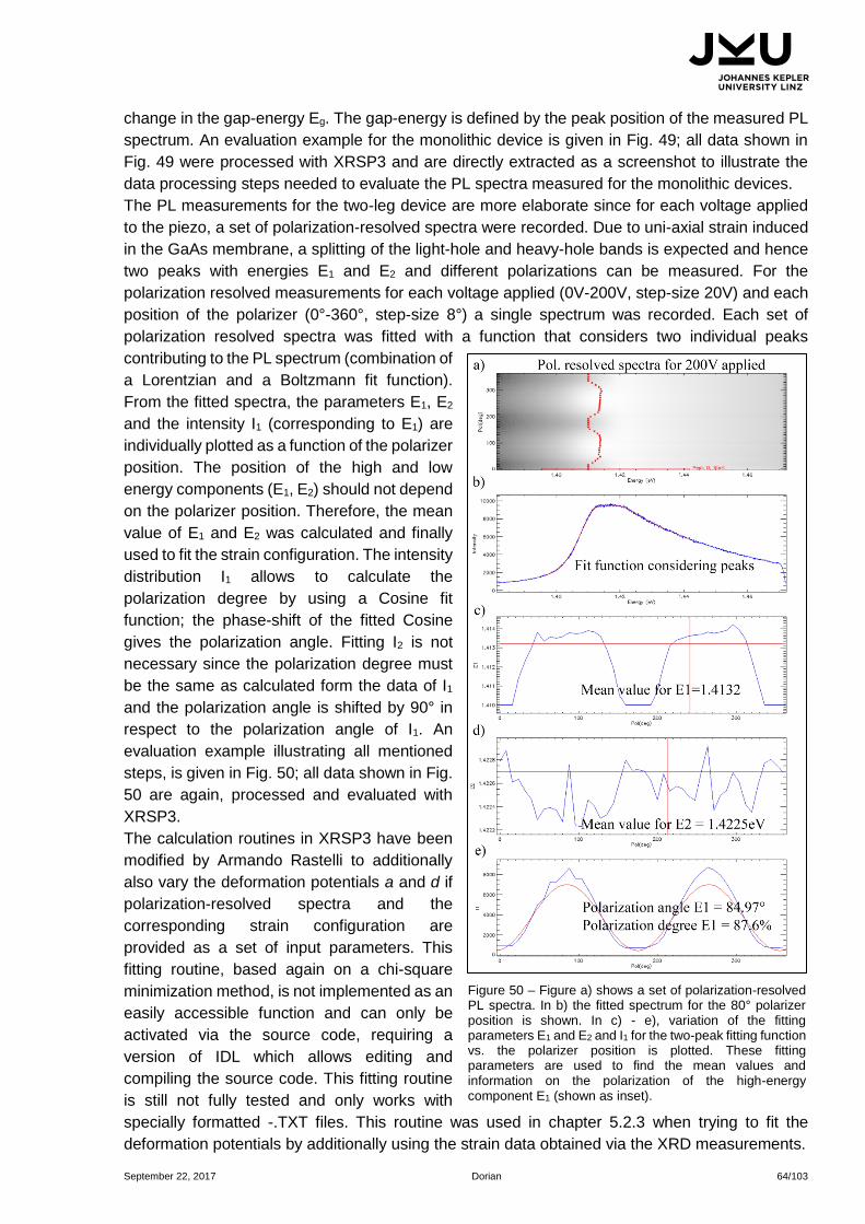
Furthermore I should not forget to mention Marc Watzinger Elisabeth Lausecker and Stefanie
Siebeneichler as well as all former and recent colleagues in the office for their encouragement
and moreover for their timely support and guidance until the completion of this thesis
I heartily thank the whole team of the Semiconductor amp Solid State Physics department and
especially Ernst Vorhauer for their support whenever necessary
Finally and most importantly I am very thankful and fortunate to get constant encouragement
support and guidance from my family and specially from my partner in life Bettina Berger who
might have suffered most during the time when I was working on this thesis and related projects
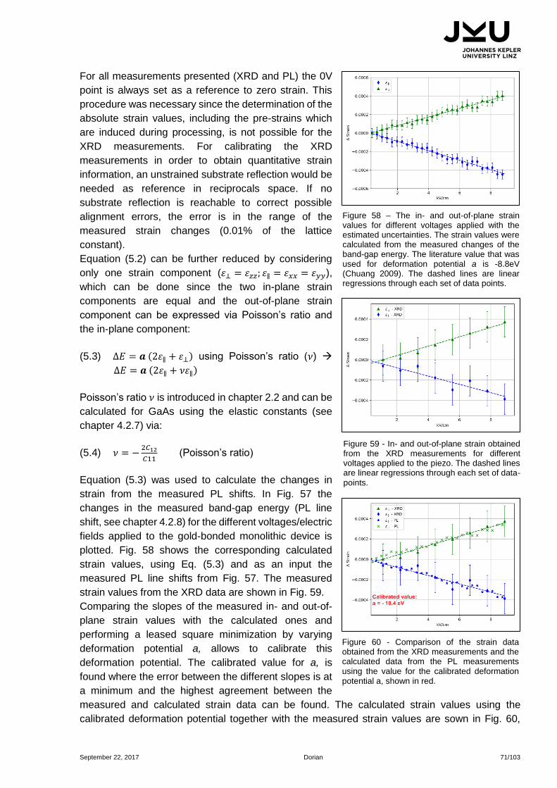
September 22 2017 Dorian 6103
Contents
1 Introduction 9
2 Theory 12
21 Theory of X-ray scattering 12
211 Electromagnetic waves ndash Maxwellrsquos equations 12
212 Generation of X-rays 13
213 Interaction of X-rays with matter 17
214 X-ray scattering on free electrons 18
215 The atomic form factor scattering on atoms 20
216 The structure factor scattering on molecules and crystals 21
217 The reciprocal space Bragg- and Laue-condition 21
218 Refraction and reflection Snellrsquos law for X-rays 23
219 Scanning the reciprocal space by measuring angles and intensities 25
22 Generalized Hookrsquos law the theory of strain and stress 28
221 Introducing the concept of strainstress for isotropic materials 28
222 The elasticity tensor for un-isotropic materials 29
23 Basics of photoluminescence 31
231 Band structure of GaAs 31
232 The effect of stressstrain on the band structure 34
24 Basics of X-ray excited optical luminescence (XEOL) 37
25 Piezoelectric materials 38
251 Properties of PMN-PT 40
3 Device layouts and fabrication 42
31 Investigated samples 42
311 Monolithic device 42
312 Two-leg device 43
32 Fabrication process 43
321 Gold-thermo-compression 45
322 SU8 mediated bonding 45
4 The experiment 46
41 Experimental setups 46
411 XRD-Setup 46
412 PL-Setup 48
413 Synchrotron setup for XRD and XEOL 49
42 Measurements evaluation and data treatment 51
September 22 2017 Dorian 7103
421 Symmetric and asymmetric reflections in two azimuths 51
422 Symmetric reflections used for tilt correction 53
423 Position resolved RSMs 55
425 Footprint strain and tilt distribution 57
426 Track changes with COM calculations 59
427 Tilt varies faster than strain symmetric reflection is the reference 61
428 PL-data ndash Measurements and evaluation 63
5 Results and discussion 65
51 Monolithic devices 65
511 Comparing different bonding techniques ndash Experimental part 65
512 Comparing different bonding techniques - Simulations 67
513 Calibrating the deformation potential XRD vs PL line shift 70
52 Two-leg device 73
521 Calibrating deformation potentials XRD vs PL line shift 73
522 Discussion of nano-focused beam measurements 76
523 Evaluation of the XEOL measurements 80
6 Summary and outlook 86
7 Appendix 89
71 Python code 89
711 Tilt calculation 89
712 Image processing filters 89
713 Centre-of-mass-calculations routines used for 2D and 3D RSMs 90
72 Reciprocal space maps (RSMs) 93
721 RSMs ndash Monolithic device ndash Gold bonding 93
722 RSMs ndash Monolithic device ndash SU8 bonding 94
723 RSMs ndash Two-leg device 95
724 3D -RSMs ndash Two-leg device - Synchrotron 97
Abbreviations and shortcuts 99
References 100
September 22 2017 Dorian 8103
September 22 2017 Dorian 9103
1 Introduction
Nano-structured semiconductors such as quantum dots (QDs) are very promising for the
realization of light sources used in modern optical applications The QDs offer the possibility to
build single photon sources which can emit single photons on demand The single photon sources
are needed for communication protocols using quantum mechanical properties for encrypted
transfer of information that is intrinsically safe against eavesdropping The most important aspect
in this context is the ability to create single indistinguishable photons which can then be entangled
One problem using QD as the source for single photons is that they have to some extent
ldquostatisticallyrdquo deviating properties after growth via molecular beam epitaxy such as a slightly
different chemical composition or a varying size and strain distribution Thus their ldquoatom-likerdquo
energy states differ slightly from dot to dot and the emitted photons are hence not indistinguishable
anymore To overcome this problem there are generally two possibilities The first one which is
not suitable for integrated devices and rather time-consuming is to simply search for two QDs
with the same intrinsic properties The second possibility is to modify the emission properties of
the QD The first possibility is of course always applicable but there is no guarantee to find two
identical dots Hence the second possibility tuning the energy levels of a QD after growth is the
smarter but more sophisticated solution to overcome this problem Possible ldquotuning-knobsrdquo are
either electricmagnetic fields or strain Several works have been published in the past
demonstrating that the energy levels (band-structure) of QDs can be successfully tuned via strain
electric fields or a combination of both (Trotta et al 2012 Huo et al 2013 Zhang et al 2013
Trotta et al 2015 Martiacuten-Saacutenchez et al 2016 Kremer et al 2014) In this thesis we will focus on
strain which can be used as a ldquotuning knobrdquo for the energy levels The QDs used in this context
are InGaAs QDs embedded in a GaAs matrix which is effectively a 400 nm thick membrane To
get active and reproducible control on the strain state the GaAs membrane is bonded onto a
piezoelectric substrate This configuration allows reversibly inducing strain by applying a voltage
to the piezoelectric substrate with the GaAs membrane on top following the deformation of the
piezo actuator
One particular challenge is that the induced strain in the GaAs cannot be measured precisely from
the optical response of the material (line shift of the GaAs emission) Although the relations
between the strain tensor and the induced changes in the energy levels and band-structure are
theoretically well developed (Chuang 2009) they still rely on material parameters ndash so-called
optical deformation potentials - which are only known to a certain extent (Vurgaftman et al
2001)The colleagues from the institute of semiconductor physics at JKU (Linz) could in principal
determine the effective strain configuration induced in the GaAs just measuring the emission
characteristics extremely accurately (changes in the crystal lattice of about 10-4Å) The most
limiting factors as mentioned are the deformation potentials which can easily deviate by plusmn20
(depending on the particular deformation potential) Hence it is necessary to use a direct method
to get accurate information about the induced strain state without having the problem of intrinsically
high errors Furthermore from the optical measurements alone it is not possible to estimate the
amount of strain that is effectively produced by the piezo actuator which is a benchmark for the
capability of the devices
In this thesis we wanted to find answers to some of the issues which cannot be answered using
only the optical characterization of the devices which have been carried out by our colleagues in
the past Therefore we used X-ray diffraction (XRD) as a technique to get direct information on
the lattice constants in the material and hence information on the induced strain states The first
aim of this work is to investigate how the strain is transferred from the piezo via different bonding
layers to the GaAs and hence to the QDs A second aim is to provide a reliable set of material
September 22 2017 Dorian 10103
parameters (optical deformation potentials) linking the mechanical and optical properties This is
done by comparing the strain measured by X-ray diffraction to the calculated strain form the
changes of the optical emissions and optimizing the deformation potentials to reduce the
differences between calculated and measured strain values
Ultimately this would require measurements by XRD and PL at exactly the same QD under exactly
the same conditions (piezo voltage measurement temperature etc) Such an experiment is
currently not feasible due to a limited resolution of the probing X-rays As a first step we therefore
have performed strain and optical measurements on the GaAs membrane and not on the individual
QDs since the strain state of the QDs follows the induced strain in the membrane With this
approach it was possible to show the feasibility of the experiments and already establish
experimental routines for the final aim which will need to involve X-ray diffraction using nano-
focused synchrotron radiation combined with X-ray excited optical luminescence at cryogenic
temperature On the way we have investigated the strain transfer from the piezo to the membrane
with some unexpected and on first sight counter-intuitive results
The experiments described can be divided into experiments done in our lab and experiments
performed using synchrotron radiation at the ESRF (European Synchrotron Radiation Facility) in
Grenoble France The synchrotron measurements became important when investigating more
complicated structured piezo actuators (Martiacuten-Saacutenchez et al 2016 Trotta et al 2016) which
allow inducing strains with different in-plane orientations Those devices could not properly be
investigated in our X-ray lab due to the limited lateral resolution of the X-ray beam For the optical
experiments in contrast the resolution is just limited by the wavelength of the light-source used
for excitation The problem of having different spot sizes and hence probing different positions on
the same sample makes a valid comparison of PL and XRD measurements complicated To
overcome this discrepancy we employed the focused synchrotron radiation where X-ray spot
sizes in the 500 nm range could be achieved which are even smaller than the spot sizes used for
optical excitation in the lab The synchrotron radiation additionally offers the possibility to measure
XRD and the optical emission in exactly the same sample state This is possible because the
intense and focused high energy X-ray photons induce X-ray excited optical luminescence (XEOL)
in the GaAs membrane The advantage in comparison to the lab measurements is that it is not
necessary to change the setup or move the sample At the synchrotron it is possible to measure
at the same time using only one excitation source for both signals the diffracted X-rays and the
excited photoluminescence Whereas in the lab the sample has to be unmounted from the XRD
setup and re-installed at the optical setup which unavoidably leads to certain changes in the
position that is probed on the sample
For the experiments done in the lab and at the synchrotron many experimental challenges had to
be solved The problems started when investigating the piezo substrates and the GaAs
membranes which did not show a single crystalline behaviour although both were assumed to be
nearly perfect single crystals Distortions and the contribution of different domains to the diffracted
signal lead to a broadening of the Bragg peaks measured via XRD in reciprocal space This made
an accurate determination of the lattice constant rather complicated To be able to resolve and
track differences in the lattice constant which are in the order of 10-3Aring the measurement process
was optimized and a data evaluation procedure which allows a reproducible tracking of the
changes was established
The XRD lab measurements presented in this thesis were used to quantify the effective strain
transfer from the deformed piezo actuator to the GaAs membrane For this purpose using two
different well-established bonding techniques were compared We could successfully explain the
measured differences in the strain transfer by investigating the complicated bonding mechanisms
using finite element method (FEM) simulations for modelling the bonding-interfaces We can say
September 22 2017 Dorian 11103
that the efficiencies we have measured are one of the highest that have been reported for
materials strained in-situ with piezo actuators
In addition a comparison of the XRD data and the measured changes in the PL spectra for various
voltages applied to the actuator allowed for simple and highly symmetric strain configurations to
successfully re-calculate the deformation potential Although a first re-calculation was successful
the error in the measurements was still too high to achieve a valid calibration of the material
parameters This was one of the reasons to perform the same kind of experiments at the
synchrotron For the synchrotron measurements the error was assumed to be much smaller since
the diffracted X-ray beam and the optical luminescence (XEOL) were measured simultaneously
Although the XEOL measurements were very puzzling and not fully successful it could be proven
that XEOL spectra with reasonably high intensities similar to PL measurements in the lab can be
recorded while simultaneously performing XRD measurements which had not been clear at this
point The nano-focused XRD measurements performed at synchrotron additionally showed that
the effective strain- and tilt-distribution of the GaAs membrane is rather complicated and far off a
perfectly modelled system as it was expected to be These results on the other hand were very
helpful to explain the lab measurements where only global changes in strain could be measured
due to the larger beam-spot size
This thesis is divided into six main chapters (including the introduction) It starts with the theoretical
description of the used techniques and mechanisms Within this chapter X-ray diffraction as a
technique to measure interatomic distances in crystalline materials is explained as well as the
theoretical concepts which link the optical properties to the crystal structure using the deformation
potentials Furthermore mechanisms behind XEOL which are relevant when measuring at the
synchrotron and the properties of the piezoelectric material used as actuator are explained In the
next chapter chapter 3 details on the investigated devices (fabrication process propertieshellip) are
presented Chapter 4 is attributed to the experimental details including the XRD and PL
measurements performed in the lab and at the synchrotron Each setup used is explained in detail
together with the data evaluation procedure which was highly relevant for the success of the
experiments Chapter 5 explains and discusses the results for each individual device that was
characterized optically and via XRD By comparing both types of measurements also the
recalculated values for the deformation potentials are discussed in this chapter In the very last
chapter an outlook for further improvements and future projects is given
September 22 2017 Dorian 12103
2 Theory
21 Theory of X-ray scattering
211 Electromagnetic waves ndash Maxwellrsquos equations
This chapter gives an introduction to the basics of X-rays by shortly explaining the most relevant
aspects in terms of electromagnetic radiation their creation and their interaction with matter
X-rays are part of the electromagnetic spectrum and hence can be described as electromagnetic
waves Talking about X-rays the relevant wavelength scale is in the range of 0002 x 10-10m (ultra-
hard X-rays) up to 200 x 10-10m (soft X-rays where the lower end of the UV (ultra-violet) spectrum
starts) Looking at X-ray diffraction the wave-like character of light is the key to understand the
relevant scattering and diffraction processes
In general all electromagnetic waves have to fundamentally obey the electromagnetic wave
equation which can easily be derived starting from Maxwellrsquos equations describing electro-
dynamical processes and assuming that no free charges (120588 = 0) and electrical currents (119895 = 0)
are present The four Maxwellrsquos equations then simplify to
(21) nabla middot = 0 (Gaussrsquos law assuming 120588 = 0)
(22) nabla middot = 0 (Gaussrsquos law for magnetism)
(23) nabla times = minuspart
partt (Farradayrsquos law of induction)
(24) nabla times = 휀01205830part
partt (Amperersquos law assuming 119895 = 0)
Applying the differential operator rot (see appendix) on both sides of Eq (23) and Eq (24) leads
to the so-called wave-equations which must hold for all electromagnetic waves
(25) nabla times (nabla times ) = minuspart
parttnabla times = minus 휀01205830
part2
part1199052 rarr 0 =1
1198882
part2
part1199052 minus ∆
(26) nabla times (nabla times ) = 휀01205830part
parttnabla times = minus 휀01205830
part2
part1199052 rarr 0 =1
1198882
part2
part1199052 minus ∆
The constant c is the speed of light in vacuum and 휀0 the permittivity and 1205830 the permeability in
vacuum They are connected via
(27) 119888 =1
radic12057601205830
Many waves satisfy the electromagnetic wave equations in (25) and (26) but we will focus on
spherical or plane waves When starting with the concepts of scattering and diffraction we will
again refer to these types of waves The electric and magnetic field component of a plane wave
can be described by
(28) = 0ei(119903minusωt) Plane-Wave oscillating of E-field
(29) = 0ei(119903minusωt) Plane-Wave oscillating of B-field
September 22 2017 Dorian 13103
In Eq (28) and (29) is called the wave-vector which points in the direction of propagation The
phase of the plane wave is defined as Φ = 119903 minus ωt with Φ = const ω = 119888|| The length of the
vector for a freely propagating wave is constant and can be written as =2120587
120582 It follows that the
wavelength 120582 and the angular frequency 120596 = 2120587119891 are constant and the energy of each X-ray
photon (basically every photon) can be calculated by
(210) E = ℏ middot ω = h middot f = ℎmiddotc
120582
Eq (210) states that the energy of the photon is proportional to the frequency of the radiation and
indirectly proportional to the wavelength
212 Generation of X-rays
This section will explain in short how X-rays are generated in the context of lab sources and the
differences to the generation of X-rays at a synchrotron radiation facility
Electromagnetic radiation is in the most general description generated if charged particles are
accelerated (indicated by the second derivative of time in Eq (25) and (26)) Having this in mind
and now looking at usual lab sources X-rays are typically generated by accelerating electrons out
of a cathode onto an anode metal-block The cathode is usually a heated filament and the anode
is a solid metal-block mostly copper tungsten or molybdenum When the electrons hit the target
they lose their kinetic energy which can be explained by an acceleration process with negative
sign This process always creates a continuous X-ray spectrum called ldquobremsstrahlungrdquo with a
low-wavelength on-set depending on the maximum electron energy (see Fig 1) The kinetic
energy of the electrons is defined by the acceleration voltage see Eq (211)
(211) 119864119896119894119899 = e middot V = 119898middot1199072
2
If the kinetic energy of the electron exceeds a certain
energy threshold value resonances in the X-ray spectrum
can be observed on-top of the white radiation spectrum
These resonances can be seen as very sharp and intense
lines superimposed on the continuous spectrum They are
called characteristic lines because their position in energy
depends on the anode material That means each anode
material shows a set of characteristic lines unique in
wavelength and energy The appearance of these resonant
lines can be understood by the excitation of K L M
(different electron shells which correspond to the principal
quantum numbers of n=123) electrons which during the
relaxation process emit only radiation in a very narrow
wavelength region corresponding to the energy of the
originally bound electron The short wavelength onset
which has already been mentioned corresponds in terms of energy to the maximum electron
energy which can be converted directly without losses into X-ray radiation This onset can be
calculated using Eq (210) and (211) to
(212) 120582119900119899119904119890119905 =ℎmiddotc
119890middot119881
Figure 1 - Characteristic radiation of a molybdenum target for different electron
energies (Cullity 1978 S 7)
September 22 2017 Dorian 14103
Fig 1 shows the characteristic emission spectrum from a
molybdenum target for different electron energies (measured in
keV)
In Fig 2 one can see the most probable transitions and their
nomination The first letter defines the final shell (K L Mhellip)
and the suffix (α βhellip) the initial shell For instance Kα
means that an electron from the L (n=2) shell undergoes a
radiative transition to the first shell K (n=1) If one zooms
further into the characteristic K or L lines one will see that it
is not one single line in fact they consist of two individual
lines called the doublets for instance Kα1 and Kα2 The
splitting into individual lines can be understood by
considering also different possible orientations for the orbital
angular momentum of the electrons involved in the transition called the fine structure
splitting
In 1913 Henry Moseley discovered an empiric law to calculate the energy of the
characteristic transitions for each element This was historically very important because it
was a justification of Bohrrsquos predicted concept of an atom Moseley originally discovered
his law for the characteristic Kα X-ray emission line which was the most prominent line in
terms of brightness but in general terms this law is valid for each possible (and allowed)
transition see Eq (213) and (214)
(213) 119864119901ℎ119900119905119900119899 = 119891119901ℎ119900119905119900119899 lowast ℎ = 119864119894 minus 119864119891 =119891119877lowast119885119890119891119891
2
ℎ[
1
1198991198912 minus
1
1198991198942] Moseleyrsquos law
(214) 119891119877 =119898119890119890
4
812057602ℎ2 lowast
1
1+119898119890119872
expanded Rydberg-frequency
In Eq (213) Zeff is the effective charge of the nucleus which means it is the atomic number
Z reduced by a factor S which is proportional to the number of electrons shielding the
nucleus at the point of interest Ephoton and fphoton are the energy and the frequency of the
emitted photon and the letters i and f should indicate the initial and the final state of the
transition together with n the principal quantum number For a Kα transition this would
mean that nf = 2 and ni = 1 Eq (214) shows the expanded Rydberg-frequency used in
Eq (213) where M denotes the mass of the nucleus
The process of X-ray generation where the electrons directly interact with the target
atoms is as discussed before widely used for lab sources such as Coolidge-tubes and
Rotating-anode or Metal-jet setups A more detailed discussion on the X-ray source used
for the experiments is given in chapter 4
The important parameter which characterizes the quality of an X-ray source and hence
also sets an intrinsic limit for the resolution obtainable in diffraction experiments is the
brilliance of a light-source (source for X-ray) defined as
(215) 119887119903119894119897119897119894119886119899119888119890 = 119901ℎ119900119905119900119899119904
119904119890119888119900119899119889lowast
1
1198981199031198861198892 lowast 1198981198982 lowast 01 119861119882
Where mrad2 defines the angular divergence in milli-radiant the source-area is given in
mm2 and the last term (01 BW) denominates the photons falling in relative bandwidth
(BW) of 01 of the chosen wavelength which is a measure for the spectral distribution
Figure 2 - Illustration for the most relevant transitions in terms of X-ray generation
September 22 2017 Dorian 15103
of the emitted photons The given brilliance of a
source already includes the influences of all beam
collimating and shaping elements like mirror-optics
monochromators or apertures Achievable
brilliances for lab sources are in the order of 107-
108 (Eberhardt 2015)
If higher brilliances are needed to successfully
perform the experiments one has to use large
scale facilities dedicated to the production of X-rays
with extremely high brilliances over a large spectral
range known as synchrotron light sources The X-
ray generation on synchrotrons is different to the
generation using lab sources because no direct
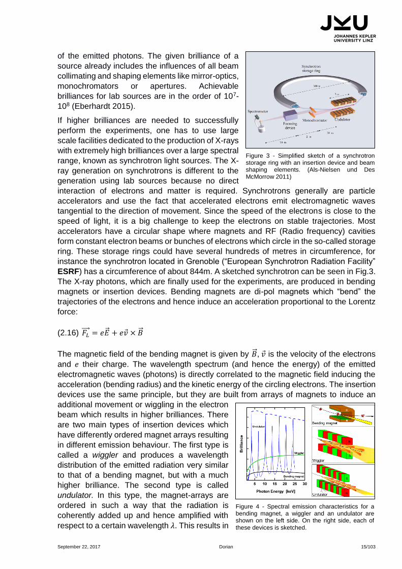
interaction of electrons and matter is required Synchrotrons generally are particle
accelerators and use the fact that accelerated electrons emit electromagnetic waves
tangential to the direction of movement Since the speed of the electrons is close to the
speed of light it is a big challenge to keep the electrons on stable trajectories Most
accelerators have a circular shape where magnets and RF (Radio frequency) cavities
form constant electron beams or bunches of electrons which circle in the so-called storage
ring These storage rings could have several hundreds of metres in circumference for
instance the synchrotron located in Grenoble (ldquoEuropean Synchrotron Radiation Facilityrdquo
ESRF) has a circumference of about 844m A sketched synchrotron can be seen in Fig3
The X-ray photons which are finally used for the experiments are produced in bending
magnets or insertion devices Bending magnets are di-pol magnets which ldquobendrdquo the
trajectories of the electrons and hence induce an acceleration proportional to the Lorentz
force
(216) 119865119871 = 119890 + 119890 times
The magnetic field of the bending magnet is given by is the velocity of the electrons
and 119890 their charge The wavelength spectrum (and hence the energy) of the emitted
electromagnetic waves (photons) is directly correlated to the magnetic field inducing the
acceleration (bending radius) and the kinetic energy of the circling electrons The insertion
devices use the same principle but they are built from arrays of magnets to induce an
additional movement or wiggling in the electron
beam which results in higher brilliances There
are two main types of insertion devices which
have differently ordered magnet arrays resulting
in different emission behaviour The first type is
called a wiggler and produces a wavelength
distribution of the emitted radiation very similar
to that of a bending magnet but with a much
higher brilliance The second type is called
undulator In this type the magnet-arrays are
ordered in such a way that the radiation is
coherently added up and hence amplified with
respect to a certain wavelength 120582 This results in
Figure 3 - Simplified sketch of a synchrotron storage ring with an insertion device and beam shaping elements (Als-Nielsen und Des McMorrow 2011)
Figure 4 - Spectral emission characteristics for a bending magnet a wiggler and an undulator are shown on the left side On the right side each of
these devices is sketched
September 22 2017 Dorian 16103
an emission spectrum consisting of sharp lines with much higher brilliance than the peak
brilliances achieved with wigglers but the spectral distribution shows narrow bands in
between these lines The peak brilliances achievable for undulators are in the order of
1020 (Pietsch et al 2004) which is about 12 orders of magnitude higher than for lab
sources The insertion devices and their emission characteristics are depicted in Fig 4
This short introduction of synchrotron radiation should emphasize the advantages of
synchrotrons as sources for the generation of X-rays By simply looking at the brilliances
it becomes clear that experiments which would last for months using lab equipment could
be performed within minutes on a synchrotron (neglecting all other aspects of the
experiment and simply considering the gain in intensity) The details on synchrotron-based
radiation are of course far more complicated than presented in this chapter of the thesis
and I refer for a more detailed discussion to the book ldquoElements of Modern X-ray Physicsrdquo
(Als-Nielsen und Des McMorrow 2011)
September 22 2017 Dorian 17103
213 Interaction of X-rays with matter
When X-rays interact with matter the most prominent effect
observed is known as absorption Absorption describes the loss
of intensity when X-rays are passing through matter which can be
quantitatively explained by the following equation
(217) minus119889119868
119868= 120583 119889119909 rarr 119868 = 1198680119890
minus120583119909
I0 is the initial intensity x the penetration length of the X-rays in
the material and μ the absorption coefficient which is directly
proportional to the density of the material The most well-known
picture demonstrating the absorption process of X-rays for
different species of materials is one of the first roentgen-images
recorded by Wilhelm Conrad Roentgen who tried to characterize
the nature of X-rays for the first time in 1895 It shows the right
hand of the anatomist Albert von Koelliker and revealed the power
of X-rays for medical applications see Fig 5 The ldquotruerdquo
absorption process is of course more complicated because in
addition to diffuse scattering the electronic interaction of the X-
ray photons with the atoms of the illuminated material must be
considered The influence of the electronic interaction can be
seen when looking at the mass absorption coefficient μ plotted for different wavelength or
respectively for different energies of the X-ray photons see Fig 6 The resonances which can be
seen as spikes in Fig 6 are specific for each element and are called absorptions edges
Whenever the energy of the X-ray photon is close to the binding energy of an inner bound electron
in the target material the absorption coefficient micro
increases because the photon can then be directly
absorbed by kicking-out an electron The absorption edges
are identified and labelled by the atomic shells where the
absorption occurs This effect is similar to the process of
X-ray generation discussed in the previous section where
resonant peaks in the continuous bremsstrahlung appear
due to the fact that a certain energy threshold which allows
to trigger specific electronic transitions is reached In Fig
6 the mass-absorption coefficient micro for the metal lead (Pb)
is plotted as a function of the wavelength in Aring (equivalent
to 10-10m) and each resonance is labelled according to the
origin (electron shell) of the transition In addition to
absorption effects like diffuse scattering where energy is
transferred to the material also elastic scattering
processes where the energy of X-ray photons is conserved are present
Figure 5 - Contrast differences for the different illuminated materials are clearly visible The higher the density of the material the higher is the absorption
Figure 6 - Atomic mass absorption factor for lead (Pb) at different wavelength The ldquospikesrdquo in the graph are called absorption-edges and are named after the atomic shell where the resonant absorption takes place (Theorie und Praxis der Roumlntgenstrukturanalyse 187)
September 22 2017 Dorian 18103
214 X-ray scattering on free electrons
In case of elastic scattering the X-ray photons
mostly interact with the electrons from the outer
shells which are weakly bound and induce an
oscillation of these electrons with the same
frequency as the incoming photon The
fundamental quantity for this type of scattering
process is called the differential scattering cross-
section (DSC) The DSC describes the flux of
photons scattered in a certain solid angel
element dΩ and is defined as
(218) DSC 119889120590
119889120570=
119901ℎ119900119905119900119899119904 119901119890119903 119904119890119888119900119899119889 119894119899119905119900 ∆120570
119868119899119888119894119889119890119899119905 119865119897119906119909 (∆120570)=
119868119904119888
(11986801198600
)∆120570=
|119904119888|21198772
|119894119899|2
The schematic scattering process for a photon scattered on a free electron is shortly discussed in
this paragraph We assume linear polarized photons with an initial intensity I0 and the electron
located in the origin When the photons interact with the electron they induce a force perpendicular
to the direction of the incoming photons The force accelerates the electron and finally results in
an oscillation of the electron around the position of rest which is the origin of the so-called
scattered radiation The scattered radiation has the same frequency as the incoming photon the
energy is conserved
The incoming flux of photons is characterized by the intensity I0 and the electric field vector 119864119894119899
The electron (denoted as e- in Fig 7) gets accelerated along the vector and performs a linear
oscillation which results in linear polarized scattered radiation with the electric field 119864119904119888 and the
intensity Isc measured in point P The vector 119903 has the length R and is tilted by the angle ψ
measured with respect to the incident beam In Fig 7 the scattering process including all
mentioned parameters is sketched
Assuming Thomson scattering (energy of incoming and scattered photon are equal) as dominant
scattering process the scattered electric field can be written as
(219) 119864119904119888 =
119902
412058712057601198882
119886119903
119877 rarr | 119864119904119888
| =119902
412058712057601198981198882
1
119877 || cos(120595)
The effect of the incoming electromagnetic wave on the electron is described by
(220) 119864119894119899 q = m
This allows re-writing |119864119904119888| and Isc as a function of the angle ψ and the incident electric field |119864119894119899
|
to
(221) |119864119904119888| =
1199022
412058712057601198981198882
1
119877cos(120595) |119864119894119899
| rarr 119868119904119888 = (1199022
412058712057601198981198882)2
1
1198772 cos(120595)2 1198680
For a non-polarized flux of incident photons the electric field vector 119864119894119899 can be decomposed into
an in- and out-of-plane component 119864119894119899 = 119864minus119894119899
+ 119864perpminus119894119899
Figure 7 - Illustration of the scattering process with a free electron On the left-hand side the incoming X-ray photons are characterized by the electric field Ein and the intensity I0 and on the right-hand side the scattered photon flux with Esc and Isc is detected in point P
September 22 2017 Dorian 19103
For minus119894119899 rarr 120595 = 0 119888119900119904 (120595) = 1 and for perpminus119894119899 rarr 120595 =120587
2rarr 119888119900119904(120595) = 0 the intensities can be written
as
(222) 119868minus119904119888
1198680=
1
2(
1199022
412058712057601198981198882)2
1
1198772 (121) 119868perpminus119904119888
1198680=
1
2(
1199022
412058712057601198981198882)2
1
1198772 cos(120595)2
The total intensity is the sum of the two components The factor 1+cos(120595)2
2 in brackets is called
polarization factor P and the expression 1199022
412058712057601198981198882 is related to the Thomson scattering length or the
classical electron radius 1199030 Summarizing these results the differential scattering cross section
can be re-written as
(223) 119868119904119888
1198680= (
1199022
412058712057601198981198882)2
1
1198772 (1+cos(120595)2
2) = 1199030
2 1
1198772 (1+cos(120595)2
2) =
11990302119875
1198772 rarr 119941120648
119941120628= 119955120782
120784119927
The polarization factor is of special interest if synchrotron radiation is used as a source for X-rays
because then the radiation can be strongly polarized
September 22 2017 Dorian 20103
215 The atomic form factor scattering on atoms
From scattering on a single electron the next step is to think about the scattering on atoms with
Z (atomic number) electrons These electrons are quantified by a charge density ρ(119903) which is
defined around the nucleus Since the wavelength of the incident X-ray photons is in the range of
the dimension of the electron cloud one has to consider the phase difference by scattering at
different volume elements in the electron cloud The different scattering contributions from each
point are then super-imposed
The phase difference between the origin and a specific point 119903 in
the electron cloud can be written as the scalar product
(224) ∆120601 = ( minus 119896prime ) 119903 = 119903
denotes the incident wave vector 119896prime the scattered wave vector
and the difference between these vectors the vector is called
scattering vector The length of 119896prime and equals 2120587
120582 considering
an elastic scattering process This scattering process as discussed befor is depicted in Fig 8
Each small volume element dr at position 119903 around the nucleus will contribute to the total scattering
length with a phase-factor of 119890119894119903 hence the total scattering length of an atom can be written as
(225) minus11990301198910() = minus1199030 intρ(119903)119890119894119903119889119903
The right-hand side of Eq (225) is the fourier--transformed of the charge density and is known as
the atomic form factor In the limit where || = 0 the atomic form factor is equal Z and in the case
where || rarr infin all volume elements scatter out of phase and the atomic form factor becomes
zero
The response of the inner-bound electrons (eg LMhellipshell electrons) to the scattered X-ray
photons is reduced and their contribution to the atomic form factor has to be considered as
frequency-dependent first-order term 119891prime Taking also into account possible absorbtion processes
one has to include an additional imaginary second-order term 119891primeprime The full atomic form factor
includes first- and second-order-dispersion corrections to the original found 1198910and can be written
as
(226) 119891( ℏω) = 1198910() + 119891prime(ℏω) + 119894119891primeprime(ℏω)
For simplicity only 1198910 will be considered as atomic form factor for further explanations but for a
description of absorbtion effects as discussed in 213 within the scattering theory higher orders
are needed
Figure 8 - Scattering on electron clouds
September 22 2017 Dorian 21103
216 The structure factor scattering on molecules and crystals
The explanation of the scattering theory started with the explanation of the scattering process on
a free electron and was then expanded to the scattering on a cloud of electrons surrounding the
nucleus of a single atom the next step is to consider whole molecules as scattering objects This
can be done by writing the sum over all atoms j and their positions 119903 with the corresponding atomic
form factors fj This sum is called structure factor Fmol
(227) 119865119898119900119897() = sum 119891119895()119890119894119903119895119895
If ony one sort of atoms contibutes to the sum then the structure factor equals the atomic form
factor multiplied by a phase factor 119865119898119900119897 = 119891()119890119894119903 To extend the scattering described for a
molecue to a real crystal as scattering object it is important to define basic properties of perfect
crystals and introduce the concept of the reciprocal space
217 The reciprocal space Bragg- and Laue-condition
The simplest and general description of a crystal is that the atoms are perfectly ordered across
the material This ordering for the simple case where the crystalline material consists of only one
sort of atoms can be qualitatively explained by a regular arrangement of points called lattice The
lattice is defined as an infinite regular pattern of points in a vector space ℝ3 which has a discrete
translational symmetry and can be described by a lattice translation vector to reach every point
in the lattice
(228) = 119906 + 119907 + 119908119888 119906 119907 119908 isin ℤ
The pre-factors u v w are integers the vectors 119888 are called
primitive lattice vectors These lattice vectors define the edges of
the unit-cell which is the smallest symmetry element still defining
the whole crystal lattice The integer numbers u v w allow an
easy definition of specific direction in the crystal For instance the
space-diagonal is defined by setting u=v=w=1 which is written for
simplicity as [111] and so the face diagonals are defined as [110]
[101] and [011] A crystal lattice which can be characterized this
way is called a Bravais lattice where all lattice points are equal
and the crystal properties remain invariant under translation by a
vector There are 14 different types of Bravais lattices known
which can be constructed but only two of them are of importance
for the investigated materials in this thesis namely tetragonal and the face-cantered-cubic lattice
Therefore only these last two will be discussed in detail For further reading on lattice structures
and crystal types the author refers to (Kittel 2005) In the simple cubic lattice all lattice vectors
have the same length |119886| = |119887| = |119888| and the enclosed angles are equal 90deg = 120573 = 120574 = 90deg The
tetragonal lattice is defined very similarly but not all lattice sides are equal |119886| = |119887| ne |119888| A
sketch of a simple cubic lattice can be seen in Fig 9
For crystals which contain more than one sort of atoms or which have a more complex symmetry
each lattice point can hold a group of atoms or molecules the so-called basis This can eg be
observed in NaCl (Rocksalt) or GaAs (Gallium-arsenide) crystals where one finds two atoms per
lattice point at well-defined positions with respect to the lattice site The simplest basis is of
Figure 9 - Simple cubic crystal lattice
September 22 2017 Dorian 22103
course a basis containing only one atom located at each lattice point Concluding one can say
that a ldquorealrdquo crystal can always be decomposed into a lattice and the basis which defines the sort
and position of atoms sitting on the lattice points
We can now extend the scattering theory deduced for molecules to crystals by introducing another
sum over all lattice points 119877119899 where each lattice point is characterized by the structure factor
which is the contribution of the crystal bases to the scattered intensities So each atom in the
crystal can be accessed with the sum of the lattice vectors and the relative positions of the atoms
119877119899 + 119903 The scattering amplitude for the crystal can be written as the product of two terms the
sum of the unit cell structure factor which is basically the sum of the crystals basis and the second
term is the sum over all lattice points in the crystal as shown in Eq (229)
(229) 119917119940119955119962119956119957119938119949() = 119880119899119894119905 119888119890119897119897 119904119905119903119906119888119905119906119903119890 119891119886119888119905119900119903 lowast 119871119886119905119905119894119888119890 119904119906119898 = sum 119943119947()119942119946119955119947119947 sum 119942119946119929119951
119951
Each of these terms is a complex number of the form 119890119894120593 and the sum of all phase factors is in the
order of unity except when all phases fulfil 120593 = 119899 2120587 119899 isin ℕ where the scalar product becomes
(230) = 120784119951120645
In this case the sum in Eq (229) becomes N the number of all lattice points respectively unit
cells To find a unique solution for Eq (230) a vector-space with the dimension of a reciprocal
length [1m] is constructed called reciprocal space The basis vectors lowast lowast lowast fulfil
(231) lowast = lowast = 119888lowast119888 = 2120587 119886119899119889 119891119900119903 119886119897119897 119900119905ℎ119890119903 119901119900119904119904119894119887119890 119904119888119886119897119886119903 119901119903119900119889119906119888119905119904 = 0
Hence a reciprocal space vector can be written in analogy to the real lattice vector 119877 as
(232) = ℎlowast + 119896lowast + 119897119888lowast ℎ 119896 119897 isin ℤ
In Eq (232) the introduced pre-factors h k and l are called Miller-Indices and the vectors lowast lowast lowast
are the basis vectors of the reciprocal space The vector is perpendicular to the set of lattice
planes and is defined by basis vectors and the Miller Indices Since the direction of the basis
vectors is known for most crystal-systems it is sufficient to characterize a certain set of parallel
lattice-planes only by their Miller indices written as [hkl] From the definition of the vector it is
obvious that all reciprocal space vectors satisfy Eq (230) and hence the scattering amplitude for
a crystal given in Eq (229) is non-vanishing when the following equation holds
(233) =
This means when the wave-vector-transfer which is defined
as minus prime equals a reciprocal lattice vector constructive
interference for the scattered intensity in the direction of prime is
observed Eq (233) is also called Laue condition for
constructive interference when talking about X-ray diffraction
The reciprocal basis vectors have to be constructed in such a
way that they are linearly independent but still fulfil Eq (231)
This can be achieved using the following definitions and the
basis vectors in real space to construct them Figure 10 ndash Geometrical explanation of the Laue condition in reciprocal space
September 22 2017 Dorian 23103
(234) lowast = 2120587 120377 119888
sdot ( 120377 119888) lowast = 2120587
119888 120377
sdot ( 120377 119888) 119888lowast = 2120587
120377
sdot ( 120377 119888)
When the basis vectors in real space are known it is rather
easy to construct the corresponding reciprocal space using the
definitions in Eq (234) The spacing between the Bragg peaks
where the Laue condition is fulfilled is given by 2120587119889 see Eq
(235) where d is the lattice spacing in real-space written as
(235) || = || =2120587
119889
In Fig 10 one can see a geometrical explanation of the Laue
condition For an elastic scattering process || = |prime| holds
and one can write the length of the scattering vector as
(236) || =2120587
119889= 2||sin (120579)
The length of the k-vectors is given by 2120587120582 where 120582 is the wavelength of the incoming X-ray
photons which allows re-writing Eq (236) to
(237) 2120587
119889= 2|| sin(120579) = 2
2120587
120582sin(120579) rarr 120640 = 120784119941119956119946119951(120637) (119913119955119938119944119944prime119956 119923119938119960)
Eq (237) allows an easy explanation for the condition of constructive interference by scattering
on atomic crystal planes in real space Assuming that the angle of the incident X-ray beam equals
the angle of the scattered beam one can calculate the path difference between the reflected beams
on two parallel crystal planes by treating the crystal planes as mirrors which ldquoreflectrdquo the photons
Thereby one obtains the condition where the path difference equals n-times 1205822 (119899 isin ℕ) which
allows constructive interference of the ldquoreflectedrdquo beams This geometrical condition is called
Braggrsquos law and is given in Eq (237) Details on the scattering geometry in real space are
depicted in Fig11
218 Refraction and reflection Snellrsquos law for X-rays
In addition to pure scattering effects of X-rays refraction at sharp interfaces must also be
considered The effect of refraction is characterized by the refraction index n The
refraction index is a complex number which allows considering absorption effects and is
defined as
(238) 119951 = 120783 minus 120633 + 120631119946
The term δ is a function of the first order Taylor-expansion of the structure factor 119891prime and
the Z number
(239) 120575 =12058221198902119873119886120588
21205871198981198882 sum 119885119895119891119895
prime119895
sum 119860119895119895
Figure 11 - Geometrical interpretation for constructive interference of X-ray photons on atomic layers called Braggs law
September 22 2017 Dorian 24103
The sum over j counts for each different
specimen present in the material with the
corresponding atomic weight Aj and the
corresponding first-order Taylor expansion of
the structure factor 119891119895prime and the atomic
number 119885119895 Na is the Avogadrorsquos number and ρ
the average density of the material
The complex term β is attributed to absorption
effects and is hence a function of 119891119895primeprime (see
chapter 215) fully written as
(240) 120573 =12058221198902119873119886120588
21205871198981198882 sum 119891119895
primeprime119895
sum 119860119895119895
If X-rays pass through two different materials with refractive index n1 and n2 with n1gt n2
one part of the photons is reflected into the material with refractive index n1 and the other
part is transmitted into the material with refractive index n2 At the interface between the
two materials a ldquojumprdquo of the electric field vector is observed The momentum component
parallel to the interface-plane is conserved Hence one can write
(241) 1199011 sin(1205791) = 1199012 sin(1205792)
The situation is sketched in Fig12 The energy must be conserved 1198641 = 1198642 which
allows re-writing the refractive index in terms of momentum and energy to
(242) 1198991 =1198881199011
1198641 119886119899119889 1198992 =
1198881199012
1198642
From these equations (Eq (241) and (242)) one can directly deduce Snellrsquos law for
refraction
(243) 1198991 sin(1205791) = 1198992 sin(1205792)
For a more detailed explanation of refraction please refer to (Drosdoff und Widom 2005)
Snellrsquos law can be re-written in terms of using the angle 120572 = 90deg minus 120579 as a reference which
is more common in X-ray diffraction where the angles are usually measured against the
materials surface see Eq (244)
(244) 1198991 cos(1205721) = 1198992 cos(1205722)
Like for conventional optics there is also an expression for X-rays for the critical angle
(αc) where all photons are totally reflected Therefore the angle α2 is assumed to equal
zero and one can write
Figure 12 - Snellrsquos law for refraction on a sharp interface Two media with different refractive indices n1 and n2 are assumed where n1gtn2 p1 and p2 are the momentum vectors of the incident and refracted
photons
September 22 2017 Dorian 25103
(245) cos(120572119888) = 1198992
1198991
For X-rays the refractive indices (1198991 1198992) are both close to unity and 120572119888 can be assumed to
be very small which allows the approximation
(246) 120572119888 asymp sin(120572119888) = radic1 minus cos(120572119888)2 = radic1 minus (1198992
1198991
2)
By defining Δn = 1198991 minus 1198992 asymp 0 and hence Δδ = 1205752 minus 1205751 asymp 0 for an interface between
material-1 and the vacuum where 1198991 = 119899119907119886119888119906119906119898 = 1 holds If no absorption effects are
considered the critical angle is defined as
(247) 120572119888 asymp radic2Δn
1198991asymp radic2δ 119908119894119905ℎ 1198992 = 1 minus 120575 (119891119900119903 119907119886119888119906119906119898)
At the angle 120572119888 only an evanescent field which is exponentially damped in the material
can propagate along the surface no direct penetration of the X-ray photons in the material
is possible anymore The calculations for the refractive index and the critical angle when
using X-rays were taken from (Stangl 2014)
219 Scanning the reciprocal space by measuring angles and intensities
In the XRD setup which has been used the sample was mounted on a goniometer which
is a sample stage that allows rotating the sample around four independent axes The
direction of the incident beam was static and the detection system could be rotated around
two axes This configuration allows to ldquoscanrdquo the reciprocal space around certain Q-
positions where constructive interferences for a known set of crystal planes are most
expected This finally allows the determination of the lattice parameter of the investigated
crystalline material with an accuracy of about 10-13m In
this section the methods how to translate angular
measurements into measurements around certain
points in reciprocal space to create so called reciprocal
space maps (RSMs) is discussed
From the six possible axes describing the sample
movement in the incident beam and the movement of
the detection system around the sample two are the
most important ones The translation of the sample
around its axis which is usually defined as angle ω
and the movement of the detection system which is by
convention defined as angle 2120579 The reference or 0deg
position is defined by the direct beam which passes
through the centre-of-rotation with the sample surface
parallel to the beam The geometry is sketched in
Figure 13 - Depiction of the scattering geometry in real space Incident and diffracted beam are indicated by yellow arrows and the sample in dark-blue The possible movement of angle ω is coloured indicated by a light-green circle and the measured deflection as dark-green segment For the angle 2θ the colour scheme is identical the dark red segment
indicates the measured movement
September 22 2017 Dorian 26103
Fig13 The other rotation axes in this experiment are used to
assure that the crystal planes of the sample are in such a
position that the incident and the scattered beam are in the
same plane which is then called coplanar scattering geometry
Looking at the scattering process in reciprocal space the
vectors 119896119894 and 119896119891
indicate the incident and the reflected beam
together with the previously discussed scattering vector see
Fig 14 For the conversion of the measured angles ω and 2θ
to the corresponding components of the scattering vector Qx
and Qz one has to use the geometric relations between the
measured angles 120596 2120579 and the vectors 119896119894 119896119891
and
The length of the incident and diffracted vectors 119896119894 and 119896119891
are given by
(248) |119896119894 | = |119896119891
| = | | =2120587
120582
From trigonometric relations the angles α β and ϑ (see Fig 14) can be written as
(249) 120587 =2120579
2+ 120572 +
120587
4rarr 120572 =
120587minus2120579
2 119886119899119889 120573 =
120587
2minus 120596 119886119899119889 120599 = 120572 minus 120573 = 120596 minus 120579
The length of scattering vector is given by
(250) sin (2120579
2) =
|119876|2frasl
|119896|rarr || =
4120587
120582119904119894119899(120579)
This allows finding an expression for the Qx and Qz components using the definition of the
Sine and Cosine functions
(251) 119928119961 = || 119852119842119847(120642) =120786120645
120640119956119946119951(120637) 119852119842119847 (120654 minus 120637)
(252) 119928119963 = || 119836119848119852(120642) =120786120645
120640119956119946119951(120637) 119836119848119852 (120654 minus 120637)
These equations (Eq (251) and (252)) allow
translating each point measured in angular space
defined by 2θ and ω to an equivalent point in the
reciprocal space
If one varies an angle constantly (scans along an
angle) the vector is changed which allows
scanning the reciprocal space along certain
directions Varying the angle ω for instance keeps
the length of preserved but changes its direction
along a circle with the centre located at Qx=0 and
Qz=0 (see Fig 15) Changing the angle 2θ changes
Figure 15 - Illustration of the movement of the
vector along the red or green circles by
changing ω or 2θ If the offset between both angles is kept constant ω-2θ=const only the
length of changes but not the direction ω-
2θ scan
Figure 14 - Scattering process in reciprocal space
September 22 2017 Dorian 27103
the length and the direction of the movement in reciprocal space can again be
described by a circle but the origin is defined by the origin of 119896119894 and 119896119891
If the relation
∆2120579 = 2∆120596 is kept constant by moving both axes simultaneously only the length of is
changed and its direction stays constant This scan is called ω-2θ scan and allows
scanning along a rod in reciprocal space The different angular movements in real space
and their effects in reciprocal space as discussed are schematically sketched in Fig 15
September 22 2017 Dorian 28103
22 Generalized Hookrsquos law the theory of strain and stress
221 Introducing the concept of strainstress for isotropic materials
In this chapter the basic concepts of strain and stress are
introduced since they are of main importance for further
reading and understanding of the thesis
As a first step the physical quantities which describe
strains (ε) and stresses (σ) in materials are introduced
staring with the definition of strain
Strain is a dimensionless quantity which defines the
change in length of an object divided by its original
length written as
(253) 휀 =Δ119871
119871=
119871primeminus119871
119871
Strain is basically a measure for the deformation of the material
The physical quantity stress in contrast to strain is a measure for the force that atoms
exert on each other in a homogenous material and the dimension is that of a pressure
[119873 1198982frasl ] usually given in MPa
Both quantities are expressed by 3x3 tensors the stress-tensor (120590119894119895) and the strain-tensor
(휀119894119895) The basic material properties which are needed to link both quantities in isotropic
materials are
119864119897119886119904119905119894119888 119872119900119889119906119897119906119904 (119884119900119906119899119892prime119904 119872119900119889119906119897119906119904) minus 119916 [119873 1198982frasl ]
119875119900119894119904119904119900119899prime119904 119877119886119905119894119900 minus 120642
119878ℎ119890119886119903 119872119900119889119906119897119906119904 (119872119900119889119906119897119906119904 119900119891 119903119894119892119894119889119894119905119910) minus 119918 [119873 1198982frasl ]
These material properties are not independent they are connected via
(254) 119864 = 2119866(1 + 120584) 119886119899119889 119866 =119864
2(1+120584) 119886119899119889 120584 =
119864
2119866minus1
The Youngrsquos modulus describes the effect of normal stress along one of the main axes in the
coordinate system (expressed by the diagonal elements of the stress-tensor 120590119909119909 120590119910119910 120590119911119911) to the
deformation of the material
(255) 120590119894119894 = 119916120598119894119894 119894 ∊ 119909 119910 119911
Figure 16 - Illustration of the relations between strain stress and the material properties
September 22 2017 Dorian 29103
The deformation of the material along one axis induced by uni-axial stress also forces the
material to deform along the two other axes which are equivalent for isotropic materials The ratio
of deformations for the material along a given axis and perpendicular to this axis is defined by the
Poissonrsquos ratio 120584
(256) 120598119895119895 = minus120584120598119894119894 119894 ne 119895 ∊ 119909 119910 119911
The Shear modulus is related to a deformation of the material in a rotated coordinate system which
means that the strainstress is not given along one of the main axis of the system This deformation
can be expressed by two deformations in a non-rotated coordinate system and is related to the
off-diagonal elements of the strain stress tensors respectively
(257) 120590119894119895 = 1198662휀119894119895 119894 ne 119895 ∊ 119909 119910 119911
The knowledge of either the stress or the strain with the corresponding material properties allows
a full description of the state of the material in terms of internal forces and deformations (see Fig
16 which illustrated these relationships) The strainstress tensor including the diagonal and
shear components is defined as
(258) 휀 = (
휀119909119909 휀119909119910 휀119909119911
휀119910119909 휀119910119910 휀119910119911
휀119911119909 휀119911119910 휀119911119911
) 119886119899119889 = (
120590119909119909 120590119909119910 120590119909119911
120590119910119909 120590119910119910 120590119910119911
120590119911119909 120590119911119910 120590119911119911
)
222 The elasticity tensor for un-isotropic materials
The concepts developed in chapter 221 for isotropic materials do not hold anymore when one
tries to describe crystalline materials since the elastic properties can vary depending on the
crystalline direction of the material This is even valid for most crystalline materials which consist
of only one sort of atoms (for instance metals) Hence the concept of E G and 120584 has to be modified
to end up with a more general description of the elastic material properties which considers also
the crystalline symmetry
One concept which allows describing un-isotropic materials is the so-called stiffness tensor 119862
The stiffness tensor 119862119894119895119896119897 for a complete un-isotropic material is a four-rank tensor consisting of
36 elements The form of the tensor can be explained by the form and symmetry of the stress
tensor 120590119894119895 having 6 independent components (3 diagonal and 3 off-diagonal) and the stain tensor
휀119894119895 with the same properties
The symmetry of the stressstrain and stiffness tensor allows switching to a more convenient form
of notation called Voigt notation Using Viogtrsquos notation the strain and stress tensors are written
as vectors and the stiffness tensor is written as matrix Voigtrsquos notation is indicated by using the
indices 120572 and 120573 119862119894119895119896119897 = 119862120572120573 120572 120573 ∊ 119909119909 119910119910 119911119911 119910119911 119911119909 119909119910
(259) 120590120572 = sum 119862120572120573휀120573120573 rarr
(
120590119909119909
120590119910119910
120590119911119911
120590119910119911
120590119911119909
120590119909119910)
=
(
11986211 11986212 11986213 11986214 11986215 11986216
11986221 11986222 11986223 11986224 11986225 11986226
11986231 11986232 11986233 11986234 11986235 11986236
11986241 11986242 11986243 11986244 11986245 11986246
11986251 11986252 11986253 11986254 11986255 11986256
11986261 11986262 11986263 11986264 11986265 11986266)
(
휀119909119909
휀119910119910
120598119911119911
2120598119910119911
2120598119911119909
2120598119909119910)
September 22 2017 Dorian 30103
The stiffness tensor connects all components of the stress tensor to the strain tensor with the
material parameters 119862120572120573 For symmetry reasons the stiffness tensor in Eq (259) can only have
a maximum of 21 independent elements for a fully un-isotropic material Equation (259) is the
most general form of Hookrsquos law and is applicable for any kind of material
For a perfectly isotropic material for instance the elasticity tensor has only two independent
components and is written as
(260) 119862119868119904119900119905119903119900119901119894119888 =
(
11986211 11986212 11986212 0 0 011986212 11986211 11986212 0 0 011986212 11986212 11986211 0 0 0
0 0 011986211minus 11986212
20 0
0 0 0 011986211minus 11986212
20
0 0 0 0 011986211minus 11986212
2 )
The elastic constants of an isotropic material are directly connected to the Youngrsquos modulus and
the Poissonrsquos Ratio via
(261) 11986211 =119864
(1+120584)+(1minus2120584) (1 minus 120584) 119886119899119889 11986212 =
119864
(1+120584)+(1minus2120584) 120584
For a crystalline material like GaAs which has a cubic crystal structure the number of independent
variables is reduced to 3 and the stiffness tensor can be written as
(262) 119862119862119906119887119894119888 =
(
11986211 11986212 11986212 0 0 011986212 11986211 11986212 0 0 011986212 11986212 11986211 0 0 00 0 0 11986244 0 00 0 0 0 11986244 00 0 0 0 0 11986244)
The stiffness tensor allows calculating the stress-tensor components for a certain deformation in
the material But if one wants to know the deformation caused by certain load on the material one
has to multiply with the inverse stiffness matrix on both sides of Eq (259) Then the 119862120572120573 matrix
becomes a unity matrix and the tensor on the left side of the equation is called compliance matrix
(263) 휀120572 = sum 119878120572120573120590120573120573
Equation (263) connects a load on the material expressed by the stress tensor 120590120573 to a deformation
expressed via 휀120573 Hence by knowing either the stiffness or the compliance matrix one can easily
calculate the other one
September 22 2017 Dorian 31103
23 Basics of photoluminescence
In this chapter the electronic band structure which defines the optical and electrical
properties of the material is introduced and discussed The focus will be on the band
structure properties of GaAs since this material was investigated in detail in this thesis
The theoretical concepts developed will be used to explain the effects of strain and stress
on the measured photoluminescence (PL) for GaAs
231 Band structure of GaAs
GaAs is a single crystalline direct band-gap
semiconductor material For the dispersion relation E(k)
of the crystal this means that the minimum energy state
of the conduction band is at the same crystal momentum
(k-vector) as the maximum energy state of the valence
band Hence the momentum of electrons and holes is
equal and recombination is possible without any
momentum transfer by emitting a photon
A mathematical description of the band structure can be
given if we assume that the electrons in the crystal move
in a periodic potential 119881(119903) The periodicity of the potential
equals the lattice period of the crystal which means that
the potential keeps unchanged if it is translated by a lattice
vector R written as
(264) 119881(119903) = 119881(119903 + )
The Schroumldinger equation for a propagating electron in the lattice periodic potential is
given by
(265) 1198670120595(119903) = 119864()120595(119903) 119908119894119905ℎ 1198670 = [1199012
2119898nabla2 + 119881(119903)]
120595(119903) is the electron wave function which is invariant under translation by a lattice vector
due to the periodicity of the potential 119881(119903)
(266) 120595(119903) = 120595(119903 + )
The general solutions for the Schroumldinger equation in Eq (265) are called Blochrsquos
functions and are given by
(267) 120595119899119896(119903) = 119890minus119894119903119906119899119896(119903) 119908119894119905ℎ 119906119899119896(119903 + ) = 119906119899119896(119903)
Figure 17 - GaAs band structure calculated in 24-kp model (Zitouni et
al 2005)
September 22 2017 Dorian 32103
119906119899119896(119903) is a periodic function n is the band index and is the wave vector of the electron
with the corresponding energy 119864119899()
An analytical solution which fully solves the band structure model does not exist and
numerical methods are required In Fig 17 a sketch of the calculated band structure for
GaAs is shown
Since we are most interested in the band structure near the direct band-gap (Γ point)
where the radiative transition takes place it is possible to find analytic solutions using the
kp perturbation theory
The next paragraph will explain the most important steps and the results using the
perturbation theory which finally gives an analytical solution for the Γ point of the band
structure
The starting point is to write Eq (265) in terms of (267)
(268) [1198670 +ℏ2
2119898 +
ℏ2k2
2119898] 119906119899119896(119903) = 119864119899()119906119899119896(119903)
The full Hamiltonian used in Eq (258) can be written as the sum of
(269) 119867 = 1198670 + 119867119896prime =
1199012
2119898nabla2 + 119881(119903) +
ℏ2
2119898 +
ℏ2k2
2119898
In Eq (269) 1198670 is the un-perturbated Hamiltonian and 119867119896prime is the perturbation term which
is proportional to the product (kp-perturbation-theory) Solving Eq (268) for the
second order perturbation gives an expression for the eigen-vectors (electron wave
functions) and the eigenvalues (energy bands)
(270) 119906119899119896 = 1199061198990 +ℏ
119898sum
⟨1199061198990| |119906119899prime0⟩
1198641198990minus119864119899prime0119899primene119899 119906119899prime0
(271) 119864119899119896 = 1198641198990 +ℏ2k2
2119898+
ℏ2
1198982sum
|⟨1199061198990| |119906119899prime0⟩|2
1198641198990minus119864119899prime0119899primene119899
The term ⟨1199061198990| |119906119899prime0⟩ is called optical matrix element and describes the probability for
a transition from an eigenstate in the valence band to an eigenstate in the conduction
band A matrix-element which equals zero for instance means a forbidden transition
For a complete description of the band structure the Hamiltonian in Eq (269) has to be
modified to take the spin-orbit interaction into account This leads to four discrete bands
conduction heavy-hole (HH) light-hole (LH) and the spin-orbit split-off (SO) bands All
bands are double-degenerated due to two possible spin orientations The new
Hamiltonian is a modification of Eq (268) and in Eq (272) written in terms of the cell
periodic function 119906119899119896
September 22 2017 Dorian 33103
(272) [1198670 +ℏ2
2119898 +
ℏ
41198981198882(nabla119881 times ) 120590 +
ℏ2
411989821198882nabla119881 times 120590] times 119906119899119896(119903) = 119864119899
prime119906119899119896(119903)
The operator σ consists of the Pauli spin matrices 120590119909 120590119910 and 120590119911 and acts on the spin-
operator
Another important modification which is necessary for the full description of the band
structure is to consider the degeneracy of the valence bands by using Loumlwdinrsquos
perturbation theory and the correct choice of the basis functions A detailed description of
these band structure calculations using the mentioned methods can be found in (Chuang
2009) The final result of these calculations is the 6x6 Luthering-Kohn Hamilton operator
(given in Eq (273)) with the corresponding eigen-energies and functions which fully
describe the band structure around the direct band-gap
(273) 119867119871119870 = minus
[ 119875 + 119876 minus119878 119877 0
minus119878
radic2radic2119877
minus119878lowast 119875 minus 119876 0 119877 minusradic2119876 radic3
2119878
119877lowast 0 119875 minus 119876 119878 radic3
2119878lowast radic2119876
0 119877lowast 119878lowast 119875 + 119876 minusradic2119877lowast minus119878lowast
radic2
minus119878lowast
radic2minusradic2119876lowast radic
3
2119878 minusradic2119877 119875 + Δ 0
radic2119877lowast radic3
2119878lowast radic2119876lowast minus119878
radic20 119875 + Δ
]
The area shaded in red in Eq (273) indicates the matrix without considering the split-orbit
interaction the elements shaded in blue are needed for the full description (the constant
term Δ equals the split-off energy) The matrix coefficients P Q R S and the Hermitian
conjugated which is indicated by the subscription () are given by
(274) 119875 =ℏ21205741
2119898(119896119909
2 + 1198961199102 + 119896119911
2) 119886119899119889 119876 =ℏ21205742
2119898(119896119909
2 + 1198961199102 minus 2119896119911
2)
(275) 119877 =ℏ2
2119898[minusradic31205742(119896119909
2 minus 1198961199102) + 1198942radic31205743119896119909119896119910] 119886119899119889 119878 =
ℏ21205743
119898radic3(119896119909 minus 119894119896119910)119896119911
The parameters 1205741 1205742 1205743 are called Luthering-inverse-mass parameters and are
experimentally found correction parameters The eigen-functions will not be discussed
but a detailed description can be found in (Chuang 2009)
September 22 2017 Dorian 34103
232 The effect of stressstrain on the band structure
For a crystalline semiconductor under uniform
deformation it can be assumed that Blochrsquos theorem
still holds because the required periodic properties are
still present they are just ldquomodifiedrdquo This modification
can be expressed by a coordinate transformation from
the strained to the un-strained system schematically
illustrated in Fig 18 for a two- dimensional lattice The
coordinate transformation from an initial position 119903 to the
position 119903prime under uniform strain can be described using the strain-tensor components
휀119894119895 119894 119895 120598 119909 119910 119911
(276) 119903 = 119909 + 119910 + 119911119911 rarr 119903prime = 119909prime + 119910prime + 119911119911prime
(277) prime = (1 + 휀119909119909) + 휀119909119910 + 휀119909119911119911
prime = 휀119910119909 + (1 + 휀119910119910) + 휀119910119911119911
119911prime = 휀119911119909 + 휀119911119910 + (1 + 휀119911119911)119911
Each strain component can be related to the components of the stress-tensor since the
strain (휀119895) and stress (120590119894) tensors are connected by the materialrsquos stiffness tensor (119862119894119895)
discussed in chapter 22
The coordinate transformation is introduced within the band-structure description by
starting with the Luthering-Kohn Hamiltonian for the un-strained system and then simply
ading a Hamiltonian that is fully attributed to strain which is allowed due to the linearity of
the system
(278) 119867 = 119867119871119870 + 119867120576
Therefore each of the matrix coefficients (P Q R S) in Eq (273) has a corresponding
strain counterpart which is added The new Hamiltonian is called Pikus-Bir and has the
same general arrangement as the Luthering-Kohn Hamiltonian in Eq (273) but the
coefficients are modified and can be decomposed in k-dependent and strain-dependent
parts
(279) 119875 = 119875119896 + 119875120576 = [ℏ21205741
2119898(119896119909
2 + 1198961199102 + 119896119911
2)] + [minus119886119907(휀119909119909 + 휀119910119910 + 휀119911119911)]
(280) 119876 = 119876119896 + 119876120576 = [ℏ21205742
2119898(119896119909
2 + 1198961199102 minus 2119896119911
2) ] + [minus119887
2(휀119909119909 + 휀119910119910 minus 2휀119911119911)]
(281) 119877 = 119877119896 + 119877120576 = [ℏ2
2119898[minusradic31205742(119896119909
2 minus 1198961199102) + 1198942radic31205743119896119909119896119910] ] +
[radic3
2119887(휀119909119909 minus 휀119910119910) minus 119894119889휀119909119910]
(282) 119878 = 119878119896 + 119878120576 = [ℏ21205743
119898radic3(119896119909 minus 119894119896119910)119896119911 ] + [minus119889(휀119909119911 minus 119894휀119910119911)]
Figure 18 - Transformation from the un-strained to the strained system for a two-
dimensional lattice
September 22 2017 Dorian 35103
The additional factors 119886119907 119887 119889 in the part attributed to strain effects are called the Pikus-Bir
deformation potentials and will be of major interest in this thesis
For the experiments with the monolithic devices which are discussed in detail in the
experimental section the shear components (휀119909119910 휀119909119911 휀119910119911) are negligible and purely
compressive in-plane strain is assumed The experiments will focus only on the region
near the band edge ( = 0) where optical transitions take place Furthermore the split-
off-band can be neglected because for GaAs it is at an energy of 119864119878119874 = Δ = 0341119890119881
(Vurgaftman et al 2001) and the energy differences due to strain in the HH and LH bands
are usually in the range of several tens of milli-electronvolt (Chuang 2009) The Pikus-Bir
Hamiltonian considering all assumptions made for and 휀119894119894 simplifies to
(283) 119867119875119861 = minus[
119875120576 + 119876120576 0 0 00 119875120576 minus 119876120576 0 00 0 119875120576 minus 119876120576 00 0 0 119875120576 + 119876120576
]
In this notation it is easy to find an expression for the eigen-energies of the two valence
bands (HH and LH) which are simply the non-vanishing diagonal elements of the matrix
(284) 119864119867119867( = 0) = minus(119875120576 + 119876120576) = 119886119907(휀119909119909 + 휀119910119910 + 휀119911119911) +119887
2(휀119909119909 + 휀119910119910 minus 2휀119911119911)
(285) 119864119871119867( = 0) = minus119875120576 + 119876120576 = 119886119907(휀119909119909 + 휀119910119910 + 휀119911119911) minus119887
2(휀119909119909 + 휀119910119910 minus 2휀119911119911)
The conduction band energy is given by
(286) 119864119862( = 0) = 119864119892 + 119886119888(휀119909119909 + 휀119910119910 + 휀119911119911)
The variable 119864119892 is the gap energy of the un-strained semiconductor (for GaAs 119864119892 = 1519
(Vurgaftman et al 2001)) The eigen-energies of the valence and conduction band allow
calculating the band-gap energy as a function of the applied strain and hence one can
estimate the strain by characterizing the emitted photons in terms of wavelength (and
polarization if the degeneracy of the bands is lifted) These band-gap energies are
(287) 119864119862 minus 119864119867119867 = 119864119892 + (119886119888 minus 119886119907)(휀119909119909 + 휀119910119910 + 휀119911119911) minus119887
2(휀119909119909 + 휀119910119910 minus 2휀119911119911)
(288) 119864119862 minus 119864119871119867 = 119864119892 + (119886119888 minus 119886119907)(휀119909119909 + 휀119910119910 + 휀119911119911) +119887
2(휀119909119909 + 휀119910119910 minus 2휀119911119911)
The expression 119886119888 minus 119886119907 in Eq (287) and (288) is simply written as hydrostatic
deformation potential 119886 The parameters 119887 and 119889 in Eq (280 ndash 282) are known as shear
deformation potentials Experimentally found values of the deformation potentials of GaAs
are in the range of
a (hydrostatic) b (shear) d (shear
-814eV ndash -1019eV -166eV ndash -39eV -270eV ndash -60eV
Table 1 - Deformation potential for GaAs (Vurgaftman et al 2001)
September 22 2017 Dorian 36103
In this chapter a mathematical way to describe the band structure which determines the
optical properties is discussed and allows correlating an induced strain to a change in the
optical properties Unfortunately the coefficients which link the strain in the material to the
band gap energies vary within a rather broad range (see Table 1 for GaAs deformation
potentials) which drastically limits the accuracy of calculating strain values from the
measured optical properties
September 22 2017 Dorian 37103
24 Basics of X-ray excited optical luminescence (XEOL)
The XEOL process is very similar to photoluminescence
(PL) both are photon-in photon-out processes where the
light emission from matter in the optical region is
investigated The main differences are the energy ranges
of the incoming photons and hence the excitation paths
For the PL process the incoming photons are usually in the
same energy range as the emitted photons (for visible light
asymp03eV - 1eV) whereas for XEOL the X-ray photons used
for excitation are orders of magnitude higher in energy
(asymp100eV ndash 100keV) than the emitted photons
Looking at the induced PL processes the incoming
photons must have energies equal or higher than the
band-gap of the investigated material When the
photon is absorbed by the material it can create
electron hole pairs in the conduction valence bands
respectively The created electron hole pairs can
undergo non-radiative transitions which are mainly
coulomb scattering or phonon interactions where
momentum can be transferred and the carriers finally
end up in the minimum of the conduction and
maximum of the valence bands The radiative
transition is possible when an electron from the
minimum of the conduction band with a hole from the
maximum of the valence band recombines without
any side-processes by emitting a photon The PL
process is sketched in Fig19
XEOL in direct comparison to induced PL is a more complex process since the energy of
the X-ray photon is sufficient to excite an inner bound electron which leads to de-excitation
cascades and hence many possible side-processes The XEOL process starts when an
X-ray photon is absorbed and an inner bound electron is excited which creates a core-
hole This core-hole is within femtoseconds populated by an electron from a shallower
level via Auger and X-ray fluorescence processes The additionally created shallower
core-holes are filled up by still shallower electrons or valence electrons This cascade
process creates photo- and Auger electrons as well as florescent X-rays which leave an
ionization track in the material until they lose all their energy in thermalization processes
(like in-elastic scattering) or they can escape the sample (Sham und Rosenberg 2007)
When the electron and hole pairs at the very end of these cascade processes recombine
from the conduction valence bands the same type of photon (in terms of energy) is
emitted as in the PL process Concluding one can say that these two techniques are
equivalent and just differ in the energy of the incoming photons which results in a different
relaxation path for the electron hole pairs
Figure 20 - Illustration of the XEOL process the left side shows the excitation of a core level electron the right side the de-excitation cascade with the radiative re-
combination
Figure 19 - Depiction of the PL process The left side shows the excitation of an electron in the valence band to the conduction band The right side shows the radiative recombination process
September 22 2017 Dorian 38103
25 Piezoelectric materials
The piezoelectric effect describes a
material which accumulates an
electric charge proportional to the
pressure applied to the material The
pressure and hence the strain
induced in the material leads to a
change of the intrinsic polarization
which results in the electric charge
accumulation The opposite effect
the converse piezoelectric effect is
observed when a voltage is applied to the material which leads to a mechanical
deformation This effect is generally observed in insulating ferroelectrics and materials
with a permanent dipole moment These materials do not necessarily have to be
crystalline (like rock-salt GaAs and most III-V semiconductors (Fricke 1991 Beya-Wakata
et al 2011)) piezoelectricity is also observed for polymers or materials found in nature
like wood bone or collagen (Ribeiro et al 2015)
The permanent intrinsic dipole moment allows the material to respond to an electric field
by inducing a strain or in the opposite case if a load is applied charges can accumulate
by changing the dipole moment and a voltage can be measured This inherent dipole
moment present in the material requires a certain amount of anisotropy which is
especially important for crystalline materials Looking at centrosymmetric crystal
structures for instance no piezoelectric effect can be observed because the net
polarization chancels out The permanent dipole moments in piezoelectric materials can
be characterized by a dipole-density P which is defined by a vector field Normally these
dipole moments are randomly ordered in ferroelectric domains and have to be re-ordered
(which is possible for most piezoelectric materials) by applying an electric field to the
material The electric field leads to a parallel alignment of the randomly oriented domains
along the field vector and hence to a net-polarization of
the material pointing in the direction of the electric field
The process is called poling and is illustrated in Fig 21
It is crucial to pole the material to get a uniform response
of the material upon an applied electric field in terms of
mechanical deformation The electric field after
successful poling can either be applied parallel to the
net-polarization or anti-parallel If the electric field is
applied parallel this leads to a contraction of the
material along the direction of the electric field vector
For a field applied anti-parallel to the domains the
response of the material is exactly the opposite it
elongates along the field direction see Fig 22 Working
with the electric field anti-parallel to the domains can
Figure 21 - On the left side (a) the un-poled piezoelectric material with randomly oriented domains can be seen The right side (b) shows the poling of the material When a voltage is applied on the top and bottom electrodes an electric field is induced that forced the domains to align parallel to it
Figure 22 - Figure (a) shows the poled piezo without an external field (voltage) applied In figure (b) the applied field is in the opposite direct oriented that the poling axis resulting in a contraction along the poling axis and an expansion perpendicular to it In figure (c) the electric field and the poling axis are aligned parallel which leads to an expansion along the poling axis and a contraction perpendicular to it
September 22 2017 Dorian 39103
easily induce a re-poling of the domains depending on the temperature the piezoelectric
material and the electric field strength
Piezoelectricity can be mathematically described as a combination of the materials
electrical behaviour and Hookrsquos law as discussed in chapter 22 The strain-voltage (strain-
charge) equations describe both effects
(289) 119878 = 119904119864119879 + 119889119905119864 describing the converse piezoelectric effect
(290) 119863 = 휀119879119864 + 119889119879 describing the direct piezoelectric effect
Where D is the electric displacement defined via the permittivity matrix of the material 휀
and the electric field strength 119864 it follows
(291) 119863119894 = 휀119894119895119864119895
S is the strain (in chapter 22 defined as 휀 but re-named to avoid a mixing up with the
permittivity) defined via the compliance matrix 119904 and the stress tensor T (in chapter 22
named as 120590)
(292) 119878119894119895 = 119904119894119895119896119897119879119896119897
(293) 119889119894119895119896 =120597119878119894119895
120597119864119896
The Eq (289) and (290) couple the definitions in Eq (291) and (292) which describe
strainstress and electric effects in the material together with the dielectric constant d
defined in Eq (293) This finally allows calculating the effect of an applied load onto a
material in terms of the measured voltage in Eq (290) or for the converse effect the
structural changes depending on the applied electric field in Eq (291) (assuming all
required material parameters 119889 119904 휀 are known)
In this thesis the converse piezoelectric effect will be used to transfer strain from a
piezoelectric substrate to a semiconductor bonded on top All pre-strains are neglected
and only the changes in strain due to the applied voltage will be considered which
simplifies equation Eq (289) to
(294)
(
1198781
1198782
1198783
1198784
1198785
1198786)
= (
11988911 11988912 11988913 11988914 11988915 11988916
11988921 11988922 11988923 11988924 11988925 11988926
11988931 11988932 11988933 11988934 11988935 11988936
)
119905
(1198641
1198642
1198643
) =
(
11988911 11988921 11988931
11988912 11988922 11988932
11988913 11988923 11988933
11988914 11988924 11988934
11988915 11988925 11988935
11988916 11988926 11988936)
(1198641
1198642
1198643
)
September 22 2017 Dorian 40103
251 Properties of PMN-PT
Here PMN-PT was used as piezoelectric material due to its high
piezoelectric coupling coefficients compared to other commonly
used ferroelectrics such as lead-zirconate-titanate (PZT) or
barium-titanate (BaTiO3) see Tab 2 PMN-PT is a single
crystalline piezoelectric material fully written as lead magnesium
niobate-lead titanate The exact composition that was used for
the experiments was [Pb(Mg13Nb23)O3]071-[PbTiO3]029 In the
given composition the PMN-PT also presents a high
piezoelectric response even at cryogenic temperatures which is
interesting for optical studies which are mostly done at low
temperatures (lt10K) (Herklotz et al 2010 Bukhari et al 2014)
PMN-PT has a perovskite crystal structure and can exist in a
cubic monoclinic triclinic rhombohedral or tetragonal phase
depending on the temperature and exact composition (Ye und Dong 2000 Borges 2011)
In the composition used in our experiments the tetragonal phase was observed
The mineral perovskite has the chemical formula 1198621198861198791198941198743 and in general all perovskite-like
crystal structures can be written in the form 1198601198611198743 where 119860 and 119861 are substituted by the
materialsrsquo specific atoms or molecules For the complex perovskite structure of PMN-PT
the 119860 site is occupied by the 1198751198872+ ion and the site 119861 by either 1198721198922+ 1198731198875+or 1198791198944+ ions
The perovskite crystal structure of PMN-PT is schematically depicted in Fig 23 The
reason for the comparatively high piezoelectric coefficients (119889119894119895) can be understood when
looking at the different possible phases which can be realized in PMN-PT For a specific
chemical composition (similar to the composition which was used in the experiments)
these phases are very close to each other which results in one of the highest reported
piezoelectric responses (Borges 2011)
The response of PMN-PT to an external electric field can be described by Eq (294) taking
into account the crystal structure of the tetragonal phase of PMN-PT (Kholkin et al 2008)
resulting in
(295)
(
1198781
1198782
1198783
1198784
1198785
1198786)
=
(
0 0 11988931
0 0 11988931
0 0 11988933
0 11988915 011988915 0 00 0 0 )
(1198641
1198642
1198643
)
Material 11988933 11988931 11988915
PMN071-PT029 (Luo et al 2008) 1540 [pCN] -699 [pCN] 164 [pCN]
PZT-5H (Hooker 1998) 585 [pCN] -265 [pCN] -
BaTiO3 (Kholkin et al 2008) 190 [pCN] 038 [pCN]
Table 2 - Strain coupling constants for common piezoelectric materials
Figure 23 - Perovskite structure of PMN-PT the small blue spheres are the oxygen (O) atoms the atom in red is lead centred alternatingly between niobium magnesium and titan atoms The vector P indicates the poling direction along [111] Figure was taken from
(Giorgina Paiella 2014)
September 22 2017 Dorian 41103
The single crystalline PMN-PT was used in the longitudinal extension mode that means
it was poled along the [001] crystalline direction with the corresponding piezoelectric
coefficient 11988933 Along this poling direction the PMN-PT shows the highest response to an
electric field
September 22 2017 Dorian 42103
3 Device layouts and fabrication
This chapter will explain the devices which were used in the experiments A detailed description
of how they are fabricated and an explanation of their working principle will be given for each of
them In general three different devices were fabricated and investigated two of them had a
common device layout but were fabricated using different techniques For the third device the
layout was changed
31 Investigated samples
311 Monolithic device
The first device which were fabricated and investigated were so-
called ldquoMonolithic devicesrdquo Their name comes from the fact that
they had a very simple but effective layout Two devices were
fabricated using different methods to attachbond the GaAs
membrane on top of the PMN-PT substrate
The devices were built from a solid piece of single crystalline
PMN-PT with lateral dimensions of 5 mm x 5 mm and a height
of about 220microm The PMN-PT piezoelectric substrate material
was gold-coated on both sides which was needed for applying
an electrical field On top of the gold-coated PMN-PT a 400 nm
thick GaAs membrane which was gold coated on the side
attached to the PMN-PT was bonded The gold coating was
important for the bonding process (when using gold-bonding
details can be found in chapter 32) and in addition to that it was
very useful for optical investigations of the GaAs because the
gold layer acts as a mirror and enhances the emissions
efficiency Both parts the PMN-PT substrate and the GaAs
membrane on top where glued on an AlN (Aluminium-Nitride)
chip carrier for easier handling and to be able to safely provide
the needed voltage The layout of the assembled device is
sketched in Fig 24
If one applies a voltage parallel to the poling direction of the already poled PMN-PT substrate the
device behaves like an actuator and an in-plane compression and an out-of-plane expansion can
be observed This in-plane compression is transferred via the bondinglayer connecting the PMN-
PT actuator to the GaAs membrane It induces a negative in-plane strain which affects the band
structure as discussed in chapter 23
Figure 24 - Part a) shows a sketch of the monolithic device Small wires connect the top-side of the piezo substrate to a gold-pad on the chip carrier The plus and minus signs indicate the points where the voltage is applied Figure b) shows the working mechanism of the actuator if a voltage is applied parallel to the poling direction This results in an in-plane compression and an out-of-plane expansion
September 22 2017 Dorian 43103
312 Two-leg device
The second type of devices is called ldquoTwo-Legrdquo device
because of the actuator shape The layout differs from the
layout of the monolithic devices since ldquoHrdquo-shaped material is
removed by laser-cutting from the PMN-PT substrate The
bottom side is again fully gold-coated but on the top side only
the two individual legs are coated with gold Between these
two legs which are defined by the ldquoHrdquo-shaped part the GaAs
membrane (gold-coated on one side) is suspended (clamped
on each leg) If now a voltage is applied in poling direction
between the bottom and the top side of the two legs an in-
plane compression of the individual legs can be observed In
Fig 25 the device is schematically depicted Each leg acts as
an individual monolithic device discussed in chapter 311
This bi-axial in-plane compression induced in each of the legs
when a voltage is applied induces a uni-axial in-plane tension
in the suspended GaAs membrane between the legs The
geometrical configuration allows inducing an uni-axial strain-
field in the GaAs membrane which has the opposite sign of
the strain induced in the piezo-actuator Additionally the strain
induced in the suspended part of the GaAs membrane gets
amplified by the ratio of the length of the legs and the length
of the gap between the legs This special strain configuration
is important because it allows studying strain effects on the
band structure for different configurations and not only bi-axial
compressive deformations of the GaAs membrane
32 Fabrication process
The fabrication process is basically identical for both types of devices (monolithic and two-leg)
hence the type of device will not be mentioned explicitly The main differences in the fabrication
are the bonding procedures used to attach the GaAs membrane on the PMN-PT actuator which
could either be done via the gold-thermo-compression technique or by using the polymer SU8
which mediates the bonding For the monolithic devices both techniques were used one device
was fabricated using gold-thermo-compression the other one fabricated using SU8 as bonding
layer This allows a direct comparison of both techniques which is done in chapter 511 For the
two-leg device only SU8 mediated bonding was suitable since the fragile legs can easily break if
a force acts on them which cannot be avoided using gold-thermo-compression Details are
discussed in chapter 321 and 322
The fabrication starts with metallizing the PMN-PT substrate on both sides by depositing a [Cr (10
nm)-Au (100 nm)] bi-layer which is needed for electrically contacting In the next step a multilayer
structure [GaAs(001) substrate- Al07Ga03As(50nm) GaAs (330nm) membrane] which was
separately grown by molecular beam epitaxy (MBE) was coated with the same [Cr (10 nm)-Au
(100 nm)] bi-layer by thermal evaporation The coating on the multilayer structure serves as a
bonding layer and for protection of the membrane during the processing As mentioned before the
metallization of the semiconductor additionally increases the spectral emission efficiency by acting
as a mirror for the optical characterizations
Figure 25 - Figure a) shows a sketch of the gold coated PMN-PT actuator The two individual legs which are gold-coated can be seen the GaAs membrane which is normally suspended between two legs is drawn above the actuator which allows a better view onto the cut PMN-PT actuator Figure b) illustrates what happens if a voltage is applied to the two legs they undergo an in-plane compression which opens the gap between the actuators leading to a tensile strain in the GaAs membrane (not shown in the figure) which is suspended between the legs
September 22 2017 Dorian 44103
The next step is the bonding of the GaAs multilayer structure to the
PMN-PT which is separately discussed in chapter 321 and 322
For further explanations the GaAs structure is assumed to be
bonded on top of the PMN-PT substrate
After the bonding the GaAs membrane is released from the grown
multi-layer structure onto the PMN-PT substrate by selective wet
chemical back-etching of the GaAs substrate This process consists
of three steps (sketched in Fig 26)
i) Starting with a rough non-selective chemical etching of
most of the GaAs substrate with H3PO4 H2O2 (73) (fast
etching rate)
ii) Removal of the remaining GaAs substrate down to the
AlAs sacrificial layer by selectively etching with citric
acid H2O2 (41) (slow etching rate)
iii) Finally etching the Al07Ga03As layer by dipping in HF
(49)
A detailed description of the device fabrication process is given in
(Martiacuten-Saacutenchez et al 2016) The next step is the bonding step
where the membrane is attached to the actuator see chapter 321
and 322
The last processing step is to fix the PMN-PT with the bonded GaAs
membrane on top with silver paint to the AlN chip carrier which had
gold pads for electrical contacts The chip carrier is needed for
easier handling of the devices since they have small dimensions
(05mm x 05mm) and can easily break
To operate the piezoelectric device it is necessary first to pole the
piezoelectric substrate properly which is the very final step This is
done by applying a voltage on top of the substrate progressively in
steps of 1 V up to a total voltage of 150 V This leads to a
ferroelectric ordering of the polarization in the PMN-PT domains
see chapter 23
Figure 26 - The three etching steps are schematically depicted starting with the non-selective etching shown in a) where most of the substrate is removed The next step is the highly selective etching with citric acid and hydrogen-peroxide which stops at the AlGaAs layer depicted in b) and finally the removal of the AlGaAs using HF as shown in c)
September 22 2017 Dorian 45103
321 Gold-thermo-compression
In the bonding process a multi-layer structure containing
the GaAs membrane (part A) is bonded on the PMN-PT
substrate (part B) For gold-thermo-compression
bonding it is crucial that both parts are gold-coated Parts
A and B are then pressed together (with a force of 10
MPa) while they are kept at a temperature of 300degC for
30 minutes to soften the gold-layers in such a way that
the gold can inter-diffuse and form a uniform bonding
layer between both parts Figure 27 shows a sketch of the gold-bonded device
322 SU8 mediated bonding
For the SU8 bonding part B is coated with a 500-nm-thick
SU8 polymer by spin-coating and baked for 5 minutes at
90 degC to evaporate solvents present in as-spinned SU8
Then the SU8-coated part B is pressed against the PMN-
PT substrate part A by applying a mechanical pressure
of about 10 kPa while keeping a temperature of 220 degC
for 15 minutes The 220degC is slightly higher than the
reported glass-transition-temperature of SU8 (Feng und
Farris 2002) which hardens the SU8 and creates an efficient bonding layer It should be mentioned
that a void-less bonding layer is expected when using SU8 by filling all possible gaps between
part A and B during the bonding process Figure 28 shows a sketch of the SU8 bonded device
Figure 27 - Cross section of the gold bonded device
Figure 28 - Cross section of the SU8 bonded device
September 22 2017 Dorian 46103
4 The experiment
In this chapter the experimental details are discussed including explanations of the used
equipment and for data treatment and data evaluation
41 Experimental setups
In the lab two individual setups for the X-ray diffraction measurements and for the PL
measurements were used whereas at the synchrotron a combined setup was available which
allowed the collection of the XEOL data and the data for the diffraction experiments at the same
time Therefore each lab setup will be discussed individually in chapter 411 and 412 For the
synchrotron measurements only the combined XRDXEOL setup will be explained in chapter
413
411 XRD-Setup
The used XRD setup is a semi-commercial rotating anode setup
The X-rays are generated when the electrons are accelerated
from a tungsten cathode (typical acceleration voltage was 40keV
50mA) onto a rotating water-cooled copper cylinder which
was the anode (rotating anode) Due to the rotation of the
anode it is possible to use higher acceleration voltages and
currents resulting in a more intense emission of X-rays
Generator and rotating anode were built by the company Brucker
AXS
The X-rays were horizontally and vertically collimated with a
XENOCS double bent parabolic mirror optic before passing a
monochromator crystal The monochromator used was a
channel-cut monochromator built from a Germanium (220)
crystal which is cut in such a way that the beam is diffracted on two [220] crystal planes When
the beam is diffracted on the first set of crystal planes the Bragg condition (see chapter 217) for
each energy and wavelength is slightly different resulting in an energywavelength separation of
the beam in real space (similar to the colour separation of white light when passing a prism) With
the diffraction on the second set of crystal planes the direction of the beam is changed so that it
is again parallel to the direction of the incident beam
The wavelength separation is achieved by using a slit
system after the monochromator which blocks the
part of the spectrum which is not needed see Fig 29
The monocromator and slit system were aligned to
the CuKα1 line with a wavelength of λ=15406Aring and a
corresponding energy of 8048keV The beam is then
guided through an evacuated tube called flight tube
where a slit system is mounted at the end of the tube
The slit system in addition to the wavelength
separation allows defining the shape of the beam in
the horizontal and vertical direction which was is
necessary to keep the beam-spot size as small as
possible [about 500 microm x 500 microm] The pressure in
Figure 30 ndash Six-circle goniometer with 4 sample axes and 2 detector axes The angle ω (sample movement in direct beam) is named μ and the angle θ (detector movement in scattering plane) is called 120642 (You 1999)
Figure 29 - Channel-cut monochromator built from a Germanium crystal which is cut in such a way that the beam is diffracted on two [220] crystal planes The slit system selects the chosen wavelength by partially blocking the diffracted beam
September 22 2017 Dorian 47103
the flight tube is kept at 10-3 mbar which drastically reduces the loss of intensity The losses with
and without flight tube can be calculated by using Eq 217 describing the absorption The value
of the air absorption coefficient per density for 8kev X-ray photons can be found at NIST data
base and is micro119886119894119903120588119886119894119903 = 99211198881198982119892 (NIST - Database) with a typical air-density of 120588119886119894119903 = 12041 lowast
10minus3 1198921198881198983(119879 = 20deg119862) The length of the flight tube is about one meter 119909 = 1119898 Calculating the
air absorption without the flight tube leads to
(41) 119868
1198680= 119890
micro119886119894119903120588119886119894119903
lowast120588119886119894119903lowast119909= 1198909921lowast12041lowast10minus3lowast100 = 03028
This means that if the X-ray beam passes one meter in air 70 of the original intensity gets
absorbed If we now use the flight tube and decrease the density by a factor of 10-4 the absorption
due to air scattering decreases to only 0001 Concluding one can say that using the flight tube
roughly increases the intensity by a factor of 3 for the X-ray setup used in the experiments
Directly after the slit system an adjustable absorber is mounted The absorber is a rotating wheel
basically where aluminium foils of different thickness are embedded Each foil thickness
corresponds to a certain attenuation factor and by rotating the wheel and hence changing the
thickness of the foils the attenuation factor of the beam can be adjusted This allows keeping the
intensity on the detector in a reasonably high range (needed for good statistics) while additionally
ensuring a high dynamic range in the recorded signal
The goniometer where the sample is mounted is a high-resolution 6-circle (4 sample + 2 detector
axes) goniometer built by the company Huber and has an additional piezo-driven x-y-stage
manufactured by Attocube Systems AG in the centre of rotation In Fig 30 the sketched
goniometer can be seen (without the x-y-stage) The x-y-stage allows moving the sample in the
beam with an accuracy of about 1microm and hence allows measuring position-resolved RSMs The
goniometer was additionally equipped with moveable cable connections to a voltage source which
made it possible to safely apply high voltages (up to 250V DC) to the sample while still being able
to move all axes freely (necessary for measuring RSMs)
The detector which was used is a linear detector called Vantec-1 with 1370 channels (50microm width)
manufactured by Brucker AXS From the sample to the detector a second evacuated tube was
mounted
All the circles of the goniometer were equipped with stepper motors and controlled by
programmable logic controllers which are combined in a control-rack developed by
Forschungszentrum Rossendorf The x-y stage and the detector have their own control units
provided by the manufacturing company All components were controlled via a Linux-PC and the
program SPEC SPEC is a software designed especially for instrument control and data
acquisition for X-ray diffraction experiments This software is also widely used at synchrotrons
September 22 2017 Dorian 48103
412 PL-Setup
The PL setup used was originally
designed to provide a collection and
excitation resolution in the microm-range
The samples are normally stored in a He-
cooled cryostat at temperatures below
10K In this thesis however all PL
experiments were performed at room-
temperature and the main focusing
objective which was needed for the microm-
resolution was replaced by a lens
resulting in a collectionemission spot
size on the sample of about asymp300microm to
500microm This adaptation of the original PL
setup was needed to make the measurements comparable to the measurements performed with
the XRD setup
For the excitation a HeNe laser source with a wavelength of 632nm was used For the attenuation
of the excitation power a rotatable 1205822 plate in combination with a fixed polarizer mounted directly
after the laser was used Then the emitted laser-light was filtered by an excitation filter which
supresses the higher harmonics (low-pass filter) The next optical element in the excitation beam
path was a 5050 beam splitter which allows coupling a white light source to the beam path The
white light was needed to optically image the position of the excitation laser-spot on the sample
surface with a CCD Another beam splitter (7030) was needed to send the emission laser and
the white light onto the sample via a focusing lens and collect the emitted light from the sample to
the beam path leading to the spectrometer The emitted light originating from the GaAs
membrane passes again the 7030 beam splitter and a mirror which can be flipped in or out of
the optical path If the mirror is flipped in it allows imaging the sample with a CCD For
measurements with the spectrometer the mirror had to be flipped out Then a second 1205822 plate
and a fixed linear-polarizer were mounted in the beam path This configuration allows performing
polarization-resolved PL measurements through rotation of the 1205822 plate while keeping the linear
polarizer fixed Before the emitted light enters the spectrometer it is filtered through a high-pass
collection filter which blocks the reflected light from the excitation laser The focusing on the
instance slit of the spectrometer was done with a lens In the spectrometer a 600linesmm
diffraction grating was installed and the diffracted signal was measured with a liquid Nitrogen-
cooled Si-based CCD A sketch of the setup containing all mentioned components is shown in
Fig 31 The CCD the spectrometer the rotatable 1205822 plate and the voltage source (to apply high
voltages to the sample) were connected to a control PC which synchronized all measurements
All recorded spectra were stored in the ldquoSPErdquo file format
Figure 31 - Sketch of the PL setup illustrating the excitation (red) the white light (yellow) and emission (violet) beam paths and
indicating the optical elements which are passed
September 22 2017 Dorian 49103
413 Synchrotron setup for XRD and XEOL
The measurements on the
synchrotron offered the great
advantage that it was possible to
measure XRD and the XEOL signal at
the same time This is the only way to
acquire PL and XRD data while the
sample conditions remain absolutely
unchanged which is the preferred way
to characterize these samples The
optical luminescence was excited with
the same X-ray beam as in the
diffraction experiments This combined type of experiment is not possible in the lab due to the fact
that the XEOL process is rather inefficient (see chapter 24) and the excitation intensities are not
sufficient For the lab measurements the sample has to be unmounted and re-installed and the
voltage ramped up and down for each type of experiment which could lead to some possible
changes in the sample conditions
The measurements were performed at the European Synchrotron Radiation Facility (ESRF) in
Grenoble France at the beamline ID1 This beamline is specialized on high resolution micro-
diffraction and imaging X-ray diffraction experiments The minimal beam-spot size that can be
achieved is H 150nm x V 100 nm (ID01 - ESRF) ID01 is a beamline where the X-rays are created
via an undulator insertion device (see chapter 212) which allows to continuously tune the energy
in a range between 60keV ndash 24keV The energy used in the experiments was set to 8keV which
is well below the absorption edges of Ga (103671keV) and As (118667keV) When choosing the
appropriate energy one has to consider the reflections which should be measured and the
possible angular movements of the goniometer axis which are needed to reach these reflections
Furthermore the lenses and focusing optics which might be needed are only optimized for a
certain energy range and one loses resolution (in terms of beam-spot size) by choosing an energy
that is not within this range Experiments at the synchrotron should hence be carefully prepared
in advance since simply varying the energy can lead to many unwanted side-effects
After the undulator the X-ray beam passes some mirror optics which collimate the beam Then a
double crystal monochromator is passed followed by a second mirror system and slits which pre-
define the beam-size and limit the divergence The final focusing for the smallest used beam-spot
sizes (500nm FHW) was done with a Fresnel-zone-plate (FZP) mounted after the slit system If
the FZP was not used for focusing the beam-size was defined only by the slit system and the
dimensions were in the range of about 50microm to 400microm A sketch of the beamline is provided in
Fig 32 The FZP is explained in more detail in Fig33
The sample was mounted on a
6-circle high-resolution
diffractometer (Huber) similar to
the goniometer used in the lab
Also a sample positioning stage
for the x-y-z-directions with
100microm stroke and a resolution
below 1microm was available The
detection system for the X-rays
was a 2D Si-based pixel
Figure 32 - Schematic overview of beamline ID01 with the corresponding distances of the optical elements with respect to the source
Figure 33 - Sketch of the FZP In front of the zone plate a central-beam-stop CBS is mounted to block the 0th-order which would directly pass After the FZP an order-cleaning-aperture OSA is mounted which allows only the 1st order to be in focus on the sample Farther away from the focal spot
(sample) the beam broadens again
September 22 2017 Dorian 50103
detector called Maxipix developed by the ESRF with 512 x 512
pixels (pixel size 55microm) This detector allows measuring RSMs
within one shot no movement of the axes is needed If the
reciprocal space was scanned by moving the axes of the
goniometer the single frames which are measured can be
reconstructed to a 3D reciprocal space map although this was
not necessary for the experiments which were performed
The XEOL emission from the sample was collected using mirror
optics which couples the light into an optical fibre that was
connected to a spectrometer The mirror optics are built from two
parabolic mirrors with fixed focal spots The first focal spot was
aligned to the optical fibre and the second one to the sample
surface Between the two mirrors the light was assumed to be
parallel and a rotating polarizer was mounted to perform
polarization-resolved optical measurements In order to adjust
the focal spot of the second mirror on the sample surface the
whole optical system was mounted on a moveable table with an inclination to the horizon of about
30deg The mirror system as explained is depicted in Fig 34
The spectrometer which was used was borrowed from the company Andor together with the CCD
and a control PC The XRD setup was controlled by the software SPEC and both measurements
were synchronized via a cable connection If the shutter for the X-ray beam was open the CCD
connected to the spectrometer got a signal and started counting for a pre-defined time
Figure 34 - Depiction of the mirror optics The light is collected from the sample using the 1st mirror A rotatable polarizer is mounted in the parallel beam section between the two mirrors The 2nd mirror focuses the light into the optical fibre which is
then connected to a spectrometer
September 22 2017 Dorian 51103
42 Measurements evaluation and data treatment
In this chapter details of the XRD and the PL measurements are discussed Furthermore the
processes which were needed to extract the wanted information from the measured data will be
described Hence the chapter about data evaluation is even more important since most
measurement procedures used are well established state-of-the-art techniques but the important
part was to successfully analyse and interpret the measured data The discussion starts a short
explanation of the measurement procedure for the XRD data the reflections which were measured
and the procedure how the data were evaluated
The software package which has been used to convert the angular measurements in the reciprocal
space is a freely available Python library called Xrayutilities (used versions 14x-15x) A detailed
explanation of the software package can be found in (Kriegner et al 2013) Furthermore self-
written python scripts were used to perform specific evaluation tasks as discussed in chapter 423
426 and 427 all used scripts can be found in the appendix
In chapter 428 the evaluation process for the PL measurements is explained All processing
steps and fitting routines needed for evaluating the PL data which were measured at the institute
were performed with the same software package called XRSP3 The software package as well
as all steps needed to correctly analyse the PL data are discussed in chapter 428
421 Symmetric and asymmetric reflections in two azimuths
The measured GaAs membrane was grown as single
crystalline material with a surface crystallographic
direction of [001] and an [011] in-plane orientation along
the edge of the membrane GaAs in general crystalizes in
a zinc-blend structure which can be described as two
Face-Centred-Cubic (FCC) lattices one containing only
Ga atoms the other one only As atoms which are shifted
along one quarter of the space diagonal into each other
The structure factor for materials crystallizing in the zinc-
blend structure vanishes for certain combinations of hk
and l which means that not all possible reflections are
suitable for diffraction experiments Therefore one has to
choose reflections which have a non-vanishing structure
factor and which can be reached with the setup that is
used The restrictions concerning the setup come from the
fact that the wavelength is usually fixed (for our
experiments CuKα1 λ=15406Aring) and the angel
movement is limited for geometrical reasons hence not all
allowed reflections must necessarily be reachable with
each setup Furthermore the diffraction peak for a certain
hkl combination can be found behind the sample and is
hence not accessible The selection rules for allowed
reflections in the diamond crystal system which shows
basically the same arrangement of atoms as the zinc-
blend structure but consists of only one sort of atoms are
(42) 119863119894119886119898119900119899119889 119903119890119891119897119890119888119905119894119900119899119904 ℎ 119896 119897 119886119897119897 119890119907119890119899 119886119899119889 ℎ + 119896 + 119897 = 4119899 119900119903 ℎ 119896 119897 119886119897119897 119900119889119889
Figure 35 - In part a) a reciprocal space map of a radial-scan performed for the monolithic device is shown In part b) the intensity is integrated along Qy and the Bragg peaks are assigned to the appropriate materials and reflections
September 22 2017 Dorian 52103
For a zinc-blend system the selection
rules of diamond are applicable but some
forbidden reflections do not completely
vanish In fact all reflections which are
allowed for a FCC lattice still show a small
and non-vanishing diffraction intensity
From the selection rules of the material
and the setup limitations one can choose
the appropriate reflections and calculate
the angles where the Bragg peaks are
expected to be Higher indexed reflections
usually allow a higher resolution in strain
since smaller deviations in the lattice
constant result in larger shifts of the Bragg peaks Unfortunately the scattering intensities become
lower the higher the order of reflection is or the reflection might not be accessible due to the
limitations discussed before
For GaAs the chosen reflections are the [004] symmetric reflection and the [224] asymmetric
reflection both measured in two azimuths (2nd azimuth [-2-24]) For the PMN-PT substrate
underneath the GaAs membrane it was not clear if diffraction peaks could be observed since the
crystalline structure was not fully known and the X-rays had to pass the membrane which
attenuates the X-rays two times To find possible diffraction peaks of the PMN-PT a radial-scan
(120596 minus 2120579 scan see chapter 219) on the monolithic device was performed shown in Fig 35 a) In
this radial scan powder-diffraction streaks from the gold coating covering the whole Qy-range can
be seen The diffraction peaks from the GaAs membrane can be seen as small streaks in Qy and
are a multiple of the [002] reflection which is forbidden according to the diamond selection rules
in Eq (297) but for an FCC lattice still valid The GaAs [004] reflection is also visible as expected
and shows an intensity which is two orders of magnitude higher than the other GaAs reflections
([002] [006]) because it is the first allowed reflection for a diamondzinc-blend structure The bright
and patterned Qy-streaks at equidistant Q-positions correspond to multiples of the [001] PMN-PT
reflection A comparison with database values for X-ray powder diffraction helps to index the
measured diffraction peaks to the different materials and the corresponding sets of crystal planes
see Fig 35 b) From indexing the peaks it is clear that the cubic PMN-PT has similar to the GaAs
a [001] crystalline surface orientation The [002] reflection was the brightest one seen for PMN-PT
and hence it was chosen to be measured The asymmetric reflection which was measured was
the [113] reflection The reciprocal space with all measured reflections [004] and [224] for GaAs
and [002] [113] for PMN-PT is depicted in Fig 36
Figure 36 - Illustration of the reciprocal space Each set of lattice planes is indicated by a coloured dot The yellow dots are the
measured reflections for the GaAs membrane and the blue dots are the reflections measured for the PMN-PT
September 22 2017 Dorian 53103
422 Symmetric reflections used for tilt correction
The symmetric reflections only have a Qz
component which allows calculating the in-
plane lattice constant and furthermore allows
evaluating the tilt caused by an inclination of
the lattice planes to the nominal surface
direction The tilt for the symmetric reflection
can easily be determined by comparing the
nominal q-position (for GaAs [004] and PMN-
PT [002]) to the actual measured q-position
in the RSM and calculating the angle
between the nominal and measured q-vector Fig 37 shows the influence of tilt on the measured
q-vector The measurement has to be corrected by the tilt value which can either be done by
applying a rotation to the recorded reciprocal space map or by simply applying an angular offset
(ωoffset) to each point measured in real space before the conversion to reciprocal space is done
Each point measured in real space is defined by the angles ω and 2θ and the corresponding
intensity value and each point in reciprocal space is defined by a Q-vector and the intensity value
The tilt correction in real space is given by
(43) 119879119894119897119905 = 120572 119877119890119886119897 119904119901119886119888119890 119901119900119904119894119905119894119900119899 (120596 2120579 119868119899119905119890119899119904119894119905119910) rarr 120596119888119900119903119903 = 120596 + 120572
Tilt correction in reciprocal space is achieved by an in-plane rotation of the q-vector
(44) 119888119900119903119903 = (cos (120572) minussin(120572) 0sin(120572) cos (120572) 0
0 0 1
)
All measurements were performed in such a way that the incident beam and the diffracted beam
were in the same plane which is known as a coplanar measurement This reduces the Q-vector
to only two non-vanishing components Qx or Qy depending on the azimuth and Qz which is the
same for each azimuth The tilt correction has to be applied for all Bragg peaks measured the
symmetric and the asymmetric ones This is the main reason why measuring the symmetric
reflection is important since a correct tilt calculation is only possible using a symmetric reflection
Figure 37 - The tilt angle is defined as the angle between the nominal q-position of the chosen symmetric reflection and the actual measured q-position of the reflection
Figure 38 - Reciprocal space maps of a GaAs [004] reflection In part a) the RSM as measured p without any tilt correction is shown in b) the tilt corrected RSM is shown
September 22 2017 Dorian 54103
where only the Qz component is not vanishing For the asymmetric reflection the tilt also
influences the lattice constant and the calculation of the correct tilt without knowing the exact lattice
constant (Q-Position of the Bragg peak) is not possible In Fig 38 a tilt correction example for a
measured GaAs [004] symmetric reflection is shown The Python code which was used to
calculate the tilt is given in the appendix chapter 711
September 22 2017 Dorian 55103
423 Position resolved RSMs
For all measurements it was important to know the
exact position where the X-ray beam illuminates the
sample Since the sample dimensions are in the
range of about 5 mm (see Fig 39 a)) and the beam
spot size is about 500 microm x 500 microm positioning the
sample by simply putting it ldquoby eyerdquo in the appropriate
position was not sufficient For the first sample the
monolithic device the wanted position where the
beam should illuminate the sample is in the middle of
the GaAs membrane because at this position the
most uniform strain is expected when a voltage is
applied A position close to a sample edge could
easily lead to an edge dominated strain-distribution
as explained in detail in chapter 512 via finite-
element-method simulations The alignment
procedure to find the middle of the membrane was as
follows first the sample was mounted on the
goniometer in a position where the X-ray beam
somewhere hits the GaAs membrane this was done
by eye Then the GaAs [004] reflection was aligned
properly and x- y-scans along the sample surface
were performed For each position in real space a
short ω-scan of about 15deg was performed This
means a RSM map of a small part in the reciprocal
space was measured for each point in real space
The measured intensities of the RSMs were
integrated and then plotted over the position (see Fig
39) This procedure was necessary since a variation
of the tilt along the sample surface is expected and
without the ω-scan on each x-y position the signal of
the GaAs [004] reflection could be easily lost
although the X-ray beam still illuminates the
membrane
The dimensions of the GaAs membrane could be
perfectly reproduced which is indicated by the rapid
drop of the intensity in Fig 39 b) and c) when the
membrane is not illuminated by the X-ray beam
anymore Finding the middle-position of the
membrane was achieved by performing such x- and
y-scans and aligning the sample to a position between the intensity maxima which indicate the
edge regions of the membrane
For the second measured device the two-leg device the positioning procedure is more elaborate
since the middle of the GaAs membrane is not necessarily exactly the region between the PMN-
PT-legs where the measurement cycles should be performed and the uni-axial strain is expected
The solution was to image the sample while being in diffraction condition Two different images
reproducing the intensitiesrsquo distribution for a certain reflection either the reflection from the GaAs
Figure 39 - In part a) an image of the monolithic device is shown The device is mounted on the sample stage which allows to precisely position the sample in the beam In part b) and c) x and y scans along the samplesrsquo surface are shown the plotted intensity is the integrated intensity of a RSM around the GaAs [004] reflection The intensity enhancement on the edges seen as intensity spikes come from the fact that in the edge regions the etching of the membrane was not uniform and remaining GaAs substrate increases the scattering volume which hence increases the scattered
intensity in these regions
September 22 2017 Dorian 56103
membrane or the PMN-PT substrate were recorded For
the GaAs membrane it was not sufficient to just create
line-scans along the sample surface It was necessary
to create an x-y matrix with the corresponding RSMs for
each combination of x and y similar to the evaluation of
the line-scans for the monolithic device but in two
dimensions
The first image was measured by aligning the PMN-PT
[113] reflection and then raster-scan the sample along
the x and y direction measuring in total 100 x 100
positions and integrating the intensity on the detector for
each of the measured positions The intensity
distribution of the [113] PMN-PT reflection in real space
can be seen in Fig 40 The next step was to align the
GaAs [224] reflection and measure a RSM for each
combination of x and y Looking again at the intensity
distribution this allows the clear identification of the
regions where the GaAs membrane is bonded see Fig
41 Combining both measurements makes an easy
determination of the exact position between the PMN-
PT legs possible where the GaAs is suspended and the
measurement cycles should be performed Although
this procedure for finding the correct measurement
position was very time-consuming (measuring one
PMN-PT map takes about 8 hours) it is the only way to
be sure where to measure on the sample without having
alignment markers which can be identified with X-rays
A combined image of the measured PMN-PT and GaAs
signal in direct comparison with a real sample image is shown in Fig 42 The reason for the choice
of the asymmetric reflections instead of symmetric ones for mapping is the much higher angle of
incidence (ω-angle) which results in a smaller spot-size of the X-ray beam on the sample and
hence sharper contours For
details on the spot-size see
425 The contour plots
shown in Fig 40-42 were
processed by applying
convolution matrix operations
to the raw-data to deduce the
noise and enhance the edge
contrast Details are given in
the appendix see chapter
712
Figure 40 - The integrated intensity of the PMN-PT [113] signal is plotted for each x-y position in real space which allows identifying the position between the legs The intensity fluctuations come from the fact that not each position could be aligned separately and hence the scattering
intensity fluctuates
Figure 41 - The integrated intensity of the GaAs [224] reflection is plotted for each x-y position in
real space
Figure 42 - Fig a) shows a microscope image of the two-leg device and Fig b) the corresponding intensity distribution of the GaAs and PMN-PT reflections
September 22 2017 Dorian 57103
425 Footprint strain and tilt distribution
It was very important to consider the dimensions of the beam-
spot size on the sample (called footprint) since most of the early
measurements did not allow a reproducible correlation of the
applied voltages to a certain strain induced in the GaAs
membrane on top due to the large footprint It was difficult to
accurately determine the changes in strain while simultaneously
correcting the tilt for each voltage step Within these first
approaches the samples were measured with a comparatively
large footprint due to an initial beam diameter of about 1500 microm
(vertically and horizontally) This resulted in a broadening of the
Bragg peak along the Qz and Qy because there were a lot of
inhomogeneities within the illuminated area The measurements with the large footprint were
evaluated in terms of strain and tilt determination by simply manually looking for the global
maximum in the RSMs The additional peak broadening as mentioned in combination with the
manual evaluation of the RSMs does not make an accurate tracking of the strain changes per
applied voltage step possible In this section the reduction of the footprint will shortly be explained
and the effect of peak broadening on the tilt and strain distribution of the measured RSMs will be
discussed
Since the samples are mostly tilted in the direct beam for diffraction experiments the footprint on
the sample can be much larger than the beam diameter An illustration of the effect of the sample
tilt on the footprint is shown in Fig 43 Therefore the first step to reduce the footprint was to reduce
the beam spot size on the sample Two aspects must be considered firstly that the intensity must
still be sufficient for diffraction measurements with reasonable statics and secondly the
collimation of X-ray beam is limited by a certain divergence of the X-ray beam which is the intrinsic
limit of the beam spot size on the sample The divergence effect means that the beam spreads
again after being collimated by a slit system and a further reduction of the spot size cannot be
achieved easily From experimental evaluations of measured RSMs it turned out that a beam-
spot size of 500 microm x 500 microm which is defined by the slit system still allows a reasonably fast
measurement of the RSMs while keeping the illuminated area (or footprint) of the X-ray beam
small enough for a useful strain evaluation of the measured RSMs The effect when the
divergence of the beam limits the minimum spot size was detectable at beam spot sizes smaller
than 250 microm x 250 microm which are not suitable for the measurements due to the low scattering
intensities The calculated footprints for the nominal diffraction angles of the different reflections
are the given in Tab 3
Reflection Incident angle Footprint
PMN-PT [002] 120596 = 2200deg 067 mm2
GaAs [004] 120596 = 3303deg 046 mm2
PMN-PT [113] 120596 = 5500deg 031 mm2
GaAs [224] 120596 = 7714deg 026 mm2
Table 3 - All measured Bragg reflections with the corresponding nominal incident angles and the resulting footprint assuming a beam spot size of 500 microm x 500 microm
Figure 43 - Depiction of the footprint caused by an inclination of the sample in the incident beam
September 22 2017 Dorian 58103
The higher the inclination
and hence the incident
angle (ω) is the smaller is
the footprint The smallest
footprint of 025 mm2 for
the given beam diameter
of 500 microm would obviously
be achieved at an incident
angle of 90deg The
importance of a small
footprint becomes clear
when looking at the strain
and tilt distribution in the
measured RSMs A
smaller footprint leads to
less peak-broadening in
the RSMs because the volume contributing to the diffracted signal is smaller However in the
smaller volume the amount of inhomogeneities (regions with different strain or tilt) which are the
main reason (instrumental resolution is neglected) for the peak broadening is also lower
The inhomogeneities in the illuminated volume can be seen qualitatively by looking at RSMs of
the symmetric reflections where a broadening of the Bragg peak in Qy (or Qx) direction is directly
related to the presence of different tilts and where a broadening along the Qz direction is related
to the presence of different out-of-plane lattice constants (different strains) Examples are given in
Fig 44 for reflections of the GaAs membrane and the PMN-PT In the asymmetric RSM the
broadening is a convolution of effects (the in- and out-of-plane strain distribution as well as the
presence of different tilts) which make an evaluation much more complicated
By decreasing the footprint and hence reducing the broadening induced by inhomogeneities an
evaluation of the RSMs was finally possible
Figure 44 -In part a) the tilt and strain distribution for a symmetric GaAs [004] reflection are shown the marked Qy-range is converted to a tilt distribution of 04deg in total The second peak which appears at higher Qz values can be attributed to parts of the membrane which have a slightly different (0015A) lattice constant than the main peak Part b) shows the PMN-PT [002] reflection and the corresponding tilt range of 072deg for the broadened peak along Qz a broadening is visible but a second peak indicating areas with a different lattice constant cannot be
discriminated
September 22 2017 Dorian 59103
426 Track changes with COM calculations
The evaluation of the RSMs maps by manually determining the global maximum as mentioned in
chapter 425 has a significant drawback since not the whole peak in the RSMs is shifting
continuously Therefore it is not possible to track changes reproducible Applying a voltage and
inducing a strain in the PMN-PT and the membrane leads to a shift of the Bragg peaks but can
additionally induce a strong peak broadening and the emerging of side peaks due to the additional
inhomogeneity and tilt contributions which are induced This is especially relevant for the GaAs
membrane which is in principal a single-crystalline material but inhomogeneities in terms of pre-
strains and different tilts caused by a wrinkling of the membrane are incorporated The wrinkling
is induced due the small thickness of asymp400 nm and the heat treatment during the bonding of the
membrane (see fabrication process in chapter 32) These additional effects make a manual
evaluation of the measured RSMs for different applied voltages too error-prone Therefore the
solution was to use a centre-of-mass (COM) calculation see Eq (45) for each RSM to find the
global maximum and track the changes in strain and tilt effectively
(45) 119862119874119872 =1
119868119905119900119905sum 119868119894119894119894
119868119905119900119905 is the total integrated intensity of the RSM the vector 119894 is a defined position in the RSM with
the corresponding intensity 119868119894 The index 119894 is counts for all measured positions in the q-space The
big advantage of the COM calculation in comparison to the manual evaluation is that it is 100
reproducible However when a voltage is applied and changes in strain and tilt are induced only
the area of the Bragg peaks which causes a shift contributes to the changes in the COM position
Furthermore it should be mentioned that symmetric peak broadening does not affect the COM
position The evaluation procedure using the COM calculation to finally determine the lattice
constant for each voltage set point was the same for all materials and can be decomposed into
three individual steps
- The first step is to take the symmetric RSM as measured and calculate 119862119874119872
- In the second step the 119862119874119872 is used to correct the symmetric and the asymmetric RSMs
for the tilt as discussed in chapter 422
- The third step is to take the tilt-corrected RSMs and calculate for the second time the 119862119874119872
The new COM position is used for the evaluation of the lattice constant
The evaluation process is depicted in Fig 45 for the GaAs [004] and [224] reflections For PMN-
PT the process is the same only the Q-position of the Bragg peaks changes The Python code
used to calculate the COM is given in the appendix see chapter 713
September 22 2017 Dorian 60103
Figure 45 ndash Depiction of the three main evaluation steps starting on the left side by calculating the COM of the symmetric RSM Then the tilt is evaluated and the correction is applied to the symmetric and asymmetric RSM The next step is to calculate again the COM from the tilt-corrected RSMs The new q-position allows a determination of
the the lattice constants
September 22 2017 Dorian 61103
427 Tilt varies faster than strain symmetric reflection is the reference
The data evaluation started with the systematic evaluation
of all measured RSMs in the same way as discussed in the
last chapter 426 For each voltage set point applied to the
piezo four RSMs were measured and evaluated two for
GaAs ([004] [224]) and another two for PMN-PT substrate
([002] [113]) From the symmetric RSMs ([004] and [002])
the tilt and the out-of-plane lattice constants (119876119911 rarr 119886perp)
could be obtained and from the asymmetric RSMs ([224]
[113]) the in-plane (119876119910119909 rarr 119886∥) and out-of-of-plane (119876119911 rarr
119886perp) lattice constants The values obtained for the out-of-
plane lattice constants had to be identical regardless of the
Bragg refection (sym or asym) which was chosen During
the evaluation of the RSMs measured for the two-leg
device a discrepancy in the measured values for 119876119911 and hence out-of-plane lattice constants was
observed depending on chosen GaAs reflections (symmetric or asymmetric) Interestingly this
discrepancy was only significant for the GaAs reflections measured for the two-leg device where
the membrane is suspended between the two PMN-PT legs For the GaAs reflection measured
on the monolithic devices and the PMN-PT reflections no significant discrepancies could be
observed This counter-intuitive behaviour was a bit puzzling and is still not completely
understood but when looking at the tilt distribution of the GaAs [004] reflection (Two-leg device)
one can see that it is twice the tilt distribution of the GaAs [004] reflection from the monolithic
device (compare Fig 44 a) and Fig 46) This is a clear indication that the membrane inbetween
the legs is not perfectly flat and an additional wrinkling can be expected The wrinkling causes a
larger tilt distribution which also leads to higher uncertainties in the evaluation of the asymmetric
RMSs because a broadening of the asymmetric Bragg peak is a result of both the presence of
various tilts and the presence of differently strained areas in the illuminated volume When
applying a voltage to the piezo the changes in tilt vary faster than the induced changes in strain
and the shift of the asymmetric Bragg peak is mainly dominated by the changes in tilt From these
considerations it seems reasonable that the symmetric reflections are more reliable as a
separation of strain and tilt is possible The Qz components obtained from the COM calculations
of the symmetric reflection were
used as a reference for the
asymmetric reflections This
means the length of the Q-
vector obtained from the COM
calculations in the asymmetric
RSMs and the Qz components
from the corresponding
symmetric reflections were used
to calculate the Qy components
via Eq (46) In Fig 47 the
different vector components on
the GaAs [004] and [224]
reflections are illustrated
(46) |119860119904119910119898| = radic119876119910minus1198601199041199101198982 + 119876119911minus119878119910119898
2 rarr 119876119910minus119860119910119904119898 = radic119876119910minus1198601199041199101198982 + 119876119911minus119860119904119910119898
2 minus 119876119911minus1198781199101198982
Figure 46 - Tilt distribution of the suspended GaAs membrane measured on a GaAs [004] reflection for the two-leg device
Figure 47 - RSMs of the GaAs [004] and [224] reflections are shown The components of the Q-vector obtained from COM calculations are sketched the length of the Q-vector in the symmetric reflection has to equal the length of the Qz component in the asymmetric reflection
September 22 2017 Dorian 62103
Avoiding non-physical solutions in terms of
strain configurations that cannot exist by re-
calculating the Qy components according to Eq
(46) one has to proof that Hookrsquos law still holds
(see chapter 22) This was done by measuring
the GaAs reflections in two azimuths one along
the PMN-PT legs and the other one
perpendicular to the legs This allows obtaining
all three strain components 휀119909119909 휀119910119910 휀119911119911 The
two in-plane strain components 휀 119909119909 휀119910119910 were
then re-calculated via Eq (46) Using the elastic
constants of GaAs and Hookrsquos law it is possible
to calculate the 휀119911119911 strain component from the
modified in-plane strain components The
calculated and the measured 휀119911119911 strain values
were finally compared to each other If the
calculated strain values equal the measured
ones (within a certain range defined by the
measurement error) the applied corrections do
not violate Hookrsquos law and non-physical solutions in terms of strain configuration which cannot not
exist can be excluded Therefore we used Eq (259) for an uni-axial strain configuration which
can be expected since the legs of the piezo pull the GaAs membrane only in one direction and
get
(47)
(
00
120590119911119911
000 )
=
(
11986211 11986212 11986212 0 0 011986212 11986211 11986212 0 0 011986212 11986212 11986211 0 0 00 0 0 11986244 0 00 0 0 0 11986244 00 0 0 0 0 11986244)
(
휀119909119909
휀119910119910
휀119911119911
000 )
From Eq (47) an equation for 휀119911119911 can be deduced
(48) 휀119911119911 = minus120576119909119909lowast(11986211+11986212)+120576119910119910lowast(11986211+11986212)
211986212
Using the elastic constants for GaAs (C11 = 1221 [GPa] C12 = 566 [GPa]) taken from (Vurgaftman
et al 2001) the strain component 휀119911119911 can be calculated with the help of the two modified in-plain
strain components (휀119909119909 휀119910119910) In Fig 48 the calculated and the measured out-of-plane strain values
for different voltages applied to the piezo are shown They are in perfect agreement to each other
which proves that the corrections applied via Eq (46) are valid within the elastic regime
The method discussed in this chapter allows a compensation of the measurement error induced
by the rapid changes in tilt while measuring the GaAs membrane suspended between the PMN-
PT legs When applying a voltage at some point the changes in tilt are much more visible in terms
of peak shifting than the changes induced due to different strains For this reason the chapter is
called ldquoTilt varies faster than strain Only the symmetric RSMs allow a separation between strain
and tilt contributions which is hence taken as a reference Furthermore it is shown that the applied
re-calculations are valid within Hookrsquos law and do not lead to forbidden strain configurations All
strain data shown for the two-leg device in chapter 52 are processed according to Eq (46)
Figure 48 ndash Applied voltage vs measured and calculated strain form the GaAs membrane on the two-leg device The black curve shows the calculated strain component
(120634119963119963 = 120656perp) from the two in-plane components (120634119961119961 and 120634119962119962)
and the elastic constants of GaAs The red curve shows the corresponding measured values of 120634119963119963 The differences between both curves are within the estimated error which indicates that the applied corrections are valid
September 22 2017 Dorian 63103
428 PL-data ndash Measurements and evaluation
The recorded PL spectra were evaluated
with the software package XRSP3 (version
33) written in the language Interactive Data
Language (IDL) The software is capable of
displaying and analysing a large number of
recorded spectra and was developed and
continuously improved by Armando
Rastelli head of the Semiconductor and
Solid State Department of the JKU Linz
(2017)
The supported data formats are either
Princeton-files (SPE) or plain ASCII (TXT)
files The displayed data can be fitted with
pre-defined models (Loretz Gauszlig
Bolzman Sine Cosine Mean Min Maxhellip)
which allows an easy extraction of
important information (max energy
polarization intensity) from the acquired PL
spectra Furthermore the program allows
simulating spectra for different zinc-blende
semiconductor materials and the effect of
in-plane-strain on the PL spectra The
simulations are based on the 8-band kp-
theory and are performed by solving the
Luthering-Kohnrsquos Hamiltonian in the tight
binding model near the Gamma point of the
band-structure (details see chapter 23)
The PL spectra can be simulated for most
zinc-blende semiconductors (GaAs
AlGaAs InPhellip) These materials are defined by a set of material parameters including the
deformation potentials and the elastic constants With XRSP3 it is also possible to solve the
inverse problem which means to find the in-plane stressstrain configuration which fits the
measured PL spectrum by providing the set of material parameters In addition to the material
parameters from polarization resolved PL measurements the energies of the two lowest emission
bands E1 E2 (heavy-hole light-hole transitions) the angle of polarization with respect to the [110]
crystal direction and the polarization degree are needed Since the contributions of E1 and E2 are
differently polarized polarization-resolved measurements are required to identify E1 and E2 and
determine their polarization degree The degree of polarization is defined as the ratio between
minimum and maximum intensities (119868119898119894119899119868119898119886119909)11986412 which is measured while rotating the polarizer
and collection a spectrum for each position of the polarizer The values for E1 E2 the polarization
angle and the degree of polarization are used in a chi-square minimization routine which solves
the inverse-problem by finding the strain stress configuration which best fits the measured PL
spectra
For the monolithic device where hydrostatic deformation dominates when a voltage is applied (no
splitting of the light-hole and heavy-hole bands can be measured) it was sufficient to use a
Lorentzian fit-function for each measured spectrum (per applied voltage step) to determine the
Figure 49 - Part a) shows the intensity distribution of the GaAs membrane for each voltage set point applied to the piezo (0V-200V step-size 1V) The red line indicated the peak position in each single spectrum a shift to lower wavelengths for higher voltages can be seen Part b) shows the spectrum measured for 100V applied and the Lorentzian fit in red which was applied to find the exact peak position Note that only a small part of the spectrum indicated by the red line was fitted since the low energy on-set of the spectrum is a temperature dependent broadening and confuses the fitting routine Part c) finally shows the change of the energy peak as a function of the applied voltage
September 22 2017 Dorian 64103
change in the gap-energy Eg The gap-energy is defined by the peak position of the measured PL
spectrum An evaluation example for the monolithic device is given in Fig 49 all data shown in
Fig 49 were processed with XRSP3 and are directly extracted as a screenshot to illustrate the
data processing steps needed to evaluate the PL spectra measured for the monolithic devices
The PL measurements for the two-leg device are more elaborate since for each voltage applied
to the piezo a set of polarization-resolved spectra were recorded Due to uni-axial strain induced
in the GaAs membrane a splitting of the light-hole and heavy-hole bands is expected and hence
two peaks with energies E1 and E2 and different polarizations can be measured For the
polarization resolved measurements for each voltage applied (0V-200V step-size 20V) and each
position of the polarizer (0deg-360deg step-size 8deg) a single spectrum was recorded Each set of
polarization resolved spectra was fitted with a function that considers two individual peaks
contributing to the PL spectrum (combination of
a Lorentzian and a Boltzmann fit function)
From the fitted spectra the parameters E1 E2
and the intensity I1 (corresponding to E1) are
individually plotted as a function of the polarizer
position The position of the high and low
energy components (E1 E2) should not depend
on the polarizer position Therefore the mean
value of E1 and E2 was calculated and finally
used to fit the strain configuration The intensity
distribution I1 allows to calculate the
polarization degree by using a Cosine fit
function the phase-shift of the fitted Cosine
gives the polarization angle Fitting I2 is not
necessary since the polarization degree must
be the same as calculated form the data of I1
and the polarization angle is shifted by 90deg in
respect to the polarization angle of I1 An
evaluation example illustrating all mentioned
steps is given in Fig 50 all data shown in Fig
50 are again processed and evaluated with
XRSP3
The calculation routines in XRSP3 have been
modified by Armando Rastelli to additionally
also vary the deformation potentials a and d if
polarization-resolved spectra and the
corresponding strain configuration are
provided as a set of input parameters This
fitting routine based again on a chi-square
minimization method is not implemented as an
easily accessible function and can only be
activated via the source code requiring a
version of IDL which allows editing and
compiling the source code This fitting routine
is still not fully tested and only works with
specially formatted -TXT files This routine was used in chapter 523 when trying to fit the
deformation potentials by additionally using the strain data obtained via the XRD measurements
Figure 50 ndash Figure a) shows a set of polarization-resolved PL spectra In b) the fitted spectrum for the 80deg polarizer position is shown In c) - e) variation of the fitting parameters E1 and E2 and I1 for the two-peak fitting function vs the polarizer position is plotted These fitting parameters are used to find the mean values and information on the polarization of the high-energy component E1 (shown as inset)
September 22 2017 Dorian 65103
5 Results and discussion
In this chapter all experimental results will be presented and discussed The data processing and
evaluation procedures will not be mentioned explicitly since have already been explained in detail
in chapter 4 Although most problems concerning the lab measurements could be solved we were
not able to determine the absolute strain values with sufficient accuracy however we were able
to track the changes in strain quite precisely The problem is that only distorted membranes and
piezo substrates were measured and no unstrained substrate reflections were available acting as
a reference in reciprocal space Due to the absence of a clear reference the error in strain caused
by a slight mis-alignment of the sample (which cannot be completely avoided) cannot be properly
eliminated This error is in the same order of magnitude range as the pre-strains Instead of
attempting to determine those pre-strains we tracked only the strain changes when a voltage was
applied The measurement for 0V applied is always set as a reference for zero strain
This chapter is divided into two main parts in the first part experimentally measured XRD and PL
data on the monolithic devices are presented and in the second part the XRD PL and XEOL data
for the two-leg device are shown Both types of devices were used to calibrate the deformation
potentials and for each device the results of the calibration calculations are discussed
Furthermore measured strain transfer efficiencies for the differently bonded monolithic devices
with additional simulations on the bonding properties are presented
51 Monolithic devices
The monolithic devices used for investigations are fabricated with two different processing
techniques affecting the bonding procedure discussed in chapter 32 This allows a direct
comparison of the capability of transferring strain from the PMN-PT carrier to the GaAs membrane
for each of the used bonding techniques A detailed discussion of the results will be given in
chapter 511 ndash 512 PL measurements on the bi-axially strained GaAs membrane on top were
performed and the results were compared to the direct strain measurements done with XRD The
comparison between both datasets the induced changes in strain and the PL-line shift allows to
re-calculate the deformation potential a The results on the calibration are shown in chapter 521
511 Comparing different bonding techniques ndash Experimental part
Two differently bonded monolithic devices are investigated each bonding process is discussed in
detail in 32 The data figures and results presented in chapter 511 have already been published
in (Ziss et al 2017) and will not be referenced separately
The measurements started by recoding RSMs around the [004] and [224] Bragg peaks of GaAs
(on-top) and the [002] and [113] Bragg peaks of PMN-PT underneath for the gold and the SU8
bonded devices All reflections were recorded without changing the geometry or moving the
sample in the beam This offered the advantage that a direct comparison of the strain induced in
the PMN-PT and on the corresponding area on top in the GaAs membrane could be measured
simultaneously For each voltage (corresponding to a certain electric field applied across the
piezo) RSMs of the GaAs and PMN-PT reflections were recorded Then the voltage was
increased in a range between 0 V and 200 V with a step size of 25 V After each voltage ramp
(eg 0 V-25 V 1 Vsec) there was a break of about 20 minutes which was needed to limit
drifting effects of the PMN-PT (Ivan et al 2011) that could result in a blurring of the Bragg-peaks
To extract the lattice parameters and hence the strain in each material (GaAs or PMN-PT) the
evaluation procedure for the RSMs was the same as depicted in Fig 45 two COM calculations
September 22 2017 Dorian 66103
were performed the first one was to find
the tilt The second COM calculation was
performed for the asymmetric RSMs [224]
and [113] to find the Q-in-plane
component which was finally used for
evaluation of the in-plane lattice
parameters and the corresponding in-
plain strain values Details on the
reciprocal space RSMs of GaAs and
PMN-PT and the corresponding
calculated 119862119874119872 positions for different
voltages applied can be found in the
appendix (see chapter 721 and 722)
The inhomogeneities in terms of pre-
strains (see (Martiacuten-Saacutenchez et al 2016))
and tilts are in cooperated after bonding
(which can be seen in the RSMs as peak-
broadening distortions or side maxima)
These peak broadening effects are
already discussed for the GaAs
membrane on top in chapter 425 Also in
the RSMs measured for PMN-PT a
significant peak-broadening can be seen
although it is purchased as single
crystalline material and the processing
should not have any influences on the
crystallinity These peak broadening
effects can be attributed to the presence
of multiple domains with a small but finite
angular orientation distribution (ldquomosaicityrdquo) in the order of 03deg (for a single domain) within the
illuminated area (see appendix chapter 721) Atomic force images (AFM) taken from the polished
PMN-PT surface are discussed in detail later in this chapter and confirm the presence of these
domains These peak-width effects are the main contribution to the error of the measured strain
component
Sample PMN-PT - ∆εF (x10-4) GaAs - ∆εF (x10-5) Transfer efficiency -
Gold bonding -1329 plusmn0056 -3360 plusmn028 2528 plusmn 319
SU8 bonding -0950 plusmn0081 -6583 plusmn016 6924 plusmn 783
Table 4 - Strain transfer efficiency ∆εF determined from XRD for the two different bonding techniques gold thermo-compression and bonding mediated by the polymer SU8
Summarizing the results from the XRD measurements in Fig 51 the changes of the in-plane strain
component for both bonding techniques and different electric fields applied can be seen The strain
changes in the bonded GaAs membrane are for both bonding techniques lower than the ones
measured in the PMN-PT actuator which indicates that the strain transfer is not perfect ie the
ratio of the strain changes is smaller than 100 By calculating a linear regression for each set of
data-points a characteristic slope (∆εF) can be obtained which makes it possible to quantify the
Figure 51 - Changes of the in-plane strain component (ε) for the PMN-PT actuator and the GaAs membrane versus electric field for gold bonding (a) and SU8 bonding (b) The areas marked in red represent the loss in strain The error for the given strain values is around 002 and is mainly dominated by the finite peak widths in the RSMs due to mosaicity in the piezo actuator and the bonded GaAs
September 22 2017 Dorian 67103
strain transfer rates The calculated slopes with their corresponding errors and the transfer
efficiencies (strain induced in the PMN-PT actuator equals 100) are given in Tab 4
Interestingly the sample bonded via the SU8 coating shows a much higher transfer efficiency
(69) than for gold thermo-compression bonding (25) although the Youngrsquos modulus of
hardened SU8 (asymp2-4GPa (Gao et al 2010)) is about 20 times lower than the modulus of a thin
gold layer (asymp60-70Gpa (Birleanu et al 2016)) This seems counterintuitive in the first place as one
might think that a harder layer results in a higher strain transfer while the opposite is observed
here The bonding efficiency is actually very sensitive to the interface properties which will be
discussed in chapter 512 and just looking at the material parameters is not sufficient to
understand and model the strain transfer correctly We note that an almost complete strain-
transfer was previously reported for epoxy-glued samples in (Shayegan et al 2003) although the
reached strain levels were about an order of magnitude lower that those achieved here
512 Comparing different bonding techniques - Simulations
FEM simulations for different materials used as bonding
layers and various interface-structures were performed
to allow a deeper understanding of the strain losses The
first step was to transfer the device to an idealized model
by rebuilding each individual layer using the appropriate
elastic material constants and preserving the original
length scales of the device The material parameters
were taken for PMN-PT from (Luo et al 2008) the
polymer SU8 from (Feng und Farris 2002) the thin gold
layers from (Birleanu et al 2016) and the GaAs layer
from (Levinshtein et al 1996) All materials used were
assumed to be linear-elastic
Interestingly the choice of the material mediating the
bonding process (gold or SU8) had no significant
influence on the simulated strain transferred from the
piezo to the semiconductor assuming perfectly bonded
interfaces The strain transfer is always 100 Even for
much softer hypothetic bonding materials such as
rubber-like silicone polymers (Loumltters et al 1997)
(Youngrsquos Moduli of about two orders of magnitude lower
than the Modulus of SU8) no significant strain losses
could be observed in the FEM simulations This on first sight counter-intuitive behaviour can be
understood considering the dimensions of the structure in terms of length scales If the layer-
thickness is much smaller than the lateral dimensions of the structure (which is the case here
since layer thicknesses are in the range of 10-7 m while lateral dimensions are about 10-3 m) the
elastic strain induced and transferred by the individual layers has no possibility to relax except at
the edge regions of the structure Hence only at the edges (on length scales similar to the top
layer thicknesses) significant strain losses are observed due to elastic relaxations whereas in the
sample centre the strain is transferred without any losses from the piezo carrier to the
semiconductor membrane regardless of the materials used for bonding Strain relaxation is thus
relevant only close to structure edges (Zander et al 2009) or for structures with high aspect ratio
(Kremer et al 2014) This is of course true only within the elastic limit ie if no plastic relaxations
Figure 52 - Simulations of the in-plane strain (εyy) transfer efficiency (TE) for the SU8 bonded device It is clearly visible that the only losses in transferred strain from the PMN-PT piezo carrier to the GaAs membrane on-top are observed in the edge regions The effect of strain loss is observed for all edges but only the strain component (εyy) along the y-axis is plotted which explains the asymmetry For a perfectly bonded device as shown the observed losses along the edges are only a few tenth of a percent see colour scale The piezo actuator was set to a compressive strain of -01 which was the maximum measured strain (at 200V applied bias)
September 22 2017 Dorian 68103
or crack formations occur For Au bonding this should be
the case for the material constants and strain ranges in the
order of 01 For SU8 we will discuss this limit below
In Fig 52 simulations of the strain transfer efficiency (TE)
for the in-plane strain component along the surface can be
seen The edge effect is clearly visible whereas the bulk
is strained uniformly The strain transfer efficiency is
quantified by color-coding the relative difference of a strain
component (휀119910119910) in the GaAs and PMN-PT which is given
by
(51) 119879119864 =120576119910119910(119878119894119898119906119897119886119905119894119900119899)
120576119910119910(119875119872119873minus119875119879)
휀119910119910(119878119894119898119906119897119886119905119894119900119899) is the simulated strain value and
휀119910119910(119875119872119873 minus 119875119879) the strain induced in the PMN-PT
substrate For the maximum of 100 strain transfer
휀119910119910(119878119894119898119906119897119886119905119894119900119899) equals 휀119910119910(119875119872119873 minus 119875119879)
In contrast to the simulations the measured strain losses
for the bulk are considerable and can be explained by a more complicated interface structure For
this purpose AFM measurements of the PMN-PT surface before and after gold coating were
performed and revealed a domain-like structure even though the PMN-PT is purchased as single
crystalline material This domain-like structure appears after the surface of the piezo material is
polished to reduce the initial roughness and is also responsible for the mosaicity observed in XRD
The metallization of the piezo crystal does not bury or smoothen the observed domains it
conformably reproduces the PMN-PT surface texture on the surface of the 100-nm-thick gold
layer as shown in Fig 53 The lateral size of a single domain is in the range of 1microm with a peak-
to-valley height of about 4-6 nm This could lead to void areas when the two Au-coated surfaces
are brought into contact during the bonding process resulting in a bonding surface area
significantly below 100 SEM images of cross-sections through gold bonded devices fabricated
in the same way can be found in (Trotta
et al 2012) and clearly confirm the
presence of void areas where no
bonding could be established Thus
qualitative simulations on imperfect
bonding interfaces were performed to
explore the effect of strain losses due to
void areas In Fig 54 simulations of a
rough surface and its effect on the
transfer efficiency can be seen The
rough surfaces have been qualitatively
reproduced replacing the perfect
bonding-layers by a regular pattern of
truncated pyramids on both bonding
faces The top areas of the truncated
pyramids from the gold-coated piezo
and the mirrored ones from the gold-
coated semiconductor are assumed to
be in perfect contact whereas the area
Figure 53 - AFM image of the PMN-PT surface after Au metallization The domain-like structure can be clearly seen The inset shows a height profile along a 5microm line along the surface and allows an estimation of the valley-to-peak distances between the individual domains which is about 4-6 nm
Figure 54 - Simulations of the in-plane strain (εyy) transfer efficiency (TE) for a patterned bonding layer with an array of truncated pyramids mimicking a rough surface In the simulation shown in the left panel only 10 of the total area contributes to the bonding The size of one bonding element in this simulation is about 1microm x 1microm which is in the range of the measured domain-sizes the total lateral model size was reduced due to limited computing power The reduction of the lateral dimensions lead as expected to very prominent edge effects visible along the y-direction for the simulated strain component εyy Nevertheless also in the centre of the structures an overall reduction of the transferred in-plane strain can
be observed
September 22 2017 Dorian 69103
between the truncated pyramids
represents the voids By changing the
size of the top facets of the truncated
pyramids it is possible to continuously
simulate a global bonding ratio between
100 (perfect bonding whole area in
contact) and 0 (no bonding
established) The void parts or
inhomogeneities introduced with the
pyramid-like surface pattern creates
ldquomicro-edgerdquo effects on every imperfect
bonding domain and allows a partial
relaxation of the induced strain That is
why the presence of defects or
inhomogeneities is crucial for the
relaxation of strain and hence to explain
the losses in transferred strain The effect
of bonding inhomogeneities on the
transferred strain can be seen in Fig55
which reveals that the transfer
efficiencies are directly correlated to the bonded area Based on our experimental findings
enhanced gold-bonding quality should be possible by decreasing the surface roughness of the
PMN-PT substrate before bonding ie the height difference between the individual domains In
principle this could be achieved by employing polishing liquids presenting pH factors of ~2 as
demonstrated in (HOPCROFT et al 2005) Other approaches may be viable such as performing
the mechanical polishing of an already poled PMN-PT substrate
Hence in the case of gold-bonding the losses in strain can be very well explained by a reduction
of the effective bonding area due to the intrinsic domain structure of the piezo carrier and a
possible additional roughness induced during gold deposition The efficiency of strain transfer for
a particular sample depends however on the particular details of the bonding surfaces and cannot
easily be predicted quantitatively
For the SU8 bonded samples the domain structure of the piezo substrate should not have any
influence because the liquid SU8 could compensate the
surface roughness by filling up all gaps qualitatively
explaining a higher strain transfer However also for SU8
bonding the strain transfer is significantly below 100 ie
also in this case the bonding layer cannot be
homogeneous and continuous Taking a closer look at the
stress components in the bonding layer for measured
values of strain induced in the piezo material one can see
that the elastic limit of the SU8 (65-100MPa (Spratley et al
2007)) is exceeded at the sample edges or ldquodefectsrdquo in the
interface Simulations shown in Fig 56 illustrate the stress
configuration in the bonding layer We believe that any such
defects or inhomogeneities must trigger plastic deformation
or the formation of small cracks ie lead to a certain
degree of plastic relaxation This most probably occurs
already during the first poling of the device which needs to
Figure 55 - Average strain transfer obtained from a volume-integration in the GaAs layer over the region (12 microm x 12 microm) marked in the inset which is not affected by the edge effect The plot is normalized to 100 strain transfer at 100 bonding area to further eliminate any remainder of edge relaxation effects The plot confirms that a reduction of the bonding area due to domain-like bonding elements leads to substantial losses in transferred
strain
Figure 56 - Simulation of the in-plan strain component for the SU8 bonded device with a given bonding-ratio of 50 The strain differences in the individual bonding-cones are much higher than the elastic limit of SU8
September 22 2017 Dorian 70103
be done after the high temperature bonding step where the Curie-temperature TC asymp 127deg of PMN-
PT (Herklotz et al 2010) is exceeded Afterwards the partly plastically relaxed SU8 layer behaves
elastically Ie during cycling the applied voltage several times over the full range the same strain
state is reached for the same applied bias reproducibly A direct confirmation of this assumption
eg by SEM inspection of cross-section specimen is difficult since the interfaces are hard to
access while the devices are working Further investigations are currently in progress
Concluding one can say that X-ray diffraction measurements clearly show that the devices
fabricated with SU8 as bonding layer show a superior efficiency in terms of strain transfer
compared to the devices fabricated with gold-thermo-compression Considering the different
material constants the measurements seem to be counter-intuitive a ldquosofterrdquo bonding layer leads
to higher transferred strains Simulations on differently modelled bonding-layer-surfaces revealed
that the interface structure is actually more important than the material parameters of the bonding
layer These imperfect interface structures can explain the measured losses in the transferred
strain even if detailed quantitative simulations are not possible due to the interface complexity
Nevertheless these simulations still allow a deeper understanding of processes involved during
the bonding and reveal the reasons for losses in transferred strain
Each of the studied devices is of course individually fabricated and simplified simulation on these
devices cannot fully predict their behaviour Therefore for determining the exact amount of strain
transferred direct strain measurements via independent methods such as X-ray diffraction are
obligatory
513 Calibrating the deformation potential XRD vs PL line shift
For the calibration of the deformation potentials using
the monolithic device where the GaAs membrane is
under bi-axial compression Eq (284) and (285) were
used These equations link the changes in the band
structure to a certain strain induced in the
semiconductor (GaAs membrane) and are deduced and
discussed in detail in chapter 23 (Basics of
photoluminescence) For purely isotropic biaxial strain
the PL emission from the heavy-hole and light-hole
bands cannot be distinguished Therefore their
contributions to the measured PL peak are assumed to
be equal When combining Eq (284) and (285) the
shear deformation potential b cancels out and only the
hydrostatic deformation potential a remains This new equation can be re-written to an expression
were only the changes of the measured band-gap energy the strain components (휀119909119909 휀119910119910 휀119911119911) and
the deformation potential a are contributing
(52) Δ119864 = (119886119888 minus 119886119907)(휀119909119909 + 휀119910119910 + 휀119911119911) = 119938 (휀119909119909 + 휀119910119910 + 휀119911119911)
Equation (52) allows calculating the strain values based on the PL line shifts and the given
deformation potential
Figure 57 ndash Changes in the PL peak position for different electric fields applied to the piezo actuator The maximum electric field applied
corresponds to 200V
September 22 2017 Dorian 71103
For all measurements presented (XRD and PL) the 0V
point is always set as a reference to zero strain This
procedure was necessary since the determination of the
absolute strain values including the pre-strains which
are induced during processing is not possible for the
XRD measurements For calibrating the XRD
measurements in order to obtain quantitative strain
information an unstrained substrate reflection would be
needed as reference in reciprocals space If no
substrate reflection is reachable to correct possible
alignment errors the error is in the range of the
measured strain changes (001 of the lattice
constant)
Equation (52) can be further reduced by considering
only one strain component (휀perp = 휀119911119911 휀∥ = 휀119909119909 = 휀119910119910)
which can be done since the two in-plane strain
components are equal and the out-of-plane strain
component can be expressed via Poissonrsquos ratio and
the in-plane component
(53) Δ119864 = 119938 (2휀∥ + 휀perp) using Poissonrsquos ratio (120584)
Δ119864 = 119938 (2휀∥ + 120584휀∥)
Poissonrsquos ratio 120584 is introduced in chapter 22 and can be
calculated for GaAs using the elastic constants (see
chapter 427) via
(54) 120584 = minus211986212
11986211 (Poissonrsquos ratio)
Equation (53) was used to calculate the changes in
strain from the measured PL shifts In Fig 57 the
changes in the measured band-gap energy (PL line
shift see chapter 428) for the different voltageselectric
fields applied to the gold-bonded monolithic device is
plotted Fig 58 shows the corresponding calculated
strain values using Eq (53) and as an input the
measured PL line shifts from Fig 57 The measured
strain values from the XRD data are shown in Fig 59
Comparing the slopes of the measured in- and out-of-
plane strain values with the calculated ones and
performing a leased square minimization by varying
deformation potential a allows to calibrate this
deformation potential The calibrated value for a is
found where the error between the different slopes is at
a minimum and the highest agreement between the
measured and calculated strain data can be found The calculated strain values using the
calibrated deformation potential together with the measured strain values are sown in Fig 60
Figure 58 ndash The in- and out-of-plane strain values for different voltages applied with the estimated uncertainties The strain values were calculated from the measured changes of the band-gap energy The literature value that was used for deformation potential a is -88eV (Chuang 2009) The dashed lines are linear regressions through each set of data points
Figure 59 - In- and out-of-plane strain obtained from the XRD measurements for different voltages applied to the piezo The dashed lines are linear regressions through each set of data-
points
Figure 60 - Comparison of the strain data obtained from the XRD measurements and the calculated data from the PL measurements using the value for the calibrated deformation potential a shown in red
September 22 2017 Dorian 72103
where it can be seen that both sets of strain data (measuredcalculated) are equal within the
measurement error
The same procedure has been applied for the SU8 bonded device The calibrated values for the
deformation potential of both devices are given in Tab 5
Device Calibrated value deformation potential a
Monolithic device Gold-bonded -104 [eV] plusmn 15 [eV]
Monolithic device SU8-bonded -94 [eV] plusmn 15 [eV]
Table 5 - Calibrated deformation potential for the different devices
The difference between the calibrated values is within the estimated error of 15eV and although
both calibrated values are within the values proposed by literature (8-11eV see Tab1) the main
problem is that the high error (asymp15 eV) does not allow a sufficiently accurate calibration of the
deformation potential to actually set a new reference
The main contribution to the calibration error comes from the error of the XRD measurements
which is caused by the peak broadening The error estimated for the PL data is around one order
of magnitude lower (in finally calculated strain) than the error of the XRD data The PL
measurement error can be easily reduced by cooling the sample which leads to less broadening
of the PL peaks which allows a more accurate determination of the peak position However XRD
measurements at cryogenic temperatures cannot be performed easily since no setup for these
measurements is available and the low temperatures would not improve the XRD measurements
in terms of a smaller error For a reduced error in the XRD measurements the processing of the
devices must be adapted to get rid of the inhomogeneities induced during the processing which
are the main contribution to the broadening of the Bragg peaks
September 22 2017 Dorian 73103
52 Two-leg device
521 Calibrating deformation potentials XRD vs PL line shift
Using the two-leg device to calibrate
deformation potentials has the advantage that
the strain induced in the GaAs membrane
between the two piezo legs is mainly uni-axial
When a voltage is applied to the actuator a bi-
axial compressive stain is induced in the PMN-
PT substrate which leads to a ldquocontractionrdquo of
the legs and hence to a ldquostretchingrdquo of the GaAs
membrane in the direction of the legs The
deformation in the GaAs membrane is hence
not bi-axial anymore (as assumed for the
monolithic devices) which lifts the degeneracy
of the light-hole and heavy-hole bands
Describing the changes in the band structure
deformation potential a is not sufficient anymore
and additionally deformation potential b is
needed This allows re-calculating both
deformation potentials
Systematic XRD measurements were only
performed for the GaAs membrane since the
induced strain in the piezo and the membrane
has an opposite sign and cannot be directly
compared To obtain the information of all three
strain components (휀119909119909 휀119910119910 휀119911119911) XRD
measurements in two azimuths were
performed the first azimuth measured was
parallel to the PMN-PT legs and indexed with
[110] the second azimuth was perpendicular to
the legs and indexed with [1-10] The strain of
the two in-plane strain components (휀119909119909 휀119910119910) is expected to be different since the piezo legs are
pulling in only one direction but the membrane is clamped on all sides onto the piezo substrate
The out-of-plane strain component (휀perp = 휀119911119911) doesnrsquot depend on the chosen azimuth and hence
must be identical in both azimuths In Fig 61 the XRD measurements of the suspended GaAs
membrane for different voltages applied and both azimuths are shown The in-plane strain
components (휀∥minus[110] = 휀119909119909 휀∥minus[1minus10] = 휀119910119910) differ from each other as expected The component
along the legs 휀∥minus[110] in Fig 61 a) shows a tensile strain whereas the strain component
measured perpendicular to the legs 휀∥minus[110] in Fig 61 b) shows a much lower compressive strain
This can be explained since the membrane is stretched in the direction of the legs but clamped
on all edges which leads to a contraction in the direction perpendicular to the legs For the out of
plane strain components (휀perp) no differences in strain are measured which confirms that there is
no dependency on the azimuth
For the optical measurements of the two-leg device for each voltage applied a polarizer was
rotated and every 8deg a spectrum was measured Details of the optical measurements are
Figure 61 ndash In a) the in- and out-of-plane strain components along the legs for different voltages applied are potted b) shows the same measurement but for the azimuth perpendicular to the legs The out-of-plane strain components from the [004] and [224] Bragg peaks are identical sine the [004] measurements were used as a reference
September 22 2017 Dorian 74103
described in chapter 428 The re-
calculation of the deformation potentials
was performed with the software package
XRSP using a chi-square minimization
algorithm to find the best fitting values for
the deformation potentials (a b) The
necessary input parameters were the
measured strain components (휀119909119909 휀119910119910 휀119911119911)
and the energies E1 E2 from the
polarization-resolved spectra the degree
of polarization and the polarization angel
(discussed in chapter 428) However
XRSP calculates the absolute strain
values from the data of the polarization-
resolved spectra and compares them to
the measured ones but the XRD
measurements only allow an accurate
determination of the changes in strain
This means that the calculated and
measured strain values are not
comparable and an offset has to be applied either to the strain values obtained from the XRD
measurements or the calculated values from the PL spectra The chi-squared fitting routine started
by varying both deformation potentials and calculating the strain using the given set of deformation
potentials The strain values calculated for the 0V spectrum were used as an offset for the XRD
measurements which means that both strain values the values obtained via XRD and the
calculated strain values are equal for 0V applied to the piezo This procedure ensured again that
only the changes in strain are relevant and not the absolute values Both sets of strain data for a
chosen combination of a and b are compared to each other and the mean error is calculated For
a certain combination of the deformation potentials the error function will have a minimum and at
this point the deformation potentials are calibrated In Fig 62 a counter plot of the error distribution
for different combinations of both deformation potentials is shown
Deformation potential Calibrated values
a -67 [eV] plusmn 15 [eV]
b -28 [eV] plusmn 15 [eV]
Table 6- Calibrated values for deformation potential a and b
These calibrated values in Tab 6 are far off the values proposed in the literature (refer to Tab 1)
and are unfortunately not consistent with the calibrated values for the monolithic devices
Explanations for these results can be given taking a closer look at the characteristics of the two-
leg device that was used Looking at microscope images (see Fig 63) of the device one can see
that the suspended membrane between the legs seems to be rather flat and not wrinkled at least
on a sub-mm scale (if no voltage is applied) However the bonded area where the membrane is
clamped on the legs of the piezo carrier shows significant inhomogeneities (Fig 63 b)) If a voltage
is applied and the legs start to pull on the membrane the bonding inhomogeneities can induce
highly inhomogeneous strain-fields in the suspended membrane At first thought this effect would
not dramatically influence the reliability of the measurements if both measurements (PL and XRD)
Figure 62 - Colour coded contour plot of the error distribution for the deformation potentials a and b The darker the colour the smaller is the error between measured and calculated strain data The re-calculated values for a and b where the error function has a minimum are given in the inset
September 22 2017 Dorian 75103
probed exactly the same area of the
membrane However since we have a very
limited spatial resolution with the X-ray beam
(see chapter 425) and hence cannot predict
the exact position and shape of the X-ray beam
on the sample (estimated positioning resolution
asymp300 microm) it is very likely that slightly different
areas on the membrane are probed when
performing the XRD and then the PL
measurements Assuming an inhomogeneous
strain distribution on the membrane it seems
reasonable that both measurements are
attributed to different ldquomicroscopicrdquo strain
tensors and hence are not comparable This
could explain that the calibrated deformation
potentials are far from the expected values For
the monolithic device this problem is not
relevant since the bonding is more
homogeneous and the induced strains are
measured to be uniform across the membrane
One solution to avoid the mentioned problems
is to use an intense focused X-ray beam
provided at a synchrotron This offers the advantage that a smaller beam illuminates less
inhomogeneities which can contribute to the measured Bragg peaks Additionally the XEOL
measurements of the exact same position on the membrane would allow a comparable optical
characterization Synchrotron measurements were performed and the results are discussed in the
next chapters 522 and 523
Figure 63 ndash In a) the shape of the two-leg device is schematically sketched and superimposed by a microscope image Part b) shows the zoomed region on one of the PMN-PT legs bubbles indicate that bonding of the membrane on-top of the legs is not perfectly established In c) a photo of the two-leg device mounted on
a chip carrier is shown
September 22 2017 Dorian 76103
522 Discussion of nano-focused beam measurements
All measurements which are presented and discussed in this
chapter were performed at the ESRF (European Synchrotron
Radiation Facility) beamline ID01 with the support of Tobias
Schuumllli beamline responsible who designed the optical setup
and Tao Zhou local contact who helped us performing the
experiments
The samples that were investigated at the synchrotron are leg
devices which are conceptually the same but had different ldquogaprdquo
sizes The ldquogaprdquo size is defined as the distance between the two
tips of the piezo legs where the membrane is suspended We had three different two-leg devices
with 1000 microm (exactly the same device which was used for the lab measurements) 100 microm and
60microm gap size depicted in Fig 64 The advantage of smaller gap sizes is that higher uni-axial
strains along the legs can be induced in the GaAs membranes The ratio between the length of
the legs and gap sizes is a measure for the strain magnification that can be achieved This means
the smaller the gap-size the higher is the strain that can be induced assuming that the length of
the legs is equal Smaller gap sizes could be used since at the synchrotron a nano-focused X-ray
beam was available which fits into the small area between the legs of the piezo
The device with 60 microm gap-size will be discussed in detail We had the possibility to switch
between two different beam configurations in the first configuration the spot size of the X-ray
beam was defined by a slit system which allowed us to use beam spot sizes of 50 microm to 500 microm
The second configuration used a Fresnel zone plate that could be mounted after the slit system
and focused the beam to a spot-size of about 500 nm full width at half maximum The ldquotailrdquo of the
beam could still have several 10 microm The detector that was used was a 2D detector which allows
measuring 3D RSMs For details on the setup see chapter 413
We started measuring the device with 60 microm gap-size and using the
configuration where the beam is defined by the slit system the spot size
was 100 microm x 100 microm (VxH) With this configuration we illuminated the
whole membrane in the region between the piezo legs and could estimate
the average changes of strain induced in the membrane In Fig 65 the
reciprocal space directions with respect to the device position are
depicted For the final measurement the voltage was increased with a
step size of 40V and for each voltage applied two RSMs around the [002]
and [113] reflections were measured The 3D data set of the reciprocal
space measured around each Bragg reflection was integrated along all
three Q-directions and then plotted RSMs of the symmetric GaAs [002]
reflection for 0V and 200V applied to the piezo can be seen in Fig 66 In
the appendix chapter 724 RMSs of all measured reflections symmetric
[002] and asymmetric [113] for different voltages applied are shown All
RSMs show large inhomogeneities contributing to the Bragg peaks
(broadening and side peaks caused by the presence of different tilt and strain contributions) Since
the whole area between the legs was illuminated these results were expected and just confirmed
the lab measurements were qualitatively the same features in the RSM were visible The
evaluation of the RMS to determine the changes of the strain and tilt was identical to the evaluation
of the lab measurements We used a COM algorithm (for three dimensions instead of two used
for the lab measurements) to find the global maximum and tracked the changes when a voltage
was applied
Figure 64 - The gap size is defined as the closest distance between the two legs of the piezo actuator
Figure 65 - Direction in reciprocal space with respect to the position of the device The Qx component is the in-plane component in the direction of the legs and the -Qz the out of plane component
September 22 2017 Dorian 77103
For this device the absolute strain values could
not be determined since the inhomogeneities
dominated the Bragg peak which makes a
quantitative analysis of the absolute strain
values impossible The relative changes of the
induced strain can be tracked rather accurately
and the results are plotted in Fig 67
The changes in the in- and out-of-plane lattice
constants show the same behaviour as
measured for the two-leg device with lab
equipment The out-of-plane component tends
to lower strain values and the in-plane component along the legs to higher ones This behaviour
is perfectly consistent with the changes one would expect see explanations in chapter 512 The
XEOL measurements done with the same device and beam configuration are discussed in chapter
523
This experiment (60microm device and the
configuration with the large beam) was used to get
familiar with the setup and should additionally show
if the lab measurements could be qualitatively
reproduced while simultaneously recording the
XEOL signal
In the next step we changed the beam
configuration by using the Fresnel zone plate
resulting in a spot size of about 500 nm The idea
was to drastically reduce the amount of
inhomogeneities that are illuminated with the beam
to finally end up with RSMs dominated only by a
single Bragg peak This would improve the
precision of the strain determination and would
hence allow a quantitative analysis of the data A RSM around the GaAs [002] reflection is shown
in Fig 68 The beam was already reduced to a size of 500 nm and the Bragg peak was still not
Figure 66 - RSMs of the GaAs [002] reflection are shown by integrating the 3D reciprocal space data along each Q-direction In a) the RMS for the unstrained piezo (0V applied) is shown and in b) the same RSM but for 200V applied is shown
Figure 67 - Relative changes in strain for different voltages applied to the piezo The red triangles show the changes of the out-of-plane lattice constant and the blue hexagons the changes of the in-plane component along
the legs
Figure 68 - RSM of the GaAs [002] reflection with a beam size of 500 nm The piezo was unstrained (0V applied)
September 22 2017 Dorian 78103
homogenous enough to allow an accurate
evaluation of the lattice constant This was very
puzzling since we could not really believe that the
inhomogeneities were still dominating the Bragg
peak at a range below one micrometre that is
illuminated although the membrane is still grown
as single crystalline material
Fortunately the beamline ID01 offered the
possibility to perform high resolution scans along
the sample surface by measuring an individual
RSM for each real space position This technique
is called k-mapping and gave us the change to
investigate the strain and tilt distribution with a
resolution in the microm range of the whole
suspended membrane The idea was to find out
what really happens when a voltage is applied to
the membrane and how the inhomogeneities are
distributed on the different regions and length
scales Each so-called k-map contained 2025
individual 3D RSMs and the challenge was to
extract useful information on strain and tilt For
this purpose the maximum intensity in each
RSM was determined then a cube around this
position was defined and within this cube a COM
calculation was performed to find the position
that was evaluated From these reciprocal space
positions the strains and tilts were calculated
then the voltage was twice increased by 120V
(final voltage applied to the piezo was 240V) and
the same k-map was measured again The
relative changes to the 0V measurement of the
strain and tilt are shown Fig 69 It can be clearly
seen from the strain distribution map in Fig 69-
b) that there is a global trend to lower out-of-
plane strain values when a voltage of 240V is
applied This is in perfect agreement with the
measurements performed with the large beam
where at higher voltages applied the out-of-
plane strain component decreases (see Fig 65)
However there are still ldquoislandsrdquo visible showing
positive strains This is very remarkable since one would expect that the strain induced is rather
homogeneous at least the sign of the strain changes should be constant The areas with the
opposite sign in strain are very prominent at the regions where the membrane is still attached to
the legs of the actuator (grey shaded area in Fig 69 b) and c)) This can be explained since these
regions should follow the strain induced in the piezo like for the monolithic devices but the fact
that even in the middle of the membrane there are areas located next to each other which show
opposite sign in the measured strain changes are an indication that the strains induced are highly
ldquochaoticrdquo This means that although there is a global trend visible the microscopic strain
Figure 69 - In a) the area of the sample that was scanned is highlighted in red The colour-coded map in b) shows the changes of the out-of-plane strain component with respect to the 0V measurements when 240V are applied to the piezo and in c) the same is plotted for the changes in tilt the arrows give the direction and the colour the magnitude of tilt The grey shaded areas in b) and c) are the regions where the membrane is attached to the legs
September 22 2017 Dorian 79103
distribution is mainly dominated by the influence of inhomogeneities that are induced during the
fabrication of the devices Looking at the changes in the lattice-tilt distribution (Fig 69 c)) reflecting
the wrinkling of the membrane after bonding) the same ldquochaoticrdquo behaviour can be observed The
largest changes can be observed in the regions where the membrane is clamped onto the piezo
which can be explained because the forces acting in these regions are strong and the membrane
cannot escape laterally However there are also regions in the middle of the membrane where a
strong wrinkling can be observed indicated by huge changes in tilt which are not expected These
changes are interestingly not correlated with the changes in strain which makes an explanation
even more complicated
With the synchrotron measurements as explained it is clear that it is not possible for the devices
we investigated to determine the exact strain tensor by illuminating the whole area in the gap of
the two-leg device This also explains why the calibration of the deformation potentials using the
two-leg device in the lab was not successful Even small deviations from the measured areas on
the sample could show significantly different strain changes when a voltage was applied
Unfortunately we could not focus the beam small enough to illuminate an area where no
inhomogeneities are visible anymore
September 22 2017 Dorian 80103
523 Evaluation of the XEOL measurements
All XEOL spectra were
recorded with the setup
explained in chapter 413
Fig 34 depicts the setup
schematically and in Fig 70 a
photo of the setup taken at
the synchrotron is shown
The setup is basically built
from two parabolic mirrors a
polarizer and an optical fibre
(All mentioned components
are marked in Fig 70) The
first mirror is used to collect
the light emitted from the
sample surface and the
second one is needed to
focus the collected light into the optical fibre which is connected to a spectrometer In-between the
two mirrors where the beam is parallel a rotatable polarizer is mounted This configuration allows
probing the measured XEOL signal for polarization-dependent components
During our first beam-times it turned out that the most critical issue to detect a reasonably intense
XEOL signal from the GaAs is achieving a good alignment of the whole optical system The setup
is well aligned when the X-ray spot which is the origin of the XEOL emission coincides with the
focus of the collecting mirror (1st mirror) and additionally the focus of the 2nd mirror coincides with
the fibre entrance Ideally also the f-numbers must match to get the optimum transmission of the
signal into the spectrometer Each time the sample is moved during the alignment of the Bragg
peak the optical setup needs to follow in-avoidable small shifts in the range of a few microm The
XEOL emission spot using the highly focused X-ray beam is in the range of 500 nm and the focal
spot of the first mirror (which collects the emitted light) is approximately in the range of 100 microm
hence even a small shift of the setup can lead to significant losses in signal intensity
However an optical table-like setup with individually aligned elements turned out to be
impracticable Instead the whole optical table where the individual optical elements are mounted
(mirrors polarizer fibre holder) is itself mounted on tiltshift stages to decouple the internal
alignment of the individual optical elements from the ldquoglobalrdquo movements of the whole optical
system This configuration is needed to follow the footprint of the X-ray beam For this purpose
the optical table has two in-plane translation axes and one tilt axis which allows adjusting the
inclination The optical table was tilted about 30deg for geometrical reasons which is a compromise
with an acceptable intensity loss in the range of asympCos(30deg) The inclination axis could be adjusted
within about plusmn5deg from the 30deg position
The translation axes are used to bring the focal spot of the parabolic mirror which collects the
XEOL signal from the sample into the centre-of-rotation by moving the whole optical table with
respect to the sample position The mirror used for collecting the XEOL signal is equipped with
two additional tilt axes These axes are needed to align the parallel beam path between the two
mirrors where the polarizer is mounted The second mirror finally focuses the collected light into
the optical fibre The fibre that was used had an opening of 200 microm and was mounted on a fibre-
holder with three translation axes These axes were used to bring the opening of the fibre in the
focus of the second mirror
Figure 70 - Image of the optical table The 1st mirror collects the XEOL signal from the sample and by rotating the polarizer mounted in the parallel beam section between the two mirrors it is possible to differentiate between differently polarized components of the emitted signal The 2nd mirror is used to focus the parallel beam into the optical fiber which is connected to the spectrometer
September 22 2017 Dorian 81103
The alignment procedure started by using a second 10 microm optical fibre mounted at the position
of the sample (centre-of-rotation) which is flooded with white light A CCD was mounted on the
fibre holder instead of the optical fibre which was finally connected to the spectrometer Then a
rough alignment of all optical components was done by checking and optimizing the ldquolight-spotrdquo
emitted from the 10 microm fibre and recorded by the CCD When the light-spot appeared to be sharp
and with high intensity the rough alignment was completed In the next step the CCD was
replaced by the 200 microm fibre which was flooded again with white light to optimize the focal spot
projected on the sample In this configuration the setup is used in the reverse direction light is
sent from the spectrometer side (through the 200 microm fibre) to the sample surface and by changing
the distance and tilt of the optical table the focal spot of the mirror which collects the light can be
adjusted to coincide with the centre of rotation In the last and final alignment step a laser source
was used to illuminate the sample and excite a PL signal from GaAs and by maximizing the
measured intensity of the laser line resolved by the spectrometer the alignment could be refined
The first XEOL signal was measured using a solid piece of GaAs to test the mirror setup and check
if the intensities are high enough to resolve the GaAs emission line which appears at a wavelength
of about 880 nm When looking at the measured spectra it became obvious that a GaAs emission
line was always observed even without exciting the GaAs piece It turned out that the experimental
chamber (experimental hutch) was by far not ldquodarkrdquo as one would expect when the lights were
switched off We found many small ldquolight sourcesrdquo with an emission in the GaAs spectral range
For instance several interferometric position decoders as well as electronic controlling boards
using LEDs contributed to the observed ldquoluminescencerdquo in the measured PL spectra Hence to
avoid measuring the emission from other light sources than the XEOL signal of the GaAs
membrane each possible emission source ndash once it had been identified - was covered with black
tape and in addition to that the optical table was covered with a tentative housing made from
cardboard This procedure allowed us to finally get rid of most of the unexpected emission lines
that could be seen in the recorded PL spectra
Interestingly however there were certain emission lines
appearing only when the X-rays entered the
experimental hutch but they could not be directly
correlated to the excitation of the GaAs Even when the
X-rays did not hit the GaAs these lines were clearly
visible We first thought these lines could be somehow
connected to another LED that indicated the shutter
status (openclose) but we could not find any The
solution for this problem was a different one the X-rays
also ionize the molecules in the air next to the sample
and these ionized air molecules give rise to
characteristic emission lines which are thus always
measured when the X-rays are switched on In Fig 71
the XEOL signal of the GaAs emission and in the
zoomed region the additional gas ionization lines can be clearly resolved Although these
additional lines canrsquot be avoided easily except by using eg an evacuated sample environment
(which is unfortunately incompatible with other experimental requirements like the electrical
connections to the sample) they can be removed during data processing by recording ldquodarkrdquo
spectra with the X-ray beam entering the experimental hutch but without directly illuminating the
GaAs The ldquodarkrdquo spectra have to be measured with exactly the same settings and integration
times as the spectra containing the XEOL signal to avoid intensity differences when correcting for
the measured air ionization peaks
Figure 71 - XEOL signal of GaAs and in the zoomed region shown in the inset the emission lines from the gas molecules of the surrounding
air can be identified
September 22 2017 Dorian 82103
The first XEOL measurements on the two-leg device with different voltages applied were
performed using the X-ray beam with the large-beam configuration (100 microm x 100 microm) The
device measured first was the device with 60 microm gap-size between the actuator legs It turned
out that a re-alignment of the optical setup using the XEOL emission as source (instead of the 10
microm fibre at the sample position) had to be done since otherwise the intensity of the GaAs emission
was extremely low The intensity could be increased by two orders of magnitude doing a re-
alignment For this purpose we used only the translation and tilt axes of the optical table which
define the position and shape of the focal spot from the mirror that collects the signal but we left
the ldquointernal alignmentrdquo of the optical table untouched This additional alignment procedure was
extremely time-consuming since the translation and the tilt axes could only be adjusted by
manually turning a micrometre-screw Simultaneously turning the screw and measuring spectra is
not possible since for radiation safety reasons the experimental hutch is interlocked and canrsquot be
accessed while the shutter of the X-rays is open Hence the only way to align the setup by
tracking the XEOL intensity is to break the interlock open the hutch turn the screw by a small
amount leave the hutch set the safety interlock and open again the shutter for the X-rays This
procedure takes between 2-5 minutes for each tiny movement of each single alignment screw
One can easily imagine that aligning the setup this way is extremely time-consuming but could
not be avoided in our case In future experiments it will thus be mandatory to motorize the optical
alignment stages so that the alignment can be done remotely controlled with the x-ay beam left
on The illuminated area on the sample and the focal spot of the mirror optics have to coincide for
measurements with reasonable intensities
Measured spectra for a fixed polarizer position
and different voltages applied to the two-leg
device (60 microm gap-size) can be seen in Fig 72
Although these first XEOL measurements for the
two-leg device show that the optical setup works
and the intensities are sufficient to track the
changes in the GaAs PL spectra we had
problems with the stability of the optical system
The measurements suffered from intensity
fluctuations when rotating the polarizer or
changing the voltages applied to the actuator
These changes in intensity can either result in a
loss of the whole XEOL signal or it can lead to a
saturation of the detector An example for the
intensity fluctuations measured for the 60 microm
device is given in Fig 73 where polarization-
resolved spectra for three different voltages
applied to the piezo are plotted The higher the applied voltage the higher the intensity which can
be seen in a certain range of polarizer positions where the detector is saturated The intensity
artefacts can also be seen in Fig 72 for the yellow curve (200V applied) which is cut due to the
detector saturation The saturation effects could in principle be compensated if the integration time
per measured spectrum was individually adjusted but these measurement series (10 different
voltages step size 20V and about 72 spectra per voltage step size 5deg in polarizer angle) were
macro-controlled routines lasting for about 3-10 h and checking each individual spectrum was
hence not possible
Figure 72 - Different voltages were applied to the 60 microm two-leg device and XEOL recorded The polarized position was fixed Each individual spectrum is normalized which allows identifying the shift of the PL peak to higher wavelengths due to the uni-axial strain
induced in the membrane
September 22 2017 Dorian 83103
Although not each recorded spectrum could be evaluated the measurements using the polarizer
still reveal the presence of polarization-dependent components The peak maximum position
slightly depends on the polarizer position and shows a periodicity of 180deg See Fig 73 b) and c)
for the sinusoidal intensity distribution of the polarization resolved measurements The observed
sinusoidal intensity distributed can be related to the presence of the differently polarized high- and
low-energy components which contribute to the XEOL signal Corresponding PL lab
measurements are shown in Fig 50 a) for details on polarization resolved PL measurements see
chapter 428
The two-leg devices with 100 microm and 1000 microm gap sizes were investigated with the small X-ray
beam configuration (500 nm beam-spot size) Unfortunately the problems with fluctuating
intensities became worse Rotating the polarizer leads immediately to a complete loss of the
signal In Fig 74 the same measurements as in Fig 73 are shown but with the small beam
configuration and the 100 microm device Individual spectra out of this series (in Fig 74) are plotted
in Fig 75 for all voltages that have been applied and for selected polarizer positions For positions
close to 0deg the spectra independent of the applied voltages show a reasonable intensity and could
be evaluated but the further the polarizer is moved away from the 0deg position the more the
intensity drops until the signal is completely lost When the polarizer is again close to 360deg (360deg
= 0deg) the signal completely recovers Exactly the same behaviour was also observed for the
device with 1000 microm gap size when the small beam configuration was used for the XEOL
measurements The polarization-resolved measurements with the small beam configuration could
not be evaluated (not even qualitatively) since the signal was lost for most of the spectra
Nevertheless we could still demonstrate that as long as the alignment holds the XEOL
Figure 73 - In a) polarization resolved XEOL spectra of the GaAs emission line at 880nm are shown for 0V applied to the actuator b) shows the same measurements for 120V For the measured spectra around 200deg a beginning saturation of the detector is visible In c) 200V are applied to the actuator and the detector is fully saturated which can be seen at the dark blue streaks for a certain wavelength region around the GaAs peak Each individual spectrum is normalized to 1 which allows tracking the polarization dependency of the peak position more easily
Figure 74 - In a) b) and c) polarization-resolved XEOL spectra of the GaAs emission line at 880nm are shown measured on the 100 microm device with a beam-spot size of about 500nm For polarizer positions between 50deg - 300deg the signal got lost and only noise is measured Each individual spectrum is again normalized to 1
September 22 2017 Dorian 84103
measurements with the small X-ray beam configuration are feasible and one can track the GaAs
emission line at 880 nm for different voltages and hence different strain states This was not at all
clear since the smaller X-ray beam also results in a smaller excitation volume which drastically
decreases the XEOL intensity On top of that the X-ray focusing has an efficiency of only a few
percent ie the total flux of the focused beam is much smaller than for the large beam size further
decreasing the XEOL intensity
The intensity drops or saturation effects observed for all XEOL measurements may be attributed
to changes in the beam path which lead to a loss or an enhancement of the signal These changes
can either be caused by moving the sample and hence losing the aligned position of the XEOL
emission spot and focal spot of the collecting mirror or by changing unintendedly the ldquointernal
alignmentrdquo simply by rotating the polarizer This effect on the other hand cannot be easily
explained since the polarizer is mounted in the parallel beam section and rotating it should not
have any influence on the aligned focal spots of the mirrors Most probably some problems are
related to a sort of make-shift mounting of the polarizer which was simply glued on a rotation
stage and not perfectly normal to the parallel beam If the polarizer is mounted with a certain
inclination this could cause a shift of the beam in the parallel beam section which would lower the
intensity collected by the second mirror which focuses the light into the optical fibre Additionally
the transmission function of the grating used in the spectrometer can be highly sensitive to different
polarization directions Hence by rotating the polarizer and changing the polarization direction of
the measured signal the actually measured intensity on the detector can change a lot (depending
on the grating that is used) To overcome the mentioned problems a generally more serious
solution for polarization-resolved measurements should be found in the future which could be a
combination of a rotating λ2-plate and a fixed polarizer This would ensure that the measured
XEOL signal always enters the fibrespectrometer with the same polarization direction which
should make a quantitative evaluation of the spectra possible
As mentioned also changing the applied voltage leads to changes in the measured intensity
which is even more puzzling since the changes cannot be attributed to the induced changes in the
band-structure More likely they are related to changes in the surface morphology of the
Figure 75 - From the left to the right the polarizer position was successively increased Each plot shows spectra for all voltages that were applied The signal intensity drops for polarizer positions between 50deg-300deg and then recovers again close to 360deg
September 22 2017 Dorian 85103
membrane due to the bi-axial strain that is induced The strain could locally lead to changes of the
surface orientation (different tilt) which then leads to a reduced or increased emission collected by
the first mirror
Summarizing the XEOL measurements it
was possible to measure and track the
GaAs emission line at 880nm with both
beam configurations Independent of the
chosen configuration the alignment of the
setup was very critical and unfortunately not
stable within one measurement series In
addition to that the manual alignment
(using micrometre-screws) of the whole
optical setup was extremely time-
consuming and could not be repeated for
each individually measured spectrum The
XEOL measurements for all measured
devices did thus not allow a re-calculation
of the deformation potentials A successful
re-calculation would have required
accurate polarization resolved
measurements with comparable intensities
This could not be achieved with the current
optical setup although the intensity was not
the limiting factor The most limiting factor for the XEOL measurements is up to now the optical
setup that was used We could prove that it works well conceptually and the measurements of
the individual spectra are comparable to the measurements performed in a dedicated optics lab
In Fig 76 the changes of the in-plane strain component and the PL line shift for various voltages
applied are plotted The higher the uni-axial strain along the legs is the higher is the red-shift of
the measure GaAs emission line This proves that the setup works although the error of the
evaluated XEOL spectra is high (the plot in Fig76 indicates the general trend) The most critical
parts are on the one hand the polarizer which needs to be further improved by repaying it with a
rotate-able λ2-plate and a fixed polarizer and on the other hand some of the alignments still need
to be motorized in order to speed up the whole experimental procedure including re-alignments
so that larger datasets can be collected during a beam-time
Figure 76 - The changes of the in-plane strain component and the wavelength of the corresponding PL emission line are plotted for various voltages applied The higher the voltage the more strain is induced and the higher is the observed red-shift of the GaAs emission
September 22 2017 Dorian 86103
6 Summary and outlook
In this very last chapter of this thesis the author wants to summarize and to point out the most
important aspects and highlights which are important for further research and developments
This thesis started with an introduction of the concepts of using piezo-electric actuators to fully-
reversibly transfer strain to direct-band-gap semiconductors (GaAs membranes) which are
attachedbonded onto these actuators The concept of using strain induced via actuators as a
tuning knob to model the band structure has been widely used but the actual magnitude and
direction of the strain which is induced in the semiconductors was not quite clear Our colleagues
at the semiconductor institute (JKU) could characterize the strains in the semiconductor by
measuring the changes in the PL spectrum upon an induced strain and then correlate these
changes in the PL spectra to a certain strain tensor This correlation is mediated by the optical
deformation potentials which are only known with a rather weak accuracy hence a highly accurate
strain measurement from the changes of the PL signal only is not possible Furthermore using
only PL measurements it is not possible to get information on the strain induced in the actuator
itself
This was the starting point for this thesis and with the first set of XRD measurements on the GaAs
we could successfully quantify the amount and crystallographic-orientation of the strain that is
transferred from the actuator to the semiconductor Furthermore we could also measure the
induced strain upon an applied voltage in the actuator itself which allows quantifying the amount
of strain that is effectively transferred to the GaAs membrane Investigating both the strain
induced in the GaAs and the strain induced in the actuator additionally allows characterizing
different bonding techniques that were used to attach the GaAs membrane onto the actuator In
this thesis it could be shown that the bonding mediated with the polymer SU8 is much more
efficient than bonding mediated by using gold as a bonding layer This is a remarkable outcome
since a comparatively ldquosoftrdquo polymer shows a much higher bonding strength than a ldquohardrdquo metal
FEM simulations for different interfaces were performed to find a reasonable explanation for this
strange behaviour In combination with AFM measurements of the rough actuator surface the
FEM simulations show that the interface quality of the different bonding layers is much more
important than the material that mediates the bonding process The simulations show a clear
correlation that an imperfect bonding-interface can significantly reduce the transferred strain
whereas the influence of the materials used for bonding can be neglected This allows explaining
why the SU8 which spreads and covers smoothly across the whole bonding area leads to a better
strain transfer in comparison to the gold-bonding where the membrane is only attached within
domain-like regions which significantly reduces the transferred strain
The monolithic devices which have been used to determine the strain transfer efficiencies were
also used to re-calculate one of the deformation potentials of GaAs For this purpose the devices
were characterized via XRD and PL measurements and by using the equations which describe
the changes in the band-structure induced by bi-axial compressive strain a re-calculation of the
deformation potential a was possible The calibrated values for deformation potential a are very
close to values proposed by the literature although some simplifications in the theoretical
description were applied and all pre-strains were set to zero The successful re-calculation of the
deformation potential shows that the combination of XRD and PL is a powerful approach to
calibrate these fundamental material parameters In the next step we used a more refined actuator
layout where it is possible to induce instead of compressive bi-axial strain mainly uni-axial
tension The different strain configuration gives access to deformation potentials a and b which
are needed to describe the changes in the band structure for uni-axial tension The devices with
the new layout were again characterized via XRD and PL measurements to finally re-calculate
September 22 2017 Dorian 87103
both deformation potentials The re-calculated values were unfortunately not within the range of
values proposed by the literature which can be explained due to the inhomogeneous strain
distribution at the GaAs membrane and the fact that we could only investigate ldquoglobalrdquo strain
changes due to the comparatively large X-ray beam spots we have in the lab By changing the
setup (PL or XRD) also the illuminated area on the membrane as well as the footprint changes
and hence the results from the PL and the XRD measurements are strictly speaking not directly
comparable Looking at the re-calculated values and the corresponding errors for the deformation
potentials we cover the same range as the literature values scatter roughly 20 - 50 depending
on the deformation potential To achieve a reliable calibration of the deformation potentials the
error in the measurements should be decreased by one order of magnitude (strain resolution
should be about 10-4Aring) and additionally allowing to measure absolute changes in strain and not
only relative ones
With the knowledge from the lab measurements (that the induced strains in the GaAs membrane
are not homogeneous within the illuminated area) the synchrotron measurements were performed
The measurements at the synchrotron should offer the possibility to directly measure strain and
the emitted XEOL using only one beam for excitation Furthermore the possibility to drastically
reduce the beam-spot size of the X-ray beam to sizes in the sub microm-range should allow measuring
the strains accurately enough for a successful re-calculation of the deformation potentials These
measurements should provide consistent strain and PL data sets with error-bars that are small
enough to establish the re-calculated potentials as new a reference Unfortunately the
synchrotron measurements did not turn out to be completely successful in terms of achieving
consistent high-quality data sets on the strain and PL changes but could successfully prove that
XEOL can be used as a reliable technique to simultaneously investigate optical properties of the
material in combination with XRD techniques The optical setup that was used caused most of the
troubles by investing a lot of time in the careful alignment of all optical components we performed
XEOL measurements with good statistics although we were using a nano-focused beam
However it turned out that the optical setup was by far not stable enough to perform measurement
series on several Bragg peaks while still successfully tracking the XEOL signal for different
voltages applied The results from the XEOL measurements could only be used qualitatively and
can be seen as a proof of the concept From the nano-focused X-ray measurements we could
show that the strain and tilt distribution of the measured GaAs membrane is indeed highly chaotic
The local distortions in strain and tilt can be an order of magnitude higher and can differ in sign
and orientation in comparison to the global trend These results were quite new although the
induced strains were not expected to be perfectly homogeneous but the local strain and tilt
distribution in detail was not known to this extent
When looking at the synchrotron measurements it is obvious that there are many parameters that
can still be optimized The most puzzling part at the synchrotron was measuring the XEOL signal
and one easy non-scientific optimization approach could be motorizing the microm-screws needed for
the alignment This would easily save hours of synchrotron beam-time which could then be
invested in the measurement process Furthermore the polarizer should be replaced by the
combination of a fixed polarizer and a rotatable λ2 plate to be able to measure independently of
the incoming polarization direction of the XEOL signal In addition to the technical improvements
the devices that have been used can and have to be further optimized to reduce the pre-strains
and inhomogeneities The most critical step where most of the inhomogeneities are created is the
high temperature bonding step where the semiconductor is attached to the actuator in
combination with the final poling of the device Reducing the bonding temperature below the Curie
temperature of the PMN-PT (actuator material) would allow using already poled piezo substrates
and hence drastically limit the amount of inhomogeneities in the final device because no re-poling
September 22 2017 Dorian 88103
would then be necessary Also the thickness of the devices could be increased to reduce the
inhomogeneous since thicker membranes are more resistant against curling and pre-strains
although this would also limit the maximum amount of strain that can be induced Nevertheless if
the error of the measurements became smaller due to the absence of inhomogeneities compared
to the reduction of the transferred strain this would still reduce the error significantly For the PL
measurements the only way to reduce the peak broadening which is the highest contribution to
the error concerning the PL measurements is to reduce the sample temperature ideally to
cryogenic temperatures (in the range of several K) This would imply that also the X-ray (XEOL)
measurements must be performed at cryogenic temperature which is not feasible at the moment
but one could find a compromise and cool the sample in-situ while measuring using a cryojet The
cryojet cools the sample with liquid nitrogen and has the advantage that it could be mounted on
the already existing setup without the need of re-building the whole setup When calibrating the
deformation potentials one should also have in mind that these deformation potentials are only
valid within a linear approximation The equations linking the changes of the band structure to the
changes in the PL spectra only assume small changes in strain (well below 1) If higher strains
are applied more refined theoretical models have to be applied Hence one should always
consider these limitations of the theoretical model used to describe the effect When assuming
also non-linear effects the classical concept of the deformation potentials as introduced in
chapter 23 is not valid anymore
Nevertheless the measurements and methods presented in this thesis could prove that piezo
actuators in combination with XRD and PL (XEOL) measurements can be used to calibrate
deformation potentials The great advantage using piezo actuators to transfer strain is that the
strain transfer is fully reversible Furthermore the semiconductor is attached to the actuator via a
bonding process and not by epitaxial growth (as proposed in some studies) which means that this
process is not limited to GaAs in principle each kind of material can be attached to the actuator
via the bonding process If the measurement procedure for GaAs membranes is well established
and hence a calibration of the potentials with small error-bars is achieved it can be easily applied
to other optically active materials Additionally one can think of investigating the temperature
dependency of the deformation potentials by performing the same measurements at different
temperatures The bottle neck for the investigation of temperature dependent effects are the XRD
measurements where a cryostat (for low temperatures) which can be penetrated by the X-rays
would be necessary Designing a suitable cryostat for this purpose and adapting the goniometer
is already scheduled to be done in the near future
Within this thesis many experimental aspects have been discussed as well as the weaknesses
and strengths of the combination of PL and XRD measurements For further research this
hopefully provides a good starting point and a detailed introduction to this topic There are still
many things that that can be improved but the research presented in this thesis might finally allow
to straightforwardly calibrate the deformation potentials for a wide range of optically active
materials
September 22 2017 Dorian 89103
7 Appendix
71 Python code
711 Tilt calculation
QvecAngSym is the function that was used to calculate the tilt angle A reference vector and the
measured in- and out-of-plane q-component are needed as input parameters The angle in degree
between the two vectors is returned def QvecAngSym(qy_numb qz_numb qref)
q2=qref
q1 = nparray([0qy_numbqz_numb])
dot = npdot(q1 q2)
cos_ang_rad = dot ( npsqrt((q1q1)sum()) npsqrt((q2q2)sum()))
cos_ang_deg = nparccos(cos_ang_rad)360(2nppi)
return cos_ang_deg
712 Image processing filters
The function FilterFunc needs a 2D-intensity array (INT) and the specification of the convolution
matrix (filter) that should be allied to the array (func) as input parameters The image processing
filters which have been applied to the contour plots in Fig 40 41 and 42 were three times the
flattening filter (indicated by the keyword flat) and two times the sharpen filter matrix (indicated by
sharp) The other convolution matrices implemented have not been used to process the data
presented in this thesis def FilterFunc(INT func)
dim_x = INTshape[0]
dim_y = INTshape[1]
INT_ = numpyzeros((dim_xdim_y))
if (func==flat)
ImageMat=([[011101110111]
[011101110111]
[011101110111]])
elif (func==sharp)
ImageMat=([[0-10]
[-1-5-1]
[0-10]])
elif (func==edge)
ImageMat=([[010]
[1-41]
[010]])
elif (func==relief)
ImageMat=([[-2-10]
[-111]
[012]])
for var1 in range(0dim_x-1)
September 22 2017 Dorian 90103
for var2 in range(0dim_y-1)
for var3 in range (03)
for var4 in range(03)
x_ind=var1+var3-1
y_ind=var2+var4-1
Avoid index values smaller than 0
if(x_indlt0)
x_ind=0
if(y_indlt0)
y_ind=0
INT_[var1][var2]=INT_[var1][var2]+INT[x_ind][y_ind]ImageMat[var3][var4]
return INT_
713 Centre-of-mass-calculations routines used for 2D and 3D RSMs
The function CenOfMassError calculates the centre of mass for a 2D intensity array The input
parameters are the intensity array INT the two axes qx qz and the variable ROI which can have
values between 0ltROIlt=1 If ROI=1 the whole array will be considered for the calculation of the
COM for values ROIlt1 only a part (1=100 03=30) of the array (around its maximum
intensity value) is considered for the COM calculation If for example ROI=03 and the array is a
2D-matrix with dimensions 100 x 100 then the maximum intensity value of this matrix is taken as
centre for a new 30 x 30 (defined by the value 03) matrix which is used to calculate the COM The
function returns a vector qs which points to the COM position def CenOfMass(qx qz INT roi)
qxs = 00
qzs = 00
qx_cen=0
qz_cen=0
var1 = 0
var2 = 0
rqx1=0
rqx2=0
rqz1=0
rqz2=0
int_ges=00
Find max Int for center Point of roi
temp_arr = npwhere(INT == INTmax())
qz_cen = temp_arr[0][0]
qx_cen = temp_arr[1][0]
if roi==1
rqx1=0
rqx2=qxshape[0]
rqz1=0
rqz2=qzshape[0]
elif roigt1
print ROI for center of mass cannot be larger than 1
else
rqx1=int(qx_cen-(roiqxshape[0]2))
September 22 2017 Dorian 91103
rqx2=int(qx_cen+(roiqxshape[0]2))
rqz1=int(qz_cen-(roiqzshape[0]2))
rqz2=int(qz_cen+(roiqzshape[0]2))
for var1 in range(rqx1rqx2)
for var2 in range(rqz1rqz2)
qxs=qxs+qx[var1]INT[var2][var1]
qzs=qzs+qz[var2]INT[var2][var1]
int_ges = int_ges + INT[var2][var1]
qxs = qxsint_ges
qzs = qzsint_ges
qs = nparray([qxsqzs])
return qs
The function CenOfMass3D is a modified version which allows to use 3D intensity arrays and three axes as input The function was needed to evaluate the 3D RSMs measured on the synchrotron
def CenOfMass3D(qx qy qz INT roi)
qxs = 00
qys = 00
qzs = 00
qx_cen=0
qy_cen=0
qz_cen=0
var1 = 0
var2 = 0
var3 = 0
rqx1=0
rqx2=0
rqy1=0
rqy2=0
rqz1=0
rqz2=0
int_ges=00
Find max Int for Center Point of roi
temp_arr = npwhere(INT == INTmax())
qz_cen = temp_arr[0][0]
qy_cen = temp_arr[1][0]
qx_cen = temp_arr[2][0]
if roi==1
rqx1=0
rqx2=qxshape[0]
rqz1=0
rqz2=qzshape[0]
rqy1=0
rqy2=qyshape[0]
elif roigt1
print ROI for center of mass cannot be larger than 1
else
rqx1=int(qx_cen-(roiqxshape[0]2))
rqx2=int(qx_cen+(roiqxshape[0]2))
if rqx1lt0
rqx1=0
if rqx2gtqxshape[0]
rqx2=qxshape[0]
rqz1=int(qz_cen-(roiqzshape[0]2))
September 22 2017 Dorian 92103
rqz2=int(qz_cen+(roiqzshape[0]2))
if rqz1lt0
rqz1=0
if rqz2gtqzshape[0]
rqz2=qzshape[0]
rqy1=int(qy_cen-(roiqyshape[0]2))
rqy2=int(qy_cen+(roiqyshape[0]2))
if rqy1lt0
rqy1=0
if rqy2gtqyshape[0]
rqy2=qyshape[0]
for var1 in range(rqx1rqx2)
for var2 in range(rqy1rqy2)
for var3 in range(rqz1rqz2)
qxs=qxs+qx[var1]INT[var3][var2][var1]
qys=qys+qy[var2]INT[var3][var2][var1]
qzs=qzs+qz[var3]INT[var3][var2][var1]
int_ges = int_ges + INT[var3][var2][var1]
qxs = qxsint_ges
qys = qysint_ges
qzs = qzsint_ges
qs = nparray([qxsqzsqys])
return qs
September 22 2017 Dorian 93103
72 Reciprocal space maps (RSMs)
721 RSMs ndash Monolithic device ndash Gold bonding
RSMs for the gold-bonded device are shown In the first row the measured symmetric and
asymmetric reflections of the GaAs membrane and PMN-PT at 0V are plotted The second row
shows the same reflections for the same position but with 50V applied The voltage is then
increased in 50V steps for each row The highest voltage that was applied was 200V and the
corresponding RSMs can be seen in the last row The changes in the COM position which is
indicated by the white cross in each plot can hardly be seen by eye which is also the reason why
the COM calculations were used Furthermore not individual regions of the peaks are shift the
shape remains constant when a voltage is applied and the whole peak shifts
September 22 2017 Dorian 94103
722 RSMs ndash Monolithic device ndash SU8 bonding
RSMs for the SU8 bonded device are shown In the first row the measured symmetric and
asymmetric reflections of the GaAs membrane and PMN-PT at 0V are plotted The second row
shows the same reflections for the same position but with 50V applied The voltage is then
increased in 50V steps for each row The highest voltage that was applied was 200V and the
corresponding RSMs can be seen in the last row The COM position is indicated by the white cross
in each plot as for the gold-bonded device It is interesting to see that the shape remains constant
when a voltage is applied and that instead of individual regions the whole peak shifts
September 22 2017 Dorian 95103
723 RSMs ndash Two-leg device
RSMs for the two-leg device are shown In the first row the measured symmetric reflections of the
GaAs at 0V are plotted PMN-PT reflections were not measured since the strain configurations in
the membrane and the piezo actuator are not comparable The strain induced in the GaAs
membrane is of uni-axial tension and the strain in the actuator is bi-axial compressive The second
row shows the same reflections for the same position but with 50V applied The voltage is
increased in 50V steps for each row The highest voltage that was applied was 200V and the
corresponding RSMs can be seen in the last row The white cross indicates the COM position in
each figure The measured Bragg peaks are shifting as a whole there are no areas which change
individually when a voltage is applied
September 22 2017 Dorian 96103
September 22 2017 Dorian 97103
724 3D -RSMs ndash Two-leg device - Synchrotron
RSMs of the two-leg device with 60microm gap size measured at the synchrotron with a beams-spot
size of approximately 100 microm x 100 microm (VxH) The 3D data set of the reciprocal space measured
around each Bragg reflection is integrated along all three Q-directions and then plotted The
symmetric [002] reflection is shown on the left side and the asymmetric [113] reflection is shown
on the right side for various voltages applied to the piezo The blue dot in each individual figure
indicates the calculated COM position in the 3D RSM
September 22 2017 Dorian 98103
September 22 2017 Dorian 99103
Abbreviations and shortcuts
All variables and functions in bold are vector-valued functions (119813 = F ) all functions which are not
bold are scalar fields
Common used variables
c helliphelliphellip speed of light 299 792 458 mmiddots-1 [meter per second]
휀0 helliphellip vacuum permittivity 8854thinsp187middot10minus12 Fmiddotmminus1 [fardas per meter]
1205830 helliphellip vacuum permeability 4πmiddot10minus7 N middotAminus2 [newton per ampere2]
h helliphelliphellip Planck constant 6626070040times10minus34 Jmiddots [jouls middot seconds]
ℏ helliphelliphellip h2π Jmiddots
e helliphelliphellip Electron charge 16times10minus19 C [coulomb]
119898119890helliphellip Electron mass 9109 384 middot 10minus31 kg
Differential operators
nabla=
(
part
partxpart
partypart
partz
)
nabla2= nabla middot nabla=part2
partx2+
part2
party2+
part2
partz2
119903119900119905119865 (x y z) = 119955119952119957119813(x y z) = nabla times 119813 =
(
part
partxpart
partypart
partz
)
times (
119865119909119865119910119865119911
) =
(
part
party119865119911 minus
part
partz119865119910
part
partz119865119909 minus
part
partx119865119911
part
partx119865119910 minus
part
party119865119909
)
119889119894119907119865 (x y z) = 119941119946119959119813(x y z) = nabla middot 119813 =
(
part
partxpart
partypart
partz
)
middot (
119865119909119865119910119865119911
) =part
partx119865119909 +
part
party119865119910 +
part
partz119865119911
119892119903119886119889 F(x y z) = 119944119955119938119941F(x y z) = nabla middot F =
(
part
partxpart
partypart
partz
)
middot F(x y z) =
(
part
partxF(x y z)
part
partyF(x y z)
part
partzF(x y z)
)
September 22 2017 Dorian 100103
References
Als-Nielsen Jens Des McMorrow (2011) Elements of modern X-ray physics 2 ed
Chichester Wiley (A John Wiley amp Sons Ltd publication)
Beya-Wakata Annie Prodhomme Pierre-Yves Bester Gabriel (2011) First- and
second-order piezoelectricity in III-V semiconductors In Phys Rev B 84 (19) DOI
101103PhysRevB84195207
Birleanu C Pustan M Merie V Muumlller R Voicu R Baracu A Craciun S (2016)
Temperature effect on the mechanical properties of gold nano films with different
thickness In IOP Conf Ser Mater Sci Eng 147 S 12021 DOI 1010881757-
899X1471012021
Borges Eudes (2011) Recent Advances in Processing Structural and Dielectric
Properties of PMN-PT Ferroelectric Ceramics at Compositions Around the MPB In
Costas Sikalidis (Hg) Advances in ceramics Electric and magnetic ceramics
bioceramics ceramics and environment InTech InTech
Bukhari Syed Islam Md Haziot Ariel Beamish John (2014) Shear piezoelectric
coefficients of PZT LiNbO 3 and PMN-PT at cryogenic temperatures In J Phys Conf
Ser 568 (3) S 32004 DOI 1010881742-65965683032004
Chuang Shun Lien (2009) Physics of photonic devices 2 ed Hoboken NJ Wiley (Wiley
series in pure and applied optics) Online verfuumlgbar unter httpbvbrbib-
bvbde8991Ffunc=serviceampdoc_library=BVB01ampdoc_number=017057266ampline_numb
er=0002ampfunc_code=DB_RECORDSampservice_type=MEDIA
Drosdoff D Widom A (2005) Snellrsquos law from an elementary particle viewpoint In
American Journal of Physics 73 (10) S 973ndash975 DOI 10111912000974
Eberhardt W (2015) Synchrotron radiation A continuing revolution in X-ray sciencemdash
Diffraction limited storage rings and beyond In Special Anniversary Issue Volume 200
200 S 31ndash39 DOI 101016jelspec201506009
Feng R Farris R J (2002) The characterization of thermal and elastic constants for an
epoxy photoresist SU8 coating In Journal of Materials Science 37 (22) S 4793ndash4799
DOI 101023A1020862129948
Fricke K (1991) Piezoelectric properties of GaAs for application in stress transducers
In J Appl Phys 70 (2) S 914ndash918 DOI 1010631349598
Gao Jiali Guan Le Chu Jinkui (2010) Determining the Youngs modulus of SU-8
negative photoresist through tensile testing for MEMS applications In Sixth International
Symposium on Precision Engineering Measurements and Instrumentation Hangzhou
China Sunday 8 August 2010 SPIE (SPIE Proceedings) S 754464
Herklotz Andreas Plumhof Johannes D Rastelli Armando Schmidt Oliver G Schultz
Ludwig Doumlrr Kathrin (2010) Electrical characterization of PMNndash28PT(001) crystals
used as thin-film substrates In Journal of Applied Physics 108 (9) S 94101 DOI
10106313503209
Hooker Matthew W (1998) Properties of PZT-based Piezoelectric Ceramics Between
minus150 and 250degC Hg v NASA NASA (208708)
September 22 2017 Dorian 101103
HOPCROFT M KRAMER T KIM G TAKASHIMA K HIGO Y MOORE D
BRUGGER J (2005) Micromechanical testing of SU-8 cantilevers In Fat Frac Eng Mat
Struct 28 (8) S 735ndash742 DOI 101111j1460-2695200500873x
Huo Y H Witek B J Kumar S Cardenas J R Zhang J X Akopian N et al (2013)
A light-hole exciton in a quantum dot In Nat Phys 10 (1) S 46ndash51 DOI
101038nphys2799
ID01 - ESRF (Hg) ESRF ID1 - Details on Setup Online verfuumlgbar unter
httpwwwesrfeuUsersAndScienceExperimentsXNPID01 zuletzt gepruumlft am
06042017
Ivan Ioan Alexandru Agnus Joel Rakotondrabe Micky Lutz Philippe Chaillet Nicolas
(2011) Microfabricated PMN-PT on silicon cantilevers with improved static and dynamic
piezoelectric actuation Development characterization and control In 2011 IEEEASME
International Conference on Advanced Intelligent Mechatronics (AIM 2011) Budapest
Hungary 3 - 7 July 2011 2011 IEEEASME International Conference on Advanced
Intelligent Mechatronics (AIM) Budapest Hungary 372011 - 772011 Institute of
Electrical and Electronics Engineers American Society of Mechanical Engineers
Robotics and Automation Society Industrial Electronics Society IEEEASME
International Conference on Advanced Intelligent Mechatronics AIM Piscataway NJ
IEEE S 403ndash408
Kholkin A L Pertsev N A Goltsev A V (2008) Piezoelectricity and Crystal Symmetry
In Ahmad Safari und E Koray Akdoan (Hg) Piezoelectric and Acoustic Materials for
Transducer Applications 1 Aufl sl Springer-Verlag S 17ndash38
Kittel Charles (2005) Introduction to solid state physics 8 ed New York NY ua Wiley
Kremer P E Dada A C Kumar P Ma Y Kumar S Clarke E Gerardot B D
(2014) Strain-tunable quantum dot embedded in a nanowire antenna In Phys Rev B
90 (20) DOI 101103PhysRevB90201408
Kriegner Dominik Wintersberger Eugen Stangl Julian (2013) xrayutilities a versatile
tool for reciprocal space conversion of scattering data recorded with linear and area
detectors In J Appl Crystallogr 46 (Pt 4) S 1162ndash1170 DOI
101107S0021889813017214
Levinshtein M E Rumyantsev Sergey L Shur Michael (1996) Handbook series on
semiconductor parameters Volume 1 Singapore World Scientific Online verfuumlgbar unter
httpsearchebscohostcomloginaspxdirect=trueampscope=siteampdb=e000xatampAN=5656
93
Loumltters J C Olthuis W Veltink P H Bergveld P (1997) The mechanical properties
of the rubber elastic polymer polydimethylsiloxane for sensor applications In J
Micromech Microeng 7 (3) S 145ndash147 DOI 1010880960-131773017
Luo Jun Hackenberger Wesley Zhang Shujun Shrout Tom R (2008) Elastic
piezoelectric and dielectric properties of PIN-PMN-PT crystals grown by Bridgman
method In Elastic piezoelectric and dielectric properties of PIN-PMN-PT crystals grown
by Bridgman method IUS 2008 2 - 5 Nov 2008 Beijing International Convention Center
(BICC) Beijing China 2008 IEEE Ultrasonics Symposium (IUS) Beijing China
2112008 - 5112008 Institute of Electrical and Electronics Engineers Ultrasonics
September 22 2017 Dorian 102103
Ferroelectrics and Frequency Control Society IEEE Ultrasonics Symposium IUS IEEE
International Ultrasonics Symposium Piscataway NJ IEEE S 261ndash264
Martiacuten-Saacutenchez Javier Trotta Rinaldo Piredda Giovanni Schimpf Christian Trevisi
Giovanna Seravalli Luca et al (2016) Reversible Control of In-Plane Elastic Stress
Tensor in Nanomembranes In Advanced Optical Materials 4 (5) S 682ndash687 DOI
101002adom201500779
NIST - Database Absorption coefficient for air Hg v NIST NIST zuletzt gepruumlft am
24042017
Pietsch Ullrich Holyacute Vaacuteclav Baumbach Tilo (2004) High-resolution X-ray scattering
From thin films to lateral nanostructures 2nd ed New York Springer (Advanced texts in
physics)
Ribeiro Clarisse Sencadas Vitor Correia Daniela M Lanceros-Mendez Senentxu
(2015) Piezoelectric polymers as biomaterials for tissue engineering applications In
Colloids and surfaces B Biointerfaces 136 S 46ndash55 DOI
101016jcolsurfb201508043
Sham Tsun-Kong Rosenberg Richard A (2007) Time-resolved synchrotron radiation
excited optical luminescence light-emission properties of silicon-based nanostructures
In Chemphyschem a European journal of chemical physics and physical chemistry 8
(18) S 2557ndash2567 DOI 101002cphc200700226
Shayegan M Karrai K Shkolnikov Y P Vakili K Poortere E P de Manus S
(2003) Low-temperature in situ tunable uniaxial stress measurements in
semiconductors using a piezoelectric actuator In Appl Phys Lett 83 (25) S 5235ndash5237
DOI 10106311635963
Spratley JPF Ward MCL Hall P S (2007) Bending characteristics of SU-8 In
Micro Nano Lett 2 (2) S 20 DOI 101049mnl20070022
Stangl Julian (2014) Nanobeam X-ray scattering Probing matter at the nanoscale
Weinheim Wiley-VCH
Trotta R Atkinson P Plumhof J D Zallo E Rezaev R O Kumar S et al (2012)
Nanomembrane quantum-light-emitting diodes integrated onto piezoelectric actuators In
Advanced materials (Deerfield Beach Fla) 24 (20) S 2668ndash2672 DOI
101002adma201200537
Trotta Rinaldo Martin-Sanchez Javier Daruka Istvan Ortix Carmine Rastelli Armando
(2015) Energy-tunable sources of entangled photons a viable concept for solid-state-
based quantum relays In Physical review letters 114 (15) S 150502 DOI
101103PhysRevLett114150502
Trotta Rinaldo Martin-Sanchez Javier Wildmann Johannes S Piredda Giovanni
Reindl Marcus Schimpf Christian et al (2016) Wavelength-tunable sources of
entangled photons interfaced with atomic vapours In Nature communications 7 S
10375 DOI 101038ncomms10375
Vurgaftman I Meyer J R Ram-Mohan L R (2001) Band parameters for IIIndashV
compound semiconductors and their alloys In J Appl Phys 89 (11) S 5815 DOI
10106311368156
September 22 2017 Dorian 103103
Ye Z-G Dong M (2000) Morphotropic domain structures and phase transitions in
relaxor-based piezo-ferroelectric (1minusx)Pb(Mg13Nb23)O3minusxPbTiO3 single crystals In
J Appl Phys 87 (5) S 2312ndash2319 DOI 1010631372180
Zander Tim Herklotz Andreas Kiravittaya Suwit Benyoucef Mohamed Ding Fei
Atkinson Paola et al (2009) Epitaxial quantum dots in stretchable optical microcavities
In Optics express 17 (25) S 22452ndash22461 DOI 101364OE17022452
Zhang Jiaxiang Ding Fei Zallo Eugenio Trotta Rinaldo Hofer Bianca Han Luyang
et al (2013) A nanomembrane-based wavelength-tunable high-speed single-photon-
emitting diode In Nano letters 13 (12) S 5808ndash5813 DOI 101021nl402307q
Ziss Dorian Martiacuten-Saacutenchez Javier Lettner Thomas Halilovic Alma Trevisi Giovanna
Trotta Rinaldo et al (2017) Comparison of different bonding techniques for efficient strain
transfer using piezoelectric actuators In J Appl Phys 121 (13) S 135303 DOI
10106314979859

September 22 2017 Dorian 2103
September 22 2017 Dorian 3103
STATUTORY DECLARATION
I hereby declare that the thesis submitted is my own unaided work that I have not used other
than the sources indicated and that all direct and indirect sources are acknowledged as
references
This printed thesis is identical with the electronic version submitted
Linz October 2017
September 22 2017 Dorian 4103
September 22 2017 Dorian 5103
Acknowledgements
The success and outcome of this thesis required a lot of guidance and assistance from many
people and I am extremely privileged to have got this all along the completion of the thesis
Therefore I want to seize the opportunity to thank everyone who contributed and helped me finish
this thesis and lastly also my studies
My first and special thanks go to my supervisor Julian Stangl who always had time for me in all
matters although he had to face turbulent times All that I have done was only possible due to his
enthusiastic supervision and assistance
I highly respect and thank Javier Martiacuten Saacutenchez for providing me with the opportunity to learn
about various fabrication techniques in the cleanroom and for giving me all support and guidance
although he had a busy schedule managing and training many students
I also owe my gratitude to the head of our institute Armando Rastelli as well as to Thomas Lettner
Rinaldo Trotta and Friedrich Schaumlffler who always took keen interest in our concerns and
problems and guided us all along whenever it was needed
Furthermore I should not forget to mention Marc Watzinger Elisabeth Lausecker and Stefanie
Siebeneichler as well as all former and recent colleagues in the office for their encouragement
and moreover for their timely support and guidance until the completion of this thesis
I heartily thank the whole team of the Semiconductor amp Solid State Physics department and
especially Ernst Vorhauer for their support whenever necessary
Finally and most importantly I am very thankful and fortunate to get constant encouragement
support and guidance from my family and specially from my partner in life Bettina Berger who
might have suffered most during the time when I was working on this thesis and related projects
September 22 2017 Dorian 6103
Contents
1 Introduction 9
2 Theory 12
21 Theory of X-ray scattering 12
211 Electromagnetic waves ndash Maxwellrsquos equations 12
212 Generation of X-rays 13
213 Interaction of X-rays with matter 17
214 X-ray scattering on free electrons 18
215 The atomic form factor scattering on atoms 20
216 The structure factor scattering on molecules and crystals 21
217 The reciprocal space Bragg- and Laue-condition 21
218 Refraction and reflection Snellrsquos law for X-rays 23
219 Scanning the reciprocal space by measuring angles and intensities 25
22 Generalized Hookrsquos law the theory of strain and stress 28
221 Introducing the concept of strainstress for isotropic materials 28
222 The elasticity tensor for un-isotropic materials 29
23 Basics of photoluminescence 31
231 Band structure of GaAs 31
232 The effect of stressstrain on the band structure 34
24 Basics of X-ray excited optical luminescence (XEOL) 37
25 Piezoelectric materials 38
251 Properties of PMN-PT 40
3 Device layouts and fabrication 42
31 Investigated samples 42
311 Monolithic device 42
312 Two-leg device 43
32 Fabrication process 43
321 Gold-thermo-compression 45
322 SU8 mediated bonding 45
4 The experiment 46
41 Experimental setups 46
411 XRD-Setup 46
412 PL-Setup 48
413 Synchrotron setup for XRD and XEOL 49
42 Measurements evaluation and data treatment 51
September 22 2017 Dorian 7103
421 Symmetric and asymmetric reflections in two azimuths 51
422 Symmetric reflections used for tilt correction 53
423 Position resolved RSMs 55
425 Footprint strain and tilt distribution 57
426 Track changes with COM calculations 59
427 Tilt varies faster than strain symmetric reflection is the reference 61
428 PL-data ndash Measurements and evaluation 63
5 Results and discussion 65
51 Monolithic devices 65
511 Comparing different bonding techniques ndash Experimental part 65
512 Comparing different bonding techniques - Simulations 67
513 Calibrating the deformation potential XRD vs PL line shift 70
52 Two-leg device 73
521 Calibrating deformation potentials XRD vs PL line shift 73
522 Discussion of nano-focused beam measurements 76
523 Evaluation of the XEOL measurements 80
6 Summary and outlook 86
7 Appendix 89
71 Python code 89
711 Tilt calculation 89
712 Image processing filters 89
713 Centre-of-mass-calculations routines used for 2D and 3D RSMs 90
72 Reciprocal space maps (RSMs) 93
721 RSMs ndash Monolithic device ndash Gold bonding 93
722 RSMs ndash Monolithic device ndash SU8 bonding 94
723 RSMs ndash Two-leg device 95
724 3D -RSMs ndash Two-leg device - Synchrotron 97
Abbreviations and shortcuts 99
References 100
September 22 2017 Dorian 8103
September 22 2017 Dorian 9103
1 Introduction
Nano-structured semiconductors such as quantum dots (QDs) are very promising for the
realization of light sources used in modern optical applications The QDs offer the possibility to
build single photon sources which can emit single photons on demand The single photon sources
are needed for communication protocols using quantum mechanical properties for encrypted
transfer of information that is intrinsically safe against eavesdropping The most important aspect
in this context is the ability to create single indistinguishable photons which can then be entangled
One problem using QD as the source for single photons is that they have to some extent
ldquostatisticallyrdquo deviating properties after growth via molecular beam epitaxy such as a slightly
different chemical composition or a varying size and strain distribution Thus their ldquoatom-likerdquo
energy states differ slightly from dot to dot and the emitted photons are hence not indistinguishable
anymore To overcome this problem there are generally two possibilities The first one which is
not suitable for integrated devices and rather time-consuming is to simply search for two QDs
with the same intrinsic properties The second possibility is to modify the emission properties of
the QD The first possibility is of course always applicable but there is no guarantee to find two
identical dots Hence the second possibility tuning the energy levels of a QD after growth is the
smarter but more sophisticated solution to overcome this problem Possible ldquotuning-knobsrdquo are
either electricmagnetic fields or strain Several works have been published in the past
demonstrating that the energy levels (band-structure) of QDs can be successfully tuned via strain
electric fields or a combination of both (Trotta et al 2012 Huo et al 2013 Zhang et al 2013
Trotta et al 2015 Martiacuten-Saacutenchez et al 2016 Kremer et al 2014) In this thesis we will focus on
strain which can be used as a ldquotuning knobrdquo for the energy levels The QDs used in this context
are InGaAs QDs embedded in a GaAs matrix which is effectively a 400 nm thick membrane To
get active and reproducible control on the strain state the GaAs membrane is bonded onto a
piezoelectric substrate This configuration allows reversibly inducing strain by applying a voltage
to the piezoelectric substrate with the GaAs membrane on top following the deformation of the
piezo actuator
One particular challenge is that the induced strain in the GaAs cannot be measured precisely from
the optical response of the material (line shift of the GaAs emission) Although the relations
between the strain tensor and the induced changes in the energy levels and band-structure are
theoretically well developed (Chuang 2009) they still rely on material parameters ndash so-called
optical deformation potentials - which are only known to a certain extent (Vurgaftman et al
2001)The colleagues from the institute of semiconductor physics at JKU (Linz) could in principal
determine the effective strain configuration induced in the GaAs just measuring the emission
characteristics extremely accurately (changes in the crystal lattice of about 10-4Å) The most
limiting factors as mentioned are the deformation potentials which can easily deviate by plusmn20
(depending on the particular deformation potential) Hence it is necessary to use a direct method
to get accurate information about the induced strain state without having the problem of intrinsically
high errors Furthermore from the optical measurements alone it is not possible to estimate the
amount of strain that is effectively produced by the piezo actuator which is a benchmark for the
capability of the devices
In this thesis we wanted to find answers to some of the issues which cannot be answered using
only the optical characterization of the devices which have been carried out by our colleagues in
the past Therefore we used X-ray diffraction (XRD) as a technique to get direct information on
the lattice constants in the material and hence information on the induced strain states The first
aim of this work is to investigate how the strain is transferred from the piezo via different bonding
layers to the GaAs and hence to the QDs A second aim is to provide a reliable set of material
September 22 2017 Dorian 10103
parameters (optical deformation potentials) linking the mechanical and optical properties This is
done by comparing the strain measured by X-ray diffraction to the calculated strain form the
changes of the optical emissions and optimizing the deformation potentials to reduce the
differences between calculated and measured strain values
Ultimately this would require measurements by XRD and PL at exactly the same QD under exactly
the same conditions (piezo voltage measurement temperature etc) Such an experiment is
currently not feasible due to a limited resolution of the probing X-rays As a first step we therefore
have performed strain and optical measurements on the GaAs membrane and not on the individual
QDs since the strain state of the QDs follows the induced strain in the membrane With this
approach it was possible to show the feasibility of the experiments and already establish
experimental routines for the final aim which will need to involve X-ray diffraction using nano-
focused synchrotron radiation combined with X-ray excited optical luminescence at cryogenic
temperature On the way we have investigated the strain transfer from the piezo to the membrane
with some unexpected and on first sight counter-intuitive results
The experiments described can be divided into experiments done in our lab and experiments
performed using synchrotron radiation at the ESRF (European Synchrotron Radiation Facility) in
Grenoble France The synchrotron measurements became important when investigating more
complicated structured piezo actuators (Martiacuten-Saacutenchez et al 2016 Trotta et al 2016) which
allow inducing strains with different in-plane orientations Those devices could not properly be
investigated in our X-ray lab due to the limited lateral resolution of the X-ray beam For the optical
experiments in contrast the resolution is just limited by the wavelength of the light-source used
for excitation The problem of having different spot sizes and hence probing different positions on
the same sample makes a valid comparison of PL and XRD measurements complicated To
overcome this discrepancy we employed the focused synchrotron radiation where X-ray spot
sizes in the 500 nm range could be achieved which are even smaller than the spot sizes used for
optical excitation in the lab The synchrotron radiation additionally offers the possibility to measure
XRD and the optical emission in exactly the same sample state This is possible because the
intense and focused high energy X-ray photons induce X-ray excited optical luminescence (XEOL)
in the GaAs membrane The advantage in comparison to the lab measurements is that it is not
necessary to change the setup or move the sample At the synchrotron it is possible to measure
at the same time using only one excitation source for both signals the diffracted X-rays and the
excited photoluminescence Whereas in the lab the sample has to be unmounted from the XRD
setup and re-installed at the optical setup which unavoidably leads to certain changes in the
position that is probed on the sample
For the experiments done in the lab and at the synchrotron many experimental challenges had to
be solved The problems started when investigating the piezo substrates and the GaAs
membranes which did not show a single crystalline behaviour although both were assumed to be
nearly perfect single crystals Distortions and the contribution of different domains to the diffracted
signal lead to a broadening of the Bragg peaks measured via XRD in reciprocal space This made
an accurate determination of the lattice constant rather complicated To be able to resolve and
track differences in the lattice constant which are in the order of 10-3Aring the measurement process
was optimized and a data evaluation procedure which allows a reproducible tracking of the
changes was established
The XRD lab measurements presented in this thesis were used to quantify the effective strain
transfer from the deformed piezo actuator to the GaAs membrane For this purpose using two
different well-established bonding techniques were compared We could successfully explain the
measured differences in the strain transfer by investigating the complicated bonding mechanisms
using finite element method (FEM) simulations for modelling the bonding-interfaces We can say
September 22 2017 Dorian 11103
that the efficiencies we have measured are one of the highest that have been reported for
materials strained in-situ with piezo actuators
In addition a comparison of the XRD data and the measured changes in the PL spectra for various
voltages applied to the actuator allowed for simple and highly symmetric strain configurations to
successfully re-calculate the deformation potential Although a first re-calculation was successful
the error in the measurements was still too high to achieve a valid calibration of the material
parameters This was one of the reasons to perform the same kind of experiments at the
synchrotron For the synchrotron measurements the error was assumed to be much smaller since
the diffracted X-ray beam and the optical luminescence (XEOL) were measured simultaneously
Although the XEOL measurements were very puzzling and not fully successful it could be proven
that XEOL spectra with reasonably high intensities similar to PL measurements in the lab can be
recorded while simultaneously performing XRD measurements which had not been clear at this
point The nano-focused XRD measurements performed at synchrotron additionally showed that
the effective strain- and tilt-distribution of the GaAs membrane is rather complicated and far off a
perfectly modelled system as it was expected to be These results on the other hand were very
helpful to explain the lab measurements where only global changes in strain could be measured
due to the larger beam-spot size
This thesis is divided into six main chapters (including the introduction) It starts with the theoretical
description of the used techniques and mechanisms Within this chapter X-ray diffraction as a
technique to measure interatomic distances in crystalline materials is explained as well as the
theoretical concepts which link the optical properties to the crystal structure using the deformation
potentials Furthermore mechanisms behind XEOL which are relevant when measuring at the
synchrotron and the properties of the piezoelectric material used as actuator are explained In the
next chapter chapter 3 details on the investigated devices (fabrication process propertieshellip) are
presented Chapter 4 is attributed to the experimental details including the XRD and PL
measurements performed in the lab and at the synchrotron Each setup used is explained in detail
together with the data evaluation procedure which was highly relevant for the success of the
experiments Chapter 5 explains and discusses the results for each individual device that was
characterized optically and via XRD By comparing both types of measurements also the
recalculated values for the deformation potentials are discussed in this chapter In the very last
chapter an outlook for further improvements and future projects is given
September 22 2017 Dorian 12103
2 Theory
21 Theory of X-ray scattering
211 Electromagnetic waves ndash Maxwellrsquos equations
This chapter gives an introduction to the basics of X-rays by shortly explaining the most relevant
aspects in terms of electromagnetic radiation their creation and their interaction with matter
X-rays are part of the electromagnetic spectrum and hence can be described as electromagnetic
waves Talking about X-rays the relevant wavelength scale is in the range of 0002 x 10-10m (ultra-
hard X-rays) up to 200 x 10-10m (soft X-rays where the lower end of the UV (ultra-violet) spectrum
starts) Looking at X-ray diffraction the wave-like character of light is the key to understand the
relevant scattering and diffraction processes
In general all electromagnetic waves have to fundamentally obey the electromagnetic wave
equation which can easily be derived starting from Maxwellrsquos equations describing electro-
dynamical processes and assuming that no free charges (120588 = 0) and electrical currents (119895 = 0)
are present The four Maxwellrsquos equations then simplify to
(21) nabla middot = 0 (Gaussrsquos law assuming 120588 = 0)
(22) nabla middot = 0 (Gaussrsquos law for magnetism)
(23) nabla times = minuspart
partt (Farradayrsquos law of induction)
(24) nabla times = 휀01205830part
partt (Amperersquos law assuming 119895 = 0)
Applying the differential operator rot (see appendix) on both sides of Eq (23) and Eq (24) leads
to the so-called wave-equations which must hold for all electromagnetic waves
(25) nabla times (nabla times ) = minuspart
parttnabla times = minus 휀01205830
part2
part1199052 rarr 0 =1
1198882
part2
part1199052 minus ∆
(26) nabla times (nabla times ) = 휀01205830part
parttnabla times = minus 휀01205830
part2
part1199052 rarr 0 =1
1198882
part2
part1199052 minus ∆
The constant c is the speed of light in vacuum and 휀0 the permittivity and 1205830 the permeability in
vacuum They are connected via
(27) 119888 =1
radic12057601205830
Many waves satisfy the electromagnetic wave equations in (25) and (26) but we will focus on
spherical or plane waves When starting with the concepts of scattering and diffraction we will
again refer to these types of waves The electric and magnetic field component of a plane wave
can be described by
(28) = 0ei(119903minusωt) Plane-Wave oscillating of E-field
(29) = 0ei(119903minusωt) Plane-Wave oscillating of B-field
September 22 2017 Dorian 13103
In Eq (28) and (29) is called the wave-vector which points in the direction of propagation The
phase of the plane wave is defined as Φ = 119903 minus ωt with Φ = const ω = 119888|| The length of the
vector for a freely propagating wave is constant and can be written as =2120587
120582 It follows that the
wavelength 120582 and the angular frequency 120596 = 2120587119891 are constant and the energy of each X-ray
photon (basically every photon) can be calculated by
(210) E = ℏ middot ω = h middot f = ℎmiddotc
120582
Eq (210) states that the energy of the photon is proportional to the frequency of the radiation and
indirectly proportional to the wavelength
212 Generation of X-rays
This section will explain in short how X-rays are generated in the context of lab sources and the
differences to the generation of X-rays at a synchrotron radiation facility
Electromagnetic radiation is in the most general description generated if charged particles are
accelerated (indicated by the second derivative of time in Eq (25) and (26)) Having this in mind
and now looking at usual lab sources X-rays are typically generated by accelerating electrons out
of a cathode onto an anode metal-block The cathode is usually a heated filament and the anode
is a solid metal-block mostly copper tungsten or molybdenum When the electrons hit the target
they lose their kinetic energy which can be explained by an acceleration process with negative
sign This process always creates a continuous X-ray spectrum called ldquobremsstrahlungrdquo with a
low-wavelength on-set depending on the maximum electron energy (see Fig 1) The kinetic
energy of the electrons is defined by the acceleration voltage see Eq (211)
(211) 119864119896119894119899 = e middot V = 119898middot1199072
2
If the kinetic energy of the electron exceeds a certain
energy threshold value resonances in the X-ray spectrum
can be observed on-top of the white radiation spectrum
These resonances can be seen as very sharp and intense
lines superimposed on the continuous spectrum They are
called characteristic lines because their position in energy
depends on the anode material That means each anode
material shows a set of characteristic lines unique in
wavelength and energy The appearance of these resonant
lines can be understood by the excitation of K L M
(different electron shells which correspond to the principal
quantum numbers of n=123) electrons which during the
relaxation process emit only radiation in a very narrow
wavelength region corresponding to the energy of the
originally bound electron The short wavelength onset
which has already been mentioned corresponds in terms of energy to the maximum electron
energy which can be converted directly without losses into X-ray radiation This onset can be
calculated using Eq (210) and (211) to
(212) 120582119900119899119904119890119905 =ℎmiddotc
119890middot119881
Figure 1 - Characteristic radiation of a molybdenum target for different electron
energies (Cullity 1978 S 7)
September 22 2017 Dorian 14103
Fig 1 shows the characteristic emission spectrum from a
molybdenum target for different electron energies (measured in
keV)
In Fig 2 one can see the most probable transitions and their
nomination The first letter defines the final shell (K L Mhellip)
and the suffix (α βhellip) the initial shell For instance Kα
means that an electron from the L (n=2) shell undergoes a
radiative transition to the first shell K (n=1) If one zooms
further into the characteristic K or L lines one will see that it
is not one single line in fact they consist of two individual
lines called the doublets for instance Kα1 and Kα2 The
splitting into individual lines can be understood by
considering also different possible orientations for the orbital
angular momentum of the electrons involved in the transition called the fine structure
splitting
In 1913 Henry Moseley discovered an empiric law to calculate the energy of the
characteristic transitions for each element This was historically very important because it
was a justification of Bohrrsquos predicted concept of an atom Moseley originally discovered
his law for the characteristic Kα X-ray emission line which was the most prominent line in
terms of brightness but in general terms this law is valid for each possible (and allowed)
transition see Eq (213) and (214)
(213) 119864119901ℎ119900119905119900119899 = 119891119901ℎ119900119905119900119899 lowast ℎ = 119864119894 minus 119864119891 =119891119877lowast119885119890119891119891
2
ℎ[
1
1198991198912 minus
1
1198991198942] Moseleyrsquos law
(214) 119891119877 =119898119890119890
4
812057602ℎ2 lowast
1
1+119898119890119872
expanded Rydberg-frequency
In Eq (213) Zeff is the effective charge of the nucleus which means it is the atomic number
Z reduced by a factor S which is proportional to the number of electrons shielding the
nucleus at the point of interest Ephoton and fphoton are the energy and the frequency of the
emitted photon and the letters i and f should indicate the initial and the final state of the
transition together with n the principal quantum number For a Kα transition this would
mean that nf = 2 and ni = 1 Eq (214) shows the expanded Rydberg-frequency used in
Eq (213) where M denotes the mass of the nucleus
The process of X-ray generation where the electrons directly interact with the target
atoms is as discussed before widely used for lab sources such as Coolidge-tubes and
Rotating-anode or Metal-jet setups A more detailed discussion on the X-ray source used
for the experiments is given in chapter 4
The important parameter which characterizes the quality of an X-ray source and hence
also sets an intrinsic limit for the resolution obtainable in diffraction experiments is the
brilliance of a light-source (source for X-ray) defined as
(215) 119887119903119894119897119897119894119886119899119888119890 = 119901ℎ119900119905119900119899119904
119904119890119888119900119899119889lowast
1
1198981199031198861198892 lowast 1198981198982 lowast 01 119861119882
Where mrad2 defines the angular divergence in milli-radiant the source-area is given in
mm2 and the last term (01 BW) denominates the photons falling in relative bandwidth
(BW) of 01 of the chosen wavelength which is a measure for the spectral distribution
Figure 2 - Illustration for the most relevant transitions in terms of X-ray generation
September 22 2017 Dorian 15103
of the emitted photons The given brilliance of a
source already includes the influences of all beam
collimating and shaping elements like mirror-optics
monochromators or apertures Achievable
brilliances for lab sources are in the order of 107-
108 (Eberhardt 2015)
If higher brilliances are needed to successfully
perform the experiments one has to use large
scale facilities dedicated to the production of X-rays
with extremely high brilliances over a large spectral
range known as synchrotron light sources The X-
ray generation on synchrotrons is different to the
generation using lab sources because no direct
interaction of electrons and matter is required Synchrotrons generally are particle
accelerators and use the fact that accelerated electrons emit electromagnetic waves
tangential to the direction of movement Since the speed of the electrons is close to the
speed of light it is a big challenge to keep the electrons on stable trajectories Most
accelerators have a circular shape where magnets and RF (Radio frequency) cavities
form constant electron beams or bunches of electrons which circle in the so-called storage
ring These storage rings could have several hundreds of metres in circumference for
instance the synchrotron located in Grenoble (ldquoEuropean Synchrotron Radiation Facilityrdquo
ESRF) has a circumference of about 844m A sketched synchrotron can be seen in Fig3
The X-ray photons which are finally used for the experiments are produced in bending
magnets or insertion devices Bending magnets are di-pol magnets which ldquobendrdquo the
trajectories of the electrons and hence induce an acceleration proportional to the Lorentz
force
(216) 119865119871 = 119890 + 119890 times
The magnetic field of the bending magnet is given by is the velocity of the electrons
and 119890 their charge The wavelength spectrum (and hence the energy) of the emitted
electromagnetic waves (photons) is directly correlated to the magnetic field inducing the
acceleration (bending radius) and the kinetic energy of the circling electrons The insertion
devices use the same principle but they are built from arrays of magnets to induce an
additional movement or wiggling in the electron
beam which results in higher brilliances There
are two main types of insertion devices which
have differently ordered magnet arrays resulting
in different emission behaviour The first type is
called a wiggler and produces a wavelength
distribution of the emitted radiation very similar
to that of a bending magnet but with a much
higher brilliance The second type is called
undulator In this type the magnet-arrays are
ordered in such a way that the radiation is
coherently added up and hence amplified with
respect to a certain wavelength 120582 This results in
Figure 3 - Simplified sketch of a synchrotron storage ring with an insertion device and beam shaping elements (Als-Nielsen und Des McMorrow 2011)
Figure 4 - Spectral emission characteristics for a bending magnet a wiggler and an undulator are shown on the left side On the right side each of
these devices is sketched
September 22 2017 Dorian 16103
an emission spectrum consisting of sharp lines with much higher brilliance than the peak
brilliances achieved with wigglers but the spectral distribution shows narrow bands in
between these lines The peak brilliances achievable for undulators are in the order of
1020 (Pietsch et al 2004) which is about 12 orders of magnitude higher than for lab
sources The insertion devices and their emission characteristics are depicted in Fig 4
This short introduction of synchrotron radiation should emphasize the advantages of
synchrotrons as sources for the generation of X-rays By simply looking at the brilliances
it becomes clear that experiments which would last for months using lab equipment could
be performed within minutes on a synchrotron (neglecting all other aspects of the
experiment and simply considering the gain in intensity) The details on synchrotron-based
radiation are of course far more complicated than presented in this chapter of the thesis
and I refer for a more detailed discussion to the book ldquoElements of Modern X-ray Physicsrdquo
(Als-Nielsen und Des McMorrow 2011)
September 22 2017 Dorian 17103
213 Interaction of X-rays with matter
When X-rays interact with matter the most prominent effect
observed is known as absorption Absorption describes the loss
of intensity when X-rays are passing through matter which can be
quantitatively explained by the following equation
(217) minus119889119868
119868= 120583 119889119909 rarr 119868 = 1198680119890
minus120583119909
I0 is the initial intensity x the penetration length of the X-rays in
the material and μ the absorption coefficient which is directly
proportional to the density of the material The most well-known
picture demonstrating the absorption process of X-rays for
different species of materials is one of the first roentgen-images
recorded by Wilhelm Conrad Roentgen who tried to characterize
the nature of X-rays for the first time in 1895 It shows the right
hand of the anatomist Albert von Koelliker and revealed the power
of X-rays for medical applications see Fig 5 The ldquotruerdquo
absorption process is of course more complicated because in
addition to diffuse scattering the electronic interaction of the X-
ray photons with the atoms of the illuminated material must be
considered The influence of the electronic interaction can be
seen when looking at the mass absorption coefficient μ plotted for different wavelength or
respectively for different energies of the X-ray photons see Fig 6 The resonances which can be
seen as spikes in Fig 6 are specific for each element and are called absorptions edges
Whenever the energy of the X-ray photon is close to the binding energy of an inner bound electron
in the target material the absorption coefficient micro
increases because the photon can then be directly
absorbed by kicking-out an electron The absorption edges
are identified and labelled by the atomic shells where the
absorption occurs This effect is similar to the process of
X-ray generation discussed in the previous section where
resonant peaks in the continuous bremsstrahlung appear
due to the fact that a certain energy threshold which allows
to trigger specific electronic transitions is reached In Fig
6 the mass-absorption coefficient micro for the metal lead (Pb)
is plotted as a function of the wavelength in Aring (equivalent
to 10-10m) and each resonance is labelled according to the
origin (electron shell) of the transition In addition to
absorption effects like diffuse scattering where energy is
transferred to the material also elastic scattering
processes where the energy of X-ray photons is conserved are present
Figure 5 - Contrast differences for the different illuminated materials are clearly visible The higher the density of the material the higher is the absorption
Figure 6 - Atomic mass absorption factor for lead (Pb) at different wavelength The ldquospikesrdquo in the graph are called absorption-edges and are named after the atomic shell where the resonant absorption takes place (Theorie und Praxis der Roumlntgenstrukturanalyse 187)
September 22 2017 Dorian 18103
214 X-ray scattering on free electrons
In case of elastic scattering the X-ray photons
mostly interact with the electrons from the outer
shells which are weakly bound and induce an
oscillation of these electrons with the same
frequency as the incoming photon The
fundamental quantity for this type of scattering
process is called the differential scattering cross-
section (DSC) The DSC describes the flux of
photons scattered in a certain solid angel
element dΩ and is defined as
(218) DSC 119889120590
119889120570=
119901ℎ119900119905119900119899119904 119901119890119903 119904119890119888119900119899119889 119894119899119905119900 ∆120570
119868119899119888119894119889119890119899119905 119865119897119906119909 (∆120570)=
119868119904119888
(11986801198600
)∆120570=
|119904119888|21198772
|119894119899|2
The schematic scattering process for a photon scattered on a free electron is shortly discussed in
this paragraph We assume linear polarized photons with an initial intensity I0 and the electron
located in the origin When the photons interact with the electron they induce a force perpendicular
to the direction of the incoming photons The force accelerates the electron and finally results in
an oscillation of the electron around the position of rest which is the origin of the so-called
scattered radiation The scattered radiation has the same frequency as the incoming photon the
energy is conserved
The incoming flux of photons is characterized by the intensity I0 and the electric field vector 119864119894119899
The electron (denoted as e- in Fig 7) gets accelerated along the vector and performs a linear
oscillation which results in linear polarized scattered radiation with the electric field 119864119904119888 and the
intensity Isc measured in point P The vector 119903 has the length R and is tilted by the angle ψ
measured with respect to the incident beam In Fig 7 the scattering process including all
mentioned parameters is sketched
Assuming Thomson scattering (energy of incoming and scattered photon are equal) as dominant
scattering process the scattered electric field can be written as
(219) 119864119904119888 =
119902
412058712057601198882
119886119903
119877 rarr | 119864119904119888
| =119902
412058712057601198981198882
1
119877 || cos(120595)
The effect of the incoming electromagnetic wave on the electron is described by
(220) 119864119894119899 q = m
This allows re-writing |119864119904119888| and Isc as a function of the angle ψ and the incident electric field |119864119894119899
|
to
(221) |119864119904119888| =
1199022
412058712057601198981198882
1
119877cos(120595) |119864119894119899
| rarr 119868119904119888 = (1199022
412058712057601198981198882)2
1
1198772 cos(120595)2 1198680
For a non-polarized flux of incident photons the electric field vector 119864119894119899 can be decomposed into
an in- and out-of-plane component 119864119894119899 = 119864minus119894119899
+ 119864perpminus119894119899
Figure 7 - Illustration of the scattering process with a free electron On the left-hand side the incoming X-ray photons are characterized by the electric field Ein and the intensity I0 and on the right-hand side the scattered photon flux with Esc and Isc is detected in point P
September 22 2017 Dorian 19103
For minus119894119899 rarr 120595 = 0 119888119900119904 (120595) = 1 and for perpminus119894119899 rarr 120595 =120587
2rarr 119888119900119904(120595) = 0 the intensities can be written
as
(222) 119868minus119904119888
1198680=
1
2(
1199022
412058712057601198981198882)2
1
1198772 (121) 119868perpminus119904119888
1198680=
1
2(
1199022
412058712057601198981198882)2
1
1198772 cos(120595)2
The total intensity is the sum of the two components The factor 1+cos(120595)2
2 in brackets is called
polarization factor P and the expression 1199022
412058712057601198981198882 is related to the Thomson scattering length or the
classical electron radius 1199030 Summarizing these results the differential scattering cross section
can be re-written as
(223) 119868119904119888
1198680= (
1199022
412058712057601198981198882)2
1
1198772 (1+cos(120595)2
2) = 1199030
2 1
1198772 (1+cos(120595)2
2) =
11990302119875
1198772 rarr 119941120648
119941120628= 119955120782
120784119927
The polarization factor is of special interest if synchrotron radiation is used as a source for X-rays
because then the radiation can be strongly polarized
September 22 2017 Dorian 20103
215 The atomic form factor scattering on atoms
From scattering on a single electron the next step is to think about the scattering on atoms with
Z (atomic number) electrons These electrons are quantified by a charge density ρ(119903) which is
defined around the nucleus Since the wavelength of the incident X-ray photons is in the range of
the dimension of the electron cloud one has to consider the phase difference by scattering at
different volume elements in the electron cloud The different scattering contributions from each
point are then super-imposed
The phase difference between the origin and a specific point 119903 in
the electron cloud can be written as the scalar product
(224) ∆120601 = ( minus 119896prime ) 119903 = 119903
denotes the incident wave vector 119896prime the scattered wave vector
and the difference between these vectors the vector is called
scattering vector The length of 119896prime and equals 2120587
120582 considering
an elastic scattering process This scattering process as discussed befor is depicted in Fig 8
Each small volume element dr at position 119903 around the nucleus will contribute to the total scattering
length with a phase-factor of 119890119894119903 hence the total scattering length of an atom can be written as
(225) minus11990301198910() = minus1199030 intρ(119903)119890119894119903119889119903
The right-hand side of Eq (225) is the fourier--transformed of the charge density and is known as
the atomic form factor In the limit where || = 0 the atomic form factor is equal Z and in the case
where || rarr infin all volume elements scatter out of phase and the atomic form factor becomes
zero
The response of the inner-bound electrons (eg LMhellipshell electrons) to the scattered X-ray
photons is reduced and their contribution to the atomic form factor has to be considered as
frequency-dependent first-order term 119891prime Taking also into account possible absorbtion processes
one has to include an additional imaginary second-order term 119891primeprime The full atomic form factor
includes first- and second-order-dispersion corrections to the original found 1198910and can be written
as
(226) 119891( ℏω) = 1198910() + 119891prime(ℏω) + 119894119891primeprime(ℏω)
For simplicity only 1198910 will be considered as atomic form factor for further explanations but for a
description of absorbtion effects as discussed in 213 within the scattering theory higher orders
are needed
Figure 8 - Scattering on electron clouds
September 22 2017 Dorian 21103
216 The structure factor scattering on molecules and crystals
The explanation of the scattering theory started with the explanation of the scattering process on
a free electron and was then expanded to the scattering on a cloud of electrons surrounding the
nucleus of a single atom the next step is to consider whole molecules as scattering objects This
can be done by writing the sum over all atoms j and their positions 119903 with the corresponding atomic
form factors fj This sum is called structure factor Fmol
(227) 119865119898119900119897() = sum 119891119895()119890119894119903119895119895
If ony one sort of atoms contibutes to the sum then the structure factor equals the atomic form
factor multiplied by a phase factor 119865119898119900119897 = 119891()119890119894119903 To extend the scattering described for a
molecue to a real crystal as scattering object it is important to define basic properties of perfect
crystals and introduce the concept of the reciprocal space
217 The reciprocal space Bragg- and Laue-condition
The simplest and general description of a crystal is that the atoms are perfectly ordered across
the material This ordering for the simple case where the crystalline material consists of only one
sort of atoms can be qualitatively explained by a regular arrangement of points called lattice The
lattice is defined as an infinite regular pattern of points in a vector space ℝ3 which has a discrete
translational symmetry and can be described by a lattice translation vector to reach every point
in the lattice
(228) = 119906 + 119907 + 119908119888 119906 119907 119908 isin ℤ
The pre-factors u v w are integers the vectors 119888 are called
primitive lattice vectors These lattice vectors define the edges of
the unit-cell which is the smallest symmetry element still defining
the whole crystal lattice The integer numbers u v w allow an
easy definition of specific direction in the crystal For instance the
space-diagonal is defined by setting u=v=w=1 which is written for
simplicity as [111] and so the face diagonals are defined as [110]
[101] and [011] A crystal lattice which can be characterized this
way is called a Bravais lattice where all lattice points are equal
and the crystal properties remain invariant under translation by a
vector There are 14 different types of Bravais lattices known
which can be constructed but only two of them are of importance
for the investigated materials in this thesis namely tetragonal and the face-cantered-cubic lattice
Therefore only these last two will be discussed in detail For further reading on lattice structures
and crystal types the author refers to (Kittel 2005) In the simple cubic lattice all lattice vectors
have the same length |119886| = |119887| = |119888| and the enclosed angles are equal 90deg = 120573 = 120574 = 90deg The
tetragonal lattice is defined very similarly but not all lattice sides are equal |119886| = |119887| ne |119888| A
sketch of a simple cubic lattice can be seen in Fig 9
For crystals which contain more than one sort of atoms or which have a more complex symmetry
each lattice point can hold a group of atoms or molecules the so-called basis This can eg be
observed in NaCl (Rocksalt) or GaAs (Gallium-arsenide) crystals where one finds two atoms per
lattice point at well-defined positions with respect to the lattice site The simplest basis is of
Figure 9 - Simple cubic crystal lattice
September 22 2017 Dorian 22103
course a basis containing only one atom located at each lattice point Concluding one can say
that a ldquorealrdquo crystal can always be decomposed into a lattice and the basis which defines the sort
and position of atoms sitting on the lattice points
We can now extend the scattering theory deduced for molecules to crystals by introducing another
sum over all lattice points 119877119899 where each lattice point is characterized by the structure factor
which is the contribution of the crystal bases to the scattered intensities So each atom in the
crystal can be accessed with the sum of the lattice vectors and the relative positions of the atoms
119877119899 + 119903 The scattering amplitude for the crystal can be written as the product of two terms the
sum of the unit cell structure factor which is basically the sum of the crystals basis and the second
term is the sum over all lattice points in the crystal as shown in Eq (229)
(229) 119917119940119955119962119956119957119938119949() = 119880119899119894119905 119888119890119897119897 119904119905119903119906119888119905119906119903119890 119891119886119888119905119900119903 lowast 119871119886119905119905119894119888119890 119904119906119898 = sum 119943119947()119942119946119955119947119947 sum 119942119946119929119951
119951
Each of these terms is a complex number of the form 119890119894120593 and the sum of all phase factors is in the
order of unity except when all phases fulfil 120593 = 119899 2120587 119899 isin ℕ where the scalar product becomes
(230) = 120784119951120645
In this case the sum in Eq (229) becomes N the number of all lattice points respectively unit
cells To find a unique solution for Eq (230) a vector-space with the dimension of a reciprocal
length [1m] is constructed called reciprocal space The basis vectors lowast lowast lowast fulfil
(231) lowast = lowast = 119888lowast119888 = 2120587 119886119899119889 119891119900119903 119886119897119897 119900119905ℎ119890119903 119901119900119904119904119894119887119890 119904119888119886119897119886119903 119901119903119900119889119906119888119905119904 = 0
Hence a reciprocal space vector can be written in analogy to the real lattice vector 119877 as
(232) = ℎlowast + 119896lowast + 119897119888lowast ℎ 119896 119897 isin ℤ
In Eq (232) the introduced pre-factors h k and l are called Miller-Indices and the vectors lowast lowast lowast
are the basis vectors of the reciprocal space The vector is perpendicular to the set of lattice
planes and is defined by basis vectors and the Miller Indices Since the direction of the basis
vectors is known for most crystal-systems it is sufficient to characterize a certain set of parallel
lattice-planes only by their Miller indices written as [hkl] From the definition of the vector it is
obvious that all reciprocal space vectors satisfy Eq (230) and hence the scattering amplitude for
a crystal given in Eq (229) is non-vanishing when the following equation holds
(233) =
This means when the wave-vector-transfer which is defined
as minus prime equals a reciprocal lattice vector constructive
interference for the scattered intensity in the direction of prime is
observed Eq (233) is also called Laue condition for
constructive interference when talking about X-ray diffraction
The reciprocal basis vectors have to be constructed in such a
way that they are linearly independent but still fulfil Eq (231)
This can be achieved using the following definitions and the
basis vectors in real space to construct them Figure 10 ndash Geometrical explanation of the Laue condition in reciprocal space
September 22 2017 Dorian 23103
(234) lowast = 2120587 120377 119888
sdot ( 120377 119888) lowast = 2120587
119888 120377
sdot ( 120377 119888) 119888lowast = 2120587
120377
sdot ( 120377 119888)
When the basis vectors in real space are known it is rather
easy to construct the corresponding reciprocal space using the
definitions in Eq (234) The spacing between the Bragg peaks
where the Laue condition is fulfilled is given by 2120587119889 see Eq
(235) where d is the lattice spacing in real-space written as
(235) || = || =2120587
119889
In Fig 10 one can see a geometrical explanation of the Laue
condition For an elastic scattering process || = |prime| holds
and one can write the length of the scattering vector as
(236) || =2120587
119889= 2||sin (120579)
The length of the k-vectors is given by 2120587120582 where 120582 is the wavelength of the incoming X-ray
photons which allows re-writing Eq (236) to
(237) 2120587
119889= 2|| sin(120579) = 2
2120587
120582sin(120579) rarr 120640 = 120784119941119956119946119951(120637) (119913119955119938119944119944prime119956 119923119938119960)
Eq (237) allows an easy explanation for the condition of constructive interference by scattering
on atomic crystal planes in real space Assuming that the angle of the incident X-ray beam equals
the angle of the scattered beam one can calculate the path difference between the reflected beams
on two parallel crystal planes by treating the crystal planes as mirrors which ldquoreflectrdquo the photons
Thereby one obtains the condition where the path difference equals n-times 1205822 (119899 isin ℕ) which
allows constructive interference of the ldquoreflectedrdquo beams This geometrical condition is called
Braggrsquos law and is given in Eq (237) Details on the scattering geometry in real space are
depicted in Fig11
218 Refraction and reflection Snellrsquos law for X-rays
In addition to pure scattering effects of X-rays refraction at sharp interfaces must also be
considered The effect of refraction is characterized by the refraction index n The
refraction index is a complex number which allows considering absorption effects and is
defined as
(238) 119951 = 120783 minus 120633 + 120631119946
The term δ is a function of the first order Taylor-expansion of the structure factor 119891prime and
the Z number
(239) 120575 =12058221198902119873119886120588
21205871198981198882 sum 119885119895119891119895
prime119895
sum 119860119895119895
Figure 11 - Geometrical interpretation for constructive interference of X-ray photons on atomic layers called Braggs law
September 22 2017 Dorian 24103
The sum over j counts for each different
specimen present in the material with the
corresponding atomic weight Aj and the
corresponding first-order Taylor expansion of
the structure factor 119891119895prime and the atomic
number 119885119895 Na is the Avogadrorsquos number and ρ
the average density of the material
The complex term β is attributed to absorption
effects and is hence a function of 119891119895primeprime (see
chapter 215) fully written as
(240) 120573 =12058221198902119873119886120588
21205871198981198882 sum 119891119895
primeprime119895
sum 119860119895119895
If X-rays pass through two different materials with refractive index n1 and n2 with n1gt n2
one part of the photons is reflected into the material with refractive index n1 and the other
part is transmitted into the material with refractive index n2 At the interface between the
two materials a ldquojumprdquo of the electric field vector is observed The momentum component
parallel to the interface-plane is conserved Hence one can write
(241) 1199011 sin(1205791) = 1199012 sin(1205792)
The situation is sketched in Fig12 The energy must be conserved 1198641 = 1198642 which
allows re-writing the refractive index in terms of momentum and energy to
(242) 1198991 =1198881199011
1198641 119886119899119889 1198992 =
1198881199012
1198642
From these equations (Eq (241) and (242)) one can directly deduce Snellrsquos law for
refraction
(243) 1198991 sin(1205791) = 1198992 sin(1205792)
For a more detailed explanation of refraction please refer to (Drosdoff und Widom 2005)
Snellrsquos law can be re-written in terms of using the angle 120572 = 90deg minus 120579 as a reference which
is more common in X-ray diffraction where the angles are usually measured against the
materials surface see Eq (244)
(244) 1198991 cos(1205721) = 1198992 cos(1205722)
Like for conventional optics there is also an expression for X-rays for the critical angle
(αc) where all photons are totally reflected Therefore the angle α2 is assumed to equal
zero and one can write
Figure 12 - Snellrsquos law for refraction on a sharp interface Two media with different refractive indices n1 and n2 are assumed where n1gtn2 p1 and p2 are the momentum vectors of the incident and refracted
photons
September 22 2017 Dorian 25103
(245) cos(120572119888) = 1198992
1198991
For X-rays the refractive indices (1198991 1198992) are both close to unity and 120572119888 can be assumed to
be very small which allows the approximation
(246) 120572119888 asymp sin(120572119888) = radic1 minus cos(120572119888)2 = radic1 minus (1198992
1198991
2)
By defining Δn = 1198991 minus 1198992 asymp 0 and hence Δδ = 1205752 minus 1205751 asymp 0 for an interface between
material-1 and the vacuum where 1198991 = 119899119907119886119888119906119906119898 = 1 holds If no absorption effects are
considered the critical angle is defined as
(247) 120572119888 asymp radic2Δn
1198991asymp radic2δ 119908119894119905ℎ 1198992 = 1 minus 120575 (119891119900119903 119907119886119888119906119906119898)
At the angle 120572119888 only an evanescent field which is exponentially damped in the material
can propagate along the surface no direct penetration of the X-ray photons in the material
is possible anymore The calculations for the refractive index and the critical angle when
using X-rays were taken from (Stangl 2014)
219 Scanning the reciprocal space by measuring angles and intensities
In the XRD setup which has been used the sample was mounted on a goniometer which
is a sample stage that allows rotating the sample around four independent axes The
direction of the incident beam was static and the detection system could be rotated around
two axes This configuration allows to ldquoscanrdquo the reciprocal space around certain Q-
positions where constructive interferences for a known set of crystal planes are most
expected This finally allows the determination of the lattice parameter of the investigated
crystalline material with an accuracy of about 10-13m In
this section the methods how to translate angular
measurements into measurements around certain
points in reciprocal space to create so called reciprocal
space maps (RSMs) is discussed
From the six possible axes describing the sample
movement in the incident beam and the movement of
the detection system around the sample two are the
most important ones The translation of the sample
around its axis which is usually defined as angle ω
and the movement of the detection system which is by
convention defined as angle 2120579 The reference or 0deg
position is defined by the direct beam which passes
through the centre-of-rotation with the sample surface
parallel to the beam The geometry is sketched in
Figure 13 - Depiction of the scattering geometry in real space Incident and diffracted beam are indicated by yellow arrows and the sample in dark-blue The possible movement of angle ω is coloured indicated by a light-green circle and the measured deflection as dark-green segment For the angle 2θ the colour scheme is identical the dark red segment
indicates the measured movement
September 22 2017 Dorian 26103
Fig13 The other rotation axes in this experiment are used to
assure that the crystal planes of the sample are in such a
position that the incident and the scattered beam are in the
same plane which is then called coplanar scattering geometry
Looking at the scattering process in reciprocal space the
vectors 119896119894 and 119896119891
indicate the incident and the reflected beam
together with the previously discussed scattering vector see
Fig 14 For the conversion of the measured angles ω and 2θ
to the corresponding components of the scattering vector Qx
and Qz one has to use the geometric relations between the
measured angles 120596 2120579 and the vectors 119896119894 119896119891
and
The length of the incident and diffracted vectors 119896119894 and 119896119891
are given by
(248) |119896119894 | = |119896119891
| = | | =2120587
120582
From trigonometric relations the angles α β and ϑ (see Fig 14) can be written as
(249) 120587 =2120579
2+ 120572 +
120587
4rarr 120572 =
120587minus2120579
2 119886119899119889 120573 =
120587
2minus 120596 119886119899119889 120599 = 120572 minus 120573 = 120596 minus 120579
The length of scattering vector is given by
(250) sin (2120579
2) =
|119876|2frasl
|119896|rarr || =
4120587
120582119904119894119899(120579)
This allows finding an expression for the Qx and Qz components using the definition of the
Sine and Cosine functions
(251) 119928119961 = || 119852119842119847(120642) =120786120645
120640119956119946119951(120637) 119852119842119847 (120654 minus 120637)
(252) 119928119963 = || 119836119848119852(120642) =120786120645
120640119956119946119951(120637) 119836119848119852 (120654 minus 120637)
These equations (Eq (251) and (252)) allow
translating each point measured in angular space
defined by 2θ and ω to an equivalent point in the
reciprocal space
If one varies an angle constantly (scans along an
angle) the vector is changed which allows
scanning the reciprocal space along certain
directions Varying the angle ω for instance keeps
the length of preserved but changes its direction
along a circle with the centre located at Qx=0 and
Qz=0 (see Fig 15) Changing the angle 2θ changes
Figure 15 - Illustration of the movement of the
vector along the red or green circles by
changing ω or 2θ If the offset between both angles is kept constant ω-2θ=const only the
length of changes but not the direction ω-
2θ scan
Figure 14 - Scattering process in reciprocal space
September 22 2017 Dorian 27103
the length and the direction of the movement in reciprocal space can again be
described by a circle but the origin is defined by the origin of 119896119894 and 119896119891
If the relation
∆2120579 = 2∆120596 is kept constant by moving both axes simultaneously only the length of is
changed and its direction stays constant This scan is called ω-2θ scan and allows
scanning along a rod in reciprocal space The different angular movements in real space
and their effects in reciprocal space as discussed are schematically sketched in Fig 15
September 22 2017 Dorian 28103
22 Generalized Hookrsquos law the theory of strain and stress
221 Introducing the concept of strainstress for isotropic materials
In this chapter the basic concepts of strain and stress are
introduced since they are of main importance for further
reading and understanding of the thesis
As a first step the physical quantities which describe
strains (ε) and stresses (σ) in materials are introduced
staring with the definition of strain
Strain is a dimensionless quantity which defines the
change in length of an object divided by its original
length written as
(253) 휀 =Δ119871
119871=
119871primeminus119871
119871
Strain is basically a measure for the deformation of the material
The physical quantity stress in contrast to strain is a measure for the force that atoms
exert on each other in a homogenous material and the dimension is that of a pressure
[119873 1198982frasl ] usually given in MPa
Both quantities are expressed by 3x3 tensors the stress-tensor (120590119894119895) and the strain-tensor
(휀119894119895) The basic material properties which are needed to link both quantities in isotropic
materials are
119864119897119886119904119905119894119888 119872119900119889119906119897119906119904 (119884119900119906119899119892prime119904 119872119900119889119906119897119906119904) minus 119916 [119873 1198982frasl ]
119875119900119894119904119904119900119899prime119904 119877119886119905119894119900 minus 120642
119878ℎ119890119886119903 119872119900119889119906119897119906119904 (119872119900119889119906119897119906119904 119900119891 119903119894119892119894119889119894119905119910) minus 119918 [119873 1198982frasl ]
These material properties are not independent they are connected via
(254) 119864 = 2119866(1 + 120584) 119886119899119889 119866 =119864
2(1+120584) 119886119899119889 120584 =
119864
2119866minus1
The Youngrsquos modulus describes the effect of normal stress along one of the main axes in the
coordinate system (expressed by the diagonal elements of the stress-tensor 120590119909119909 120590119910119910 120590119911119911) to the
deformation of the material
(255) 120590119894119894 = 119916120598119894119894 119894 ∊ 119909 119910 119911
Figure 16 - Illustration of the relations between strain stress and the material properties
September 22 2017 Dorian 29103
The deformation of the material along one axis induced by uni-axial stress also forces the
material to deform along the two other axes which are equivalent for isotropic materials The ratio
of deformations for the material along a given axis and perpendicular to this axis is defined by the
Poissonrsquos ratio 120584
(256) 120598119895119895 = minus120584120598119894119894 119894 ne 119895 ∊ 119909 119910 119911
The Shear modulus is related to a deformation of the material in a rotated coordinate system which
means that the strainstress is not given along one of the main axis of the system This deformation
can be expressed by two deformations in a non-rotated coordinate system and is related to the
off-diagonal elements of the strain stress tensors respectively
(257) 120590119894119895 = 1198662휀119894119895 119894 ne 119895 ∊ 119909 119910 119911
The knowledge of either the stress or the strain with the corresponding material properties allows
a full description of the state of the material in terms of internal forces and deformations (see Fig
16 which illustrated these relationships) The strainstress tensor including the diagonal and
shear components is defined as
(258) 휀 = (
휀119909119909 휀119909119910 휀119909119911
휀119910119909 휀119910119910 휀119910119911
휀119911119909 휀119911119910 휀119911119911
) 119886119899119889 = (
120590119909119909 120590119909119910 120590119909119911
120590119910119909 120590119910119910 120590119910119911
120590119911119909 120590119911119910 120590119911119911
)
222 The elasticity tensor for un-isotropic materials
The concepts developed in chapter 221 for isotropic materials do not hold anymore when one
tries to describe crystalline materials since the elastic properties can vary depending on the
crystalline direction of the material This is even valid for most crystalline materials which consist
of only one sort of atoms (for instance metals) Hence the concept of E G and 120584 has to be modified
to end up with a more general description of the elastic material properties which considers also
the crystalline symmetry
One concept which allows describing un-isotropic materials is the so-called stiffness tensor 119862
The stiffness tensor 119862119894119895119896119897 for a complete un-isotropic material is a four-rank tensor consisting of
36 elements The form of the tensor can be explained by the form and symmetry of the stress
tensor 120590119894119895 having 6 independent components (3 diagonal and 3 off-diagonal) and the stain tensor
휀119894119895 with the same properties
The symmetry of the stressstrain and stiffness tensor allows switching to a more convenient form
of notation called Voigt notation Using Viogtrsquos notation the strain and stress tensors are written
as vectors and the stiffness tensor is written as matrix Voigtrsquos notation is indicated by using the
indices 120572 and 120573 119862119894119895119896119897 = 119862120572120573 120572 120573 ∊ 119909119909 119910119910 119911119911 119910119911 119911119909 119909119910
(259) 120590120572 = sum 119862120572120573휀120573120573 rarr
(
120590119909119909
120590119910119910
120590119911119911
120590119910119911
120590119911119909
120590119909119910)
=
(
11986211 11986212 11986213 11986214 11986215 11986216
11986221 11986222 11986223 11986224 11986225 11986226
11986231 11986232 11986233 11986234 11986235 11986236
11986241 11986242 11986243 11986244 11986245 11986246
11986251 11986252 11986253 11986254 11986255 11986256
11986261 11986262 11986263 11986264 11986265 11986266)
(
휀119909119909
휀119910119910
120598119911119911
2120598119910119911
2120598119911119909
2120598119909119910)
September 22 2017 Dorian 30103
The stiffness tensor connects all components of the stress tensor to the strain tensor with the
material parameters 119862120572120573 For symmetry reasons the stiffness tensor in Eq (259) can only have
a maximum of 21 independent elements for a fully un-isotropic material Equation (259) is the
most general form of Hookrsquos law and is applicable for any kind of material
For a perfectly isotropic material for instance the elasticity tensor has only two independent
components and is written as
(260) 119862119868119904119900119905119903119900119901119894119888 =
(
11986211 11986212 11986212 0 0 011986212 11986211 11986212 0 0 011986212 11986212 11986211 0 0 0
0 0 011986211minus 11986212
20 0
0 0 0 011986211minus 11986212
20
0 0 0 0 011986211minus 11986212
2 )
The elastic constants of an isotropic material are directly connected to the Youngrsquos modulus and
the Poissonrsquos Ratio via
(261) 11986211 =119864
(1+120584)+(1minus2120584) (1 minus 120584) 119886119899119889 11986212 =
119864
(1+120584)+(1minus2120584) 120584
For a crystalline material like GaAs which has a cubic crystal structure the number of independent
variables is reduced to 3 and the stiffness tensor can be written as
(262) 119862119862119906119887119894119888 =
(
11986211 11986212 11986212 0 0 011986212 11986211 11986212 0 0 011986212 11986212 11986211 0 0 00 0 0 11986244 0 00 0 0 0 11986244 00 0 0 0 0 11986244)
The stiffness tensor allows calculating the stress-tensor components for a certain deformation in
the material But if one wants to know the deformation caused by certain load on the material one
has to multiply with the inverse stiffness matrix on both sides of Eq (259) Then the 119862120572120573 matrix
becomes a unity matrix and the tensor on the left side of the equation is called compliance matrix
(263) 휀120572 = sum 119878120572120573120590120573120573
Equation (263) connects a load on the material expressed by the stress tensor 120590120573 to a deformation
expressed via 휀120573 Hence by knowing either the stiffness or the compliance matrix one can easily
calculate the other one
September 22 2017 Dorian 31103
23 Basics of photoluminescence
In this chapter the electronic band structure which defines the optical and electrical
properties of the material is introduced and discussed The focus will be on the band
structure properties of GaAs since this material was investigated in detail in this thesis
The theoretical concepts developed will be used to explain the effects of strain and stress
on the measured photoluminescence (PL) for GaAs
231 Band structure of GaAs
GaAs is a single crystalline direct band-gap
semiconductor material For the dispersion relation E(k)
of the crystal this means that the minimum energy state
of the conduction band is at the same crystal momentum
(k-vector) as the maximum energy state of the valence
band Hence the momentum of electrons and holes is
equal and recombination is possible without any
momentum transfer by emitting a photon
A mathematical description of the band structure can be
given if we assume that the electrons in the crystal move
in a periodic potential 119881(119903) The periodicity of the potential
equals the lattice period of the crystal which means that
the potential keeps unchanged if it is translated by a lattice
vector R written as
(264) 119881(119903) = 119881(119903 + )
The Schroumldinger equation for a propagating electron in the lattice periodic potential is
given by
(265) 1198670120595(119903) = 119864()120595(119903) 119908119894119905ℎ 1198670 = [1199012
2119898nabla2 + 119881(119903)]
120595(119903) is the electron wave function which is invariant under translation by a lattice vector
due to the periodicity of the potential 119881(119903)
(266) 120595(119903) = 120595(119903 + )
The general solutions for the Schroumldinger equation in Eq (265) are called Blochrsquos
functions and are given by
(267) 120595119899119896(119903) = 119890minus119894119903119906119899119896(119903) 119908119894119905ℎ 119906119899119896(119903 + ) = 119906119899119896(119903)
Figure 17 - GaAs band structure calculated in 24-kp model (Zitouni et
al 2005)
September 22 2017 Dorian 32103
119906119899119896(119903) is a periodic function n is the band index and is the wave vector of the electron
with the corresponding energy 119864119899()
An analytical solution which fully solves the band structure model does not exist and
numerical methods are required In Fig 17 a sketch of the calculated band structure for
GaAs is shown
Since we are most interested in the band structure near the direct band-gap (Γ point)
where the radiative transition takes place it is possible to find analytic solutions using the
kp perturbation theory
The next paragraph will explain the most important steps and the results using the
perturbation theory which finally gives an analytical solution for the Γ point of the band
structure
The starting point is to write Eq (265) in terms of (267)
(268) [1198670 +ℏ2
2119898 +
ℏ2k2
2119898] 119906119899119896(119903) = 119864119899()119906119899119896(119903)
The full Hamiltonian used in Eq (258) can be written as the sum of
(269) 119867 = 1198670 + 119867119896prime =
1199012
2119898nabla2 + 119881(119903) +
ℏ2
2119898 +
ℏ2k2
2119898
In Eq (269) 1198670 is the un-perturbated Hamiltonian and 119867119896prime is the perturbation term which
is proportional to the product (kp-perturbation-theory) Solving Eq (268) for the
second order perturbation gives an expression for the eigen-vectors (electron wave
functions) and the eigenvalues (energy bands)
(270) 119906119899119896 = 1199061198990 +ℏ
119898sum
⟨1199061198990| |119906119899prime0⟩
1198641198990minus119864119899prime0119899primene119899 119906119899prime0
(271) 119864119899119896 = 1198641198990 +ℏ2k2
2119898+
ℏ2
1198982sum
|⟨1199061198990| |119906119899prime0⟩|2
1198641198990minus119864119899prime0119899primene119899
The term ⟨1199061198990| |119906119899prime0⟩ is called optical matrix element and describes the probability for
a transition from an eigenstate in the valence band to an eigenstate in the conduction
band A matrix-element which equals zero for instance means a forbidden transition
For a complete description of the band structure the Hamiltonian in Eq (269) has to be
modified to take the spin-orbit interaction into account This leads to four discrete bands
conduction heavy-hole (HH) light-hole (LH) and the spin-orbit split-off (SO) bands All
bands are double-degenerated due to two possible spin orientations The new
Hamiltonian is a modification of Eq (268) and in Eq (272) written in terms of the cell
periodic function 119906119899119896
September 22 2017 Dorian 33103
(272) [1198670 +ℏ2
2119898 +
ℏ
41198981198882(nabla119881 times ) 120590 +
ℏ2
411989821198882nabla119881 times 120590] times 119906119899119896(119903) = 119864119899
prime119906119899119896(119903)
The operator σ consists of the Pauli spin matrices 120590119909 120590119910 and 120590119911 and acts on the spin-
operator
Another important modification which is necessary for the full description of the band
structure is to consider the degeneracy of the valence bands by using Loumlwdinrsquos
perturbation theory and the correct choice of the basis functions A detailed description of
these band structure calculations using the mentioned methods can be found in (Chuang
2009) The final result of these calculations is the 6x6 Luthering-Kohn Hamilton operator
(given in Eq (273)) with the corresponding eigen-energies and functions which fully
describe the band structure around the direct band-gap
(273) 119867119871119870 = minus
[ 119875 + 119876 minus119878 119877 0
minus119878
radic2radic2119877
minus119878lowast 119875 minus 119876 0 119877 minusradic2119876 radic3
2119878
119877lowast 0 119875 minus 119876 119878 radic3
2119878lowast radic2119876
0 119877lowast 119878lowast 119875 + 119876 minusradic2119877lowast minus119878lowast
radic2
minus119878lowast
radic2minusradic2119876lowast radic
3
2119878 minusradic2119877 119875 + Δ 0
radic2119877lowast radic3
2119878lowast radic2119876lowast minus119878
radic20 119875 + Δ
]
The area shaded in red in Eq (273) indicates the matrix without considering the split-orbit
interaction the elements shaded in blue are needed for the full description (the constant
term Δ equals the split-off energy) The matrix coefficients P Q R S and the Hermitian
conjugated which is indicated by the subscription () are given by
(274) 119875 =ℏ21205741
2119898(119896119909
2 + 1198961199102 + 119896119911
2) 119886119899119889 119876 =ℏ21205742
2119898(119896119909
2 + 1198961199102 minus 2119896119911
2)
(275) 119877 =ℏ2
2119898[minusradic31205742(119896119909
2 minus 1198961199102) + 1198942radic31205743119896119909119896119910] 119886119899119889 119878 =
ℏ21205743
119898radic3(119896119909 minus 119894119896119910)119896119911
The parameters 1205741 1205742 1205743 are called Luthering-inverse-mass parameters and are
experimentally found correction parameters The eigen-functions will not be discussed
but a detailed description can be found in (Chuang 2009)
September 22 2017 Dorian 34103
232 The effect of stressstrain on the band structure
For a crystalline semiconductor under uniform
deformation it can be assumed that Blochrsquos theorem
still holds because the required periodic properties are
still present they are just ldquomodifiedrdquo This modification
can be expressed by a coordinate transformation from
the strained to the un-strained system schematically
illustrated in Fig 18 for a two- dimensional lattice The
coordinate transformation from an initial position 119903 to the
position 119903prime under uniform strain can be described using the strain-tensor components
휀119894119895 119894 119895 120598 119909 119910 119911
(276) 119903 = 119909 + 119910 + 119911119911 rarr 119903prime = 119909prime + 119910prime + 119911119911prime
(277) prime = (1 + 휀119909119909) + 휀119909119910 + 휀119909119911119911
prime = 휀119910119909 + (1 + 휀119910119910) + 휀119910119911119911
119911prime = 휀119911119909 + 휀119911119910 + (1 + 휀119911119911)119911
Each strain component can be related to the components of the stress-tensor since the
strain (휀119895) and stress (120590119894) tensors are connected by the materialrsquos stiffness tensor (119862119894119895)
discussed in chapter 22
The coordinate transformation is introduced within the band-structure description by
starting with the Luthering-Kohn Hamiltonian for the un-strained system and then simply
ading a Hamiltonian that is fully attributed to strain which is allowed due to the linearity of
the system
(278) 119867 = 119867119871119870 + 119867120576
Therefore each of the matrix coefficients (P Q R S) in Eq (273) has a corresponding
strain counterpart which is added The new Hamiltonian is called Pikus-Bir and has the
same general arrangement as the Luthering-Kohn Hamiltonian in Eq (273) but the
coefficients are modified and can be decomposed in k-dependent and strain-dependent
parts
(279) 119875 = 119875119896 + 119875120576 = [ℏ21205741
2119898(119896119909
2 + 1198961199102 + 119896119911
2)] + [minus119886119907(휀119909119909 + 휀119910119910 + 휀119911119911)]
(280) 119876 = 119876119896 + 119876120576 = [ℏ21205742
2119898(119896119909
2 + 1198961199102 minus 2119896119911
2) ] + [minus119887
2(휀119909119909 + 휀119910119910 minus 2휀119911119911)]
(281) 119877 = 119877119896 + 119877120576 = [ℏ2
2119898[minusradic31205742(119896119909
2 minus 1198961199102) + 1198942radic31205743119896119909119896119910] ] +
[radic3
2119887(휀119909119909 minus 휀119910119910) minus 119894119889휀119909119910]
(282) 119878 = 119878119896 + 119878120576 = [ℏ21205743
119898radic3(119896119909 minus 119894119896119910)119896119911 ] + [minus119889(휀119909119911 minus 119894휀119910119911)]
Figure 18 - Transformation from the un-strained to the strained system for a two-
dimensional lattice
September 22 2017 Dorian 35103
The additional factors 119886119907 119887 119889 in the part attributed to strain effects are called the Pikus-Bir
deformation potentials and will be of major interest in this thesis
For the experiments with the monolithic devices which are discussed in detail in the
experimental section the shear components (휀119909119910 휀119909119911 휀119910119911) are negligible and purely
compressive in-plane strain is assumed The experiments will focus only on the region
near the band edge ( = 0) where optical transitions take place Furthermore the split-
off-band can be neglected because for GaAs it is at an energy of 119864119878119874 = Δ = 0341119890119881
(Vurgaftman et al 2001) and the energy differences due to strain in the HH and LH bands
are usually in the range of several tens of milli-electronvolt (Chuang 2009) The Pikus-Bir
Hamiltonian considering all assumptions made for and 휀119894119894 simplifies to
(283) 119867119875119861 = minus[
119875120576 + 119876120576 0 0 00 119875120576 minus 119876120576 0 00 0 119875120576 minus 119876120576 00 0 0 119875120576 + 119876120576
]
In this notation it is easy to find an expression for the eigen-energies of the two valence
bands (HH and LH) which are simply the non-vanishing diagonal elements of the matrix
(284) 119864119867119867( = 0) = minus(119875120576 + 119876120576) = 119886119907(휀119909119909 + 휀119910119910 + 휀119911119911) +119887
2(휀119909119909 + 휀119910119910 minus 2휀119911119911)
(285) 119864119871119867( = 0) = minus119875120576 + 119876120576 = 119886119907(휀119909119909 + 휀119910119910 + 휀119911119911) minus119887
2(휀119909119909 + 휀119910119910 minus 2휀119911119911)
The conduction band energy is given by
(286) 119864119862( = 0) = 119864119892 + 119886119888(휀119909119909 + 휀119910119910 + 휀119911119911)
The variable 119864119892 is the gap energy of the un-strained semiconductor (for GaAs 119864119892 = 1519
(Vurgaftman et al 2001)) The eigen-energies of the valence and conduction band allow
calculating the band-gap energy as a function of the applied strain and hence one can
estimate the strain by characterizing the emitted photons in terms of wavelength (and
polarization if the degeneracy of the bands is lifted) These band-gap energies are
(287) 119864119862 minus 119864119867119867 = 119864119892 + (119886119888 minus 119886119907)(휀119909119909 + 휀119910119910 + 휀119911119911) minus119887
2(휀119909119909 + 휀119910119910 minus 2휀119911119911)
(288) 119864119862 minus 119864119871119867 = 119864119892 + (119886119888 minus 119886119907)(휀119909119909 + 휀119910119910 + 휀119911119911) +119887
2(휀119909119909 + 휀119910119910 minus 2휀119911119911)
The expression 119886119888 minus 119886119907 in Eq (287) and (288) is simply written as hydrostatic
deformation potential 119886 The parameters 119887 and 119889 in Eq (280 ndash 282) are known as shear
deformation potentials Experimentally found values of the deformation potentials of GaAs
are in the range of
a (hydrostatic) b (shear) d (shear
-814eV ndash -1019eV -166eV ndash -39eV -270eV ndash -60eV
Table 1 - Deformation potential for GaAs (Vurgaftman et al 2001)
September 22 2017 Dorian 36103
In this chapter a mathematical way to describe the band structure which determines the
optical properties is discussed and allows correlating an induced strain to a change in the
optical properties Unfortunately the coefficients which link the strain in the material to the
band gap energies vary within a rather broad range (see Table 1 for GaAs deformation
potentials) which drastically limits the accuracy of calculating strain values from the
measured optical properties
September 22 2017 Dorian 37103
24 Basics of X-ray excited optical luminescence (XEOL)
The XEOL process is very similar to photoluminescence
(PL) both are photon-in photon-out processes where the
light emission from matter in the optical region is
investigated The main differences are the energy ranges
of the incoming photons and hence the excitation paths
For the PL process the incoming photons are usually in the
same energy range as the emitted photons (for visible light
asymp03eV - 1eV) whereas for XEOL the X-ray photons used
for excitation are orders of magnitude higher in energy
(asymp100eV ndash 100keV) than the emitted photons
Looking at the induced PL processes the incoming
photons must have energies equal or higher than the
band-gap of the investigated material When the
photon is absorbed by the material it can create
electron hole pairs in the conduction valence bands
respectively The created electron hole pairs can
undergo non-radiative transitions which are mainly
coulomb scattering or phonon interactions where
momentum can be transferred and the carriers finally
end up in the minimum of the conduction and
maximum of the valence bands The radiative
transition is possible when an electron from the
minimum of the conduction band with a hole from the
maximum of the valence band recombines without
any side-processes by emitting a photon The PL
process is sketched in Fig19
XEOL in direct comparison to induced PL is a more complex process since the energy of
the X-ray photon is sufficient to excite an inner bound electron which leads to de-excitation
cascades and hence many possible side-processes The XEOL process starts when an
X-ray photon is absorbed and an inner bound electron is excited which creates a core-
hole This core-hole is within femtoseconds populated by an electron from a shallower
level via Auger and X-ray fluorescence processes The additionally created shallower
core-holes are filled up by still shallower electrons or valence electrons This cascade
process creates photo- and Auger electrons as well as florescent X-rays which leave an
ionization track in the material until they lose all their energy in thermalization processes
(like in-elastic scattering) or they can escape the sample (Sham und Rosenberg 2007)
When the electron and hole pairs at the very end of these cascade processes recombine
from the conduction valence bands the same type of photon (in terms of energy) is
emitted as in the PL process Concluding one can say that these two techniques are
equivalent and just differ in the energy of the incoming photons which results in a different
relaxation path for the electron hole pairs
Figure 20 - Illustration of the XEOL process the left side shows the excitation of a core level electron the right side the de-excitation cascade with the radiative re-
combination
Figure 19 - Depiction of the PL process The left side shows the excitation of an electron in the valence band to the conduction band The right side shows the radiative recombination process
September 22 2017 Dorian 38103
25 Piezoelectric materials
The piezoelectric effect describes a
material which accumulates an
electric charge proportional to the
pressure applied to the material The
pressure and hence the strain
induced in the material leads to a
change of the intrinsic polarization
which results in the electric charge
accumulation The opposite effect
the converse piezoelectric effect is
observed when a voltage is applied to the material which leads to a mechanical
deformation This effect is generally observed in insulating ferroelectrics and materials
with a permanent dipole moment These materials do not necessarily have to be
crystalline (like rock-salt GaAs and most III-V semiconductors (Fricke 1991 Beya-Wakata
et al 2011)) piezoelectricity is also observed for polymers or materials found in nature
like wood bone or collagen (Ribeiro et al 2015)
The permanent intrinsic dipole moment allows the material to respond to an electric field
by inducing a strain or in the opposite case if a load is applied charges can accumulate
by changing the dipole moment and a voltage can be measured This inherent dipole
moment present in the material requires a certain amount of anisotropy which is
especially important for crystalline materials Looking at centrosymmetric crystal
structures for instance no piezoelectric effect can be observed because the net
polarization chancels out The permanent dipole moments in piezoelectric materials can
be characterized by a dipole-density P which is defined by a vector field Normally these
dipole moments are randomly ordered in ferroelectric domains and have to be re-ordered
(which is possible for most piezoelectric materials) by applying an electric field to the
material The electric field leads to a parallel alignment of the randomly oriented domains
along the field vector and hence to a net-polarization of
the material pointing in the direction of the electric field
The process is called poling and is illustrated in Fig 21
It is crucial to pole the material to get a uniform response
of the material upon an applied electric field in terms of
mechanical deformation The electric field after
successful poling can either be applied parallel to the
net-polarization or anti-parallel If the electric field is
applied parallel this leads to a contraction of the
material along the direction of the electric field vector
For a field applied anti-parallel to the domains the
response of the material is exactly the opposite it
elongates along the field direction see Fig 22 Working
with the electric field anti-parallel to the domains can
Figure 21 - On the left side (a) the un-poled piezoelectric material with randomly oriented domains can be seen The right side (b) shows the poling of the material When a voltage is applied on the top and bottom electrodes an electric field is induced that forced the domains to align parallel to it
Figure 22 - Figure (a) shows the poled piezo without an external field (voltage) applied In figure (b) the applied field is in the opposite direct oriented that the poling axis resulting in a contraction along the poling axis and an expansion perpendicular to it In figure (c) the electric field and the poling axis are aligned parallel which leads to an expansion along the poling axis and a contraction perpendicular to it
September 22 2017 Dorian 39103
easily induce a re-poling of the domains depending on the temperature the piezoelectric
material and the electric field strength
Piezoelectricity can be mathematically described as a combination of the materials
electrical behaviour and Hookrsquos law as discussed in chapter 22 The strain-voltage (strain-
charge) equations describe both effects
(289) 119878 = 119904119864119879 + 119889119905119864 describing the converse piezoelectric effect
(290) 119863 = 휀119879119864 + 119889119879 describing the direct piezoelectric effect
Where D is the electric displacement defined via the permittivity matrix of the material 휀
and the electric field strength 119864 it follows
(291) 119863119894 = 휀119894119895119864119895
S is the strain (in chapter 22 defined as 휀 but re-named to avoid a mixing up with the
permittivity) defined via the compliance matrix 119904 and the stress tensor T (in chapter 22
named as 120590)
(292) 119878119894119895 = 119904119894119895119896119897119879119896119897
(293) 119889119894119895119896 =120597119878119894119895
120597119864119896
The Eq (289) and (290) couple the definitions in Eq (291) and (292) which describe
strainstress and electric effects in the material together with the dielectric constant d
defined in Eq (293) This finally allows calculating the effect of an applied load onto a
material in terms of the measured voltage in Eq (290) or for the converse effect the
structural changes depending on the applied electric field in Eq (291) (assuming all
required material parameters 119889 119904 휀 are known)
In this thesis the converse piezoelectric effect will be used to transfer strain from a
piezoelectric substrate to a semiconductor bonded on top All pre-strains are neglected
and only the changes in strain due to the applied voltage will be considered which
simplifies equation Eq (289) to
(294)
(
1198781
1198782
1198783
1198784
1198785
1198786)
= (
11988911 11988912 11988913 11988914 11988915 11988916
11988921 11988922 11988923 11988924 11988925 11988926
11988931 11988932 11988933 11988934 11988935 11988936
)
119905
(1198641
1198642
1198643
) =
(
11988911 11988921 11988931
11988912 11988922 11988932
11988913 11988923 11988933
11988914 11988924 11988934
11988915 11988925 11988935
11988916 11988926 11988936)
(1198641
1198642
1198643
)
September 22 2017 Dorian 40103
251 Properties of PMN-PT
Here PMN-PT was used as piezoelectric material due to its high
piezoelectric coupling coefficients compared to other commonly
used ferroelectrics such as lead-zirconate-titanate (PZT) or
barium-titanate (BaTiO3) see Tab 2 PMN-PT is a single
crystalline piezoelectric material fully written as lead magnesium
niobate-lead titanate The exact composition that was used for
the experiments was [Pb(Mg13Nb23)O3]071-[PbTiO3]029 In the
given composition the PMN-PT also presents a high
piezoelectric response even at cryogenic temperatures which is
interesting for optical studies which are mostly done at low
temperatures (lt10K) (Herklotz et al 2010 Bukhari et al 2014)
PMN-PT has a perovskite crystal structure and can exist in a
cubic monoclinic triclinic rhombohedral or tetragonal phase
depending on the temperature and exact composition (Ye und Dong 2000 Borges 2011)
In the composition used in our experiments the tetragonal phase was observed
The mineral perovskite has the chemical formula 1198621198861198791198941198743 and in general all perovskite-like
crystal structures can be written in the form 1198601198611198743 where 119860 and 119861 are substituted by the
materialsrsquo specific atoms or molecules For the complex perovskite structure of PMN-PT
the 119860 site is occupied by the 1198751198872+ ion and the site 119861 by either 1198721198922+ 1198731198875+or 1198791198944+ ions
The perovskite crystal structure of PMN-PT is schematically depicted in Fig 23 The
reason for the comparatively high piezoelectric coefficients (119889119894119895) can be understood when
looking at the different possible phases which can be realized in PMN-PT For a specific
chemical composition (similar to the composition which was used in the experiments)
these phases are very close to each other which results in one of the highest reported
piezoelectric responses (Borges 2011)
The response of PMN-PT to an external electric field can be described by Eq (294) taking
into account the crystal structure of the tetragonal phase of PMN-PT (Kholkin et al 2008)
resulting in
(295)
(
1198781
1198782
1198783
1198784
1198785
1198786)
=
(
0 0 11988931
0 0 11988931
0 0 11988933
0 11988915 011988915 0 00 0 0 )
(1198641
1198642
1198643
)
Material 11988933 11988931 11988915
PMN071-PT029 (Luo et al 2008) 1540 [pCN] -699 [pCN] 164 [pCN]
PZT-5H (Hooker 1998) 585 [pCN] -265 [pCN] -
BaTiO3 (Kholkin et al 2008) 190 [pCN] 038 [pCN]
Table 2 - Strain coupling constants for common piezoelectric materials
Figure 23 - Perovskite structure of PMN-PT the small blue spheres are the oxygen (O) atoms the atom in red is lead centred alternatingly between niobium magnesium and titan atoms The vector P indicates the poling direction along [111] Figure was taken from
(Giorgina Paiella 2014)
September 22 2017 Dorian 41103
The single crystalline PMN-PT was used in the longitudinal extension mode that means
it was poled along the [001] crystalline direction with the corresponding piezoelectric
coefficient 11988933 Along this poling direction the PMN-PT shows the highest response to an
electric field
September 22 2017 Dorian 42103
3 Device layouts and fabrication
This chapter will explain the devices which were used in the experiments A detailed description
of how they are fabricated and an explanation of their working principle will be given for each of
them In general three different devices were fabricated and investigated two of them had a
common device layout but were fabricated using different techniques For the third device the
layout was changed
31 Investigated samples
311 Monolithic device
The first device which were fabricated and investigated were so-
called ldquoMonolithic devicesrdquo Their name comes from the fact that
they had a very simple but effective layout Two devices were
fabricated using different methods to attachbond the GaAs
membrane on top of the PMN-PT substrate
The devices were built from a solid piece of single crystalline
PMN-PT with lateral dimensions of 5 mm x 5 mm and a height
of about 220microm The PMN-PT piezoelectric substrate material
was gold-coated on both sides which was needed for applying
an electrical field On top of the gold-coated PMN-PT a 400 nm
thick GaAs membrane which was gold coated on the side
attached to the PMN-PT was bonded The gold coating was
important for the bonding process (when using gold-bonding
details can be found in chapter 32) and in addition to that it was
very useful for optical investigations of the GaAs because the
gold layer acts as a mirror and enhances the emissions
efficiency Both parts the PMN-PT substrate and the GaAs
membrane on top where glued on an AlN (Aluminium-Nitride)
chip carrier for easier handling and to be able to safely provide
the needed voltage The layout of the assembled device is
sketched in Fig 24
If one applies a voltage parallel to the poling direction of the already poled PMN-PT substrate the
device behaves like an actuator and an in-plane compression and an out-of-plane expansion can
be observed This in-plane compression is transferred via the bondinglayer connecting the PMN-
PT actuator to the GaAs membrane It induces a negative in-plane strain which affects the band
structure as discussed in chapter 23
Figure 24 - Part a) shows a sketch of the monolithic device Small wires connect the top-side of the piezo substrate to a gold-pad on the chip carrier The plus and minus signs indicate the points where the voltage is applied Figure b) shows the working mechanism of the actuator if a voltage is applied parallel to the poling direction This results in an in-plane compression and an out-of-plane expansion
September 22 2017 Dorian 43103
312 Two-leg device
The second type of devices is called ldquoTwo-Legrdquo device
because of the actuator shape The layout differs from the
layout of the monolithic devices since ldquoHrdquo-shaped material is
removed by laser-cutting from the PMN-PT substrate The
bottom side is again fully gold-coated but on the top side only
the two individual legs are coated with gold Between these
two legs which are defined by the ldquoHrdquo-shaped part the GaAs
membrane (gold-coated on one side) is suspended (clamped
on each leg) If now a voltage is applied in poling direction
between the bottom and the top side of the two legs an in-
plane compression of the individual legs can be observed In
Fig 25 the device is schematically depicted Each leg acts as
an individual monolithic device discussed in chapter 311
This bi-axial in-plane compression induced in each of the legs
when a voltage is applied induces a uni-axial in-plane tension
in the suspended GaAs membrane between the legs The
geometrical configuration allows inducing an uni-axial strain-
field in the GaAs membrane which has the opposite sign of
the strain induced in the piezo-actuator Additionally the strain
induced in the suspended part of the GaAs membrane gets
amplified by the ratio of the length of the legs and the length
of the gap between the legs This special strain configuration
is important because it allows studying strain effects on the
band structure for different configurations and not only bi-axial
compressive deformations of the GaAs membrane
32 Fabrication process
The fabrication process is basically identical for both types of devices (monolithic and two-leg)
hence the type of device will not be mentioned explicitly The main differences in the fabrication
are the bonding procedures used to attach the GaAs membrane on the PMN-PT actuator which
could either be done via the gold-thermo-compression technique or by using the polymer SU8
which mediates the bonding For the monolithic devices both techniques were used one device
was fabricated using gold-thermo-compression the other one fabricated using SU8 as bonding
layer This allows a direct comparison of both techniques which is done in chapter 511 For the
two-leg device only SU8 mediated bonding was suitable since the fragile legs can easily break if
a force acts on them which cannot be avoided using gold-thermo-compression Details are
discussed in chapter 321 and 322
The fabrication starts with metallizing the PMN-PT substrate on both sides by depositing a [Cr (10
nm)-Au (100 nm)] bi-layer which is needed for electrically contacting In the next step a multilayer
structure [GaAs(001) substrate- Al07Ga03As(50nm) GaAs (330nm) membrane] which was
separately grown by molecular beam epitaxy (MBE) was coated with the same [Cr (10 nm)-Au
(100 nm)] bi-layer by thermal evaporation The coating on the multilayer structure serves as a
bonding layer and for protection of the membrane during the processing As mentioned before the
metallization of the semiconductor additionally increases the spectral emission efficiency by acting
as a mirror for the optical characterizations
Figure 25 - Figure a) shows a sketch of the gold coated PMN-PT actuator The two individual legs which are gold-coated can be seen the GaAs membrane which is normally suspended between two legs is drawn above the actuator which allows a better view onto the cut PMN-PT actuator Figure b) illustrates what happens if a voltage is applied to the two legs they undergo an in-plane compression which opens the gap between the actuators leading to a tensile strain in the GaAs membrane (not shown in the figure) which is suspended between the legs
September 22 2017 Dorian 44103
The next step is the bonding of the GaAs multilayer structure to the
PMN-PT which is separately discussed in chapter 321 and 322
For further explanations the GaAs structure is assumed to be
bonded on top of the PMN-PT substrate
After the bonding the GaAs membrane is released from the grown
multi-layer structure onto the PMN-PT substrate by selective wet
chemical back-etching of the GaAs substrate This process consists
of three steps (sketched in Fig 26)
i) Starting with a rough non-selective chemical etching of
most of the GaAs substrate with H3PO4 H2O2 (73) (fast
etching rate)
ii) Removal of the remaining GaAs substrate down to the
AlAs sacrificial layer by selectively etching with citric
acid H2O2 (41) (slow etching rate)
iii) Finally etching the Al07Ga03As layer by dipping in HF
(49)
A detailed description of the device fabrication process is given in
(Martiacuten-Saacutenchez et al 2016) The next step is the bonding step
where the membrane is attached to the actuator see chapter 321
and 322
The last processing step is to fix the PMN-PT with the bonded GaAs
membrane on top with silver paint to the AlN chip carrier which had
gold pads for electrical contacts The chip carrier is needed for
easier handling of the devices since they have small dimensions
(05mm x 05mm) and can easily break
To operate the piezoelectric device it is necessary first to pole the
piezoelectric substrate properly which is the very final step This is
done by applying a voltage on top of the substrate progressively in
steps of 1 V up to a total voltage of 150 V This leads to a
ferroelectric ordering of the polarization in the PMN-PT domains
see chapter 23
Figure 26 - The three etching steps are schematically depicted starting with the non-selective etching shown in a) where most of the substrate is removed The next step is the highly selective etching with citric acid and hydrogen-peroxide which stops at the AlGaAs layer depicted in b) and finally the removal of the AlGaAs using HF as shown in c)
September 22 2017 Dorian 45103
321 Gold-thermo-compression
In the bonding process a multi-layer structure containing
the GaAs membrane (part A) is bonded on the PMN-PT
substrate (part B) For gold-thermo-compression
bonding it is crucial that both parts are gold-coated Parts
A and B are then pressed together (with a force of 10
MPa) while they are kept at a temperature of 300degC for
30 minutes to soften the gold-layers in such a way that
the gold can inter-diffuse and form a uniform bonding
layer between both parts Figure 27 shows a sketch of the gold-bonded device
322 SU8 mediated bonding
For the SU8 bonding part B is coated with a 500-nm-thick
SU8 polymer by spin-coating and baked for 5 minutes at
90 degC to evaporate solvents present in as-spinned SU8
Then the SU8-coated part B is pressed against the PMN-
PT substrate part A by applying a mechanical pressure
of about 10 kPa while keeping a temperature of 220 degC
for 15 minutes The 220degC is slightly higher than the
reported glass-transition-temperature of SU8 (Feng und
Farris 2002) which hardens the SU8 and creates an efficient bonding layer It should be mentioned
that a void-less bonding layer is expected when using SU8 by filling all possible gaps between
part A and B during the bonding process Figure 28 shows a sketch of the SU8 bonded device
Figure 27 - Cross section of the gold bonded device
Figure 28 - Cross section of the SU8 bonded device
September 22 2017 Dorian 46103
4 The experiment
In this chapter the experimental details are discussed including explanations of the used
equipment and for data treatment and data evaluation
41 Experimental setups
In the lab two individual setups for the X-ray diffraction measurements and for the PL
measurements were used whereas at the synchrotron a combined setup was available which
allowed the collection of the XEOL data and the data for the diffraction experiments at the same
time Therefore each lab setup will be discussed individually in chapter 411 and 412 For the
synchrotron measurements only the combined XRDXEOL setup will be explained in chapter
413
411 XRD-Setup
The used XRD setup is a semi-commercial rotating anode setup
The X-rays are generated when the electrons are accelerated
from a tungsten cathode (typical acceleration voltage was 40keV
50mA) onto a rotating water-cooled copper cylinder which
was the anode (rotating anode) Due to the rotation of the
anode it is possible to use higher acceleration voltages and
currents resulting in a more intense emission of X-rays
Generator and rotating anode were built by the company Brucker
AXS
The X-rays were horizontally and vertically collimated with a
XENOCS double bent parabolic mirror optic before passing a
monochromator crystal The monochromator used was a
channel-cut monochromator built from a Germanium (220)
crystal which is cut in such a way that the beam is diffracted on two [220] crystal planes When
the beam is diffracted on the first set of crystal planes the Bragg condition (see chapter 217) for
each energy and wavelength is slightly different resulting in an energywavelength separation of
the beam in real space (similar to the colour separation of white light when passing a prism) With
the diffraction on the second set of crystal planes the direction of the beam is changed so that it
is again parallel to the direction of the incident beam
The wavelength separation is achieved by using a slit
system after the monochromator which blocks the
part of the spectrum which is not needed see Fig 29
The monocromator and slit system were aligned to
the CuKα1 line with a wavelength of λ=15406Aring and a
corresponding energy of 8048keV The beam is then
guided through an evacuated tube called flight tube
where a slit system is mounted at the end of the tube
The slit system in addition to the wavelength
separation allows defining the shape of the beam in
the horizontal and vertical direction which was is
necessary to keep the beam-spot size as small as
possible [about 500 microm x 500 microm] The pressure in
Figure 30 ndash Six-circle goniometer with 4 sample axes and 2 detector axes The angle ω (sample movement in direct beam) is named μ and the angle θ (detector movement in scattering plane) is called 120642 (You 1999)
Figure 29 - Channel-cut monochromator built from a Germanium crystal which is cut in such a way that the beam is diffracted on two [220] crystal planes The slit system selects the chosen wavelength by partially blocking the diffracted beam
September 22 2017 Dorian 47103
the flight tube is kept at 10-3 mbar which drastically reduces the loss of intensity The losses with
and without flight tube can be calculated by using Eq 217 describing the absorption The value
of the air absorption coefficient per density for 8kev X-ray photons can be found at NIST data
base and is micro119886119894119903120588119886119894119903 = 99211198881198982119892 (NIST - Database) with a typical air-density of 120588119886119894119903 = 12041 lowast
10minus3 1198921198881198983(119879 = 20deg119862) The length of the flight tube is about one meter 119909 = 1119898 Calculating the
air absorption without the flight tube leads to
(41) 119868
1198680= 119890
micro119886119894119903120588119886119894119903
lowast120588119886119894119903lowast119909= 1198909921lowast12041lowast10minus3lowast100 = 03028
This means that if the X-ray beam passes one meter in air 70 of the original intensity gets
absorbed If we now use the flight tube and decrease the density by a factor of 10-4 the absorption
due to air scattering decreases to only 0001 Concluding one can say that using the flight tube
roughly increases the intensity by a factor of 3 for the X-ray setup used in the experiments
Directly after the slit system an adjustable absorber is mounted The absorber is a rotating wheel
basically where aluminium foils of different thickness are embedded Each foil thickness
corresponds to a certain attenuation factor and by rotating the wheel and hence changing the
thickness of the foils the attenuation factor of the beam can be adjusted This allows keeping the
intensity on the detector in a reasonably high range (needed for good statistics) while additionally
ensuring a high dynamic range in the recorded signal
The goniometer where the sample is mounted is a high-resolution 6-circle (4 sample + 2 detector
axes) goniometer built by the company Huber and has an additional piezo-driven x-y-stage
manufactured by Attocube Systems AG in the centre of rotation In Fig 30 the sketched
goniometer can be seen (without the x-y-stage) The x-y-stage allows moving the sample in the
beam with an accuracy of about 1microm and hence allows measuring position-resolved RSMs The
goniometer was additionally equipped with moveable cable connections to a voltage source which
made it possible to safely apply high voltages (up to 250V DC) to the sample while still being able
to move all axes freely (necessary for measuring RSMs)
The detector which was used is a linear detector called Vantec-1 with 1370 channels (50microm width)
manufactured by Brucker AXS From the sample to the detector a second evacuated tube was
mounted
All the circles of the goniometer were equipped with stepper motors and controlled by
programmable logic controllers which are combined in a control-rack developed by
Forschungszentrum Rossendorf The x-y stage and the detector have their own control units
provided by the manufacturing company All components were controlled via a Linux-PC and the
program SPEC SPEC is a software designed especially for instrument control and data
acquisition for X-ray diffraction experiments This software is also widely used at synchrotrons
September 22 2017 Dorian 48103
412 PL-Setup
The PL setup used was originally
designed to provide a collection and
excitation resolution in the microm-range
The samples are normally stored in a He-
cooled cryostat at temperatures below
10K In this thesis however all PL
experiments were performed at room-
temperature and the main focusing
objective which was needed for the microm-
resolution was replaced by a lens
resulting in a collectionemission spot
size on the sample of about asymp300microm to
500microm This adaptation of the original PL
setup was needed to make the measurements comparable to the measurements performed with
the XRD setup
For the excitation a HeNe laser source with a wavelength of 632nm was used For the attenuation
of the excitation power a rotatable 1205822 plate in combination with a fixed polarizer mounted directly
after the laser was used Then the emitted laser-light was filtered by an excitation filter which
supresses the higher harmonics (low-pass filter) The next optical element in the excitation beam
path was a 5050 beam splitter which allows coupling a white light source to the beam path The
white light was needed to optically image the position of the excitation laser-spot on the sample
surface with a CCD Another beam splitter (7030) was needed to send the emission laser and
the white light onto the sample via a focusing lens and collect the emitted light from the sample to
the beam path leading to the spectrometer The emitted light originating from the GaAs
membrane passes again the 7030 beam splitter and a mirror which can be flipped in or out of
the optical path If the mirror is flipped in it allows imaging the sample with a CCD For
measurements with the spectrometer the mirror had to be flipped out Then a second 1205822 plate
and a fixed linear-polarizer were mounted in the beam path This configuration allows performing
polarization-resolved PL measurements through rotation of the 1205822 plate while keeping the linear
polarizer fixed Before the emitted light enters the spectrometer it is filtered through a high-pass
collection filter which blocks the reflected light from the excitation laser The focusing on the
instance slit of the spectrometer was done with a lens In the spectrometer a 600linesmm
diffraction grating was installed and the diffracted signal was measured with a liquid Nitrogen-
cooled Si-based CCD A sketch of the setup containing all mentioned components is shown in
Fig 31 The CCD the spectrometer the rotatable 1205822 plate and the voltage source (to apply high
voltages to the sample) were connected to a control PC which synchronized all measurements
All recorded spectra were stored in the ldquoSPErdquo file format
Figure 31 - Sketch of the PL setup illustrating the excitation (red) the white light (yellow) and emission (violet) beam paths and
indicating the optical elements which are passed
September 22 2017 Dorian 49103
413 Synchrotron setup for XRD and XEOL
The measurements on the
synchrotron offered the great
advantage that it was possible to
measure XRD and the XEOL signal at
the same time This is the only way to
acquire PL and XRD data while the
sample conditions remain absolutely
unchanged which is the preferred way
to characterize these samples The
optical luminescence was excited with
the same X-ray beam as in the
diffraction experiments This combined type of experiment is not possible in the lab due to the fact
that the XEOL process is rather inefficient (see chapter 24) and the excitation intensities are not
sufficient For the lab measurements the sample has to be unmounted and re-installed and the
voltage ramped up and down for each type of experiment which could lead to some possible
changes in the sample conditions
The measurements were performed at the European Synchrotron Radiation Facility (ESRF) in
Grenoble France at the beamline ID1 This beamline is specialized on high resolution micro-
diffraction and imaging X-ray diffraction experiments The minimal beam-spot size that can be
achieved is H 150nm x V 100 nm (ID01 - ESRF) ID01 is a beamline where the X-rays are created
via an undulator insertion device (see chapter 212) which allows to continuously tune the energy
in a range between 60keV ndash 24keV The energy used in the experiments was set to 8keV which
is well below the absorption edges of Ga (103671keV) and As (118667keV) When choosing the
appropriate energy one has to consider the reflections which should be measured and the
possible angular movements of the goniometer axis which are needed to reach these reflections
Furthermore the lenses and focusing optics which might be needed are only optimized for a
certain energy range and one loses resolution (in terms of beam-spot size) by choosing an energy
that is not within this range Experiments at the synchrotron should hence be carefully prepared
in advance since simply varying the energy can lead to many unwanted side-effects
After the undulator the X-ray beam passes some mirror optics which collimate the beam Then a
double crystal monochromator is passed followed by a second mirror system and slits which pre-
define the beam-size and limit the divergence The final focusing for the smallest used beam-spot
sizes (500nm FHW) was done with a Fresnel-zone-plate (FZP) mounted after the slit system If
the FZP was not used for focusing the beam-size was defined only by the slit system and the
dimensions were in the range of about 50microm to 400microm A sketch of the beamline is provided in
Fig 32 The FZP is explained in more detail in Fig33
The sample was mounted on a
6-circle high-resolution
diffractometer (Huber) similar to
the goniometer used in the lab
Also a sample positioning stage
for the x-y-z-directions with
100microm stroke and a resolution
below 1microm was available The
detection system for the X-rays
was a 2D Si-based pixel
Figure 32 - Schematic overview of beamline ID01 with the corresponding distances of the optical elements with respect to the source
Figure 33 - Sketch of the FZP In front of the zone plate a central-beam-stop CBS is mounted to block the 0th-order which would directly pass After the FZP an order-cleaning-aperture OSA is mounted which allows only the 1st order to be in focus on the sample Farther away from the focal spot
(sample) the beam broadens again
September 22 2017 Dorian 50103
detector called Maxipix developed by the ESRF with 512 x 512
pixels (pixel size 55microm) This detector allows measuring RSMs
within one shot no movement of the axes is needed If the
reciprocal space was scanned by moving the axes of the
goniometer the single frames which are measured can be
reconstructed to a 3D reciprocal space map although this was
not necessary for the experiments which were performed
The XEOL emission from the sample was collected using mirror
optics which couples the light into an optical fibre that was
connected to a spectrometer The mirror optics are built from two
parabolic mirrors with fixed focal spots The first focal spot was
aligned to the optical fibre and the second one to the sample
surface Between the two mirrors the light was assumed to be
parallel and a rotating polarizer was mounted to perform
polarization-resolved optical measurements In order to adjust
the focal spot of the second mirror on the sample surface the
whole optical system was mounted on a moveable table with an inclination to the horizon of about
30deg The mirror system as explained is depicted in Fig 34
The spectrometer which was used was borrowed from the company Andor together with the CCD
and a control PC The XRD setup was controlled by the software SPEC and both measurements
were synchronized via a cable connection If the shutter for the X-ray beam was open the CCD
connected to the spectrometer got a signal and started counting for a pre-defined time
Figure 34 - Depiction of the mirror optics The light is collected from the sample using the 1st mirror A rotatable polarizer is mounted in the parallel beam section between the two mirrors The 2nd mirror focuses the light into the optical fibre which is
then connected to a spectrometer
September 22 2017 Dorian 51103
42 Measurements evaluation and data treatment
In this chapter details of the XRD and the PL measurements are discussed Furthermore the
processes which were needed to extract the wanted information from the measured data will be
described Hence the chapter about data evaluation is even more important since most
measurement procedures used are well established state-of-the-art techniques but the important
part was to successfully analyse and interpret the measured data The discussion starts a short
explanation of the measurement procedure for the XRD data the reflections which were measured
and the procedure how the data were evaluated
The software package which has been used to convert the angular measurements in the reciprocal
space is a freely available Python library called Xrayutilities (used versions 14x-15x) A detailed
explanation of the software package can be found in (Kriegner et al 2013) Furthermore self-
written python scripts were used to perform specific evaluation tasks as discussed in chapter 423
426 and 427 all used scripts can be found in the appendix
In chapter 428 the evaluation process for the PL measurements is explained All processing
steps and fitting routines needed for evaluating the PL data which were measured at the institute
were performed with the same software package called XRSP3 The software package as well
as all steps needed to correctly analyse the PL data are discussed in chapter 428
421 Symmetric and asymmetric reflections in two azimuths
The measured GaAs membrane was grown as single
crystalline material with a surface crystallographic
direction of [001] and an [011] in-plane orientation along
the edge of the membrane GaAs in general crystalizes in
a zinc-blend structure which can be described as two
Face-Centred-Cubic (FCC) lattices one containing only
Ga atoms the other one only As atoms which are shifted
along one quarter of the space diagonal into each other
The structure factor for materials crystallizing in the zinc-
blend structure vanishes for certain combinations of hk
and l which means that not all possible reflections are
suitable for diffraction experiments Therefore one has to
choose reflections which have a non-vanishing structure
factor and which can be reached with the setup that is
used The restrictions concerning the setup come from the
fact that the wavelength is usually fixed (for our
experiments CuKα1 λ=15406Aring) and the angel
movement is limited for geometrical reasons hence not all
allowed reflections must necessarily be reachable with
each setup Furthermore the diffraction peak for a certain
hkl combination can be found behind the sample and is
hence not accessible The selection rules for allowed
reflections in the diamond crystal system which shows
basically the same arrangement of atoms as the zinc-
blend structure but consists of only one sort of atoms are
(42) 119863119894119886119898119900119899119889 119903119890119891119897119890119888119905119894119900119899119904 ℎ 119896 119897 119886119897119897 119890119907119890119899 119886119899119889 ℎ + 119896 + 119897 = 4119899 119900119903 ℎ 119896 119897 119886119897119897 119900119889119889
Figure 35 - In part a) a reciprocal space map of a radial-scan performed for the monolithic device is shown In part b) the intensity is integrated along Qy and the Bragg peaks are assigned to the appropriate materials and reflections
September 22 2017 Dorian 52103
For a zinc-blend system the selection
rules of diamond are applicable but some
forbidden reflections do not completely
vanish In fact all reflections which are
allowed for a FCC lattice still show a small
and non-vanishing diffraction intensity
From the selection rules of the material
and the setup limitations one can choose
the appropriate reflections and calculate
the angles where the Bragg peaks are
expected to be Higher indexed reflections
usually allow a higher resolution in strain
since smaller deviations in the lattice
constant result in larger shifts of the Bragg peaks Unfortunately the scattering intensities become
lower the higher the order of reflection is or the reflection might not be accessible due to the
limitations discussed before
For GaAs the chosen reflections are the [004] symmetric reflection and the [224] asymmetric
reflection both measured in two azimuths (2nd azimuth [-2-24]) For the PMN-PT substrate
underneath the GaAs membrane it was not clear if diffraction peaks could be observed since the
crystalline structure was not fully known and the X-rays had to pass the membrane which
attenuates the X-rays two times To find possible diffraction peaks of the PMN-PT a radial-scan
(120596 minus 2120579 scan see chapter 219) on the monolithic device was performed shown in Fig 35 a) In
this radial scan powder-diffraction streaks from the gold coating covering the whole Qy-range can
be seen The diffraction peaks from the GaAs membrane can be seen as small streaks in Qy and
are a multiple of the [002] reflection which is forbidden according to the diamond selection rules
in Eq (297) but for an FCC lattice still valid The GaAs [004] reflection is also visible as expected
and shows an intensity which is two orders of magnitude higher than the other GaAs reflections
([002] [006]) because it is the first allowed reflection for a diamondzinc-blend structure The bright
and patterned Qy-streaks at equidistant Q-positions correspond to multiples of the [001] PMN-PT
reflection A comparison with database values for X-ray powder diffraction helps to index the
measured diffraction peaks to the different materials and the corresponding sets of crystal planes
see Fig 35 b) From indexing the peaks it is clear that the cubic PMN-PT has similar to the GaAs
a [001] crystalline surface orientation The [002] reflection was the brightest one seen for PMN-PT
and hence it was chosen to be measured The asymmetric reflection which was measured was
the [113] reflection The reciprocal space with all measured reflections [004] and [224] for GaAs
and [002] [113] for PMN-PT is depicted in Fig 36
Figure 36 - Illustration of the reciprocal space Each set of lattice planes is indicated by a coloured dot The yellow dots are the
measured reflections for the GaAs membrane and the blue dots are the reflections measured for the PMN-PT
September 22 2017 Dorian 53103
422 Symmetric reflections used for tilt correction
The symmetric reflections only have a Qz
component which allows calculating the in-
plane lattice constant and furthermore allows
evaluating the tilt caused by an inclination of
the lattice planes to the nominal surface
direction The tilt for the symmetric reflection
can easily be determined by comparing the
nominal q-position (for GaAs [004] and PMN-
PT [002]) to the actual measured q-position
in the RSM and calculating the angle
between the nominal and measured q-vector Fig 37 shows the influence of tilt on the measured
q-vector The measurement has to be corrected by the tilt value which can either be done by
applying a rotation to the recorded reciprocal space map or by simply applying an angular offset
(ωoffset) to each point measured in real space before the conversion to reciprocal space is done
Each point measured in real space is defined by the angles ω and 2θ and the corresponding
intensity value and each point in reciprocal space is defined by a Q-vector and the intensity value
The tilt correction in real space is given by
(43) 119879119894119897119905 = 120572 119877119890119886119897 119904119901119886119888119890 119901119900119904119894119905119894119900119899 (120596 2120579 119868119899119905119890119899119904119894119905119910) rarr 120596119888119900119903119903 = 120596 + 120572
Tilt correction in reciprocal space is achieved by an in-plane rotation of the q-vector
(44) 119888119900119903119903 = (cos (120572) minussin(120572) 0sin(120572) cos (120572) 0
0 0 1
)
All measurements were performed in such a way that the incident beam and the diffracted beam
were in the same plane which is known as a coplanar measurement This reduces the Q-vector
to only two non-vanishing components Qx or Qy depending on the azimuth and Qz which is the
same for each azimuth The tilt correction has to be applied for all Bragg peaks measured the
symmetric and the asymmetric ones This is the main reason why measuring the symmetric
reflection is important since a correct tilt calculation is only possible using a symmetric reflection
Figure 37 - The tilt angle is defined as the angle between the nominal q-position of the chosen symmetric reflection and the actual measured q-position of the reflection
Figure 38 - Reciprocal space maps of a GaAs [004] reflection In part a) the RSM as measured p without any tilt correction is shown in b) the tilt corrected RSM is shown
September 22 2017 Dorian 54103
where only the Qz component is not vanishing For the asymmetric reflection the tilt also
influences the lattice constant and the calculation of the correct tilt without knowing the exact lattice
constant (Q-Position of the Bragg peak) is not possible In Fig 38 a tilt correction example for a
measured GaAs [004] symmetric reflection is shown The Python code which was used to
calculate the tilt is given in the appendix chapter 711
September 22 2017 Dorian 55103
423 Position resolved RSMs
For all measurements it was important to know the
exact position where the X-ray beam illuminates the
sample Since the sample dimensions are in the
range of about 5 mm (see Fig 39 a)) and the beam
spot size is about 500 microm x 500 microm positioning the
sample by simply putting it ldquoby eyerdquo in the appropriate
position was not sufficient For the first sample the
monolithic device the wanted position where the
beam should illuminate the sample is in the middle of
the GaAs membrane because at this position the
most uniform strain is expected when a voltage is
applied A position close to a sample edge could
easily lead to an edge dominated strain-distribution
as explained in detail in chapter 512 via finite-
element-method simulations The alignment
procedure to find the middle of the membrane was as
follows first the sample was mounted on the
goniometer in a position where the X-ray beam
somewhere hits the GaAs membrane this was done
by eye Then the GaAs [004] reflection was aligned
properly and x- y-scans along the sample surface
were performed For each position in real space a
short ω-scan of about 15deg was performed This
means a RSM map of a small part in the reciprocal
space was measured for each point in real space
The measured intensities of the RSMs were
integrated and then plotted over the position (see Fig
39) This procedure was necessary since a variation
of the tilt along the sample surface is expected and
without the ω-scan on each x-y position the signal of
the GaAs [004] reflection could be easily lost
although the X-ray beam still illuminates the
membrane
The dimensions of the GaAs membrane could be
perfectly reproduced which is indicated by the rapid
drop of the intensity in Fig 39 b) and c) when the
membrane is not illuminated by the X-ray beam
anymore Finding the middle-position of the
membrane was achieved by performing such x- and
y-scans and aligning the sample to a position between the intensity maxima which indicate the
edge regions of the membrane
For the second measured device the two-leg device the positioning procedure is more elaborate
since the middle of the GaAs membrane is not necessarily exactly the region between the PMN-
PT-legs where the measurement cycles should be performed and the uni-axial strain is expected
The solution was to image the sample while being in diffraction condition Two different images
reproducing the intensitiesrsquo distribution for a certain reflection either the reflection from the GaAs
Figure 39 - In part a) an image of the monolithic device is shown The device is mounted on the sample stage which allows to precisely position the sample in the beam In part b) and c) x and y scans along the samplesrsquo surface are shown the plotted intensity is the integrated intensity of a RSM around the GaAs [004] reflection The intensity enhancement on the edges seen as intensity spikes come from the fact that in the edge regions the etching of the membrane was not uniform and remaining GaAs substrate increases the scattering volume which hence increases the scattered
intensity in these regions
September 22 2017 Dorian 56103
membrane or the PMN-PT substrate were recorded For
the GaAs membrane it was not sufficient to just create
line-scans along the sample surface It was necessary
to create an x-y matrix with the corresponding RSMs for
each combination of x and y similar to the evaluation of
the line-scans for the monolithic device but in two
dimensions
The first image was measured by aligning the PMN-PT
[113] reflection and then raster-scan the sample along
the x and y direction measuring in total 100 x 100
positions and integrating the intensity on the detector for
each of the measured positions The intensity
distribution of the [113] PMN-PT reflection in real space
can be seen in Fig 40 The next step was to align the
GaAs [224] reflection and measure a RSM for each
combination of x and y Looking again at the intensity
distribution this allows the clear identification of the
regions where the GaAs membrane is bonded see Fig
41 Combining both measurements makes an easy
determination of the exact position between the PMN-
PT legs possible where the GaAs is suspended and the
measurement cycles should be performed Although
this procedure for finding the correct measurement
position was very time-consuming (measuring one
PMN-PT map takes about 8 hours) it is the only way to
be sure where to measure on the sample without having
alignment markers which can be identified with X-rays
A combined image of the measured PMN-PT and GaAs
signal in direct comparison with a real sample image is shown in Fig 42 The reason for the choice
of the asymmetric reflections instead of symmetric ones for mapping is the much higher angle of
incidence (ω-angle) which results in a smaller spot-size of the X-ray beam on the sample and
hence sharper contours For
details on the spot-size see
425 The contour plots
shown in Fig 40-42 were
processed by applying
convolution matrix operations
to the raw-data to deduce the
noise and enhance the edge
contrast Details are given in
the appendix see chapter
712
Figure 40 - The integrated intensity of the PMN-PT [113] signal is plotted for each x-y position in real space which allows identifying the position between the legs The intensity fluctuations come from the fact that not each position could be aligned separately and hence the scattering
intensity fluctuates
Figure 41 - The integrated intensity of the GaAs [224] reflection is plotted for each x-y position in
real space
Figure 42 - Fig a) shows a microscope image of the two-leg device and Fig b) the corresponding intensity distribution of the GaAs and PMN-PT reflections
September 22 2017 Dorian 57103
425 Footprint strain and tilt distribution
It was very important to consider the dimensions of the beam-
spot size on the sample (called footprint) since most of the early
measurements did not allow a reproducible correlation of the
applied voltages to a certain strain induced in the GaAs
membrane on top due to the large footprint It was difficult to
accurately determine the changes in strain while simultaneously
correcting the tilt for each voltage step Within these first
approaches the samples were measured with a comparatively
large footprint due to an initial beam diameter of about 1500 microm
(vertically and horizontally) This resulted in a broadening of the
Bragg peak along the Qz and Qy because there were a lot of
inhomogeneities within the illuminated area The measurements with the large footprint were
evaluated in terms of strain and tilt determination by simply manually looking for the global
maximum in the RSMs The additional peak broadening as mentioned in combination with the
manual evaluation of the RSMs does not make an accurate tracking of the strain changes per
applied voltage step possible In this section the reduction of the footprint will shortly be explained
and the effect of peak broadening on the tilt and strain distribution of the measured RSMs will be
discussed
Since the samples are mostly tilted in the direct beam for diffraction experiments the footprint on
the sample can be much larger than the beam diameter An illustration of the effect of the sample
tilt on the footprint is shown in Fig 43 Therefore the first step to reduce the footprint was to reduce
the beam spot size on the sample Two aspects must be considered firstly that the intensity must
still be sufficient for diffraction measurements with reasonable statics and secondly the
collimation of X-ray beam is limited by a certain divergence of the X-ray beam which is the intrinsic
limit of the beam spot size on the sample The divergence effect means that the beam spreads
again after being collimated by a slit system and a further reduction of the spot size cannot be
achieved easily From experimental evaluations of measured RSMs it turned out that a beam-
spot size of 500 microm x 500 microm which is defined by the slit system still allows a reasonably fast
measurement of the RSMs while keeping the illuminated area (or footprint) of the X-ray beam
small enough for a useful strain evaluation of the measured RSMs The effect when the
divergence of the beam limits the minimum spot size was detectable at beam spot sizes smaller
than 250 microm x 250 microm which are not suitable for the measurements due to the low scattering
intensities The calculated footprints for the nominal diffraction angles of the different reflections
are the given in Tab 3
Reflection Incident angle Footprint
PMN-PT [002] 120596 = 2200deg 067 mm2
GaAs [004] 120596 = 3303deg 046 mm2
PMN-PT [113] 120596 = 5500deg 031 mm2
GaAs [224] 120596 = 7714deg 026 mm2
Table 3 - All measured Bragg reflections with the corresponding nominal incident angles and the resulting footprint assuming a beam spot size of 500 microm x 500 microm
Figure 43 - Depiction of the footprint caused by an inclination of the sample in the incident beam
September 22 2017 Dorian 58103
The higher the inclination
and hence the incident
angle (ω) is the smaller is
the footprint The smallest
footprint of 025 mm2 for
the given beam diameter
of 500 microm would obviously
be achieved at an incident
angle of 90deg The
importance of a small
footprint becomes clear
when looking at the strain
and tilt distribution in the
measured RSMs A
smaller footprint leads to
less peak-broadening in
the RSMs because the volume contributing to the diffracted signal is smaller However in the
smaller volume the amount of inhomogeneities (regions with different strain or tilt) which are the
main reason (instrumental resolution is neglected) for the peak broadening is also lower
The inhomogeneities in the illuminated volume can be seen qualitatively by looking at RSMs of
the symmetric reflections where a broadening of the Bragg peak in Qy (or Qx) direction is directly
related to the presence of different tilts and where a broadening along the Qz direction is related
to the presence of different out-of-plane lattice constants (different strains) Examples are given in
Fig 44 for reflections of the GaAs membrane and the PMN-PT In the asymmetric RSM the
broadening is a convolution of effects (the in- and out-of-plane strain distribution as well as the
presence of different tilts) which make an evaluation much more complicated
By decreasing the footprint and hence reducing the broadening induced by inhomogeneities an
evaluation of the RSMs was finally possible
Figure 44 -In part a) the tilt and strain distribution for a symmetric GaAs [004] reflection are shown the marked Qy-range is converted to a tilt distribution of 04deg in total The second peak which appears at higher Qz values can be attributed to parts of the membrane which have a slightly different (0015A) lattice constant than the main peak Part b) shows the PMN-PT [002] reflection and the corresponding tilt range of 072deg for the broadened peak along Qz a broadening is visible but a second peak indicating areas with a different lattice constant cannot be
discriminated
September 22 2017 Dorian 59103
426 Track changes with COM calculations
The evaluation of the RSMs maps by manually determining the global maximum as mentioned in
chapter 425 has a significant drawback since not the whole peak in the RSMs is shifting
continuously Therefore it is not possible to track changes reproducible Applying a voltage and
inducing a strain in the PMN-PT and the membrane leads to a shift of the Bragg peaks but can
additionally induce a strong peak broadening and the emerging of side peaks due to the additional
inhomogeneity and tilt contributions which are induced This is especially relevant for the GaAs
membrane which is in principal a single-crystalline material but inhomogeneities in terms of pre-
strains and different tilts caused by a wrinkling of the membrane are incorporated The wrinkling
is induced due the small thickness of asymp400 nm and the heat treatment during the bonding of the
membrane (see fabrication process in chapter 32) These additional effects make a manual
evaluation of the measured RSMs for different applied voltages too error-prone Therefore the
solution was to use a centre-of-mass (COM) calculation see Eq (45) for each RSM to find the
global maximum and track the changes in strain and tilt effectively
(45) 119862119874119872 =1
119868119905119900119905sum 119868119894119894119894
119868119905119900119905 is the total integrated intensity of the RSM the vector 119894 is a defined position in the RSM with
the corresponding intensity 119868119894 The index 119894 is counts for all measured positions in the q-space The
big advantage of the COM calculation in comparison to the manual evaluation is that it is 100
reproducible However when a voltage is applied and changes in strain and tilt are induced only
the area of the Bragg peaks which causes a shift contributes to the changes in the COM position
Furthermore it should be mentioned that symmetric peak broadening does not affect the COM
position The evaluation procedure using the COM calculation to finally determine the lattice
constant for each voltage set point was the same for all materials and can be decomposed into
three individual steps
- The first step is to take the symmetric RSM as measured and calculate 119862119874119872
- In the second step the 119862119874119872 is used to correct the symmetric and the asymmetric RSMs
for the tilt as discussed in chapter 422
- The third step is to take the tilt-corrected RSMs and calculate for the second time the 119862119874119872
The new COM position is used for the evaluation of the lattice constant
The evaluation process is depicted in Fig 45 for the GaAs [004] and [224] reflections For PMN-
PT the process is the same only the Q-position of the Bragg peaks changes The Python code
used to calculate the COM is given in the appendix see chapter 713
September 22 2017 Dorian 60103
Figure 45 ndash Depiction of the three main evaluation steps starting on the left side by calculating the COM of the symmetric RSM Then the tilt is evaluated and the correction is applied to the symmetric and asymmetric RSM The next step is to calculate again the COM from the tilt-corrected RSMs The new q-position allows a determination of
the the lattice constants
September 22 2017 Dorian 61103
427 Tilt varies faster than strain symmetric reflection is the reference
The data evaluation started with the systematic evaluation
of all measured RSMs in the same way as discussed in the
last chapter 426 For each voltage set point applied to the
piezo four RSMs were measured and evaluated two for
GaAs ([004] [224]) and another two for PMN-PT substrate
([002] [113]) From the symmetric RSMs ([004] and [002])
the tilt and the out-of-plane lattice constants (119876119911 rarr 119886perp)
could be obtained and from the asymmetric RSMs ([224]
[113]) the in-plane (119876119910119909 rarr 119886∥) and out-of-of-plane (119876119911 rarr
119886perp) lattice constants The values obtained for the out-of-
plane lattice constants had to be identical regardless of the
Bragg refection (sym or asym) which was chosen During
the evaluation of the RSMs measured for the two-leg
device a discrepancy in the measured values for 119876119911 and hence out-of-plane lattice constants was
observed depending on chosen GaAs reflections (symmetric or asymmetric) Interestingly this
discrepancy was only significant for the GaAs reflections measured for the two-leg device where
the membrane is suspended between the two PMN-PT legs For the GaAs reflection measured
on the monolithic devices and the PMN-PT reflections no significant discrepancies could be
observed This counter-intuitive behaviour was a bit puzzling and is still not completely
understood but when looking at the tilt distribution of the GaAs [004] reflection (Two-leg device)
one can see that it is twice the tilt distribution of the GaAs [004] reflection from the monolithic
device (compare Fig 44 a) and Fig 46) This is a clear indication that the membrane inbetween
the legs is not perfectly flat and an additional wrinkling can be expected The wrinkling causes a
larger tilt distribution which also leads to higher uncertainties in the evaluation of the asymmetric
RMSs because a broadening of the asymmetric Bragg peak is a result of both the presence of
various tilts and the presence of differently strained areas in the illuminated volume When
applying a voltage to the piezo the changes in tilt vary faster than the induced changes in strain
and the shift of the asymmetric Bragg peak is mainly dominated by the changes in tilt From these
considerations it seems reasonable that the symmetric reflections are more reliable as a
separation of strain and tilt is possible The Qz components obtained from the COM calculations
of the symmetric reflection were
used as a reference for the
asymmetric reflections This
means the length of the Q-
vector obtained from the COM
calculations in the asymmetric
RSMs and the Qz components
from the corresponding
symmetric reflections were used
to calculate the Qy components
via Eq (46) In Fig 47 the
different vector components on
the GaAs [004] and [224]
reflections are illustrated
(46) |119860119904119910119898| = radic119876119910minus1198601199041199101198982 + 119876119911minus119878119910119898
2 rarr 119876119910minus119860119910119904119898 = radic119876119910minus1198601199041199101198982 + 119876119911minus119860119904119910119898
2 minus 119876119911minus1198781199101198982
Figure 46 - Tilt distribution of the suspended GaAs membrane measured on a GaAs [004] reflection for the two-leg device
Figure 47 - RSMs of the GaAs [004] and [224] reflections are shown The components of the Q-vector obtained from COM calculations are sketched the length of the Q-vector in the symmetric reflection has to equal the length of the Qz component in the asymmetric reflection
September 22 2017 Dorian 62103
Avoiding non-physical solutions in terms of
strain configurations that cannot exist by re-
calculating the Qy components according to Eq
(46) one has to proof that Hookrsquos law still holds
(see chapter 22) This was done by measuring
the GaAs reflections in two azimuths one along
the PMN-PT legs and the other one
perpendicular to the legs This allows obtaining
all three strain components 휀119909119909 휀119910119910 휀119911119911 The
two in-plane strain components 휀 119909119909 휀119910119910 were
then re-calculated via Eq (46) Using the elastic
constants of GaAs and Hookrsquos law it is possible
to calculate the 휀119911119911 strain component from the
modified in-plane strain components The
calculated and the measured 휀119911119911 strain values
were finally compared to each other If the
calculated strain values equal the measured
ones (within a certain range defined by the
measurement error) the applied corrections do
not violate Hookrsquos law and non-physical solutions in terms of strain configuration which cannot not
exist can be excluded Therefore we used Eq (259) for an uni-axial strain configuration which
can be expected since the legs of the piezo pull the GaAs membrane only in one direction and
get
(47)
(
00
120590119911119911
000 )
=
(
11986211 11986212 11986212 0 0 011986212 11986211 11986212 0 0 011986212 11986212 11986211 0 0 00 0 0 11986244 0 00 0 0 0 11986244 00 0 0 0 0 11986244)
(
휀119909119909
휀119910119910
휀119911119911
000 )
From Eq (47) an equation for 휀119911119911 can be deduced
(48) 휀119911119911 = minus120576119909119909lowast(11986211+11986212)+120576119910119910lowast(11986211+11986212)
211986212
Using the elastic constants for GaAs (C11 = 1221 [GPa] C12 = 566 [GPa]) taken from (Vurgaftman
et al 2001) the strain component 휀119911119911 can be calculated with the help of the two modified in-plain
strain components (휀119909119909 휀119910119910) In Fig 48 the calculated and the measured out-of-plane strain values
for different voltages applied to the piezo are shown They are in perfect agreement to each other
which proves that the corrections applied via Eq (46) are valid within the elastic regime
The method discussed in this chapter allows a compensation of the measurement error induced
by the rapid changes in tilt while measuring the GaAs membrane suspended between the PMN-
PT legs When applying a voltage at some point the changes in tilt are much more visible in terms
of peak shifting than the changes induced due to different strains For this reason the chapter is
called ldquoTilt varies faster than strain Only the symmetric RSMs allow a separation between strain
and tilt contributions which is hence taken as a reference Furthermore it is shown that the applied
re-calculations are valid within Hookrsquos law and do not lead to forbidden strain configurations All
strain data shown for the two-leg device in chapter 52 are processed according to Eq (46)
Figure 48 ndash Applied voltage vs measured and calculated strain form the GaAs membrane on the two-leg device The black curve shows the calculated strain component
(120634119963119963 = 120656perp) from the two in-plane components (120634119961119961 and 120634119962119962)
and the elastic constants of GaAs The red curve shows the corresponding measured values of 120634119963119963 The differences between both curves are within the estimated error which indicates that the applied corrections are valid
September 22 2017 Dorian 63103
428 PL-data ndash Measurements and evaluation
The recorded PL spectra were evaluated
with the software package XRSP3 (version
33) written in the language Interactive Data
Language (IDL) The software is capable of
displaying and analysing a large number of
recorded spectra and was developed and
continuously improved by Armando
Rastelli head of the Semiconductor and
Solid State Department of the JKU Linz
(2017)
The supported data formats are either
Princeton-files (SPE) or plain ASCII (TXT)
files The displayed data can be fitted with
pre-defined models (Loretz Gauszlig
Bolzman Sine Cosine Mean Min Maxhellip)
which allows an easy extraction of
important information (max energy
polarization intensity) from the acquired PL
spectra Furthermore the program allows
simulating spectra for different zinc-blende
semiconductor materials and the effect of
in-plane-strain on the PL spectra The
simulations are based on the 8-band kp-
theory and are performed by solving the
Luthering-Kohnrsquos Hamiltonian in the tight
binding model near the Gamma point of the
band-structure (details see chapter 23)
The PL spectra can be simulated for most
zinc-blende semiconductors (GaAs
AlGaAs InPhellip) These materials are defined by a set of material parameters including the
deformation potentials and the elastic constants With XRSP3 it is also possible to solve the
inverse problem which means to find the in-plane stressstrain configuration which fits the
measured PL spectrum by providing the set of material parameters In addition to the material
parameters from polarization resolved PL measurements the energies of the two lowest emission
bands E1 E2 (heavy-hole light-hole transitions) the angle of polarization with respect to the [110]
crystal direction and the polarization degree are needed Since the contributions of E1 and E2 are
differently polarized polarization-resolved measurements are required to identify E1 and E2 and
determine their polarization degree The degree of polarization is defined as the ratio between
minimum and maximum intensities (119868119898119894119899119868119898119886119909)11986412 which is measured while rotating the polarizer
and collection a spectrum for each position of the polarizer The values for E1 E2 the polarization
angle and the degree of polarization are used in a chi-square minimization routine which solves
the inverse-problem by finding the strain stress configuration which best fits the measured PL
spectra
For the monolithic device where hydrostatic deformation dominates when a voltage is applied (no
splitting of the light-hole and heavy-hole bands can be measured) it was sufficient to use a
Lorentzian fit-function for each measured spectrum (per applied voltage step) to determine the
Figure 49 - Part a) shows the intensity distribution of the GaAs membrane for each voltage set point applied to the piezo (0V-200V step-size 1V) The red line indicated the peak position in each single spectrum a shift to lower wavelengths for higher voltages can be seen Part b) shows the spectrum measured for 100V applied and the Lorentzian fit in red which was applied to find the exact peak position Note that only a small part of the spectrum indicated by the red line was fitted since the low energy on-set of the spectrum is a temperature dependent broadening and confuses the fitting routine Part c) finally shows the change of the energy peak as a function of the applied voltage
September 22 2017 Dorian 64103
change in the gap-energy Eg The gap-energy is defined by the peak position of the measured PL
spectrum An evaluation example for the monolithic device is given in Fig 49 all data shown in
Fig 49 were processed with XRSP3 and are directly extracted as a screenshot to illustrate the
data processing steps needed to evaluate the PL spectra measured for the monolithic devices
The PL measurements for the two-leg device are more elaborate since for each voltage applied
to the piezo a set of polarization-resolved spectra were recorded Due to uni-axial strain induced
in the GaAs membrane a splitting of the light-hole and heavy-hole bands is expected and hence
two peaks with energies E1 and E2 and different polarizations can be measured For the
polarization resolved measurements for each voltage applied (0V-200V step-size 20V) and each
position of the polarizer (0deg-360deg step-size 8deg) a single spectrum was recorded Each set of
polarization resolved spectra was fitted with a function that considers two individual peaks
contributing to the PL spectrum (combination of
a Lorentzian and a Boltzmann fit function)
From the fitted spectra the parameters E1 E2
and the intensity I1 (corresponding to E1) are
individually plotted as a function of the polarizer
position The position of the high and low
energy components (E1 E2) should not depend
on the polarizer position Therefore the mean
value of E1 and E2 was calculated and finally
used to fit the strain configuration The intensity
distribution I1 allows to calculate the
polarization degree by using a Cosine fit
function the phase-shift of the fitted Cosine
gives the polarization angle Fitting I2 is not
necessary since the polarization degree must
be the same as calculated form the data of I1
and the polarization angle is shifted by 90deg in
respect to the polarization angle of I1 An
evaluation example illustrating all mentioned
steps is given in Fig 50 all data shown in Fig
50 are again processed and evaluated with
XRSP3
The calculation routines in XRSP3 have been
modified by Armando Rastelli to additionally
also vary the deformation potentials a and d if
polarization-resolved spectra and the
corresponding strain configuration are
provided as a set of input parameters This
fitting routine based again on a chi-square
minimization method is not implemented as an
easily accessible function and can only be
activated via the source code requiring a
version of IDL which allows editing and
compiling the source code This fitting routine
is still not fully tested and only works with
specially formatted -TXT files This routine was used in chapter 523 when trying to fit the
deformation potentials by additionally using the strain data obtained via the XRD measurements
Figure 50 ndash Figure a) shows a set of polarization-resolved PL spectra In b) the fitted spectrum for the 80deg polarizer position is shown In c) - e) variation of the fitting parameters E1 and E2 and I1 for the two-peak fitting function vs the polarizer position is plotted These fitting parameters are used to find the mean values and information on the polarization of the high-energy component E1 (shown as inset)
September 22 2017 Dorian 65103
5 Results and discussion
In this chapter all experimental results will be presented and discussed The data processing and
evaluation procedures will not be mentioned explicitly since have already been explained in detail
in chapter 4 Although most problems concerning the lab measurements could be solved we were
not able to determine the absolute strain values with sufficient accuracy however we were able
to track the changes in strain quite precisely The problem is that only distorted membranes and
piezo substrates were measured and no unstrained substrate reflections were available acting as
a reference in reciprocal space Due to the absence of a clear reference the error in strain caused
by a slight mis-alignment of the sample (which cannot be completely avoided) cannot be properly
eliminated This error is in the same order of magnitude range as the pre-strains Instead of
attempting to determine those pre-strains we tracked only the strain changes when a voltage was
applied The measurement for 0V applied is always set as a reference for zero strain
This chapter is divided into two main parts in the first part experimentally measured XRD and PL
data on the monolithic devices are presented and in the second part the XRD PL and XEOL data
for the two-leg device are shown Both types of devices were used to calibrate the deformation
potentials and for each device the results of the calibration calculations are discussed
Furthermore measured strain transfer efficiencies for the differently bonded monolithic devices
with additional simulations on the bonding properties are presented
51 Monolithic devices
The monolithic devices used for investigations are fabricated with two different processing
techniques affecting the bonding procedure discussed in chapter 32 This allows a direct
comparison of the capability of transferring strain from the PMN-PT carrier to the GaAs membrane
for each of the used bonding techniques A detailed discussion of the results will be given in
chapter 511 ndash 512 PL measurements on the bi-axially strained GaAs membrane on top were
performed and the results were compared to the direct strain measurements done with XRD The
comparison between both datasets the induced changes in strain and the PL-line shift allows to
re-calculate the deformation potential a The results on the calibration are shown in chapter 521
511 Comparing different bonding techniques ndash Experimental part
Two differently bonded monolithic devices are investigated each bonding process is discussed in
detail in 32 The data figures and results presented in chapter 511 have already been published
in (Ziss et al 2017) and will not be referenced separately
The measurements started by recoding RSMs around the [004] and [224] Bragg peaks of GaAs
(on-top) and the [002] and [113] Bragg peaks of PMN-PT underneath for the gold and the SU8
bonded devices All reflections were recorded without changing the geometry or moving the
sample in the beam This offered the advantage that a direct comparison of the strain induced in
the PMN-PT and on the corresponding area on top in the GaAs membrane could be measured
simultaneously For each voltage (corresponding to a certain electric field applied across the
piezo) RSMs of the GaAs and PMN-PT reflections were recorded Then the voltage was
increased in a range between 0 V and 200 V with a step size of 25 V After each voltage ramp
(eg 0 V-25 V 1 Vsec) there was a break of about 20 minutes which was needed to limit
drifting effects of the PMN-PT (Ivan et al 2011) that could result in a blurring of the Bragg-peaks
To extract the lattice parameters and hence the strain in each material (GaAs or PMN-PT) the
evaluation procedure for the RSMs was the same as depicted in Fig 45 two COM calculations
September 22 2017 Dorian 66103
were performed the first one was to find
the tilt The second COM calculation was
performed for the asymmetric RSMs [224]
and [113] to find the Q-in-plane
component which was finally used for
evaluation of the in-plane lattice
parameters and the corresponding in-
plain strain values Details on the
reciprocal space RSMs of GaAs and
PMN-PT and the corresponding
calculated 119862119874119872 positions for different
voltages applied can be found in the
appendix (see chapter 721 and 722)
The inhomogeneities in terms of pre-
strains (see (Martiacuten-Saacutenchez et al 2016))
and tilts are in cooperated after bonding
(which can be seen in the RSMs as peak-
broadening distortions or side maxima)
These peak broadening effects are
already discussed for the GaAs
membrane on top in chapter 425 Also in
the RSMs measured for PMN-PT a
significant peak-broadening can be seen
although it is purchased as single
crystalline material and the processing
should not have any influences on the
crystallinity These peak broadening
effects can be attributed to the presence
of multiple domains with a small but finite
angular orientation distribution (ldquomosaicityrdquo) in the order of 03deg (for a single domain) within the
illuminated area (see appendix chapter 721) Atomic force images (AFM) taken from the polished
PMN-PT surface are discussed in detail later in this chapter and confirm the presence of these
domains These peak-width effects are the main contribution to the error of the measured strain
component
Sample PMN-PT - ∆εF (x10-4) GaAs - ∆εF (x10-5) Transfer efficiency -
Gold bonding -1329 plusmn0056 -3360 plusmn028 2528 plusmn 319
SU8 bonding -0950 plusmn0081 -6583 plusmn016 6924 plusmn 783
Table 4 - Strain transfer efficiency ∆εF determined from XRD for the two different bonding techniques gold thermo-compression and bonding mediated by the polymer SU8
Summarizing the results from the XRD measurements in Fig 51 the changes of the in-plane strain
component for both bonding techniques and different electric fields applied can be seen The strain
changes in the bonded GaAs membrane are for both bonding techniques lower than the ones
measured in the PMN-PT actuator which indicates that the strain transfer is not perfect ie the
ratio of the strain changes is smaller than 100 By calculating a linear regression for each set of
data-points a characteristic slope (∆εF) can be obtained which makes it possible to quantify the
Figure 51 - Changes of the in-plane strain component (ε) for the PMN-PT actuator and the GaAs membrane versus electric field for gold bonding (a) and SU8 bonding (b) The areas marked in red represent the loss in strain The error for the given strain values is around 002 and is mainly dominated by the finite peak widths in the RSMs due to mosaicity in the piezo actuator and the bonded GaAs
September 22 2017 Dorian 67103
strain transfer rates The calculated slopes with their corresponding errors and the transfer
efficiencies (strain induced in the PMN-PT actuator equals 100) are given in Tab 4
Interestingly the sample bonded via the SU8 coating shows a much higher transfer efficiency
(69) than for gold thermo-compression bonding (25) although the Youngrsquos modulus of
hardened SU8 (asymp2-4GPa (Gao et al 2010)) is about 20 times lower than the modulus of a thin
gold layer (asymp60-70Gpa (Birleanu et al 2016)) This seems counterintuitive in the first place as one
might think that a harder layer results in a higher strain transfer while the opposite is observed
here The bonding efficiency is actually very sensitive to the interface properties which will be
discussed in chapter 512 and just looking at the material parameters is not sufficient to
understand and model the strain transfer correctly We note that an almost complete strain-
transfer was previously reported for epoxy-glued samples in (Shayegan et al 2003) although the
reached strain levels were about an order of magnitude lower that those achieved here
512 Comparing different bonding techniques - Simulations
FEM simulations for different materials used as bonding
layers and various interface-structures were performed
to allow a deeper understanding of the strain losses The
first step was to transfer the device to an idealized model
by rebuilding each individual layer using the appropriate
elastic material constants and preserving the original
length scales of the device The material parameters
were taken for PMN-PT from (Luo et al 2008) the
polymer SU8 from (Feng und Farris 2002) the thin gold
layers from (Birleanu et al 2016) and the GaAs layer
from (Levinshtein et al 1996) All materials used were
assumed to be linear-elastic
Interestingly the choice of the material mediating the
bonding process (gold or SU8) had no significant
influence on the simulated strain transferred from the
piezo to the semiconductor assuming perfectly bonded
interfaces The strain transfer is always 100 Even for
much softer hypothetic bonding materials such as
rubber-like silicone polymers (Loumltters et al 1997)
(Youngrsquos Moduli of about two orders of magnitude lower
than the Modulus of SU8) no significant strain losses
could be observed in the FEM simulations This on first sight counter-intuitive behaviour can be
understood considering the dimensions of the structure in terms of length scales If the layer-
thickness is much smaller than the lateral dimensions of the structure (which is the case here
since layer thicknesses are in the range of 10-7 m while lateral dimensions are about 10-3 m) the
elastic strain induced and transferred by the individual layers has no possibility to relax except at
the edge regions of the structure Hence only at the edges (on length scales similar to the top
layer thicknesses) significant strain losses are observed due to elastic relaxations whereas in the
sample centre the strain is transferred without any losses from the piezo carrier to the
semiconductor membrane regardless of the materials used for bonding Strain relaxation is thus
relevant only close to structure edges (Zander et al 2009) or for structures with high aspect ratio
(Kremer et al 2014) This is of course true only within the elastic limit ie if no plastic relaxations
Figure 52 - Simulations of the in-plane strain (εyy) transfer efficiency (TE) for the SU8 bonded device It is clearly visible that the only losses in transferred strain from the PMN-PT piezo carrier to the GaAs membrane on-top are observed in the edge regions The effect of strain loss is observed for all edges but only the strain component (εyy) along the y-axis is plotted which explains the asymmetry For a perfectly bonded device as shown the observed losses along the edges are only a few tenth of a percent see colour scale The piezo actuator was set to a compressive strain of -01 which was the maximum measured strain (at 200V applied bias)
September 22 2017 Dorian 68103
or crack formations occur For Au bonding this should be
the case for the material constants and strain ranges in the
order of 01 For SU8 we will discuss this limit below
In Fig 52 simulations of the strain transfer efficiency (TE)
for the in-plane strain component along the surface can be
seen The edge effect is clearly visible whereas the bulk
is strained uniformly The strain transfer efficiency is
quantified by color-coding the relative difference of a strain
component (휀119910119910) in the GaAs and PMN-PT which is given
by
(51) 119879119864 =120576119910119910(119878119894119898119906119897119886119905119894119900119899)
120576119910119910(119875119872119873minus119875119879)
휀119910119910(119878119894119898119906119897119886119905119894119900119899) is the simulated strain value and
휀119910119910(119875119872119873 minus 119875119879) the strain induced in the PMN-PT
substrate For the maximum of 100 strain transfer
휀119910119910(119878119894119898119906119897119886119905119894119900119899) equals 휀119910119910(119875119872119873 minus 119875119879)
In contrast to the simulations the measured strain losses
for the bulk are considerable and can be explained by a more complicated interface structure For
this purpose AFM measurements of the PMN-PT surface before and after gold coating were
performed and revealed a domain-like structure even though the PMN-PT is purchased as single
crystalline material This domain-like structure appears after the surface of the piezo material is
polished to reduce the initial roughness and is also responsible for the mosaicity observed in XRD
The metallization of the piezo crystal does not bury or smoothen the observed domains it
conformably reproduces the PMN-PT surface texture on the surface of the 100-nm-thick gold
layer as shown in Fig 53 The lateral size of a single domain is in the range of 1microm with a peak-
to-valley height of about 4-6 nm This could lead to void areas when the two Au-coated surfaces
are brought into contact during the bonding process resulting in a bonding surface area
significantly below 100 SEM images of cross-sections through gold bonded devices fabricated
in the same way can be found in (Trotta
et al 2012) and clearly confirm the
presence of void areas where no
bonding could be established Thus
qualitative simulations on imperfect
bonding interfaces were performed to
explore the effect of strain losses due to
void areas In Fig 54 simulations of a
rough surface and its effect on the
transfer efficiency can be seen The
rough surfaces have been qualitatively
reproduced replacing the perfect
bonding-layers by a regular pattern of
truncated pyramids on both bonding
faces The top areas of the truncated
pyramids from the gold-coated piezo
and the mirrored ones from the gold-
coated semiconductor are assumed to
be in perfect contact whereas the area
Figure 53 - AFM image of the PMN-PT surface after Au metallization The domain-like structure can be clearly seen The inset shows a height profile along a 5microm line along the surface and allows an estimation of the valley-to-peak distances between the individual domains which is about 4-6 nm
Figure 54 - Simulations of the in-plane strain (εyy) transfer efficiency (TE) for a patterned bonding layer with an array of truncated pyramids mimicking a rough surface In the simulation shown in the left panel only 10 of the total area contributes to the bonding The size of one bonding element in this simulation is about 1microm x 1microm which is in the range of the measured domain-sizes the total lateral model size was reduced due to limited computing power The reduction of the lateral dimensions lead as expected to very prominent edge effects visible along the y-direction for the simulated strain component εyy Nevertheless also in the centre of the structures an overall reduction of the transferred in-plane strain can
be observed
September 22 2017 Dorian 69103
between the truncated pyramids
represents the voids By changing the
size of the top facets of the truncated
pyramids it is possible to continuously
simulate a global bonding ratio between
100 (perfect bonding whole area in
contact) and 0 (no bonding
established) The void parts or
inhomogeneities introduced with the
pyramid-like surface pattern creates
ldquomicro-edgerdquo effects on every imperfect
bonding domain and allows a partial
relaxation of the induced strain That is
why the presence of defects or
inhomogeneities is crucial for the
relaxation of strain and hence to explain
the losses in transferred strain The effect
of bonding inhomogeneities on the
transferred strain can be seen in Fig55
which reveals that the transfer
efficiencies are directly correlated to the bonded area Based on our experimental findings
enhanced gold-bonding quality should be possible by decreasing the surface roughness of the
PMN-PT substrate before bonding ie the height difference between the individual domains In
principle this could be achieved by employing polishing liquids presenting pH factors of ~2 as
demonstrated in (HOPCROFT et al 2005) Other approaches may be viable such as performing
the mechanical polishing of an already poled PMN-PT substrate
Hence in the case of gold-bonding the losses in strain can be very well explained by a reduction
of the effective bonding area due to the intrinsic domain structure of the piezo carrier and a
possible additional roughness induced during gold deposition The efficiency of strain transfer for
a particular sample depends however on the particular details of the bonding surfaces and cannot
easily be predicted quantitatively
For the SU8 bonded samples the domain structure of the piezo substrate should not have any
influence because the liquid SU8 could compensate the
surface roughness by filling up all gaps qualitatively
explaining a higher strain transfer However also for SU8
bonding the strain transfer is significantly below 100 ie
also in this case the bonding layer cannot be
homogeneous and continuous Taking a closer look at the
stress components in the bonding layer for measured
values of strain induced in the piezo material one can see
that the elastic limit of the SU8 (65-100MPa (Spratley et al
2007)) is exceeded at the sample edges or ldquodefectsrdquo in the
interface Simulations shown in Fig 56 illustrate the stress
configuration in the bonding layer We believe that any such
defects or inhomogeneities must trigger plastic deformation
or the formation of small cracks ie lead to a certain
degree of plastic relaxation This most probably occurs
already during the first poling of the device which needs to
Figure 55 - Average strain transfer obtained from a volume-integration in the GaAs layer over the region (12 microm x 12 microm) marked in the inset which is not affected by the edge effect The plot is normalized to 100 strain transfer at 100 bonding area to further eliminate any remainder of edge relaxation effects The plot confirms that a reduction of the bonding area due to domain-like bonding elements leads to substantial losses in transferred
strain
Figure 56 - Simulation of the in-plan strain component for the SU8 bonded device with a given bonding-ratio of 50 The strain differences in the individual bonding-cones are much higher than the elastic limit of SU8
September 22 2017 Dorian 70103
be done after the high temperature bonding step where the Curie-temperature TC asymp 127deg of PMN-
PT (Herklotz et al 2010) is exceeded Afterwards the partly plastically relaxed SU8 layer behaves
elastically Ie during cycling the applied voltage several times over the full range the same strain
state is reached for the same applied bias reproducibly A direct confirmation of this assumption
eg by SEM inspection of cross-section specimen is difficult since the interfaces are hard to
access while the devices are working Further investigations are currently in progress
Concluding one can say that X-ray diffraction measurements clearly show that the devices
fabricated with SU8 as bonding layer show a superior efficiency in terms of strain transfer
compared to the devices fabricated with gold-thermo-compression Considering the different
material constants the measurements seem to be counter-intuitive a ldquosofterrdquo bonding layer leads
to higher transferred strains Simulations on differently modelled bonding-layer-surfaces revealed
that the interface structure is actually more important than the material parameters of the bonding
layer These imperfect interface structures can explain the measured losses in the transferred
strain even if detailed quantitative simulations are not possible due to the interface complexity
Nevertheless these simulations still allow a deeper understanding of processes involved during
the bonding and reveal the reasons for losses in transferred strain
Each of the studied devices is of course individually fabricated and simplified simulation on these
devices cannot fully predict their behaviour Therefore for determining the exact amount of strain
transferred direct strain measurements via independent methods such as X-ray diffraction are
obligatory
513 Calibrating the deformation potential XRD vs PL line shift
For the calibration of the deformation potentials using
the monolithic device where the GaAs membrane is
under bi-axial compression Eq (284) and (285) were
used These equations link the changes in the band
structure to a certain strain induced in the
semiconductor (GaAs membrane) and are deduced and
discussed in detail in chapter 23 (Basics of
photoluminescence) For purely isotropic biaxial strain
the PL emission from the heavy-hole and light-hole
bands cannot be distinguished Therefore their
contributions to the measured PL peak are assumed to
be equal When combining Eq (284) and (285) the
shear deformation potential b cancels out and only the
hydrostatic deformation potential a remains This new equation can be re-written to an expression
were only the changes of the measured band-gap energy the strain components (휀119909119909 휀119910119910 휀119911119911) and
the deformation potential a are contributing
(52) Δ119864 = (119886119888 minus 119886119907)(휀119909119909 + 휀119910119910 + 휀119911119911) = 119938 (휀119909119909 + 휀119910119910 + 휀119911119911)
Equation (52) allows calculating the strain values based on the PL line shifts and the given
deformation potential
Figure 57 ndash Changes in the PL peak position for different electric fields applied to the piezo actuator The maximum electric field applied
corresponds to 200V
September 22 2017 Dorian 71103
For all measurements presented (XRD and PL) the 0V
point is always set as a reference to zero strain This
procedure was necessary since the determination of the
absolute strain values including the pre-strains which
are induced during processing is not possible for the
XRD measurements For calibrating the XRD
measurements in order to obtain quantitative strain
information an unstrained substrate reflection would be
needed as reference in reciprocals space If no
substrate reflection is reachable to correct possible
alignment errors the error is in the range of the
measured strain changes (001 of the lattice
constant)
Equation (52) can be further reduced by considering
only one strain component (휀perp = 휀119911119911 휀∥ = 휀119909119909 = 휀119910119910)
which can be done since the two in-plane strain
components are equal and the out-of-plane strain
component can be expressed via Poissonrsquos ratio and
the in-plane component
(53) Δ119864 = 119938 (2휀∥ + 휀perp) using Poissonrsquos ratio (120584)
Δ119864 = 119938 (2휀∥ + 120584휀∥)
Poissonrsquos ratio 120584 is introduced in chapter 22 and can be
calculated for GaAs using the elastic constants (see
chapter 427) via
(54) 120584 = minus211986212
11986211 (Poissonrsquos ratio)
Equation (53) was used to calculate the changes in
strain from the measured PL shifts In Fig 57 the
changes in the measured band-gap energy (PL line
shift see chapter 428) for the different voltageselectric
fields applied to the gold-bonded monolithic device is
plotted Fig 58 shows the corresponding calculated
strain values using Eq (53) and as an input the
measured PL line shifts from Fig 57 The measured
strain values from the XRD data are shown in Fig 59
Comparing the slopes of the measured in- and out-of-
plane strain values with the calculated ones and
performing a leased square minimization by varying
deformation potential a allows to calibrate this
deformation potential The calibrated value for a is
found where the error between the different slopes is at
a minimum and the highest agreement between the
measured and calculated strain data can be found The calculated strain values using the
calibrated deformation potential together with the measured strain values are sown in Fig 60
Figure 58 ndash The in- and out-of-plane strain values for different voltages applied with the estimated uncertainties The strain values were calculated from the measured changes of the band-gap energy The literature value that was used for deformation potential a is -88eV (Chuang 2009) The dashed lines are linear regressions through each set of data points
Figure 59 - In- and out-of-plane strain obtained from the XRD measurements for different voltages applied to the piezo The dashed lines are linear regressions through each set of data-
points
Figure 60 - Comparison of the strain data obtained from the XRD measurements and the calculated data from the PL measurements using the value for the calibrated deformation potential a shown in red
September 22 2017 Dorian 72103
where it can be seen that both sets of strain data (measuredcalculated) are equal within the
measurement error
The same procedure has been applied for the SU8 bonded device The calibrated values for the
deformation potential of both devices are given in Tab 5
Device Calibrated value deformation potential a
Monolithic device Gold-bonded -104 [eV] plusmn 15 [eV]
Monolithic device SU8-bonded -94 [eV] plusmn 15 [eV]
Table 5 - Calibrated deformation potential for the different devices
The difference between the calibrated values is within the estimated error of 15eV and although
both calibrated values are within the values proposed by literature (8-11eV see Tab1) the main
problem is that the high error (asymp15 eV) does not allow a sufficiently accurate calibration of the
deformation potential to actually set a new reference
The main contribution to the calibration error comes from the error of the XRD measurements
which is caused by the peak broadening The error estimated for the PL data is around one order
of magnitude lower (in finally calculated strain) than the error of the XRD data The PL
measurement error can be easily reduced by cooling the sample which leads to less broadening
of the PL peaks which allows a more accurate determination of the peak position However XRD
measurements at cryogenic temperatures cannot be performed easily since no setup for these
measurements is available and the low temperatures would not improve the XRD measurements
in terms of a smaller error For a reduced error in the XRD measurements the processing of the
devices must be adapted to get rid of the inhomogeneities induced during the processing which
are the main contribution to the broadening of the Bragg peaks
September 22 2017 Dorian 73103
52 Two-leg device
521 Calibrating deformation potentials XRD vs PL line shift
Using the two-leg device to calibrate
deformation potentials has the advantage that
the strain induced in the GaAs membrane
between the two piezo legs is mainly uni-axial
When a voltage is applied to the actuator a bi-
axial compressive stain is induced in the PMN-
PT substrate which leads to a ldquocontractionrdquo of
the legs and hence to a ldquostretchingrdquo of the GaAs
membrane in the direction of the legs The
deformation in the GaAs membrane is hence
not bi-axial anymore (as assumed for the
monolithic devices) which lifts the degeneracy
of the light-hole and heavy-hole bands
Describing the changes in the band structure
deformation potential a is not sufficient anymore
and additionally deformation potential b is
needed This allows re-calculating both
deformation potentials
Systematic XRD measurements were only
performed for the GaAs membrane since the
induced strain in the piezo and the membrane
has an opposite sign and cannot be directly
compared To obtain the information of all three
strain components (휀119909119909 휀119910119910 휀119911119911) XRD
measurements in two azimuths were
performed the first azimuth measured was
parallel to the PMN-PT legs and indexed with
[110] the second azimuth was perpendicular to
the legs and indexed with [1-10] The strain of
the two in-plane strain components (휀119909119909 휀119910119910) is expected to be different since the piezo legs are
pulling in only one direction but the membrane is clamped on all sides onto the piezo substrate
The out-of-plane strain component (휀perp = 휀119911119911) doesnrsquot depend on the chosen azimuth and hence
must be identical in both azimuths In Fig 61 the XRD measurements of the suspended GaAs
membrane for different voltages applied and both azimuths are shown The in-plane strain
components (휀∥minus[110] = 휀119909119909 휀∥minus[1minus10] = 휀119910119910) differ from each other as expected The component
along the legs 휀∥minus[110] in Fig 61 a) shows a tensile strain whereas the strain component
measured perpendicular to the legs 휀∥minus[110] in Fig 61 b) shows a much lower compressive strain
This can be explained since the membrane is stretched in the direction of the legs but clamped
on all edges which leads to a contraction in the direction perpendicular to the legs For the out of
plane strain components (휀perp) no differences in strain are measured which confirms that there is
no dependency on the azimuth
For the optical measurements of the two-leg device for each voltage applied a polarizer was
rotated and every 8deg a spectrum was measured Details of the optical measurements are
Figure 61 ndash In a) the in- and out-of-plane strain components along the legs for different voltages applied are potted b) shows the same measurement but for the azimuth perpendicular to the legs The out-of-plane strain components from the [004] and [224] Bragg peaks are identical sine the [004] measurements were used as a reference
September 22 2017 Dorian 74103
described in chapter 428 The re-
calculation of the deformation potentials
was performed with the software package
XRSP using a chi-square minimization
algorithm to find the best fitting values for
the deformation potentials (a b) The
necessary input parameters were the
measured strain components (휀119909119909 휀119910119910 휀119911119911)
and the energies E1 E2 from the
polarization-resolved spectra the degree
of polarization and the polarization angel
(discussed in chapter 428) However
XRSP calculates the absolute strain
values from the data of the polarization-
resolved spectra and compares them to
the measured ones but the XRD
measurements only allow an accurate
determination of the changes in strain
This means that the calculated and
measured strain values are not
comparable and an offset has to be applied either to the strain values obtained from the XRD
measurements or the calculated values from the PL spectra The chi-squared fitting routine started
by varying both deformation potentials and calculating the strain using the given set of deformation
potentials The strain values calculated for the 0V spectrum were used as an offset for the XRD
measurements which means that both strain values the values obtained via XRD and the
calculated strain values are equal for 0V applied to the piezo This procedure ensured again that
only the changes in strain are relevant and not the absolute values Both sets of strain data for a
chosen combination of a and b are compared to each other and the mean error is calculated For
a certain combination of the deformation potentials the error function will have a minimum and at
this point the deformation potentials are calibrated In Fig 62 a counter plot of the error distribution
for different combinations of both deformation potentials is shown
Deformation potential Calibrated values
a -67 [eV] plusmn 15 [eV]
b -28 [eV] plusmn 15 [eV]
Table 6- Calibrated values for deformation potential a and b
These calibrated values in Tab 6 are far off the values proposed in the literature (refer to Tab 1)
and are unfortunately not consistent with the calibrated values for the monolithic devices
Explanations for these results can be given taking a closer look at the characteristics of the two-
leg device that was used Looking at microscope images (see Fig 63) of the device one can see
that the suspended membrane between the legs seems to be rather flat and not wrinkled at least
on a sub-mm scale (if no voltage is applied) However the bonded area where the membrane is
clamped on the legs of the piezo carrier shows significant inhomogeneities (Fig 63 b)) If a voltage
is applied and the legs start to pull on the membrane the bonding inhomogeneities can induce
highly inhomogeneous strain-fields in the suspended membrane At first thought this effect would
not dramatically influence the reliability of the measurements if both measurements (PL and XRD)
Figure 62 - Colour coded contour plot of the error distribution for the deformation potentials a and b The darker the colour the smaller is the error between measured and calculated strain data The re-calculated values for a and b where the error function has a minimum are given in the inset
September 22 2017 Dorian 75103
probed exactly the same area of the
membrane However since we have a very
limited spatial resolution with the X-ray beam
(see chapter 425) and hence cannot predict
the exact position and shape of the X-ray beam
on the sample (estimated positioning resolution
asymp300 microm) it is very likely that slightly different
areas on the membrane are probed when
performing the XRD and then the PL
measurements Assuming an inhomogeneous
strain distribution on the membrane it seems
reasonable that both measurements are
attributed to different ldquomicroscopicrdquo strain
tensors and hence are not comparable This
could explain that the calibrated deformation
potentials are far from the expected values For
the monolithic device this problem is not
relevant since the bonding is more
homogeneous and the induced strains are
measured to be uniform across the membrane
One solution to avoid the mentioned problems
is to use an intense focused X-ray beam
provided at a synchrotron This offers the advantage that a smaller beam illuminates less
inhomogeneities which can contribute to the measured Bragg peaks Additionally the XEOL
measurements of the exact same position on the membrane would allow a comparable optical
characterization Synchrotron measurements were performed and the results are discussed in the
next chapters 522 and 523
Figure 63 ndash In a) the shape of the two-leg device is schematically sketched and superimposed by a microscope image Part b) shows the zoomed region on one of the PMN-PT legs bubbles indicate that bonding of the membrane on-top of the legs is not perfectly established In c) a photo of the two-leg device mounted on
a chip carrier is shown
September 22 2017 Dorian 76103
522 Discussion of nano-focused beam measurements
All measurements which are presented and discussed in this
chapter were performed at the ESRF (European Synchrotron
Radiation Facility) beamline ID01 with the support of Tobias
Schuumllli beamline responsible who designed the optical setup
and Tao Zhou local contact who helped us performing the
experiments
The samples that were investigated at the synchrotron are leg
devices which are conceptually the same but had different ldquogaprdquo
sizes The ldquogaprdquo size is defined as the distance between the two
tips of the piezo legs where the membrane is suspended We had three different two-leg devices
with 1000 microm (exactly the same device which was used for the lab measurements) 100 microm and
60microm gap size depicted in Fig 64 The advantage of smaller gap sizes is that higher uni-axial
strains along the legs can be induced in the GaAs membranes The ratio between the length of
the legs and gap sizes is a measure for the strain magnification that can be achieved This means
the smaller the gap-size the higher is the strain that can be induced assuming that the length of
the legs is equal Smaller gap sizes could be used since at the synchrotron a nano-focused X-ray
beam was available which fits into the small area between the legs of the piezo
The device with 60 microm gap-size will be discussed in detail We had the possibility to switch
between two different beam configurations in the first configuration the spot size of the X-ray
beam was defined by a slit system which allowed us to use beam spot sizes of 50 microm to 500 microm
The second configuration used a Fresnel zone plate that could be mounted after the slit system
and focused the beam to a spot-size of about 500 nm full width at half maximum The ldquotailrdquo of the
beam could still have several 10 microm The detector that was used was a 2D detector which allows
measuring 3D RSMs For details on the setup see chapter 413
We started measuring the device with 60 microm gap-size and using the
configuration where the beam is defined by the slit system the spot size
was 100 microm x 100 microm (VxH) With this configuration we illuminated the
whole membrane in the region between the piezo legs and could estimate
the average changes of strain induced in the membrane In Fig 65 the
reciprocal space directions with respect to the device position are
depicted For the final measurement the voltage was increased with a
step size of 40V and for each voltage applied two RSMs around the [002]
and [113] reflections were measured The 3D data set of the reciprocal
space measured around each Bragg reflection was integrated along all
three Q-directions and then plotted RSMs of the symmetric GaAs [002]
reflection for 0V and 200V applied to the piezo can be seen in Fig 66 In
the appendix chapter 724 RMSs of all measured reflections symmetric
[002] and asymmetric [113] for different voltages applied are shown All
RSMs show large inhomogeneities contributing to the Bragg peaks
(broadening and side peaks caused by the presence of different tilt and strain contributions) Since
the whole area between the legs was illuminated these results were expected and just confirmed
the lab measurements were qualitatively the same features in the RSM were visible The
evaluation of the RMS to determine the changes of the strain and tilt was identical to the evaluation
of the lab measurements We used a COM algorithm (for three dimensions instead of two used
for the lab measurements) to find the global maximum and tracked the changes when a voltage
was applied
Figure 64 - The gap size is defined as the closest distance between the two legs of the piezo actuator
Figure 65 - Direction in reciprocal space with respect to the position of the device The Qx component is the in-plane component in the direction of the legs and the -Qz the out of plane component
September 22 2017 Dorian 77103
For this device the absolute strain values could
not be determined since the inhomogeneities
dominated the Bragg peak which makes a
quantitative analysis of the absolute strain
values impossible The relative changes of the
induced strain can be tracked rather accurately
and the results are plotted in Fig 67
The changes in the in- and out-of-plane lattice
constants show the same behaviour as
measured for the two-leg device with lab
equipment The out-of-plane component tends
to lower strain values and the in-plane component along the legs to higher ones This behaviour
is perfectly consistent with the changes one would expect see explanations in chapter 512 The
XEOL measurements done with the same device and beam configuration are discussed in chapter
523
This experiment (60microm device and the
configuration with the large beam) was used to get
familiar with the setup and should additionally show
if the lab measurements could be qualitatively
reproduced while simultaneously recording the
XEOL signal
In the next step we changed the beam
configuration by using the Fresnel zone plate
resulting in a spot size of about 500 nm The idea
was to drastically reduce the amount of
inhomogeneities that are illuminated with the beam
to finally end up with RSMs dominated only by a
single Bragg peak This would improve the
precision of the strain determination and would
hence allow a quantitative analysis of the data A RSM around the GaAs [002] reflection is shown
in Fig 68 The beam was already reduced to a size of 500 nm and the Bragg peak was still not
Figure 66 - RSMs of the GaAs [002] reflection are shown by integrating the 3D reciprocal space data along each Q-direction In a) the RMS for the unstrained piezo (0V applied) is shown and in b) the same RSM but for 200V applied is shown
Figure 67 - Relative changes in strain for different voltages applied to the piezo The red triangles show the changes of the out-of-plane lattice constant and the blue hexagons the changes of the in-plane component along
the legs
Figure 68 - RSM of the GaAs [002] reflection with a beam size of 500 nm The piezo was unstrained (0V applied)
September 22 2017 Dorian 78103
homogenous enough to allow an accurate
evaluation of the lattice constant This was very
puzzling since we could not really believe that the
inhomogeneities were still dominating the Bragg
peak at a range below one micrometre that is
illuminated although the membrane is still grown
as single crystalline material
Fortunately the beamline ID01 offered the
possibility to perform high resolution scans along
the sample surface by measuring an individual
RSM for each real space position This technique
is called k-mapping and gave us the change to
investigate the strain and tilt distribution with a
resolution in the microm range of the whole
suspended membrane The idea was to find out
what really happens when a voltage is applied to
the membrane and how the inhomogeneities are
distributed on the different regions and length
scales Each so-called k-map contained 2025
individual 3D RSMs and the challenge was to
extract useful information on strain and tilt For
this purpose the maximum intensity in each
RSM was determined then a cube around this
position was defined and within this cube a COM
calculation was performed to find the position
that was evaluated From these reciprocal space
positions the strains and tilts were calculated
then the voltage was twice increased by 120V
(final voltage applied to the piezo was 240V) and
the same k-map was measured again The
relative changes to the 0V measurement of the
strain and tilt are shown Fig 69 It can be clearly
seen from the strain distribution map in Fig 69-
b) that there is a global trend to lower out-of-
plane strain values when a voltage of 240V is
applied This is in perfect agreement with the
measurements performed with the large beam
where at higher voltages applied the out-of-
plane strain component decreases (see Fig 65)
However there are still ldquoislandsrdquo visible showing
positive strains This is very remarkable since one would expect that the strain induced is rather
homogeneous at least the sign of the strain changes should be constant The areas with the
opposite sign in strain are very prominent at the regions where the membrane is still attached to
the legs of the actuator (grey shaded area in Fig 69 b) and c)) This can be explained since these
regions should follow the strain induced in the piezo like for the monolithic devices but the fact
that even in the middle of the membrane there are areas located next to each other which show
opposite sign in the measured strain changes are an indication that the strains induced are highly
ldquochaoticrdquo This means that although there is a global trend visible the microscopic strain
Figure 69 - In a) the area of the sample that was scanned is highlighted in red The colour-coded map in b) shows the changes of the out-of-plane strain component with respect to the 0V measurements when 240V are applied to the piezo and in c) the same is plotted for the changes in tilt the arrows give the direction and the colour the magnitude of tilt The grey shaded areas in b) and c) are the regions where the membrane is attached to the legs
September 22 2017 Dorian 79103
distribution is mainly dominated by the influence of inhomogeneities that are induced during the
fabrication of the devices Looking at the changes in the lattice-tilt distribution (Fig 69 c)) reflecting
the wrinkling of the membrane after bonding) the same ldquochaoticrdquo behaviour can be observed The
largest changes can be observed in the regions where the membrane is clamped onto the piezo
which can be explained because the forces acting in these regions are strong and the membrane
cannot escape laterally However there are also regions in the middle of the membrane where a
strong wrinkling can be observed indicated by huge changes in tilt which are not expected These
changes are interestingly not correlated with the changes in strain which makes an explanation
even more complicated
With the synchrotron measurements as explained it is clear that it is not possible for the devices
we investigated to determine the exact strain tensor by illuminating the whole area in the gap of
the two-leg device This also explains why the calibration of the deformation potentials using the
two-leg device in the lab was not successful Even small deviations from the measured areas on
the sample could show significantly different strain changes when a voltage was applied
Unfortunately we could not focus the beam small enough to illuminate an area where no
inhomogeneities are visible anymore
September 22 2017 Dorian 80103
523 Evaluation of the XEOL measurements
All XEOL spectra were
recorded with the setup
explained in chapter 413
Fig 34 depicts the setup
schematically and in Fig 70 a
photo of the setup taken at
the synchrotron is shown
The setup is basically built
from two parabolic mirrors a
polarizer and an optical fibre
(All mentioned components
are marked in Fig 70) The
first mirror is used to collect
the light emitted from the
sample surface and the
second one is needed to
focus the collected light into the optical fibre which is connected to a spectrometer In-between the
two mirrors where the beam is parallel a rotatable polarizer is mounted This configuration allows
probing the measured XEOL signal for polarization-dependent components
During our first beam-times it turned out that the most critical issue to detect a reasonably intense
XEOL signal from the GaAs is achieving a good alignment of the whole optical system The setup
is well aligned when the X-ray spot which is the origin of the XEOL emission coincides with the
focus of the collecting mirror (1st mirror) and additionally the focus of the 2nd mirror coincides with
the fibre entrance Ideally also the f-numbers must match to get the optimum transmission of the
signal into the spectrometer Each time the sample is moved during the alignment of the Bragg
peak the optical setup needs to follow in-avoidable small shifts in the range of a few microm The
XEOL emission spot using the highly focused X-ray beam is in the range of 500 nm and the focal
spot of the first mirror (which collects the emitted light) is approximately in the range of 100 microm
hence even a small shift of the setup can lead to significant losses in signal intensity
However an optical table-like setup with individually aligned elements turned out to be
impracticable Instead the whole optical table where the individual optical elements are mounted
(mirrors polarizer fibre holder) is itself mounted on tiltshift stages to decouple the internal
alignment of the individual optical elements from the ldquoglobalrdquo movements of the whole optical
system This configuration is needed to follow the footprint of the X-ray beam For this purpose
the optical table has two in-plane translation axes and one tilt axis which allows adjusting the
inclination The optical table was tilted about 30deg for geometrical reasons which is a compromise
with an acceptable intensity loss in the range of asympCos(30deg) The inclination axis could be adjusted
within about plusmn5deg from the 30deg position
The translation axes are used to bring the focal spot of the parabolic mirror which collects the
XEOL signal from the sample into the centre-of-rotation by moving the whole optical table with
respect to the sample position The mirror used for collecting the XEOL signal is equipped with
two additional tilt axes These axes are needed to align the parallel beam path between the two
mirrors where the polarizer is mounted The second mirror finally focuses the collected light into
the optical fibre The fibre that was used had an opening of 200 microm and was mounted on a fibre-
holder with three translation axes These axes were used to bring the opening of the fibre in the
focus of the second mirror
Figure 70 - Image of the optical table The 1st mirror collects the XEOL signal from the sample and by rotating the polarizer mounted in the parallel beam section between the two mirrors it is possible to differentiate between differently polarized components of the emitted signal The 2nd mirror is used to focus the parallel beam into the optical fiber which is connected to the spectrometer
September 22 2017 Dorian 81103
The alignment procedure started by using a second 10 microm optical fibre mounted at the position
of the sample (centre-of-rotation) which is flooded with white light A CCD was mounted on the
fibre holder instead of the optical fibre which was finally connected to the spectrometer Then a
rough alignment of all optical components was done by checking and optimizing the ldquolight-spotrdquo
emitted from the 10 microm fibre and recorded by the CCD When the light-spot appeared to be sharp
and with high intensity the rough alignment was completed In the next step the CCD was
replaced by the 200 microm fibre which was flooded again with white light to optimize the focal spot
projected on the sample In this configuration the setup is used in the reverse direction light is
sent from the spectrometer side (through the 200 microm fibre) to the sample surface and by changing
the distance and tilt of the optical table the focal spot of the mirror which collects the light can be
adjusted to coincide with the centre of rotation In the last and final alignment step a laser source
was used to illuminate the sample and excite a PL signal from GaAs and by maximizing the
measured intensity of the laser line resolved by the spectrometer the alignment could be refined
The first XEOL signal was measured using a solid piece of GaAs to test the mirror setup and check
if the intensities are high enough to resolve the GaAs emission line which appears at a wavelength
of about 880 nm When looking at the measured spectra it became obvious that a GaAs emission
line was always observed even without exciting the GaAs piece It turned out that the experimental
chamber (experimental hutch) was by far not ldquodarkrdquo as one would expect when the lights were
switched off We found many small ldquolight sourcesrdquo with an emission in the GaAs spectral range
For instance several interferometric position decoders as well as electronic controlling boards
using LEDs contributed to the observed ldquoluminescencerdquo in the measured PL spectra Hence to
avoid measuring the emission from other light sources than the XEOL signal of the GaAs
membrane each possible emission source ndash once it had been identified - was covered with black
tape and in addition to that the optical table was covered with a tentative housing made from
cardboard This procedure allowed us to finally get rid of most of the unexpected emission lines
that could be seen in the recorded PL spectra
Interestingly however there were certain emission lines
appearing only when the X-rays entered the
experimental hutch but they could not be directly
correlated to the excitation of the GaAs Even when the
X-rays did not hit the GaAs these lines were clearly
visible We first thought these lines could be somehow
connected to another LED that indicated the shutter
status (openclose) but we could not find any The
solution for this problem was a different one the X-rays
also ionize the molecules in the air next to the sample
and these ionized air molecules give rise to
characteristic emission lines which are thus always
measured when the X-rays are switched on In Fig 71
the XEOL signal of the GaAs emission and in the
zoomed region the additional gas ionization lines can be clearly resolved Although these
additional lines canrsquot be avoided easily except by using eg an evacuated sample environment
(which is unfortunately incompatible with other experimental requirements like the electrical
connections to the sample) they can be removed during data processing by recording ldquodarkrdquo
spectra with the X-ray beam entering the experimental hutch but without directly illuminating the
GaAs The ldquodarkrdquo spectra have to be measured with exactly the same settings and integration
times as the spectra containing the XEOL signal to avoid intensity differences when correcting for
the measured air ionization peaks
Figure 71 - XEOL signal of GaAs and in the zoomed region shown in the inset the emission lines from the gas molecules of the surrounding
air can be identified
September 22 2017 Dorian 82103
The first XEOL measurements on the two-leg device with different voltages applied were
performed using the X-ray beam with the large-beam configuration (100 microm x 100 microm) The
device measured first was the device with 60 microm gap-size between the actuator legs It turned
out that a re-alignment of the optical setup using the XEOL emission as source (instead of the 10
microm fibre at the sample position) had to be done since otherwise the intensity of the GaAs emission
was extremely low The intensity could be increased by two orders of magnitude doing a re-
alignment For this purpose we used only the translation and tilt axes of the optical table which
define the position and shape of the focal spot from the mirror that collects the signal but we left
the ldquointernal alignmentrdquo of the optical table untouched This additional alignment procedure was
extremely time-consuming since the translation and the tilt axes could only be adjusted by
manually turning a micrometre-screw Simultaneously turning the screw and measuring spectra is
not possible since for radiation safety reasons the experimental hutch is interlocked and canrsquot be
accessed while the shutter of the X-rays is open Hence the only way to align the setup by
tracking the XEOL intensity is to break the interlock open the hutch turn the screw by a small
amount leave the hutch set the safety interlock and open again the shutter for the X-rays This
procedure takes between 2-5 minutes for each tiny movement of each single alignment screw
One can easily imagine that aligning the setup this way is extremely time-consuming but could
not be avoided in our case In future experiments it will thus be mandatory to motorize the optical
alignment stages so that the alignment can be done remotely controlled with the x-ay beam left
on The illuminated area on the sample and the focal spot of the mirror optics have to coincide for
measurements with reasonable intensities
Measured spectra for a fixed polarizer position
and different voltages applied to the two-leg
device (60 microm gap-size) can be seen in Fig 72
Although these first XEOL measurements for the
two-leg device show that the optical setup works
and the intensities are sufficient to track the
changes in the GaAs PL spectra we had
problems with the stability of the optical system
The measurements suffered from intensity
fluctuations when rotating the polarizer or
changing the voltages applied to the actuator
These changes in intensity can either result in a
loss of the whole XEOL signal or it can lead to a
saturation of the detector An example for the
intensity fluctuations measured for the 60 microm
device is given in Fig 73 where polarization-
resolved spectra for three different voltages
applied to the piezo are plotted The higher the applied voltage the higher the intensity which can
be seen in a certain range of polarizer positions where the detector is saturated The intensity
artefacts can also be seen in Fig 72 for the yellow curve (200V applied) which is cut due to the
detector saturation The saturation effects could in principle be compensated if the integration time
per measured spectrum was individually adjusted but these measurement series (10 different
voltages step size 20V and about 72 spectra per voltage step size 5deg in polarizer angle) were
macro-controlled routines lasting for about 3-10 h and checking each individual spectrum was
hence not possible
Figure 72 - Different voltages were applied to the 60 microm two-leg device and XEOL recorded The polarized position was fixed Each individual spectrum is normalized which allows identifying the shift of the PL peak to higher wavelengths due to the uni-axial strain
induced in the membrane
September 22 2017 Dorian 83103
Although not each recorded spectrum could be evaluated the measurements using the polarizer
still reveal the presence of polarization-dependent components The peak maximum position
slightly depends on the polarizer position and shows a periodicity of 180deg See Fig 73 b) and c)
for the sinusoidal intensity distribution of the polarization resolved measurements The observed
sinusoidal intensity distributed can be related to the presence of the differently polarized high- and
low-energy components which contribute to the XEOL signal Corresponding PL lab
measurements are shown in Fig 50 a) for details on polarization resolved PL measurements see
chapter 428
The two-leg devices with 100 microm and 1000 microm gap sizes were investigated with the small X-ray
beam configuration (500 nm beam-spot size) Unfortunately the problems with fluctuating
intensities became worse Rotating the polarizer leads immediately to a complete loss of the
signal In Fig 74 the same measurements as in Fig 73 are shown but with the small beam
configuration and the 100 microm device Individual spectra out of this series (in Fig 74) are plotted
in Fig 75 for all voltages that have been applied and for selected polarizer positions For positions
close to 0deg the spectra independent of the applied voltages show a reasonable intensity and could
be evaluated but the further the polarizer is moved away from the 0deg position the more the
intensity drops until the signal is completely lost When the polarizer is again close to 360deg (360deg
= 0deg) the signal completely recovers Exactly the same behaviour was also observed for the
device with 1000 microm gap size when the small beam configuration was used for the XEOL
measurements The polarization-resolved measurements with the small beam configuration could
not be evaluated (not even qualitatively) since the signal was lost for most of the spectra
Nevertheless we could still demonstrate that as long as the alignment holds the XEOL
Figure 73 - In a) polarization resolved XEOL spectra of the GaAs emission line at 880nm are shown for 0V applied to the actuator b) shows the same measurements for 120V For the measured spectra around 200deg a beginning saturation of the detector is visible In c) 200V are applied to the actuator and the detector is fully saturated which can be seen at the dark blue streaks for a certain wavelength region around the GaAs peak Each individual spectrum is normalized to 1 which allows tracking the polarization dependency of the peak position more easily
Figure 74 - In a) b) and c) polarization-resolved XEOL spectra of the GaAs emission line at 880nm are shown measured on the 100 microm device with a beam-spot size of about 500nm For polarizer positions between 50deg - 300deg the signal got lost and only noise is measured Each individual spectrum is again normalized to 1
September 22 2017 Dorian 84103
measurements with the small X-ray beam configuration are feasible and one can track the GaAs
emission line at 880 nm for different voltages and hence different strain states This was not at all
clear since the smaller X-ray beam also results in a smaller excitation volume which drastically
decreases the XEOL intensity On top of that the X-ray focusing has an efficiency of only a few
percent ie the total flux of the focused beam is much smaller than for the large beam size further
decreasing the XEOL intensity
The intensity drops or saturation effects observed for all XEOL measurements may be attributed
to changes in the beam path which lead to a loss or an enhancement of the signal These changes
can either be caused by moving the sample and hence losing the aligned position of the XEOL
emission spot and focal spot of the collecting mirror or by changing unintendedly the ldquointernal
alignmentrdquo simply by rotating the polarizer This effect on the other hand cannot be easily
explained since the polarizer is mounted in the parallel beam section and rotating it should not
have any influence on the aligned focal spots of the mirrors Most probably some problems are
related to a sort of make-shift mounting of the polarizer which was simply glued on a rotation
stage and not perfectly normal to the parallel beam If the polarizer is mounted with a certain
inclination this could cause a shift of the beam in the parallel beam section which would lower the
intensity collected by the second mirror which focuses the light into the optical fibre Additionally
the transmission function of the grating used in the spectrometer can be highly sensitive to different
polarization directions Hence by rotating the polarizer and changing the polarization direction of
the measured signal the actually measured intensity on the detector can change a lot (depending
on the grating that is used) To overcome the mentioned problems a generally more serious
solution for polarization-resolved measurements should be found in the future which could be a
combination of a rotating λ2-plate and a fixed polarizer This would ensure that the measured
XEOL signal always enters the fibrespectrometer with the same polarization direction which
should make a quantitative evaluation of the spectra possible
As mentioned also changing the applied voltage leads to changes in the measured intensity
which is even more puzzling since the changes cannot be attributed to the induced changes in the
band-structure More likely they are related to changes in the surface morphology of the
Figure 75 - From the left to the right the polarizer position was successively increased Each plot shows spectra for all voltages that were applied The signal intensity drops for polarizer positions between 50deg-300deg and then recovers again close to 360deg
September 22 2017 Dorian 85103
membrane due to the bi-axial strain that is induced The strain could locally lead to changes of the
surface orientation (different tilt) which then leads to a reduced or increased emission collected by
the first mirror
Summarizing the XEOL measurements it
was possible to measure and track the
GaAs emission line at 880nm with both
beam configurations Independent of the
chosen configuration the alignment of the
setup was very critical and unfortunately not
stable within one measurement series In
addition to that the manual alignment
(using micrometre-screws) of the whole
optical setup was extremely time-
consuming and could not be repeated for
each individually measured spectrum The
XEOL measurements for all measured
devices did thus not allow a re-calculation
of the deformation potentials A successful
re-calculation would have required
accurate polarization resolved
measurements with comparable intensities
This could not be achieved with the current
optical setup although the intensity was not
the limiting factor The most limiting factor for the XEOL measurements is up to now the optical
setup that was used We could prove that it works well conceptually and the measurements of
the individual spectra are comparable to the measurements performed in a dedicated optics lab
In Fig 76 the changes of the in-plane strain component and the PL line shift for various voltages
applied are plotted The higher the uni-axial strain along the legs is the higher is the red-shift of
the measure GaAs emission line This proves that the setup works although the error of the
evaluated XEOL spectra is high (the plot in Fig76 indicates the general trend) The most critical
parts are on the one hand the polarizer which needs to be further improved by repaying it with a
rotate-able λ2-plate and a fixed polarizer and on the other hand some of the alignments still need
to be motorized in order to speed up the whole experimental procedure including re-alignments
so that larger datasets can be collected during a beam-time
Figure 76 - The changes of the in-plane strain component and the wavelength of the corresponding PL emission line are plotted for various voltages applied The higher the voltage the more strain is induced and the higher is the observed red-shift of the GaAs emission
September 22 2017 Dorian 86103
6 Summary and outlook
In this very last chapter of this thesis the author wants to summarize and to point out the most
important aspects and highlights which are important for further research and developments
This thesis started with an introduction of the concepts of using piezo-electric actuators to fully-
reversibly transfer strain to direct-band-gap semiconductors (GaAs membranes) which are
attachedbonded onto these actuators The concept of using strain induced via actuators as a
tuning knob to model the band structure has been widely used but the actual magnitude and
direction of the strain which is induced in the semiconductors was not quite clear Our colleagues
at the semiconductor institute (JKU) could characterize the strains in the semiconductor by
measuring the changes in the PL spectrum upon an induced strain and then correlate these
changes in the PL spectra to a certain strain tensor This correlation is mediated by the optical
deformation potentials which are only known with a rather weak accuracy hence a highly accurate
strain measurement from the changes of the PL signal only is not possible Furthermore using
only PL measurements it is not possible to get information on the strain induced in the actuator
itself
This was the starting point for this thesis and with the first set of XRD measurements on the GaAs
we could successfully quantify the amount and crystallographic-orientation of the strain that is
transferred from the actuator to the semiconductor Furthermore we could also measure the
induced strain upon an applied voltage in the actuator itself which allows quantifying the amount
of strain that is effectively transferred to the GaAs membrane Investigating both the strain
induced in the GaAs and the strain induced in the actuator additionally allows characterizing
different bonding techniques that were used to attach the GaAs membrane onto the actuator In
this thesis it could be shown that the bonding mediated with the polymer SU8 is much more
efficient than bonding mediated by using gold as a bonding layer This is a remarkable outcome
since a comparatively ldquosoftrdquo polymer shows a much higher bonding strength than a ldquohardrdquo metal
FEM simulations for different interfaces were performed to find a reasonable explanation for this
strange behaviour In combination with AFM measurements of the rough actuator surface the
FEM simulations show that the interface quality of the different bonding layers is much more
important than the material that mediates the bonding process The simulations show a clear
correlation that an imperfect bonding-interface can significantly reduce the transferred strain
whereas the influence of the materials used for bonding can be neglected This allows explaining
why the SU8 which spreads and covers smoothly across the whole bonding area leads to a better
strain transfer in comparison to the gold-bonding where the membrane is only attached within
domain-like regions which significantly reduces the transferred strain
The monolithic devices which have been used to determine the strain transfer efficiencies were
also used to re-calculate one of the deformation potentials of GaAs For this purpose the devices
were characterized via XRD and PL measurements and by using the equations which describe
the changes in the band-structure induced by bi-axial compressive strain a re-calculation of the
deformation potential a was possible The calibrated values for deformation potential a are very
close to values proposed by the literature although some simplifications in the theoretical
description were applied and all pre-strains were set to zero The successful re-calculation of the
deformation potential shows that the combination of XRD and PL is a powerful approach to
calibrate these fundamental material parameters In the next step we used a more refined actuator
layout where it is possible to induce instead of compressive bi-axial strain mainly uni-axial
tension The different strain configuration gives access to deformation potentials a and b which
are needed to describe the changes in the band structure for uni-axial tension The devices with
the new layout were again characterized via XRD and PL measurements to finally re-calculate
September 22 2017 Dorian 87103
both deformation potentials The re-calculated values were unfortunately not within the range of
values proposed by the literature which can be explained due to the inhomogeneous strain
distribution at the GaAs membrane and the fact that we could only investigate ldquoglobalrdquo strain
changes due to the comparatively large X-ray beam spots we have in the lab By changing the
setup (PL or XRD) also the illuminated area on the membrane as well as the footprint changes
and hence the results from the PL and the XRD measurements are strictly speaking not directly
comparable Looking at the re-calculated values and the corresponding errors for the deformation
potentials we cover the same range as the literature values scatter roughly 20 - 50 depending
on the deformation potential To achieve a reliable calibration of the deformation potentials the
error in the measurements should be decreased by one order of magnitude (strain resolution
should be about 10-4Aring) and additionally allowing to measure absolute changes in strain and not
only relative ones
With the knowledge from the lab measurements (that the induced strains in the GaAs membrane
are not homogeneous within the illuminated area) the synchrotron measurements were performed
The measurements at the synchrotron should offer the possibility to directly measure strain and
the emitted XEOL using only one beam for excitation Furthermore the possibility to drastically
reduce the beam-spot size of the X-ray beam to sizes in the sub microm-range should allow measuring
the strains accurately enough for a successful re-calculation of the deformation potentials These
measurements should provide consistent strain and PL data sets with error-bars that are small
enough to establish the re-calculated potentials as new a reference Unfortunately the
synchrotron measurements did not turn out to be completely successful in terms of achieving
consistent high-quality data sets on the strain and PL changes but could successfully prove that
XEOL can be used as a reliable technique to simultaneously investigate optical properties of the
material in combination with XRD techniques The optical setup that was used caused most of the
troubles by investing a lot of time in the careful alignment of all optical components we performed
XEOL measurements with good statistics although we were using a nano-focused beam
However it turned out that the optical setup was by far not stable enough to perform measurement
series on several Bragg peaks while still successfully tracking the XEOL signal for different
voltages applied The results from the XEOL measurements could only be used qualitatively and
can be seen as a proof of the concept From the nano-focused X-ray measurements we could
show that the strain and tilt distribution of the measured GaAs membrane is indeed highly chaotic
The local distortions in strain and tilt can be an order of magnitude higher and can differ in sign
and orientation in comparison to the global trend These results were quite new although the
induced strains were not expected to be perfectly homogeneous but the local strain and tilt
distribution in detail was not known to this extent
When looking at the synchrotron measurements it is obvious that there are many parameters that
can still be optimized The most puzzling part at the synchrotron was measuring the XEOL signal
and one easy non-scientific optimization approach could be motorizing the microm-screws needed for
the alignment This would easily save hours of synchrotron beam-time which could then be
invested in the measurement process Furthermore the polarizer should be replaced by the
combination of a fixed polarizer and a rotatable λ2 plate to be able to measure independently of
the incoming polarization direction of the XEOL signal In addition to the technical improvements
the devices that have been used can and have to be further optimized to reduce the pre-strains
and inhomogeneities The most critical step where most of the inhomogeneities are created is the
high temperature bonding step where the semiconductor is attached to the actuator in
combination with the final poling of the device Reducing the bonding temperature below the Curie
temperature of the PMN-PT (actuator material) would allow using already poled piezo substrates
and hence drastically limit the amount of inhomogeneities in the final device because no re-poling
September 22 2017 Dorian 88103
would then be necessary Also the thickness of the devices could be increased to reduce the
inhomogeneous since thicker membranes are more resistant against curling and pre-strains
although this would also limit the maximum amount of strain that can be induced Nevertheless if
the error of the measurements became smaller due to the absence of inhomogeneities compared
to the reduction of the transferred strain this would still reduce the error significantly For the PL
measurements the only way to reduce the peak broadening which is the highest contribution to
the error concerning the PL measurements is to reduce the sample temperature ideally to
cryogenic temperatures (in the range of several K) This would imply that also the X-ray (XEOL)
measurements must be performed at cryogenic temperature which is not feasible at the moment
but one could find a compromise and cool the sample in-situ while measuring using a cryojet The
cryojet cools the sample with liquid nitrogen and has the advantage that it could be mounted on
the already existing setup without the need of re-building the whole setup When calibrating the
deformation potentials one should also have in mind that these deformation potentials are only
valid within a linear approximation The equations linking the changes of the band structure to the
changes in the PL spectra only assume small changes in strain (well below 1) If higher strains
are applied more refined theoretical models have to be applied Hence one should always
consider these limitations of the theoretical model used to describe the effect When assuming
also non-linear effects the classical concept of the deformation potentials as introduced in
chapter 23 is not valid anymore
Nevertheless the measurements and methods presented in this thesis could prove that piezo
actuators in combination with XRD and PL (XEOL) measurements can be used to calibrate
deformation potentials The great advantage using piezo actuators to transfer strain is that the
strain transfer is fully reversible Furthermore the semiconductor is attached to the actuator via a
bonding process and not by epitaxial growth (as proposed in some studies) which means that this
process is not limited to GaAs in principle each kind of material can be attached to the actuator
via the bonding process If the measurement procedure for GaAs membranes is well established
and hence a calibration of the potentials with small error-bars is achieved it can be easily applied
to other optically active materials Additionally one can think of investigating the temperature
dependency of the deformation potentials by performing the same measurements at different
temperatures The bottle neck for the investigation of temperature dependent effects are the XRD
measurements where a cryostat (for low temperatures) which can be penetrated by the X-rays
would be necessary Designing a suitable cryostat for this purpose and adapting the goniometer
is already scheduled to be done in the near future
Within this thesis many experimental aspects have been discussed as well as the weaknesses
and strengths of the combination of PL and XRD measurements For further research this
hopefully provides a good starting point and a detailed introduction to this topic There are still
many things that that can be improved but the research presented in this thesis might finally allow
to straightforwardly calibrate the deformation potentials for a wide range of optically active
materials
September 22 2017 Dorian 89103
7 Appendix
71 Python code
711 Tilt calculation
QvecAngSym is the function that was used to calculate the tilt angle A reference vector and the
measured in- and out-of-plane q-component are needed as input parameters The angle in degree
between the two vectors is returned def QvecAngSym(qy_numb qz_numb qref)
q2=qref
q1 = nparray([0qy_numbqz_numb])
dot = npdot(q1 q2)
cos_ang_rad = dot ( npsqrt((q1q1)sum()) npsqrt((q2q2)sum()))
cos_ang_deg = nparccos(cos_ang_rad)360(2nppi)
return cos_ang_deg
712 Image processing filters
The function FilterFunc needs a 2D-intensity array (INT) and the specification of the convolution
matrix (filter) that should be allied to the array (func) as input parameters The image processing
filters which have been applied to the contour plots in Fig 40 41 and 42 were three times the
flattening filter (indicated by the keyword flat) and two times the sharpen filter matrix (indicated by
sharp) The other convolution matrices implemented have not been used to process the data
presented in this thesis def FilterFunc(INT func)
dim_x = INTshape[0]
dim_y = INTshape[1]
INT_ = numpyzeros((dim_xdim_y))
if (func==flat)
ImageMat=([[011101110111]
[011101110111]
[011101110111]])
elif (func==sharp)
ImageMat=([[0-10]
[-1-5-1]
[0-10]])
elif (func==edge)
ImageMat=([[010]
[1-41]
[010]])
elif (func==relief)
ImageMat=([[-2-10]
[-111]
[012]])
for var1 in range(0dim_x-1)
September 22 2017 Dorian 90103
for var2 in range(0dim_y-1)
for var3 in range (03)
for var4 in range(03)
x_ind=var1+var3-1
y_ind=var2+var4-1
Avoid index values smaller than 0
if(x_indlt0)
x_ind=0
if(y_indlt0)
y_ind=0
INT_[var1][var2]=INT_[var1][var2]+INT[x_ind][y_ind]ImageMat[var3][var4]
return INT_
713 Centre-of-mass-calculations routines used for 2D and 3D RSMs
The function CenOfMassError calculates the centre of mass for a 2D intensity array The input
parameters are the intensity array INT the two axes qx qz and the variable ROI which can have
values between 0ltROIlt=1 If ROI=1 the whole array will be considered for the calculation of the
COM for values ROIlt1 only a part (1=100 03=30) of the array (around its maximum
intensity value) is considered for the COM calculation If for example ROI=03 and the array is a
2D-matrix with dimensions 100 x 100 then the maximum intensity value of this matrix is taken as
centre for a new 30 x 30 (defined by the value 03) matrix which is used to calculate the COM The
function returns a vector qs which points to the COM position def CenOfMass(qx qz INT roi)
qxs = 00
qzs = 00
qx_cen=0
qz_cen=0
var1 = 0
var2 = 0
rqx1=0
rqx2=0
rqz1=0
rqz2=0
int_ges=00
Find max Int for center Point of roi
temp_arr = npwhere(INT == INTmax())
qz_cen = temp_arr[0][0]
qx_cen = temp_arr[1][0]
if roi==1
rqx1=0
rqx2=qxshape[0]
rqz1=0
rqz2=qzshape[0]
elif roigt1
print ROI for center of mass cannot be larger than 1
else
rqx1=int(qx_cen-(roiqxshape[0]2))
September 22 2017 Dorian 91103
rqx2=int(qx_cen+(roiqxshape[0]2))
rqz1=int(qz_cen-(roiqzshape[0]2))
rqz2=int(qz_cen+(roiqzshape[0]2))
for var1 in range(rqx1rqx2)
for var2 in range(rqz1rqz2)
qxs=qxs+qx[var1]INT[var2][var1]
qzs=qzs+qz[var2]INT[var2][var1]
int_ges = int_ges + INT[var2][var1]
qxs = qxsint_ges
qzs = qzsint_ges
qs = nparray([qxsqzs])
return qs
The function CenOfMass3D is a modified version which allows to use 3D intensity arrays and three axes as input The function was needed to evaluate the 3D RSMs measured on the synchrotron
def CenOfMass3D(qx qy qz INT roi)
qxs = 00
qys = 00
qzs = 00
qx_cen=0
qy_cen=0
qz_cen=0
var1 = 0
var2 = 0
var3 = 0
rqx1=0
rqx2=0
rqy1=0
rqy2=0
rqz1=0
rqz2=0
int_ges=00
Find max Int for Center Point of roi
temp_arr = npwhere(INT == INTmax())
qz_cen = temp_arr[0][0]
qy_cen = temp_arr[1][0]
qx_cen = temp_arr[2][0]
if roi==1
rqx1=0
rqx2=qxshape[0]
rqz1=0
rqz2=qzshape[0]
rqy1=0
rqy2=qyshape[0]
elif roigt1
print ROI for center of mass cannot be larger than 1
else
rqx1=int(qx_cen-(roiqxshape[0]2))
rqx2=int(qx_cen+(roiqxshape[0]2))
if rqx1lt0
rqx1=0
if rqx2gtqxshape[0]
rqx2=qxshape[0]
rqz1=int(qz_cen-(roiqzshape[0]2))
September 22 2017 Dorian 92103
rqz2=int(qz_cen+(roiqzshape[0]2))
if rqz1lt0
rqz1=0
if rqz2gtqzshape[0]
rqz2=qzshape[0]
rqy1=int(qy_cen-(roiqyshape[0]2))
rqy2=int(qy_cen+(roiqyshape[0]2))
if rqy1lt0
rqy1=0
if rqy2gtqyshape[0]
rqy2=qyshape[0]
for var1 in range(rqx1rqx2)
for var2 in range(rqy1rqy2)
for var3 in range(rqz1rqz2)
qxs=qxs+qx[var1]INT[var3][var2][var1]
qys=qys+qy[var2]INT[var3][var2][var1]
qzs=qzs+qz[var3]INT[var3][var2][var1]
int_ges = int_ges + INT[var3][var2][var1]
qxs = qxsint_ges
qys = qysint_ges
qzs = qzsint_ges
qs = nparray([qxsqzsqys])
return qs
September 22 2017 Dorian 93103
72 Reciprocal space maps (RSMs)
721 RSMs ndash Monolithic device ndash Gold bonding
RSMs for the gold-bonded device are shown In the first row the measured symmetric and
asymmetric reflections of the GaAs membrane and PMN-PT at 0V are plotted The second row
shows the same reflections for the same position but with 50V applied The voltage is then
increased in 50V steps for each row The highest voltage that was applied was 200V and the
corresponding RSMs can be seen in the last row The changes in the COM position which is
indicated by the white cross in each plot can hardly be seen by eye which is also the reason why
the COM calculations were used Furthermore not individual regions of the peaks are shift the
shape remains constant when a voltage is applied and the whole peak shifts
September 22 2017 Dorian 94103
722 RSMs ndash Monolithic device ndash SU8 bonding
RSMs for the SU8 bonded device are shown In the first row the measured symmetric and
asymmetric reflections of the GaAs membrane and PMN-PT at 0V are plotted The second row
shows the same reflections for the same position but with 50V applied The voltage is then
increased in 50V steps for each row The highest voltage that was applied was 200V and the
corresponding RSMs can be seen in the last row The COM position is indicated by the white cross
in each plot as for the gold-bonded device It is interesting to see that the shape remains constant
when a voltage is applied and that instead of individual regions the whole peak shifts
September 22 2017 Dorian 95103
723 RSMs ndash Two-leg device
RSMs for the two-leg device are shown In the first row the measured symmetric reflections of the
GaAs at 0V are plotted PMN-PT reflections were not measured since the strain configurations in
the membrane and the piezo actuator are not comparable The strain induced in the GaAs
membrane is of uni-axial tension and the strain in the actuator is bi-axial compressive The second
row shows the same reflections for the same position but with 50V applied The voltage is
increased in 50V steps for each row The highest voltage that was applied was 200V and the
corresponding RSMs can be seen in the last row The white cross indicates the COM position in
each figure The measured Bragg peaks are shifting as a whole there are no areas which change
individually when a voltage is applied
September 22 2017 Dorian 96103
September 22 2017 Dorian 97103
724 3D -RSMs ndash Two-leg device - Synchrotron
RSMs of the two-leg device with 60microm gap size measured at the synchrotron with a beams-spot
size of approximately 100 microm x 100 microm (VxH) The 3D data set of the reciprocal space measured
around each Bragg reflection is integrated along all three Q-directions and then plotted The
symmetric [002] reflection is shown on the left side and the asymmetric [113] reflection is shown
on the right side for various voltages applied to the piezo The blue dot in each individual figure
indicates the calculated COM position in the 3D RSM
September 22 2017 Dorian 98103
September 22 2017 Dorian 99103
Abbreviations and shortcuts
All variables and functions in bold are vector-valued functions (119813 = F ) all functions which are not
bold are scalar fields
Common used variables
c helliphelliphellip speed of light 299 792 458 mmiddots-1 [meter per second]
휀0 helliphellip vacuum permittivity 8854thinsp187middot10minus12 Fmiddotmminus1 [fardas per meter]
1205830 helliphellip vacuum permeability 4πmiddot10minus7 N middotAminus2 [newton per ampere2]
h helliphelliphellip Planck constant 6626070040times10minus34 Jmiddots [jouls middot seconds]
ℏ helliphelliphellip h2π Jmiddots
e helliphelliphellip Electron charge 16times10minus19 C [coulomb]
119898119890helliphellip Electron mass 9109 384 middot 10minus31 kg
Differential operators
nabla=
(
part
partxpart
partypart
partz
)
nabla2= nabla middot nabla=part2
partx2+
part2
party2+
part2
partz2
119903119900119905119865 (x y z) = 119955119952119957119813(x y z) = nabla times 119813 =
(
part
partxpart
partypart
partz
)
times (
119865119909119865119910119865119911
) =
(
part
party119865119911 minus
part
partz119865119910
part
partz119865119909 minus
part
partx119865119911
part
partx119865119910 minus
part
party119865119909
)
119889119894119907119865 (x y z) = 119941119946119959119813(x y z) = nabla middot 119813 =
(
part
partxpart
partypart
partz
)
middot (
119865119909119865119910119865119911
) =part
partx119865119909 +
part
party119865119910 +
part
partz119865119911
119892119903119886119889 F(x y z) = 119944119955119938119941F(x y z) = nabla middot F =
(
part
partxpart
partypart
partz
)
middot F(x y z) =
(
part
partxF(x y z)
part
partyF(x y z)
part
partzF(x y z)
)
September 22 2017 Dorian 100103
References
Als-Nielsen Jens Des McMorrow (2011) Elements of modern X-ray physics 2 ed
Chichester Wiley (A John Wiley amp Sons Ltd publication)
Beya-Wakata Annie Prodhomme Pierre-Yves Bester Gabriel (2011) First- and
second-order piezoelectricity in III-V semiconductors In Phys Rev B 84 (19) DOI
101103PhysRevB84195207
Birleanu C Pustan M Merie V Muumlller R Voicu R Baracu A Craciun S (2016)
Temperature effect on the mechanical properties of gold nano films with different
thickness In IOP Conf Ser Mater Sci Eng 147 S 12021 DOI 1010881757-
899X1471012021
Borges Eudes (2011) Recent Advances in Processing Structural and Dielectric
Properties of PMN-PT Ferroelectric Ceramics at Compositions Around the MPB In
Costas Sikalidis (Hg) Advances in ceramics Electric and magnetic ceramics
bioceramics ceramics and environment InTech InTech
Bukhari Syed Islam Md Haziot Ariel Beamish John (2014) Shear piezoelectric
coefficients of PZT LiNbO 3 and PMN-PT at cryogenic temperatures In J Phys Conf
Ser 568 (3) S 32004 DOI 1010881742-65965683032004
Chuang Shun Lien (2009) Physics of photonic devices 2 ed Hoboken NJ Wiley (Wiley
series in pure and applied optics) Online verfuumlgbar unter httpbvbrbib-
bvbde8991Ffunc=serviceampdoc_library=BVB01ampdoc_number=017057266ampline_numb
er=0002ampfunc_code=DB_RECORDSampservice_type=MEDIA
Drosdoff D Widom A (2005) Snellrsquos law from an elementary particle viewpoint In
American Journal of Physics 73 (10) S 973ndash975 DOI 10111912000974
Eberhardt W (2015) Synchrotron radiation A continuing revolution in X-ray sciencemdash
Diffraction limited storage rings and beyond In Special Anniversary Issue Volume 200
200 S 31ndash39 DOI 101016jelspec201506009
Feng R Farris R J (2002) The characterization of thermal and elastic constants for an
epoxy photoresist SU8 coating In Journal of Materials Science 37 (22) S 4793ndash4799
DOI 101023A1020862129948
Fricke K (1991) Piezoelectric properties of GaAs for application in stress transducers
In J Appl Phys 70 (2) S 914ndash918 DOI 1010631349598
Gao Jiali Guan Le Chu Jinkui (2010) Determining the Youngs modulus of SU-8
negative photoresist through tensile testing for MEMS applications In Sixth International
Symposium on Precision Engineering Measurements and Instrumentation Hangzhou
China Sunday 8 August 2010 SPIE (SPIE Proceedings) S 754464
Herklotz Andreas Plumhof Johannes D Rastelli Armando Schmidt Oliver G Schultz
Ludwig Doumlrr Kathrin (2010) Electrical characterization of PMNndash28PT(001) crystals
used as thin-film substrates In Journal of Applied Physics 108 (9) S 94101 DOI
10106313503209
Hooker Matthew W (1998) Properties of PZT-based Piezoelectric Ceramics Between
minus150 and 250degC Hg v NASA NASA (208708)
September 22 2017 Dorian 101103
HOPCROFT M KRAMER T KIM G TAKASHIMA K HIGO Y MOORE D
BRUGGER J (2005) Micromechanical testing of SU-8 cantilevers In Fat Frac Eng Mat
Struct 28 (8) S 735ndash742 DOI 101111j1460-2695200500873x
Huo Y H Witek B J Kumar S Cardenas J R Zhang J X Akopian N et al (2013)
A light-hole exciton in a quantum dot In Nat Phys 10 (1) S 46ndash51 DOI
101038nphys2799
ID01 - ESRF (Hg) ESRF ID1 - Details on Setup Online verfuumlgbar unter
httpwwwesrfeuUsersAndScienceExperimentsXNPID01 zuletzt gepruumlft am
06042017
Ivan Ioan Alexandru Agnus Joel Rakotondrabe Micky Lutz Philippe Chaillet Nicolas
(2011) Microfabricated PMN-PT on silicon cantilevers with improved static and dynamic
piezoelectric actuation Development characterization and control In 2011 IEEEASME
International Conference on Advanced Intelligent Mechatronics (AIM 2011) Budapest
Hungary 3 - 7 July 2011 2011 IEEEASME International Conference on Advanced
Intelligent Mechatronics (AIM) Budapest Hungary 372011 - 772011 Institute of
Electrical and Electronics Engineers American Society of Mechanical Engineers
Robotics and Automation Society Industrial Electronics Society IEEEASME
International Conference on Advanced Intelligent Mechatronics AIM Piscataway NJ
IEEE S 403ndash408
Kholkin A L Pertsev N A Goltsev A V (2008) Piezoelectricity and Crystal Symmetry
In Ahmad Safari und E Koray Akdoan (Hg) Piezoelectric and Acoustic Materials for
Transducer Applications 1 Aufl sl Springer-Verlag S 17ndash38
Kittel Charles (2005) Introduction to solid state physics 8 ed New York NY ua Wiley
Kremer P E Dada A C Kumar P Ma Y Kumar S Clarke E Gerardot B D
(2014) Strain-tunable quantum dot embedded in a nanowire antenna In Phys Rev B
90 (20) DOI 101103PhysRevB90201408
Kriegner Dominik Wintersberger Eugen Stangl Julian (2013) xrayutilities a versatile
tool for reciprocal space conversion of scattering data recorded with linear and area
detectors In J Appl Crystallogr 46 (Pt 4) S 1162ndash1170 DOI
101107S0021889813017214
Levinshtein M E Rumyantsev Sergey L Shur Michael (1996) Handbook series on
semiconductor parameters Volume 1 Singapore World Scientific Online verfuumlgbar unter
httpsearchebscohostcomloginaspxdirect=trueampscope=siteampdb=e000xatampAN=5656
93
Loumltters J C Olthuis W Veltink P H Bergveld P (1997) The mechanical properties
of the rubber elastic polymer polydimethylsiloxane for sensor applications In J
Micromech Microeng 7 (3) S 145ndash147 DOI 1010880960-131773017
Luo Jun Hackenberger Wesley Zhang Shujun Shrout Tom R (2008) Elastic
piezoelectric and dielectric properties of PIN-PMN-PT crystals grown by Bridgman
method In Elastic piezoelectric and dielectric properties of PIN-PMN-PT crystals grown
by Bridgman method IUS 2008 2 - 5 Nov 2008 Beijing International Convention Center
(BICC) Beijing China 2008 IEEE Ultrasonics Symposium (IUS) Beijing China
2112008 - 5112008 Institute of Electrical and Electronics Engineers Ultrasonics
September 22 2017 Dorian 102103
Ferroelectrics and Frequency Control Society IEEE Ultrasonics Symposium IUS IEEE
International Ultrasonics Symposium Piscataway NJ IEEE S 261ndash264
Martiacuten-Saacutenchez Javier Trotta Rinaldo Piredda Giovanni Schimpf Christian Trevisi
Giovanna Seravalli Luca et al (2016) Reversible Control of In-Plane Elastic Stress
Tensor in Nanomembranes In Advanced Optical Materials 4 (5) S 682ndash687 DOI
101002adom201500779
NIST - Database Absorption coefficient for air Hg v NIST NIST zuletzt gepruumlft am
24042017
Pietsch Ullrich Holyacute Vaacuteclav Baumbach Tilo (2004) High-resolution X-ray scattering
From thin films to lateral nanostructures 2nd ed New York Springer (Advanced texts in
physics)
Ribeiro Clarisse Sencadas Vitor Correia Daniela M Lanceros-Mendez Senentxu
(2015) Piezoelectric polymers as biomaterials for tissue engineering applications In
Colloids and surfaces B Biointerfaces 136 S 46ndash55 DOI
101016jcolsurfb201508043
Sham Tsun-Kong Rosenberg Richard A (2007) Time-resolved synchrotron radiation
excited optical luminescence light-emission properties of silicon-based nanostructures
In Chemphyschem a European journal of chemical physics and physical chemistry 8
(18) S 2557ndash2567 DOI 101002cphc200700226
Shayegan M Karrai K Shkolnikov Y P Vakili K Poortere E P de Manus S
(2003) Low-temperature in situ tunable uniaxial stress measurements in
semiconductors using a piezoelectric actuator In Appl Phys Lett 83 (25) S 5235ndash5237
DOI 10106311635963
Spratley JPF Ward MCL Hall P S (2007) Bending characteristics of SU-8 In
Micro Nano Lett 2 (2) S 20 DOI 101049mnl20070022
Stangl Julian (2014) Nanobeam X-ray scattering Probing matter at the nanoscale
Weinheim Wiley-VCH
Trotta R Atkinson P Plumhof J D Zallo E Rezaev R O Kumar S et al (2012)
Nanomembrane quantum-light-emitting diodes integrated onto piezoelectric actuators In
Advanced materials (Deerfield Beach Fla) 24 (20) S 2668ndash2672 DOI
101002adma201200537
Trotta Rinaldo Martin-Sanchez Javier Daruka Istvan Ortix Carmine Rastelli Armando
(2015) Energy-tunable sources of entangled photons a viable concept for solid-state-
based quantum relays In Physical review letters 114 (15) S 150502 DOI
101103PhysRevLett114150502
Trotta Rinaldo Martin-Sanchez Javier Wildmann Johannes S Piredda Giovanni
Reindl Marcus Schimpf Christian et al (2016) Wavelength-tunable sources of
entangled photons interfaced with atomic vapours In Nature communications 7 S
10375 DOI 101038ncomms10375
Vurgaftman I Meyer J R Ram-Mohan L R (2001) Band parameters for IIIndashV
compound semiconductors and their alloys In J Appl Phys 89 (11) S 5815 DOI
10106311368156
September 22 2017 Dorian 103103
Ye Z-G Dong M (2000) Morphotropic domain structures and phase transitions in
relaxor-based piezo-ferroelectric (1minusx)Pb(Mg13Nb23)O3minusxPbTiO3 single crystals In
J Appl Phys 87 (5) S 2312ndash2319 DOI 1010631372180
Zander Tim Herklotz Andreas Kiravittaya Suwit Benyoucef Mohamed Ding Fei
Atkinson Paola et al (2009) Epitaxial quantum dots in stretchable optical microcavities
In Optics express 17 (25) S 22452ndash22461 DOI 101364OE17022452
Zhang Jiaxiang Ding Fei Zallo Eugenio Trotta Rinaldo Hofer Bianca Han Luyang
et al (2013) A nanomembrane-based wavelength-tunable high-speed single-photon-
emitting diode In Nano letters 13 (12) S 5808ndash5813 DOI 101021nl402307q
Ziss Dorian Martiacuten-Saacutenchez Javier Lettner Thomas Halilovic Alma Trevisi Giovanna
Trotta Rinaldo et al (2017) Comparison of different bonding techniques for efficient strain
transfer using piezoelectric actuators In J Appl Phys 121 (13) S 135303 DOI
10106314979859