Embed Size (px)
Citation preview

Substrate preparation for optimized growth of vertically aligned carbon nanofibers
Master of Science Thesis CAO XIAOHUI Department of Microtechnology and Nanoscience CHALMERS UNIVERSITY OF TECHNOLOGY Göteborg, Sweden, 2009

Master thesis
SUBSTRATE PREPARATION FOR OPTIMIZED GROWTH OF VERTICALLY ALIGNED CARBON NANOFIBERS
Cao Xiaohui
Master’s programme in Nanoscale Science and Technology Examiner & Supervisor : Per Lundgren Chalmers University of Technology SE-412 92 Göteborg, Sweden Phone: +46-(0)317721882 Fax: +46(0)317723622 E-mail: [email protected]
Substrate preparation for optimized growth of VACNFs © Cao Xiaohui Department of Microtechnology and Nanoscience Chalmers University of Technology SE-412 96 Göteborg Sweden Telephone + 46 (0)31-772 1000 Department of Microtechnology and Nanoscience Göteborg, Sweden 2010

Ambition is a state of permanent dissatisfaction with the present Kunal Kunde in “My Life as a Quant: Reflections on Physics and Finance”

ABSTRACT In order to explore the optimal growth condition of carbon nanofibers on patterned metal on isolating substrate, we employ colloidal lithography to realize the mass production of test chips. We achieve these catalyst dots with short-range ordering, which are semi-quantitatively characterized by SEM and a radial distribution function. In addition, we explore the relation between the deposition conditions and the resistivities of TiN films coming out of our sputtering machine. Key words: reactive sputtering, TiN film, four-point-probe measurement, diffusion barrier capacity, colloidal lithography, radial distribution function

Contents 1. Introduction .................................................................................................................. 1
1.1 Motivation ....................................................................................................................... 1
1.2 Carbon nanotubes ............................................................................................................ 2
1.3 Carbon nanofiber............................................................................................................. 3
1.3.1 Introduction ............................................................................................................. 3
1.3.2 Synthesis method .................................................................................................... 4
2. Hole-mask colloidal lithography .................................................................................... 6
2.1 Colloidal lithography ...................................................................................................... 6
2.2 Improved radial distribution function ............................................................................. 9
2.2.1 Orginial function ..................................................................................................... 9
2.2.2 Modified function ................................................................................................. 10
2.3 Experiments and surface morphology characterization ................................................ 11
2.3.1 Transfer of mask pattern into Ni dots .................................................................. 11
2.3.2 Internal stress of thin films and cracking .............................................................. 13
2.3.3 Coverage density distribution ............................................................................... 16
2.3.4 Ni dots on patterned TiN film ............................................................................... 20
3. Optimization of reactively sputtered TiN layer .............................................................. 23
3.1 Conductive diffusion barrier TiN .................................................................................. 23
3.1.1 Chemical components dependence on sputtering parameter ................................ 23
3.1.2 Diffusion barrier capacity ..................................................................................... 25
3.2 Thin film analysis methods ........................................................................................... 27
3.3 Four point probe resistivity measurement and sheet resistance .................................... 27
3.4 Experiment and discussion ............................................................................................ 29
4. Conclusion .................................................................................................................... 32
Acknowledgment: ................................................................................................................. 33
Reference: ............................................................................................................................. 34
Appendix A : Code for radical function .................................................................................. 36
Appendix B: Colloidal lithography procedures ....................................................................... 38
Appendix C: four point probe measurement on is CMT-SR2000N ........................................... 39

Page 1 of 40
1. Introduction Along with the maturity of semiconductor fabrication industry, the effects of downsizing for mechanical and electrical properties of devices are now of particular concern; quantum mechanical effects and thermal activities play more significant roles in determining devices’ electrical properties.1, 2 These phenomena are now bringing in a bottle neck in electric industry which intends to continue shrinking the size of electronic components.2 However, opportunities are emerging for people to explore novel materials and to achieve other sophisticated devices by utilizing these phenomena. Graphene is one of most important recent discoveries within the field of materials’ science.3 It shows high anisotropy between in-plane and out-of-plane direction in mechanical, electrical and chemical properties. Graphene and carbon nanotubes are widely regarded as promising candidates for novel elelctronic devices.3, 4, 5
However, carbon based devices are far from mature. Take carbon nanotubes (CNTs) for example. It is arduous to reach a well functional CNT-based device, since it is hard to grow individual CNTs directly on functional devices. The common solution is to grow CNTs en masse, pick up individual CNTs and put them in devices, still you are unsure about the contact condition between CNT and electrodes.5, 6, 7 Besides the problems above, you have no idea whether the CNT you put into device is semiconducting or metallic, until you do electrical measurement on the device. In the end, all these problems call for further development of CNT synthesis. Carbon nanofibers are another kind of carbon filaments, which have no well defined intrinsic structure compared to CNTs. Since it is possible to grow individual carbon nanofibers with controllable location and shape, in particular, Vertically Aligned Carbon Nanofibers (VACNFs), are widely used in ‘lab-on-chip’ system.8, 9, 10
1.1 Motivation Our main interests are to broaden material candidates on which VACNFs could grow and improve compatibility of VACNFs growth to Complementary Metal–Oxide–Semiconductor (CMOS) industry. The main task of my thesis is to fabricate test chips which will later be used for VACNF growth with Plasma Enhanced Chemical Vapor Deposition (PECVD) method. In order to find out and optimize the growth recipe for VACNF, we need a large quantity of chips. This raises the question of what nanofabrication method could meet our needs. Of course, electron beam lithography (EBL) first comes to our view, due to its precise control over the nano-scale features. However its low writing speeds, high cost, and complex procedures make EBL less favored in this project. Also for EBL, unexpected failures tend to occur during long time runs which are likely to happen due to too many small features on the chips. Regarding the demand of high throughput, colloidal lithography, a novel lithography method, is an alternative method. Colloidal lithography could give fairly good control over the feature size, but allows very little manipulation of the ordering of the features. The most attractive advantage of colloidal lithography is its high writing speed and large scale production capacity. Since the throughput, rather than precise control, is our main interest, colloidal lithography is the best option. During the thesis work, we try to find out how to
Page 2 of 40
fabricate our chips by this method. Then we characterize the patterning by image analysis software ImageJ and Matlab. At the same time, in order to realize carbon nanofiber based device for CMOS or MicroElectroMechanical Systems (MEMS), many materials with appropriate electrical and/or mechanical properties need to be incorporated into carbon nanofiber growth condition. Besides, we expect to fabricate different electrical devices on the substrate in future work. In the expected devices, Cu will be unavoidably considered in devices for its high electrical conductivity. Consequently, a diffusion barrier is needed to prevent the intermixing between Cu and Ni, which is the catalyst material in our growth process. TiN, which is conductive diffusion barrier, has been proven to accomplish this.11, 12, 13 Thus in this thesis, we want to find out a good method to fabricate and characterize TiN films.
1.2 Carbon nanotubes
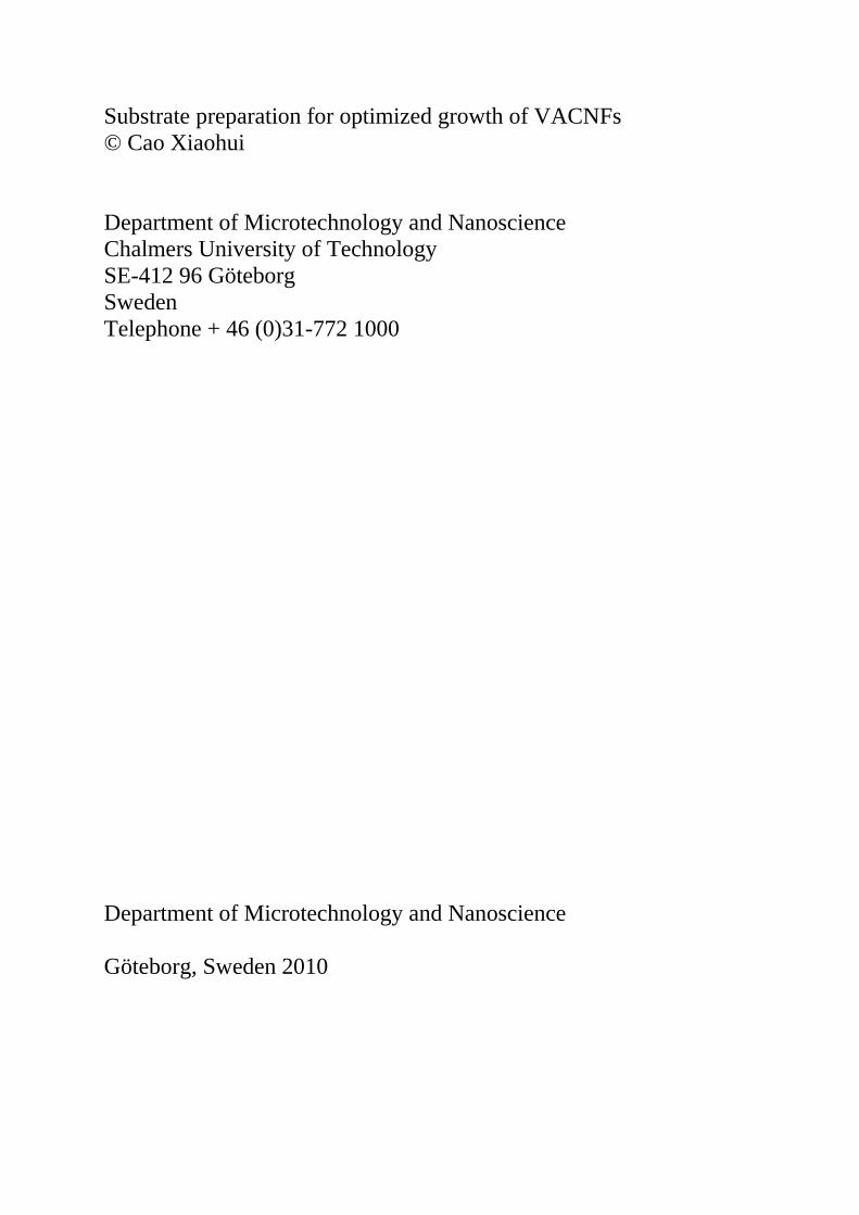
Since the first report in 1991,35 CNTs have received intense interest worldwide. CNTs could be further divided into SWNTs (single-walled carbon nanotubes) and MWNT (multi-walled carbon nanotubes). A single-wall carbon nanotube could be viewed as a graphite layer rolled up to a pipe. SWNTs are further sorted by the orientation of the lattice with respect to the tube axis, that is, how the graphite is rolled up.14 The axis orientation is denoted as chirality, which is defined in terms of a chiral vector, see figure 1:
, There are two specified cases for the chirality. When n=m, the structure is called ‘armchair’, When n=0 or m=0, the structure is called ‘zigzag’. The electrical structure of the CNT is very sensitive to its chirality. ‘Armchair’ exhibit very good metallic property, while all other CNT are semiconducting. Especially, if ×=− 3nm integer, these types of carbon nanotubes are small gap semiconductors (band gap ~ 10 meV).15 What is more, carbon nanotubes exhibit high Young’s modulus up to 1 TPa normally, while the typical Young’s modulus of stainless steel is 0.2 TPa.16 In spite of fascinating physical properties, there is still a long way to go to introduce carbon nanotubes into electronic industry due to reasons mentioned in the introduction.
Fig.1 (a) graphene sheet roll-up to SWNT. (b) chirality of CNT. Adopted with permission from Ref. 14
Page 3 of 40
1.3 Carbon nanofiber 1.3.1 Introduction
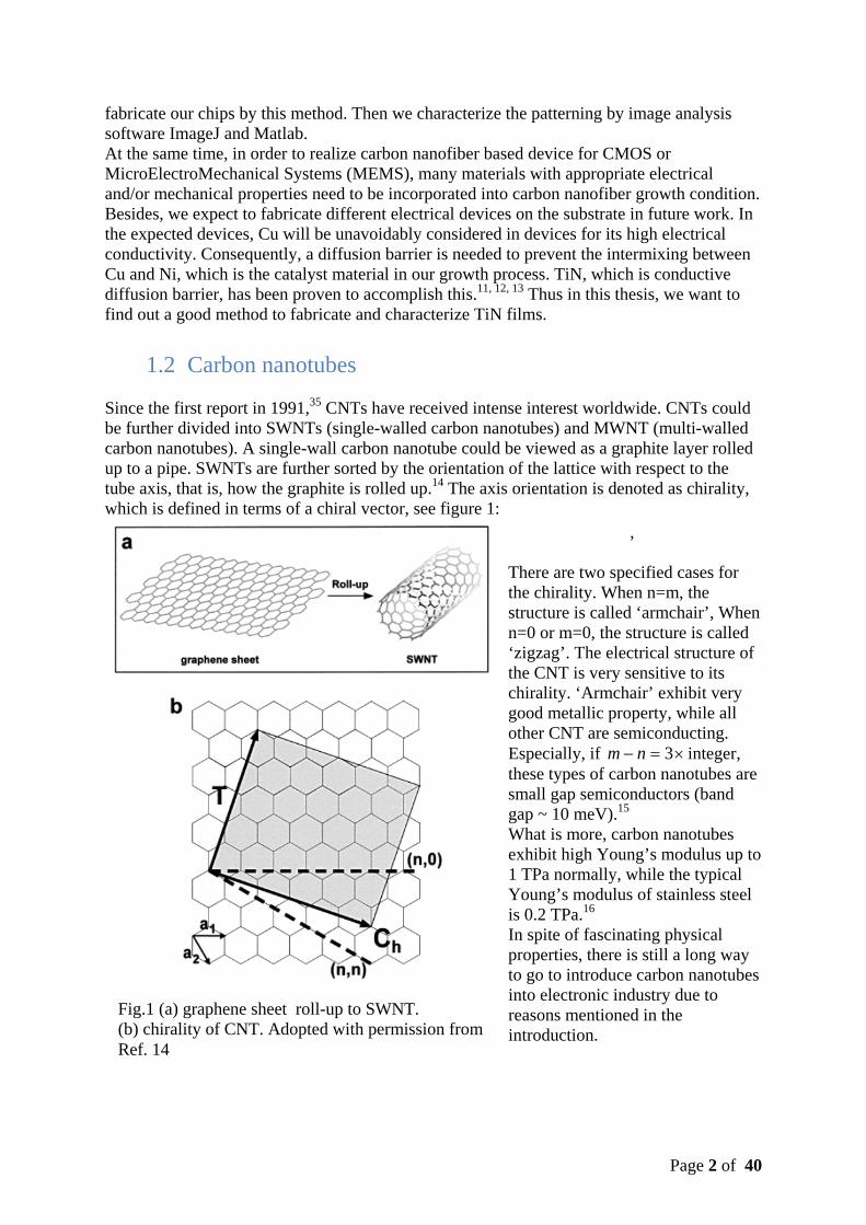
Unlike carbon nanotubes, there is no clear definition of the physical structures of carbon nanofibers. Generally, carbon nanofibers are piled up by conical graphene layers. See figure 2. Let α denote the angle between the fiber axis and the graphene plane. When α is equal to zero, it is carbon nanotube obviously.17 For a carbon nanofiber, α has nonzero value and varies according to experimental setups and parameters. It is unlikely for researchers to reach an agreement on the physical and chemical properties of CNFs with different αs, since the total property is determined by ‘in-plane’ and ‘interplane’ components altogether with different weights.
A straight carbon nanofiber grown perpendicular to the substrate is said to be vertically aligned. VACNFs are of special concern, because individual growth is achievable.18, 19 In synthesis, we can aim to control the CNFs’ location, shape, and internal structure to meet different needs, all of which contribute to CNFs’ advantage in ‘lab-on-chip’ systems. So far, many attempts are performed to incorporate CNFs into scientific applications as sensors, probes and emission sources.18-22 The most popular topic is biomedical application of CNF-based systems.23
Fig.2 (a) Single layer of graphene. (b) Cone-structure carbon nanofiber. (c) Carbon nanotube. Adopted with permission from Ref. 17
Page 4 of 40
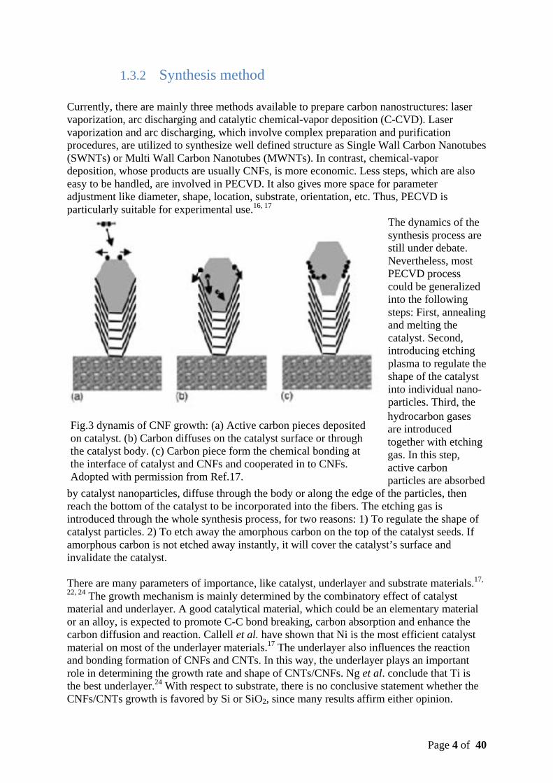
1.3.2 Synthesis method
Currently, there are mainly three methods available to prepare carbon nanostructures: laser vaporization, arc discharging and catalytic chemical-vapor deposition (C-CVD). Laser vaporization and arc discharging, which involve complex preparation and purification procedures, are utilized to synthesize well defined structure as Single Wall Carbon Nanotubes (SWNTs) or Multi Wall Carbon Nanotubes (MWNTs). In contrast, chemical-vapor deposition, whose products are usually CNFs, is more economic. Less steps, which are also easy to be handled, are involved in PECVD. It also gives more space for parameter adjustment like diameter, shape, location, substrate, orientation, etc. Thus, PECVD is particularly suitable for experimental use.16, 17
The dynamics of the synthesis process are still under debate. Nevertheless, most PECVD process could be generalized into the following steps: First, annealing and melting the catalyst. Second, introducing etching plasma to regulate the shape of the catalyst into individual nano-particles. Third, the hydrocarbon gases are introduced together with etching gas. In this step, active carbon particles are absorbed
by catalyst nanoparticles, diffuse through the body or along the edge of the particles, then reach the bottom of the catalyst to be incorporated into the fibers. The etching gas is introduced through the whole synthesis process, for two reasons: 1) To regulate the shape of catalyst particles. 2) To etch away the amorphous carbon on the top of the catalyst seeds. If amorphous carbon is not etched away instantly, it will cover the catalyst’s surface and invalidate the catalyst. There are many parameters of importance, like catalyst, underlayer and substrate materials.17,
22, 24 The growth mechanism is mainly determined by the combinatory effect of catalyst material and underlayer. A good catalytical material, which could be an elementary material or an alloy, is expected to promote C-C bond breaking, carbon absorption and enhance the carbon diffusion and reaction. Callell et al. have shown that Ni is the most efficient catalyst material on most of the underlayer materials.17 The underlayer also influences the reaction and bonding formation of CNFs and CNTs. In this way, the underlayer plays an important role in determining the growth rate and shape of CNTs/CNFs. Ng et al. conclude that Ti is the best underlayer.24 With respect to substrate, there is no conclusive statement whether the CNFs/CNTs growth is favored by Si or SiO2, since many results affirm either opinion.
Fig.3 dynamis of CNF growth: (a) Active carbon pieces deposited on catalyst. (b) Carbon diffuses on the catalyst surface or through the catalyst body. (c) Carbon piece form the chemical bonding at the interface of catalyst and CNFs and cooperated in to CNFs. Adopted with permission from Ref.17.

Page 5 of 40
In our trials, we want to grow CNFs on SiO2/TiN/Ni. The main problem to grow CNFs/CNTs on patterned metal on a SiO2 substrate is the electrical breakdown through the chips. The cause to this problem might be that the charge cannot release instantly on SiO2 surface, which leads a local high voltage. A common solution is to apply a continuous metal layer like Cr or TiN, which will be eliminated latter, to make the whole chip electrically conductive. Nevertheless, we prefer an optimal growth condition under which CNFs growth will occur on the chips with large areas of bare SiO2, to avoid extra processing after the CNFs growth, which may harm the CNFs. Concerning the TiN film, good results have been achieved to grow CNTs on continuous TiN film.11, 25 However, there are no reported results about CNF gowth on patterned TiN on top of an insulating substrate.
Page 6 of 40
2. Hole-mask colloidal lithography
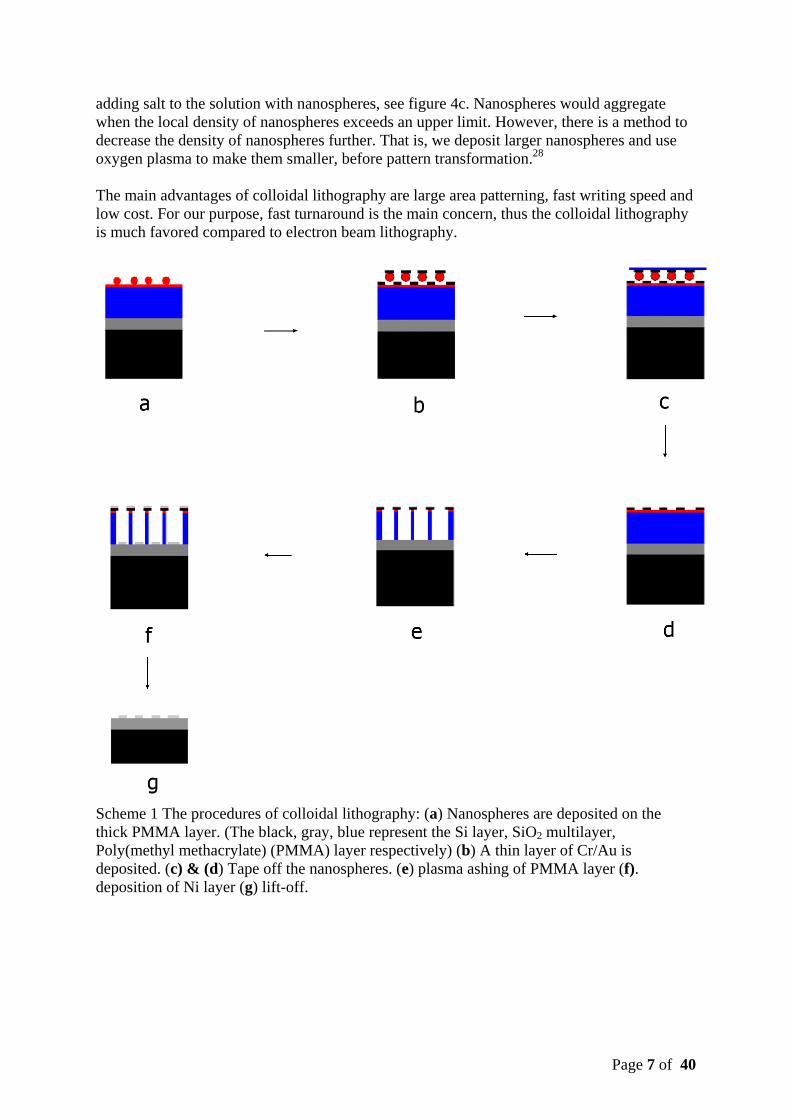
2.1 Colloidal lithography Colloidal lithography (CL) is a novel nanofabrication method which has been explored to build various 2D or 3D templates.26 After several years’ development, CL has evolved into many branches. The common feature shared by all kinds of CL is that they utilize nanospheres to build the mask of patterning. In original CL, the nanospheres are densely arranged on the surface of the substrate and form a self-assembled monolayer. The resulting pattern will form by the material depositing through the apertures between the spheres. The final patterns mostly show a hexagonal symmetry. However, a perfect dense array of particles, which is not required in some cases, is hard to achieve. Therefore, sparse colloidal lithography is proposed in which the nanospheres are sparely distributed. In sparse colloidal lithography (SCL) method, the patterns of nanospheres are directly written on the substrate by etching or evaporation. As an etching mask, the nanospheres are deposited directly on the material to be patterned. After etching , nanodisks will form. Nano-holes will be obtained, if the nanospheres are distributed on the substrate before evaporation of the material to be patterned.27 In spite of its convenience, the limitations of SCL are significant. SCL does not work where the etching rate of the material to be patterned is comparable with the etching rate of the nanospheres and of the substrate. Some materials are not favored either, if their functionalities are sensitive to the etching process. As an improved method, hole-mask colloidal lithography (HCL) brings in more options with regards to materials. The essential difference is that an additional polymeric layer is added below the nanospheres. Then a thin film is deposited. After the spheres are removed by adhesive tape, the thin film with nanoholes is left. If further treated with oxygen plasma, the polymeric layer will be consumed to form a nice undercut which is good for an ensuing lift-off process. See Scheme.1, which gives an illustration of the HCL process. A PMMA layer is span on the substrate as a sacrificing layer and subsequently etched by the oxygen plasma to make PMMA surface more hydrophilic. Then the PDDA solvent is dripped on the substrate and a thin PDDA layer with negative charge is formed on the surface. Then nanospheres solvent is dripped on the substrate. The nanospheres are positively charged, thus they will move towards and attach to the PDDA surface due to the electrostatic force between the nanosphers and the PDDA layer. The patterns of nanopheres on PDDA layer show a typical distance between the most neighboring nanospheres which is cause by the electrostatic repelling force between them. Afterward, a thin Cr/Au layer is evaporated on the top and nanospheres are got rid of by the tape or ultrasonic. The hole mask is formed consequently. The holes are the same size with the nanospheres. Oxygen plasma is carried out again to consume the PMMA layer and develop a good undercut for the succeeding evaporation. In all, the hole-mask technique significantly increases the versatility of colloidal lithography. The patterning of colloidal lithography is highly restricted. The sizes of particles are mainly determined by the size of nanospheres. The patterns are randomly distributed with a limited short-range ordering which is shown by a typical distance between the neighboring nanospheres. The minimum density of particles is determined by the maximum spacing between neighboring nanospheres which in turn is decided by the electrostatic force between particles. For convenience, we call it ‘pair distance’. The pair distance could be shortened by
Page 7 of 40
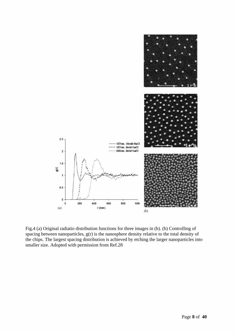
adding salt to the solution with nanospheres, see figure 4c. Nanospheres would aggregate when the local density of nanospheres exceeds an upper limit. However, there is a method to decrease the density of nanospheres further. That is, we deposit larger nanospheres and use oxygen plasma to make them smaller, before pattern transformation.28 The main advantages of colloidal lithography are large area patterning, fast writing speed and low cost. For our purpose, fast turnaround is the main concern, thus the colloidal lithography is much favored compared to electron beam lithography.
Scheme 1 The procedures of colloidal lithography: (a) Nanospheres are deposited on the thick PMMA layer. (The black, gray, blue represent the Si layer, SiO2 multilayer, Poly(methyl methacrylate) (PMMA) layer respectively) (b) A thin layer of Cr/Au is deposited. (c) & (d) Tape off the nanospheres. (e) plasma ashing of PMMA layer (f). deposition of Ni layer (g) lift-off.
Page 8 of 40
Fig.4 (a) Original radiatio distribution functions for three images in (b). (b) Controlling of spacing between nanoparticles, g(r) is the nanosphere density relative to the total density of the chips. The largest spacing distribution is achieved by etching the larger nanoparticles into smaller size. Adopted with permission from Ref.28
Page 9 of 40
2.2 Improved radial distribution function
2.2.1 Orginial function It is an open question whether the spacing of the catalyst seeds will affect the growth of CNFs or not. Still it is rather nice if we could judge the pair distribution for deposited patterns. Originally, we use radial distribution function proposed by J.Sjollema and H.J. Busscher.29 The radial pair distribution function is subsequently defined by:
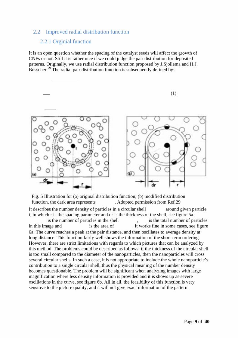
It describes the number density of particles in a circular shell around given particle i, in which r is the spacing parameter and dr is the thickness of the shell, see figure.5a.
is the number of particles in the shell , is the total number of particles in this image and is the area of . It works fine in some cases, see figure 6a. The curve reaches a peak at the pair distance, and then oscillates to average density at long distance. This function fairly well shows the information of the short-term ordering. However, there are strict limitations with regards to which pictures that can be analyzed by this method. The problems could be described as follows: if the thickness of the circular shell is too small compared to the diameter of the nanoparticles, then the nanoparticles will cross several circular shells. In such a case, it is not appropriate to include the whole nanoparticle’s contribution to a single circular shell, thus the physical meaning of the number density becomes questionable. The problem will be significant when analyzing images with large magnification where less density information is provided and it is shows up as severe oscillations in the curve, see figure 6b. All in all, the feasibility of this function is very sensitive to the picture quality, and it will not give exact information of the pattern.
Fig. 5 Illustration for (a) original distribution function; (b) modified distribution function, the dark area represents . Adopted permission from Ref.29
(1)
Page 10 of 40
2.2.2 Modified function
The function we finally use to analyze images is called the radial coverage distribution function, which is defined by:
where takes the place of , representing the sum of the fractional areas enclosed by over all particles, see the shadow area in figure 5b. The resulting curve is smooth, even if the data is limited. What is more, the resolution of the circular shell could be very small and the physical meaning of the function is explicit all the time. Have in mind that the density is normal to average density at long distance. We use absolute density here for later convenience to observe the change in total density.
(2)
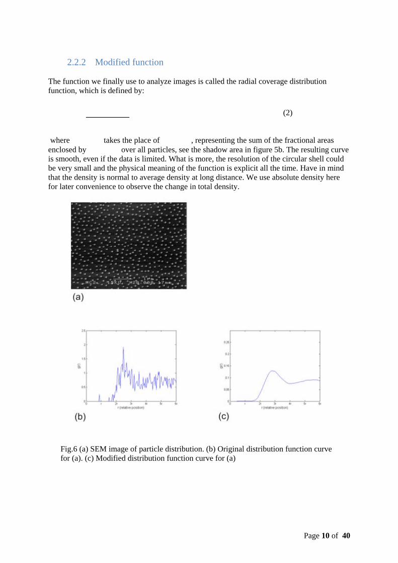
Fig.6 (a) SEM image of particle distribution. (b) Original distribution function curve for (a). (c) Modified distribution function curve for (a)
Page 11 of 40
2.3 Experiments and surface morphology characterization
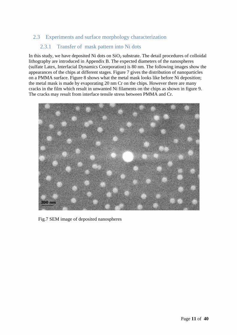
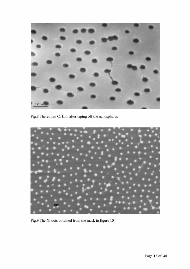
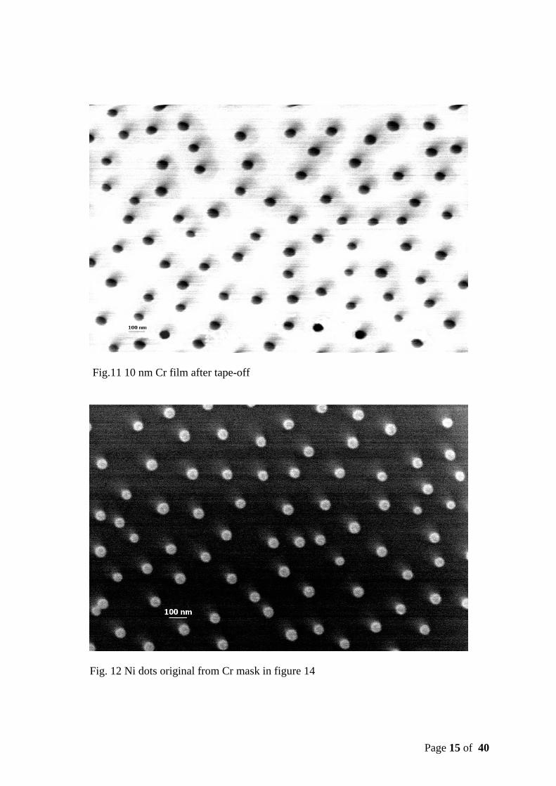
2.3.1 Transfer of mask pattern into Ni dots In this study, we have deposited Ni dots on SiO2 substrate. The detail procedures of colloidal lithography are introduced in Appendix B. The expected diameters of the nanospheres (sulfate Latex, Interfacial Dynamics Coorporation) is 80 nm. The following images show the appearances of the chips at different stages. Figure 7 gives the distribution of nanoparticles on a PMMA surface. Figure 8 shows what the metal mask looks like before Ni deposition; the metal mask is made by evaporating 20 nm Cr on the chips. However there are many cracks in the film which result in unwanted Ni filaments on the chips as shown in figure 9. The cracks may result from interface tensile stress between PMMA and Cr.
Fig.7 SEM image of deposited nanospheres
Page 12 of 40
Fig.8 The 20 nm Cr film after taping off the nanospheres
Fig.9 The Ni dots obtained from the mask in figure 10
Page 13 of 40
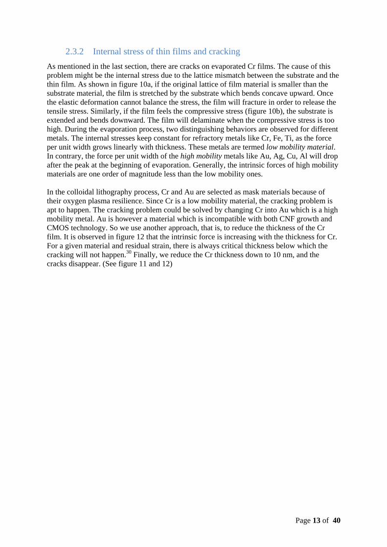
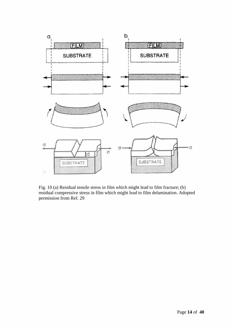
2.3.2 Internal stress of thin films and cracking As mentioned in the last section, there are cracks on evaporated Cr films. The cause of this problem might be the internal stress due to the lattice mismatch between the substrate and the thin film. As shown in figure 10a, if the original lattice of film material is smaller than the substrate material, the film is stretched by the substrate which bends concave upward. Once the elastic deformation cannot balance the stress, the film will fracture in order to release the tensile stress. Similarly, if the film feels the compressive stress (figure 10b), the substrate is extended and bends downward. The film will delaminate when the compressive stress is too high. During the evaporation process, two distinguishing behaviors are observed for different metals. The internal stresses keep constant for refractory metals like Cr, Fe, Ti, as the force per unit width grows linearly with thickness. These metals are termed low mobility material. In contrary, the force per unit width of the high mobility metals like Au, Ag, Cu, Al will drop after the peak at the beginning of evaporation. Generally, the intrinsic forces of high mobility materials are one order of magnitude less than the low mobility ones. In the colloidal lithography process, Cr and Au are selected as mask materials because of their oxygen plasma resilience. Since Cr is a low mobility material, the cracking problem is apt to happen. The cracking problem could be solved by changing Cr into Au which is a high mobility metal. Au is however a material which is incompatible with both CNF growth and CMOS technology. So we use another approach, that is, to reduce the thickness of the Cr film. It is observed in figure 12 that the intrinsic force is increasing with the thickness for Cr. For a given material and residual strain, there is always critical thickness below which the cracking will not happen.30 Finally, we reduce the Cr thickness down to 10 nm, and the cracks disappear. (See figure 11 and 12)
Page 14 of 40
Fig. 10 (a) Residual tensile stress in film which might lead to film fracture; (b) residual compressive stress in film which might lead to film delamination. Adopted permission from Ref. 29
Page 15 of 40
Fig.11 10 nm Cr film after tape-off
Fig. 12 Ni dots original from Cr mask in figure 14
Page 16 of 40
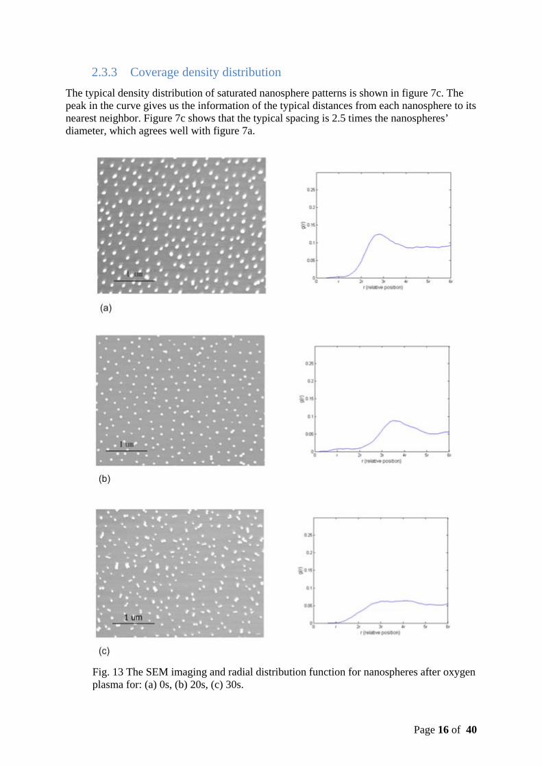
2.3.3 Coverage density distribution The typical density distribution of saturated nanosphere patterns is shown in figure 7c. The peak in the curve gives us the information of the typical distances from each nanosphere to its nearest neighbor. Figure 7c shows that the typical spacing is 2.5 times the nanospheres’ diameter, which agrees well with figure 7a.
Fig. 13 The SEM imaging and radial distribution function for nanospheres after oxygen plasma for: (a) 0s, (b) 20s, (c) 30s.

Page 17 of 40
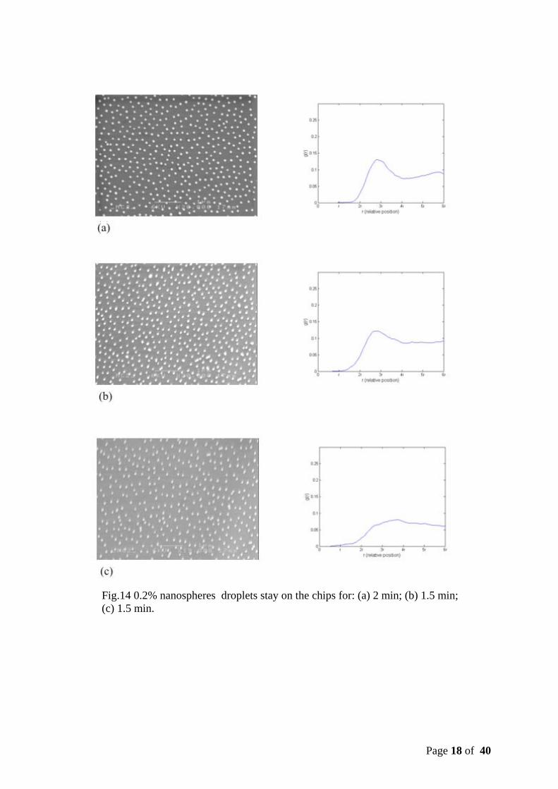
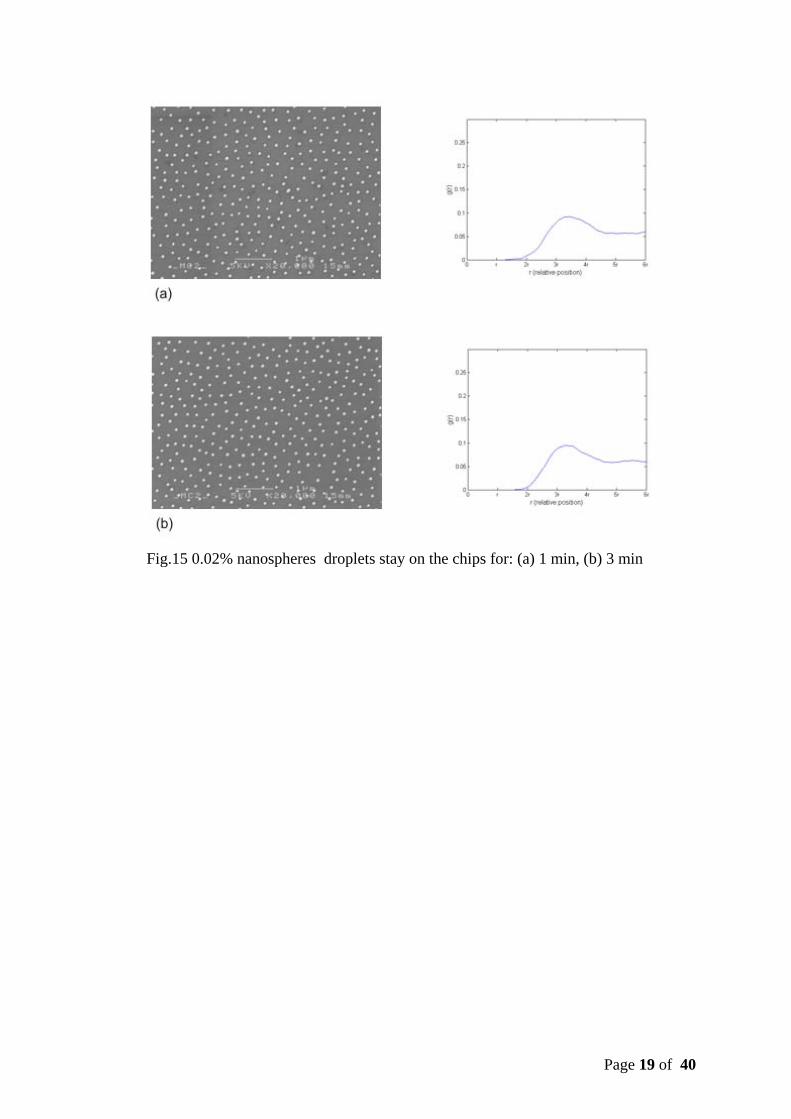
In order to have more control over the colloidal patterns, we apply the oxygen plasma to 80 nm nanospheres and the resulting patterns are shown in figure 13. The 20 s oxygen plasma etching (figure 13b) shrinks the nanospheres’ sizes down to about 60 nm while the short term ordering of nanospheres is well kept. Since the absolute distances between the centers of the mass stand still, the peak of the curve, relative to the nanoparticle diameter, is shifted. However, the oxygen plasma will reach its limit when the etching time approaches 30 s. Both the uniformity and the ordering of the nanospheres are destroyed. The reason may be: (1) the isotropy of etching rate are no longer good enough compared to the size of nanospheres. (2) The oxygen plasma etch the PDDA layer as well, while long time etching will consume the PDDA layer so serious that it will disturb the detachment of nanospheres to the PDDA and cause the disordering of nanospheres. We also do some trials to shorten the period the nanospheres droplet stay on the chips. If we use 0.2% nanosphere solvent, both the relative peak height and the average density of chips are lowered when the immersing time is shortened. See figure 14, the relative peak height in figure 14(b) is obviously lower than 14(a). When the immersing time is down to 1 min, the peak nearly vanishes and the overall average density is decreased significantly. However, the nanospheres distribution is relatively stable when we dilute the nanosphere solvent down to 0.02%, see figure 15, and the overall density is significantly lower than those before solvent is diluted. Based these phenomena, we make following speculations: 1) the uplimit overall average density is determined by the solvent density. 2) Given enough time, Short-term order could be achieved by the pattern modification due to electrostatic force, even if the average density is low. Then we could see that for 0.02% solvent, the pattern quickly reaches its equilibrium patterns. After 1min, the nanospheres deposition is almost finished. For 0.2%, after immersing in solvent for 1min, the overall density hasn’t saturated. For 1min and half, the nanospheres are still on their way to re-organize their positions. Based on these experiments, I propose to further dilute the solvent. In this way, we might expect a pattern that there are dot pairs distributed on the chips where pair distance show typical value and pair-pair distance is sufficiently large. On these kinds of chips, it is possible to observe pair-growth of CNFs.
Page 18 of 40
Fig.14 0.2% nanospheres droplets stay on the chips for: (a) 2 min; (b) 1.5 min;
(c) 1.5 min.
Page 19 of 40
Fig.15 0.02% nanospheres droplets stay on the chips for: (a) 1 min, (b) 3 min
Page 20 of 40
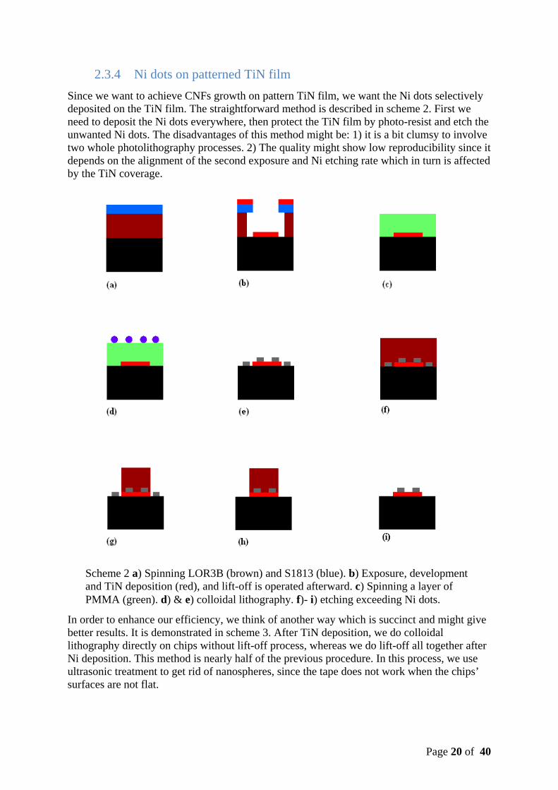
2.3.4 Ni dots on patterned TiN film Since we want to achieve CNFs growth on pattern TiN film, we want the Ni dots selectively deposited on the TiN film. The straightforward method is described in scheme 2. First we need to deposit the Ni dots everywhere, then protect the TiN film by photo-resist and etch the unwanted Ni dots. The disadvantages of this method might be: 1) it is a bit clumsy to involve two whole photolithography processes. 2) The quality might show low reproducibility since it depends on the alignment of the second exposure and Ni etching rate which in turn is affected by the TiN coverage.
In order to enhance our efficiency, we think of another way which is succinct and might give better results. It is demonstrated in scheme 3. After TiN deposition, we do colloidal lithography directly on chips without lift-off process, whereas we do lift-off all together after Ni deposition. This method is nearly half of the previous procedure. In this process, we use ultrasonic treatment to get rid of nanospheres, since the tape does not work when the chips’ surfaces are not flat.
Scheme 2 a) Spinning LOR3B (brown) and S1813 (blue). b) Exposure, development and TiN deposition (red), and lift-off is operated afterward. c) Spinning a layer of PMMA (green). d) & e) colloidal lithography. f)- i) etching exceeding Ni dots.
Page 21 of 40
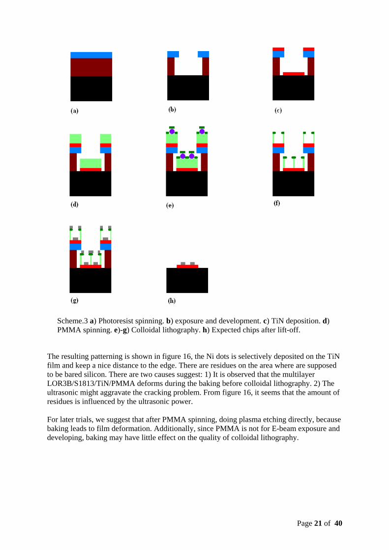
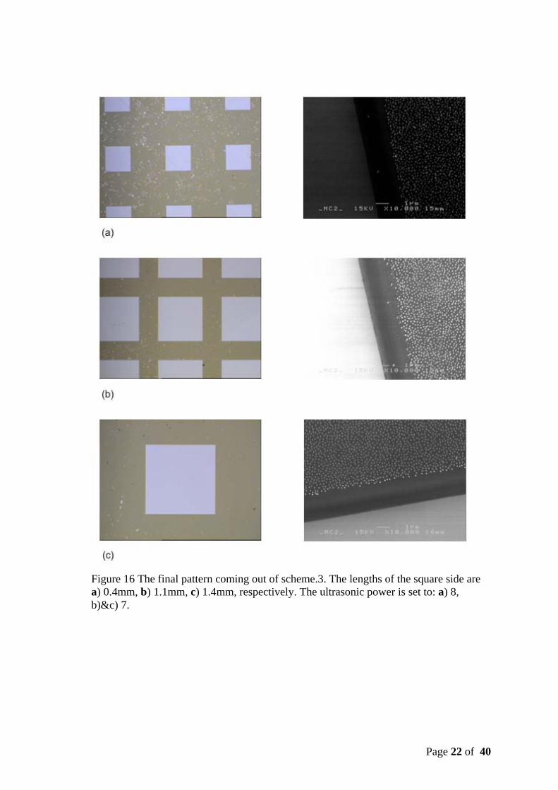
The resulting patterning is shown in figure 16, the Ni dots is selectively deposited on the TiN film and keep a nice distance to the edge. There are residues on the area where are supposed to be bared silicon. There are two causes suggest: 1) It is observed that the multilayer LOR3B/S1813/TiN/PMMA deforms during the baking before colloidal lithography. 2) The ultrasonic might aggravate the cracking problem. From figure 16, it seems that the amount of residues is influenced by the ultrasonic power. For later trials, we suggest that after PMMA spinning, doing plasma etching directly, because baking leads to film deformation. Additionally, since PMMA is not for E-beam exposure and developing, baking may have little effect on the quality of colloidal lithography.
Scheme.3 a) Photoresist spinning. b) exposure and development. c) TiN deposition. d) PMMA spinning. e)-g) Colloidal lithography. h) Expected chips after lift-off.
Page 22 of 40
Figure 16 The final pattern coming out of scheme.3. The lengths of the square side are a) 0.4mm, b) 1.1mm, c) 1.4mm, respectively. The ultrasonic power is set to: a) 8, b)&c) 7.
Page 23 of 40
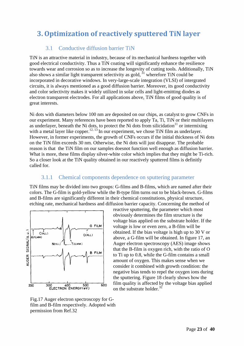
Fig.17 Auger electron spectroscopy for G-film and B-film respectively. Adopted with permission from Ref.32
3. Optimization of reactively sputtered TiN layer
3.1 Conductive diffusion barrier TiN TiN is an attractive material in industry, because of its mechanical hardness together with good electrical conductivity. Thus a TiN coating will significantly enhance the resilience towards wear and corrosion so as to increase the longevity of cutting tools. Additionally, TiN also shows a similar light transparent selectivity as gold, 31 wherefore TiN could be incorporated in decorative windows. In very-large-scale integration (VLSI) of intergrated circuits, it is always mentioned as a good diffusion barrier. Moreover, its good conductivity and color selectivity makes it widely utilized in solar cells and light-emitting diodes as electron transparent electrodes. For all applications above, TiN films of good quality is of great interests. Ni dots with diameters below 100 nm are deposited on our chips, as catalyst to grow CNFs in our experiment. Many references have been reported to apply Ta, Ti, TiN or their multilayers as underlayer, beneath the Ni dots, to protect the Ni dots from silicidation11 or intermixing with a metal layer like copper.12, 13 In our experiment, we chose TiN film as underlayer. However, in former experiments, the growth of CNFs occurs if the initial thickness of Ni dots on the TiN film exceeds 30 nm. Otherwise, the Ni dots will just disappear. The probable reason is that the TiN film on our samples doesnot function well enough as diffusion barrier. What is more, these films display silver-white color which implies that they might be Ti-rich. So a closer look at the TiN quality obtained in our reactively sputtered films is definitly called for.
3.1.1 Chemical components dependence on sputtering parameter TiN films may be divided into two groups: G-films and B-films, which are named after their colors. The G-film is gold-yellow while the B-type film turns out to be black-brown. G-films and B-films are significantly different in their chemical constitutions, physical structure, etching rate, mechanical hardness and diffusion barrier capacity. Concerning the method of
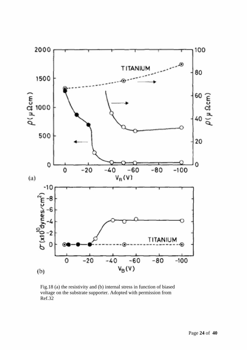
reactive sputtering, the parameter which most obviously determines the film structure is the voltage bias applied on the substrate holder. If the voltage is low or even zero, a B-film will be obtained. If the bias voltage is high up to 30 V or above, a G-film will be obtained. In figure 17, an Auger electron spectroscopy (AES) image shows that the B-film is oxygen rich, with the ratio of O to Ti up to 0.8, while the G-film contains a small amount of oxygen. This makes sense when we consider it combined with growth condition: the negative bias tends to repel the oxygen ions during the sputtering. Figure 18 clearly shows how the film quality is affected by the voltage bias applied on the substrate holder.32
Page 24 of 40
Fig.18 (a) the resistivity and (b) internal stress in function of biased voltage on the substrate supporter. Adopted with permission from Ref.32
Page 25 of 40
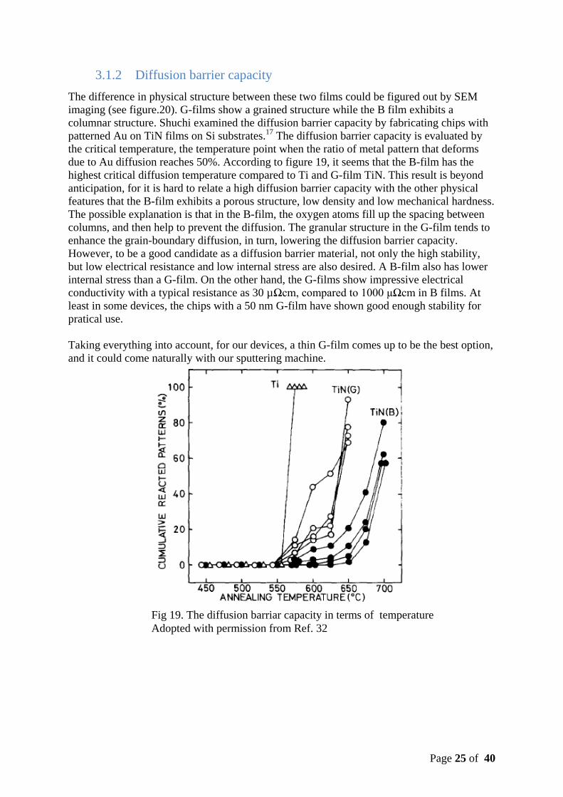
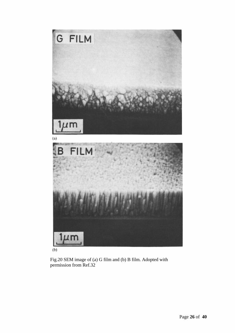
3.1.2 Diffusion barrier capacity The difference in physical structure between these two films could be figured out by SEM imaging (see figure.20). G-films show a grained structure while the B film exhibits a columnar structure. Shuchi examined the diffusion barrier capacity by fabricating chips with patterned Au on TiN films on Si substrates.17 The diffusion barrier capacity is evaluated by the critical temperature, the temperature point when the ratio of metal pattern that deforms due to Au diffusion reaches 50%. According to figure 19, it seems that the B-film has the highest critical diffusion temperature compared to Ti and G-film TiN. This result is beyond anticipation, for it is hard to relate a high diffusion barrier capacity with the other physical features that the B-film exhibits a porous structure, low density and low mechanical hardness. The possible explanation is that in the B-film, the oxygen atoms fill up the spacing between columns, and then help to prevent the diffusion. The granular structure in the G-film tends to enhance the grain-boundary diffusion, in turn, lowering the diffusion barrier capacity. However, to be a good candidate as a diffusion barrier material, not only the high stability, but low electrical resistance and low internal stress are also desired. A B-film also has lower internal stress than a G-film. On the other hand, the G-films show impressive electrical conductivity with a typical resistance as 30 µΩcm, compared to 1000 µΩcm in B films. At least in some devices, the chips with a 50 nm G-film have shown good enough stability for pratical use. Taking everything into account, for our devices, a thin G-film comes up to be the best option, and it could come naturally with our sputtering machine.
Fig 19. The diffusion barriar capacity in terms of temperature Adopted with permission from Ref. 32
Page 26 of 40
Fig.20 SEM image of (a) G film and (b) B film. Adopted with permission from Ref.32
Page 27 of 40
3.2 Thin film analysis methods There are many options to identify the quality of the TiN film that we obtain on our chips. We could just judge film type from color. In order to observe the microstructure, we could exam the film by SEM. To further identify the chemical status of the film, Auger electron spectroscopy (AES), X-ray photoelectron spectroscopy (XPS), Rutherford backscattering spectrometry (RBS) are most frequently used. The features of these methods are summerised in table I.
Technique Incident beam Signal
Information Lateral resolution Depth Bonding
Analysis Element Quantity Analyse
XPS Photon Electron Surface Easy All
expect H, He
Sub quantitative bad
AES Electron Electron monolayer hard All
expect H, He
Sub quantitative Good
RBS Ion Ion Deep information hard All quantitative Very
good Although the signals of XPS and AES do not carry information from deep inside the sample, they could give a depth profile if combined with Ar ion beam sputtering. For our purpose, we judge the film type by looking at the color and identifying the physical structure by SEM. Then we measure the resistivity of TiN films
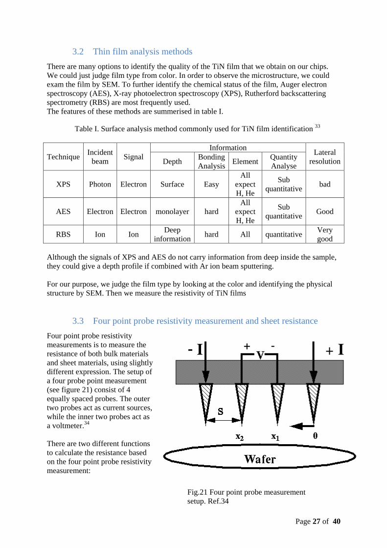
3.3 Four point probe resistivity measurement and sheet resistance Four point probe resistivity measurements is to measure the resistance of both bulk materials and sheet materials, using slightly different expression. The setup of a four probe point measurement (see figure 21) consist of 4 equally spaced probes. The outer two probes act as current sources, while the inner two probes act as a voltmeter.34 There are two different functions to calculate the resistance based on the four point probe resistivity measurement:
Table I. Surface analysis method commonly used for TiN film identification 33
Fig.21 Four point probe measurement setup. Ref.34

Page 28 of 40
(3)
(4)
(7)
Bulk material:
The differential expression of resistance is: AXR ∆
=∆ρ
When the thickness t >> probe spacing s, the cross-section of the current could be viewed as a hemisphere surface. The total resistance is the intergration between two probes:
- The net current is the superposition of current from two outer tips, thus the Ohm law expression for four-point measure is:
We arrive at the bulk resistivity expression:
Thin film: When the t << s, the cross-section of current flow becomes ring instead of spheres: For
(5)
(6)
Page 29 of 40
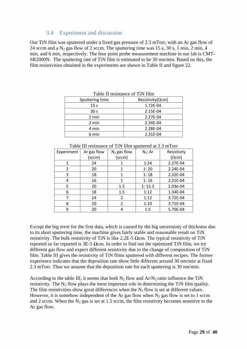
3.4 Experiment and discussion Our TiN film was sputtered under a fixed gas pressure of 2.3 mTorr, with an Ar gas flow of 24 sccm and a N2 gas flow of 2 sccm. The sputtering time was 15 s, 30 s, 1 min, 2 min, 4 min, and 6 min, respectively. The four point probe measurement machine in our lab is CMT-SR2000N. The sputtering rate of TiN film is estimated to be 30 nm/min. Based on this, the film resistivities obtained in the experiments are shown in Table II and figure 22.
Table II resistance of TiN film Sputtering time Resistivity(Ωcm)
15 s 1.72E-04 30 s 2.15E-04
1 min 2.27E-04 2 min 2.34E-04 4 min 2.28E-04 6 min 2.31E-04
Table III resistance of TiN film sputtered at 2.3 mTorr
Experiment Ar gas flow (sccm)
N2 gas flow (sccm)
N2: Ar Resistivity (Ωcm)
1 24 1 1:24 2.27E-04 2 20 1 1: 20 2.24E-04 3 18 1 1: 18 2.32E-04 4 16 1 1: 16 2.21E-04 5 20 1.5 1: 13.3 2.03e-04 6 18 1.5 1:12 1.34E-04 7 24 2 1:12 3.72E-04 8 20 2 1:10 3.71E-04 9 20 4 1:5 5.70E-04
Except the big error for the first data, which is caused by the big uncertainty of thickness due to its short sputtering time, the machine gives fairly stable and reasonable result on TiN resistivity. The bulk resistivity of TiN is like 2.2E-5 Ωcm. The typical resistivity of TiN reported so far reported is 3E-5 Ωcm. In order to find out the optimized TiN film, we try different gas flow and expect different resistivity due to the change of composition of TiN film. Table III gives the resistivity of TiN films sputtered with different recipes. The former experience indicates that the deposition rate show little different around 30 nm/min at fixed 2.3 mTorr. Thus we assume that the deposition rate for each sputtering is 30 nm/min. According to the table III, it seems that both N2 flow and Ar/N2 ratio influence the TiN resistivity. The N2 flow plays the most important role in determining the TiN film quality. The film resistivities show great differences when the N2 flow is set at different values. However, it is somehow independent of the Ar gas flow when N2 gas flow is set to 1 sccm and 2 sccm. When the N2 gas is set at 1.5 sccm, the film resistivity becomes sensitive to the Ar gas flow.
Page 30 of 40
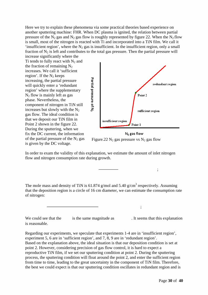
Here we try to explain these phenomena via some practical theories based experience on another sputtering machine: FHR. When DC plasma is ignited, the relation between partial pressure of the N2 gas and N2 gas flow is roughly represented by figure 22. When the N2 flow is small, most of the nitrogen is reacted with Ti and incorporated into a TiN film. We call it ‘insufficient region’, where the N2 gas is insufficient. In the insufficient region, only a small fraction of N2 is left and contributes to the total gas pressure. Then the partial pressure will increase significantly where the Ti tends to fully react with N2 and the fraction of remaining N2 increases. We call it ‘sufficient region’. If the N2 keeps increasing, the partial pressure will quickly enter a ‘redundant region’ where the supplementary N2 flow is mainly left as gas phase. Nevertheless, the component of nitrogen in TiN still increases but slowly with the N2 gas flow. The ideal condition is that we deposit our TiN film in Point 2 shown in the figure 22. During the sputtering, when we fix the DC current, the information of the partial pressure of the N2 gas is given by the DC voltage. In order to exam the validity of this explanation, we estimate the amount of inlet nitrogen flow and nitrogen consumption rate during growth.
; The mole mass and density of TiN is 61.874 g/mol and 5.40 g/cm3 respectively. Assuming that the deposition region is a circle of 16 cm diameter, we can estimate the consumption rate of nitrogen:
; We could see that the is the same magnitude as . It seems that this explanation is reasonable. Regarding our experiments, we speculate that experiments 1-4 are in ‘insufficient region’, experiment 5, 6 are in ‘sufficient region’, and 7, 8, 9 are in ‘redundant region’. Based on the explanation above, the ideal situation is that our deposition condition is set at point 2. However, considering precision of gas flow control, it is hard to expect a reproductive TiN film, if we set our sputtering condition at point 2. During the sputtering process, the sputtering condition will float around the point 2, and enter the sufficient region from time to time, leading to the great uncertainty in the component of TiN film. Therefore, the best we could expect is that our sputtering condition oscillates in redundant region and is
Figure.22 N2 gas pressure vs N2 gas flow

Page 31 of 40
as close as possible to the point 2. For further trials, we suggest that to find an optimized sputtering condition, it is better to set N2 flow at 1.5 sccm and adjust the Ar flow, paying attention to the DC voltage during each process.

Page 32 of 40
4. Conclusion In this thesis, we successfully realize mass fabrication of Ni nanodiscs by hole-mask colloidal lithography on wafer scale. The patterning is uniform and reproducible. Then we find an improved method to characterize the ordering of the discs, and the short scale ordering is observed in the graph. Further, we realize some control over Ni dots’ patterns and distribution. Additionally, we have roughly found out how the quality of TiN films is influenced by gas flow during the sputtering.

Page 33 of 40
Acknowledgment: I would like to express my sincere gratitude to everyone who helped me in this thesis project. I am really grateful to my Per Lundgen. Thanks for allowing me to do my master thesis in your research group, where I really learned a lot and experienced a happy time and had a lot of fun. Thanks for your guidance, suggestion and encouragement, always. Thanks to Farzan Alavian Ghavanini for giving his inspiring idea and sharing his precious practical experience during my thesis work Hans Fredriksson, thanks for your kind, patient, explicit teaching on colloidal lithography and SEM. Henrik Frederiksen, thanks for your always kind, instant help on deposition machine and inspiring discussion on TiN sputtering. Yifeng Fu, Teng Wang, Sun Jie, thanks for your valuable suggestions and help in the lab during this period. Special Thanks to my old friends and new friends who show up during these two years. Your companies light me up during my stay in Gothenburg. I will forever treasure this period all my life.
Page 34 of 40
Reference: 1 IBM J. Res. Dev., Vol. 46, No. 2/3(2002) 2 K. Osada, Y. Saitoh, E. Ibe, and K. Ishibashi, A cell tunnel-leakage-suppressed 16 Mb SRAM for handling cosmic-ray-induced multi-errors. Session 17.2, International Solid-State Conference, 2003. 3 A. K. Geim, and K. S. Novoselov, The Rise of Graphene. Nature Materials, 6, 183(2007) 4 Adrian Bachtold, et al, Logic Circuits with Carbon Nanotube Transistors. Science 294, 1317 (2001); 5 Ali Javey, Ballistic carbon nanotube field-effect transistors. Nature, 424, 654 (2003) 6 J. Tersoff, Contact resistance of carbon nanotubes. Appl. Phys. Lett. 74, 15, 2122(1999) 7 A. Bachtold, M. Henny, C. Terrier, C. Strunk, and C. Schönenberger, Contacting carbon
nanotubes selectively with low-ohmic contacts for four-probe electric measurements. Appl. Phys. Lett. 73, 2, 274(1998) 8 McKnight T E, Melechko A V, Austin D W, Sims T, Guillorn M A and Simpson M L, Microarrays of Vertically-Aligned Carbon Nanofiber Electrodes in an Open Fluidic Channel. J. Phys. Chem. B, 108, 22, 7115(2004) 9 Nguyen-Vu T D B, Chen H, Cassell A M, Andrews R J,Meyyappan M and Li J, Vertically-aligned carbon nanofiber architecture as a multifunctional 3D neural electrical interface. IEEE Trans. Biomed. Eng. 54 1121(2007) 10 Yu Z, McKnight T E, Ericson M N, Melechko A V, Simpson M L and Morrison B, Vertically aligned carbon nanofiber arrays record electrophysiological signals from hippocampal slices. Nano. Lett. 7, 8, 2188(2007) 11 K. B. K. Teo, Characterization of plasma-enhanced chemical vapor deposition carbonnanotubes by Auger electron spectroscopy. J. Vac. Sci. Technol. B 20(1), 116(2002) 12 J Garcia-Cespedes, Optimal deposition conditions of TiN barrier layers for the growth of vertically aligned carbon nanotubes onto metallic substrates. J. Phys. D: Appl. Phys. 42 (2009) 13 Awano. Y, Sato. S, Kondo. D, Ohfuti. M. Kawabata. A, Nihei. M, Yokoyama, N, Carbon nanotube via interconnect technologies: size-classified catalyst nanoparticles and low-resistance ohmic contact formation. Phys. Status Solidi A, 203, 3611(2006). 14 Teri Wang Odom, Jin-Lin Huang, Philip Kim, and Charles M. Lieber, Structure and Electronic Properties of Carbon Nanotubes. J. Phys. Chem. B, 104, 2794-2809(2000) 15 Hongjie Dai. Carbon nanotubes: opportunities and challenges, Surface Science, 500, 218–241(2002) 16 Erik T. Thostenson, Zhifeng Ren, Tsu-Wei Chou. Advances in the science and technology of carbon nanotubes and their composites: a review. Composites Science and Technology, 61, 1899–1912(2001) 17 A. V. Melechko, et al. Vertically aligned carbon nanofibers and related structures: Controlled synthesis and directed assembly. J. App. Phy 97, 041301 (2005) 18 Qi Ye, et al. Large-Scale Fabrications of Carbon Nanotube Probe Tips for Atomic Force Microscopy Critical Dimension Imaging Applications. Nano Letters 4, 7, 1301 (2004) 19 Xiaojing Yang, Michael A. Guillorn, Derek Austin, Anatoli V. Melechko, Hongtao Cui, Harry M. Meyer, Vladimir I. Merkulov, J. B. O. Caughman, Douglas H. Lowndes, and Michael L. Simpson, Fabrication and Characterization of Carbon Nanofiber-Based Vertically Integrated Schottky Barrier Junction Diodes. Nano Lett. 3, 1751(2003) 20 M. A. Guillorn, et al. Operation of a gated field emitter using an individual carbon nanofiber cathode. Appl. Phys. Lett. 79, 3506 (2001) 21 M. A. Guillorn, et at. Individually addressable vertically aligned carbon nanofiber-based electrochemical probes. J. Appl. Phys. 91, 3824 (2002)
Page 35 of 40
22 Alan M Cassell, et al. Combinatorial chips for optimizing the growth and integration of carbon nanofibre based devices. Nanotechnology 15, 9 (2004) 23 Anatoli V Melechko, Ramya Desikan, Timothy E McKnight, Kate L Klein and Philip D Rack, Synthesis of vertically aligned carbon nanofibres for interfacing with live systems. J. Phys. D: Appl. Phys. 42 (2009) 24 H. T. Ng, B. Chen, J. E. Koehne, A. M. Cassell, J. Li, J. Han, and M. Meyyappan, Growth of Carbon Nanotubes: A Combinatorial Method To Study the Effects of Catalysts and Underlayers. J. Phys. Chem. B 107, 8484 (2003). 25
G Pirio, P Legagneux, D Pribat, K B K Teo, M Chhowalla, G A J Amaratunga and W I Milne, Fabrication and electrical characteristics of carbon nanotube field emission microcathodes with an integrated gate electrode. Nanotechnology, 13, 1–4(2002) 26 S.-M.Yang, S. G. Jang,D.-G.Choi, S. Kim, H. K.Yu. Nanomachining by Colloidal Lithography. Small, 2, 458(2006) 27 Hans Fredriksson, Yury Alaverdyan, Alexandre Dmitriev, Christoph Langhammer, Duncan S. Sutherland, Michael Zäch, and Bengt Kasemo, Hole–Mask Colloidal Lithography. Adv. Mater. 19, 4297–4302(2007) 28 Per Hanarp, Duncan S. Sutherland, Julie Gold, Bengt Kasemo. Control of nanoparticle film structure for colloidal lithography. Colloids and Surfaces A: Physicochem. Eng. Aspects 214 (2003) 23-36 29 J.Sjollema and H.J. Busscher, Deposition of Polystyrene Particles in a Parallel Plate Flow Cell. 2. Pair Distribution Functions Between Deposited Particles. Colloids and Surface, 47, 337-352 (1990) 30 Milton Ohring, Materials science of thin films, second section, ELSEVIER 31 Wu-Yih Uen, Zhen-Yu Li, Shan-Ming Lan, Tsun-Neng Yang, San-Mao Liao. Fabrication of low-resistivity and gold-colored TiN films by halide chemical vapor deposition with a low [NH3]/[TiCl4] flow ratio. Thin Solid Films 516 99–103(2007) 32 Shuicui Kanamori, Investigation of reactively sputtered TiN films for diffusion barriers Thin Solid Films. 136, 195-214(1986) 33 Surface analysis methods in materials science D.J. O'Connor, B.A. Sexton, R.St.C. Smart Berlin; New York: Springer-Verlag, cop. 1992 34 Lab manual, UC, Berkeley 35 Sumio Iijima, Helical microtubules of graphitic carbon. Nature, 354, 56(1991)

Page 36 of 40
Appendix A : Code for radical function
%the parameter need to be set: %the data region in XLS file, %diamemer in pixel %Ymax,Xmax contnum=0 A=xlsread('results','F2:G518'); l=length(A) r=16; split=60; resolution=split*7 cont=zeros(resolution+1,2); Ymax=685; Xmax=1021; for n2=2:1:(resolution+1) cont(n2,1)=(n2-1)*r/split; end for n=1:1:l if A(n,1)>7*r&A(n,2)>7*r&A(n,1)<(Xmax-7*r)&A(n,2)<(Ymax-7*r) contnum=contnum+1; for n2=1:1:l if n2~=n if sqrt((A(n2,1)-A(n,1))^2+(A(n2,2)-A(n,2))^2)<6.5*r %if in the big circle R=sqrt((A(n2,1)-A(n,1))^2+(A(n2,2)-A(n,2))^2); for n3=(resolution+1):-1:2 %search for beginning of cutting remain=pi*r^2/4; if (R+r/2)>(n3-1.5)*r/split %find the begining of cutting for n4=n3:-1:2 %cuting loop starts a=(n4-1.5)*r/split; areas=acos(((r/2)^2+R^2-a^2)/2/R/(r/2))/4*r^2; areab=acos((a^2+R^2-(r/2)^2)/2/R/a)*a^2; arealin=a*r/2*sin(acos((a^2+(r/2)^2-R^2)/2/a/(r/2))); cutting=areas+areab-arealin; add=remain-cutting; remain=cutting; cont(n4,2)=cont(n4,2)+add; if (R-r/2)>(n4-2.5)*r/split %break cutting loop cont(n4-1,2)=cont(n4-1,2)+remain; %remaining add break end end %cutting loop ends end if remain~=pi*r^2/4 %break search cutting loop break end end end end end end

Page 37 of 40
end contnum for n2=2:1:resolution C=(pi*(r/split)^2*(2*n2-2)); cont(n2+1,2)=cont(n2+1,2)/C/contnum; end plot(cont(:,1),cont(:,2)) axis([0,6*r,0,0.3]) set(gca,'XTick',0:r:6*r) set(gca,'XTickLabel','0','r','2r','3r','4r','5r','6r')

Page 38 of 40
Appendix B: Colloidal lithography procedures
Resist spinning: Resist name: 950K PMMA A4 Spinning conditions: 4000 rpm, 3000 acc, Expected thickness: 200nm Soft bake: Hotplate 10 minutes @ 170 ˚C Etching Equipment: Plasma Therm Batchtop PE/RIE m/95 Etch: 50W 250mTorr 10sccm, 5 seconds, O2 Colloidal deposition: Elelctrolye: Polydiallyldimethylammonium, MW 200000–350000, Sigma Aldrich Nanoparticles: Sulfate latex, Interfacial Dynamics Coorporation Pippeting electrolyte solvent on chip: 40s Running water: 15s
Blow dry
Pippeting nanoparticles solvent on chip: 3 mins
Rinsed in boiling water: 40s
Running water: 15s
Blow dry
Cr deposition: Equipment: AVAC HVC600 Base pressure: 3.0×10⁻⁶ mbar Pumping –down duration: 1 hour Final thickness: 10 nm Tape-off Tape: SWT-10 tape, Nitto Scandinavia AB Etching Equipment: Plasma Therm Batchtop PE/RIE m/95 Etch: 50W 250mTorr 10sccm, 5 minutes, O2 Ni deposition: Equipment: AVAC HVC600 Base pressure: 3.0×10⁻⁶ mbar Pumping –down duration: 1 hour Deposition rate: 1Å/sec Final thichness: 30 nm Lift-off Developer: 1165 Developing time: 5min
Page 39 of 40
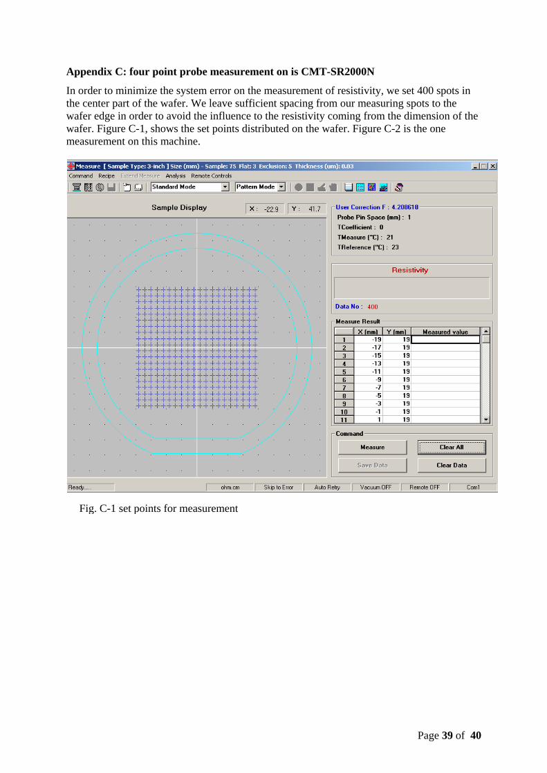
Appendix C: four point probe measurement on is CMT-SR2000N
In order to minimize the system error on the measurement of resistivity, we set 400 spots in the center part of the wafer. We leave sufficient spacing from our measuring spots to the wafer edge in order to avoid the influence to the resistivity coming from the dimension of the wafer. Figure C-1, shows the set points distributed on the wafer. Figure C-2 is the one measurement on this machine.
Fig. C-1 set points for measurement
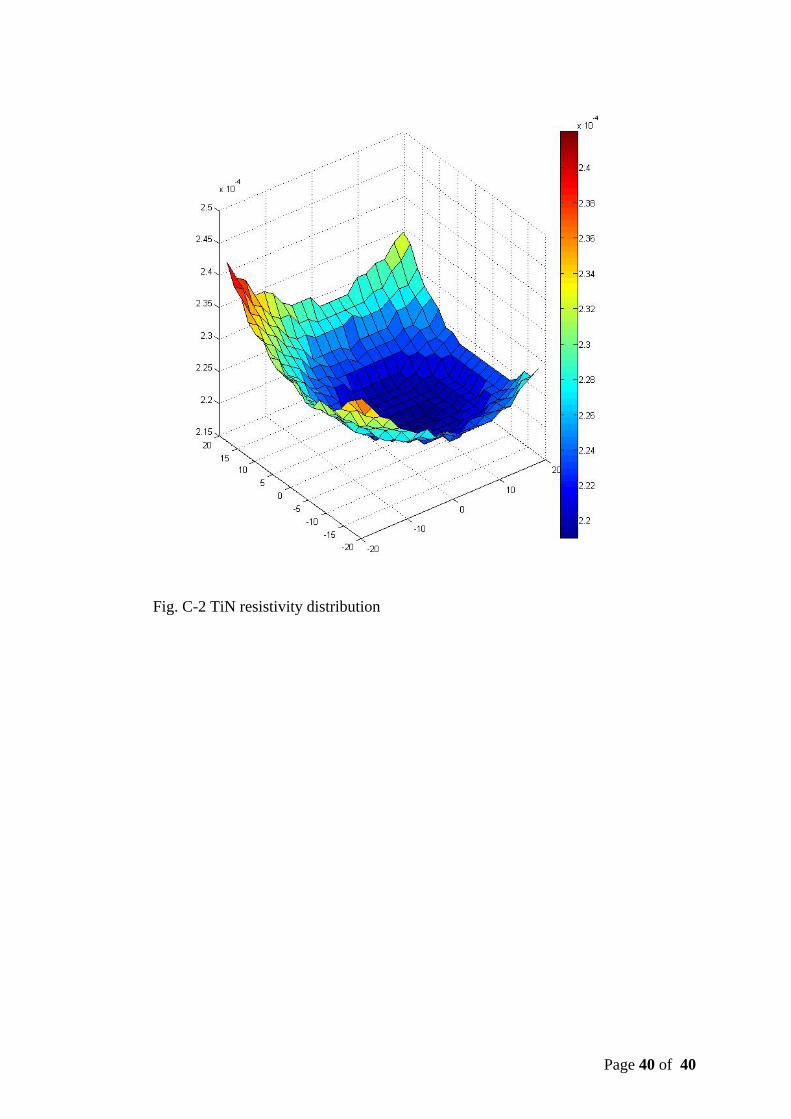
Page 40 of 40
Fig. C-2 TiN resistivity distribution