Embed Size (px)
Citation preview

MAHARASHTRA STATE BOARD OF TECHNICAL EDUCATION
(Autonomous)
(ISO/IEC - 27001 - 2005 Certified)
____________________________________________________________________________________
Page 1 of 28
SUMMER– 15 EXAMINATION
Subject Code: 17440 Model Answer
Important Instructions to examiners:
1) The answers should be examined by key words and not as word-to-word as given in the
model answer scheme.
2) The model answer and the answer written by candidate may vary but the examiner may try
to assess the understanding level of the candidate.
3) The language errors such as grammatical, spelling errors should not be given more
Importance (Not applicable for subject English and Communication Skills.
4) While assessing figures, examiner may give credit for principal components indicated in the
figure. The figures drawn by candidate and model answer may vary. The examiner may give
credit for any equivalent figure drawn.
5) Credits may be given step wise for numerical problems. In some cases, the assumed constant
values may vary and there may be some difference in the candidate’s answers and model answer.
6) In case of some questions credit may be given by judgement on part of examiner of relevant
answer based on candidate’s understanding.
7) For programming language papers, credit may be given to any other program based on
equivalent concept.

MAHARASHTRA STATE BOARD OF TECHNICAL EDUCATION
(Autonomous)
(ISO/IEC - 27001 - 2005 Certified)
____________________________________________________________________________________
Page 2 of 28
Q.1 (A) Attempt any SIX of the following 12 marks
a) Write down different frequencies for following (frequency range):
1. Voice Frequency
2. High Frequency
3. IR Frequency
4. Visible Spectrum (light)
Ans: (Four Correct frequencies – ½ mark each)
Sr. No Frequency Range
1 Voice Frequency 300 Hz to 3kHz
2 High Frequency 3 MHz to 30 MHz
3 IR Frequency 30 THz to 430 THz
4 Visible Spectrum (light) 375 THz to 750 THz
b) Define modulation index of FM
Ans: (Correct definition – 2 marks)
Modulation Index of FM: It is defined as the ratio of Frequency Deviation (δ) to the
modulating signal frequency (fm).
(OR)
Modulation Index of FM is defined as mf =
=
c) Define Pulse Modulation. State its types.
Ans: (Correct definition – 1 mark, Both Types any two sub classification – 1 mark)
Pulse Modulation: It is defined as the modulation technique in which the various parameters of
carrier signal which is the train of periodic rectangular pulses changes in accordance with the
instantaneous value of modulating signal.
Types of Pulse Modulation:
Analog Pulse modulation ( ½ M )
PAM
PWM
PPM
Digital Pulse Modulation ( ½ M )
PCM
DM
ADM

MAHARASHTRA STATE BOARD OF TECHNICAL EDUCATION
(Autonomous)
(ISO/IEC - 27001 - 2005 Certified)
____________________________________________________________________________________
Page 3 of 28
d) What are the different types of FM Detectors?
Ans: (Any four correct types – 2 marks)
The different types of FM Detectors are:
1. Simple Slope Detector
2. Balanced Slope Detector
3. Ratio Detector
4. Phase Discriminator
5. FM Detector using Phase Locked Loop (PLL)
e) What is the purpose of keeping RF section before mixer stage?
Ans: (Any two relevant correct points – 2 marks)
A radio receiver always has a RF section before the mixer stage because:
1. It selects the wanted frequency and rejects the unwanted frequencies.
2. Amplifier improves quality of receiver output and removes noise from received signal.
3. Better coupling of receiver to the antenna.
4. Prevention in the reradiation of the local oscillator through the antenna of the receiver.
f) Define Stub. State its two advantages.
Ans: (Definition – 1 mark, any two advantages – 1 mark)
Stub is the piece of short circuited transmission line which is used to tune out the reactance of the
load when connected across the transmission line as close as possible.
Advantages of Stub:
1. The load and source impedance is perfectly matched.
2. Maximum power transfer to the load.
3. It acts as a series resonant circuit to eliminate the interfering RF signals.
g) What are the different types of wave propagation?
Ans: (Any four correct types – 2 marks)
The different types of wave propagation are:
1. Ground Wave Propagation
2. Space Wave Propagation
3. Sky Wave Propagation / Ionospheric Propagation
4. Tropospheric Scatter Propagation
5. Duct Propagation
h) Define antenna resistance and antenna gain.
Ans: (each correct definition – 1 mark)
Antenna Resistance –
The resistance of an antenna has two components:
1. Its radiation resistance due to conversion of power into electromagnetic waves
2. The resistance due to actual losses in the antenna.
Antenna Gain –
The directional antennae radiate more power in certain direction. The Omni-directional antenna
radiates information equally in all directions.

MAHARASHTRA STATE BOARD OF TECHNICAL EDUCATION
(Autonomous)
(ISO/IEC - 27001 - 2005 Certified)
____________________________________________________________________________________
Page 4 of 28
A directional antenna is said to have ‘gain’ in a particular direction.
Q 1 (B) Attempt any TWO of the following 8 marks
a) Draw Yagi-Uda antenna with its radiation pattern.
Ans: (Construction – 2 marks, Radiation Pattern – 2 marks)
b) Compare ground wave and sky wave propagation for four points.
Ans: (Any Four relevant correct points – 1 mark each)
Sr. No Parameters Ground Wave Propagation Sky Wave Propagation
1 Frequency Range 30 kHz to 3 MHz 3 MHz to 30 MHz
2 Polarization Vertical Vertical
3 Applications Radio Broadcasting (MW
Range)
Radio Broadcasting (SW
Range)
4 Range of
Communication
Less (OR)
Few hundred Km
More (OR)
Few Thousand Km
5 Limitations Limited Range, Tall
Antenna Required, High
transmission power.
Skip Distance, Power loss
due to absorption of energy
in layers.
6 Fading Problem Less Severe

MAHARASHTRA STATE BOARD OF TECHNICAL EDUCATION
(Autonomous)
(ISO/IEC - 27001 - 2005 Certified)
____________________________________________________________________________________
Page 5 of 28
c) Draw the block diagram of basic electronic communication system. Describe its working
principle.
Ans: (block diagram – 2 marks, working principle – 2 marks)
The information source generates the information which may be analog or digital which is sent
to transmitter section where the information is amplified, filtered to remove noise, processed to
become compatible with the channel. For e.g. If channel is optical fiber then information is
converted into light energy.
The information from transmitter is sent to receiver through the communication
medium/channel. The channel may be wired (co-axial cable/optical fiber cable) or wireless
(microwave link).
The receiver again filters the information to remove noise, amplify, demodulates and convert the
information in the type which is compatible with the destination (for e.g. if destination is
computer the information is converted into digital binary form).
Q 2 Attempt any FOUR of the following 16 marks
a) Explain with circuit diagram PWM using IC 555.
Ans: (Circuit Diagram – 2 marks, operation – 2 marks)
Fig. Circuit of PWM generation using IC 555

MAHARASHTRA STATE BOARD OF TECHNICAL EDUCATION
(Autonomous)
(ISO/IEC - 27001 - 2005 Certified)
____________________________________________________________________________________
Page 6 of 28
Operation:
1. The timer IC555 is operated in Monostable mode.
2. The negative going carrier pulses are to the differentiator formed by R1 & C1. The
differentiator produces sharp negative pulses which are applied to trigger input pin (2) of IC
555.
3. These triggering decides the starting instants (leading edge) of the PWM pulses. The PWM
pulses go high at the instants of arrival of these triggering pulses.
4. The termination of the pulses is dependent upon,
R2, C2 discharge time
The modulating signal applied to control input pin (5)
5. The modulating signal applied to pin no (5) will vary the control voltage to IC 555 in
accordance to the modulating voltage.
6. As this voltage increases, the capacitor C2 is allowed to charge through R2 up to a higher
voltage & hence for a longer time (as R2 C2 time constant is fixed). The width of the
corresponding output pulse will increase due to this action. As soon as VC2 is equal to the
control voltage, the PWM pulse goes to zero.
7. Thus PWM signal is generated at the output pin (3) of IC555 as Monostable multivibrator.
b) Explain half wave dipole (resonant antenna) with its radiation pattern.
Ans: (Construction – 2 mark, explanation – 1 mark, radiation pattern – 1 mark)
Explanation: 1. It is a resonant antenna
2. It is exact half wavelength (λ /2) long & open circuited at one end.
3. The dipole antennas have lengths λ /2 , λ , 3 λ /2 etc. which are all multiple of λ /2. Hence
they are resonant.
4. In half wave dipole antennas the forward waves & reflected waves exist. Hence radiation
pattern is bidirectional.
5. The radiation pattern of half wave dipole antenna is -

MAHARASHTRA STATE BOARD OF TECHNICAL EDUCATION
(Autonomous)
(ISO/IEC - 27001 - 2005 Certified)
____________________________________________________________________________________
Page 7 of 28
c) Differentiate between simplex and duplex mode of communication.
Ans: (Two points – 2 marks, Diagram – 2 marks)
Sr.
No
Simplex Communication Duplex Communication
Half Duplex Full Duplex
1 It’s a one way communication
(unidirectional)
It’s a two way Communication
(bidirectional) but
simultaneous data transfer is
not possible.
It’s a two way
Communication
(bidirectional) with
simultaneous data transfer.
2 Eg: Television, Radio Eg: Walkie – Talkie Eg: Mobile
3
d) Draw block diagram of AM super heterodyne receiver and explain its working principle.
Ans: (diagram – 2 marks, principle – 2 marks)

MAHARASHTRA STATE BOARD OF TECHNICAL EDUCATION
(Autonomous)
(ISO/IEC - 27001 - 2005 Certified)
____________________________________________________________________________________
Page 8 of 28
AM super heterodyne receiver works on the principle of super heterodyning.
In the super heterodyne receiver, the incoming signal voltage is combined with a signal
generated in the receiver. The local oscillator voltage is normally converted into a signal of a low
fixed frequency with the help of mixer.
The signal at this intermediate frequency contains the same modulation as the original carrier and
it is now amplified and detected to reproduce the original modulating signal.
e) Write a mathematical expression for amplitude modulated wave.
Ans: (Correct equation – 4 marks)
eAM = Ec cos ωct +
cos(ωc + ωm)t +
cos(ωc - ωm)t
where, eAM – Instantaneous value of Amplitude Modulated Wave.
Ec – Peak voltage of Carrier signal.
m – Modulation Index of AM wave.
f) Draw and explain equivalent circuit of a transmission line.
Ans: (Circuit – 2 marks, explanation – 2 marks)
Transmission line is a medium of transmitting the signal over longer distances and so each
conductor has a certain length and diameter.
Since each conductor has a certain length and diameter it must have inductance and resistance.
R is the resistance in ohms per unit length while L is inductance per unit length in Henry.
Since wires are separated by a medium called dielectric which is not a perfect insulator, some
current will flow through it from one conductor to other. This will generate conductance G
measured in Siemens.
Also a small capacitance will be generated between the two conductors since in a cable
conductors will be separated by insulators which act as dielectric between the conductors.

MAHARASHTRA STATE BOARD OF TECHNICAL EDUCATION
(Autonomous)
(ISO/IEC - 27001 - 2005 Certified)
____________________________________________________________________________________
Page 9 of 28
Q. 3 Attempt any FOUR from the following. 16 marks
a) Explain the working of varactor diode reactance modulator for FM generation.
Ans: (Diagram- 2marks, Explanation-2marks)
Note: Any relevant correct diagram with explanation should be considered
Varactor diodes may be used to produce frequency modulation; they are employed with
reactance modulator, to provide automatic correction for FM transmitter.
Working:
The L1 and C1 represent the tuned circuit of the carrier oscillator.
The value of C2 is made very large at the operating frequency so that its reactance is very
low.
As a result, when C2 is connected in series with the lower capacitance of D1, the effect of D1
were connected directly across the tuned circuit.
The total effective circuit capacitance then is the capacitance of D1 in parallel with C1. This
fixes the carrier frequency.
The capacitance of D1 is controlled by two factors: a fixed d.c. bias and the modulating
signal.
The bias on D1 is set by the voltage divider which is made by R1 and R2.
The modulating signal is applied through C3 and RFC.
The C3 is a blocking capacitor that keeps the dc bias out of the modulating signal circuits.
As the modulating signal varies, it ads to and subtracts from the fixed bias voltage.
Thus, the effective voltage applied to D1 causes its capacitance to vary.
A positive going signal at point ‘A’ adds to the reverse bias, decreasing the capacitance and
increasing the carrier frequency.
A negative going signal at ‘A’ subtracts from the bias, increasing the capacitance and
decreasing the carrier frequency.
This is nothing but FM.

MAHARASHTRA STATE BOARD OF TECHNICAL EDUCATION
(Autonomous)
(ISO/IEC - 27001 - 2005 Certified)
____________________________________________________________________________________
Page 10 of 28
b) A practical antenna has directive gain of 5dB radiate 1200 watt power. How much power an
isotropic antenna should radiate in order to have the same power density at the same distance?
Ans : (formula- 2marks, answer- 2marks)
Given: directive gain G = 5dB, power radiated = 1200W
To find: power radiated by isotropic antenna
G =
GdB = 5dB
G = Antilog GdB
G = 3.162
G =
Piso =
=
Piso = 379.4W
c) Explain standing waves with load terminal open circuit & short circuit.
Ans: (each circuit - 2 marks)
Standing waves: The forward and reflected waves on the incorrectly terminated transmission line
produce an interference pattern known as Standing waves.
The concept of Standing wave can be best understood by considering the two cases of impedance
mismatch at load or the antenna end of the transmission line.
i) Short circuit:

MAHARASHTRA STATE BOARD OF TECHNICAL EDUCATION
(Autonomous)
(ISO/IEC - 27001 - 2005 Certified)
____________________________________________________________________________________
Page 11 of 28
The waveform below the transmission line shows the voltage and current at each point on
the line.
We can measure these voltages and current at each point with the help of multimeter.
As shown the voltage is zero while the current is maximum because short circuit means
zero impedance.
All the power is reflected back towards the source.
The voltage and current variations distribute themselves according to the wavelength of the
signal.
The pattern repeats for every one-half wavelength.
The voltage and current levels at the source will be dependent on the signal wavelength and
actual line.
ii) Open Circuit:
It means infinite impedance, so that voltage at the end of the line is maximum and the
current is zero.
All the energy is reflected, thereby setting up this stationary pattern of voltage and current
standing waves.
Practically, transmission line won’t have a short or open.
Instead, the load impedance will not be equal to the transmission line (characteristics)
impedance.

MAHARASHTRA STATE BOARD OF TECHNICAL EDUCATION
(Autonomous)
(ISO/IEC - 27001 - 2005 Certified)
____________________________________________________________________________________
Page 12 of 28
d) Explain Duct propagation.
Ans: (Diagram- 2marks, Explanation-2marks)
Duct propagation is a special type and used for very high microwave frequencies.
New phenomenon which occurs in super-refraction, also known as ducting.
As the height above earth increases, the air density decreases and refractive index increases.
Under certain special atmospheric conditions, a layer of warm air may be trapped above
cooler air, often over the surface of water.
So that refractive index will decrease far more rapidly with height than is usual.
This happens near ground within 30 m of it.
Due to this rapid reduction of refractive index, the microwaves completely bend back
towards earth surface as shown in fig.
Microwaves are thus continuously refracted in duct and reflected back by the ground, so that
they are propagated around the curvature of the earth for distances which many of times
exceed 1000km.
The main requirement of formation of atmospheric ducts is the so-called temperature
inversion.
Temperature inversion is the increase of air temperature with height, instead of the usual
decrease in temperature of 6.50C/km in the standard atmosphere.
The Duct propagation is used for very high frequencies in GHz range.

MAHARASHTRA STATE BOARD OF TECHNICAL EDUCATION
(Autonomous)
(ISO/IEC - 27001 - 2005 Certified)
____________________________________________________________________________________
Page 13 of 28
e) Define Image Frequency. The RF, local oscillator frequency, IF frequency for AM Receiver is
800KHz, 1255KHz & 455KHz respectively. Determine image frequency.
Ans: (Definition- 2marks, formula- 1mark, answer- 1mark)
Image frequency is defined as the signal frequency plus twice the intermediate frequency. It is
denoted as Fsi.
Fsi = Fs + 2Fi
Where Fs – Signal frequency
Fi – intermediate frequency
Given: Fs = 800KHz (RF signal frequency)
Fo = 1255KHz (local oscillator frequency)
Fsi = 455KHz (IF frequency)
Fsi = Fs + 2Fi &
Fi = Fo – Fsi
Fi = 1255 – 455
Fi = 800 KHz
Fsi = 800 x 103 + 2 x 800 x 10
3
= 2400 KHz
f) Explain power relation in AM wave.
Ans:
i) The Total power in AM (Pt) :
Pt = (Carrier power) + (Power in USB) + (Power in LSB)
Pt = PC + PUSB + PLSB
Pt =
+
+
(1 mark)
Where, Ercarr, ErUSB, ErLSB = R.M.S. values of the carrier and side band amplitudes
R = characteristics resistance of antenna in which total power is dissipated.

MAHARASHTRA STATE BOARD OF TECHNICAL EDUCATION
(Autonomous)
(ISO/IEC - 27001 - 2005 Certified)
____________________________________________________________________________________
Page 14 of 28
ii) Carrier power (Pc):
Pc =
= √
Pc =
(1 mark)
Where, Ec = Peak carrier amplitude
iii) Power in sidebands:
The power in USB and LSB is same as,
PUSB = PLSB =
Peak amplitude of sideband =
PUSB = PLSB = √
=
PUSB = PLSB =
X
= Pc
PUSB = PLSB =
Pc (1 mark)
iv) Total power in AM :
The total power in AM is,
Pt = Pc + PUSB + PLSB
= Pc +
Pc +
Pc
Pt = (1 +
) Pc (1 mark)

MAHARASHTRA STATE BOARD OF TECHNICAL EDUCATION
(Autonomous)
(ISO/IEC - 27001 - 2005 Certified)
____________________________________________________________________________________
Page 15 of 28
Q. 4 Attempt any FOUR from the following. 16 marks
a) Draw and explain circuit of AM modulator using BJT.
Ans: (Diagram- 2marks, Explanation-2marks)
Note: Any relevant correct circuit with explanation should be considered
AM modulator circuit is use to get the amplitude modulated signal as output.
The transistor is normally operated in the class c mode in which it is biased well beyond
cut-off.
The carrier input to the base must be sufficient to drive the transistor into conduction over
the part of RF cycle, during which collector current flows in the form of pulses.
The tuned circuit in the collector is tuned to resonate at the fundamental component, thus,
the RF voltage at the collector is sinusoidal.
When modulating signal is applied to the steady collector voltage, changes to a slowly
varying voltage given by V’cc = Vcc + Vm(t).
The modulating voltage Vm(t) is applied in series with Vcc through the low frequency
transformer.
The RF bypass capacitor provides a low impedance path for the RF to ground so that
negligible RF voltage is developed across the LF transformer secondary.
The modulated output is obtained through mutual inductive coupling.
The coupling prevents the steady voltage from being transferred to the output, so that Rf
varies about mean value of zero.

MAHARASHTRA STATE BOARD OF TECHNICAL EDUCATION
(Autonomous)
(ISO/IEC - 27001 - 2005 Certified)
____________________________________________________________________________________
Page 16 of 28
b) Compare the bandwidth that would be required to transmit baseband signal with a frequency
range from 300Hz to 3 KHz using
i) Narrow band FM with maximum deviation of 5 KHz
ii) Wideband FM with maximum deviation of 75 KHz.
Ans: (Formula each – 1mark, Answer each – 1 mark)
i) For Narrow band FM
Max modulating frequency is for baseband signal range (Fm) = 300Hz to 3KHz
Frequency deviation (δ) given is 5KHz
BW = 2(δ + Fm)
= 2 (5 + 3)
= 16 KHz
ii) For Wideband FM
Max Wideband frequency (Fm) = 5KHz
Frequency deviation (δ) given is = 75KHz
BW = 2(δ + Fm)
= 2 (75 + 10)
= 2 X 90
= 180 KHz
c) Explain working of Balun with diagram.
Ans: (Diagram- 2marks, Explanation-2marks)

MAHARASHTRA STATE BOARD OF TECHNICAL EDUCATION
(Autonomous)
(ISO/IEC - 27001 - 2005 Certified)
____________________________________________________________________________________
Page 17 of 28
1. A Balun or a balance to unbalance transformer, is a circuit element used to connect a
balanced line to unbalanced line. i.e. it is used to connect an unbalanced (coaxial) line to a
balance antenna such as a dipole.
2. As shown in fig. here the windings associated with the balanced system is symmetrically
arranged with respect to a grounded electrostatic shield so that stray capacitances inevitably
present will not introduce unbalance.
3. At high frequencies, several transmission line baluns used for differing purposes and narrow
band or broadband application.
e.g. if impedance of parallel wire is 300 and co-axial is 75 then,
Zo = √ = √ = 150
4. The most common balun a narrow band one shown in fig. it is known as choke, sleeve or
bazooka balun.
d) Explain i) critical frequency ii) skip distance
Ans: (Each explanation - 2 marks)
i) Critical frequency: The critical frequency of a layer is defined as the maximum frequency
that is returned back to the earth by that layer, when the wave is incident at an angle 900
(normal)
to it.
The critical frequency for F2 layer is between 5 to 12 MHz
ii) Skip distance: The skip distance is defined as the shortest distance from a transmitter,
measured along the surface of earth at which a sky wave of fixed frequency returns back to the
earth.
The frequency should be greater than critical frequency fc .

MAHARASHTRA STATE BOARD OF TECHNICAL EDUCATION
(Autonomous)
(ISO/IEC - 27001 - 2005 Certified)
____________________________________________________________________________________
Page 18 of 28
e) What are different microwave antennas? Explain horn antenna.
Ans: (List 2 Antennas– 1 mark, any one diagram of horn antenna – 1mark, explanation- 2
marks)
Types of microwave antennas: i) Dish antenna ii) Horn antenna
Horn antenna:
1. It is basically a waveguide terminated by horn.
2. Waveguide is a hollow metallic pipe used to carry electromagnetic waves at microwave
frequencies.
3. All the energy travelling forward in the waveguide is radiated very effectively with the
addition of the horn.
4. There are three configuration s of most commonly used Horn antennas, i) Sectorial ii)
Pyramidal iii) Conical
As shown in fig.
i) The Sectorial horn flares out only in one direction.
ii) Pyramidal horn flares out in both directions and has the shape of truncated pyramid.
iii) The Conical horn is the termination of a circular waveguide.
The ratio of L/ decides the beam width and the gain of the antenna.
There are two types of Horn antenna
a) Cass- horn antenna
b) Hog Horn antenna

MAHARASHTRA STATE BOARD OF TECHNICAL EDUCATION
(Autonomous)
(ISO/IEC - 27001 - 2005 Certified)
____________________________________________________________________________________
Page 19 of 28
f) Explain single & double stub matching. Ans. (Each type - 2 marks) Single stub: Stub is the piece of short circuited TL which is used to tune out the reactance of the load when connected across the TL as close as possible. 1. The most important feature of single stub matching is that the stub should be located as near
to the load as possible.
2. The characteristic admittance of the stub so connected in shunt should be same as that of the main line.
3. The main element of this transmission line is a short circuited section of line whose
open end is connected to the main line at a particular distance from the load end.
4. Where the input conductance at that point is equal to the characteristic conductance of the line, and the stub length is adjusted to provide a susceptance equal in value but opposite in sign, to the input susceptance of the main line at that point.
5. So the total susceptance of the main line at that point is zero. 6. The combination of stub and the line will thus present a conductance which is equal
to the characteristic impedance of the line, i.e. the main length of the HF
transmission line will be matched.

MAHARASHTRA STATE BOARD OF TECHNICAL EDUCATION
(Autonomous)
(ISO/IEC - 27001 - 2005 Certified)
____________________________________________________________________________________
Page 20 of 28
Double stub:
The disadvantages of single stub matching are overcome by using double stub matching as
shown in fig.
Here, two short circuited stubs at two fixed point usually /4 apart are utilized.
Their positions are fixed but lengths are independently adjustable.
The double stub matching provides wide range of impedance matching.
5. Attempt any FOUR from the following 16 marks
a) Explain the working of De-emphasis circuit.
Ans:- (Diagram – 2marks, explanation- 2 marks)

MAHARASHTRA STATE BOARD OF TECHNICAL EDUCATION
(Autonomous)
(ISO/IEC - 27001 - 2005 Certified)
____________________________________________________________________________________
Page 21 of 28
In FM, noise has greater effect on higher modulating frequencies than the lower one. Therefore
the higher modulating frequencies have to be boosted artificially at the transmitter before
modulation and corresponding cut off at the receiver after demodulation.
This boosting of higher modulation frequencies at the transmitter in order to improve noise
immunity is called as pre-emphasis. The compensation at the receiver ie. Attenuation of this
higher modulation frequency after detector at receiver is called as De-emphasis, which is
basically a low pass filter.
Pre-emphasis is used at transmitter and de-emphasis at receiver to o\improve the noise immunity.
b) Draw block diagram of FM receiver.
Ans:-(Correct diagram – 4 marks)
c) Explain quarter wavelength transformer.
Ans :-( Diagram – 1 marks, explanation- 3 marks)
In all applications of transmission line, it is required that the load be matched to line, which
requires tuning out the unwanted load reactance and the transformation of resulting impedance
to the required value especially at high frequencies.
The impedance of the quarter line depends on load impedance and characteristics impedance as
shown-
MAHARASHTRA STATE BOARD OF TECHNICAL EDUCATION
(Autonomous)
(ISO/IEC - 27001 - 2005 Certified)
____________________________________________________________________________________
Page 22 of 28
When the length S is exactly quarter wavelength line then the line is lossless. If the Zo is varied,
the impedance seen at the input to the λ/4 transformer will also vary accordingly, so that load
may be matched to characteristic impedance of the main line. This is similar to varying truns
ration of a transformer to obtain the required value of inpur impedance to match the load
impedance. Quarter wave transformer works as filter to prevent unwanted frequencies from
reaching the load such as antenna.
The name transformer is given to quarter wavelength transmission line since it behaves as a
transformer depending upon the value of ZL.
If ZL = Zo then it acts as 1 : 1 transformer.
If ZL > Zo then it acts as a Step down transformer
If ZL < Zo then it acts as a Step up transformer
d) The operating frequency for pyramidal horn antenna is 10 GHz. The horn antenna is 10 cm
high and 12 cm wide. Calculate
1) Beam width of antenna
2) Power gain of antenna if K=5.
Ans: - (Beam width – 2 marks, Power gain – 2 marks)
Given: w = 12 cm = 0.12m, H = 10 cm = 0.10m
Operating frequency = 10GHz
To find: Beam width of antenna =?
Power Gain if K = 5?
Solution:
We have,
Beam width = BW =
for width w
Beam width = BH =
for width H
Power gain G =
where K = 5
λ =
=
= 0.03
A =Aperture in meters = w x H
= 0.12 x 0.10 = 0.012m2
BW =
= 20
Therefore, BW in dB = 10 log 20
= 13 dB
Therefore BW = 13 dB (1 mark)

MAHARASHTRA STATE BOARD OF TECHNICAL EDUCATION
(Autonomous)
(ISO/IEC - 27001 - 2005 Certified)
____________________________________________________________________________________
Page 23 of 28
BH =
= 24
Therefore, BW in dB = 10 log 24
= 13.8 dB
Therefore BW = 13.8 dB (1 mark)
Power gain G =
=
= 837.75
Gain in dB = 10 log 837.7 = 29.23 dB
Therefore, Gain in dB = 29.23 dB (2 marks)
e) Explain the working of FM demodulator using phase lock loop with the help of circuit
diagram.
Ans:- (Diagram – 2marks, explanation- 2 marks)
Explanation:-
FM signal which is to be demodulated is applied to input of PLL.VCO output must be
identical to input signal if PLL is to remain locked.
As PLL is locked, VCO starts tracking the instantaneous frequency in the FM input signal
The error voltage produced at the output of the amplifier is proportional to the deviation of
the input frequency from the center frequency FM.
Thus AC component of the error voltage represents the modulating signal. Thus at the error
amplifier output we get demodulated FM output.
f) State the different losses in transmission line.
Ans: -(Any four losses – 4 marks)
Losses in transmission line:-
1) Conductor loss
2) Dielectric heating loss
3) Radiation loss
4) Coupling loss
5) Corona
MAHARASHTRA STATE BOARD OF TECHNICAL EDUCATION
(Autonomous)
(ISO/IEC - 27001 - 2005 Certified)
____________________________________________________________________________________
Page 24 of 28
6. Attempt any FOUR from the following 16 marks
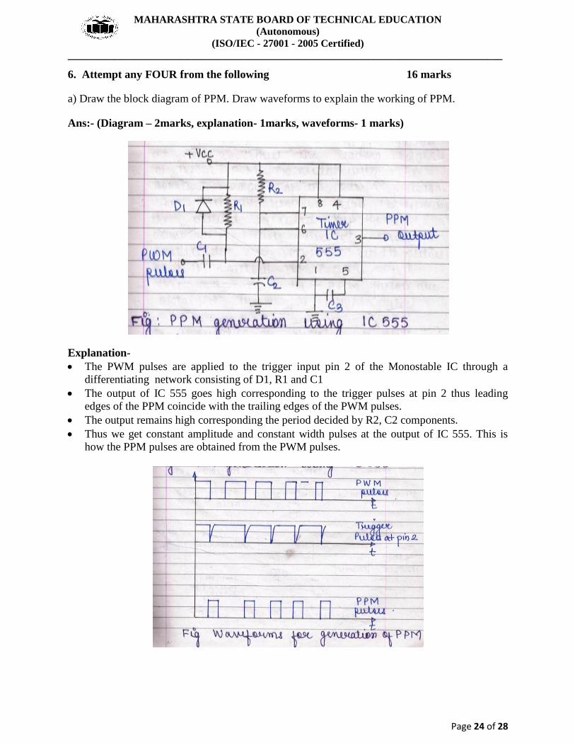
a) Draw the block diagram of PPM. Draw waveforms to explain the working of PPM.
Ans:- (Diagram – 2marks, explanation- 1marks, waveforms- 1 marks)
Explanation-
The PWM pulses are applied to the trigger input pin 2 of the Monostable IC through a
differentiating network consisting of D1, R1 and C1
The output of IC 555 goes high corresponding to the trigger pulses at pin 2 thus leading
edges of the PPM coincide with the trailing edges of the PWM pulses.
The output remains high corresponding the period decided by R2, C2 components.
Thus we get constant amplitude and constant width pulses at the output of IC 555. This is
how the PPM pulses are obtained from the PWM pulses.

MAHARASHTRA STATE BOARD OF TECHNICAL EDUCATION
(Autonomous)
(ISO/IEC - 27001 - 2005 Certified)
____________________________________________________________________________________
Page 25 of 28
b) Explain the sensitivity and selectivity for AM radio receiver.
Ans:-
Sensitivity:
The ability to amplify weak signals is called sensitivity. The sensitivity is expressed in millivolt.
It is often defined in terms of the input voltage that must be applied at the input of the receiver to
obtain a standard output power.
The sensitivity curve indicates that the receiver input required to obtain the same standard output
changes with carrier frequency. (1 mark)
Graph: (1 mark)
Selectivity:
The ability of radio receiver to reject the unwanted signals is called selectivity. It shows that the
receiver offers a minimum rejection at 950 kHz but the rejection increases as the input signal
frequency deviates on both sides of 950 kHz. The selectivity decides the adjacent channel
rejection of a receiver. (1 mark)
Graph- (1 mark)

MAHARASHTRA STATE BOARD OF TECHNICAL EDUCATION
(Autonomous)
(ISO/IEC - 27001 - 2005 Certified)
____________________________________________________________________________________
Page 26 of 28
c) Explain the working of phase discriminator FM.
Ans:- (Diagram – 2marks, explanation- 2 marks)
Explanation-
This discriminator is also known as the center tuned discriminator or the Foster Seeley
discriminator after its inventors. It is possible to obtain the same S- Shape response curve
from a circuit in which the primary & the secondary winding are both tuned to the center
frequency of the incoming signal. This is desirable because it greatly simplifies alignment &
also because the process yields far better linearity.
Thus although the individual component voltage will be the same at the diode input at all
frequencies, the vector sums will differ with the phase difference between primary &
secondary windings. The result will be that the individual output voltage will be equal only at
f.
At all other frequencies the output of one diode will be greater than that of the other. Which
diode has the larger output will depend entirely on whether fm is above or below fc. As for
the output arrangements, it will be positive or negative according to the input frequency. As
required the magnitude of the output will depend on the deviation of the input frequency
from fc.
d) Explain demodulation of AM signal using practical diode detector.
Ans:- (Diagram – 2marks, explanation- 1 marks, waveforms -1 marks)
MAHARASHTRA STATE BOARD OF TECHNICAL EDUCATION
(Autonomous)
(ISO/IEC - 27001 - 2005 Certified)
____________________________________________________________________________________
Page 27 of 28
Explanation- The circuit operates in the following manner-
The diode has been reversed so that now the negative envelope is demodulated. Due to this
negative envelope AGC voltage will be developed.R1 and R2 ensures that there is a series
DC path to ground for diode.
R1 and C1 is the low pass used to remove RF ripple that is present in the detector o/p.C2 is
coupling capacitor that prevents the diode DC o/p from reaching the volume control R4.
R3 and C3 is a low pass filter which removes AF components and helps to produce AGC
voltage.
The DC AGC voltage is proportional to the amplitude of AM signal.
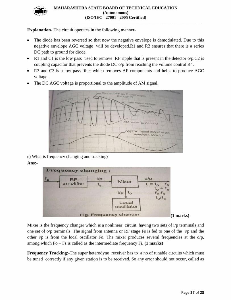
e) What is frequency changing and tracking?
Ans:-
(1 marks)
Mixer is the frequency changer which is a nonlinear circuit, having two sets of i/p terminals and
one set of o/p terminals. The signal from antenna or RF stage Fs is fed to one of the i/p and the
other i/p is from the local oscillator Fo. The mixer produces several frequencies at the o/p,
among which Fo – Fs is called as the intermediate frequency Fi. (1 marks)
Frequency Tracking:-The super heterodyne receiver has to a no of tunable circuits which must
be tuned correctly if any given station is to be received. So any error should not occur, called as

MAHARASHTRA STATE BOARD OF TECHNICAL EDUCATION
(Autonomous)
(ISO/IEC - 27001 - 2005 Certified)
____________________________________________________________________________________
Page 28 of 28
tracking errors Thus frequency tracking is the process in which the local oscillator frequency
follows or tracks the signal frequency to have a correct frequency difference for IF stage.
There are two types of tracking-
a) two point tracking
b) three point tracking (2 marks)
f) For 2 meter diameter parabolic reflector with 10 watt of power radiated by the feed mechanism
operating at 6 GHz with transmit antenna efficiency of 55%. Determine
1) beam width of antenna
2) transmit power gain
Ans: (Beam width – 2 marks, Transmit power gain – 2 marks)
Given: f = 6 GHz
% Efficiency ɳ = 0.55
λ =
=
= 0.05
K = 70, D = 2m
To find: Beam width =?
Power Gain =?
Solution:
Transmit Power gain
G = ɳ x (
)
= 0.55 x (
)
G = 15791.36
G in dB = 10 log G
= 41.98 dB
Therefore, G = 41.98 dB
Beam width = Half power beam width
= α =
=
= 1.75
0