Embed Size (px)
Citation preview

MAHARASHTRA STATE BOARD OF TECHNICAL EDUCATION (Autonomous)
(ISO/IEC - 27001 - 2013 Certified)
SUMMER– 18 EXAMINATION Subject Name: Power Electronics Model Answer Subject Code:
__________________________________________________________________________________________________
Page NO:1/37
17444
Important Instructions to examiners:
1) The answers should be examined by key words and not as word-to-word as given in the model answer scheme.
2) The model answer and the answer written by candidate may vary but the examiner may try to assess the understanding level of the candidate.
3) The language errors such as grammatical, spelling errors should not be given more Importance (Not applicable for subject English and Communication Skills.
4) While assessing figures, examiner may give credit for principal components indicated in the figure. The figures drawn by candidate and model answer may vary. The examiner may give credit for any equivalent figure drawn.
5) Credits may be given step wise for numerical problems. In some cases, the assumed constant values may vary and there may be some difference in the candidate’s answers and model answer.
6) In case of some questions credit may be given by judgement on part of examiner of relevant answer based on candidate’s understanding.
7) For programming language papers, credit may be given to any other program based on equivalent concept.
Q. No.
Sub Q. N.
Answers Marking Scheme
1 A Attempt any SIX: 12- Total Marks
a Name any two triggering devices used for triggering SCR. 2M
Ans: UJT, PUT, SUS,LASCR 1M each for any two
b State any two advantages of IGBT. 2M
Ans: 1) High operating speed 2) Wide RBSOA 3) High voltage control capability 4) Active di/dt control 5) Inherent over-current protection
1M each for any two
c List two applications of TRIAC. 2M
Ans: TRIAC is used as a switching device in the following applications:
1) Fan speed regulator 2) Flasher circuit 3) Temperature controller 4) Lamp dimmer
1M each for any two

MAHARASHTRA STATE BOARD OF TECHNICAL EDUCATION (Autonomous)
(ISO/IEC - 27001 - 2013 Certified)
SUMMER– 18 EXAMINATION Subject Name: Power Electronics Model Answer Subject Code:
__________________________________________________________________________________________________
Page NO:2/37
17444
5) In AC voltage stabilizer 6) Proximity detector
d State the classification of Chopper. 2M
Ans: DC chopper can be classified as :
1.According to input/output voltage levels
a. Step –Up chopper
b. Step – Down chopper
2. According to direction of output voltage and current
a. Class A Chopper
b. Class B Chopper
c. Class C Chopper
d. Class D Chopper
e. Class E Chopper
3. According to Circuit operation
a. First Quadrant Chopper
b. Two quadrant Chopper
c. Four Quadrant Chopper
4. According to Commutation method
a. Voltage Commuted Chopper
b. Current Commuted Chopper
c. Load Commuted Chopper
d. Impulse Commuted Chopper
2M
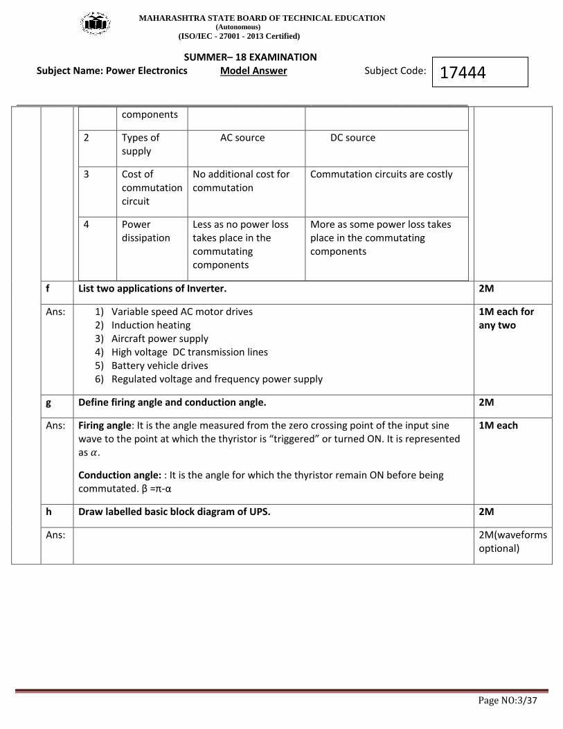
e State difference between forced commutation and natural commutation.(any 2 points)
2M
Ans: Sr No. Parameter Natural commutation Forced commutation
1 Need of external commutating
Not required Required
1M each for any two points
MAHARASHTRA STATE BOARD OF TECHNICAL EDUCATION (Autonomous)
(ISO/IEC - 27001 - 2013 Certified)
SUMMER– 18 EXAMINATION Subject Name: Power Electronics Model Answer Subject Code:
__________________________________________________________________________________________________
Page NO:3/37
17444
components
2 Types of supply
AC source DC source
3 Cost of commutation circuit
No additional cost for commutation
Commutation circuits are costly
4 Power dissipation
Less as no power loss takes place in the commutating components
More as some power loss takes place in the commutating components
f List two applications of Inverter. 2M
Ans: 1) Variable speed AC motor drives 2) Induction heating 3) Aircraft power supply 4) High voltage DC transmission lines 5) Battery vehicle drives 6) Regulated voltage and frequency power supply
1M each for any two
g Define firing angle and conduction angle. 2M
Ans: Firing angle: It is the angle measured from the zero crossing point of the input sine wave to the point at which the thyristor is “triggered” or turned ON. It is represented as .
Conduction angle: : It is the angle for which the thyristor remain ON before being commutated. β =π-α
1M each
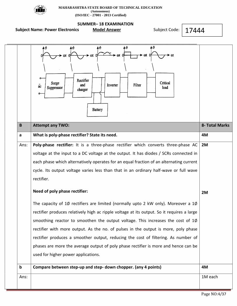
h Draw labelled basic block diagram of UPS. 2M
Ans: 2M(waveforms optional)
MAHARASHTRA STATE BOARD OF TECHNICAL EDUCATION (Autonomous)
(ISO/IEC - 27001 - 2013 Certified)
SUMMER– 18 EXAMINATION Subject Name: Power Electronics Model Answer Subject Code:
__________________________________________________________________________________________________
Page NO:4/37
17444
B Attempt any TWO: 8- Total Marks
a What is poly-phase rectifier? State its need. 4M
Ans: Poly-phase rectifier: It is a three-phase rectifier which converts three-phase AC
voltage at the input to a DC voltage at the output. It has diodes / SCRs connected in
each phase which alternatively operates for an equal fraction of an alternating current
cycle. Its output voltage varies less than that in an ordinary half-wave or full wave
rectifier.
Need of poly phase rectifier:
The capacity of 1 rectifiers are limited (normally upto 2 kW only). Moreover a 1
rectifier produces relatively high ac ripple voltage at its output. So it requires a large
smoothing reactor to smoothen the output voltage. This increases the cost of 1
rectifier with more output. As the no. of pulses in the output is more, poly phase
rectifier produces a smoother output, reducing the cost of filtering. As number of
phases are more the average output of poly phase rectifier is more and hence can be
used for higher power applications.
2M
2M
b Compare between step-up and step- down chopper. (any 4 points) 4M
Ans:
1M each
MAHARASHTRA STATE BOARD OF TECHNICAL EDUCATION (Autonomous)
(ISO/IEC - 27001 - 2013 Certified)
SUMMER– 18 EXAMINATION Subject Name: Power Electronics Model Answer Subject Code:
__________________________________________________________________________________________________
Page NO:5/37
17444
Sr No.
Parameter Step-up chopper Step-down chopper
1 Position of chopper switch
In parallel with load In series with load
2 Output voltage More than input voltage Less than input voltage
3 Expression of output voltage
Vo = Vdc / (1- ) Volts
Where,
= Duty Cycle
Vdc= Input voltage
Vo = Vdc. Volts
4 application Battery charging, voltage booster
Motor speed control
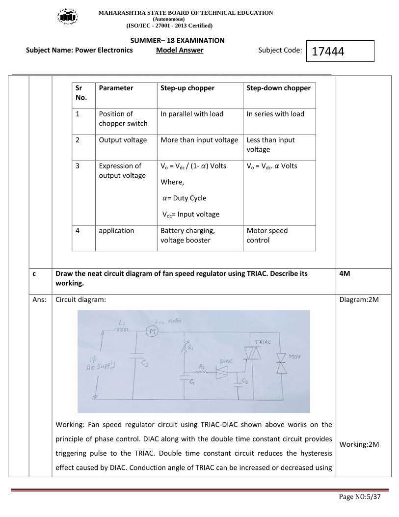
c Draw the neat circuit diagram of fan speed regulator using TRIAC. Describe its working.
4M
Ans: Circuit diagram:
Working: Fan speed regulator circuit using TRIAC-DIAC shown above works on the
principle of phase control. DIAC along with the double time constant circuit provides
triggering pulse to the TRIAC. Double time constant circuit reduces the hysteresis
effect caused by DIAC. Conduction angle of TRIAC can be increased or decreased using
Diagram:2M
Working:2M
MAHARASHTRA STATE BOARD OF TECHNICAL EDUCATION (Autonomous)
(ISO/IEC - 27001 - 2013 Certified)
SUMMER– 18 EXAMINATION Subject Name: Power Electronics Model Answer Subject Code:
__________________________________________________________________________________________________
Page NO:6/37
17444
R1. As R1 is reduced, the conduction angle of TRIAC increases increasing the output
voltage and speed of fan. A ‘MOV’ is connected parallel to the TRIAC to protect it
against voltage transients and surges.
Note: (any other relevant diagram may also be considered)
Q. No.
Sub Q. N.
Answers Marking Scheme
2 Attempt any FOUR: 16- Total Marks
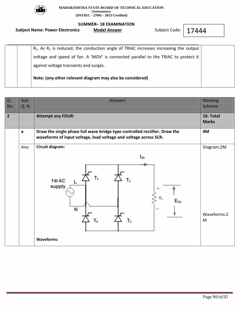
a Draw the single phase full wave bridge type controlled rectifier. Draw the waveforms of input voltage, load voltage and voltage across SCR.
4M
Ans: Circuit diagram:
Waveforms:
Diagram:2M
Waveforms:2M
MAHARASHTRA STATE BOARD OF TECHNICAL EDUCATION (Autonomous)
(ISO/IEC - 27001 - 2013 Certified)
SUMMER– 18 EXAMINATION Subject Name: Power Electronics Model Answer Subject Code:
__________________________________________________________________________________________________
Page NO:7/37
17444
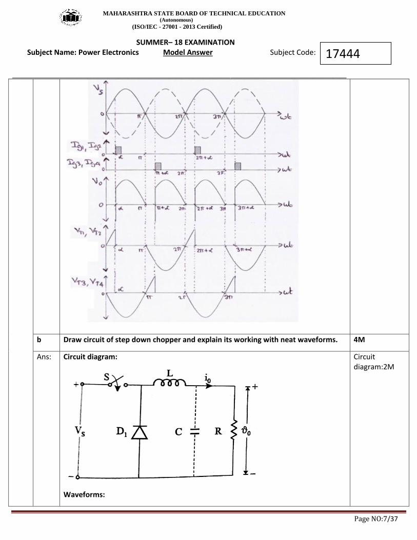
b Draw circuit of step down chopper and explain its working with neat waveforms. 4M
Ans: Circuit diagram:
Waveforms:
Circuit diagram:2M
MAHARASHTRA STATE BOARD OF TECHNICAL EDUCATION (Autonomous)
(ISO/IEC - 27001 - 2013 Certified)
SUMMER– 18 EXAMINATION Subject Name: Power Electronics Model Answer Subject Code:
__________________________________________________________________________________________________
Page NO:8/37
17444
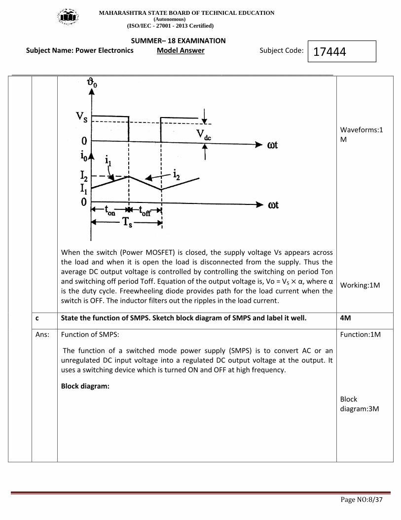
When the switch (Power MOSFET) is closed, the supply voltage Vs appears across the load and when it is open the load is disconnected from the supply. Thus the average DC output voltage is controlled by controlling the switching on period Ton and switching off period Toff. Equation of the output voltage is, Vo = VS α, where α is the duty cycle. Freewheeling diode provides path for the load current when the switch is OFF. The inductor filters out the ripples in the load current.
Waveforms:1M
Working:1M
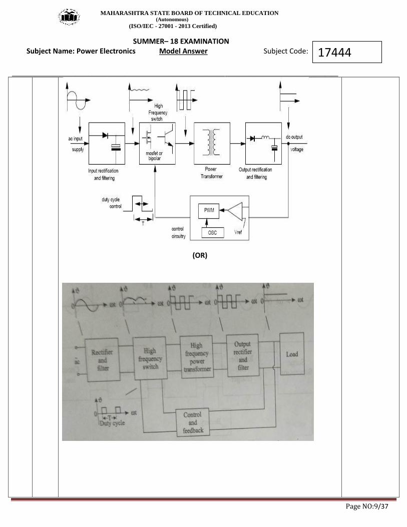
c State the function of SMPS. Sketch block diagram of SMPS and label it well. 4M
Ans: Function of SMPS:
The function of a switched mode power supply (SMPS) is to convert AC or an unregulated DC input voltage into a regulated DC output voltage at the output. It uses a switching device which is turned ON and OFF at high frequency.
Block diagram:
Function:1M
Block diagram:3M
MAHARASHTRA STATE BOARD OF TECHNICAL EDUCATION (Autonomous)
(ISO/IEC - 27001 - 2013 Certified)
SUMMER– 18 EXAMINATION Subject Name: Power Electronics Model Answer Subject Code:
__________________________________________________________________________________________________
Page NO:9/37
17444
(OR)
MAHARASHTRA STATE BOARD OF TECHNICAL EDUCATION (Autonomous)
(ISO/IEC - 27001 - 2013 Certified)
SUMMER– 18 EXAMINATION Subject Name: Power Electronics Model Answer Subject Code:
__________________________________________________________________________________________________
Page NO:10/37
17444
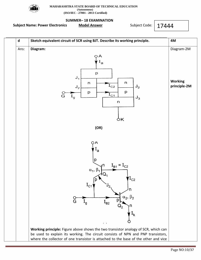
d Sketch equivalent circuit of SCR using BJT. Describe its working principle. 4M
Ans: Diagram:
(OR)
Working principle: Figure above shows the two transistor analogy of SCR, which can be used to explain its working. The circuit consists of NPN and PNP transistors, where the collector of one transistor is attached to the base of the other and vice
Diagram-2M
Working principle-2M
MAHARASHTRA STATE BOARD OF TECHNICAL EDUCATION (Autonomous)
(ISO/IEC - 27001 - 2013 Certified)
SUMMER– 18 EXAMINATION Subject Name: Power Electronics Model Answer Subject Code:
__________________________________________________________________________________________________
Page NO:11/37
17444
versa. When the gate is made positive a small input current flows between the base and emitter of Q2, producing a large collector current IC2. IC2 is the base current of Q1 cause a large base current for Q2. Therefore a positive feedback exist between the transistors making them to go into saturation. Equation for the anode current can be derived as
Where are the current gains of Q1 & Q2 respectively.
if =1, the value of infinite, or suddenly reaches a very high value and the SCR latches into conduction from an OFF state. This characteristics is known as regenerative action. According to this, the turn ON condition of a SCR is,
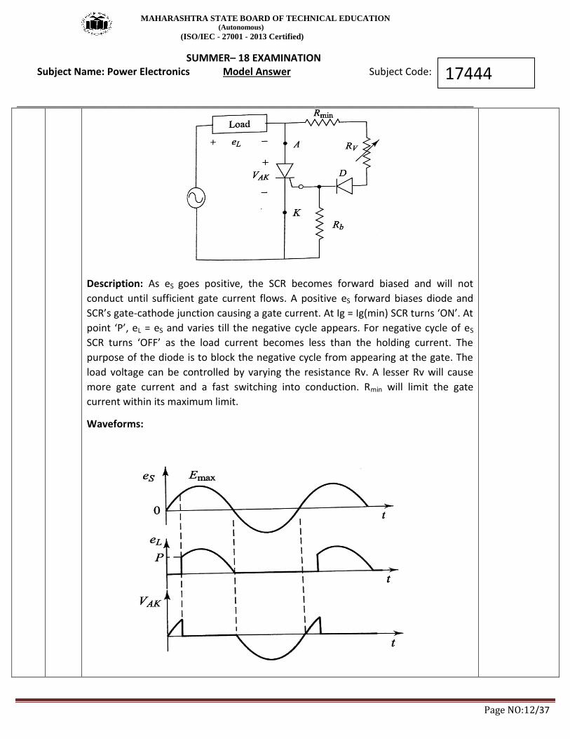
e State different trigger methods and describe R-triggering method for SCR with circuit diagram and waveforms.
4M
Ans: Different triggering methods of SCR are:
1. Forward voltage triggering
2. Thermal or temperature triggering
3. Radiation or Light triggering
4. dv/dt triggering
5. Gate triggering
i) D.C Gate triggering
ii) Pulse Gate triggering
iii) A.C Gate triggering
a) R-triggering b) RC-triggering
R-triggering:
Circuit diagram:
Listing-1M
Diagram-1M
Description-1M
Waveforms-1M
MAHARASHTRA STATE BOARD OF TECHNICAL EDUCATION (Autonomous)
(ISO/IEC - 27001 - 2013 Certified)
SUMMER– 18 EXAMINATION Subject Name: Power Electronics Model Answer Subject Code:
__________________________________________________________________________________________________
Page NO:12/37
17444
Description: As eS goes positive, the SCR becomes forward biased and will not
conduct until sufficient gate current flows. A positive eS forward biases diode and
SCR’s gate-cathode junction causing a gate current. At Ig = Ig(min) SCR turns ‘ON’. At
point ‘P’, eL = eS and varies till the negative cycle appears. For negative cycle of eS
SCR turns ‘OFF’ as the load current becomes less than the holding current. The
purpose of the diode is to block the negative cycle from appearing at the gate. The
load voltage can be controlled by varying the resistance Rv. A lesser Rv will cause
more gate current and a fast switching into conduction. Rmin will limit the gate
current within its maximum limit.
Waveforms:
MAHARASHTRA STATE BOARD OF TECHNICAL EDUCATION (Autonomous)
(ISO/IEC - 27001 - 2013 Certified)
SUMMER– 18 EXAMINATION Subject Name: Power Electronics Model Answer Subject Code:
__________________________________________________________________________________________________
Page NO:13/37
17444
f Define distortion factor and lowest order harmonics with respect to inverter. 4M
Ans: Distortion Factor (DF):
Distortion factor indicates the amount of harmonics that remain in the output voltage waveform, after the voltage waveform has been subjected to second order attenuation.
Lowest Order Harmonics(LOH):
The lowest frequency harmonic, with a magnitude greater than or equal to 3% of the magnitude of the fundamental component of the output voltage is known as lowest order harmonic.
2M each
Q. No.
Sub Q. N.
Answers Marking Scheme
3 Attempt any FOUR: 16- Total Marks
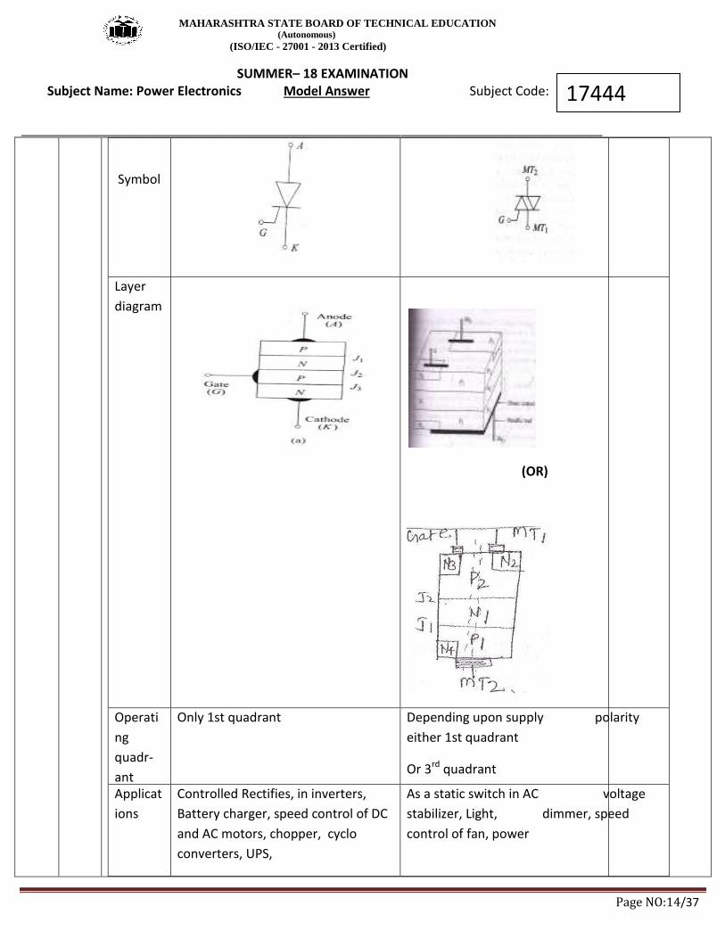
a Differentiate SCR and TRIAC with respect to (i) symbol, (ii) layered diagram, (iii) operating quadrant, (iv) application.
4M
Ans:
Parame
ter
SCR TRIAC
1M each
MAHARASHTRA STATE BOARD OF TECHNICAL EDUCATION (Autonomous)
(ISO/IEC - 27001 - 2013 Certified)
SUMMER– 18 EXAMINATION Subject Name: Power Electronics Model Answer Subject Code:
__________________________________________________________________________________________________
Page NO:14/37
17444
Symbol
Layer
diagram
(OR)
Operati
ng
quadr-
ant
qqqudra
ntquadr
ant
Only 1st quadrant
Depending upon supply polarity
either 1st quadrant
Or 3rd quadrant
or 3rd quadrant.
Applicat
ions
Controlled Rectifies, in inverters,
Battery charger, speed control of DC
and AC motors, chopper, cyclo
converters, UPS,
As a static switch in AC voltage
stabilizer, Light, dimmer, speed
control of fan, power
MAHARASHTRA STATE BOARD OF TECHNICAL EDUCATION (Autonomous)
(ISO/IEC - 27001 - 2013 Certified)
SUMMER– 18 EXAMINATION Subject Name: Power Electronics Model Answer Subject Code:
__________________________________________________________________________________________________
Page NO:15/37
17444
emergency lighting system, static
circuit breaker, flasher.
switches.
b Compare controlled and uncontrolled rectifiers. (any 4 points) 4M
Ans:
Parameter Controlled Rectifier Uncontrolled Rectifier
Device used SCR and Diodes Only Diodes.
Control of Load
Voltage
Load voltage can be
controlled.
Load voltage cannot
be controlled.
Direction of Power
Flow
Source to load and
sometimes load to source.
Source to load only.
Free Wheeling diode Required if inductive load. Not necessary.
Triggering circuit Required. Not required.
Application DC motor controller,
Battery chargers.
Power supply.
1M each for any 4 points
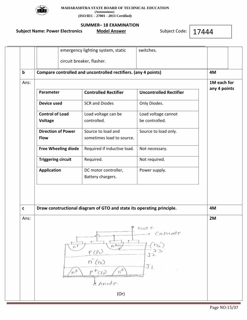
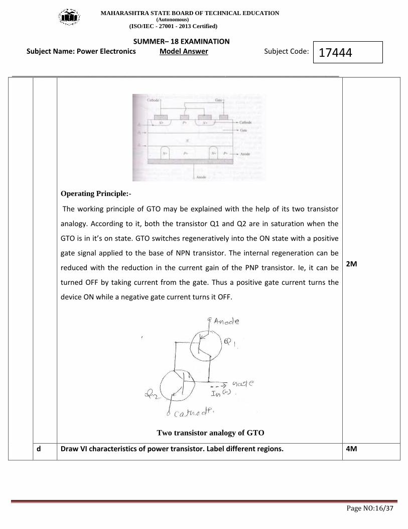
c Draw constructional diagram of GTO and state its operating principle. 4M
Ans:
(Or)
2M
MAHARASHTRA STATE BOARD OF TECHNICAL EDUCATION (Autonomous)
(ISO/IEC - 27001 - 2013 Certified)
SUMMER– 18 EXAMINATION Subject Name: Power Electronics Model Answer Subject Code:
__________________________________________________________________________________________________
Page NO:16/37
17444
Operating Principle:-
The working principle of GTO may be explained with the help of its two transistor
analogy. According to it, both the transistor Q1 and Q2 are in saturation when the
GTO is in it’s on state. GTO switches regeneratively into the ON state with a positive
gate signal applied to the base of NPN transistor. The internal regeneration can be
reduced with the reduction in the current gain of the PNP transistor. Ie, it can be
turned OFF by taking current from the gate. Thus a positive gate current turns the
device ON while a negative gate current turns it OFF.
Two transistor analogy of GTO
2M
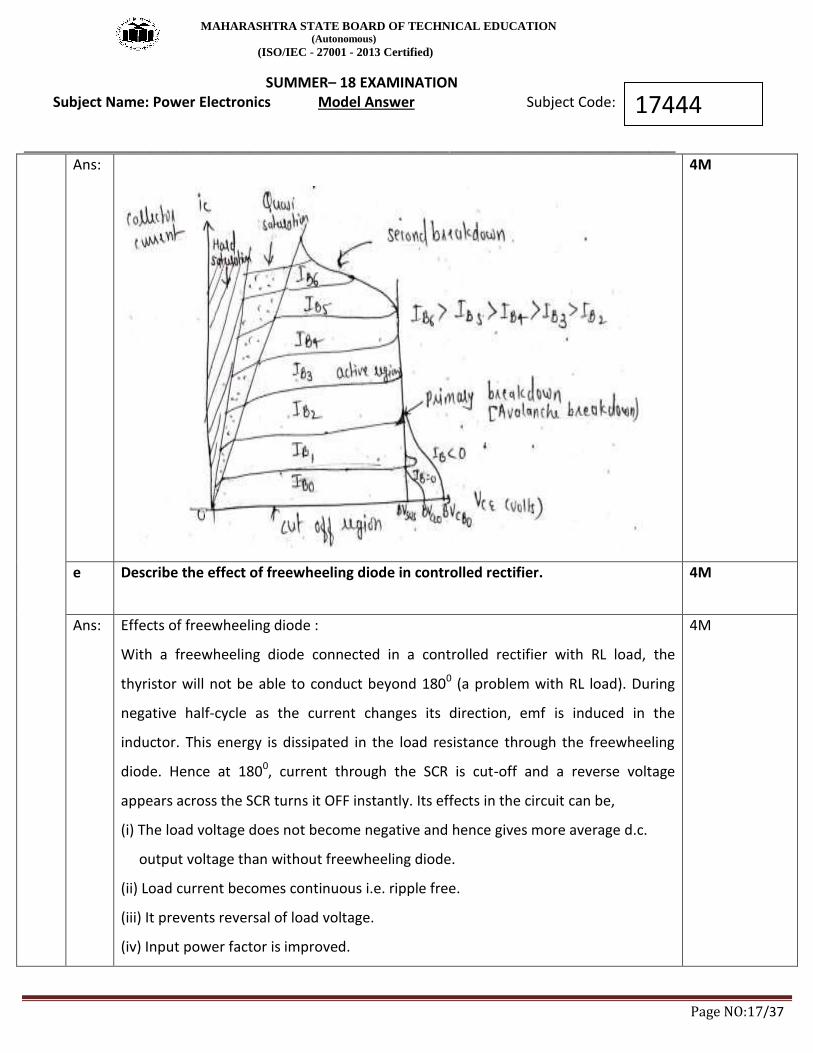
d Draw VI characteristics of power transistor. Label different regions. 4M
MAHARASHTRA STATE BOARD OF TECHNICAL EDUCATION (Autonomous)
(ISO/IEC - 27001 - 2013 Certified)
SUMMER– 18 EXAMINATION Subject Name: Power Electronics Model Answer Subject Code:
__________________________________________________________________________________________________
Page NO:17/37
17444
Ans:
4M
e Describe the effect of freewheeling diode in controlled rectifier.
4M
Ans:
Effects of freewheeling diode :
With a freewheeling diode connected in a controlled rectifier with RL load, the
thyristor will not be able to conduct beyond 1800 (a problem with RL load). During
negative half-cycle as the current changes its direction, emf is induced in the
inductor. This energy is dissipated in the load resistance through the freewheeling
diode. Hence at 1800, current through the SCR is cut-off and a reverse voltage
appears across the SCR turns it OFF instantly. Its effects in the circuit can be,
(i) The load voltage does not become negative and hence gives more average d.c.
output voltage than without freewheeling diode.
(ii) Load current becomes continuous i.e. ripple free.
(iii) It prevents reversal of load voltage.
(iv) Input power factor is improved.
4M
MAHARASHTRA STATE BOARD OF TECHNICAL EDUCATION (Autonomous)
(ISO/IEC - 27001 - 2013 Certified)
SUMMER– 18 EXAMINATION Subject Name: Power Electronics Model Answer Subject Code:
__________________________________________________________________________________________________
Page NO:18/37
17444
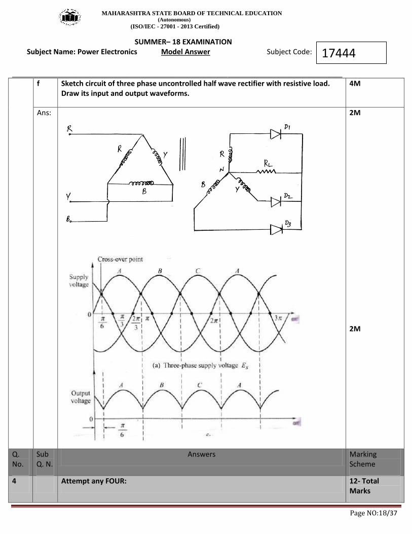
f Sketch circuit of three phase uncontrolled half wave rectifier with resistive load. Draw its input and output waveforms.
4M
Ans:
2M
2M
Q. No.
Sub Q. N.
Answers Marking Scheme
4 Attempt any FOUR: 12- Total Marks
MAHARASHTRA STATE BOARD OF TECHNICAL EDUCATION (Autonomous)
(ISO/IEC - 27001 - 2013 Certified)
SUMMER– 18 EXAMINATION Subject Name: Power Electronics Model Answer Subject Code:
__________________________________________________________________________________________________
Page NO:19/37
17444
a State the need of Inverter. List four applications of Inverters. 4M
Ans:
In most of the industrial applications, inverter is a part of a DC link converter. Its first
stage is a AC to DC rectifier and second DC to AC inverter. In this system the AC
power at line frequency is rectified and filtered and then inverted into AC at an
adjustable voltage and frequency which is required in UPS, low power portable
electronics systems, AC motor speed control etc. so inverter is an essential part of a
two stage static frequency converter.
Applications
Variable speed a c motor drivers
Induction heating
Aircraft power supplies
Uninterrupted power supplies (UPS)
High voltage d c transmission lines
Battery vehicles drives
Regulated voltage and frequency power supplies
2M
2M
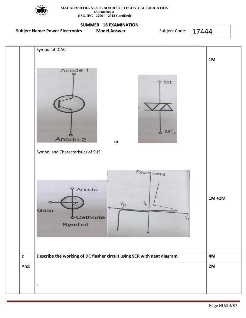
b Draw symbol and characteristics of DIAC and SUS. 4M
Ans:
VI characteristics of DIAC
1M
MAHARASHTRA STATE BOARD OF TECHNICAL EDUCATION (Autonomous)
(ISO/IEC - 27001 - 2013 Certified)
SUMMER– 18 EXAMINATION Subject Name: Power Electronics Model Answer Subject Code:
__________________________________________________________________________________________________
Page NO:20/37
17444
Symbol of DIAC
or
Symbol and Characteristics of SUS
1M
1M +1M
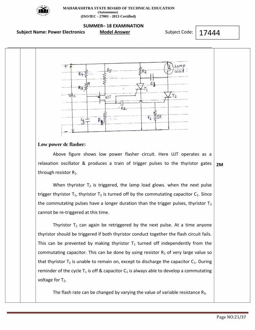
c Describe the working of DC flasher circuit using SCR with neat diagram. 4M
Ans:
‘
2M
MAHARASHTRA STATE BOARD OF TECHNICAL EDUCATION (Autonomous)
(ISO/IEC - 27001 - 2013 Certified)
SUMMER– 18 EXAMINATION Subject Name: Power Electronics Model Answer Subject Code:
__________________________________________________________________________________________________
Page NO:21/37
17444
Low power dc flasher:
Above figure shows low power flasher circuit. Here UJT operates as a
relaxation oscillator & produces a train of trigger pulses to the thyristor gates
through resistor R1.
When thyristor T2 is triggered, the lamp load glows. when the next pulse
trigger thyristor T1, thyristor T2 is turned off by the commutating capacitor C1. Since
the commutating pulses have a longer duration than the trigger pulses, thyristor T2
cannot be re-triggered at this time.
Thyristor T2 can again be retriggered by the next pulse. At a time anyone
thyristor should be triggered if both thyristor conduct together the flash circuit fails.
This can be prevented by making thyristor T1 turned off independently from the
commutating capacitor. This can be done by using resistor R2 of very large value so
that thyristor T2 is unable to remain on, except to discharge the capacitor C1. During
reminder of the cycle T1 is off & capacitor C1 is always able to develop a commutating
voltage for T2.
The flash rate can be changed by varying the value of variable resistance R3.
2M
MAHARASHTRA STATE BOARD OF TECHNICAL EDUCATION (Autonomous)
(ISO/IEC - 27001 - 2013 Certified)
SUMMER– 18 EXAMINATION Subject Name: Power Electronics Model Answer Subject Code:
__________________________________________________________________________________________________
Page NO:22/37
17444
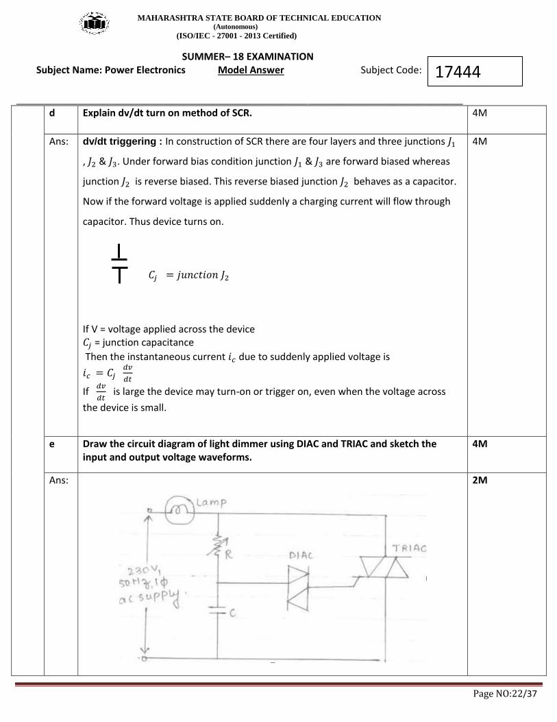
d Explain dv/dt turn on method of SCR. 4M
Ans: dv/dt triggering : In construction of SCR there are four layers and three junctions
, & . Under forward bias condition junction & are forward biased whereas
junction is reverse biased. This reverse biased junction behaves as a capacitor.
Now if the forward voltage is applied suddenly a charging current will flow through
capacitor. Thus device turns on.
If V = voltage applied across the device = junction capacitance
Then the instantaneous current due to suddenly applied voltage is
If
is large the device may turn-on or trigger on, even when the voltage across
the device is small.
4M
e Draw the circuit diagram of light dimmer using DIAC and TRIAC and sketch the input and output voltage waveforms.
4M
Ans:
2M
MAHARASHTRA STATE BOARD OF TECHNICAL EDUCATION (Autonomous)
(ISO/IEC - 27001 - 2013 Certified)
SUMMER– 18 EXAMINATION Subject Name: Power Electronics Model Answer Subject Code:
__________________________________________________________________________________________________
Page NO:23/37
17444
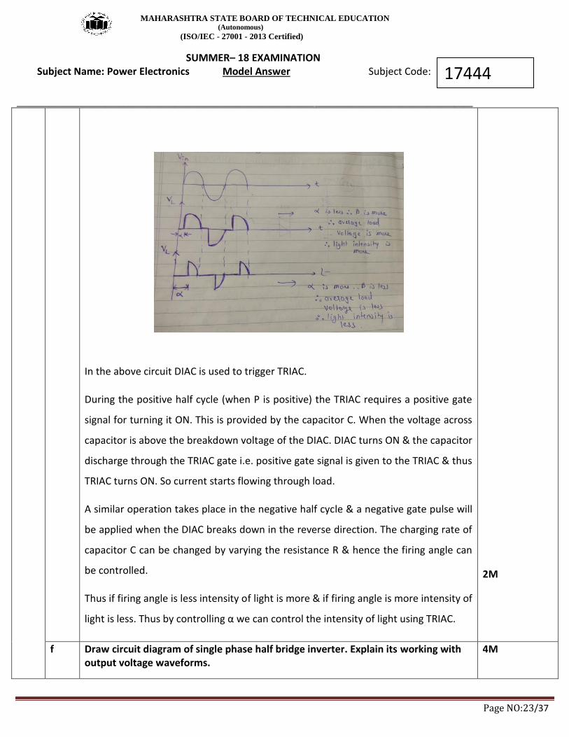
In the above circuit DIAC is used to trigger TRIAC.
During the positive half cycle (when P is positive) the TRIAC requires a positive gate
signal for turning it ON. This is provided by the capacitor C. When the voltage across
capacitor is above the breakdown voltage of the DIAC. DIAC turns ON & the capacitor
discharge through the TRIAC gate i.e. positive gate signal is given to the TRIAC & thus
TRIAC turns ON. So current starts flowing through load.
A similar operation takes place in the negative half cycle & a negative gate pulse will
be applied when the DIAC breaks down in the reverse direction. The charging rate of
capacitor C can be changed by varying the resistance R & hence the firing angle can
be controlled.
Thus if firing angle is less intensity of light is more & if firing angle is more intensity of
light is less. Thus by controlling α we can control the intensity of light using TRIAC.
2M
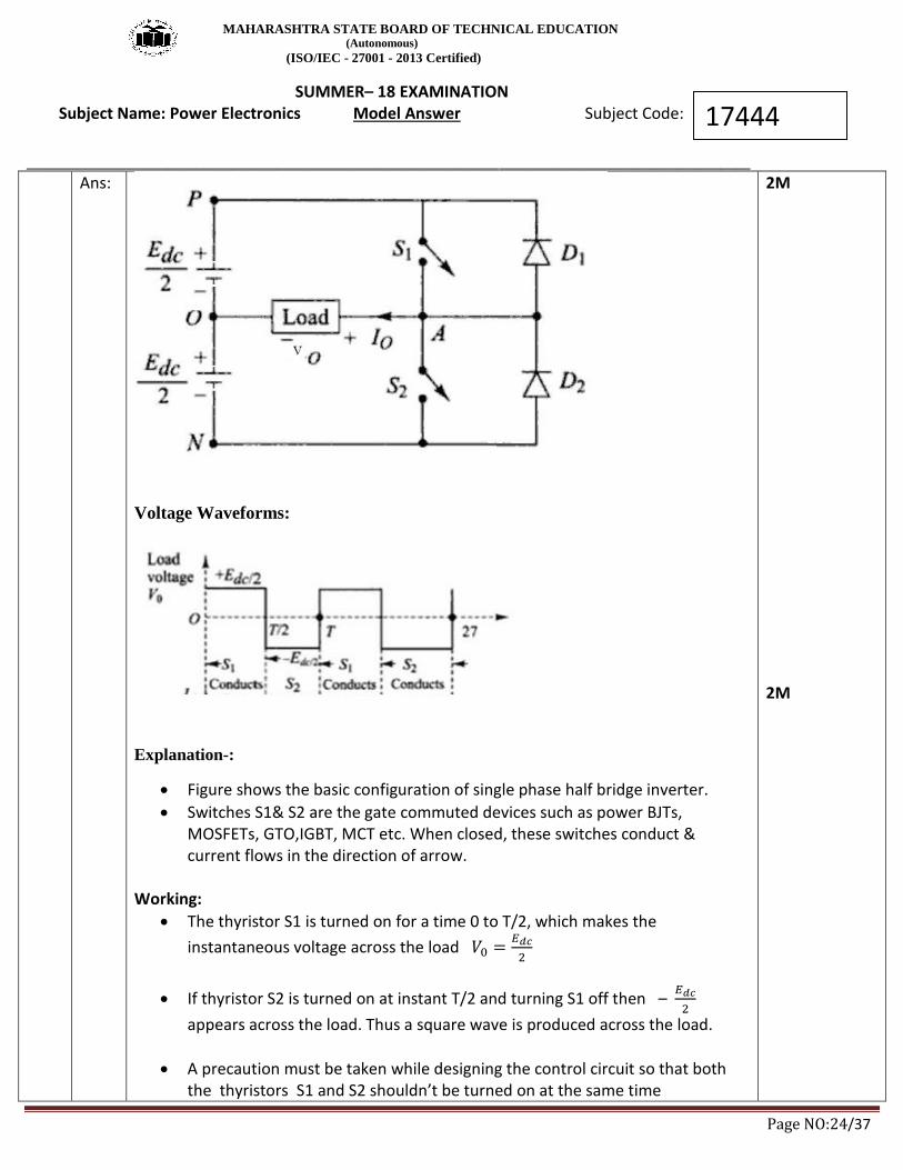
f Draw circuit diagram of single phase half bridge inverter. Explain its working with output voltage waveforms.
4M
MAHARASHTRA STATE BOARD OF TECHNICAL EDUCATION (Autonomous)
(ISO/IEC - 27001 - 2013 Certified)
SUMMER– 18 EXAMINATION Subject Name: Power Electronics Model Answer Subject Code:
__________________________________________________________________________________________________
Page NO:24/37
17444
Ans:
Voltage Waveforms:
Explanation-:
Figure shows the basic configuration of single phase half bridge inverter.
Switches S1& S2 are the gate commuted devices such as power BJTs, MOSFETs, GTO,IGBT, MCT etc. When closed, these switches conduct & current flows in the direction of arrow.
Working:
The thyristor S1 is turned on for a time 0 to T/2, which makes the
instantaneous voltage across the load
If thyristor S2 is turned on at instant T/2 and turning S1 off then –
appears across the load. Thus a square wave is produced across the load.
A precaution must be taken while designing the control circuit so that both the thyristors S1 and S2 shouldn’t be turned on at the same time
2M
2M
MAHARASHTRA STATE BOARD OF TECHNICAL EDUCATION (Autonomous)
(ISO/IEC - 27001 - 2013 Certified)
SUMMER– 18 EXAMINATION Subject Name: Power Electronics Model Answer Subject Code:
__________________________________________________________________________________________________
Page NO:25/37
17444
Diodes D1 and D2 which are connected parallel carry negative current for inductive loads
Simply by controlling the time periods of the on time of thyristor S1 & S2, the frequency can be varied.
Q. No.
Sub Q. N.
Answers Marking Scheme
5 Attempt any FOUR: 16- Total Marks
a Draw labelled circuit diagram of battery charger using SCR. 4M
Ans: circuit diagram (Any relevant diagram can be considered)
4M
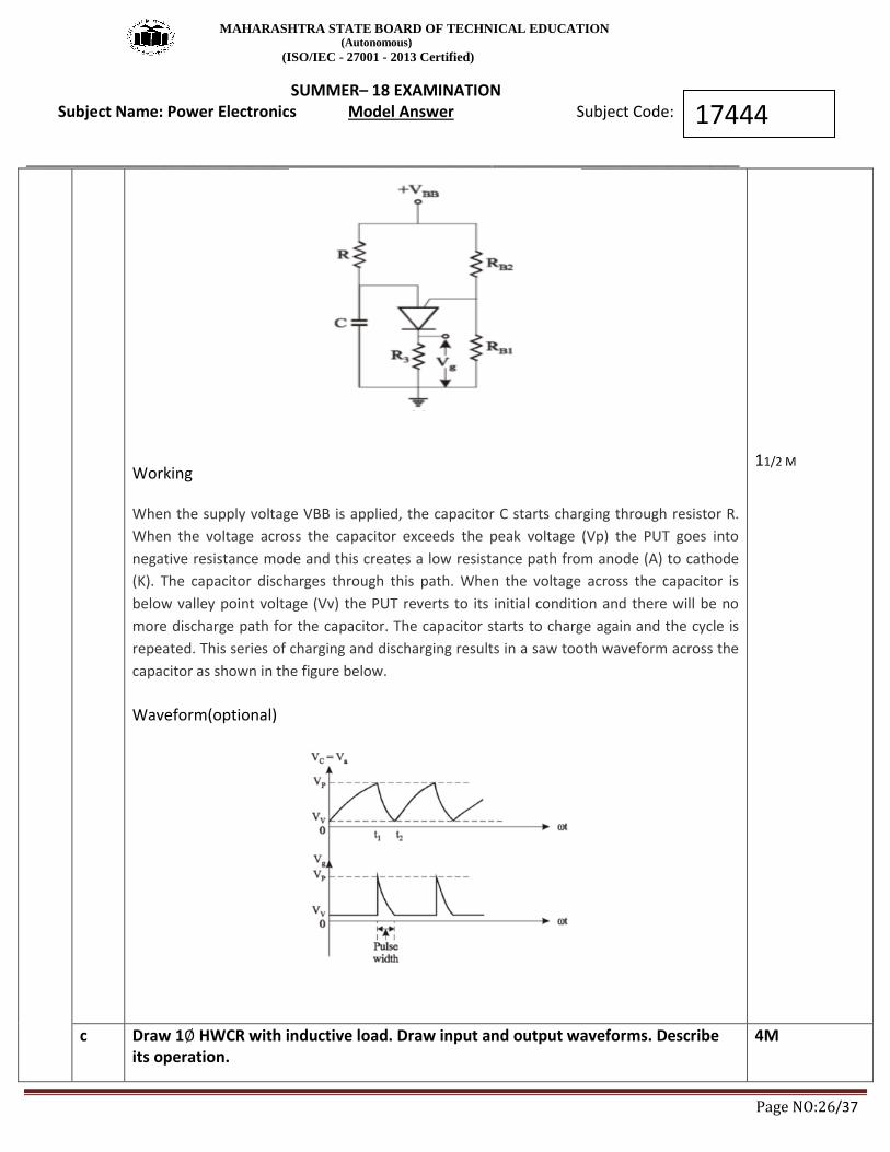
b Draw the layer diagram of PUT. With neat circuit diagram, describe its working as relaxation oscillator.
4M
Ans: layer diagram of PUT
circuit diagram: PUT relaxation oscillator
1M
11/2 M
MAHARASHTRA STATE BOARD OF TECHNICAL EDUCATION (Autonomous)
(ISO/IEC - 27001 - 2013 Certified)
SUMMER– 18 EXAMINATION Subject Name: Power Electronics Model Answer Subject Code:
__________________________________________________________________________________________________
Page NO:26/37
17444
Working
When the supply voltage VBB is applied, the capacitor C starts charging through resistor R.
When the voltage across the capacitor exceeds the peak voltage (Vp) the PUT goes into
negative resistance mode and this creates a low resistance path from anode (A) to cathode
(K). The capacitor discharges through this path. When the voltage across the capacitor is
below valley point voltage (Vv) the PUT reverts to its initial condition and there will be no
more discharge path for the capacitor. The capacitor starts to charge again and the cycle is
repeated. This series of charging and discharging results in a saw tooth waveform across the
capacitor as shown in the figure below.
Waveform(optional)
11/2 M
c Draw 1 HWCR with inductive load. Draw input and output waveforms. Describe its operation.
4M
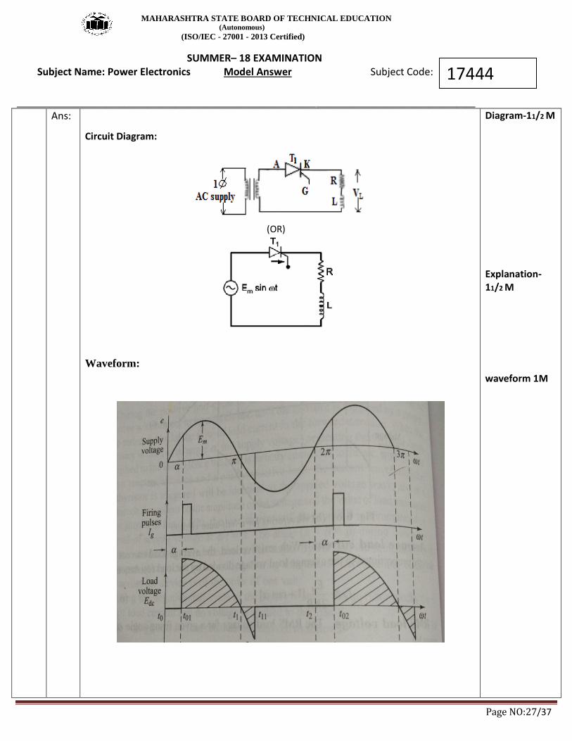
MAHARASHTRA STATE BOARD OF TECHNICAL EDUCATION (Autonomous)
(ISO/IEC - 27001 - 2013 Certified)
SUMMER– 18 EXAMINATION Subject Name: Power Electronics Model Answer Subject Code:
__________________________________________________________________________________________________
Page NO:27/37
17444
Ans:
Circuit Diagram:
(OR)
Waveform:
Diagram-11/2 M
Explanation-11/2 M
waveform 1M
MAHARASHTRA STATE BOARD OF TECHNICAL EDUCATION (Autonomous)
(ISO/IEC - 27001 - 2013 Certified)
SUMMER– 18 EXAMINATION Subject Name: Power Electronics Model Answer Subject Code:
__________________________________________________________________________________________________
Page NO:28/37
17444
Operation:( give marks for correct brief explanation)
Mode 1: (0 to α) (+ve half cycle)
SCR anode is a positive w.r.t. cathode but gate pulse is not applied therefore SCR is in
off state though it is in forward biased therefore load current is zero therefore load
voltage is 0.
Mode 2: (α to π) (+ve half cycle + gate signal is applied)
SCR is forward bias and gate signal is applied therefore SCR turns on at α. When SCR
is triggered the load current will increase in a finite time through the inductive load.
The supplier voltage from this instant appears across the load. Due to the inductive
load the increase in current is gradual, energy is stored in inductor during α to π .
Mode3: (π to 2 π) (negative half cycle) During negative half cycle, current continues
to flow till the energy stored in the inductance is dissipated in the load-register and a
part of the energy is feedback to the source, Hence due to energy stored in inductor,
current continues to flow up to instant t1.at a capital at instant t1 is load current is
zero and due to negative supply voltage SCR turns off. At instant 2 π+ α , when again
pulse is applied the above cycle repeats. Hence the effect of the inductive load is
increase.in the conduction period.
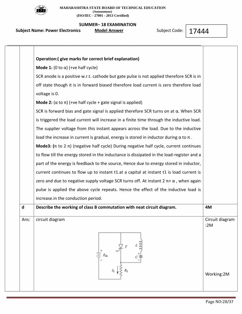
d Describe the working of class B commutation with neat circuit diagram. 4M
Ans: circuit diagram
Circuit diagram :2M
Working:2M
MAHARASHTRA STATE BOARD OF TECHNICAL EDUCATION (Autonomous)
(ISO/IEC - 27001 - 2013 Certified)
SUMMER– 18 EXAMINATION Subject Name: Power Electronics Model Answer Subject Code:
__________________________________________________________________________________________________
Page NO:29/37
17444
Working: 1. As soon as the supply voltage Edc is applied capacitor C charges upto Edc( with upper terminal +ve) 2. When the SCR is triggered, along with load current IL, capacitor current IC flows through thyristor and L,C components, transferring the energy from capacitor to inductor. 3. When completely discharged, C gets charged by the inductor with opposite polarity. This reverse voltage causes a commutating current opposite to that of the load current. 4. When IC increases above the holding current, the SCR turns OFF. 5. AS SCR is turned OFF, capacitor again charges with original polarity through L & RL and the cycle repeats. Waveform( Optional)
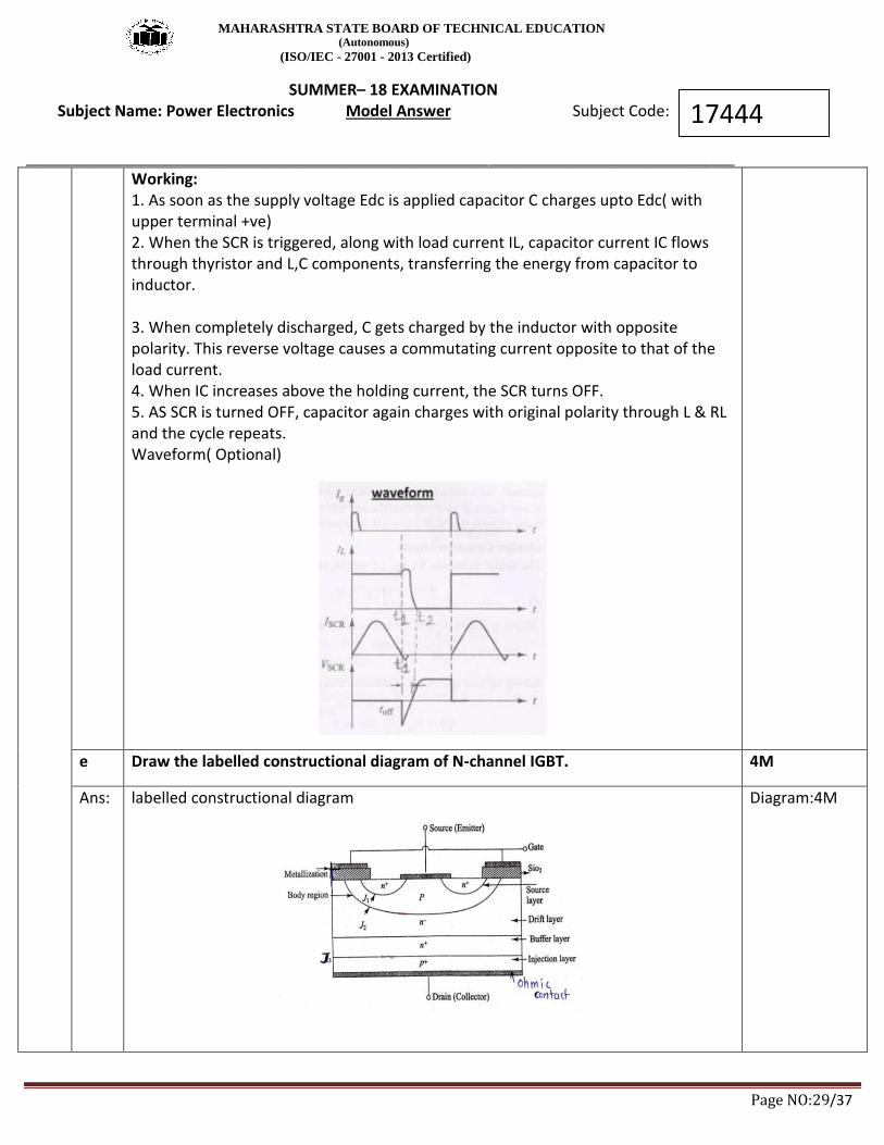
e Draw the labelled constructional diagram of N-channel IGBT. 4M
Ans:
labelled constructional diagram
Diagram:4M
MAHARASHTRA STATE BOARD OF TECHNICAL EDUCATION (Autonomous)
(ISO/IEC - 27001 - 2013 Certified)
SUMMER– 18 EXAMINATION Subject Name: Power Electronics Model Answer Subject Code:
__________________________________________________________________________________________________
Page NO:30/37
17444
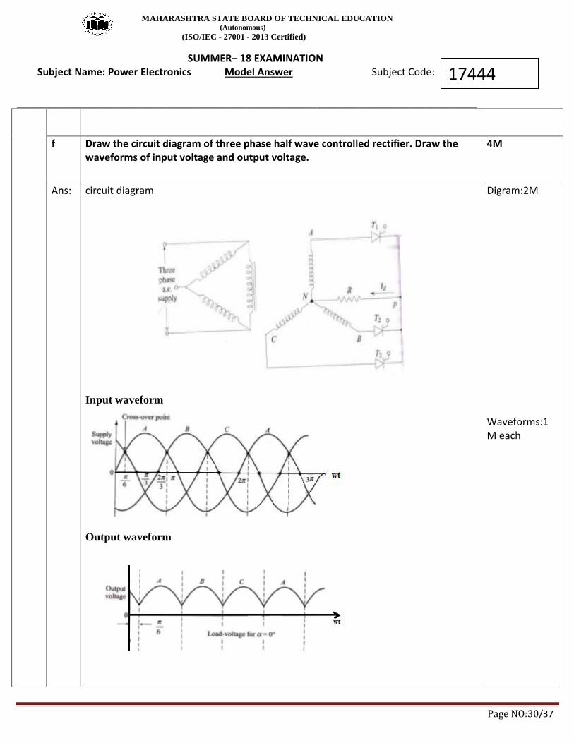
f Draw the circuit diagram of three phase half wave controlled rectifier. Draw the waveforms of input voltage and output voltage.
4M
Ans:
circuit diagram
Input waveform
Output waveform
Digram:2M
Waveforms:1M each
MAHARASHTRA STATE BOARD OF TECHNICAL EDUCATION (Autonomous)
(ISO/IEC - 27001 - 2013 Certified)
SUMMER– 18 EXAMINATION Subject Name: Power Electronics Model Answer Subject Code:
__________________________________________________________________________________________________
Page NO:31/37
17444
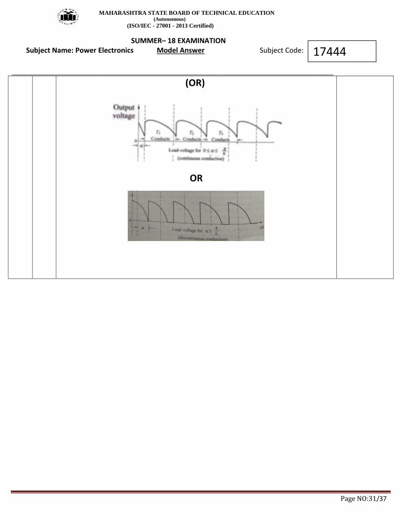
(OR)
OR
MAHARASHTRA STATE BOARD OF TECHNICAL EDUCATION (Autonomous)
(ISO/IEC - 27001 - 2013 Certified)
SUMMER– 18 EXAMINATION Subject Name: Power Electronics Model Answer Subject Code:
__________________________________________________________________________________________________
Page NO:32/37
17444
Q. No.
Sub Q. N.
Answers Marking Scheme
6 Attempt any FOUR: 16- Total Marks
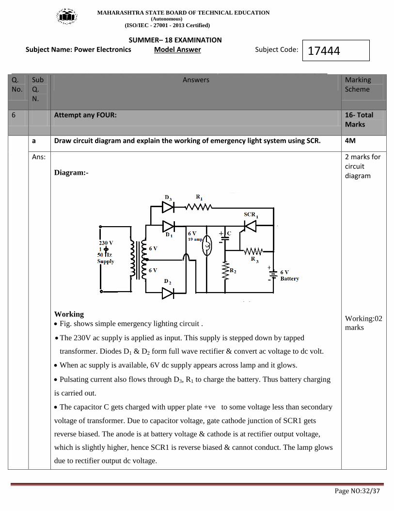
a Draw circuit diagram and explain the working of emergency light system using SCR. 4M
Ans:
Diagram:-
Working
Fig. shows simple emergency lighting circuit .
The 230V ac supply is applied as input. This supply is stepped down by tapped
transformer. Diodes D1 & D2 form full wave rectifier & convert ac voltage to dc volt.
When ac supply is available, 6V dc supply appears across lamp and it glows.
Pulsating current also flows through D3, R1 to charge the battery. Thus battery charging
is carried out.
The capacitor C gets charged with upper plate +ve to some voltage less than secondary
voltage of transformer. Due to capacitor voltage, gate cathode junction of SCR1 gets
reverse biased. The anode is at battery voltage & cathode is at rectifier output voltage,
which is slightly higher, hence SCR1 is reverse biased & cannot conduct. The lamp glows
due to rectifier output dc voltage.
2 marks for circuit diagram
Working:02
marks
MAHARASHTRA STATE BOARD OF TECHNICAL EDUCATION (Autonomous)
(ISO/IEC - 27001 - 2013 Certified)
SUMMER– 18 EXAMINATION Subject Name: Power Electronics Model Answer Subject Code:
__________________________________________________________________________________________________
Page NO:33/37
17444
If power fails, the capacitor C discharges through D3,R1 & R3 until the cathode of SCR1
is less positive than anode. At the same time the junction of R2 & R3 becomes +ve &
establishes a sufficient gate to cathode voltage to trigger the thyristor. Once the thyristor
turns ON, the battery discharges through it, & turns the lamp ON when power is restored,
the thyristor is commutated & capacitor C is recharged again.
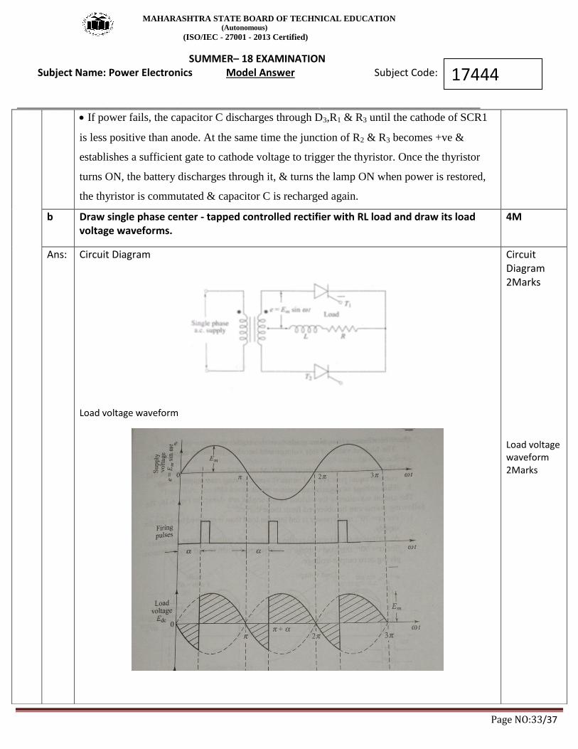
b Draw single phase center - tapped controlled rectifier with RL load and draw its load voltage waveforms.
4M
Ans: Circuit Diagram
Load voltage waveform
Circuit Diagram 2Marks
Load voltage waveform 2Marks
MAHARASHTRA STATE BOARD OF TECHNICAL EDUCATION (Autonomous)
(ISO/IEC - 27001 - 2013 Certified)
SUMMER– 18 EXAMINATION Subject Name: Power Electronics Model Answer Subject Code:
__________________________________________________________________________________________________
Page NO:34/37
17444
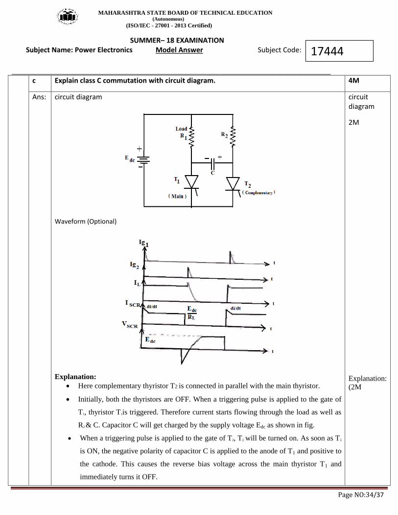
c Explain class C commutation with circuit diagram. 4M
Ans: circuit diagram
Waveform (Optional)
Explanation:
Here complementary thyristor T2 is connected in parallel with the main thyristor.
Initially, both the thyristors are OFF. When a triggering pulse is applied to the gate of
T1, thyristor T1is triggered. Therefore current starts flowing through the load as well as
R2 & C. Capacitor C will get charged by the supply voltage Edc as shown in fig.
When a triggering pulse is applied to the gate of T2, T2 will be turned on. As soon as T2
is ON, the negative polarity of capacitor C is applied to the anode of T1 and positive to
the cathode. This causes the reverse bias voltage across the main thyristor T1 and
immediately turns it OFF.
circuit diagram
2M
Explanation:
(2M
MAHARASHTRA STATE BOARD OF TECHNICAL EDUCATION (Autonomous)
(ISO/IEC - 27001 - 2013 Certified)
SUMMER– 18 EXAMINATION Subject Name: Power Electronics Model Answer Subject Code:
__________________________________________________________________________________________________
Page NO:35/37
17444
d State two applications each for (i) SCR and (ii) PUT. 4M
Ans: Applications of SCR:
1. Controlled rectifier
2. Choppers
3. Inverters
4. High voltage DC transmission system
5. Battery charger circuit
6. Dc drivers
7. Subway cars
8. SMPS
9. UPS
10. Emergency lighting system
11. Electronic timer
12. Temperature controller
Applications of PUT:
1. Time delay circuit
2. Logic circuit
3. SCR trigger circuit
2Marks for
any two
applications
2Marks for
any two
applications
e Explain the secondary breakdown in power BJT and how it can be avoided? 4M
Ans:
Second Breakdown in Power BJT:
In the active region the ratio of collector current to base current (DC current gain (β))
remains fairly constant up to certain value of the collector current after which it falls of
rapidly. At still higher levels of collector currents the allowable active region is further
restricted by a potential failure mode call “the second breakdown”. It appears on the o/p
characteristics of the BJT as a precipitous drop in the collector emitter voltage at large
collector currents. The collector voltage drop is often accompanied by significant rise in
the collector current & a substantial increase in the power dissipation. Most importantly
this dissipation is not uniformly spread over the entire volume of the device but is
concentrated in highly localized regions. This localized heating is a combined effect of the
intrinsic non uniformity of the collector current density distribution across the cross section
of the device & the negative temperature coefficient of resistivity of minority carrier device
which leads to the formation of “current filaments” (localized across of very high current
2Marks for secondary breakdown in power BJT
MAHARASHTRA STATE BOARD OF TECHNICAL EDUCATION (Autonomous)
(ISO/IEC - 27001 - 2013 Certified)
SUMMER– 18 EXAMINATION Subject Name: Power Electronics Model Answer Subject Code:
__________________________________________________________________________________________________
Page NO:36/37
17444
density) by a positive feedback mechanism.
Once current filaments are formed, localized “thermal runaway” quickly takes the junction
temperature beyond the safe limit & the device is destroyed.
How to avoid secondary breakdown:
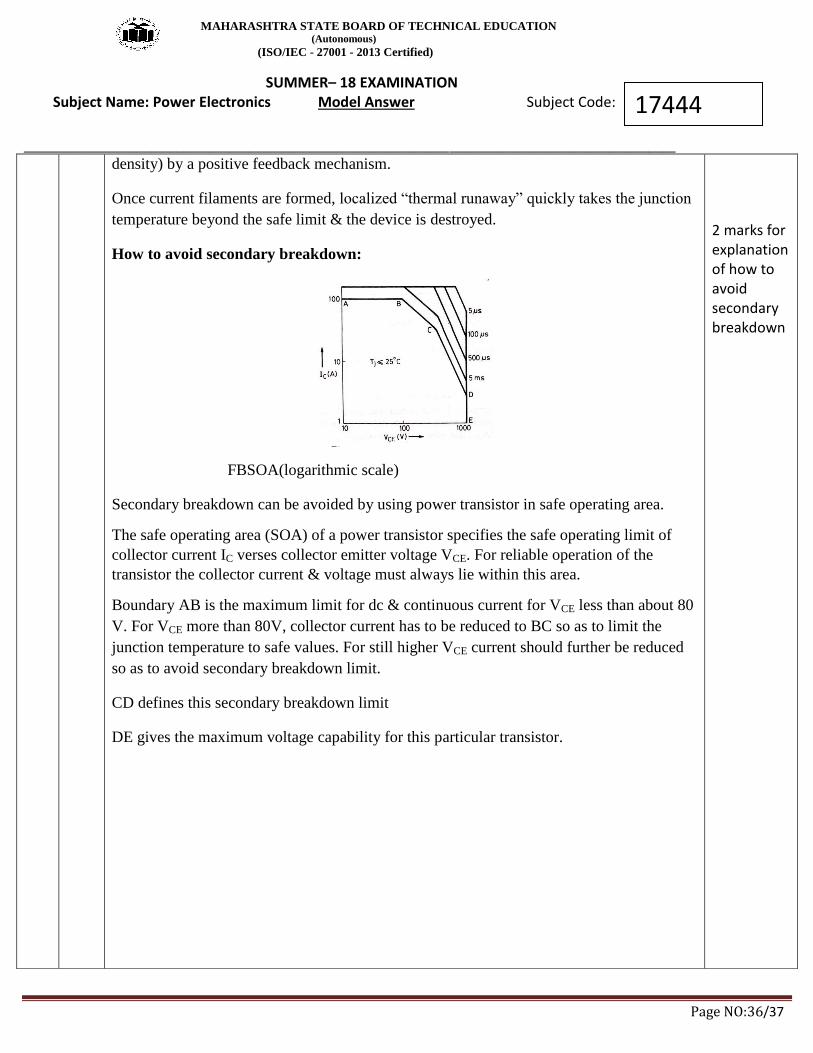
FBSOA(logarithmic scale)
Secondary breakdown can be avoided by using power transistor in safe operating area.
The safe operating area (SOA) of a power transistor specifies the safe operating limit of
collector current IC verses collector emitter voltage VCE. For reliable operation of the
transistor the collector current & voltage must always lie within this area.
Boundary AB is the maximum limit for dc & continuous current for VCE less than about 80
V. For VCE more than 80V, collector current has to be reduced to BC so as to limit the
junction temperature to safe values. For still higher VCE current should further be reduced
so as to avoid secondary breakdown limit.
CD defines this secondary breakdown limit
DE gives the maximum voltage capability for this particular transistor.
2 marks for explanation of how to avoid secondary breakdown
MAHARASHTRA STATE BOARD OF TECHNICAL EDUCATION (Autonomous)
(ISO/IEC - 27001 - 2013 Certified)
SUMMER– 18 EXAMINATION Subject Name: Power Electronics Model Answer Subject Code:
__________________________________________________________________________________________________
Page NO:37/37
17444
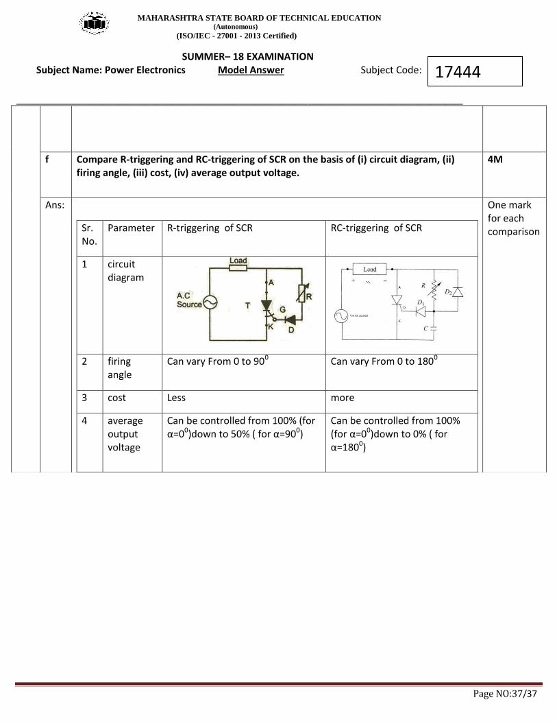
f Compare R-triggering and RC-triggering of SCR on the basis of (i) circuit diagram, (ii) firing angle, (iii) cost, (iv) average output voltage.
4M
Ans:
Sr. No.
Parameter R-triggering of SCR RC-triggering of SCR
1 circuit diagram
2 firing angle
Can vary From 0 to 900 Can vary From 0 to 1800
3 cost Less more
4 average output voltage
Can be controlled from 100% (for α=00)down to 50% ( for α=900)
Can be controlled from 100% (for α=00)down to 0% ( for α=1800)
One mark for each comparison