Embed Size (px)
Citation preview

Case Study: For academic or private use only; all rights reserved
Wolfgang Runge 1 of 53
August 2014
Supplement to the Treatise
WOLFGANG RUNGE: TECHNOLOGY ENTREPRENEURSHIP How to access the treatise is given at the end of this document.
Reference to this treatise will be made in the following form: [Runge:page number(s), chapters (A.1.1) or other chunks, such as tables or figures].
The current case relates to a group of German university spin-outs or research-based startups (RBSUs), respectively, based on scientific optical instruments and specifically nanotools, WITec GmbH, JPK Instruments AG, and Attocube Systems AG for which individual case documents are generated. All university startups are more or less competitors, but exhibit different paths of development which represents a “science2business” approach.
This cluster of startups deals with an enabling technology for nanotechnology, very highly re-solved microscopy, which was honored with the Nobel Prize in Chemistry 2014 awarded jointly to William E. Moerner, Eric Betzig, both from the US and Stefan W. Hell (Germany) “for the development of super-resolved fluorescence microscopy."
In this context the current case provides information on technology and markets as well as competitive situations for all the other two startups.
Wolfgang Runge
WITec GmbH Table of Contents The Technology and the Market ................................................................................................ 2
Awards and Publicity ................................................................................................................. 8
The Entrepreneurs ..................................................................................................................... 9
Business Idea, Opportunity, Foundation and Product Developments..................................... 12
Financing, Networking, and Organization ............................................................................ 17
Innovation Persistence, Expansion and Diversification ........................................................... 23
Key Metrics .............................................................................................................................. 27
Intellectual Properties .............................................................................................................. 28
Vision/Mission, Business Model and Risks ............................................................................. 31
Probe Microscopy and the Related Instrumental Community ................................................. 37
Competition .............................................................................................................................. 39
References .............................................................................................................................. 45
Notes ....................................................................................................................................... 52

Case Study: For academic or private use only; all rights reserved
Wolfgang Runge 2 of 53
WITec (Wissenschaftliche Instrumente und Technologie) GmbH is a spin-out of the Department of Experimental Physics of the University of Ulm (Germany) and was founded in 1997 by three colleagues from the department – an entrepreneurial triple [Runge:191,306,328]. After plans to found a firm in the IT-sector they grasped an opportunity in scientific instruments, in their field of expertise.
After more than fifteen years of existence WITec has become an established global player in high-tech instrumentation, essentially in the area of nanotools.
Nanoscience deals with tools, methods, phenomena and techniques leading to a deeper under-standing of nanoscale properties. Nanotools cover production and test equipment as well as analytical equipment for the fabrication and characterization of structures in the nanometer range (1 nm = 10-9 meter, one billionth of a meter) or which work with nanometer precision or resolution. They are focused on measurement or (atomic and molecular) manipulation devices, such as nanopositioners for moving atoms. Nanotools represent enabling technologies [Runge:129, Table I.12].
WITec represents an example of developing technology from purely research tools to work in science and large-scale production processes.
By its own account, WITec GmbH is one of the world's leading manufacturers of high-resolution optical and scanning probe microscopes (SPMs), a market leader in the field of nanoanalytical microscope systems.
A modular product line allows the combination of different microscopy techniques, such as Raman, Scanning Near-Field Optical Microscopy (SNOM, sometimes abbreviated by NSOM) using unique cantilever technology and Atomic Force Microscopes (AFMs), in one instrument, allowing for comprehensive flexible chemical, structural and optical analysis of a sample. The high-powered microscope systems are sold worldwide and used primarily in the fields of semiconductors, materials science, life science and nanotechnology.
The Technology and the Market Nanotechnology focuses in particular on nanoscale properties and effects of bulk material and surfaces, and on miniaturization of technical equipment providing new and unique kinds of ap-plications. Nanomaterials and nanotools are clearly the areas that are currently most developed in the nanotechnology arena.
Around 2,000 governmental organizations all over the world provide strategic (financial) support of nanotechnology-related research and development. The results of related research and de-velopment projects in nanomaterials and nanotools were expected to contribute to creation and advancement of new visualization and measurement equipment as well as tools for manipula-tion and positioning of atoms or molecules on the nano-level.
Since the market is barely controlled by any regulations and laws to note, it can be said that the obstacles for foreign manufacturers in entering the home market and other markets abroad are rather small.
In the area of analytical instruments and spectroscopy they are used for natural sciences and life sciences research, lab testing and quality control and other scientific and industrial ap-plications. Special analytical instruments comprise X-ray diffraction, electron microscopy, liquid chromatography, Scanning Probe Microscopes (SPMs; Rastersondenmikroskope), and Atomic Force Microscopes (AFMs; atomare Kraftmikroskope or Raster-Kraftmikroskope).
The atomic-force microscope "is the granddaddy of nanotechnology tools." Scanning probe microscopy (SPM) allows to directly observe atoms and molecules as discrete components rather than as an average provided by traditional analytical methods.
Case Study: For academic or private use only; all rights reserved
Wolfgang Runge 3 of 53
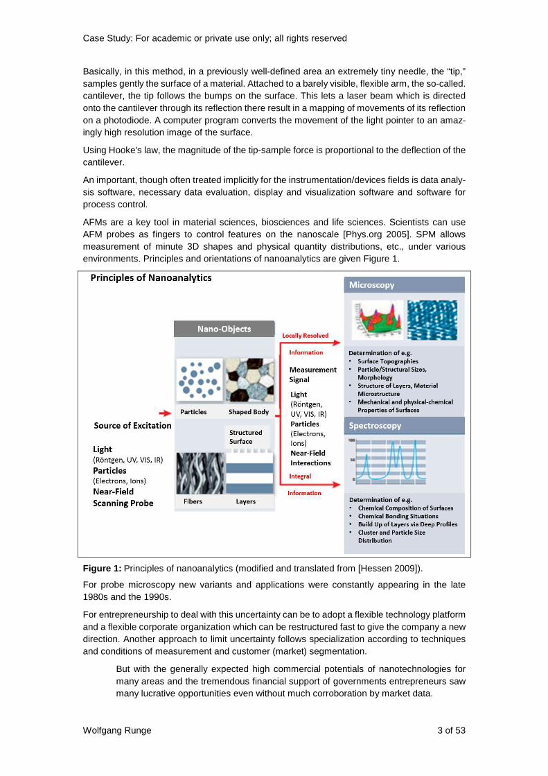
Basically, in this method, in a previously well-defined area an extremely tiny needle, the “tip,” samples gently the surface of a material. Attached to a barely visible, flexible arm, the so-called. cantilever, the tip follows the bumps on the surface. This lets a laser beam which is directed onto the cantilever through its reflection there result in a mapping of movements of its reflection on a photodiode. A computer program converts the movement of the light pointer to an amaz-ingly high resolution image of the surface.
Using Hooke's law, the magnitude of the tip-sample force is proportional to the deflection of the cantilever.
An important, though often treated implicitly for the instrumentation/devices fields is data analy-sis software, necessary data evaluation, display and visualization software and software for process control.
AFMs are a key tool in material sciences, biosciences and life sciences. Scientists can use AFM probes as fingers to control features on the nanoscale [Phys.org 2005]. SPM allows measurement of minute 3D shapes and physical quantity distributions, etc., under various environments. Principles and orientations of nanoanalytics are given Figure 1.
Figure 1: Principles of nanoanalytics (modified and translated from [Hessen 2009]).
For probe microscopy new variants and applications were constantly appearing in the late 1980s and the 1990s.
For entrepreneurship to deal with this uncertainty can be to adopt a flexible technology platform and a flexible corporate organization which can be restructured fast to give the company a new direction. Another approach to limit uncertainty follows specialization according to techniques and conditions of measurement and customer (market) segmentation.
But with the generally expected high commercial potentials of nanotechnologies for many areas and the tremendous financial support of governments entrepreneurs saw many lucrative opportunities even without much corroboration by market data.
Case Study: For academic or private use only; all rights reserved
Wolfgang Runge 4 of 53
Business and market considerations published during the early phase of WITec
“Analytical Instruments Industry Report put the SPM market at $150-$170 million in 2001, with expectations to double.” [Jamison 2003]
The super-ordinate global market for nanophotonic devices was projected to rise at an average annual growth rate (AAGR) of 85.8 percent from $420.7 million in 2004 to $9.325 billion in 2009. Near-field optics were assumed to account for 18.7 percent – approximately with $1.7 billion in 2009 [The Info Shop [2005].
In 2005 it was expected that instruments and tools are needed to work on the nanoscale. Even when excluding the semiconductor industry, they will form a $700 million market by 2008. A growing market within nanotechnology tools was seen for accessories to existing AFMs and other “workhorse machines.” “These are probes or tips that you stick on the end of a microscope that can do whatever you want them to." "There are a lot of smart entrepreneurs and scientists who are developing more and more advanced accessories to add onto standardized scopes as you get more and more specialized applications.” [Phys.org 2005]
A detailed report dealing with “Nanoscale Equipment for Visualization and Measurement” for the period 2003-2005 for Japan and the global situation [JETRO 2006] tackled among others the following categories of current interest:
• Scanning probe microscope (SPM) • Scanning Near-Field Optical Microscope (SNOM) • Micro Raman measurement system • Data analysis software.
To convert data in Japanese Yen into dollar we shall use an average of 1 dollar = 117 Yen for the whole period [Wikipedia-1].
It was estimated [JETRO 2006] that the market of nanoscale equipment for visualization and measurement in the world reached to 160 billion yen ($1.37 billion) or above in 2004, a third (33.8 percent) of which was occupied by the demand from the Japanese market. Japan was considered as the second largest market in the world next to the US.
The boom of the Japanese market in this business sector was attributed to the demand of this equipment by semiconductor, electronic parts and devices sectors and strategic support from the Japanese Government toward nanotechnology-related research and development.
The sub-markets of data analysis software and micro Raman measurement systems were inter-esting markets in terms of high growth, though their market shares in the world were slightly less than the above products.
A summary of the situation in given in Table 1, a description of the related technologies in Table 2. Basic principles of all SPM techniques are based upon scanning a probe using a tip just above a surface whilst monitoring some interaction between the probe and the surface.
Further descriptions of the considered technologies are given by Koenen [2010] and NT-MDT [2010]. Near-field interaction [Koenen 2010:15-18] probe optical interactions of a sample, dis-tant from the source of an aperture, by a fraction of the wavelength of light. It forms the basis for near-field scanning optical microscopy (SNOM).
• SNOM provides an imaging resolution of ≤100 nm, which is significantly better than the diffraction limit imposed in a classical microscope.
• The two approaches used for implementing SNOM are: 1) passing light through a sub-wavelength aperture, also known as aperture SNOM, and 2) localization and field enhancement around a metallic nanoparticle or a metallic tip, which is called aper-tureless SNOM.
Case Study: For academic or private use only; all rights reserved
Wolfgang Runge 5 of 53
There is a number of theoretical methods available to model the near-field distribution of the electromagnetic field.
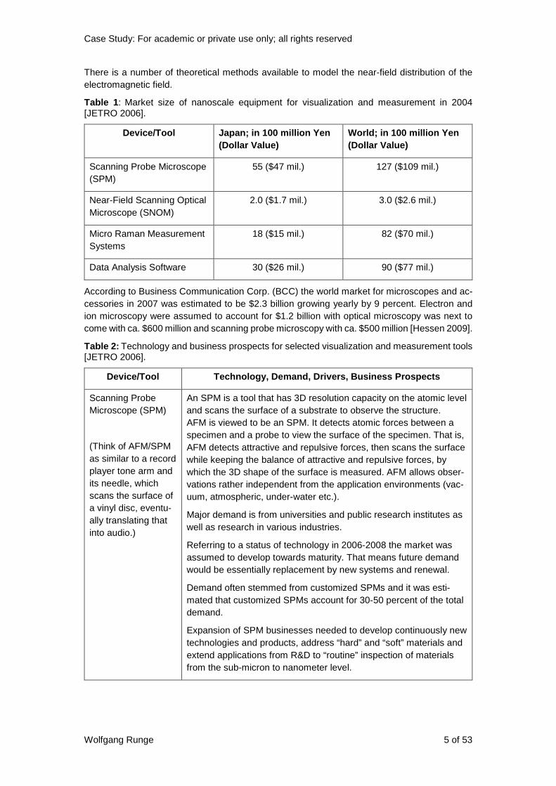
Table 1 : Market size of nanoscale equipment for visualization and measurement in 2004 [JETRO 2006].
Device/Tool Japan; in 100 million Yen (Dollar Value)
World; in 100 million Yen (Dollar Value)
Scanning Probe Microscope (SPM)
55 ($47 mil.) 127 ($109 mil.)
Near-Field Scanning Optical Microscope (SNOM)
2.0 ($1.7 mil.) 3.0 ($2.6 mil.)
Micro Raman Measurement Systems
18 ($15 mil.) 82 ($70 mil.)
Data Analysis Software 30 ($26 mil.) 90 ($77 mil.)
According to Business Communication Corp. (BCC) the world market for microscopes and ac-cessories in 2007 was estimated to be $2.3 billion growing yearly by 9 percent. Electron and ion microscopy were assumed to account for $1.2 billion with optical microscopy was next to come with ca. $600 million and scanning probe microscopy with ca. $500 million [Hessen 2009].
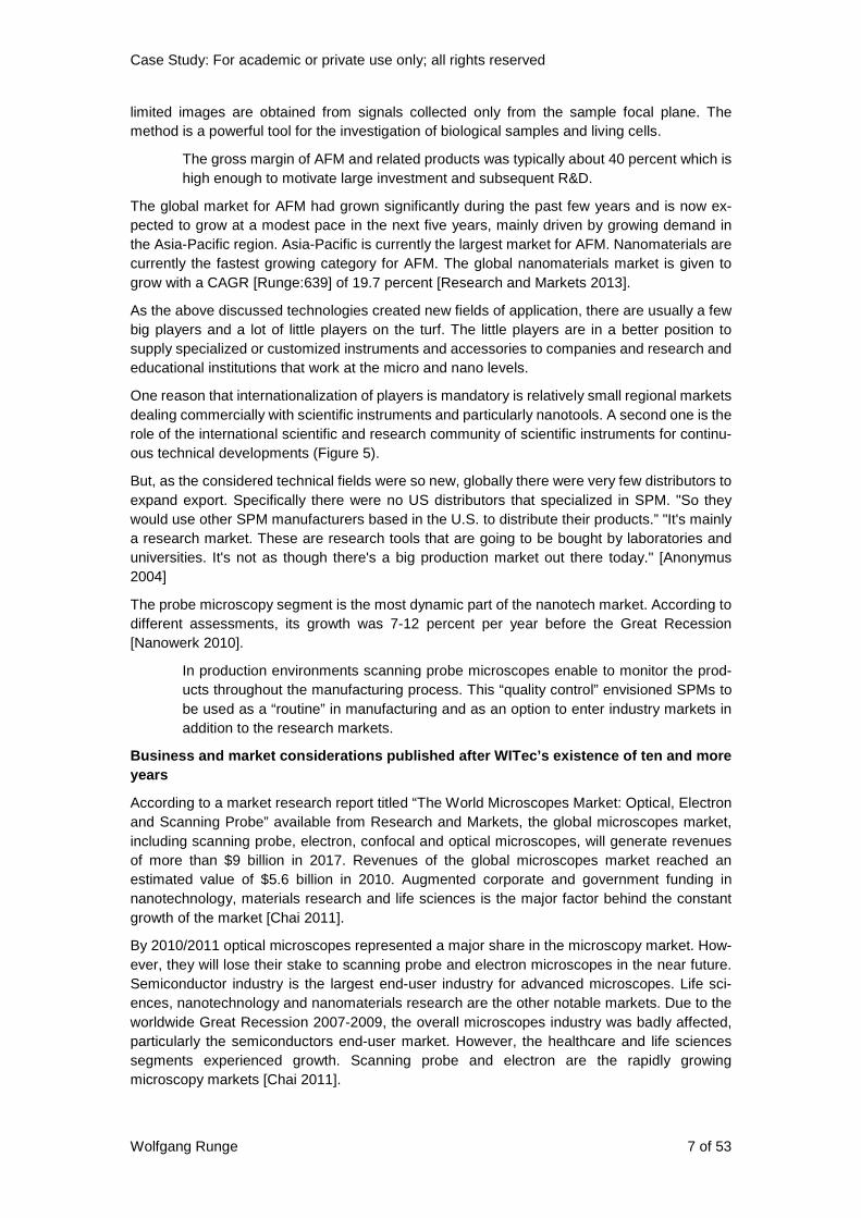
Table 2: Technology and business prospects for selected visualization and measurement tools [JETRO 2006].
Device/Tool Technology, Demand, Drivers, Business P rospects
Scanning Probe Microscope (SPM)
(Think of AFM/SPM as similar to a record player tone arm and its needle, which scans the surface of a vinyl disc, eventu-ally translating that into audio.)
An SPM is a tool that has 3D resolution capacity on the atomic level and scans the surface of a substrate to observe the structure. AFM is viewed to be an SPM. It detects atomic forces between a specimen and a probe to view the surface of the specimen. That is, AFM detects attractive and repulsive forces, then scans the surface while keeping the balance of attractive and repulsive forces, by which the 3D shape of the surface is measured. AFM allows obser-vations rather independent from the application environments (vac-uum, atmospheric, under-water etc.).
Major demand is from universities and public research institutes as well as research in various industries.
Referring to a status of technology in 2006-2008 the market was assumed to develop towards maturity. That means future demand would be essentially replacement by new systems and renewal.
Demand often stemmed from customized SPMs and it was esti-mated that customized SPMs account for 30-50 percent of the total demand.
Expansion of SPM businesses needed to develop continuously new technologies and products, address “hard” and “soft” materials and extend applications from R&D to “routine” inspection of materials from the sub-micron to nanometer level.

Case Study: For academic or private use only; all rights reserved
Wolfgang Runge 6 of 53
Near-Field Scanning Optical Microscope (SNOM)
A conventional microscope cannot provide resolution of 0.3 μm or below as the spatial resolution (the minimum distance of two points that can be recognized as two separate points). Resolution of an optical microscope is restricted to a half of the light wave length. An NSOM is developed to provide resolution beyond this limit.
It uses an optical fiber attached to its edge as a probe, which emits strong light. At the edge of the probe there is a pinhole of less than the light wavelength from which near-field light is emitted.
An SNOM can provide high resolution microscopic images by changing the scanning position consecutively.
Using an SNOM requires a certain level of skills in reproducing and interpreting SNOM images. Hence, a user should have a certain level of expertise in using it. Any way of simplifying use of SNOMs will generate demand.
In the sense of a technology push approach [Runge:120-121,125, Table I.26] there is a need for new user education and training and creating awareness of users of the continuous expansion of ap-plications of SNOMs.
In the biotechnology field a scanning near-field optical/atomic microscope (SNOAM) is used for the nano-level observation of cells, proteins and DNA. It is a combination of SNOM and AFM
Micro Raman Measurement Systems
A micro Raman measurement system is a combination of a Raman spectroscopic analysis method and a microscope to analyze locally the composition and conditions of crystallizations or compositions of a sample.
Raman spectroscopy is an optical method exciting molecular vibra-tion and to analyze information contained in weak scattered light.
The related market for micro Raman measurement system grew considerably (ca. 10 percent) over the last years (before 2006)
Process Control and Visualization Soft-ware (“Data Analysis Software”)
Software modules/devices for controlling the hardware and for post-processing and interpreting the acquired data.
Specifically Confocal Raman Microscopy (CRM) is an indispensable tool for the analysis of chemical species and their spatial distribution either on surfaces or in small 3D volumes [Koenen 2010:21-27]. Two kinds of information are to be inferred by one instrument.
Confocal Raman Microscopy is a relatively new technique that allows chemical imaging without specific sample preparation. By integrating a sensitive Raman spectrometer within a state-of-the-art microscope, Raman microscopy with a spatial resolution down to 200 nm laterally and 500 nm vertically can be achieved using visible light excitation.
The confocal Raman microscope provides diffraction limited spatial information, while Raman spectroscopy reveals the chemical composition of the sample. By acquiring a complete Raman spectrum at every image pixel, the chemical information can be linked to the spatial distribution in the sample volume – non-destructive imaging of chemical properties without specialized sample preparation. Differences in chemical composition appear in the Raman image, although they are completely invisible in the optical image. The highly and spatially resolved, diffraction-
Case Study: For academic or private use only; all rights reserved
Wolfgang Runge 7 of 53
limited images are obtained from signals collected only from the sample focal plane. The method is a powerful tool for the investigation of biological samples and living cells.
The gross margin of AFM and related products was typically about 40 percent which is high enough to motivate large investment and subsequent R&D.
The global market for AFM had grown significantly during the past few years and is now ex-pected to grow at a modest pace in the next five years, mainly driven by growing demand in the Asia-Pacific region. Asia-Pacific is currently the largest market for AFM. Nanomaterials are currently the fastest growing category for AFM. The global nanomaterials market is given to grow with a CAGR [Runge:639] of 19.7 percent [Research and Markets 2013].
As the above discussed technologies created new fields of application, there are usually a few big players and a lot of little players on the turf. The little players are in a better position to supply specialized or customized instruments and accessories to companies and research and educational institutions that work at the micro and nano levels.
One reason that internationalization of players is mandatory is relatively small regional markets dealing commercially with scientific instruments and particularly nanotools. A second one is the role of the international scientific and research community of scientific instruments for continu-ous technical developments (Figure 5).
But, as the considered technical fields were so new, globally there were very few distributors to expand export. Specifically there were no US distributors that specialized in SPM. "So they would use other SPM manufacturers based in the U.S. to distribute their products.” "It's mainly a research market. These are research tools that are going to be bought by laboratories and universities. It's not as though there's a big production market out there today." [Anonymus 2004]
The probe microscopy segment is the most dynamic part of the nanotech market. According to different assessments, its growth was 7-12 percent per year before the Great Recession [Nanowerk 2010].
In production environments scanning probe microscopes enable to monitor the prod-ucts throughout the manufacturing process. This “quality control” envisioned SPMs to be used as a “routine” in manufacturing and as an option to enter industry markets in addition to the research markets.
Business and market considerations published after WITec’s existence of ten and more years
According to a market research report titled “The World Microscopes Market: Optical, Electron and Scanning Probe” available from Research and Markets, the global microscopes market, including scanning probe, electron, confocal and optical microscopes, will generate revenues of more than $9 billion in 2017. Revenues of the global microscopes market reached an estimated value of $5.6 billion in 2010. Augmented corporate and government funding in nanotechnology, materials research and life sciences is the major factor behind the constant growth of the market [Chai 2011].
By 2010/2011 optical microscopes represented a major share in the microscopy market. How-ever, they will lose their stake to scanning probe and electron microscopes in the near future. Semiconductor industry is the largest end-user industry for advanced microscopes. Life sci-ences, nanotechnology and nanomaterials research are the other notable markets. Due to the worldwide Great Recession 2007-2009, the overall microscopes industry was badly affected, particularly the semiconductors end-user market. However, the healthcare and life sciences segments experienced growth. Scanning probe and electron are the rapidly growing microscopy markets [Chai 2011].

Case Study: For academic or private use only; all rights reserved
Wolfgang Runge 8 of 53
There is a broad overview of recent AFM technologies and applications [Dorozhkin et al. 2010; NT-MDT 2010].
For 2013 the Scanning Probe Microscope (SPM) market was reported to generate approxi-mately $440 million in revenues (conservative estimate). Atomic Force Microscopes (AFM) accounted for the majority of this market with Scanning tunneling microscope (STM) and SNOM making up less than 10 percent [Future Markets 2014; Anonymus 2014].
For 2010 world market revenues for scanning probe microscopes were approximately $337 million. The main market for scanning probe microscopes was in the semiconductors and elec-tronics sector where they are routinely used in product inspection and failure analysis for measuring sub-micrometer features on IC-boards. Also in other production environments (such as microelectronics and solar), precision manufacturing industries (such as medical device manufacturing, automotive and aerospace) and other related industries, scanning probe micro-scopes enable users to monitor their products throughout the manufacturing process to improve yields, reduce costs, and improve product quality [Future Markets 2011; Research and Markets 2011].
According to Transparency Market Research [2014] an increasing global focus on nanotech-nology research is still the major driving factor behind the market growth in microscopy devices. Nanotechnology is finding continuously extensive applications in the field of life sciences as well as materials sciences and semiconductors.
Specifically, the focus on R&D coupled with large federal and corporate funding in this area, serves the market as a significant driver, Transparency Market Research [2014] reported.
The global market for microscopy devices was valued at $3 billion in 2011 and was expected to reach an estimated value of $6.2 billion in 2018 – a compound annual growth rate (CAGR) of 11 percent between 2012 and 2018 – according to Transparency Market Research [2014]. North America held the largest market share in 2011, more than 35 percent. But, the firm added that the Asian microscopy device market is expected to grow at the fastest CAGR during the forecast period to become the largest market in 2018.
Transparency Market Research reports also that electron microscopy is expected to be the largest product segment in the global microscopy devices market in 2018. Major application is Scanning Electron Microscopes (SEMs) and Transmission Electron Microscopes (TEMs) in the in the semiconductor industry. The semiconductor industry is the biggest consumer/buyer for advanced microscopy and the developments of this industry will in turn drive the market for microscopes [Wani 2013].
Awards and Publicity In 1997 WITec’s founders participated in the Founders' Competition “StartUp” established by the magazine "Stern", German savings banks (in German Sparkassen) and the consulting firm McKinsey and were awarded the third place in Württemberg. For WITec the award at the same time meant a check for DM10,000 (€5,000) [Universität Ulm 2000b].
Awards of WITec for entrepreneurship and new product developments include [WITec 2014]:
1999:
WITec was honored by the German President Roman Herzog in the framework of the initiative "Courageous entrepreneurs the country needs" of BDI, MGM and the Steinbeis Foundation as one of the most courageous ventures of Germany in 1999. During their promotion the founders have been preparing their entrepreneurial independence, clarified their business idea and ex-plored the market [Universität Ulm 2000a].

Case Study: For academic or private use only; all rights reserved
Wolfgang Runge 9 of 53
2008:
R&D 100 Award for the first automated Raman AFM combination for large samples (alpha500).
2011 [WITec 2010a; WITec 2010b]:
R&D 100 Award for TrueSurface Microscopy,
PITTCON Editors Gold Award for TrueSurface Microscopy,
Microscopy Today Innovation Award for TrueSurface Microscopy.
2012:
Photonics Prism Award 2011 for TrueSurface Microscopy [ChemEurope.com 2012].
In the context of the Photonics Prism Award for TrueSurface Microscopy Dr. Klaus Weishaupt expressed WITec’s fundamental approach to growth (emphases added). “It is verification that our established market approach of pioneering technology and continuous innovation in ad-vanced imaging solutions will extend our position as a leader in the field of Raman and scanning probe microscopy.“ [ChemEurope.com 2012]
TrueSurface Microscopy allows confocal Raman imaging guided by surface topography. The topographic coordinates measured by an integrated profilometer are used to perfectly follow the sample surface in confocal Raman imaging mode [ChemEurope.com 2012].
“With TrueSurface Microscopy we have made another technological leap which will enable our customers to explore new avenues in their scientific field,” said Dr. Hollricher. “This second award further validates our claim of always providing cutting-edge innovations and is a great recognition of the success of our product strategy.” [WITec 2011a]
The Entrepreneurs Foundation of WITec (Wissenschaftliche Instrumente und Technologie) GmbH was by an “en-trepreneurial triple” which means a systemic team constellation of three co-founders of a startup [Runge:Table I.41].
WITec GmbH is a spin-out of the Department of Experimental Physics of the University of Ulm (Germany) and was founded in August 1997 by three colleagues from the department, Dr. Joachim Koenen, Dr. Olaf Hollricher, and Dr. Klaus Weishaupt, doing their PhD (Dr.) work under the supervision of Physics Department Leader Prof. Dr. Othmar Marti [Universität Ulm 2000a]. The focus of this institute is on biophysics, physics of polymers and nano-optics.
The trio took their chances in the new area of nanoanalytics of high-resolution optical and scan-ning probe microscopy (SPM) solutions for scientific and industrial applications. [Universität Ulm 2000a].
WITec was established within the framework of the program "Young Innovators of the State of Baden-Württemberg” by the three physicists. The objective of this spin-out was the manufacture and sales of scanning near-field optical microscopes (SNOMs; Nahfeldmikroskope) and Pulse Force Mode (PFM; WITec’s early top offering) as an extension to atomic force microscopes (AFMs). With PFM AFM can access a wider sense, the "feel". This method provides uniquely precise measurement data to characterize the mechanical properties of materials or surfaces [Universität Ulm 2000a].
Joachim Koenen (born in 1960) studied physics at the University of Ulm and received his doc-toral degree in 1991 (Researcher March 1988 – May 1997). He finished his PhD on thermo-mechanical properties of polymers (Complete energy balance in heterogeneous cold defor-mation of polymeric glasses; diploma thesis: Heterogeneous deformation of polymeric glasses [Universität Ulm]).
Case Study: For academic or private use only; all rights reserved
Wolfgang Runge 10 of 53
While a postdoc in Prof. Marti’s Department of Experimental Physics, he came into contact with scanning probe techniques, such as AFM and SNOM. He remained a postdoc at the Depart-ment of Experimental Physics until June 1997 when he took over the position of a Managing Director of the university spin-out WITec GmbH [Koenen 2010; PITTCON 2013]. “In 1999 he received the ‘Mutiger Unternehmer’ award from German President R. Herzog. Under his man-agement WITec developed into an international presence in the fields of Raman microscopy, near-field scanning optical microscopy (SNOM) and atomic force microscopy.” [PITTCON 2013]
Koenen though running a “commercial leader’s job” at WITec is still up-to-date with regard to the science part and showed technical and commercial competencies (as typical CEOs of Hidden Champions do [Runge:ch. 4.1.1]). Joachim Koenen, had the honor of giving a talk about “Confocal Raman Microscopy: From Single Spectra Acquisition to Routine 3D Raman Imaging” at the well-respected James L. Waters Annual Symposium on “Chemical Imaging Spectros-copy”. According to the conference’s homepage the speakers chosen for the symposium are “pioneers in this field and are uniquely qualified to discuss the development of chemical imaging and its commercialization.” [WITec 2013a]
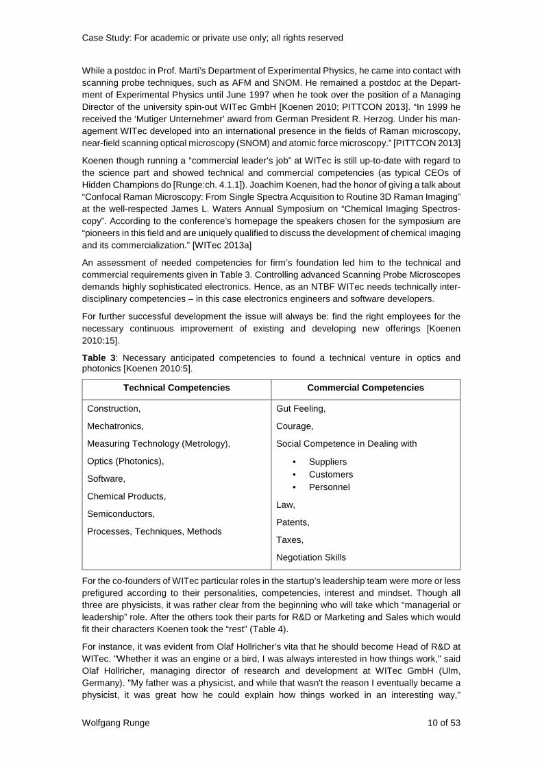
An assessment of needed competencies for firm’s foundation led him to the technical and commercial requirements given in Table 3. Controlling advanced Scanning Probe Microscopes demands highly sophisticated electronics. Hence, as an NTBF WITec needs technically inter-disciplinary competencies – in this case electronics engineers and software developers.
For further successful development the issue will always be: find the right employees for the necessary continuous improvement of existing and developing new offerings [Koenen 2010:15].
Table 3 : Necessary anticipated competencies to found a technical venture in optics and photonics [Koenen 2010:5].
Technical Competencies Commercial Competencies
Construction,
Mechatronics,
Measuring Technology (Metrology),
Optics (Photonics),
Software,
Chemical Products,
Semiconductors,
Processes, Techniques, Methods
Gut Feeling,
Courage,
Social Competence in Dealing with
• Suppliers • Customers • Personnel
Law,
Patents,
Taxes,
Negotiation Skills
For the co-founders of WITec particular roles in the startup’s leadership team were more or less prefigured according to their personalities, competencies, interest and mindset. Though all three are physicists, it was rather clear from the beginning who will take which “managerial or leadership” role. After the others took their parts for R&D or Marketing and Sales which would fit their characters Koenen took the “rest” (Table 4).
For instance, it was evident from Olaf Hollricher’s vita that he should become Head of R&D at WITec. "Whether it was an engine or a bird, I was always interested in how things work," said Olaf Hollricher, managing director of research and development at WITec GmbH (Ulm, Germany). "My father was a physicist, and while that wasn't the reason I eventually became a physicist, it was great how he could explain how things worked in an interesting way,"

Case Study: For academic or private use only; all rights reserved
Wolfgang Runge 11 of 53
remembered Hollricher. "All children are curious, but if you want to get a good answer about how things work, ask a physicist!" [Hollricher 2003]
A case of father-and-son affinity combined with a fascination for lasers led Hollricher to work with electron microscopy and superconductors at the Julich Research Center (Jülich, Ger-many), and near-field optics and microscopy at the University of Ulm (Germany) during a post doctorate under Prof. Othmar Marti at the Institute of Experimental Physics.
Under Marti's tutorship, Hollricher met a couple of like-minded fellows, Joachim Koenen and Klaus Weishaupt, each with his own expertise. After a few years developing near-field micro-scopes at the University of Ulm, the three men answered a commercial request from a US University for such a microscope, and started WITec (Wissenschaftliche Instrumente und Tech-nologie) GmbH [Hollricher 2003].
Klaus Weishaupt did his doctoral degree in 1996 at the Ulm University (“Brillouin spectroscopy of polymeric glasses under high pressure”) [Universität Ulm]. It seems that Klaus Weishaupt is a very application-oriented physicists, always looking to expand technology into new marketa-ble applications. This would bring him close to a marketing (and sales) role.
Foundation and development of the German WITec GmbH by three Ulm University physics postdocs ([Runge:Table I.41] and close-by text) represent a typical entrepreneurial case with Joachim Koenen as a driving member of the founder team focusing on learning-by-doing what is necessary for entrepreneurship (Table 4).
His basic conviction is that not only devices do go through development, also employees and leaders undergo development. Koenen went “from maid-of-all-work to leading the firm by goal setting and strategy or non-organic growth by acquiring other firms.” [Koenen 2010:37].
Joachim Koenen’s training on the job included the following areas [Koenen 2010:14]:
• Finance • Salary and Fringes • Labor • Contract Law • Patents • Customs, Import, Export • Organization • Procurement.
Examples of contemporary entrepreneurs may serve as role models which affect intention. For instance, J. Koenen emphasized the significance of an entrepreneurial example through strengthening self-confidence and self-motivation: “If he/she can do it, I can do it too.” Further-more, he had a self-employed father-in-law (personal communication and [Koenen 2010:4]).
There is a number of entrepreneurs owing much of their success to parental education or inher-ited or won family contacts. WITec GmbH could take advantage from two factors. One of the founders, J. Koenen, got a loan from his father-in-law who also served as a role model for being self-employed.
WITec’s founders seem to reflect the prototypes of entrepreneurs in scientific instruments. And there seems to be even notable differences in industry segments in attracting entrepreneurial personalities. Entrepreneurs may take big risks to bring the latest scientific tools to market. For instance, the people who take personal risks to bring new scientific instruments to market are a special breed. Many of these entrepreneurs are well-educated scientists who could make a fine living working as consultants or as employees in high-technology companies. Yet they risk their livelihoods and their own money for the chance to start up their own firms [Reisch 2011].

Case Study: For academic or private use only; all rights reserved
Wolfgang Runge 12 of 53
In the development of the firm J. Koenen and O. Hollricher emerged as the commercial and technical leaders of WITec.
Table 4: Founders’ roles in the entrepreneurial triple of WITec.
WITec GmbH All from the University of Ulm
Dr. K. Weishaupt Doctorate in experimental physics; Managing Director Sales & Marketing
Dr. O. Hollricher; Doctorate in experimental physics; Managing Director and Head of Research & Development
Dr. J. Koenen Doctorate in experimental physics; Managing Director (CEO), responsible for the “rest,” e.g., general management, strategy, administration, human resources, etc. a)
a) Personal communication and [Koenen 2010:36].
Business Idea, Opportunity, Foundation and Product Developments Before founding WITec Koenen (and the other WITec co-founders) already thought about to found an Internet firm, but gave up their intentions when a new opportunity emerged [Koenen 2010:13]. That means there were already social ties and agreements among the to-be founders of WITec.
Right from founding a physics-based venture the three founders were able to take advantage from the progressive miniaturization of many high technologies, such as microelectronics and nanotechnology. When they started WITec key scientific-technical business ideas centered around [Koenen 2010:7]:
• New feedback for shear-force for Fiber-SNOM • XYZ sample scanning • Parfocal detection optics • Pulsed Force Mode (PFM) supplementary electronics for AFM.
According to Klaus Weishaupt, the company had humble beginnings [Rose 2011] – at Koenen’s home. Dealing with finances was at his home, but phone and fax messages were re-directed to the university. On the other hand, assembly and manufacturing of instruments or devices were done at the university (mechanical and electronics workshops and institute of experi-mental physics) according to the “Young Innovators” program of the State of Baden-Württem-berg [Koenen 2010:14].
In April 1997, Dr. Joachim Koenen gave a talk about Pulsed Force Mode (PFM) in Urbana-Champaign (University of Illinois). He spoke about an operating mode for atomic force micro-scopes developed in Ulm in which the microscope tip quasi dabs the sample surface by con-trolled periodic pulses (“tapping”). A problem of the conventional atomic force microscopy so far was that the shear forces that occur during scanning may result in damage to sensitive samples’ surfaces. The first respond to this issue was the "tapping mode." [Universität Ulm 1997]
Americans of the audience were not content with explanations, but ordered the handmade pro-totype from Ulm for acquisition by purchase. Like the audience in the US, Koenen assumed that there will be soon numerous universities and manufacturers deciding to purchase the com-plement system in Germany [Universität Ulm 1997].
Case Study: For academic or private use only; all rights reserved
Wolfgang Runge 13 of 53
In Illinois it came true, what Koenen and his colleagues suspected for a long time and secretly hoped, that it would in fact be possible to exploit the sample-sparing additional equipment for atomic force microscopes including installation and training commer-cially.
In their opinion with the raising amount of technical applications in the field of nanotechnology an adequate growing demand for nanotechnology tools would be an opportunity for entrepre-neurs. This would depend on the quality and the acceptance of the resulting products for techni-cal or consumer applications.
The heaviest need was seen for tools which not only depict and analyze samples but also manipulate or characterize various properties on the nanoscale in order to link nanoscopic effects to macroscopic behavior [Universität Ulm 1997].
The US University wanted to necessarily buy the device Koenen presented, but a German university must not sell anything. Therefore the three physicists, in addressing and with the support of the University and Prof. Marti, were encouraged to found WITec [Grimminger 2012].
The purchase contract in his pocket, in Ulm Koenen assessed the chances of his anticipated company by a simulation program on the computer – with promising results [Universität Ulm 1997; Koenen 2010:11].
Formally their structured process of founding was almost like a blueprint for a textbook: Before Ulm's young entrepreneurs set up their firm as a GmbH (LLC), they went for advice on legal form to the Chamber of Industry and Commerce (in German IHK), concerning organization of public funding to the County’s District Office (Landratsamt) and, according to expert recommen-dation, had simulated different scenarios of potential business development on the computer [Universität Ulm 2000b].
In essence, apart from their scientific/technical competencies, WITec’s founders had a com-plete company exposé with information on the firm’s legal form, qualification of contractors, three-year planning, sales planning, personnel cost planning, capital requirements, and market-ing strategies [Universität Ulm 2000b; Koenen 2010:11].
In June 1997 Dr. Koenen and the two experimental physicists, Dr. Olaf Hollricher und Dr. Klaus Weishaupt, founded WITec GmbH which was registered in August 1997 [Universität Ulm 1997]. The founders of WITec planned to sell what they have studied and built in the laboratory, atomic force microscopes with special features including the associated know-how.
WITec addressed the second generation of SPMs (Figure 5), “founding of a new generation of probe microscope firms. The most successful of those second-generation firms – such as Asylum Research in Santa Barbara or WITec in Ulm – have a distinctly transatlantic style in their personnel, their customer base, and their collaborations with user innovators.” [Mody 2014] (Emphases added)
Just two months after the presentation in Illinois, since October 1997, Dr. Koenen participated in the Baden-Württemberg support program “Young Innovators” (“Junge Innovatoren”) 1, jointly issued by the Ministries of Economics and Science. He was employed on a part-time position (half of the common salary) at the university and thereby partially exempt from financial pres-sure. The program also meant using the university’s infrastructure for further R&D to stretch necessary initial investments for the firm in time [Universität Ulm 2000b; Universität Ulm 1997].
By the end of October for the distribution of its systems, the Trio from Ulm assured a dream partner: the Topometrix GmbH, the German subsidiary of Topometrix Corporation in Santa Clara (CA), one of the world's leading manufacturer of atomic force microscopes at that time [Universität Ulm 1997; Koenen 2010:13].

Case Study: For academic or private use only; all rights reserved
Wolfgang Runge 14 of 53
The fact that the spin-out soon won Beiersdorf AG as a customer, exported to England and BASF SE and Henkel KGaA expressed interest in their systems exceeded their own expecta-tions [Universität Ulm 2000b].
In this constellation the entrepreneurs entered a new emerging market niche, because rehearse gentle precision measurements at the nanometer scale, still regarded as an academic luxury by industry a few years ago, were considered around 1997 as indispensable when sensitive surfaces must be investigated precisely – by automotive and semiconductor manufacturers as well as in the chemical and pharmaceutical industries [Universität Ulm 2000b].
SNOM history and related issues/problems of the technology are outlined by Koenen [2010:16-18]. Overcoming them led to the development of the first product, the alpha300 SNOM [Koenen 2010:19].
WITec’s first products or developments included [Koenen 2010:3,4,6-8]:
• Scanning Near-Field Optical Microscope (SNOM) alpha300 S (First Product, First Generation [Koenen 2010:19,20])
• Atomic Force Microscope alpha300 A • Confocal Raman Imaging Microscope (CRM) alpha300 R [Koenen 2010:21-27], and
later line extensions of its products, such as alpha500 R, alpha700 R • Pulsed Force Mode (PFM) (Second Product – PFM [Koenen 2010:8]) • WITecProject Software for analysis and evaluation of measurements.
Further developments did not only refer to the instruments and combinations of their functions and mediation via appropriate software, but also the development of an efficient device for microscope control (alphaControl [Koenen 2010:31-34]) ending with a “System-on-a-program-mable-Chip” for the controller [Koenen 2010:35].
The optical near-field microscope "alpha300 S" allowed images with a resolution of less than 100 nm, which is in the billionth range. Concerning AFM the "alpha300 A" obtained high-resolution images of surface structures. Information about the chemical composition and spatial distribution of substances were provided by the confocal Raman microscope, "alpha300 R". The last one found later applications, among other things, in cosmetics and pharmaceutical research [Deutscher Gründerpreis 2007].
The introduction of the first SNOM featured easy to use cantilever SNOM sensors for reliable optical imaging beyond the diffraction limit. In addition, the Pulsed Force Mode accessory AFM module for imaging of local stiffness and adhesion along with topography was successfully introduced to the AFM community.
With the release of the first Confocal Raman Imaging system in 1999, WITec outperformed the existing Raman mapping techniques in terms of sensitivity, speed and lateral resolution, pio-neering Raman spectroscopy as a tool for true 3D chemical imaging [WITec 2014].
WITec continuously launched new, highly-innovative technologies. And also PFM was further developed to Digital Pulsed Force Mode (DPFM) in 2003 [Koenen 2010:28-30].
In 2003 WITec introduced the Mercury 100 AFM, a completely new Atomic Force Microscopy (AFM) system, designed specifically for materials research and nanotechnology. The integrated scientific-grade research microscope and the Digital Pulsed Force Mode, the new measure-ment mode for AFM, allows non-destructive imaging of various material properties along with the topography. A modular design for the first time guaranteed upgrade possibilities from AFM to Confocal / Raman microscopy as well as Scanning Near-Field Optical Microscopy (SNOM) [WITec 2003a].
According to Olaf Hollricher [Fischer 2003] “The Mercury 100 AFM is one of the most versatile AFM systems for material sciences.” “The combination of AFM with the Digital Pulsed Force
Case Study: For academic or private use only; all rights reserved
Wolfgang Runge 15 of 53
Mode and a scientific optical microscope allows the analysis of a variety of previously inaccessi-ble material properties and in a very short measurement time.” “The cost-efficient upgrade from AFM to other scanning probe microscopy techniques is to this day unique and increases the flexibility of the system enormously.” The Mercury 100 AFM supports all standard AFM modes.
By 2004 WITec had gained an international reputation: Comet dust of the NASA Stardust-Mission was analyzed with German high-tech microscopes. WITec supplied a system for analyzing particles collected from the comet Wild 2 by the NASA Stardust spacecraft. The microscope was delivered to the Geophysical Laboratory of the Carnegie Institution of Washington in Washington DC, specialized in the analysis of extraterrestrial material [Deutscher Gründerpreis 2007].
A new modular microscope generation, the alpha300 series, enabled various new features and automatic measurement procedures to be employed for the first time. The alpha300 series allows the combination of different microscopy techniques in one instrument [Fischer 2006]. (Emphases added)
• The digital signal processing reduces noise to extremely low levels and significantly enhances data and image quality.
• The integrated software for measurement control is the key to the unique features of the alpha300 series. It navigates the user through the measurement tasks while intui-tively providing a user interface that changes automatically depending on the method used.
• The new high-resolution microscope generation is ideally suited for applications in ma-terials sciences, life sciences, pharmaceuticals and nanotechnology where a compre-hensive understanding of the sample structure and composition is a necessity.
• "The new alpha300 series addresses three different markets at the same time. These are SPM, optical Confocal Microscopy and chemical Raman Microscopy, all offering increasing market potential and opportunities" said Dr. Joachim Koenen, "Most of the new features are available for the first time and are only possible with a full digital con-trol unit." For advanced scanning probe microscopy imaging tasks, the alpha300 series integrates TrueScanTM, a dynamic position error correction system of the closed loop scan stage for the highest accuracy in scan movement, a piezo-driven scan stage with capacitive feedback-control and dynamic position control.
• Additionally, the ability to perform high speed frequency scans, also leads to lower measurement times. Fully automated procedures, such as the high-speed cantilever approach, the adjustment of cantilever focus and position or the light intensity adjust-ment facilitate straightforward operation and ease-of-use.
In November 2007 WITec introduced the alpha500 and alpha700 series of instruments. And, for instance, in 2010 the patent pending TrueSurface Microscopy for profilometric measure-ments convinced the experts and was distinguished by well-respected prizes [WITec 2014].
In the field of near-field microscopy WITec became a world leader [Deutscher Gründerpreis 2007]. Koenen saw his company well positioned for the future: "In order to keep our lead in development, we will continue working hard on innovative technologies. Connecting to the University of Ulm helps us, we have first-class access to sought-after professionals." [Deutscher Gründerpreis 2007]
By 2007 WITec sold most of its instruments/equipment to universities and research institutes, such as the Caltech (California Institute of Technology) or the Max-Planck-Institutes, generating 60 percent of its sales to such customers. The remaining percentage of sales is generated from the research-intensive industry [Deutscher Gründerpreis 2007].
The major markets for WITec microscopes are Europe, USA and Japan. For this reason, mar-keting and sales have been focused on the global market right from the start of the firm. Today,
Case Study: For academic or private use only; all rights reserved
Wolfgang Runge 16 of 53
the company is present in all major markets either directly or through well-known sales and distribution partners. The US was one of WITec’s largest single market. Therefore, already in 2002 the company launched a subsidiary in Illinois.
According to the company’s management a contribution to the overall growth of the company was the further development of its international presence through increasing the sales network or the opening of additional subsidiaries abroad.
WITec’s confocal Raman microscope CRM200 addressed particularly the pharmaceutical busi-ness and thus was seen as a guarantor for further growth of the company.
"Our devices were so successful because we have consistently set up a modular prod-uct concept," said Koenen. The product line includes three combinable microscopes [Deutscher Gründerpreis 2007].
The modular design of WITec microscopes allows, for instance, the integration of Confocal Raman and Scanning Probe Microscopy in one system. And this innovation instigated a boom in combined Raman/SPM systems.
Confocal Microscopy + Raman spectroscopy = 3D Imaging with chemical sensitivity [Koenen 2010:23-26]
With the release of the first Confocal Raman Imaging system in 1999, WITec outperformed the existing Raman mapping techniques in terms of sensitivity, speed and lateral resolution, pio-neering Raman spectroscopy as a tool for true 3D chemical imaging.
The combination of instruments and their functionality into one system found its equivalent on the software level. For instance, in 2004 WITec introduced new software for its Confocal Raman Microscope CRM 200 [WITec 2004a].
The “ScanControl Spectroscopy Plus” software module was designed specifically for high-resolution Raman imaging needs. It combines measurement control functions with extensive evaluation and image processing capabilities. Various filter utilities and imaging tools allow high-end image processing or 3D views of the Raman images. All Raman spectra of the meas-urement are stored and a complete Raman spectrum can be matched to every desired pixel. The obtained spectra can be easily evaluated, displayed or exported for publication. Using single Raman lines for imaging, the software generates different images of different chemical proportions of the same sample spot [WITec 2004a].
"Analyzing the samples automatically significantly accelerates the measurement cycles in routine experiments, guaranteeing rapid problem solving and an efficient return on investment" said Dr. Weishaupt. (Emphasis added) "The combination of Confocal Raman Imaging and Atomic Force Microscopy in an automated system for large samples is unique worldwide. For the first time it is possible to not only chemically but also structurally characterize large samples automatically for the most comprehensive and rapid surface inspection on the sub-micron and nanometer scale." Imaging applications involving systematic procedures and routine operations as well as large sample analysis benefited from the new automated design of the alpha500 and alpha700 series.
In 2009 WITec launched an upgrade for WITecProject, the WITecProject Plus software pack-age for advanced data evaluation and chemometric image processing. It features various tools for multivariate data analysis in the fields of Confocal Raman Imaging and Scanning Probe Microscopy, such as cluster analysis and principal component analysis. Thus, hidden structures in the images can be visualized automatically, leading to quick and consistent interpretation of the data. This included a variety of advanced patent-pending analysis tools and algorithms to enable comprehensive and user-friendly computerized data evaluation and image generation. The speed with which the extensive calculations behind the various algorithms and procedures

Case Study: For academic or private use only; all rights reserved
Wolfgang Runge 17 of 53
can be executed was unprecedented and provided a new level of capability in analysis opera-tions [WITec 2009a; Koenen 2010:36].
Financing, Networking, and Organization
WITec was funded initially with private money, essentially “bootstrapping” via 3F [Runge:ch. 4.3.3.1] which is not a bad thing, Weishaupt said, because it creates pressure to make profits as soon as possible. “If the fridge is empty, the pressure is greater to make money than when you have millions from an investor to spend,” he said, adding that he does not want the com-pany to get listed on the stock exchange anytime soon. “We don’t want to sell. It’s better when the profits go into your own pocket.” [Von Bubnoff 2007]
Capital requirements for founding the new firm could be derived from a sophisticated Profit & Loss projection (P&L; in German G&V – Gewinn- und Veerlestrechnung) in terms of a spread-sheet given by Koenen [2010:11]. Initial financing of the new venture WITec [Koenen 2010:13] was by:
• Founders’ money, • Bank loan (by a German savings bank; Sparkasse) and private loan, • bank overdraft (in German Kontokorrentkredit, Überziehungskredit), • Prize from Startup Competition.
Having had already customers on foundation facilitated initial financing of WITec. Dr. Koenen as the Managing Director of WITec had auditioned with his plan and an external capital require-ment of DM250,000 (€125,000) at four banks, of which three were willing to finance the project. The banks would grant a loan even up to DM500,000 without having any collateral if the appli-cant has no debt [FES 1998]. Furthermore, according to Koenen, particularly the participation at the 1997 Founders' Competition “StartUp” provided a tailwind for initial financing [Deutscher Gründerpreis 2007].
The 3F-component of the founders included a loan of DM50,000 (€25,000) from Koenen’s father-in-law ([Koenen 2010:13] and personal communication) and additionally there were €5,000 from the German President award in the framework of the initiative "Courageous entrepreneurs the country needs" [Grimminger 2012].
In the “Firmenwissen” database one finds that the LLC (WITec GmbH) was set up based on equal equity contributions of the partners – each contributing €8,691.96 (total share capital €26,075.88).
For the first thirteen years of its existence WITec followed a path or organic growth. For further development profit was reinvested into its research and product development and sales.
Locations
WITec has its origins in the University of Ulm (Albert-Einstein-Allee; Institute for Experimental Physics). Then WITec moved into the industrial area of Ulm (address: Hörvelsinger Weg) and, when also the related facility was too tight, it moved into a new own building in Science Park II of Ulm (address: Lise-Meitner-Straße). According to WITec "for location issues the Urban Pro-ject Development Company was a great help." In Ulm now ca. 40 employees in the areas of research, development, management, production, sales and marketing operate. Offices are located in Singapore and Marysville (USA) [Grimminger 2012]:
Initially, Ulm University let the company rent lab space, said co-founder Klaus Weishaupt. “Ulm is a very good place for high-tech start-ups,” he explained [Von Bubnoff 2007]
Starting in 2008 and after a construction period of thirteen months, WITec GmbH moved into its new headquarters building in Ulm. The new building contains customized production facili-
Case Study: For academic or private use only; all rights reserved
Wolfgang Runge 18 of 53
ties, seminar rooms and office space to meet WITec's requirements for developing and produc-ing its products. Light filled spaces and open structures dominate the architectural design of the building to create a creative and interactive work environment on four floors and more than 1,900 m2 [WITec 2009b]. Similarly, also Attocube Systems focuses on office space in a beautiful setting and an attractive workplace for its employees [Runge 2014b].
To meet the increasing demand for high resolution microscopy solutions, the new building was a necessity in order to secure future growth potential. The driving force behind the successful development was the highly sensitive Confocal Raman Microscope system, which allows three dimensional imaging of chemical compounds of various materials. Atomic Force Microscopy for structural surface analysis on the nanometer scale and Scanning Near-field Optical Micros-copy, capable of optically resolving structures below the diffraction limit, completed the product portfolio [WITec 2009b].
According to Dr. Koenen [Firmenpresse 2009] “With this investment, we have deliberately chosen the Science Park II in Ulm, as the environment shaped by science and high technology provides ideal opportunities for development for us."
The own new building is a reflection of Dr. Koenen’s conviction in 2007 about WITec’s further development. He saw the company well positioned for the future: "In order to keep our lead in development, we will continue working hard on innovative technologies. Connecting to the University of Ulm helps us, we have first-class access to sought-after professionals." [Deutscher Gründerpreis 2007] However, Dr. Koenen confessed: "Nevertheless, when I look back on the last ten years, I am still a little surprised by the success." [Deutscher Gründerpreis 2007]
And WITec keeps still connections with its academic origins. ”Our research department is coop-erating with the university. We also assign diploma theses to the university of applied sciences," said Harald Fischer, Marketing Director at WITec, for whom the location in the Science Park II “gold is worth.” [Grimminger 2012].
Networking and Cooperative Projects
Early on WITec cooperated also with other universities. For instance, together with the Institute of Technical Physics of the Kassel University of Applied Sciences (Germany) WITec ran a project (Oct. 1, 1999 – Dec. 31, 2002) dealing with near-field characterizations of near-field probes [WITec 2003b].
During WITec’s early years resolution in SNOM was associated with many discussions. The maximum resolution in a near-field image is determined by aperture size, probe-sample dis-tance and the sample itself. But there are also effects due to nonlinear interaction between the electromagnetic (optical) waves and the surface that often make image interpretation very complicate and give rise to so-called topography induced artifacts (cf. also Kassing and Oesterschulze [2001]).
WITec does not only cooperate with the Ulm University, but there was also a successful re-search project funded by the German Ministry of Economics (BMWi). The aim of the project was to develop in cooperation with the Institute of Lasertechnology (ILM), Ulm, new photon-counting techniques to be incorporated into the WITec Raman Imaging systems for comprehen-sive optical sample inspection [WITec 2008]. ILM (Institut für Lasertechnologien in der Medizin und Meßtechnik an der Universität Ulm) is an An-Institute of Applied Research [Runge:Table I.21] associated with Ulm University having ca. 50 employees. 2
At the ILM Angelika Rück (Group Leader for Microscopy) together with Thomas Wirth, Director of the Institute for Physiological Chemistry at Ulm University, set up the “Imaging Center” as a “Core Facility” (investment: ca. €1 million). Particularly, ILM and the University each got a new laser scanning microscope which are provided with a femto-second laser of the latest genera-tion. These instruments make it possible to carry out the so-called two-photon microscopy. The

Case Study: For academic or private use only; all rights reserved
Wolfgang Runge 19 of 53
focus was LifeCellImaging. Rück of ILM found that Confocal Raman Microscopy in combination with cluster analysis for data evaluation offered by WITec can be used for cell diagnostic (but not in the hospital) [BioPro 2010].
To study living cells in their physiological surroundings without damaging them is a highly sought after capability in life science. For instance, WITec’s alpha300 combines such a non-destructive method with the capability to identify chemical components inside a cell.
The significance of the ILM/WITec project was that the transfer of measurement technology was integrated with application from the beginning. Angelika Rück wanted to explore with various optical methods the growth of normal and neoplastic cells, which is tumors. If it were possible to distinguish the stages of growth of a tumor, that would be an important diagnostic tool for cancer therapy [Schäfer 2009].
So far, biologists and physicians investigated cells usually under the fluorescence microscope. They add a “marker” to the sample that attaches itself to certain cell components, and then watch the flashing of this substance. But that affects dramatically the metabolism of the cell, change it and in the end leads to death of the cell. Therefore the project was set up (with WITec) to watch cell growth (“cell differentiation”) without marker based on Confocal Raman Micros-copy.
Originally looking for noradrenaline the researchers found instead another hit: "With the cyto-chrome c we could identify the molecule that plays an important role in the respiratory chain" which is present in every cell and serves electron transfer. "Via cytochrome c, we learn about how the cell power facilities work and whether the cell will die soon," said the chemist. The researchers in Ulm thus had found a specific candidate, whose activity and distribution in the cell they can check during cell differentiation [Schäfer 2009].
Furthermore, WITec participated continuously in publicly financed projects (usually joint pro-jects – Verbundprojekte) as a means of contributions to revenue, source of financing own R&D, establishing connections with other firms and opening paths to potential future customers.
Relatedly, WITec is member of the (German) regional Competence Network [Runge:Figure I.39] ”PhotonicsBW.” PhotonicsBW is one of the nine regional competence networks of the trans-regional OptecNet Deutschland e.V. which is supported by the German Federal Ministry of Education and Research (BMBF) [PhotonicsBW 2010].
In 2008 WITec was appointed as one of the industry members of the Tumor Diagnostics Project ("Exprimage"), funded by the German Ministry of Research and Education (BMBF) in the con-text of biophotonics projects. The aim of the project was to employ highly innovative optical and biomolecular technologies to establish new capabilities in tumor diagnostics for physicians. WITec contributed its Raman imaging expertise [WITec 2008, BMBF 2007].
The €9.0 million joint project Exprimage (Aug. 1, 2007 – Sep. 30, 2010) was supported by the BMBF with €5.8 million. Partners were [BMBF 2007]:
• Carl Zeiss MicroImaging GmbH (Coordination) • Universitätsklinikum (University Hospital) Hamburg-Eppendorf • QIAGEN GmbH • RWTH (Technical University) Aachen • Universität Jena, Institut für Physikalische Chemie • WITec GmbH.
By 2009/2010 areas of application for WITec's Confocal Raman Imaging systems included polymer sciences, pharmaceuticals, life science, geoscience, thin films and coating analysis, semiconductors, and nanotechnology.
Case Study: For academic or private use only; all rights reserved
Wolfgang Runge 20 of 53
For the life science area it was already demonstrated that confocal Raman imaging provides the ability to non-invasively reflect the chemical properties of emulsions three dimensionally with the highest resolution.
Organization
As operational units WITec’s location in Ulm (Germany) has typically research, development, manufacturing, marketing and sales and administration (departments) [Grimminger 2012]. The external resource management of WITec’s cooperative and networking partners as part of its organization has been described above.
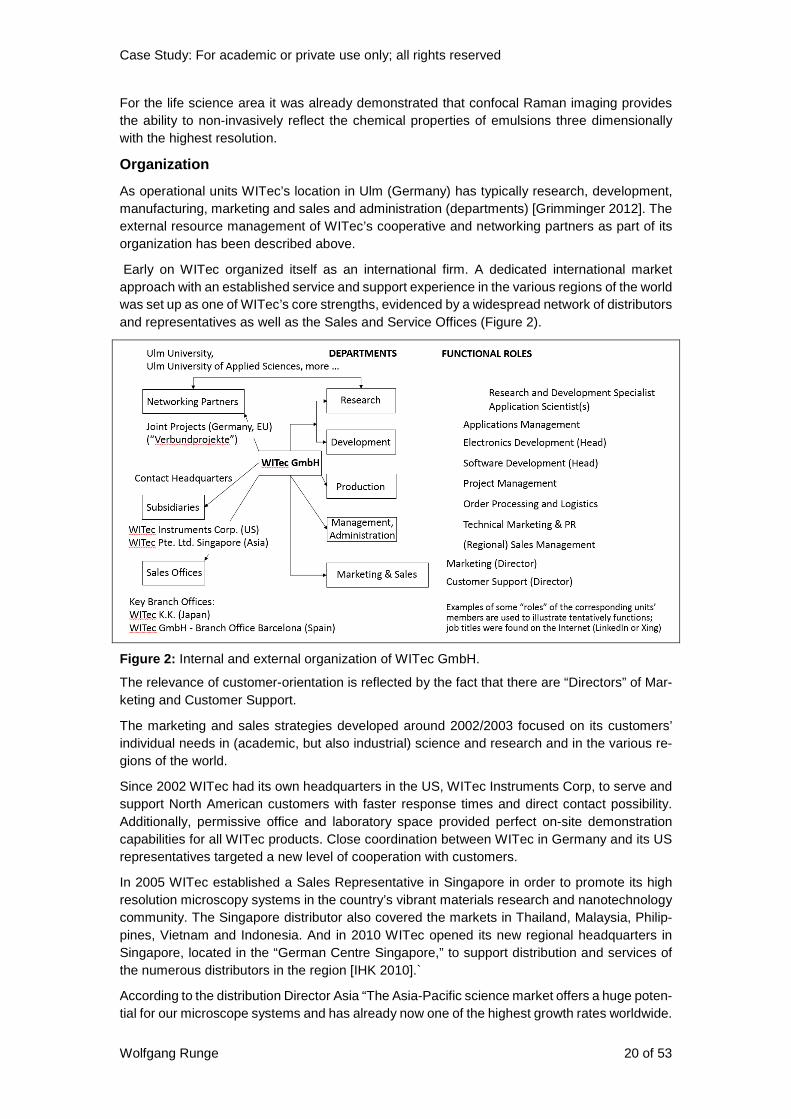
Early on WITec organized itself as an international firm. A dedicated international market approach with an established service and support experience in the various regions of the world was set up as one of WITec’s core strengths, evidenced by a widespread network of distributors and representatives as well as the Sales and Service Offices (Figure 2).
Figure 2: Internal and external organization of WITec GmbH.
The relevance of customer-orientation is reflected by the fact that there are “Directors” of Mar-keting and Customer Support.
The marketing and sales strategies developed around 2002/2003 focused on its customers’ individual needs in (academic, but also industrial) science and research and in the various re-gions of the world.
Since 2002 WITec had its own headquarters in the US, WITec Instruments Corp, to serve and support North American customers with faster response times and direct contact possibility. Additionally, permissive office and laboratory space provided perfect on-site demonstration capabilities for all WITec products. Close coordination between WITec in Germany and its US representatives targeted a new level of cooperation with customers.
In 2005 WITec established a Sales Representative in Singapore in order to promote its high resolution microscopy systems in the country’s vibrant materials research and nanotechnology community. The Singapore distributor also covered the markets in Thailand, Malaysia, Philip-pines, Vietnam and Indonesia. And in 2010 WITec opened its new regional headquarters in Singapore, located in the “German Centre Singapore,” to support distribution and services of the numerous distributors in the region [IHK 2010].`
According to the distribution Director Asia “The Asia-Pacific science market offers a huge poten-tial for our microscope systems and has already now one of the highest growth rates worldwide.
Case Study: For academic or private use only; all rights reserved
Wolfgang Runge 21 of 53
Therefore, the timing for the establishment of a subsidiary is perfect." The rationale for selecting Singapore is: “As a regional hub for the Asia-Pacific region, Singapore is the perfect choice for an office in this region.” [IHK 2010].
In 2012 WITec further expanded its worldwide presence with the opening of regional offices in Japan and Spain (WITec K.K., Kawasaki-shi Kanagawa, Japan and WITec GmbH – Branch Office Barcelona, Spain).
Overall there are three WITec Contact Headquarters by global regions:
• Germany (and Europe): WITec GmbH (in Ulm), where all WITec products are devel-oped and produced
• North America: WITec Instruments Corp. Knoxville, Tennessee • Asia: WITec Pte. Ltd.Singapore (International Business Park, German Centre).
The landscape of worldwide representations of WITec are displayed by Koenen [2010:12]:
• BRICS States: Brazil, Russia, India, China, South Africa • Special in Europe: France, Hungary, Italy, Netherlands, Poland, Romania, Spain
(WITec GmbH – Branch Office Barcelona), UK • Middle East: Israel, United Arab Emirates • Special in Asia: Indonesia, Japan (WITec K.K.), South Korea, Taiwan, • Special in North America: Canada, • South and Middle America: Chile, Mexico, • New Zealand (also for Australia).
To strengthen its US business in 2009 WITec hired a new managing director for its US sub-sidiary bringing in Robert Hirche, a “business veteran.” He will coordinate the established network of regional sales representatives across the US and support the growing installed base of Raman, NSOM and AFM solutions. Hirche has a wealth of experience in sales, marketing and distribution of scientific instrumentation in the fields of surface characterization, nanotech-nology and microscopy – with more than 25 years of experience in this market segment.
There are large coordination effort needs for WITec’s management to keep consistently high-quality services to customers and provide demonstrations of WITec’s products and contribute to WITec’s growth strategy. For this reason there are International WITec Distributor Meetings in Ulm.
For instance, in early February 2012 more than 30 representatives of international WITec dis-tributors met in Ulm, Germany. “The meeting’s theme was “The Seed Crystal for Future Growth” reflecting the spirit of the company aiming to achieve the next significant growth level and to further strengthen WITec’s position as a market leader in the field of high-resolution microcopy. Main topics of the meeting included the ongoing and future activities in the technical as well as marketing fields in order to intensify the consulting strength of the WITec sales force.” [WITec 2012a]
After the economic and financial crisis in 2009 Russia suffered from a heavy recession. But by 2010 Russia became one of the fastest growing economies. Furthermore, in the context of a general program to modernize the economy, with Germany as the most important partner for high-tech, the Russian Government supported broadly R&D of their firms with loans.
In particular, already in 1998 a government program for nanotechnology was initiated to build related industries with a turnover of approximately €30 billion. The state-owned enterprise ROSNANO provided favorable loans with a volume of more than €3 billion, creating important impetus for a variety of projects. Accordingly in the region around Novosibirsk one of four spe-cial economic zones for technical innovation with a focus on nanomaterials and nanotechno-logies was created [PresseEcho 2010].
Case Study: For academic or private use only; all rights reserved
Wolfgang Runge 22 of 53
In this climate a future Russian competitor of WITec, NT-MDT, emerged strongly (see below Competition, Table 7).
Due to the favorable conditions, WITec saw a good opportunity for further expansion. According to its Sales Manager Europe Dr. Toporski “We are working with a partner in Russia, but we were not really active yet in Russia. The threshold was too high with respect to the country that is so different from ‘the West’.” [PresseEcho 2010]
This attitude changed fundamentally with the contact to the CEO of “Russland Experten Con-sulting,” Nathalie Wenzel. “We had finally someone at our side, who perfectly masters not only the language and interprets the business practices correctly, but above all has excellent, essential contacts with decision makers from policy, science and industry," said Dr. Toporski. Hence, WITec could successfully start promotion by various means [PresseEcho 2010].
"The reasons for the success of our product line were the implementation of new developments and the consequent accomplishment of the modular product philosophy" said Dr. Koenen. "The current boom of nanoscale research significantly contributes to our ongoing positive sales growth," added Dr. Weishaupt [WITec 2007].
Continuous improvements and diversification will strengthen WITec's leading position in the market. "To secure our leading edge we will work constantly on innovative technologies and will continuously launch new products," said Dr. Hollricher [WITec 2007].
Remarks Concerning Corporate Culture
WITec has a strong and stable leadership team with technical and commercial expertise and attitude and very loyal employees, in particular in the research and development areas. There seems to be a high degree of identification of owners and employees at all levels with the company.
Employee loyalty is also associated with deep knowledge of technology and also continuous learning activities.
In particular, there is a very stable situation in R&D, electronics and software personnel. A number of people were also from the Ulm University institute WITec was spun out of. This can be seen from the inventors‘ names of the patents and when these patents were applied for (Table 6), the names of presenters of “alphaControl” at a meeting of the American Physical Society (November 2005) [Spizig et al. 2005] and comparing this with WITec‘s TrueSurface Microscopy Development Team from 2010/2011 [R&D Magazine 2011].
• Olaf Hollricher, Principal Developer • Wolfram Ibach • Detlef Sanchen • Peter Spizig • Gerhard Volswinkler.
The development of the TrueSurface microscope demonstrates executing interdisciplinary team and project work as well as customer and quality orientation.
Representatives of the TrueSurface project team included [R&D Magazine 2011]:
Case Study: For academic or private use only; all rights reserved
Wolfgang Runge 23 of 53
• Harald Fischer (Director Marketing) • Robert Hirche (Managing Director of the US WITec branch office) • Olaf Hollricher (Managing Director R&D) • Wolfram Ibach (Head of Software Development) • Detlef Sanchen (Senior Software Engineer) • Peter Spizig (process control; author of “Scanning Probe Microscope Control:” in
Imaging & Microscopy 9, 52-55, 2007) • Gerhard Volswinkler (Electronics) • Jianyong Yang (Applications Scientist in the US).
Innovation Persistence, Expansion and Diversificati on With twelve years of existence WITec leaves the class of new technology-based firms (NTBFs; [Runge:ch. 1.1.1.2]) and WITec can be assumed to develop largely similar to a German Hidden Champion [Runge:ch. 4.4.1].
Developments of WITec during the period 2010-2013 are characterized by product extensions and related software, but there are also new approaches concerning modes of growth and product types.
Customer-orientation and a dedicated international market approach in the various regions of the world are two of WITec’s key strengths, evidenced by its widespread network of distributors and representatives and subsidiaries. In 2012 WITec expanded its worldwide presence with the opening of regional offices in Japan and Spain [WITec 2014].
WITec’s core competence, a modular product line open to combination of different microscopy techniques in one instrument, remained at the center of offerings and related activities and represents.
For the first dozen years of its existence WITec developed along innovation and investment persistence and organic growth. But, rather than following only organic growth via own profit and cash flow in 2010 WITec turned also to non-organic growth [Runge:Figure I.127] to achieve its goals as a part of its expansion strategy.
With the acquisition of a majority ownership of omt optische messtechnik GmbH based also in Ulm (founded in 1999 with nine employees in 2010) WITec broadened its technology and product portfolio of leading high-resolution microscope systems for structural, optical and chem-ical analysis to more innovative optical measurement solutions. According to Elektronischer Bundesanzeiger [EB] (Electronic Federal Announcements for WITec 2011) WITec’s share in omt was 51 percent.
"Our goal is to expand our market leadership in the field of 3D surface analysis. omt opens up very efficiently more strategic areas that will bring us additional growth, "explained Dr. Koenen. "In the future we may serve new customer groups, particularly in the fully automated process control for industrial applications." [Bio-Pro 2010b]
Specifically WITec’s goal was to enhance its market position in the field of measurement technology for industrial applications supplementing WITec’s product range and offering new perspectives for joint marketing activities. omt provides optical metrology tools and is particu-larly strong in industrial process control of parameters such as film thickness, color, sheet resistance, moisture and chemical composition. For these types of measurements omt provides in-line and laboratory devices leveraging techniques such as reflectometry, spectral ellipsome-try, video microscopy and spectroscopy. omt was established to continue to operate as an independent company in the future [WITec 2010; BioPro 2010b].

Case Study: For academic or private use only; all rights reserved
Wolfgang Runge 24 of 53
Furthermore, omt has specialized in the development and production of customized, automated optical measurement systems for the analysis of thin layers in laboratory and industry. The optical (non-contact) measurement systems are used, for example, in the glass, photovoltaic, paper and automotive industries and in research laboratories [WITec 2010a; BioPro 2010b].
In line with its growth strategy WITec continuously launches new, highly-innovative technolo-gies. Correspondingly, in 2010 the patent pending TrueSurface Microscopy emerged strongly [WITec 2010a], convinced the experts and was distinguished by well-respected prizes [WITec 2014].
WITec’s True Surface Microscopy has been selected as a winner of the prestigious 2011 R&D 100 Award. It honors the WITec innovation as one of the 100 most technologically significant developments of the year. This is the second time that WITec won the R&D 100 Award, the first was won in 2008. Previously in March 2011, TrueSurface Microscopy received the PITTCON 2011 Editors Gold Award [WITec 2011a; WITec 2011b].
The new TrueSurface Microscopy option was a response to the issue of confocal Raman imag-ing that samples may require extensive preparation in order to obtain a certain surface flatness. It allows confocal Raman imaging guided by surface topography. The topographic coordinates measured from an integrated profilometer are used to perfectly follow the sample surface in confocal Raman imaging mode. The result is an image revealing optical or chemical properties at the surface of the sample [WITec 2011a].
The integrated sensor for optical profilometry is the core element of this imaging mode. Large-area topographic coordinates from the profilometer measurement can be precisely correlated with the large-area confocal Raman imaging data. This allowed for the first time confocal Raman imaging along heavily inclined, sloping or very rough samples with the true surface held in constant focus while maintaining the highest confocality. With the new imaging mode sam-ples can now be effortlessly and automatically characterized as they are. Complete system control as well as extensive data evaluation are integrated within the WITec Control and WITec Project software environment characterization [WITec 2010b].
“Roughness of surfaces” is an important measure in the context of quality control via SPM techniques.
In 2011 WITec presented results acquired with a time-correlated single photon counting mod-ule. A blue light-emitting diode was characterized by means of spatially and temporally resolved electro- and photoluminescence measurements which are standard tools for the characteriza-tion of optoelectronic devices. The study included micro-electroluminescence and time-resolved emission spectroscopy measurements as well as imaging of the signal propagation through the device [WITec 2011b].
Notably Dr. Hollricher has dealt with optoelectronics and has a patent when he worked at the Julich Research Center (Jülich, Germany): Optoelectronic diode and component containing same (US5859464 (A) from 1999-01-12, priority 1994-03-29).
In 2013 WITec launched StrobeLock, a time-correlated single photon counting (TCSPC) meas-urement option. The imaging modes include Fluorescence Lifetime Imaging Microscopy (FLIM) and Time-Resolved Luminescence Microscopy (TRLM), which can be integrated with the WITec alpha300 and alpha500 microscope series. StrobeLock is comprised of a pulsed excita-tion laser system combined with a TCSPC detector [WITec 2013b; Imaging & Microscopy 2013].
StrobeLock facilitates the acquisition of additional material contrasts hidden in the time function of a fluorescence or luminescence signal and allows them to be perfectly linked with Raman, SNOM or AFM imaging. It enables a variety of measurement possibilities for an improved and
Case Study: For academic or private use only; all rights reserved
Wolfgang Runge 25 of 53
more comprehensive understanding of a sample's properties and is specifically suited for ma-terials science.
The possibility to switch between time-resolved and conventional mode enables the microscope user to conveniently choose the preferred measurement technique. “StrobeLock complements the modular WITec microscope systems with customized solutions for the most accurate Flu-orescence Lifetime Imaging and Time-Resolved Luminescence Microscopy,” said Dr. Koenen, “This exceptional development significantly extends the capabilities of the WITec microscope series and opens a new field of application for a more comprehensive sample characterization.” [WITec 2013b; Imaging & Microscopy 2013].
Again it was the modular design of the WITec microscope series and the attachment of a time correlated single photon counting module to the alpha300 or alpha500 confocal microscope series which makes possible several types of spatial and time-resolved measurements, for instance also electro- and photoluminescence decay imaging.
As also Angelika Rück at the ILM institute (Ulm) deals with FLIM [BioPro 2010a] one can hy-pothesize that via a previous cooperation of WITec with ILM related contacts and communica-tions provided some impetus or input, respectively, for the development of StrobeLock.
At present, optical microscopes represents a major share in the microscopy market. However, it was assumed to lose its stake to scanning probe and electron microscopes in the near future [Chai 2011]
According to TechNavio, as the pace of the development of high-tech is tremedous, there is a much greater demand for advanced error detection solutions (“Failure Analysis Equipment”). In recent years, more and more industries have regarded electron microscopes as an efficient means of fulfilling this need. The market's value and growth is divided essentially between three lines of products and Scanning Electron Microscopes (SEMs) are responsible for close to half of all market revenue. TechNavio analysts predict that the Global Electron Microscope Market will climb at a CAGR of 9.9 percent over the 2012-2016 period [TechNavio].
Enlargement and growth of the SEM market by expanding the scope of SEMs from R&D to production and quality control had already been noted in 2006 by JETRO [2006].
In 2012 there emerged an opportunity of combining WITec’s Raman core strengths with a mi-croscopy technology it did not deal with so far, electron microscopy. Note that Dr. Hollricher worked already with electron microscopy at the Julich Research Center.
Since early 2012 specialists from Germany, the Czech Republic, and Switzerland were jointly advancing novel, correlative microscope techniques to provide new opportunities for the de-tailed analysis of nanostructures as part of the EU-funded project UnivSEM, which supports the development of supplementary analysis tools for scanning electron microscopes (SEM). UnivSEM received funding from the European Union Seventh Framework Program (FP7/2007-2013) under grant agreement No. 280566. 3 The funding period is from April 2012 to May 2015. [WITec 2014a; NanUUU 2014].
As part of the UnivSEM project, TESCAN ORSAY HOLDING, a multinational leading company in ion and electron microscopy and WITec successfully introduced a correlative microscopy technique which combines scanning electron microscopy (SEM) with Raman microscopy.
The resulting RISE (Raman Imaging and Scanning Electron) Microscopy technique enables for the first time ultra-structural and chemical imaging with one microscope. Both WITec and TESCAN jointly launched the RISE Microscopy at Analytica 2014.
TESCAN and WITec arranged worldwide sales and after-sales cooperation for the RISE Micro-scope to take advantage of the synergy effects of both companies.
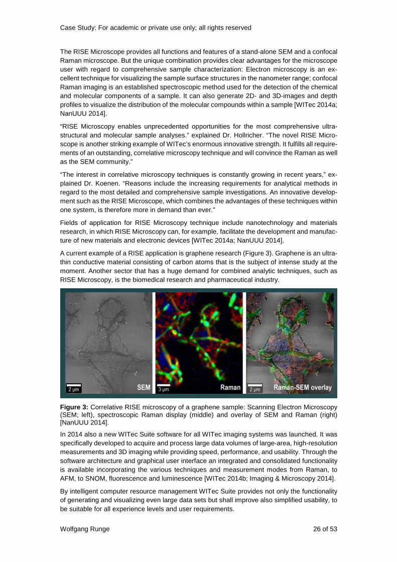
Case Study: For academic or private use only; all rights reserved
Wolfgang Runge 26 of 53
The RISE Microscope provides all functions and features of a stand-alone SEM and a confocal Raman microscope. But the unique combination provides clear advantages for the microscope user with regard to comprehensive sample characterization: Electron microscopy is an ex-cellent technique for visualizing the sample surface structures in the nanometer range; confocal Raman imaging is an established spectroscopic method used for the detection of the chemical and molecular components of a sample. It can also generate 2D- and 3D-images and depth profiles to visualize the distribution of the molecular compounds within a sample [WITec 2014a; NanUUU 2014].
“RISE Microscopy enables unprecedented opportunities for the most comprehensive ultra-structural and molecular sample analyses.” explained Dr. Hollricher. “The novel RISE Micro-scope is another striking example of WITec’s enormous innovative strength. It fulfills all require-ments of an outstanding, correlative microscopy technique and will convince the Raman as well as the SEM community.”
“The interest in correlative microscopy techniques is constantly growing in recent years,” ex-plained Dr. Koenen. “Reasons include the increasing requirements for analytical methods in regard to the most detailed and comprehensive sample investigations. An innovative develop-ment such as the RISE Microscope, which combines the advantages of these techniques within one system, is therefore more in demand than ever.”
Fields of application for RISE Microscopy technique include nanotechnology and materials research, in which RISE Microscopy can, for example, facilitate the development and manufac-ture of new materials and electronic devices [WITec 2014a; NanUUU 2014].
A current example of a RISE application is graphene research (Figure 3). Graphene is an ultra-thin conductive material consisting of carbon atoms that is the subject of intense study at the moment. Another sector that has a huge demand for combined analytic techniques, such as RISE Microscopy, is the biomedical research and pharmaceutical industry.
Figure 3: Correlative RISE microscopy of a graphene sample: Scanning Electron Microscopy (SEM; left), spectroscopic Raman display (middle) and overlay of SEM and Raman (right) [NanUUU 2014].
In 2014 also a new WITec Suite software for all WITec imaging systems was launched. It was specifically developed to acquire and process large data volumes of large-area, high-resolution measurements and 3D imaging while providing speed, performance, and usability. Through the software architecture and graphical user interface an integrated and consolidated functionality is available incorporating the various techniques and measurement modes from Raman, to AFM, to SNOM, fluorescence and luminescence [WITec 2014b; Imaging & Microscopy 2014].
By intelligent computer resource management WITec Suite provides not only the functionality of generating and visualizing even large data sets but shall improve also simplified usability, to be suitable for all experience levels and user requirements.
Case Study: For academic or private use only; all rights reserved
Wolfgang Runge 27 of 53
“WITec imaging systems are well-known for their exceptional imaging qualities. Unprecedented performance and speed facilitate the acquisition of large data volumes and the generation of 3D images and large-area scans.” explained Dr. Hollricher, “The capabilities of WITec Suite match perfectly with the requirements for high-speed data acquisition and processing of large data volumes and provide an accomplished combination of comprehensive data analysis and ease-of-use.” [WITec 2014b; Imaging & Microscopy 2014]
WITec Suite includes (Figure 4) Control FOUR, a software tool for measurement control and data acquisition, and Project FOUR, a data evaluation and processing software. The license terms facilitate the installation of Project FOUR on an unlimited number of computers permitting the user to process data and generate images wherever required.
Key Metrics Key metrics of growth of new technology-based firms (NTBFs) is based on developments of revenues and number of employees as the related indicators [Runge:638-640]. For recent years the company claimed to generate on average growth rates of ten percent a year [Bio-Pro 2010] and WITec was always profitable, right from the outset [WITec 2007].
An idea about the level of WITec’s profitability can be obtained from [EB] (Elektronischer Bundesanzeiger – Electronic Federal Announcements for WITec 2011): Related to revenue of €11.17 million “Profit after Tax” in 2011 was €629,000 (which is 5.63 percent of revenue). From the same source expenses for R&D in 2011 were €620,000. With an R&D intensity of 5.55 percent WITec belongs, as expected, to the class of top-value technology ventures (TVT, [Runge:Table I.1].). The number of employees in R&D were 8.
In 2011 there was a productivity (revenue per employee) of €321,000 per employee [EB].
The price of WITec’s instruments is upwards €120,000 [Grimminger 2012]. The typical range of prices for these high-tech instruments can be found in the JPK Instruments case [Runge 2014a].
The gross margin from WITec’s instruments is estimated to be typically about 30 percent. The gross margin of a company is total sales revenue minus its cost of goods sold, divided by the total sales revenue, expressed as a percentage.
Concerning customer structure ca. 60 percent are from academia and 40 percent from industry [Deutscher Gründerpreis 2007]. This distribution with a majority of public universities or re-search institutes as customers means that revenue may be notably sensitive towards federal and state budgets, spending and fiscal restrictions or consolidations.
WITec’s export rate is ca. 75 percent [EB] (Elektronischer Bundesanzeiger – Electronic Federal Announcements for WITec 2012). As WITec is focused to a large extent on customers in North America and Asia notable variations of currency exchange rates will affect its revenues.
The timelines of WITec’s revenues and numbers of employees are given in Table 5. For the employees’ numbers after 2002, when the US subsidiary was set up, it is mostly not clear whether the numbers refer to total number of employees in Ulm and abroad or whether they refer only to the Ulm location.
The significant dip in 2012 revenue was attributed by WITec to planned spending cuts in the public sector in the US due to the so-called sequester to come into force in 2013 and also Mediterranean European states still suffering from economic problems, inducing difficult to estimate consequences for the expenditure in the scientific field. 4 Although many US customers had approved projects of public funding bodies, the funds were not released or only very late.
In 2011 omt had serious slumps in demand for its photovoltaic business and generated heavy losses [EB]. Later the omt Optische Messtechnik GmbH filed for bankruptcy [EB] (Report 2012).

Case Study: For academic or private use only; all rights reserved
Wolfgang Runge 28 of 53
Table 5: Revenues and numbers of employees of WITec GmbH.
Year Revenue (€, mio.) No. of Employees References, Remarks
1997 0.051 3 [Koenen 2010:11]
1998 0.54 Estimated from Koenen 2010:11] c)
1999 1.55 Estimated from [Koenen 2010:11] c)
2000 2.15; 3 11 [Universität Ulm 2000a; Emes 2005]
2001 2.21 Estimated from [Koenen 2010:11] c)
2002 3.29 Estimated from [Koenen 2010:11] c)
2003 – –
2004 5.50 24 Previous WITec Website
2005 {6.05) a)
2006 {6.66} a) 24 b)
2007 7.1 {7.32} a) 27 b) [Deutscher Gründerpreis 2007]
2008 {8.05} a)
2009 8.50 {8.86} a) 30 30 employees in Ulm, 4 in US, 2 in Asia [Koenen 2010:2]
2010 9.80 b) {9.74} a) 33 31 [EB]
2011 11.17 b) {10.72} a) 40, 37 b) [Grimminger 2012]; total vs. Ulm?
2012 9.75 b) 39
2013 10.64 d) 50 [NanUUU 2014]; 42 in Ulm, 8 abroad?
a) Values in braces are calculated from average growth rates of WITec of 10% [BioPro 2010], the series starts with 2004 data and then data for 2007 and 2009-2011 represent checks of appropriateness; b) Elektronischer Bundesanzeiger (Electronic Federal Announcements) [EB]; c) Verbal comment: revenue projections were almost be met; d) from the Firmenwissen database (12/8/2014).
Intellectual Properties Apart from various trademarks like PFM, FAST RAMAN IMAGING or WITec as a word mark the company had 19 patents or patent applications in 6 patent families in early 2010 [Koenen 2010:9]. By 2012 36 patents or applications in 10 families containing German (DE) patents or patent applications, respectively show up in the DEPATISnet database (of the German Patent and Trademark Office, DPMA) (Table 6).
Additional information was extracted from the databases of the European Patent Office (EPO) and the US Patent and Trademark Office (US PTO).
Early on many of WITec’s developments and products were protected as intellectual properties (patents) [Koenen 2010:9]. The essential protection purposes of the patents had defensive characters or serve as a basis for commercial transactions (such as licensing or patent swaps).
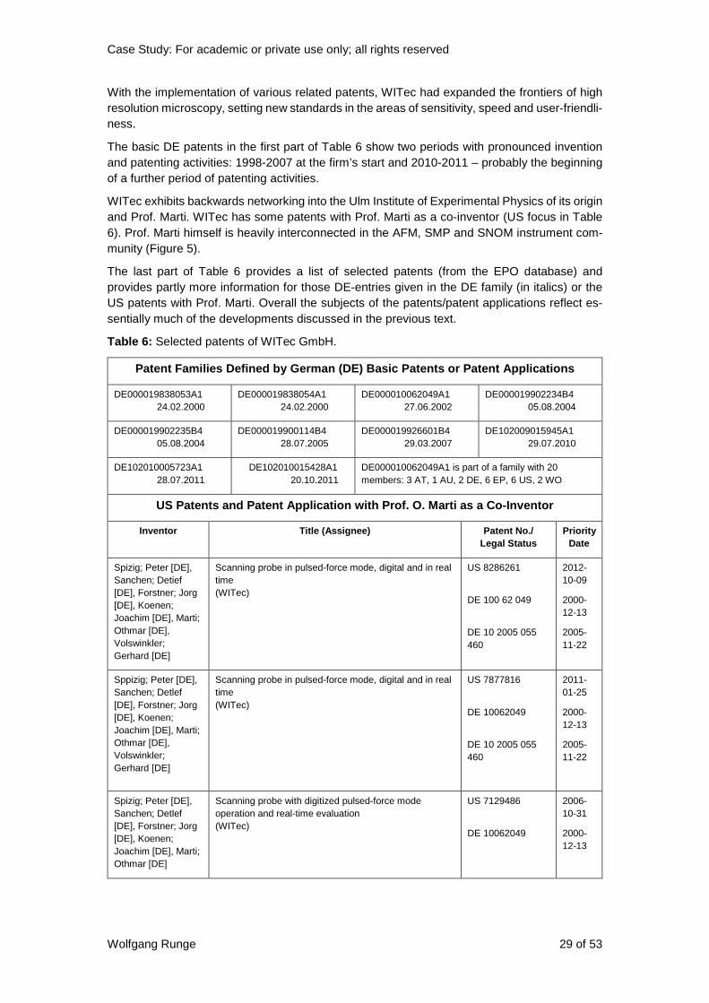
Case Study: For academic or private use only; all rights reserved
Wolfgang Runge 29 of 53
With the implementation of various related patents, WITec had expanded the frontiers of high resolution microscopy, setting new standards in the areas of sensitivity, speed and user-friendli-ness.
The basic DE patents in the first part of Table 6 show two periods with pronounced invention and patenting activities: 1998-2007 at the firm’s start and 2010-2011 – probably the beginning of a further period of patenting activities.
WITec exhibits backwards networking into the Ulm Institute of Experimental Physics of its origin and Prof. Marti. WITec has some patents with Prof. Marti as a co-inventor (US focus in Table 6). Prof. Marti himself is heavily interconnected in the AFM, SMP and SNOM instrument com-munity (Figure 5).
The last part of Table 6 provides a list of selected patents (from the EPO database) and provides partly more information for those DE-entries given in the DE family (in italics) or the US patents with Prof. Marti. Overall the subjects of the patents/patent applications reflect es-sentially much of the developments discussed in the previous text.
Table 6: Selected patents of WITec GmbH.
Patent Families Defined by German (DE) Basic Patent s or Patent Applications
DE000019838053A1 24.02.2000
DE000019838054A1 24.02.2000
DE000010062049A1 27.06.2002
DE000019902234B4 05.08.2004
DE000019902235B4 05.08.2004
DE000019900114B4 28.07.2005
DE000019926601B4 29.03.2007
DE102009015945A1 29.07.2010
DE102010005723A1 28.07.2011
DE102010015428A1 20.10.2011
DE000010062049A1 is part of a family with 20 members: 3 AT, 1 AU, 2 DE, 6 EP, 6 US, 2 WO
US Patents and Patent Application with Prof. O. Mar ti as a Co-Inventor
Inventor Title (Assignee) Patent No./ Legal Status
Priority Date
Spizig; Peter [DE], Sanchen; Detief [DE], Forstner; Jorg [DE], Koenen; Joachim [DE], Marti; Othmar [DE], Volswinkler; Gerhard [DE]
Scanning probe in pulsed-force mode, digital and in real time (WITec)
US 8286261
DE 100 62 049
DE 10 2005 055 460
2012-10-09
2000-12-13
2005-11-22
Sppizig; Peter [DE], Sanchen; Detlef [DE], Forstner; Jorg [DE], Koenen; Joachim [DE], Marti; Othmar [DE], Volswinkler; Gerhard [DE]
Scanning probe in pulsed-force mode, digital and in real time (WITec)
US 7877816
DE 10062049
DE 10 2005 055 460
2011-01-25
2000-12-13
2005-11-22
Spizig; Peter [DE], Sanchen; Detlef [DE], Forstner; Jorg [DE], Koenen; Joachim [DE], Marti; Othmar [DE]
Scanning probe with digitized pulsed-force mode operation and real-time evaluation (WITec)
US 7129486
DE 10062049
2006-10-31
2000-12-13
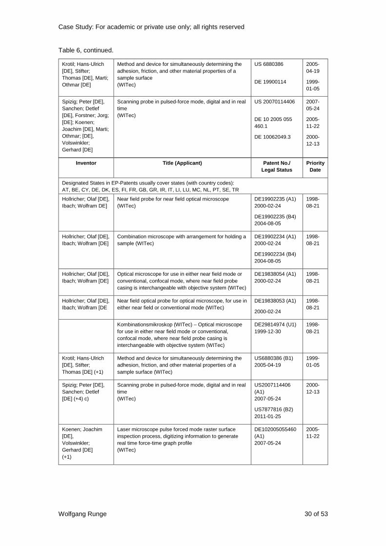
Case Study: For academic or private use only; all rights reserved
Wolfgang Runge 30 of 53
Table 6, continued.
Krotil; Hans-Ulrich [DE], Stifter; Thomas [DE], Marti; Othmar [DE]
Method and device for simultaneously determining the adhesion, friction, and other material properties of a sample surface (WITec)
US 6880386
DE 19900114
2005-04-19
1999-01-05
Spizig; Peter [DE], Sanchen; Detlef [DE], Forstner; Jorg; [DE]; Koenen; Joachim [DE], Marti; Othmar; [DE], Volswinkler; Gerhard [DE]
Scanning probe in pulsed-force mode, digital and in real time (WITec)
US 20070114406
DE 10 2005 055 460.1
DE 10062049.3
2007-05-24
2005-11-22
2000-12-13
Inventor Title (Applicant) Patent No./ Legal Status
Priority Date
Designated States in EP-Patents usually cover states (with country codes): AT, BE, CY, DE, DK, ES, FI, FR, GB, GR, IR, IT, LI, LU, MC, NL, PT, SE, TR
Hollricher; Olaf [DE], Ibach; Wolfram DE]
Near field probe for near field optical microscope (WITec)
DE19902235 (A1) 2000-02-24
DE19902235 (B4) 2004-08-05
1998-08-21
Hollricher; Olaf [DE], Ibach; Wolfram [DE]
Combination microscope with arrangement for holding a sample (WITec)
DE19902234 (A1) 2000-02-24
DE19902234 (B4) 2004-08-05
1998-08-21
Hollricher; Olaf [DE], Ibach; Wolfram [DE]
Optical microscope for use in either near field mode or conventional, confocal mode, where near field probe casing is interchangeable with objective system (WITec)
DE19838054 (A1) 2000-02-24
1998-08-21
Hollricher; Olaf [DE], Ibach; Wolfram [DE
Near field optical probe for optical microscope, for use in either near field or conventional mode (WITec)
DE19838053 (A1)
2000-02-24
1998-08-21
Kombinationsmikroskop (WITec) – Optical microscope for use in either near field mode or conventional, confocal mode, where near field probe casing is interchangeable with objective system (WITec)
DE29814974 (U1) 1999-12-30
1998-08-21
Krotil; Hans-Ulrich [DE], Stifter; Thomas [DE] (+1)
Method and device for simultaneously determining the adhesion, friction, and other material properties of a sample surface (WITec)
US6880386 (B1) 2005-04-19
1999-01-05
Spizig; Peter [DE], Sanchen; Detlef [DE] (+4) c)
Scanning probe in pulsed-force mode, digital and in real time (WITec)
US2007114406 (A1) 2007-05-24
US7877816 (B2) 2011-01-25
2000-12-13
Koenen; Joachim [DE], Volswinkler; Gerhard [DE] (+1)
Laser microscope pulse forced mode raster surface inspection process, digitizing information to generate real time force-time graph profile (WITec)
DE102005055460 (A1) 2007-05-24
2005-11-22
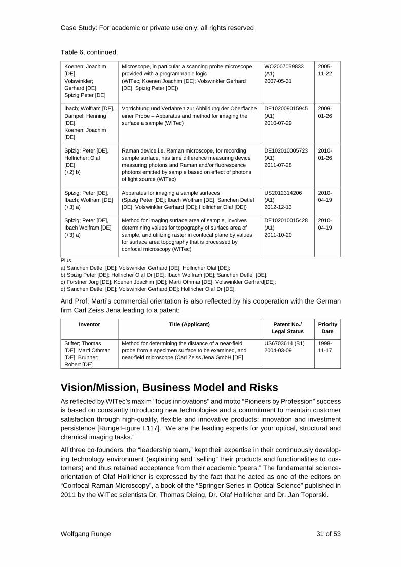
Case Study: For academic or private use only; all rights reserved
Wolfgang Runge 31 of 53
Table 6, continued.
Koenen; Joachim [DE], Volswinkler; Gerhard [DE], Spizig Peter [DE]
Microscope, in particular a scanning probe microscope provided with a programmable logic (WITec; Koenen Joachim [DE]; Volswinkler Gerhard [DE]; Spizig Peter [DE])
WO2007059833 (A1) 2007-05-31
2005-11-22
Ibach; Wolfram [DE], Dampel; Henning [DE], Koenen; Joachim [DE]
Vorrichtung und Verfahren zur Abbildung der Oberfläche einer Probe – Apparatus and method for imaging the surface a sample (WITec)
DE102009015945 (A1) 2010-07-29
2009-01-26
Spizig; Peter [DE], Hollricher; Olaf [DE] (+2) b)
Raman device i.e. Raman microscope, for recording sample surface, has time difference measuring device measuring photons and Raman and/or fluorescence photons emitted by sample based on effect of photons of light source (WITec)
DE102010005723 (A1) 2011-07-28
2010-01-26
Spizig; Peter [DE], Ibach; Wolfram [DE] (+3) a)
Apparatus for imaging a sample surfaces (Spizig Peter [DE]; Ibach Wolfram [DE]; Sanchen Detlef [DE]; Volswinkler Gerhard [DE]; Hollricher Olaf [DE])
US2012314206 (A1) 2012-12-13
2010-04-19
Spizig; Peter [DE], Ibach Wolfram [DE] (+3) a)
Method for imaging surface area of sample, involves determining values for topography of surface area of sample, and utilizing raster in confocal plane by values for surface area topography that is processed by confocal microscopy (WITec)
DE102010015428 (A1) 2011-10-20
2010-04-19
Plus a) Sanchen Detlef [DE]; Volswinkler Gerhard [DE]; Hollricher Olaf [DE]; b) Spizig Peter [DE]; Hollricher Olaf Dr [DE]; Ibach Wolfram [DE]; Sanchen Detlef [DE]; c) Forstner Jorg [DE]; Koenen Joachim [DE]; Marti Othmar [DE]; Volswinkler Gerhard[DE]; d) Sanchen Detlef [DE]; Volswinkler Gerhard[DE]; Hollricher Olaf Dr [DE].
And Prof. Marti’s commercial orientation is also reflected by his cooperation with the German firm Carl Zeiss Jena leading to a patent:
Inventor Title (Applicant) Patent No./ Legal Status
Priority Date
Stifter; Thomas [DE], Marti Othmar [DE]; Brunner; Robert [DE]
Method for determining the distance of a near-field probe from a specimen surface to be examined, and near-field microscope (Carl Zeiss Jena GmbH [DE]
US6703614 (B1) 2004-03-09
1998-11-17
Vision/Mission, Business Model and Risks As reflected by WITec’s maxim "focus innovations" and motto “Pioneers by Profession” success is based on constantly introducing new technologies and a commitment to maintain customer satisfaction through high-quality, flexible and innovative products: innovation and investment persistence [Runge:Figure I.117]. ”We are the leading experts for your optical, structural and chemical imaging tasks.”
All three co-founders, the “leadership team,” kept their expertise in their continuously develop-ing technology environment (explaining and “selling” their products and functionalities to cus-tomers) and thus retained acceptance from their academic “peers.” The fundamental science-orientation of Olaf Hollricher is expressed by the fact that he acted as one of the editors on “Confocal Raman Microscopy”, a book of the “Springer Series in Optical Science” published in 2011 by the WITec scientists Dr. Thomas Dieing, Dr. Olaf Hollricher and Dr. Jan Toporski.
Case Study: For academic or private use only; all rights reserved
Wolfgang Runge 32 of 53
Since 1997 WITec has emerged as an instrument and device fabrication and sales venture with intense R&D, innovation and IP protection activities and a sense of ur-gency to exhibit innovation and investment persistence for growth in rapidly developing industries/markets.
In addition to the core competencies of SNOM, Raman and AFM WITec continuously develops new competencies (cf. RISE microscope and StrobeLock, a time-correlated single photon counting (TCSPC) measurement option).
The focus on R&D in nanotechnology and materials research since around 2000 and life sciences industries, coupled with large governmental and corporate funding in this area, serves the market as a significant driver and was the major factor behind the constant growth of the market [Chai 2011]. Using an enabling technology for nanotechnology (nanotools) WITec took also advantage from current miniaturization in industry.
Concerning suppliers the WITec’s microscope systems require on the one hand self-developed mechanical parts and optical components that are made externally for WITec and on the other hand purchased parts from international markets. This requires WITec to have trustful relation-ships with it suppliers to secure a continuous stream of high quality purchased parts and, if needed, special customized parts.
Revenues are generated by sales of products and related product components, auxiliaries and complements (hard- and software), public grants for R&D projects and, to a minor degree, by education, training and other customer services. Accessories may include cantilevers, calibra-tion gratings, test samples and SNOM probes. Product components may include, for instance, specially prepared SNOM cantilevers, consisting of a silicon cantilever with a hollow aluminum pyramid as tip or a micro-fabricated SNOM sensor.
Mody [2011:159] in Chapter 5 (Commercialization in a Changing Community) cites an electrical engineer of the firm Digital Instruments (DI) who describes that sales “at least in a company that sells high tech instrumentation, actually involves a lot more people than the salesman. The salesman will make the contact and maybe open and close the deal, but he’ll also bring the person back and somebody from applications will run samples and get data. Maybe the guy’s going to have some technical questions, [so] he’ll talk to some engineers, and he’ll need new a feature added so he’ll talk to some software people. Basically a sale involves a bunch of people, not just a salesman, so why should that guy get a huge cut of a sale?”
Customer Orientation
Markets or customers, respectively, are from academics in universities, in public and industrial research institutes or laboratories from different scientific disciplines. “Industrial” also covers various fields (“customer segments”), such as polymer sciences, pharmaceuticals, biosciences, life science, geoscience, material sciences, thin films and coating analysis or semiconductors. All the investigated objects may be in various states (solid, liquid, and gaseous). Basically, a further dimension of products is temperature of the investigated objects, for instance, very low temperature, close to the absolute zero point (cf. Attocube Systems AG [Runge 2014b]).
WITec (as the other related companies Attocube and JPK Instruments) must know exactly the researchers’ mentality in scientific institutes and research and development departments. It should know which paths for support are available for scientists, how in the public sector finan-cial means will be approved or what requirements must be met in R&D departments of corpora-tions for new purchases. Being close to the target group is crucial for such manufacturers.
Purchasing in the public research fields may sometimes not be based on the budget or totally on the budget of the related organization. Here also the national science support organizations may play a role (NSF – National Science Foundation – in the US or the German Science Foundation (DFG – Deutsche Forschungsgemeinschaft)).
Case Study: For academic or private use only; all rights reserved
Wolfgang Runge 33 of 53
Customer-orientation is always re-emphasized and executed [Koenen 2010:9-10,14]. Corre-spondingly there are various, partially interwoven marketing and customer approaches [Koenen 2010].
Marketing and Customer Relationships comprise:
Gaining visibility:
• The Web (home page, YouTube) • Fairs, exhibitions, international scientific subject-related conferences or conferences of
scientific societies, such as the American Physical Society (APS) or its German coun-terpart (Deutsche Physikalische Gesellschaft – DPG),
• Congresses, meetings, events, • Advertisement (including covers of scientific journals with visualizations obtained with
an SPM of the related firm).
User Education and Training:
• Workshops, • Instrument demonstrations, • WITec Academy, • InFocus biannually newsletter, technical notes • WITec PaperAward (“Contribute your scientific results”).
Customer Contacts:
• Pre- and after-sales-service, sales and after-sales services by highly qualified scientific personnel,
• Customer visits, • User Meetings • Test measurements, • Customization of products, • Common projects.
Launching new products at key exhibitions/fairs/conferences (for instance, PITTCON in US, Analytica in Germany) is a marketing tool generating visibility, in particular focused visibility and reputation of the firm.
WITec Academy is a training program for all instrument and software operations as well as potential applications of the WITec product line.
The WITec PaperAward recognizes exceptional scientific publications based on results ob-tained with WITec microscopes. Scientists from all over the world are encouraged to submit their papers published in the ongoing year. Once a year, a jury will appoint the winner of this annual award.
Academic and industrial customers (basic segmentation) from the respective R&D environ-ments do not only have roles as partners in cooperation projects. In particular, academic cus-tomers play dual roles:
• Commercial role: end-users purchasing related offerings • The academic “customer as an innovator” (the user-innovator) for application develop-
ment – here the WITec PaperAward (Contribute your scientific results) will relate to new applications of WITec’s technologies or may report desirable improvements of products, and even first developments in this direction.
Pre-Sales service may play a similar role. Pre- and After-Sales service requires personnel with rather sophisticated technical knowledge and understanding.

Case Study: For academic or private use only; all rights reserved
Wolfgang Runge 34 of 53
WITec products (confocal Raman imaging/SPMs systems) are delivered worldwide to aca-demic and public and industrial research labs focusing on high-resolution chemical imaging and materials characterization.
Focusing to a large extent on customers from academia or public research is associated with relatively small markets which makes internationalization mandatory for a startup almost from the start.
A dedicated international market approach with an established service and support experience in the various regions of the world is one of WITec’s key strengths, evidenced by its widespread network of distributors and representatives as well as the US and Asian branch offices. In 2012 WITec further expanded its worldwide presence with the opening of regional offices in Japan and Spain (distribution channels). The US is one of WITec’s largest regional markets.
Subsidiaries and regional offices as in Japan and Spain will provide local sales support, pre-and after-sales service, organization of customer events and product demos.
WITec’s R&D activities rely to an important proportion on cooperative networking with its “home university”, but also other universities, public research institutes and also other companies. And also the overall research environment for communication and information sharing is important for technical developments. This is reflected when the Science Park II in Ulm was selected as a location of WITec’s building.
With the release of the first Confocal Raman Imaging system in 1999, WITec outperformed the existing Raman mapping techniques in terms of sensitivity, speed and lateral resolution, pioneering Raman spectroscopy as a tool for true 3D chemical imaging.
Raman spectroscopy and Confocal Raman Imaging represent a central core competency of WITec. The related central spectroscopic techniques supported and upgrade options cover
• Raman spectroscopy • Confocal Raman imaging • Ultrafast confocal Raman imaging • Topographic confocal Raman imaging • Confocal and near-field fluorescence spectroscopy • Upgradeable with atomic force (AFM) and near-field microscopy (SNOM) capabilities.
WITec’s modular product line approach does not only allow combination of WITec’s different microscopy technologies in one instrument, with corresponding measuring data processing and process control for comprehensive and flexible chemical, structural and optical analyses, but also integration with other (external) microscope technologies for further innovations, as the recent development of the RISE microscope shows which uses scanning electron microscopes (SEMs; Figure 3).
Generally, application development is not only focused on functionality and (users’) handlings of individual devices and their combination. WITec’s offerings are not a group of instruments, but an interwoven bunch of apparatuses, a system providing additional or enhanced functionali-ties outperforming those of the individual constituent instruments. Concepts in system func-tionality go for integration rather than interfacing.
Customers often seek for application that can be described as a set of interests related to wanted or required sequential tasks and activities, for instance, referring to different objects, needed functionalities and data management and visualization. Customers typically look for one individual instrument (they are most familiar with) for a job.
For instance, a question might be: What is the best AFM available in the market for both force measurements and high resolution imaging?

Case Study: For academic or private use only; all rights reserved
Wolfgang Runge 35 of 53
And the answer might be: It would depend on the application focusing on the desired results of the spectrum of tasks to be run. Say, the interest emphasizes the following aspects:
1. Imaging in liquid of biological samples 2. Force spectroscopy on material and ability to do imaging as well 3. Regular imaging.
Then, with these three requirements one can decide what kind of accessories or additions, respectively, or integration options to an AFM should be looked for.
WITec would be providing these methods within a single device. Also, a number of enhance-ments (“complements”) can be used to adapt WITec microscopes to meet customer require-ments, and they can be extended over time. WITec’s microscopes are not restricted to certain application areas; instead they are used broadly, for example, in materials science, nanotech-nology and medical research.
Developments and innovation of WITec does not only refer to instruments and their comple-ments (WITec as a supplier and also “complementor” [Runge:147]), but taking also the char-acteristics of samples or substrates, the objects of investigation, into account.
An example is WITec's recent TrueSurface microscopy technique which is available as an integrated option for the alpha300 microscope, but also available as an upgrade for installed alpha300 and alpha500 systems. Related systems measure the surface topography of large very rough or heavily inclined samples and correlates it with confocal Raman microscopy.
“Our customers have with every WITec system the possibility to undertake macroscopic inves-tigations along the surface of a sample on the millimeter-scale, while performing microscopic 3D Raman Imaging measurements on the sub-micron scale" explained Dr. Hollricher. "The pioneering integration of an optical profilometer in a Raman microscope opens for scientists new possibilities in surface analysis only offered in the modular WITec systems." [WITec 2012b]
WITec’s key elements and activities for product line extensions and new product development (“innovation objects”) are illustrated in Figure 4.
Figure 4: WITec’s key innovation elements and activities for product line extensions and new product development.
Concerning the future of optical measuring technology and image processing there is a noticea-ble trend towards 3D examinations and rendering of samples. This enables analysis of not only the properties on the surface of the sample, but also inside it. The results can then be displayed
Case Study: For academic or private use only; all rights reserved
Wolfgang Runge 36 of 53
and projected in 3D [Measurement Blog 2014]. A future direction is also Tip Enhanced Raman Spectroscopy (TERS).
Another increasingly important aspect for presentation of results is the ability to combine meas-urement results of different microscopy methods. The WITecProject software puts the firm in a strong position for all of this and it will be continuously developed.
According to its reporting (Elektronischer Bundesanzeiger – Electronic Federal Announce-ments) [EB]
• WITec sees itself as one of the globally leading producer of high-resolution optical and scanning probe microscopes.
• High priority goals of the firm are sustainable and profitable growth and extension of market leadership.
• The aim is also to further advance the development of leadership in the high-resolution optical and scanning probe microscopy.
Strategic objectives of WITec are:
• Leadership in technology and quality • Developing unique and innovative products • Global presence through expansion of sales efforts in core markets • Customer focus • Highly motivated employees.
WITec’s equity ratio is high 2008-2011 ca. 40 percent (27 percent in 2012; 2011: 43 percent, 2009: 39 percent, 2008: 41 percent) [EB].
According to WITec’s Dr. Spizig obvious critical success factors (CSFs) for the company are [Measurement Blog 2014]:
• Ingrained in history, WITec has strong interconnections with science and research (“ex-ternal networking”, “external resources”).
• WITec has always been, and will be focused on innovation and develop new technolo-gies that offers advantages to customers (innovation and investment persistence). For example, WITec has developed new sensor technology for near-field microscopes, in-troduced the first and to date the only combined Raman-AFM microscope to the mar-ket, and provides solutions covering confocal Raman microscopy on rough or uneven surfaces.
• Another advantage is certainly that all company departments, from development and production to sales and customer support, are located at the company headquarters in Ulm (“internal” networking”). This helps also to ensure maximum quality of products and customer service.
In addition it is important to note that, for innovation, WITec essentially focuses on the whole process of super-resolution microscopic investigation of objects and their materials and state/environment – from sample characteristics and preparation via running the task-oriented microscopic measurements, data collection and post-processing finalized by re-sults’ visualizations and presentation via an appropriate user-interface.
Over its seventeen years of existence WITec has developed and kept features of the class of German firms called Hidden Champions, the related features being listed by Runge [2013:ch. 4.4.1]. In particular, for WITec one observes:
Case Study: For academic or private use only; all rights reserved
Wolfgang Runge 37 of 53
• A long-term leadership team kept, specifically the CEO • Leaders (including CEO) with technical and commercial knowledge and expertise; have
contacts with customers • Persistence and continuous renewal of core competencies • A high degree of identification of owners and employees at all levels with the company • Team spirit at the company is as important as for soccer. The pride of the people work-
ing for the firm can be felt; interdisciplinary of development teams • Little fluctuation of employees, employee loyalty in R&D • Protection of technology; number of patents • Production of high-quality products totally or to more than 80 percent in Germany • There are always setbacks if a firm pursues long-term trends. And in this case it helps
Hidden Champions often that they put on great independence from banks.
Probe Microscopy and the Related Instrumental Community Between 1997 and 1999 there were many entrepreneurial activities in the AFM, SPM, STM and SNOM fields and startups were founded in various countries:
1997 Nanosurf AG (Switzerland) 1997 WITec GmbH (Germany) 1998 Triple-O Microscopy GmbH (Germany) 1998 Nanotec Electrónica SL (Spain) 1999 JPK Instruments AG (Germany) 1999 Asylum Research Corp. (US).
For instance, concerning SNOM an overview of research organizations involved in this tech-nology from 2002 lists 37 near-field optics research groups and networks [Hecht 2002]:
22 in Europe (with 16 from Germany or Switzerland) 12 from America 3 from Asia.
When dealing with competition in the AFM, SPM and SNOM fields it turns out that via persons there are many interrelations between the related startups.
Mody [2004; 2011; 2014] has analyzed the history of STM and AFM to develop the analytical concept of the “instrumental community” – a network of people who orient to some common interest in a technique or technology that can be used in research for measurement, charac-terization, imaging, etc.
As this is about a process of new technology development and also entrepreneurship it seems worthwhile to present a sketchy overview thereof.
In the current context of the firm WITec Prof. Othmar Marti, Experimental Physics Department Leader at the University of Ulm [Marti], as an “entrepreneurial professor” [Runge:267,305] helping and encouraging WITec’s foundation, plays a notable role.
Marti’s research interests cover: • Atomic Force Microscopy (AFM) • Scanning Near Field Optical Microscopy (SNOM) • X-ray structure determination.
Before becoming Professor of Experimental Physics at Ulm University there are several periods in his life, which were important for the development of second generation SPMs.

Case Study: For academic or private use only; all rights reserved
Wolfgang Runge 38 of 53
1983-1986 Doctoral Thesis: "Scanning Tunneling Microscope at Low Temperatures" Advisor: Dr. H. Rohrer, IBM Research, Rüschlikon, Switzerland, and Prof. J. Olsen, ETH Zürich
1986-1988 Postdoc, University of California, Santa Barbara., USA, Prof. P. K. Hansma Subject: Research on Scanning Force Microscopy of Biomaterials
1988 -1990 Researcher at ETH Zürich, Switzerland, in the group of Prof. J. Mlynek. Subject: Scanning Force Microscopy
1990-1994 Research Assistant, Physics Faculty, University of Konstanz, Germany, in the group of Prof. J. Mlynek Subject: Scanning force microscopy, scanning near-field optics and spec-troscopy, biomembranes, photorefractive materials, light induced forces.
Following Mody [2013; 2011] and using also the German JPK Instruments AG case (which includes also Triple-O) [Runge 2014a] Figure 5 provides a relationship map of the above men-tioned 1997-1999 startups as well as key involved persons and organizations.
Figure 5: European and US entrepreneurship in the AFM, STM, SPM, SNOM instrumental community (1997 – 1999).
The types of startups in Figure 5 include
• RBSUs in terms of university spin-outs (WITec, NanoSurf, Nanotec Electronica), also called “exploitation spin-outs” [Runge:168,193].
• Firms’ foundations by former employees of other firms (Asylum and Triple-O) and • One RBSU (JPK Instruments) which was founded originally by three students already
while performing their diploma theses in experimental physics or business administra-tion at the Humboldt University Berlin [Runge 2014a] can be classified as a “com-petence spin-out” [Runge:168,194].
Based on proximity of locations associated with spread of news and diffusion of knowledge about applied technology and firms’ foundations one is led to hypothesize rather weak links also to make NanoSurf and JPK Instruments part of the instrumental community.
Generally, the openness towards knowledge and open communication in the global interna-tional academic and research community and also the physical proximity of people in research organizations with an associated spread of knowledge and (business) ideas let the temporarily clustered occurrence of (RBSU) startups appear as “coincidence of ideas” in a particular field
Case Study: For academic or private use only; all rights reserved
Wolfgang Runge 39 of 53
– “being in the air.” A corresponding example has been described for the ionic liquids tech-nology [Runge:A.1.5] (relevant cases are also published).
Othmar Marti appears as a center with transatlantic edges (in the sense of in graph theory), particularly between Switzerland, the US and Germany and early interconnections to the roots of STM and AFM in the IBM Research Lab near Zurich. And during his 1983-1986 doctoral thesis with H. Rohrer from the IBM Lab as an advisor he may have had contacts with Prof. Arturo M. Baro from the Universidad Autónoma de Madrid (UAM) who spent his sabbatical 1983-84 at the IBM Research Lab.
Prof. Baro later became a founder of Nanotec Electronica together with Julio Gomez, Jose Maria Gomez and Jaime Colchero [Nanotec Electronica]. And with Jaime Colchero Marti cooperated when he was in Konstanz/Germany [Marti and Colchero 1995]. And contributing to a book on “Scanning Probe Microscopy Instrumentation” Marti also had, at least, rather weak ties to one editor of the book, Hans-Joachim Güntherodt, Professor of Experimental Physics at the University of Basel. More details on Nanotec are found in the JPK case [Runge 2014a].
Though Prof. Hansma from the University of California in Santa Barbara contributed to the development of the technology, he was not involved in firms’ foundation. Instead one of Hansma’s departmental colleagues, Virgil Elings, grasped the opportunity to found Digital Instruments (DI). Elings’ interest in the technique was awakened when he heard a talk at UCSB by Nicolás García from Madrid, also an early adopter of STM as a result of a sabbatical [Mody 2014].
DI was taken over by Veeco Instruments in 1998, but in 1999 several former DI-employees (partly from Hansma’s group) founded Asylum Research – conveying “the double entendre in its name that it would provide an asylum for disaffected Veeco employees.” [Mody 2011].
Another notable link from UMA to Switzerland in this context concerns Juan José Sáenz who is (Full) Professor at the Condensed Matter Department of UAM. In 1987 he obtained his PhD from UAM. During his post-doc, he worked on electron field emission from nanotips in Dr. H. Rohrer’s group at IBM-Zürich. He joined the UAM as Assistant Professor in 1982 and worked in Prof. N. García’s group. He was also involved in the first works on magnetic force microscopy (MFM) in collaboration with Prof. Güntherodt’s group in Basel [UAM].
One quintessence of Mody [2014] for his work on progress for scientific communities was a reference to Granovetter [1973] and his principle of “the strength of weak ties.”
Accordingly, “when scientists share strong ties with their colleagues – especially those from the same discipline and the same country – they possess a set of skills, knowledge, and contacts that is similar to those of the colleagues they are strongly tied to. Weak ties, by contrast, offer access to entirely new sets of skills, knowledge, and contacts – through colleagues in a different discipline, a different nation, a different kind of organizational setting (corporate versus aca-demic, for instance). Collaborations and exchanges between weakly tied colleagues allow each of them to bring something new back to the audiences to which they are strongly tied.”
Competition The markets for nanotools/scientific instruments covering ca. ten basically different technolo-gies [JETRO 2006] are characterized by few big companies, few medium-sized firms and several small firms, a “few big guys and a lot of little guys” [Anonymus 2003] – all with a global focus.
Competition does not occur only based on the same specific SPM technology, but will cover all technologies that have comparable functionalities and may be used for the same applications (“generic technologies”).
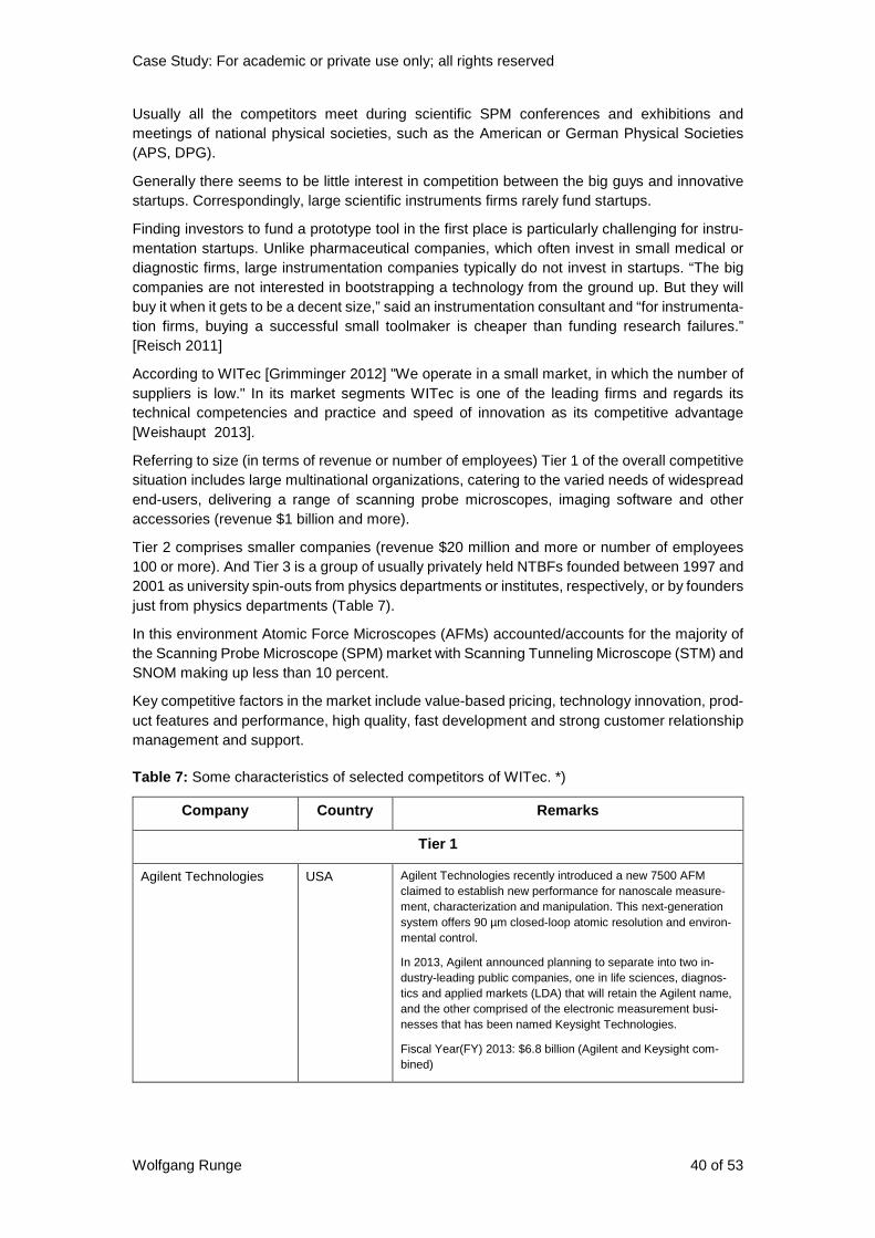
Case Study: For academic or private use only; all rights reserved
Wolfgang Runge 40 of 53
Usually all the competitors meet during scientific SPM conferences and exhibitions and meetings of national physical societies, such as the American or German Physical Societies (APS, DPG).
Generally there seems to be little interest in competition between the big guys and innovative startups. Correspondingly, large scientific instruments firms rarely fund startups.
Finding investors to fund a prototype tool in the first place is particularly challenging for instru-mentation startups. Unlike pharmaceutical companies, which often invest in small medical or diagnostic firms, large instrumentation companies typically do not invest in startups. “The big companies are not interested in bootstrapping a technology from the ground up. But they will buy it when it gets to be a decent size,” said an instrumentation consultant and “for instrumenta-tion firms, buying a successful small toolmaker is cheaper than funding research failures.” [Reisch 2011]
According to WITec [Grimminger 2012] "We operate in a small market, in which the number of suppliers is low." In its market segments WITec is one of the leading firms and regards its technical competencies and practice and speed of innovation as its competitive advantage [Weishaupt 2013].
Referring to size (in terms of revenue or number of employees) Tier 1 of the overall competitive situation includes large multinational organizations, catering to the varied needs of widespread end-users, delivering a range of scanning probe microscopes, imaging software and other accessories (revenue $1 billion and more).
Tier 2 comprises smaller companies (revenue $20 million and more or number of employees 100 or more). And Tier 3 is a group of usually privately held NTBFs founded between 1997 and 2001 as university spin-outs from physics departments or institutes, respectively, or by founders just from physics departments (Table 7).
In this environment Atomic Force Microscopes (AFMs) accounted/accounts for the majority of the Scanning Probe Microscope (SPM) market with Scanning Tunneling Microscope (STM) and SNOM making up less than 10 percent.
Key competitive factors in the market include value-based pricing, technology innovation, prod-uct features and performance, high quality, fast development and strong customer relationship management and support.
Table 7: Some characteristics of selected competitors of WITec. *)
Company Country Remarks
Tier 1
Agilent Technologies USA Agilent Technologies recently introduced a new 7500 AFM claimed to establish new performance for nanoscale measure-ment, characterization and manipulation. This next-generation system offers 90 µm closed-loop atomic resolution and environ-mental control.
In 2013, Agilent announced planning to separate into two in-dustry-leading public companies, one in life sciences, diagnos-tics and applied markets (LDA) that will retain the Agilent name, and the other comprised of the electronic measurement busi-nesses that has been named Keysight Technologies.
Fiscal Year(FY) 2013: $6.8 billion (Agilent and Keysight com-bined)

Case Study: For academic or private use only; all rights reserved
Wolfgang Runge 41 of 53
Table 7, continued.
JEOL Ltd. Japan Revenue 2011 $904,738 thousands; a manufacturer of electron microscopes and other scientific in-struments.
JEOL Ltd. has four business segments: Electron Optics manu-factures scanning electron microscopes, transmission electron microscopes and scanning probe microscopes, along with re-lated equipment. The Analytical Instruments section's products include mass spectrometers, nuclear magnetic resonance and electron spin resonance equipment.
Veeco Instruments Inc.
Veeco was the world's largest manufacturer of scanning probe micro-scopes;
SPM business acquired by German firm Bruker in 2010, run as Bruker Nano or Bruker Nano Surfaces.
USA
Germany
Revenue $980 million (FY 2011), ca. 900 employees; a large multi-technologies firm with a large emphasis on AFM; in 2010 Veeco’s atomic force microscope (AFM) business and its optical industrial metrology (OIM) business were sold to Bruker Nano. It also included Veeco’s associated global AFM/OIM field sales and support organization.
Claim: Bruker provides the critical surface measurements necessary for success with the world's broadest range of AFMs, stylus profilers, mechanical testers, non-contact 3D optical microscopes, and fluorescent microscopes.
Asylum Research Corp. acquired by Oxford Instruments company in 2012:
Asylum Research, an Oxford Instruments Company
USA
UK
Founded in 1999, revenue of $19.6 million (2011) [Photonics 2012], for an unknown year revenue is given as $13,249,800 with 32 employees [US Business Catalogue]; an employee-owned company;
focuses on AFM for both materials and bioscience applications; supports all major AFM/SPM scanning modes and capabilities with many exclusively advanced scanning modes for many dif-ferent applications; its first products were pico-Newton sensitive instruments for measuring the forces between and within molecules [Test&Measurement 2000]
Recently claimed to have reinvented tapping mode for remarka-bly more simple, stable, and quantitative imaging (“blueDrive”) – whether using tapping mode for high resolution topographical imaging in liquids, for elastic and loss moduli mapping on poly-mers, or on high-modulus materials.
Tier 2
NT-MDT Co. (Molecular Devices and Tools for NanoTechnology)
Russia Established in 1991; revenue $107.6 mio. (2010) [NT-MDT 2011b], in 2004 250 employees; focus on AFM; instrumentation and combining many technolo-gies created specifically for very wide areas of nanotechnology research.
In 2010 claimed to have installed more than 2,000 SPM sys-tems worldwide [NT-MDT 2010].
The application-focused instruments provide a range of capabili-ties in AFM-Raman, high-resolution, multi-frequency measure-ments, and AFM based nanomechanics.
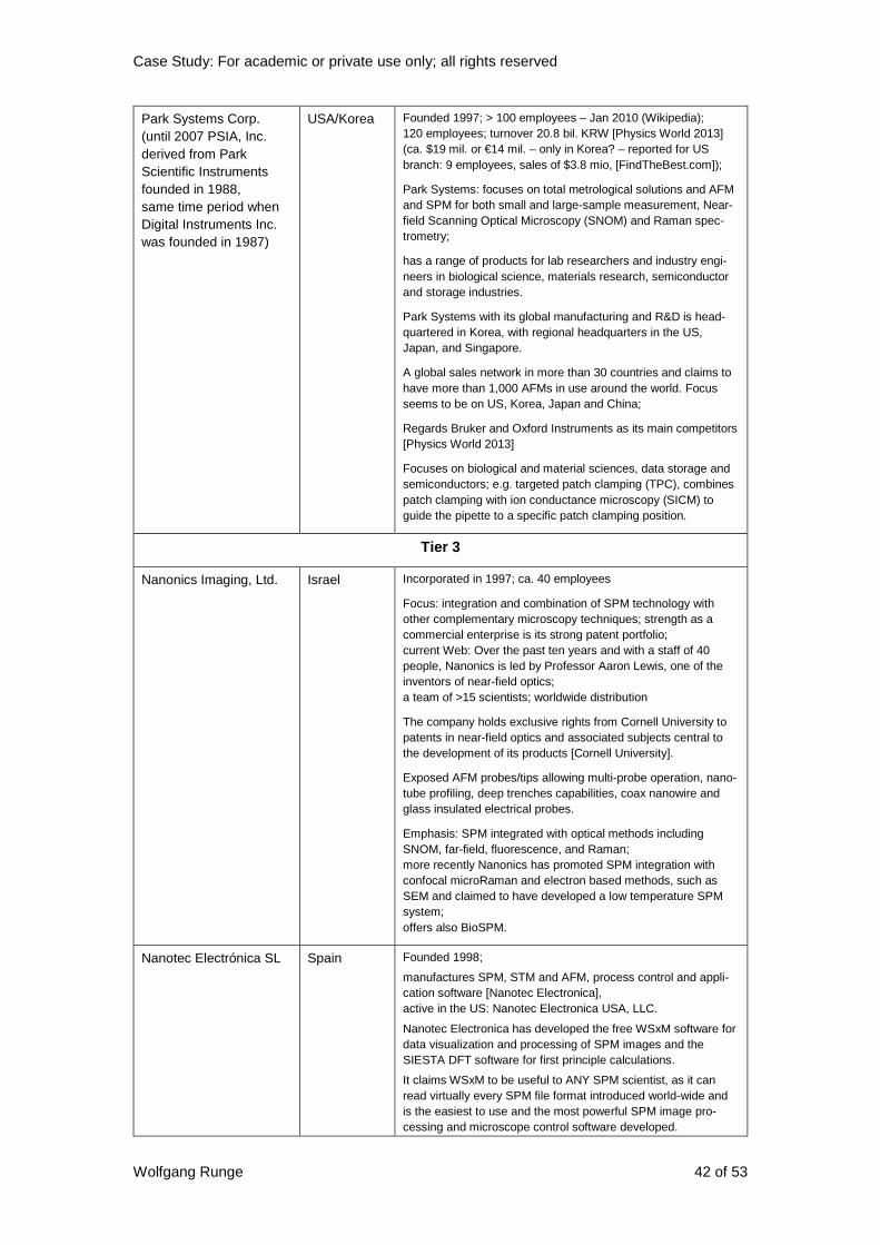
Case Study: For academic or private use only; all rights reserved
Wolfgang Runge 42 of 53
Park Systems Corp. (until 2007 PSIA, Inc. derived from Park Scientific Instruments founded in 1988, same time period when Digital Instruments Inc. was founded in 1987)
USA/Korea Founded 1997; > 100 employees – Jan 2010 (Wikipedia); 120 employees; turnover 20.8 bil. KRW [Physics World 2013] (ca. $19 mil. or €14 mil. – only in Korea? – reported for US branch: 9 employees, sales of $3.8 mio, [FindTheBest.com]);
Park Systems: focuses on total metrological solutions and AFM and SPM for both small and large-sample measurement, Near-field Scanning Optical Microscopy (SNOM) and Raman spec-trometry;
has a range of products for lab researchers and industry engi-neers in biological science, materials research, semiconductor and storage industries.
Park Systems with its global manufacturing and R&D is head-quartered in Korea, with regional headquarters in the US, Japan, and Singapore.
A global sales network in more than 30 countries and claims to have more than 1,000 AFMs in use around the world. Focus seems to be on US, Korea, Japan and China;
Regards Bruker and Oxford Instruments as its main competitors [Physics World 2013]
Focuses on biological and material sciences, data storage and semiconductors; e.g. targeted patch clamping (TPC), combines patch clamping with ion conductance microscopy (SICM) to guide the pipette to a specific patch clamping position.
Tier 3
Nanonics Imaging, Ltd. Israel Incorporated in 1997; ca. 40 employees
Focus: integration and combination of SPM technology with other complementary microscopy techniques; strength as a commercial enterprise is its strong patent portfolio; current Web: Over the past ten years and with a staff of 40 people, Nanonics is led by Professor Aaron Lewis, one of the inventors of near-field optics; a team of >15 scientists; worldwide distribution
The company holds exclusive rights from Cornell University to patents in near-field optics and associated subjects central to the development of its products [Cornell University].
Exposed AFM probes/tips allowing multi-probe operation, nano-tube profiling, deep trenches capabilities, coax nanowire and glass insulated electrical probes.
Emphasis: SPM integrated with optical methods including SNOM, far-field, fluorescence, and Raman; more recently Nanonics has promoted SPM integration with confocal microRaman and electron based methods, such as SEM and claimed to have developed a low temperature SPM system; offers also BioSPM.
Nanotec Electrónica SL Spain Founded 1998;
manufactures SPM, STM and AFM, process control and appli-cation software [Nanotec Electronica], active in the US: Nanotec Electronica USA, LLC.
Nanotec Electronica has developed the free WSxM software for data visualization and processing of SPM images and the SIESTA DFT software for first principle calculations.
It claims WSxM to be useful to ANY SPM scientist, as it can read virtually every SPM file format introduced world-wide and is the easiest to use and the most powerful SPM image pro-cessing and microscope control software developed.
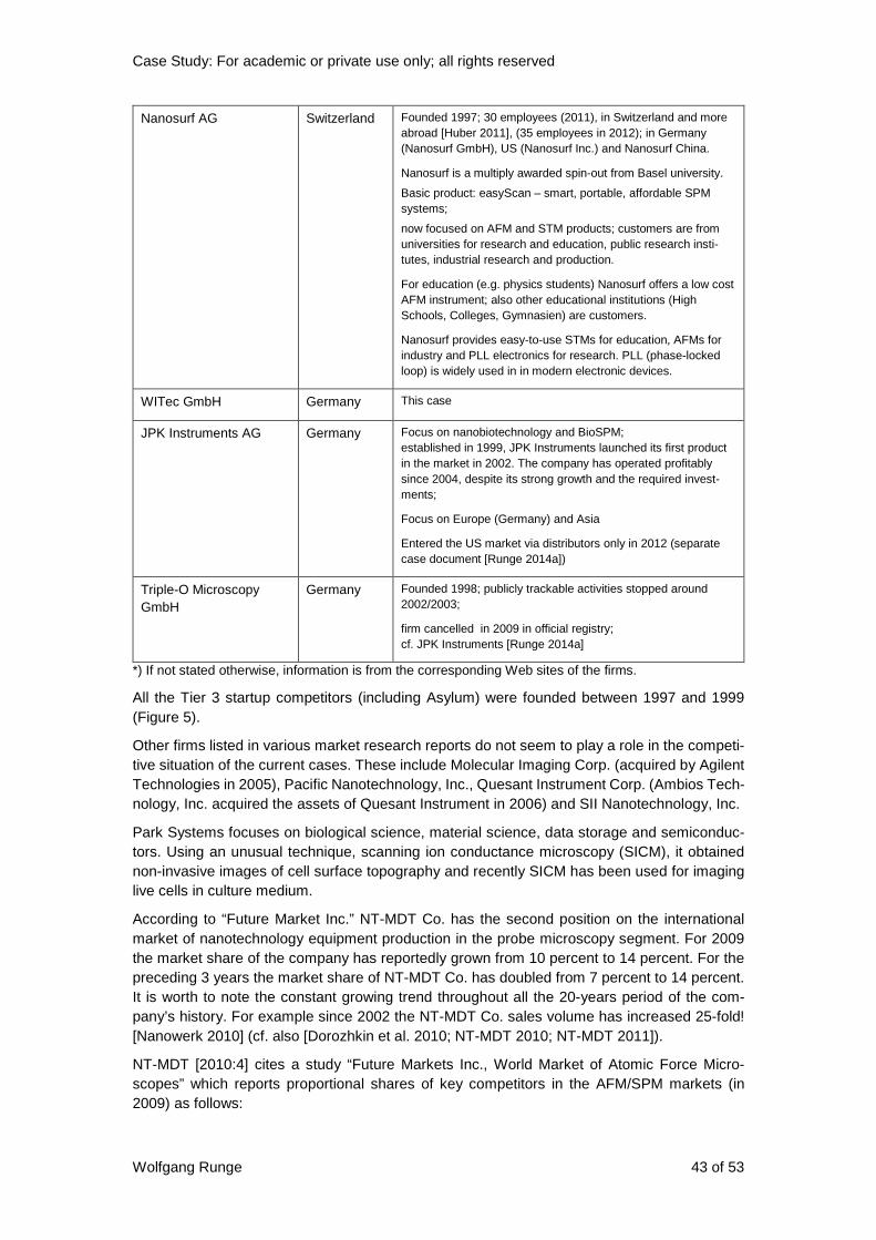
Case Study: For academic or private use only; all rights reserved
Wolfgang Runge 43 of 53
Nanosurf AG Switzerland Founded 1997; 30 employees (2011), in Switzerland and more abroad [Huber 2011], (35 employees in 2012); in Germany (Nanosurf GmbH), US (Nanosurf Inc.) and Nanosurf China.
Nanosurf is a multiply awarded spin-out from Basel university.
Basic product: easyScan – smart, portable, affordable SPM systems;
now focused on AFM and STM products; customers are from universities for research and education, public research insti-tutes, industrial research and production.
For education (e.g. physics students) Nanosurf offers a low cost AFM instrument; also other educational institutions (High Schools, Colleges, Gymnasien) are customers.
Nanosurf provides easy-to-use STMs for education, AFMs for industry and PLL electronics for research. PLL (phase-locked loop) is widely used in in modern electronic devices.
WITec GmbH Germany This case
JPK Instruments AG Germany Focus on nanobiotechnology and BioSPM; established in 1999, JPK Instruments launched its first product in the market in 2002. The company has operated profitably since 2004, despite its strong growth and the required invest-ments;
Focus on Europe (Germany) and Asia
Entered the US market via distributors only in 2012 (separate case document [Runge 2014a])
Triple-O Microscopy GmbH
Germany Founded 1998; publicly trackable activities stopped around 2002/2003;
firm cancelled in 2009 in official registry; cf. JPK Instruments [Runge 2014a]
*) If not stated otherwise, information is from the corresponding Web sites of the firms.
All the Tier 3 startup competitors (including Asylum) were founded between 1997 and 1999 (Figure 5).
Other firms listed in various market research reports do not seem to play a role in the competi-tive situation of the current cases. These include Molecular Imaging Corp. (acquired by Agilent Technologies in 2005), Pacific Nanotechnology, Inc., Quesant Instrument Corp. (Ambios Tech-nology, Inc. acquired the assets of Quesant Instrument in 2006) and SII Nanotechnology, Inc.
Park Systems focuses on biological science, material science, data storage and semiconduc-tors. Using an unusual technique, scanning ion conductance microscopy (SICM), it obtained non-invasive images of cell surface topography and recently SICM has been used for imaging live cells in culture medium.
According to “Future Market Inc.” NT-MDT Co. has the second position on the international market of nanotechnology equipment production in the probe microscopy segment. For 2009 the market share of the company has reportedly grown from 10 percent to 14 percent. For the preceding 3 years the market share of NT-MDT Co. has doubled from 7 percent to 14 percent. It is worth to note the constant growing trend throughout all the 20-years period of the com-pany’s history. For example since 2002 the NT-MDT Co. sales volume has increased 25-fold! [Nanowerk 2010] (cf. also [Dorozhkin et al. 2010; NT-MDT 2010; NT-MDT 2011]).
NT-MDT [2010:4] cites a study “Future Markets Inc., World Market of Atomic Force Micro-scopes” which reports proportional shares of key competitors in the AFM/SPM markets (in 2009) as follows:
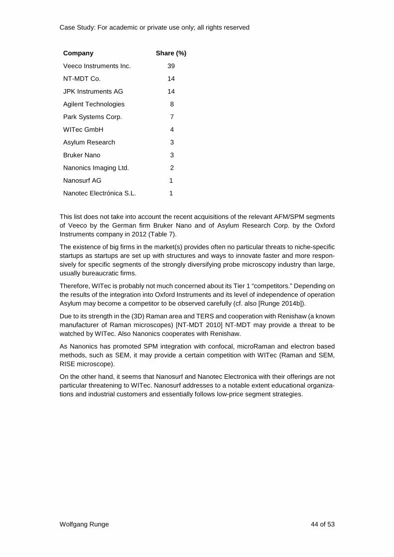
Case Study: For academic or private use only; all rights reserved
Wolfgang Runge 44 of 53
Company Share (%)
Veeco Instruments Inc. 39
NT-MDT Co. 14
JPK Instruments AG 14
Agilent Technologies 8
Park Systems Corp. 7
WITec GmbH 4
Asylum Research 3
Bruker Nano 3
Nanonics Imaging Ltd. 2
Nanosurf AG 1
Nanotec Electrónica S.L. 1
This list does not take into account the recent acquisitions of the relevant AFM/SPM segments of Veeco by the German firm Bruker Nano and of Asylum Research Corp. by the Oxford Instruments company in 2012 (Table 7).
The existence of big firms in the market(s) provides often no particular threats to niche-specific startups as startups are set up with structures and ways to innovate faster and more respon-sively for specific segments of the strongly diversifying probe microscopy industry than large, usually bureaucratic firms.
Therefore, WITec is probably not much concerned about its Tier 1 “competitors.” Depending on the results of the integration into Oxford Instruments and its level of independence of operation Asylum may become a competitor to be observed carefully (cf. also [Runge 2014b]).
Due to its strength in the (3D) Raman area and TERS and cooperation with Renishaw (a known manufacturer of Raman microscopes) [NT-MDT 2010] NT-MDT may provide a threat to be watched by WITec. Also Nanonics cooperates with Renishaw.
As Nanonics has promoted SPM integration with confocal, microRaman and electron based methods, such as SEM, it may provide a certain competition with WITec (Raman and SEM, RISE microscope).
On the other hand, it seems that Nanosurf and Nanotec Electronica with their offerings are not particular threatening to WITec. Nanosurf addresses to a notable extent educational organiza-tions and industrial customers and essentially follows low-price segment strategies.
Case Study: For academic or private use only; all rights reserved
Wolfgang Runge 45 of 53
References Anonymus (2014): Global Scanning Probe Microscopes (SPM) Market Analysis. Before It’s News, Jan. 30, 2014. http://beforeitsnews.com/business/2014/01/global-scanning-probe-microscopes-spm-market-analysis-2580206.html (last access 6/29/2014).
Anonymus (2003): Nanoscience Instruments sees gold in microscopy tools. Smalltimes, Nov. 3, 2003. http://www.smalltimes.com/articles/article_display.cfm?Section=ARCHI&C=Profi&ARTICLE_ID=269070&p=109 (no longer accessible, cf. http://electroiq.com/blog/2003/11/nanoscience-instruments-sees-gold-in-microscopy-tools/ accessed on 6/30/2014).
BioPro (2010a): Angelika Rück macht den Tanz der Moleküle sichtbar (Angelika Rück makes visible the dance of molecules). BioPro, Oct. 25, 2010. http://www.bio-pro.org/standort/aktuelle_forschung_in_bw/portraet/index.html?lang=de&artikelid=/artikel/05643/index.html (last access 12/18/2010).
Bio-Pro (2010b): Ulmer Hochzeit: WITec übernimmt Mehrheit an omt (Marriage in Ulm: WITec takes over omt). Bio-Pro Magazine, Aug. 25, 2010. http://www.bio-pro.de/magazin/wirtschaft/index.html?lang=de&artikelid=/artikel/05543/index.html (last access 4/25/2011).
BMBF – Federal Ministry of Education and Research (2007): Projekt: Automatisierte multidimensionale Gewebediagnostik zur Verbesserung von Prognoseinschätzung und Therapieempfehlung bei Krebserkrankungen – Exprimage (Automated multi-dimensional tissue-based diagnostics to improve forecasting estimates .and recommended therapy in cancer). http://www.photonikforschung.de/fileadmin/Verbundsteckbriefe/1._Bio/Verbund_Steckbrief_Exprimage.pdf; cf. also http://www.biophotonik.org/files/broschuere-biophotonik_2.pdf (last access 11/28/2009).
Chai, C. (2011): Global Microscopes Market Expected to Grow to More Than $9 Billion by 2017. Azonano, Aug. 27, 2011. http://www.azonano.com/news.aspx?newsID=23292 (last access 6/29/2014).
ChemEurope.com (2012): Photonics Innovation Award for WITec – True Surface Microscopy wins Photonics Prism Award 2011. Published Feb. 2, 2012. http://www.chemeurope.com/en/news/136293/photonics-innovation-award-for-witec.html (last access 4/27/2012).
Cornell University: Nanonics Imaging Ltd. CCTEC. http://smallbizdev.cornell.edu/companies/nanonics-imaging-ltd (last access 5/20/2013).
Deutscher Gründerpreis (2007): Einsatz im Kometenstaub (Use for comet dust). http://www.deutscher-gruenderpreis.de/owx_medien/media11/1196.pdf (last access 7/23/2009), no longer accessible.
Dorozhkin, P., Kuznetsov, E.; Schokin, A.; Timofeev, S.; Bykov, V. (2010): AFM + Raman Microscopy + SNOM + Tip-Enhanced Raman: Instrumentation and Applications. Microscopy Today 18, p. 28-32. doi:10.1017/S1551929510000982.
Emes, M. (2005): Market Landscape: the Myth and the Reality. UCL Mullard Space Science, Laboratory, September 2005. https://wwws.ee.ucl.ac.uk/students/postgraduate/masters/mscnano/marketlandscape.pdf (last access 8/23/2009), no longer accessible.

Case Study: For academic or private use only; all rights reserved
Wolfgang Runge 46 of 53
FES – Friedrich Ebert Stiftung (1998): 4. Finanzierung als ein zentrales Gründerproblem, 4.1 Bankenfinanzierung und öffentliche Fördermittel – Das Problem der Sicherheiten (Bank financing and public funding – The problem of collateral). Ulm, Nov. 16 1998. http://library.fes.de/fulltext/fo-wirtschaft/00948005.htm (last access 10/5/2009).
FindTheBest.com: Park Systems, Inc in Santa Clara CA. http://companies.findthebest.com/l/14343284/Park-Systems-Inc-in-Santa-Clara-CA (last access 2/23/2014).
Firmenpresse (2009): Neue WITec Firmenzentrale (New WITec Headquarters). Firmenpresse, Jun. 25, 2009. http://www.firmenpresse.de/pressinfo98190.html (last access 12/3/2009).
Fischer, H. (2006): WITec has launched the new alpha300 microscope generation. Nanotechnology Now, posted on March 9, 2006. http://www.nanotech-now.com/news.cgi?story_id=14147 (last access 9/29/2009).
Future Markets Inc. (2014): Scanning Probe Microscopes: The Global Market. Jan. 1, 2014. http://www.marketresearchreports.biz/analysis/190812 (last access 6/23/3014).
Future Markets (2011): The World Market for Atomic Force Microscopes and Afm Probes. Published Date 2011-01-01. http://www.researchmoz.com/the-world-market-for-atomic-force-microscopes-and-afm-probes-report.html (last access 6/29/2014).
Granovetter, M. S. (1973): The Strength of Weak Ties. American Journal of Sociology 78 (6), 1360-1380. https://sociology.stanford.edu/sites/default/files/publications/the_strength_of_weak_ties_and_exch_w-gans.pdf; cf. also http://www.soc.ucsb.edu/faculty/friedkin/Syllabi/Soc148/Granovetter%201983.pdf (last access 8/31/2014).
Grimminger, R. (2012): WITec – Marktführer mit speziellen Mikroskopen (WITec – Market leader with special microscopes). Ulm News, Mar. 14, 2012. http://www.ulm-news.de/weblog/ulm-news/view/dt/3/article/12401/WItec_-_Marktf-uuml-hrer_mit_speziellen_Mikroskopen.html (last access 7/30/2012).
Hecht, B. (2002): NFO Research groups and networks. Near-Field Optics online, Aug. 28, 2002. http://www.nano-optics.ch/nfo_online/research.html (last access 10/2/2014).
Hessen – Hessisches Ministerium für Wirtschaft, Verkehr und Landesentwicklung (2009): NanoAnalytik – Anwendung in Forschung und Praxis (Nano-Analytics – Application in Research and Praxis). December 2009. http://www.hessen-nanotech.de/mm/NanoAnalytik_Anwendung_Praxis_Forschung_web.pdf (last access 5/18/2010).
Hollricher, O. (2003): Combine & Conquer – Confocal Raman microscopy teams high-resolution capabilities with powerful materials analysis; Many paths lead to a microscopy expert. From oemagazine, Nov. 31, 2003, SPIE Newsroom. http://spie.org/x17652.xml?ArticleID=x17652 (last access 7/13/2009).
Huber, L. (2011): Auf den Mars (To the Mars). Volksstimme, Sep. 22, 2011. http://pdf.volksstimme.ch/vsspez/wirtschaft/standortbaselbiet_2011.09.22.pdf (last access 3/17/2012), no longer accessible.
IHK (2010): WITec GmbH, Ulm. IHK Ulm und IHK Bodensee-Oberschwaben; Die Wirtschaft, 7-8/2010. http://www.wab.ihk.de/index.php?id=22569 (last access 5/26/2011).
Case Study: For academic or private use only; all rights reserved
Wolfgang Runge 47 of 53
Imaging & Microscopy (2014): WITec Suite Software: High-Speed Data Acquisition and Processing of Large Data Volumes for Raman, AFM, and SNOM. Imaging & Microscopy, Jun. 10, 2014. http://www.imaging-git.com/products/scanning-probe-microscopy/witec-suite-software-high-speed-data-acquisition-and-processing-l (last access 7/5/2014).
Imaging & Microscopy (2013): StrobeLock: A Time-Correlated Single Photon Counting Measurement Option. Imaging & Microscopy, Mar. 25, 2013. http://www.imaging-git.com/products/light-microscopy/strobelock-time-correlated-single-photon-counting-measurement-option (last access 6/24/2013).
Jamison, D. W. (2003): Who’s getting the cash in nanomanufacturing? File of 5/28/2003. http://web.mit.edu/nanosymposium/www/Presentations/jamison.pdf (5/16/2011).
JETRO (2006): Nanoscale Equipment for Visualization and Measurement. Japanese Market Report, No. 77, March 2006. http://www.jetro.go.jp/en/reports/market/pdf/2006_08_b.pdf (last access 2/23/2009).
Kassing, R.; Oesterschulze, E. (2001): Sonden für Lichtmikroskopie mit 40 Nanometern Auflösung entwickelt und serienfertig – Entwicklung der Kasseler Nanotechnologie ist Durchbruch für die Lichtmikroskopie (Probes for light microscopy with 40 nanometer resolution developed and ready for production in series – Development of Kassel nanotechnology is breakthrough for light microscopy). Press Release Uni Kassel, 132/01 – 23. November 2001. http://www.uni-kassel.de/presse/pm/archiv/nov01-10.ghk?style=print (last access 10/31/2009).
Koenen, J. (2010): Unternehmer? Warum nicht! (Entrepreneur? Why not!). Presentation Technology Entrepreneurship, Jan. 27, 2010. http://ce.ioc.kit.edu/downloads/Praesentation_Koenen.pdf.
Marti, O.: Curriculum Vitae. http://wwwex.physik.uni-ulm.de/marti/.
Marti, O.; Colchero, J. (1995): Scanning Probe Microscopy Instrumentation. In H. J. Güntherodt, D. Anselmetti, E. Meyer (Eds.): Forces in Scanning Probe Methods, NATO ASI Series Volume 286, 1995, p. 15-34. http://link.springer.com/chapter/10.1007/978-94-011-0049-6_2 (last access 6/2/2010).
Measurement Blog (2014): 5 questions for Dr. Spizig. Measurement Blog, Jan. 5, 2014. http://blog.micro-epsilon.com/2014/01/5-questions-for-dr-spizig/ (last access 3/23/2014).
Mody, C. C. M. (2004): Crafting the Tools of Knowledge: The Invention, Spread, and Commercialization of Probe Microscopy, 1960-2000. Dissertation, Faculty of the Graduate School of Cornell University, August 2004. http://www.owlnet.rice.edu/~Cyrus.Mody/MyPubs/crafting.pdf (last access 5/4/2014).
Mody C. C. M. (2011): Instrumental Community: Probe Microscopy and the Path to Nanotechnology. MIT Press, Cambridge, Mass, 2011.
Mody, C. C. M. (2014): Probe microscopy: a transdisciplinary and transatlantic instrumental community. In BUNSEN MAGAZIN 16, 5/2014, p. 214-210. http://www.bunsen.de/bunsen_media/BuMa_2014_05-p-1392.pdf (last access 8/31/2014).
Nanotec Electronica: Web site. http://www.nanotec.es/, http://www.nanotec.es/about_us/index.php (last access 6/17/2014).
Nanowerk (2010): NT-MDT Was The Highest-Growth Company In The SPM Market In 2009. Nanowerk, posted March 5, 2010. http://www.nanowerk.com/news/newsid=15180.php (last access 6/29/2014).
Case Study: For academic or private use only; all rights reserved
Wolfgang Runge 48 of 53
Nanowerk (2009): New Chemometric Software for Raman Spectral and Microscopic Data Analysis. Nanowerk, posted March 20, 2009. http://www.nanowerk.com/news/newsid=9720.php (last access 9/14/2009).
Nanowerk (2007): Automated 3-D Chemical Imaging Combined with AFM. Nanowerk Business News, posted November 29, 2007. http://www.nanowerk.com/news/newsid=3498.php (last access 12/1/2014).
NT-MDT (2011a): The breakthrough to the American market. Press Release, Jan. 27, 2011. http://www.ntmdt.com/press-releases/view/kachestvennyj-proryv-na-amerikanskom-rynke (last access 6/29/2014).
NT-MDT (2011b): Instrumentation for Nanotechnology. NT-MDT Company Presentation, on Jan. 26, 2011. http://de.slideshare.net/NTMDT/nt-mdt-companypresentation-2011-nl (last access 6/23/2012).
NT-MDT (2010): AFM – Raman – SNOM and Tip Enhanced Raman Instrumentation and Applications. Outlook: 1. AFM – Raman – SNOM – TERS instrumentation. File of 9/23/2010. Google Search “AFM – Raman – SNOM and Tip Enhanced Raman” provides access to PDF-file of 9/23/2010. https://www.google.de/url?sa=t&rct=j&q=&esrc=s&source=web&cd=2&cad=rja&uact=8&ved=0CEsQFjAB&url=http%3A%2F%2Fwww.ntmdt.com%2Fdata%2Fmedia%2Ffiles%2Fproducts%2Fntegra%2Fntegra_spectra_applications.pdf&ei=AIWxU-e2KcGmPczRgPAN&usg=AFQjCNHAI72Np9DXiCPGwjVB5f44Blk4JQ&bvm=bv.69837884,d.bGE.
NanUUU (2014): Nanostrukturen auf der Spur: EU fördert die Entwicklung korrelativer Mikroskopietechniken (Tracking nano-structures. EU supports the development of correlative microscopy techniques). NanUUU, Apr. 2, 2014. http://www.nanuuu.de/nanostrukturen-auf-der-spur-eu-foerdert-die-entwicklung-korrelativer-mikroskopietechniken/ (last access 5/19/2014).
Photonics (2012): Oxford Instruments Acquires Asylum Research for Up to $80M. Published Dec. 17, 2012. http://www.photonics.com/Article.aspx?AID=52601 (last access 2/4/2013).
PhotonicsBW (2010): Das Kompetenznetzwerk für Optische Technologien in Baden-Württemberg (The Competence Network for Optical Technologies in Baden-Württemberg). http://extern.htw-aalen.de/zafh/Photoniktag2010/ZAFH_Photoniktag_2010_Erhardt.pdf (last access 2/7/2011).
PITTCON (2013): The Twenty-Fourth James L Waters Annual Symposium: Chemical Imaging Spectroscopy. PITTCON, March 17 - 21, 2013, Philadelphia, PA, USA. http://vault.pittcon.org/2013/technical-program/waters-symposium/index.html (last access 11/27/2013).
Phys.org (2005): Nanotech tools a $700M market. Phys.org, Jul. 20, 2005. http://www.physorg.com/news5307.html (last access 1/26/2009).
Physics World (2013): Small Firms Fight Hard – Smaller Hi-tech Firm Case Study Featuring Park Systems. Physics World, September 2013. http://www.parkafm.com/index.php/medias/news/press-release/39-small-firms-fight-hard-smaller-hi-tech-firm-case-study-featuring-park-systems-physics-world-september-2013 (last access 1/23/2014).
PresseEcho (2010): Auf nach Russland! Geschäfte von morgen mit Technologien der Zukunft (Off to Russia! Tomorrow's business with technologies of the future). PresseEcho, Oct. 12, 2010. http://www.presseecho.de/wirtschaft/PE12868779417437.htm (last access 5/25/2011).
Case Study: For academic or private use only; all rights reserved
Wolfgang Runge 49 of 53
R&D Magazine (2011): Confocal stays true to the surface. R&D Magazine, Aug.14, 2011. http://www.rdmag.com/award-winners/2011/08/confocal-stays-true-surface (last access 3/23/2012).
Reisch, M. S. (2011): Instrumental Efforts – Entrepreneurs take big risks to bring the latest scientific tools to market. Chemical & Engineering News 89 (32), 14-19. http://pubs.acs.org/cen/coverstory/89/8932cover.html?featured=1 (last access 8/9/2011).
Research and Markets (2013): The Advanced Functional Material Market Growing with a CAGR of 6.6% is Expected to Generate Global Revenue of $1,13,881.9 Million by 2018. BusinessWire, Aug. 9, 2013. http://www.businesswire.com/news/home/20130809005587/en/Research-Markets-Advanced-Functional-Material-Market-Growing#.U7AFe_mSwXw (last access 6/29/2014).
Research and Markets (2011): The World Market for Atomic Force Microscopes (AFMs) and AFM Probes 2011. Published January 2011. http://www.researchandmarkets.com/reports/1543361/the_world_market_for_atomic_force_microscopes (last access 6/29/2014).
Rose, M. (2011): 2011 Prism Award Winners Announced. Photonics.com, January 2012. http://www.photonics.com/Article.aspx?AID=49873 (last access 2/9/2011).
Runge, W. (2014a): JPK Instruments AG. http://etm.entechnon.kit.edu/454.php.
Runge, W. (2014b): Attocube Systems AG. http://etm.entechnon.kit.edu/454.php.
Schäfer, M. (2009): Der Krebs muss Farbe bekennen (Cancer must show its colors). Baden-Württemberg Stiftung – Bild der Wissenschaft plus, Nov. 7, 2009, p. 42-43. http://www.bwstiftung.de/uploads/tx_ffbwspub/bdw_lichtblicke.pdf (last access 2/9/2010).
Spizig, P.; Sanchen, D.; Volswinkler, G.; Ibach, W.; Koenen, J. (2005). Alpha Control – A new concept in SPM Control. MAR06 Meeting of the American Physical Society, Nov. 30, 2005. http://absimage.aps.org/image/MAR06/MWS_MAR06-2005-004671.pdf (last access 1/29/2009).
TechNavio: The electron microscope market set to advance with other global technology industries. http://www.technavio.com/blog/electron-microscope-market-set-advance-other-global-technology-industries (last access 5/30/2014).
The Info Shop (2005): Nanotechnology for Photonics. Pub Time 2005/03. http://www.the-infoshop.com/study/bc27181_nanotech_photonics.html (last access 2/6/2009).
Test&Measurement (2000): Company Profile – Asylum Research. Published Dec. 21, 2000. http://www.testandmeasurement.com/doc/asylum-research-0001 (last access 5/30/2014).
Transparency Market Research (2014): Microscopy Devices Market [Products (Optical Microscopes, Electron Microscopes, Scanning Probe Microscopes and Others) and Applications (Semiconductors, Life Sciences, Nanotechnology, Material Sciences and Others) – Global Industry Analysis, Size, Share, Growth, Trends and Forecast, 2014 – 2020). Published Date: 2014-07-03. www.transparencymarketresearch.com/microscopy-market.html; http://photonics.com/Article.aspx?AID=54877 (last access 6/29/2014).
UAM - Universidad Autónoma de Madrid: Prof. Juan José Sáenz. http://www.uam.es/gruposinv/MoLE/page/quien/juanjo_uk.html (last access 5/22/2014).
Universität Ulm (2000a): Die Mutigen (The brave). Aktuelles Thema, March 2000. http://www.gruenderverbund-ulm.de/GVU2.html (last access 6/12/2008).
Case Study: For academic or private use only; all rights reserved
Wolfgang Runge 50 of 53
Universität Ulm (2000b): Schulbuchmäßige Firmengründung – Ulmer Experimentalphysiker als Jungunternehmer (Textbook-like Firm’s Foundation – Experimental physicists as Junior Entrepreneurs). In: Lebensstile und Nachhaltigkeit – Frühjahrsakademie des Zentrum für Allgemeine Wissenschaftliche Weiterbildung (ZAWiW), Mar., 30 – Apr. 3, 1998. http://vts.uni-ulm.de/docs/2000/423/vts_423.pdf (last access 6/23/2009).
Universität Ulm (1999): Kombi-Präzisionsmikroskop (Combined precision microscope). Uni Ulm Intern, January 1999. http://www.uni-ulm.de/uui/1999/nr226.htm (last access 11/23/2009).
Universität Ulm (1997): Pulsed Force GmbH – Ulmer Experimentalphysiker als Existenzgründer (Pulsed Force LLC – Experimental Physicists as Entrepreneurs). Uni Ulm Intern, November 1997. http://www.uni-ulm.de/uui/1997/int1197.htm (last access 6/25/2009).
Universität Ulm: Liste der abgeschlossenen Diplomarbeiten – Koenen, Joachim 1987 Heterogene Deformation polymerer Gläser (Heterogeneous deformation of polymeric glasses). http://wwwex.physik.uni-ulm.de/Arbeiten/Diplarb.htm (last access 10/31/2009); Liste der Dissertationen – Koenen, Joachim 1991 Vollständige Energiebilanz bei heterogener Kaltverformung von polymeren Gläsern (Complete energy balance in heterogeneous cold deformation of polymeric glasses). Weishaupt, Klaus 1995 Brillouinspektroskopie an polymeren Gläsern unter hohem Druck (Brillouin spectroscopy of polymeric glasses under high pressure). http://wwwex.physik.uni-ulm.de/Arbeiten/Diss.htm (last access 10/31/2009).
US Business Catalogue: Asylum Research. http://411dir.biz/1045018_california_goleta.html (last access 5/26/2014).
Von Bubnoff, A. (2007): How Germany nurtures its nanotech industry. Small Times, May/June 2007. http://www.smalltimes.com/display_article/292540/109/ARTCL/none/Feats/How_Germany_nurtures_its_nanotech_industry/ (last access 1/22/2009)); cf. also http://static.squarespace.com/static/52006112e4b0748af59ec135/t/530fc3dee4b0a73d96236dc8/1393542110645/German%20nanotech%20USE%20THIS.pdf.
Wani, P. (2013): Electron Microscopes for Nano-level Research – Market Insights. europlat.org, Jul. 15, 2013. http://www.europlat.org/electron-microscopes-for-nano-level-research-market-insights.htm (last access 6/23/2014).
Weishaupt, K. (2013): Wettbewerbsvorteil durch technologische Kompetenz – Innovation in der Praxis (Competitive advantage by technological competence – Practicing innovation). Vortrag (Lecture), Gründerverbund Ulm, Nov. 25, 2013. http://www.gruenderverbund-ulm.de/Programm_Hochschule_trifft_Wirtschaft.pdf (last access 3/25/2014).
Wikipedia-1: Monthly average of the US dollar/Yen spot rate (Yen per USD). http://en.wikipedia.org/wiki/Japanese_yen.
WITec (2014): History & Awards, About WITec. http://www.witec.de/company/ (last access 6/23/2014); http://www.witec.de/products/, http://www.witec.de/company/news-archive/.
WITec (2014a): TESCAN ORSAY HOLDING, a.s. and WITec GmbH launch the RISE Microscope for Correlative Raman-SEM Imaging at Analytica 2014. WITec News March 2014. http://www.witec.de/company/news-archive/2014/tescan-and-witec-launch-the-rise-microscope-for-correlative-raman-sem-imaging/ (last access 5/29/2014).
WITec (2014b): New software provides uncompromising performance, speed, and usability for Raman, AFM, and SNOM. WITec News May 2014. http://www.witec.de/company/news-archive/2014/new-software-provides-uncompromising-performance-speed-and-usability-for-raman-afm-and-snom/ (last access 6/16/2014).
Case Study: For academic or private use only; all rights reserved
Wolfgang Runge 51 of 53
WITec (2013a): WITec Managing Director contributes to The James L. Waters Annual Symposium on “Chemical Imaging Spectroscopy” at Pittcon Conference 2013. PITTCON Conference & Expo, Philadelphia, March 17-21, 2013. http://www.witec.de/company/news-archive/2013/witec-managing-director-contributes-to-the-james-l-waters-annual-symposium-at-pittcon/ (last access 8/26/2013).
WITec (2013b): PITTCON 2013: WITec launches StrobeLock for time-resolved measurements. WITec News March 2013. http://www.witec.de/company/news-archive/2013/pittcon-2013-witec-launches-strobelock-for-time-resolved-measurements/ (last access 6/23/2013).
WITec (2012a): International WITec Distributor Meeting 2012. WITec News February 2012. http://www.witec.de/company/news-archive/2012/international-witec-distributor-meeting-2012/ (last access 5/23/2013).
WITec (2012b): TrueSurface Microscopy Now Integrated with the WITec alpha300 series. WITec News September 2012. http://www.witec.de/company/news-archive/2012/truesurface-microscopy-now-integrated-with-the-witec-alpha300-series/ (last access 2/18/2013).
WITec (2011a): True Surface Microscopy wins prestigious 2011 R&D100 Award. WITec News June 2011. http://www.witec.de/company/news-archive/2011/true-surface-microscopy-wins-prestigious-2011-r-and-d100-award/ (last access 12/17/2011).
WITec (2011b): New Application Note: Time-resolved photoluminescence studies of blue LEDs. WITec News December 2011. http://www.witec.de/company/news-archive/2011/new-application-note-time-resolved-photoluminescence-studies-of-blue-leds/ (last access 2/24/2012).
WITec (2010a): WITec takes over majority of optical measurement solutions provider omt gmbh. WITec News July 2010. http://www.witec.de/company/news-archive/2010/witec-takes-over-majority-of-optical-measurement-solutions-provider-omt-gmbh/ (last access 10/16/2010).
WITec (2010b): WITec introduces “True Surface Microscopy.” News December 2010. http://www.witec.de/company/news-archive/2010/witec-introduces-true-surface-microscopy/ (last access 2/25/2011).
WITec (2009a): New Chemometric Software for Raman Spectral and Microscopic Data Analysis – WITec Project Plus. News March 2009. http://www.witec.de/company/news-archive/2009/new-chemometric-software-for-raman-spectral-and-microscopic-data-analysis-witec-project-plus/ (last access 9/14/2009); also Nanowerk (2009): New Chemometric Software for Raman Spectral and Microscopic Data Analysis. Nanowerk, posted: March 20, 2009. http://www.nanowerk.com/news/newsid=9720.php (last access 9/14/2009).
WITec (2009b): New WITec Headquarters Building – Opening Ceremony. News June 2009. http://www.witec.de/company/news-archive/2009/new-witec-headquarters-building-opening-ceremony/ (last access 12/3/2009).
WITec (2009c): New US Managing Director at WITec – Bob Hirche. News April 2009. http://www.witec-instruments.com/company/news-archive/2009/new-us-managing-director-at-witec-bob-hirche/ (last access 3/9/2010).
WITec (2008): Research Projects on new Technologies and Applications. WITec News January 2008. http://www.witec.de/company/news-archive/2008/research-projects-on-new-technologies-and-applications/ (last access 1/23/2010).

Case Study: For academic or private use only; all rights reserved
Wolfgang Runge 52 of 53
WITec (2007): 10 years WITec – A Decade of Innovation in Nanoscale Imaging. News February 2007. http://www.witec.de/assets/Uploads/Documents/News/2007/PR10yearsWITec.pdf (last access 10/2/2009).
WITec (2004a): New software for Confocal Raman Microscope CRM 200. News January 2004. http://www.witec.de/company/news-archive/2004/new-software-for-confocal-raman-microscope-crm-200/ (last access 11/24/2009).
WITec (2004b): Comet dust of the NASA Stardust-Mission will be analyzed with German high-tech microscopes. News July 2004. http://www.witec.de/company/news-archive/2004/comet-dust-of-the-nasa-stardust-mission-will-be-analyzed-with-german-high-tech-microscopes/ (last access 11/25/2009).
WITec (2003a): WITec has introduced new Mercury 100 AFM. News March 2003. http://www.witec.de/company/news-archive/2003/witec-has-introduced-new-mercury-100-afm/ (last access 10/17/2009).
WITec (2003b): Nahfeldcharakterisierung von Nahfeldsonden Teilvorhaben: Verfahren zur Kalibrierung von Nahfeldsonden (Investigations and developments towards a calibration standard for scanning near-field optical microscopy.). Final Report 2003 of BMBF-Project 13N7691; Project Duration: 1.10.1999 - 31.12.2002. Authors: Wellhöfer, Matthias ; Koenen,
Joachim. https://getinfo.de/app/Nahfeldcharakterisierung-von-Nahfeldsonden-Abschlu%C3%9Fbericht/id/TIBKAT%3A39441022X (last access 10/27/2009); Financial support: DM284,000 (€142,000), http://www.tobias-kind.de/gofast2/wirtschaftsinnovation25.html (last access 10/31/2009).
Notes 1. Junge Innovatoren: Förderung. http://www.junge-innovatoren.de/.
The program Young Innovators is a successful tool to support business startups and entrepreneurs from universities and other public research institutions in the federal state Baden-Württemberg which thus took a lead in 1995 in Germany in pioneering the personal promotion of entrepreneurs from the scientific field. Similar programs were established later in Bavaria and North-Rhine Westphalia.
Actually, apart from financial support for two years (or three years in special cases) there was”
• Property, equipment and investment promotion (now up to an aggregate amount of €20,000; the acquired items are the property of the university or research institution
• Possibility to use the resources of the university or non-university research institution • Now: Business training in group or individual coaching up to the amount of €5,500 per
startup.
2: ILM. http://de.wikipedia.org/wiki/Institut_f%C3%BCr_Lasertechnologien_in_der_Medizin_und_Me%C3%9Ftechnik.
3: UnivSem Facts: http://www.univsem.eu/univsem-facts/.
4. Sequestration: http://en.wikipedia.org/wiki/Budget_sequestration_in_2013.
The budget sequestration in 2013 refers to the automatic spending cuts to United States federal government spending in particular categories of outlays that were initially set to begin on January 1, 2013, as an austerity fiscal policy as a result of Budget Control Act of
Case Study: For academic or private use only; all rights reserved
Wolfgang Runge 53 of 53
2011 (BCA), and were postponed by two months by the American Taxpayer Relief Act of 2012 until March 1 when this law went into effect.
The reductions in spending authority are approximately $85.4 billion (versus $42 billion in actual cash outlays during fiscal year 2013, with similar cuts for years 2014 through 2021. However, the Congressional Budget Office estimated that the total federal outlays will continue to increase even with the sequester by an average of $238.6 billion per year during the next decade, although at a somewhat lesser rate.
Access to the Treatise:
Volume 1 and 2 - ISBN 978-3-7315-0107-7 (Set)
Volume 1 - ISBN 978-3-7315-0108-4
Volume 2 - ISBN 978-3-7315-0109-1
URL http://digbib.ubka.uni-karlsruhe.de/volltexte/1000036457
Search “Runge” in the KSP-shop http://www.ksp.kit.edu/index.php?link=shop&sort=all