Embed Size (px)
Citation preview

Supplementary material (ESI) for Chemical Communications This journal is © The Royal Society of Chemistry 2011
S1
Supplementary Information
Experimental Details
Materials and Supplies: All chemicals were used as received unless otherwise stated. The high
boiling point solvents, squalane (99%) and squalene (≥98%), were received from Sigma-Aldrich.
Diphenylgermane (DPG) (97%), tetramethylgermane (TMG) (>95%) and tetraethylgermane (TEG)
(>95%) were supplied by Gelest, all of which were stored and dispensed from a nitrogen filled
glove box. All nanowire fabrication was carried out using custom designed long neck round-
bottomed flasks, constructed from quartz and pyrex by Technical Glass Products Inc. All
experiments were conducted using an Applied Test Systems Inc. Model 3210, 3-zone heating
furnace, which was employed to regulate the temperature of each reaction within the round
bottomed flasks to an accuracy of +/- 5°C.
Substrate Preparation: ITO coated glass substrates were produced by depositing an approximately
150 nm thick layer of ITO onto borosilicate glass slides via magnetron sputtering. The operating
conditions involved the use of Ar flow at a pressure of 3 mTorr, with a deposition height of 15 mm
and a power (RF) of 100 W.
Ge Nanowire Synthesis: The synthesis of Ge nanowires was achieved by thermal decomposition of
diphenylgermane in the presence of a refluxing, high boiling point solvent, at 415°C for 2 minutes.
In a typical synthesis of nanowires, a custom designed long neck reaction flask was loaded with 10
ml of squalene, fitted to a water condenser and sealed within a 3-zone furnace (Figure 1a). This
solvent was degassed at 120°C for 30 minutes with a 30 mtorr vacuum, prior to back-filling with Ar
gas and ramping to a nucleation temperature of 415ºC. Once stabilised at the desired temperature,
250 µl of DPG was rapidly injected into the system by means of a glass syringe, through a septum
cap, located at the top of the condenser. Reactions were generally allowed to proceed for up to 2

Supplementary material (ESI) for Chemical Communications This journal is © The Royal Society of Chemistry 2011
S2
minutes, at which point the furnace was opened and the flask was rapidly cooled to room
temperature. Upon completion, a strong pink to purple colour could be observed from the walls of a
flask, which is typical for Ge nanowires of diameters below its Bohr excitation radius of ~24 nm.
All samples were extracted with sonication in toluene or chloroform and cleaned prior to analysis,
according to a previously reported method. Parallel reactions using reaction flasks cleaned with
aqua regia solution prior to use yield identical results.
Nanowire Purification and Characterization: The Ge nanowires were extracted through the addition
of 50-100 ml of toluene with the aid of light sonication. To 15 ml solutions of Ge nanowires
dispersed in toluene, 10 ml of acetone was added, which was then followed by 15 minutes of light
sonication in a 25°C water bath. Samples were then centrifuged for 10 min at 4000 rpm, after which
the supernatant could be discarded and the remaining precipitate re-dispersed with 15 ml of toluene
and 5 minutes of sonication. These steps were repeated twice more before the precipitate was again
re-dispersed in 20 ml of toluene for analysis.
The scanning electron microscopy (SEM) images of the synthesised Ge nanowire samples were
obtained with a Hitachi SU-70 system, operated at 3-20 kV. The transmission electron microscopy
(TEM) images of samples and the corresponding selected area electron diffraction (SAED) patterns
were taken on a JEOL JEM-2011 electron microscope operated at an accelerating voltage of 200 kV
using a LaB6 filament. The scanning transmission electron microscopy (STEM) was conducted with
a JEOL JEM-2100F field emission electron microscope and was used for high angle angular dark
field (HAADF) imaging. Additional TEM analyses were carried out using a 200kV JEOL 2000FX
electron microscope, equipped with a thermionic LaB6 source and a 200kV JEOL 2200FS electron
microscope, equipped with a Schottky field-emission source, Cs correction and an in-column
energy filter. Energy dispersive X-ray (EDS) analysis was performed with both an EDAX Genesis

Supplementary material (ESI) for Chemical Communications This journal is © The Royal Society of Chemistry 2011
S3
XM4 and an Oxford Instruments INCAPentaFET-x3 system during TEM and SEM analysis
respectively. Analysis with both systems was conducted with a Sapphire Si(Li) detector using a 30
mm2 detecting crystal. X-ray diffractograms were recorded on a PANalytical X’Pert PRO MPD
(multi-purpose x-ray diffractometer), using a Cu-Kα radiation source and X'Celerator detector. XPS
was performed in a Kratos AXIS 165 spectrometer using monochromatic Al Kα radiation of energy
1486.6 eV. C 1s at 284.8 eV was used as the charge reference to determine core level binding
energies. For construction and fitting of synthetic peaks of high resolution spectra, a mixed
Gaussian-Lorenzian function with a Shirley type background subtraction were used. Raman spectra
were recorded on a Dilor XY Labram spectrometer equipped with a 20 mW ArHe laser and a
Peltier cooled CCD detector.
Supplementary material (ESI) for Chemical Communications This journal is © The Royal Society of Chemistry 2011
S4
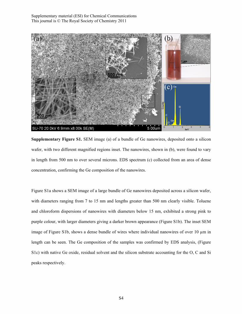
Supplementary Figure S1. SEM image (a) of a bundle of Ge nanowires, deposited onto a silicon
wafer, with two different magnified regions inset. The nanowires, shown in (b), were found to vary
in length from 500 nm to over several microns. EDS spectrum (c) collected from an area of dense
concentration, confirming the Ge composition of the nanowires.
Figure S1a shows a SEM image of a large bundle of Ge nanowires deposited across a silicon wafer,
with diameters ranging from 7 to 15 nm and lengths greater than 500 nm clearly visible. Toluene
and chloroform dispersions of nanowires with diameters below 15 nm, exhibited a strong pink to
purple colour, with larger diameters giving a darker brown appearance (Figure S1b). The inset SEM
image of Figure S1b, shows a dense bundle of wires where individual nanowires of over 10 µm in
length can be seen. The Ge composition of the samples was confirmed by EDS analysis, (Figure
S1c) with native Ge oxide, residual solvent and the silicon substrate accounting for the O, C and Si
peaks respectively.

Supplementary material (ESI) for Chemical Communications This journal is © The Royal Society of Chemistry 2011
S5
Supplementary Figure S2. XPS spectra obtained from samples of as synthesised Ge nanowires,
with higher resolution scans from both the Ge 3d and Ge 2p3/2 spectral regions highlighted in the
insets.
XPS was used to quantitatively examine the elemental composition and in particular the extent of
oxidation of the nanowires as, like Si, Ge is highly prone to surface oxidation. A low-resolution
survey scan of squalene synthesised nanowires drop cast onto oxidized silicon substrates, yielded
peak positions for Ge, O, C and Si. Peaks at binding energies 285 and 532 eV correspond to C 1s

Supplementary material (ESI) for Chemical Communications This journal is © The Royal Society of Chemistry 2011
S6
and O 1s, indicating the presence of residual organic solvent and probable surface oxidation of the
sample including oxygen from the substrate. With a detection limit of approximately 0.1 at%, XPS
analysis found no unintentional metal contamination that may have facilitated nanowire growth. For
Ge, high resolution spectra of both Ge 3d and 2p core level regions were recorded as shown in
Figure S2. The Ge 3d spectrum has two peaks belonging to Ge and a third peak assigned to O 2s.
The peak centered at a binding energy of 29.3 eV can be resolved into a doublet of narrow peaks
(Ge 3d5/2 and 3d3/2) and is in good agreement with expected values for elemental Ge. Oxidation of
Ge gives rise to chemical shifts ranging from 0.8 to 3.4 eV depending on the degree of oxidation.
The peaks at higher binding energies, 30.8 and 32 2 eV can therefore be associated with the native
oxides, GeO and GeO2 respectively. However, the Ge 2p photoelectrons which have low kinetic
energies and smaller escape depth compared to 3d photoelectrons are more sensitive to surface
properties and act as an excellent probe of the surface. The Ge 2p3/2 spectrum (Figure S2) is fitted
with a peak at 1217.1 eV which corresponds to elemental Ge15 and the two other component peaks
at higher binding energies correspond to GeOx. The relatively higher contribution of oxides (70%)
to Ge 2p compared to Ge 3d (40%) suggests that the oxides are localized on the surface of the
nanowires as expected.

Supplementary material (ESI) for Chemical Communications This journal is © The Royal Society of Chemistry 2011
S7
Supplementary Figure S3. Raman analysis from Ge samples showing the peak position for
squalane synthesised nanowires (a) to be slightly down-shifted compared to that of squalene based
samples (b).
Raman analysis, shown in Figure S3a and 3b, gives confirmation that both samples have a
predominant single composition of Ge, with peak positions at 298.1 and 300.3 cm-1 respectively.
The down-shifted position of the Ge peak for squalene can be related to a quantum confinement
effect seen for nanowires with diameters below their Bohr excitation radius. It is also noticeable that
each peak is asymmetric in shape, with a similar shoulder broadening out towards 265 cm-1 clearly
visible from both graphs. This shoulder can be attributed to the presence of Ge oxide in the sample,
where Raman scattering between 250 and 300 cm-1 is typical. The existence of native Ge oxide in
the samples was to be expected given that the samples of Ge nanowires where exposed to
atmospheric conditions during analysis.

Supplementary material (ESI) for Chemical Communications This journal is © The Royal Society of Chemistry 2011
S8
Nanowire Growth Mechanism
We believe that the NW growth mechanism in this report is similar to the mechanism proposed by
Zaitseva et al1 where an organic droplet acts as a sink for Ge vapour molecules allowing the
anisotropic growth of NWs in a tip growth model. Ge incorporation into these polymerized droplets
is followed by Ge crystallization at the solid-liquid interface in a complete analogue to the classic
VLS mechanism.
The use of a high boiling point solvent squalene and similar reaction temperatures support the
conditions required for this mechanistic pathway. Furthermore, the DPG used follows a well
understood thermal degradation pattern for NW growth.2 The importance of phenyl groups in
facilitating unseeded Ge NW production was first proposed by Heath et al.3 The use of a solid
nucleation surface in our study allows higher density NW formation than that possible in previous
solution based methods. This is due to the substrate acting as a site for organic droplet formation.
The <50 nm size of the NW diameters presented here is consistent with the previous organic seeded
report where with our tighter diameter distribution is likely due to the more precise temperature
control feasible within the three zone furnace used. The consistency of NW diameter across the
three substrates used in this study (i.e. Pyrex, quartz and ITO) is consistent with the formation of
organic droplets of a defined size as opposed to surface defect driven growth. The density of the
NWs formed on the flask was found to depend on the concentration of DPG injected into the
reaction, however, the nature of the NWs produced (i.e. average diameter and length) was found to
be independent of both reaction time and concentration. The absence of an increased yield with
respect to time can be linked to the Ge monomer source being exhausted within the reactor.
1. N. Zaitseva, J. Harper, D. Gerion and C. Saw, Applied Physics Letters, 2005, 86, 053105-
053105-053103. 2. G. Collins, M. Kolesnik, V. Krstic and J. D. Holmes, Chemistry of Materials, 2010, 22,
5235-5243. 3. J. R. Heath and F. K. Legoues, Chem. Phys. Lett., 1993, 208, 263-268.

Supplementary material (ESI) for Chemical Communications This journal is © The Royal Society of Chemistry 2011
S9